WO2019181558A1 - 光センサー回路、光センサー装置、および、表示装置 - Google Patents
光センサー回路、光センサー装置、および、表示装置 Download PDFInfo
- Publication number
- WO2019181558A1 WO2019181558A1 PCT/JP2019/009306 JP2019009306W WO2019181558A1 WO 2019181558 A1 WO2019181558 A1 WO 2019181558A1 JP 2019009306 W JP2019009306 W JP 2019009306W WO 2019181558 A1 WO2019181558 A1 WO 2019181558A1
- Authority
- WO
- WIPO (PCT)
- Prior art keywords
- switching transistor
- transistor
- gate
- light receiving
- period
- Prior art date
- Legal status (The legal status is an assumption and is not a legal conclusion. Google has not performed a legal analysis and makes no representation as to the accuracy of the status listed.)
- Ceased
Links
Images

Classifications
-
- H—ELECTRICITY
- H10—SEMICONDUCTOR DEVICES; ELECTRIC SOLID-STATE DEVICES NOT OTHERWISE PROVIDED FOR
- H10F—INORGANIC SEMICONDUCTOR DEVICES SENSITIVE TO INFRARED RADIATION, LIGHT, ELECTROMAGNETIC RADIATION OF SHORTER WAVELENGTH OR CORPUSCULAR RADIATION
- H10F30/00—Individual radiation-sensitive semiconductor devices in which radiation controls the flow of current through the devices, e.g. photodetectors
- H10F30/20—Individual radiation-sensitive semiconductor devices in which radiation controls the flow of current through the devices, e.g. photodetectors the devices having potential barriers, e.g. phototransistors
- H10F30/21—Individual radiation-sensitive semiconductor devices in which radiation controls the flow of current through the devices, e.g. photodetectors the devices having potential barriers, e.g. phototransistors the devices being sensitive to infrared, visible or ultraviolet radiation
- H10F30/28—Individual radiation-sensitive semiconductor devices in which radiation controls the flow of current through the devices, e.g. photodetectors the devices having potential barriers, e.g. phototransistors the devices being sensitive to infrared, visible or ultraviolet radiation the devices being characterised by field-effect operation, e.g. junction field-effect phototransistors
- H10F30/282—Insulated-gate field-effect transistors [IGFET], e.g. MISFET [metal-insulator-semiconductor field-effect transistor] phototransistors
-
- H—ELECTRICITY
- H10—SEMICONDUCTOR DEVICES; ELECTRIC SOLID-STATE DEVICES NOT OTHERWISE PROVIDED FOR
- H10F—INORGANIC SEMICONDUCTOR DEVICES SENSITIVE TO INFRARED RADIATION, LIGHT, ELECTROMAGNETIC RADIATION OF SHORTER WAVELENGTH OR CORPUSCULAR RADIATION
- H10F55/00—Radiation-sensitive semiconductor devices covered by groups H10F10/00, H10F19/00 or H10F30/00 being structurally associated with electric light sources and electrically or optically coupled thereto
- H10F55/18—Radiation-sensitive semiconductor devices covered by groups H10F10/00, H10F19/00 or H10F30/00 being structurally associated with electric light sources and electrically or optically coupled thereto wherein the radiation-sensitive semiconductor devices and the electric light source share a common body having dual-functionality of light emission and light detection
-
- G—PHYSICS
- G02—OPTICS
- G02F—OPTICAL DEVICES OR ARRANGEMENTS FOR THE CONTROL OF LIGHT BY MODIFICATION OF THE OPTICAL PROPERTIES OF THE MEDIA OF THE ELEMENTS INVOLVED THEREIN; NON-LINEAR OPTICS; FREQUENCY-CHANGING OF LIGHT; OPTICAL LOGIC ELEMENTS; OPTICAL ANALOGUE/DIGITAL CONVERTERS
- G02F1/00—Devices or arrangements for the control of the intensity, colour, phase, polarisation or direction of light arriving from an independent light source, e.g. switching, gating or modulating; Non-linear optics
- G02F1/01—Devices or arrangements for the control of the intensity, colour, phase, polarisation or direction of light arriving from an independent light source, e.g. switching, gating or modulating; Non-linear optics for the control of the intensity, phase, polarisation or colour
- G02F1/13—Devices or arrangements for the control of the intensity, colour, phase, polarisation or direction of light arriving from an independent light source, e.g. switching, gating or modulating; Non-linear optics for the control of the intensity, phase, polarisation or colour based on liquid crystals, e.g. single liquid crystal display cells
- G02F1/133—Constructional arrangements; Operation of liquid crystal cells; Circuit arrangements
- G02F1/1333—Constructional arrangements; Manufacturing methods
-
- G—PHYSICS
- G06—COMPUTING OR CALCULATING; COUNTING
- G06F—ELECTRIC DIGITAL DATA PROCESSING
- G06F1/00—Details not covered by groups G06F3/00 - G06F13/00 and G06F21/00
- G06F1/16—Constructional details or arrangements
- G06F1/1601—Constructional details related to the housing of computer displays, e.g. of CRT monitors, of flat displays
- G06F1/1605—Multimedia displays, e.g. with integrated or attached speakers, cameras, microphones
-
- G—PHYSICS
- G06—COMPUTING OR CALCULATING; COUNTING
- G06F—ELECTRIC DIGITAL DATA PROCESSING
- G06F3/00—Input arrangements for transferring data to be processed into a form capable of being handled by the computer; Output arrangements for transferring data from processing unit to output unit, e.g. interface arrangements
- G06F3/01—Input arrangements or combined input and output arrangements for interaction between user and computer
- G06F3/03—Arrangements for converting the position or the displacement of a member into a coded form
- G06F3/041—Digitisers, e.g. for touch screens or touch pads, characterised by the transducing means
- G06F3/042—Digitisers, e.g. for touch screens or touch pads, characterised by the transducing means by opto-electronic means
-
- G—PHYSICS
- G09—EDUCATION; CRYPTOGRAPHY; DISPLAY; ADVERTISING; SEALS
- G09F—DISPLAYING; ADVERTISING; SIGNS; LABELS OR NAME-PLATES; SEALS
- G09F9/00—Indicating arrangements for variable information in which the information is built-up on a support by selection or combination of individual elements
-
- H—ELECTRICITY
- H10—SEMICONDUCTOR DEVICES; ELECTRIC SOLID-STATE DEVICES NOT OTHERWISE PROVIDED FOR
- H10D—INORGANIC ELECTRIC SEMICONDUCTOR DEVICES
- H10D86/00—Integrated devices formed in or on insulating or conducting substrates, e.g. formed in silicon-on-insulator [SOI] substrates or on stainless steel or glass substrates
- H10D86/40—Integrated devices formed in or on insulating or conducting substrates, e.g. formed in silicon-on-insulator [SOI] substrates or on stainless steel or glass substrates characterised by multiple TFTs
- H10D86/421—Integrated devices formed in or on insulating or conducting substrates, e.g. formed in silicon-on-insulator [SOI] substrates or on stainless steel or glass substrates characterised by multiple TFTs having a particular composition, shape or crystalline structure of the active layer
- H10D86/423—Integrated devices formed in or on insulating or conducting substrates, e.g. formed in silicon-on-insulator [SOI] substrates or on stainless steel or glass substrates characterised by multiple TFTs having a particular composition, shape or crystalline structure of the active layer comprising semiconductor materials not belonging to the Group IV, e.g. InGaZnO
-
- H—ELECTRICITY
- H10—SEMICONDUCTOR DEVICES; ELECTRIC SOLID-STATE DEVICES NOT OTHERWISE PROVIDED FOR
- H10D—INORGANIC ELECTRIC SEMICONDUCTOR DEVICES
- H10D86/00—Integrated devices formed in or on insulating or conducting substrates, e.g. formed in silicon-on-insulator [SOI] substrates or on stainless steel or glass substrates
- H10D86/40—Integrated devices formed in or on insulating or conducting substrates, e.g. formed in silicon-on-insulator [SOI] substrates or on stainless steel or glass substrates characterised by multiple TFTs
- H10D86/60—Integrated devices formed in or on insulating or conducting substrates, e.g. formed in silicon-on-insulator [SOI] substrates or on stainless steel or glass substrates characterised by multiple TFTs wherein the TFTs are in active matrices
-
- H—ELECTRICITY
- H10—SEMICONDUCTOR DEVICES; ELECTRIC SOLID-STATE DEVICES NOT OTHERWISE PROVIDED FOR
- H10F—INORGANIC SEMICONDUCTOR DEVICES SENSITIVE TO INFRARED RADIATION, LIGHT, ELECTROMAGNETIC RADIATION OF SHORTER WAVELENGTH OR CORPUSCULAR RADIATION
- H10F30/00—Individual radiation-sensitive semiconductor devices in which radiation controls the flow of current through the devices, e.g. photodetectors
- H10F30/20—Individual radiation-sensitive semiconductor devices in which radiation controls the flow of current through the devices, e.g. photodetectors the devices having potential barriers, e.g. phototransistors
- H10F30/21—Individual radiation-sensitive semiconductor devices in which radiation controls the flow of current through the devices, e.g. photodetectors the devices having potential barriers, e.g. phototransistors the devices being sensitive to infrared, visible or ultraviolet radiation
- H10F30/289—Individual radiation-sensitive semiconductor devices in which radiation controls the flow of current through the devices, e.g. photodetectors the devices having potential barriers, e.g. phototransistors the devices being sensitive to infrared, visible or ultraviolet radiation the devices being transparent or semi-transparent devices
-
- H—ELECTRICITY
- H10—SEMICONDUCTOR DEVICES; ELECTRIC SOLID-STATE DEVICES NOT OTHERWISE PROVIDED FOR
- H10D—INORGANIC ELECTRIC SEMICONDUCTOR DEVICES
- H10D30/00—Field-effect transistors [FET]
- H10D30/60—Insulated-gate field-effect transistors [IGFET]
- H10D30/67—Thin-film transistors [TFT]
- H10D30/6729—Thin-film transistors [TFT] characterised by the electrodes
- H10D30/673—Thin-film transistors [TFT] characterised by the electrodes characterised by the shapes, relative sizes or dispositions of the gate electrodes
- H10D30/6733—Multi-gate TFTs
- H10D30/6734—Multi-gate TFTs having gate electrodes arranged on both top and bottom sides of the channel, e.g. dual-gate TFTs
Definitions
- the present invention relates to an optical sensor circuit, and is particularly applicable to an optical sensor circuit, an optical sensor device, and a display device using an oxide semiconductor transistor.
- Patent Document 1 JP 2011-243950 A (Patent Document 1) and JP 2009-182194 A (Patent Document 2) have been proposed as an optical sensing circuit or an optical sensor element using an oxide semiconductor transistor.
- An oxide semiconductor transistor has a deterioration mode called optical negative bias deterioration in which a threshold voltage greatly fluctuates when a negative bias is applied while irradiating light.
- optical negative bias deterioration in which a threshold voltage greatly fluctuates when a negative bias is applied while irradiating light.
- the oxide semiconductor transistor is irradiated with light, the drain current decreases very slowly even if the light irradiation is stopped. Therefore, there is a problem that it is difficult to use an oxide semiconductor transistor for an optical sensor element.
- An object of the present invention is to provide an optical sensor circuit using an oxide semiconductor transistor capable of performing a stable operation.
- the optical sensor circuit includes a light receiving transistor, a first switching transistor, a second switching transistor, and a capacitive element.
- the light receiving transistor includes a gate connected to the first wiring, a source connected to the second wiring, and a drain.
- the first switching transistor includes a gate connected to a third wiring, a source connected to a fourth wiring, and a drain connected to the drain of the light receiving transistor.
- the capacitive element includes a first terminal connected to the drain of the light receiving transistor and a second terminal connected to the source of the first switching transistor.
- the second switching transistor includes a gate connected to a gate line, a source connected to a signal line, and a drain connected to the first terminal of the capacitor.
- Each of the light receiving transistor, the first switching transistor, and the second switching transistor includes an oxide semiconductor layer as a channel layer.
- the photosensor device includes the plurality of gate lines, the plurality of signal lines, and the plurality of gate lines and the plurality of signal lines so that one photosensor circuit is connected to one gate line and one signal line.
- Each of the plurality of photosensor circuits includes a light receiving transistor, a first switching transistor, a second switching transistor, and a capacitive element.
- the light receiving transistor includes a gate connected to the first wiring, a source connected to the second wiring, and a drain.
- the first switching transistor includes a gate connected to a third wiring, a source connected to a fourth wiring, and a drain connected to the drain of the light receiving transistor.
- the capacitive element has a first terminal connected to the drain of the light receiving transistor and a second terminal connected to the source of the first switching transistor.
- the second switching transistor includes a gate connected to a corresponding gate line, a source connected to a corresponding signal line, and a drain connected to the first terminal of the capacitive element.
- Each of the light receiving transistor, the first switching transistor, and the second switching transistor includes an oxide semiconductor layer as a channel layer.
- the display device has a display panel having a display area.
- the display area includes display pixels and a photosensor circuit.
- the photosensor circuit includes a light receiving transistor, a first switching transistor, a second switching transistor, and a capacitive element.
- the light receiving transistor includes a gate connected to the first wiring, a source connected to the second wiring, and a drain.
- the first switching transistor includes a gate connected to a third wiring, a source connected to a fourth wiring, and a drain connected to the drain of the light receiving transistor.
- the capacitive element includes a first terminal connected to the drain of the light receiving transistor and a second terminal connected to the source of the first switching transistor.
- the second switching transistor includes a gate connected to a gate line, a source connected to a signal line, and a drain connected to the first terminal of the capacitor.
- Each of the light receiving transistor, the first switching transistor, and the second switching transistor includes an oxide semiconductor layer as a channel layer.
- FIG. 2 is a cross-sectional view schematically illustrating an exemplary structure of the light receiving transistor in FIG. 1.
- FIG. 2 is a cross-sectional view schematically illustrating an exemplary structure of the switching transistor of FIG. 1. It is a figure which shows the characteristic of the drain current of the light reception transistor when there is no light irradiation. It is a figure which shows the characteristic of the drain current of a light reception transistor in case there exists light irradiation.
- It is a circuit diagram explaining the example of an example structure of the optical sensor circuit which concerns on an Example. It is a block diagram which shows the example whole structure of the optical sensor apparatus which concerns on an Example.
- FIG. 12 is a diagram exemplarily showing a gate bias potential (Vg) of a gate electrode of an oxide semiconductor transistor when a reset pulse is applied in FIG. 12 is a diagram exemplarily showing a drain bias potential (Vd) of a drain electrode of an oxide semiconductor transistor when a reset pulse is applied in FIG. 11 is a plan view conceptually showing a display device according to application example 1.
- Vg gate bias potential
- Vd drain bias potential
- FIG. 12 is a plan view conceptually showing a display device according to application example 2.
- FIG. It is a top view which shows notionally the display apparatus which concerns on a modification.
- FIG. 1 is a cross-sectional view schematically illustrating an exemplary structure of an oxide semiconductor transistor used in the photosensor device according to the example.
- FIG. 2 is a cross-sectional view schematically illustrating an exemplary structure of the light receiving transistor 101 of FIG.
- FIG. 3 is a cross-sectional view schematically illustrating an exemplary structure of the switching transistor 102 of FIG.
- the optical sensor device 1 includes a plurality of optical sensor circuits SC.
- one light receiving transistor 101, one switching transistor 102, and capacitive element 103 that are used in each photosensor circuit SC are illustrated. Both the light receiving transistor 101 and the switching transistor 102 are configured using oxide semiconductor transistors.
- the light receiving transistor 101 includes a gate electrode 12b, an oxide semiconductor layer 14b, a drain electrode 15b, and a source electrode 15c. That is, the light receiving transistor 101 is a lower gate structure in which the gate electrode 12b is provided below the oxide semiconductor layer 14b, that is, a bottom gate type three-terminal (gate, source, and drain) element. It has a bottom gate / top contact structure (called an inverted stagger structure).
- the switching transistor 102 includes a gate electrode 12a, an oxide semiconductor 14a, a source electrode 15a and a drain electrode 15b, and a back gate electrode 17. That is, the switching transistor 102 is a bottom-gate type four-terminal (gate, source, drain, and back gate) element, and has a configuration in which the back gate electrode 17 is provided in an inverted staggered structure.
- the switching transistor 102 may be a dual gate drive that drives the gate electrode 12 a and the back gate electrode 17.
- the switching transistor 102 may have a configuration in which the back gate electrode 17 is connected to the source electrode 15a.
- the switching transistor 102 is not limited to the bottom gate type configuration, and may have a top gate type configuration.
- the upper gate structure is a structure in which the gate electrode 12a is provided above the oxide semiconductor 14a.
- the capacitive element 103 includes a gate electrode 12c, a source or drain electrode 15d, and a gate insulating film 13.
- the capacitor 103 is not limited to this structure, and can include the gate electrode 12c, the oxide semiconductor layer provided simultaneously with the oxide semiconductor layers 14a and 14b, and the gate insulating film 13. Further, the capacitor 103 can be constituted by the source or drain electrode 15 d, a metal layer provided simultaneously with the back gate electrode 17, and the insulating layer 16.
- the oxide semiconductor layers 14a and 14b constitute channel layers (active layers) of the oxide semiconductor transistors (101 and 102), and the material thereof can include an oxide semiconductor material such as a ZnO-based material.
- the ZnO-based material may include, for example, ZnO, or at least one material selected from Hf, Y, Ta, Zr, Ti, Cu, Ni, Cr, In, Ga, Al, Sn, and Mg Can also include a mixture or compound containing ZnO.
- such a ZnO-based material can include ZnO, TaZnO, InZnO (IZO), and GaInZnO (Gallium Indium Zinc Oxide; GIZO).
- Such an oxide semiconductor transistor can be used as the light receiving transistor 101 because the threshold voltage and the drain current change depending on the amount of incident light LIG.
- the switching transistor 102 does not need to change the threshold voltage and the drain current depending on the amount of incident light LIG. Therefore, as shown in FIGS. 1 and 3, a gate is provided below the oxide semiconductor layer 14a.
- An electrode 12a is provided, and a back gate electrode 17 is provided above the oxide semiconductor layer 14a.
- the oxide semiconductor layer 14a of the switching transistor 102 is configured not to be irradiated with the incident light LIG. That is, the back gate electrode 17 has a function of blocking or blocking incident light LIG to the oxide semiconductor layer 14a.
- the optical sensor device 1 includes a substrate 10, an insulating layer 11 provided entirely on the substrate 10, and gate electrodes 12 a, 12 b, 12 c partially provided on the insulating layer 11. And the insulating layer 11 and the gate insulating film 13 provided on the gate electrodes 12a, 12b, and 12c so as to cover the side surfaces and the upper surface of the gate electrodes 12a, 12b, and 12c.
- the optical sensor device 1 further includes oxide semiconductor layers 14a and 14b partially provided on the gate insulating film 13, and source and drain electrodes provided so as to cover both sides of the oxide semiconductor layers 14a and 14b.
- the optical sensor device 1 further includes a back gate electrode 17 partially provided on the transparent insulating layer 16 so as to cover the oxide semiconductor layer 14a, and the entire back gate electrode 17 and the transparent insulating layer 16.
- a transparent insulating layer 20 as a protective film provided so as to cover the whole.
- the wiring layer 19a is connected to the back gate electrode 17 via a via electrode
- the wiring layer 19b is connected to the source electrode 15c via a via electrode.
- the substrate 10 can use a general substrate material such as glass, silicon, or a resin substrate.
- the insulating layer 11, the gate insulating film 13, the transparent insulating layer 16, the transparent insulating layer 18, and the transparent insulating layer 20 can be made of a silicon oxide film material.
- the insulating layer 11, the gate insulating film 13, the transparent insulating layer 16, the transparent insulating layer 18, and the transparent insulating layer 20 can be formed by a CVD method.
- the gate electrodes 12a, 12b, 12c, the source and drain electrodes 15a, 15b, 15c, 15d, the back gate electrode 17, and the wiring layers 19a, 19b can use a conductive metal or a conductive metal oxide.
- the oxide semiconductor layers 14a and 14b can be formed by a sputtering method.
- the gate electrodes 12a, 12b, and 12c, and the source and drain electrodes 15a, 15b, 15c, and 15d are transparent such as ITO. It can be made of a conductive material.
- the back gate electrode 17 irradiates the oxide semiconductor layer 14a with the incident light LIG.
- the back gate electrode 17 is preferably made of an opaque conductive material because it has a role of shielding or blocking light.
- the gate electrode 12c blocks or blocks the irradiation of the incident light LIG to the oxide semiconductor layer 14a. Since it has a blocking function, the gate electrode 12c is preferably made of an opaque conductive material.
- FIG. 4 is a diagram showing the drain current characteristics of the light receiving transistor 101 when there is no light irradiation.
- FIG. 5 is a diagram showing the drain current characteristics of the light receiving transistor 101 when there is light irradiation. 4 and FIG. 5, the vertical axis indicates the drain current value of the light receiving transistor 101, and the horizontal axis indicates the gate voltage of the light receiving transistor 101. The characteristic indicated by the dotted line indicates the case where the drain voltage is 1V, and the characteristic indicated by the solid line indicates the case where the drain voltage is 10V.
- the drain current is The value is very small, such as below the lower limit of measurement.
- the drain current increases significantly as compared with FIG.
- the value of the drain current of the light receiving transistor 101 in an off state (herein also referred to as an off current) is set as shown in FIGS. It can be used to determine the presence or absence of light irradiation.
- an off current the value of the drain current of the light receiving transistor 101 in an off state
- the signal ratio of the off-current of the light receiving transistor 101 in the presence or absence of light irradiation is large, it is possible to detect the presence or absence of light irradiation in a stable operation.
- the oxide semiconductor transistor has a deterioration mode called optical negative bias deterioration in which the threshold voltage greatly fluctuates when a negative bias is applied while irradiating light.
- optical negative bias deterioration in which the threshold voltage greatly fluctuates when a negative bias is applied while irradiating light.
- the trade-off that the photodegradation is accelerated when the photosensitivity is increased is a problem.
- the light-receiving transistor 101 since the off-state current of an oxide semiconductor transistor is very low, the light-receiving transistor 101 has a three-terminal structure, and the light-receiving transistor 101 is operated in an off region, so that a sufficient signal ratio of off-state current with and without light irradiation is obtained be able to.
- the light irradiation amount between the two elements 101 and 102 can be controlled. Thereby, it is possible to detect the presence or absence of light irradiation with a stable operation.
- the photodegradation of the oxide semiconductor transistor moves the threshold value in the negative direction. Therefore, when the oxide semiconductor transistor is turned off, the negative potential applied to the gate electrode is increased, thereby affecting the negative fluctuation of the threshold value. It is possible to make it difficult to receive.
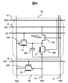
- FIG. 6 is a circuit diagram illustrating an exemplary configuration example of the optical sensor circuit according to the embodiment.
- the optical sensor circuit SC includes a light receiving transistor 101 that is a light receiving element, a switching transistor 102, a switching transistor 104, and a capacitive element 103.
- a reset circuit RS connected to the photosensor circuit SC is depicted.
- the reset circuit RS includes a switching transistor 105.
- each of the switching transistors 104 and 105 is formed of an oxide semiconductor transistor having a back gate electrode 17, similarly to the switching transistor 102 described with reference to FIGS. 1 and 3.
- each of the switching transistors 102, 104, and 105 has a configuration in which the back gate electrode 17 is connected to the source electrode.
- the switching transistor 102 may be referred to as a first switching transistor, the switching transistor 104 as a second switching transistor, and the switching transistor 105 as a third switching transistor.
- the light receiving transistor 101 is connected to the gate connected to the wiring (first wiring) L1 to which the first gate control signal SVG is supplied and the wiring (second wiring) L2 to the wiring to which the first source control signal SVS is supplied.
- the switching transistor 102 is connected to a gate connected to the wiring (third wiring) L3 to which the second gate control signal DCH is supplied and to a wiring (fourth wiring) L4 to which the second source control signal VR1 is supplied.
- Capacitance element 103 has a first terminal connected to the drain of light-receiving transistor 101 and a second terminal connected to the source of switching transistor 102.
- the switching transistor 104 has a gate connected to the gate line G1, a source connected to the signal line Sig1, and a drain connected to the first terminal of the capacitor 103.
- the capacitor element 103 has a function of storing charges according to the amount of light irradiated when the light receiving transistor 101 is irradiated with the incident light LIG.
- the charge stored in the capacitor 103 is read out to the signal line Sig1 through the source / drain path of the switching transistor 104 which is turned on when the gate line G1 is set to the selection level.
- the reset circuit RS has a switching transistor 105.
- the switching transistor 105 is connected to the gate connected to the wiring (fifth wiring) L5 to which the reset signal RST is supplied, the source connected to the wiring L4 to which the second source control signal VR1 is supplied, and the signal line Sig1. Drain.
- the wiring L4 to which the second source control signal VR1 is supplied is connected to the second terminal of the capacitor 103 of each photosensor circuit SC when a plurality of photosensor circuits SC are provided.
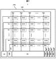
- FIG. 7 is a block diagram illustrating an exemplary overall configuration of the optical sensor device according to the embodiment.
- FIG. 7 shows a plurality of wirings other than the light receiving transistor 101, the switching transistors 102 and 104, the capacitor 103, the gate line G, and the signal line S shown in FIG. L1-L4) are not described.
- the photosensor device 1 is provided on, for example, a rectangular photosensor panel LPNL.
- An array unit ARR is provided on the photosensor panel LPNL, and the array unit ARR includes a plurality of photosensor circuits (SC11, SC12,...) Arranged in a matrix such as m rows and n columns, for example. , SCmn).
- m gate lines G (G1, G2, G3,..., Gm) are provided, and n signal lines S (Sig1, Sig2, Sig3,. ., Sign).
- Photosensor circuits SC11, SC12, SC13,. . . , SC1n is connected to the gate line G1
- the optical sensor circuits SC21, SC22, SC23,. . . , SC2n is connected to the gate line G2
- the optical sensor circuits SC31, SC32, SC33,. . . , SC3n is connected to a gate line G3.
- a plurality of photosensor circuits arranged in corresponding rows are connected to the other gate lines.
- the optical sensor circuits SC11, SC21, SC31,. . . , SCm1 is connected to the signal line Sig1
- the optical sensor circuits SC12, SC22, SC32,. . . , SCm2 is connected to the signal line Sig2
- the optical sensor circuits SC13, SC23, SC33,. . . , SCm3 is connected to a signal line Sig3.
- a plurality of photosensor circuits arranged in corresponding columns are connected to the other signal lines.
- the plurality of photosensor circuits are connected to the plurality of gate lines and the plurality of signal lines so that one photosensor circuit is connected to one gate line and one signal line. Is done.
- a reset circuit RS1, RS2, RS3,. . . RSn there are a plurality of reset circuits RS1, RS2, RS3,. . . RSn), a reset control circuit RSTL, a gate line driving circuit GD, and a reading circuit RA.
- a plurality of reset circuits (RS1, RS2, RS3,..., RSn) are provided corresponding to each column.
- the reset circuit RS1 is connected to the signal line Sig1
- the reset circuit RS2 is connected to the signal line Sig2
- the reset circuit RS3 is connected to the signal line Sig3.
- other reset circuits are connected to corresponding signal lines.
- a reset signal RST output from the reset control circuit RSTL is also input to the plurality of reset circuits (RS1, RS2, RS3,..., RSn) via a wiring.
- the gate line driving circuit GD is connected to m gate lines G (G1, G2, G3,..., Gm), for example, m gate lines G (G1, G2, G3,..., Gm). ) Has a function of setting a desired one gate line to a selection level.
- Read circuit RA is connected to n signal lines S (Sig1, Sig2, Sig3, ..., Sign). For example, in the read operation, when the gate line driving circuit GD sets one gate line to the selection level, a plurality of photosensor circuits connected to the gate line set to the selection level are selected. Then, the charges stored in the capacitive elements in the selected plurality of photosensor circuits are input as read data to the read circuit RA via the n signal lines.
- the read circuit RA can have an analog-digital conversion circuit function for converting an analog signal into a digital signal, for example. Thereby, an analog signal such as the amount of electric charge read from the capacitive element of the photosensor circuit can be converted into a digital signal and transmitted to, for example, a host device.
- a control circuit SVGL that generates the first gate control signal SVG and a control circuit SVSL that generates the first source control signal SVS are also provided in the area around the area where the array unit ARR is provided.
- a control circuit DCHL for generating the second gate control signal DCH and a control circuit VR1L for generating the second source control signal VR1 are provided.
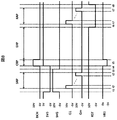
- FIG. 8 is a timing diagram illustrating an operation example of the optical sensor device 1 according to the embodiment.
- the timing diagram of FIG. 8 shows one sensor sequence.
- One sensor sequence includes a sensor reset period SRP, a capacity reset period CRP, an exposure period EXP, and a readout period RAP.
- Such a sensor sequence is performed, for example, continuously or a predetermined number of times in a desired period to perform touch detection or fingerprint detection.
- the sensor reset period SRP is a period in which the optical response of the light receiving transistor 101 is canceled by returning a reset current to the light receiving transistor 101 by the switching transistor 105 and is returned to the initial state.
- the photocurrent is instantaneously reset by making the bias of the gate electrode of the light receiving transistor 101 positive.
- the capacitance reset period CRP is a period in which the charge stored in the capacitor 103 is changed to a constant potential by the switching transistor 102 before the exposure period EXP.
- the exposure period EXP is a period in which the light receiving transistor 101 functions as a light receiving element and charges are stored in the capacitor 103 according to the amount of light irradiated by the incident light LIG. In the exposure period EXP, sufficient signal strength is ensured by making the bias of the gate electrode of the light receiving transistor 101 negative.
- the readout period RAP is a period in which a signal proportional to the amount of light irradiated by the incident light LIG is read from the charge newly stored in the capacitive element 103 by turning on the switching transistor 104 after the exposure period EXP. is there.
- the light intensity of the light irradiation of the incident light LIG on the light receiving transistor 101 can be quantitatively detected.
- the period t1 indicates a preparation period that is performed before the sensor reset period SRP.
- the first gate control signal SVG is set to a high level such as 10V
- the reset signal RST is set to a high level such as 10V.
- the second gate control signal DCH is set to a low level such as -5V
- the first source control signal SVS is set to a low level such as -1V
- the second source control signal VR1 is set to a high level such as 0V.
- All the gate electrodes G1-Gm are set to a low level (non-selection level) such as ⁇ 5V. In this state, the light receiving transistor 101 and the switching transistor 105 are on.
- the sensor reset period SRP After the period t1, the sensor reset period SRP is started.
- the sensor reset period SRP has a plurality of periods t2.
- a period t2 indicates a period in which each of the gate electrodes (G1-Gm) is sequentially shifted from a non-selection level such as ⁇ 5V to a selection level such as 10V and then transitions to a non-selection level. .
- the gate electrode G1 is set to the selection level, the optical response of the light receiving transistor 101 in each photosensor circuit (SC11, SC12,..., SC1n) in the first row connected to the gate electrode G1 is canceled, Returns to the initial state.
- the gate electrode G2 When the gate electrode G2 is set to the selection level, the optical response of the light receiving transistor 101 in each photosensor circuit (SC21, SC22,..., SC2n) in the second row connected to the gate electrode G2 is canceled, Returns to the initial state.
- a similar operation sequentially sets the other gate electrodes (G3-Gm) to the selection level, whereby the light receiving transistors 101 in all the optical sensor circuits of the sensor array ARR are returned to the initial state. Specifically, the switching transistor 105, the switching transistor 104, and the light receiving transistor 101 are turned on.
- the reset current is supplied from the wiring to which the second source control signal VR1 is supplied to the source / drain path of the switching transistor 105, the signal line (Sig1-Sign), the source / drain path of the switching transistor 104, and the light receiving transistor 101. Flows through the source / drain path to the wiring to which the first source control signal SVS is supplied.
- the period t3 indicates the period when the selection operation of all the gate electrodes (G3-Gm) is completed.
- the period t4 is provided after the period t3 and indicates a preparation period that is performed before the capacity reset period CRP.
- the first gate control signal SVG is changed from a high level such as 10V to a low level such as ⁇ 5V.
- the period t5 indicates a capacity reset period CRP provided after the period t4.
- the second gate control signal DCH is changed from a low level such as -5V to a high level such as 10V
- the second source control signal VR1 is changed from a high level such as 0V to a low level such as -1V.
- the first source control signal SVS is changed from a low level such as ⁇ 1V to a high level such as 5V.
- the switching transistor 102 is turned on, and the electric charge stored in the capacitor 103 is discharged or charged to change to a constant potential. To do.
- the exposure period EXP is provided after the period t5.
- the second gate control signal DCH is changed from a high level such as 10V to a low level such as -5V
- the second source control signal VR1 is changed from a low level such as -1V to a high level such as 0V.
- the light receiving transistor 101, the switching transistor 102, and the switching transistor 104 in all the optical sensor circuits are in an off state.
- each light receiving transistor 101 in the photosensor circuit (SC11, SC12,..., SCnm) functions as a light receiving element and is irradiated with the incident light LIG. Electric charge is stored in each capacitor 103 according to the amount of light.
- the end of the exposure period EXP is determined by transitioning the reset signal RST from a high level such as 10V to a low level such as ⁇ 5V. That is, the exposure period EXP can be determined by the time between the transition of the second gate control signal DCH to the low level and the transition of the reset signal RST to the low level. Therefore, the exposure period EXP can be varied by controlling this time.
- the period t6 is a preparation period before the reading period RAP.
- the reset signal RST is set to a low level.
- Read period RAP is started after period t6.
- the read period RAP has a plurality of periods t7.
- a period t7 indicates a period in which each of the gate electrodes (G1-Gm) is sequentially shifted from a non-selection level such as ⁇ 5V to a selection level such as 10V, and then transitions to a non-selection level. .
- the gate electrode G1 is set to the selection level, the charge newly stored in each capacitor 103 in each photosensor circuit (SC11, SC12,..., SC1n) connected to the gate electrode G1 in the first row.
- the switching transistor 104 is turned on, the signal is read out to the signal lines Sig1-Sign and input to the readout circuit RA.
- the readout circuit RA By sequentially setting all the gate electrodes (G2-Gm) to the selection level, the charges of all the capacitive elements 103 of all the optical sensor circuits (SC11, SC12,..., SCmn) in the array part ARR are read out by the readout circuit RA. Is input.
- the period t8 is provided after the end of the reading period RAP. After the period t8, the reset signal RST transitions from the low level to the high level, so that the state of each signal is set to the state before the start of the period t1.
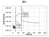
- FIG. 9 is a characteristic diagram for explaining the characteristics of the photocurrent of the oxide semiconductor transistor according to the comparative example.
- the vertical axis indicates the drain current
- the horizontal axis indicates time (seconds: S).
- FIG. 9 shows changes in drain current (photocurrent) when a simple two-terminal or oxide semiconductor transistor to which no reset bias is applied is irradiated with light for 10 to 30 seconds on the horizontal axis. .
- light irradiation ON when light irradiation ON), the drain current of the oxide semiconductor transistor increases.
- light irradiation is stopped (non-light irradiation OFF)
- the drain current of the oxide semiconductor transistor is increased.
- the drain current decreases very slowly. Note that the drain current (photocurrent) increased by the light irradiation does not easily decrease even after the light irradiation is stopped, and has a characteristic that it remains higher than the original current value before the light irradiation for one hour or longer.
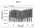
- FIG. 10 is a diagram for explaining the photocurrent of the oxide semiconductor transistor according to the comparative example.
- the vertical axis represents the drain current
- the horizontal axis represents time (second: S).
- the voltage applied to the LED element employed as the light emitting element is shown on the upper side of FIG. That is, FIG. 10 shows the drain current (photocurrent) of an oxide semiconductor transistor when a simple two-terminal or oxide semiconductor transistor to which no reset bias is applied is irradiated with light while changing the light emission amount of the LED element. Changes are shown.
- a simple two-terminal or oxide semiconductor transistor to which no reset bias is applied has a very slow light relaxation, so that a stable signal intensity cannot be obtained, and a quantitative optical sensor. It can be seen that it is difficult to form an element using an oxide semiconductor transistor.
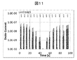
- FIG. 11 is a diagram for explaining the photocurrent of the oxide semiconductor transistor according to the example.
- the vertical axis represents the drain current
- the horizontal axis represents time (seconds: S).
- the voltage applied to the LED element is shown as in FIG. 10. 11 illustrates a case where a three-terminal oxide semiconductor transistor 101 is used as an oxide semiconductor transistor, and a positive voltage is applied as a reset pulse to the gate terminal G1 of the oxide semiconductor transistor 101 at the start of sensing or at the end of sensing. A change in drain current (photocurrent) of the oxide semiconductor transistor 101 is shown. As understood from FIG.
- the refresh period can be significantly reduced to, for example, 100 msec or less. Therefore, a stable signal intensity can be obtained, and it becomes possible to form a quantitative photosensor element with an oxide semiconductor transistor.
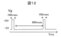
- FIG. 12 is a diagram exemplarily showing the gate bias potential (Vg) of the gate electrode of the oxide semiconductor transistor 101 when the reset pulse of FIG. 11 is applied.
- Vg gate bias potential
- a positive potential which is set to a high level (10 V) can be applied to the gate electrode of the oxide semiconductor transistor 101 as a reset pulse, for example, for a period of 100 msec.
- the interval between the reset pulses is illustratively 900 msec.
- the high-level period of the reset pulse in FIG. 12 can be regarded as one period t2 in the sensor reset period SRP shown in FIG.
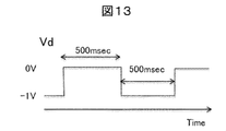
- FIG. 13 is a diagram exemplarily showing the drain bias potential (Vd) of the drain electrode of the oxide semiconductor transistor 101 when the reset pulse of FIG. 11 is applied.
- the drain electrode of the oxide semiconductor transistor 101 is set to a high level (0 V) for a period such as 500 msec, and is then set to a low level ( ⁇ 1 V) for a period such as 500 msec.
- the period in which the bias potential (Vd) in FIG. 13 is at the low level ( ⁇ 1V) can be regarded as the capacitance reset period CRP (period t5) shown in FIG.
- the light receiving transistor 101 is an oxide semiconductor element having three terminals (gate, source, and drain) using the oxide semiconductor layer 14b as a channel layer (active layer). Since the light receiving transistor 101 has a three-terminal structure, as shown in FIGS. 4 and 5, it is possible to use the value of the drain current (off current) in the off state of the light receiving transistor 101 to determine the presence or absence of light irradiation. I can do it. By utilizing the fact that the signal ratio of the off-state current of the light receiving transistor 101 in the presence or absence of light irradiation is large, it is possible to detect the presence or absence of light irradiation in a stable operation.
- the switching transistor 102 (104, 105) is an oxide semiconductor element having four terminals (gate, source, drain, and back gate) using the oxide semiconductor layer 14a as a channel layer (active layer).
- the oxide semiconductor layer 14a of the switching transistor 102 is configured not to be irradiated with the incident light LIG.
- the back gate electrode 17 has a function of blocking or blocking incident light LIG to the oxide semiconductor layer 14a.
- the switching transistor 102 (104, 105) may be a dual gate drive for driving the gate electrode 12a and the back gate electrode 17.
- the switching transistor 102 (104, 105) may have a configuration in which the back gate electrode 17 is connected to the source electrode 15a.
- the switching transistor 102 (104, 105) is not limited to the bottom gate type structure, and may have a top gate type structure.
- the optical sensor circuit includes a light receiving transistor 101, switching transistors 102 and 104, and a capacitive element 103.
- the light receiving transistor 101 has a gate connected to a wiring to which the first gate control signal SVG is supplied, a source connected to a wiring to which the first source control signal SVS is supplied, and a drain.
- the switching transistor 102 is connected to the gate connected to the wiring to which the second gate control signal DCH is supplied, the source connected to the wiring to which the second source control signal VR1 is supplied, and the drain of the light receiving transistor 101. And a drain.
- Capacitance element 103 has a first terminal connected to the drain of light-receiving transistor 101 and a second terminal connected to the source of switching transistor 102.
- the switching transistor 104 has a gate connected to the gate line G1, a source connected to the signal line Sig1, and a drain connected to the first terminal of the capacitor 103.
- the charge stored in the capacitor 103 is read out to the signal line Sig1 through the source / drain path of the switching transistor 104 which is turned on when the gate line G1 is set to the selection level.
- the reset circuit RS is connected to the photosensor circuit.
- the reset circuit RS includes a switching transistor 105.
- the switching transistor 105 has a gate connected to the wiring to which the reset signal RST is supplied, a source connected to the wiring to which the second source control signal VR1 is supplied, and a drain connected to the signal line Sig1. .
- one sensor sequence includes a sensor reset period SRP, a capacitance reset period CRP, an exposure period EXP, and a readout period RAP.
- the sensor reset period SRP is a period in which the optical response of the light receiving transistor 101 is canceled by returning a reset current to the light receiving transistor 101 by the switching transistor 105 and is returned to the initial state.
- the capacitance reset period CRP is a period in which the charge stored in the capacitor 103 is changed (initialized) to a constant potential by the switching transistor 102 before the exposure period EXP.
- the exposure period EXP is a period in which the light receiving transistor 101 functions as a light receiving element, and charges are stored in the capacitive element 103 according to the amount of light irradiated by the incident light LIG.
- the readout period RAP is a period in which a signal proportional to the amount of light irradiated by the incident light LIG is read from the charge newly stored in the capacitive element 103 by turning on the switching transistor 104 after the exposure period EXP. is there.
- the optical sensor device 1 capable of performing stable operation can be provided.
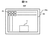
- FIG. 14 is a plan view conceptually showing the display device according to the application example 1.
- FIG. The display device DSP according to the application example 1 illustrates a configuration example when the optical sensor device 1 according to the embodiment is used as a fingerprint sensor.
- the optical sensor device 1 is attached to a desired region on the display panel PNL of the display device DSP.
- This area is, for example, the area of the display panel PNL assigned to the fingerprint detection area.
- the display panel PNL has a display area DA, and the display area DA has a plurality of display pixels PX arranged in a matrix.
- the display panel PNL can be a liquid crystal display panel, for example. In this case, a liquid crystal display pixel can be used for each of the plurality of display pixels PX.
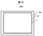
- FIG. 15 is a plan view conceptually showing a display device according to application example 2.
- FIG. The display device DSP1 according to the application example 2 illustrates a configuration example in the case where the optical sensor device 1 of the embodiment is used as a touch sensor.
- the optical sensor device 1 is attached to the display area DA of the display panel PNL of the display device DSP.
- the display panel PNL includes a display area DA
- the display area DA includes a plurality of display pixels PX arranged in a matrix.
- the optical sensor device 1 of the application example 2 is not limited to a touch sensor, and can also be used as a fingerprint sensor.
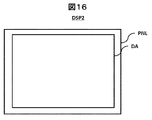
- FIG. 16 is a plan view conceptually showing a display device according to a modification. 14 and 15 show a configuration example in which the optical sensor device 1 of the embodiment is bonded to the display area DA of the display panel PNL.
- the display device DSP2 according to the modification both the display pixel PX and the photosensor circuit SC are provided in the display area DA of the display panel PNL.
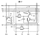
- FIG. 17 is a circuit diagram showing a configuration example of the display pixel PX and the photosensor circuit SC that can be employed in the display device according to the modification.
- FIG. 17 exemplarily shows a configuration in which the photosensor circuit SC of FIG. 6 and the display pixel PX are combined.
- the configuration of the photosensor circuit SC is the same as that shown in FIG.
- the display pixel PX includes one thin film transistor TFT as a switching element.
- the thin film transistor TFT has a gate connected to a pixel gate line PXG1 that is a scanning line, one source / drain connected to a pixel source line S1 that is a signal line, and the other source / drain connected to a pixel electrode PE.
- the display pixel PX is provided with a common electrode Vcom that applies a common potential Vcom to all the display pixels PX, and a liquid crystal layer LC is provided between the pixel electrode PE and the common electrode Vcom.
- the thin film transistor TFT is turned on / off based on a drive signal supplied via the pixel gate line PXG1, and a pixel voltage is applied to the pixel electrode PE based on a display signal supplied from the pixel source line S1 when the thin film transistor TFT is on.
- the liquid crystal layer LC is driven by the electric field between the pixel electrode PE and the common electrode Vcom.
- FIG. 17 shows a configuration in which one photosensor circuit SC is provided for one display pixel PX, but is not limited thereto.
- One photosensor circuit SC may be provided for a plurality of display pixels PX.
- one photosensor circuit SC may be provided for five display pixels PX.
- a liquid crystal display device is disclosed as an example of a display device.
- the liquid crystal display device can be used for various devices such as a smartphone, a tablet terminal, a mobile phone terminal, a personal computer, a television receiver, an in-vehicle device, a game machine, a digital camera, and a video camera.
- main structures disclosed in the application examples and the modification examples include a self-luminous display device (OLED) having an organic electroluminescence display element and the like, an electronic paper display device having an electrophoretic element and the like, MEMS (Micro
- OLED self-luminous display device
- MEMS Micro
- the present invention can also be applied to a display device applying Electro (Mechanical Systems) or a display device applying electrochromism.
- the light-receiving transistor 101 using an oxide semiconductor layer has a very low off-current, and therefore can keep a very low off-current without light irradiation. Therefore, the exposure time (exposure period EXP) and readout time (readout period RAP) can be freely changed according to the purpose and irradiation light (global shutter). For example, when an OLED or liquid crystal display device is combined, the optical sensor device 1 can be driven or the optical sensor device 1 can be operated independently between display operations of the OLED or liquid crystal display device. . In the case where the reading time (reading period RAP) is shortened, a polycrystalline low-temperature polysilicon (LTPS) thin film transistor (TFT) can be used for the reading transistor 104 and the reset transistor 105.
- LTPS polycrystalline low-temperature polysilicon
- TFT thin film transistor
- Various inventions can be formed by appropriately combining a plurality of constituent elements disclosed in the above embodiment. For example, some components may be deleted from all the components shown in the embodiment. Furthermore, you may combine suitably the component covering different embodiment.
Landscapes
- Engineering & Computer Science (AREA)
- Physics & Mathematics (AREA)
- Theoretical Computer Science (AREA)
- General Engineering & Computer Science (AREA)
- General Physics & Mathematics (AREA)
- Human Computer Interaction (AREA)
- Nonlinear Science (AREA)
- Multimedia (AREA)
- Computer Hardware Design (AREA)
- Chemical & Material Sciences (AREA)
- Mathematical Physics (AREA)
- Crystallography & Structural Chemistry (AREA)
- Optics & Photonics (AREA)
- Solid State Image Pick-Up Elements (AREA)
- Composite Materials (AREA)
- Thin Film Transistor (AREA)
- Light Receiving Elements (AREA)
- Devices For Indicating Variable Information By Combining Individual Elements (AREA)
- Liquid Crystal (AREA)
Priority Applications (5)
| Application Number | Priority Date | Filing Date | Title |
|---|---|---|---|
| CN201980020363.2A CN111868940B (zh) | 2018-03-20 | 2019-03-08 | 光传感器电路、光传感器装置及显示装置 |
| US17/024,725 US11189745B2 (en) | 2018-03-20 | 2020-09-18 | Light sensor circuit, light sensor device, and display device |
| US17/527,192 US11575062B2 (en) | 2018-03-20 | 2021-11-16 | Light sensor circuit, light sensor device, and display device |
| US18/091,388 US11973161B2 (en) | 2018-03-20 | 2022-12-30 | Photo sensor device |
| US18/597,953 US20240213393A1 (en) | 2018-03-20 | 2024-03-07 | Photo sensor device |
Applications Claiming Priority (2)
| Application Number | Priority Date | Filing Date | Title |
|---|---|---|---|
| JP2018052337A JP7039346B2 (ja) | 2018-03-20 | 2018-03-20 | 光センサー回路、光センサー装置、および、表示装置 |
| JP2018-052337 | 2018-03-20 |
Related Child Applications (1)
| Application Number | Title | Priority Date | Filing Date |
|---|---|---|---|
| US17/024,725 Continuation US11189745B2 (en) | 2018-03-20 | 2020-09-18 | Light sensor circuit, light sensor device, and display device |
Publications (1)
| Publication Number | Publication Date |
|---|---|
| WO2019181558A1 true WO2019181558A1 (ja) | 2019-09-26 |
Family
ID=67987072
Family Applications (1)
| Application Number | Title | Priority Date | Filing Date |
|---|---|---|---|
| PCT/JP2019/009306 Ceased WO2019181558A1 (ja) | 2018-03-20 | 2019-03-08 | 光センサー回路、光センサー装置、および、表示装置 |
Country Status (4)
| Country | Link |
|---|---|
| US (4) | US11189745B2 (https=) |
| JP (1) | JP7039346B2 (https=) |
| CN (1) | CN111868940B (https=) |
| WO (1) | WO2019181558A1 (https=) |
Cited By (3)
| Publication number | Priority date | Publication date | Assignee | Title |
|---|---|---|---|---|
| CN111508986A (zh) * | 2020-04-29 | 2020-08-07 | Tcl华星光电技术有限公司 | 一种传感器及其制作方法以及光电转换装置 |
| CN111508987A (zh) * | 2020-04-29 | 2020-08-07 | Tcl华星光电技术有限公司 | 一种传感器及其制作方法以及光电转换装置 |
| JP2023177282A (ja) * | 2022-05-31 | 2023-12-13 | エルジー ディスプレイ カンパニー リミテッド | 薄膜トランジスタ、及びこれを含む表示装置 |
Families Citing this family (6)
| Publication number | Priority date | Publication date | Assignee | Title |
|---|---|---|---|---|
| JP7039346B2 (ja) * | 2018-03-20 | 2022-03-22 | 株式会社ジャパンディスプレイ | 光センサー回路、光センサー装置、および、表示装置 |
| JP7576474B2 (ja) | 2021-01-26 | 2024-10-31 | 株式会社ジャパンディスプレイ | 検出装置 |
| KR102820522B1 (ko) * | 2021-04-30 | 2025-06-17 | 삼성디스플레이 주식회사 | 표시 장치 및 그 제조 방법 |
| US12295194B2 (en) | 2021-04-30 | 2025-05-06 | Samsung Display Co., Ltd. | Display device including protective layer overlapping backplane line and method of manufacturing the same |
| CN113451422B (zh) * | 2021-06-30 | 2023-06-06 | 中国科学技术大学 | 一种光电探测器的调节方法及其应用 |
| JPWO2024176379A1 (https=) * | 2023-02-22 | 2024-08-29 |
Citations (5)
| Publication number | Priority date | Publication date | Assignee | Title |
|---|---|---|---|---|
| US20120138919A1 (en) * | 2010-12-03 | 2012-06-07 | E Ink Holdings Inc. | Photo sensing unit and photo sensor thereof |
| JP2012256819A (ja) * | 2010-09-08 | 2012-12-27 | Semiconductor Energy Lab Co Ltd | 半導体装置 |
| WO2015111118A1 (ja) * | 2014-01-27 | 2015-07-30 | 株式会社Joled | 有機el表示装置および駆動方法 |
| JP2015216369A (ja) * | 2014-04-23 | 2015-12-03 | 株式会社半導体エネルギー研究所 | 撮像装置 |
| US20160291714A1 (en) * | 2015-03-30 | 2016-10-06 | Boe Technology Group Co., Ltd. | Touch Panel, Method For Fabricating the Same and Touch Display Device |
Family Cites Families (8)
| Publication number | Priority date | Publication date | Assignee | Title |
|---|---|---|---|---|
| KR101003170B1 (ko) * | 2006-09-25 | 2010-12-22 | 인테그레이티드 디지털 테크놀로지스, 인코포레이티드 | 광 검출기 어레이 |
| JP5121478B2 (ja) | 2008-01-31 | 2013-01-16 | 株式会社ジャパンディスプレイウェスト | 光センサー素子、撮像装置、電子機器、およびメモリー素子 |
| US8569807B2 (en) * | 2009-09-01 | 2013-10-29 | Taiwan Semiconductor Manufacturing Company, Ltd. | Backside illuminated image sensor having capacitor on pixel region |
| KR101672344B1 (ko) | 2010-05-20 | 2016-11-04 | 삼성전자주식회사 | 광센싱 회로, 상기 광센싱 회로의 구동 방법, 및 상기 광센싱 회로를 채용한 광센싱 장치 |
| US8716646B2 (en) * | 2010-10-08 | 2014-05-06 | Semiconductor Energy Laboratory Co., Ltd. | Photoelectric conversion device and method for operating the same |
| JP5529203B2 (ja) * | 2011-09-21 | 2014-06-25 | シャープ株式会社 | 光センサおよび電子機器 |
| JP6725335B2 (ja) * | 2016-06-20 | 2020-07-15 | 株式会社ジャパンディスプレイ | 半導体装置 |
| JP7039346B2 (ja) * | 2018-03-20 | 2022-03-22 | 株式会社ジャパンディスプレイ | 光センサー回路、光センサー装置、および、表示装置 |
-
2018
- 2018-03-20 JP JP2018052337A patent/JP7039346B2/ja active Active
-
2019
- 2019-03-08 CN CN201980020363.2A patent/CN111868940B/zh active Active
- 2019-03-08 WO PCT/JP2019/009306 patent/WO2019181558A1/ja not_active Ceased
-
2020
- 2020-09-18 US US17/024,725 patent/US11189745B2/en active Active
-
2021
- 2021-11-16 US US17/527,192 patent/US11575062B2/en active Active
-
2022
- 2022-12-30 US US18/091,388 patent/US11973161B2/en active Active
-
2024
- 2024-03-07 US US18/597,953 patent/US20240213393A1/en active Pending
Patent Citations (5)
| Publication number | Priority date | Publication date | Assignee | Title |
|---|---|---|---|---|
| JP2012256819A (ja) * | 2010-09-08 | 2012-12-27 | Semiconductor Energy Lab Co Ltd | 半導体装置 |
| US20120138919A1 (en) * | 2010-12-03 | 2012-06-07 | E Ink Holdings Inc. | Photo sensing unit and photo sensor thereof |
| WO2015111118A1 (ja) * | 2014-01-27 | 2015-07-30 | 株式会社Joled | 有機el表示装置および駆動方法 |
| JP2015216369A (ja) * | 2014-04-23 | 2015-12-03 | 株式会社半導体エネルギー研究所 | 撮像装置 |
| US20160291714A1 (en) * | 2015-03-30 | 2016-10-06 | Boe Technology Group Co., Ltd. | Touch Panel, Method For Fabricating the Same and Touch Display Device |
Cited By (5)
| Publication number | Priority date | Publication date | Assignee | Title |
|---|---|---|---|---|
| CN111508986A (zh) * | 2020-04-29 | 2020-08-07 | Tcl华星光电技术有限公司 | 一种传感器及其制作方法以及光电转换装置 |
| CN111508987A (zh) * | 2020-04-29 | 2020-08-07 | Tcl华星光电技术有限公司 | 一种传感器及其制作方法以及光电转换装置 |
| US11804508B2 (en) | 2020-04-29 | 2023-10-31 | Tcl China Star Optoelectronics Technology Co., Ltd. | Sensor, manufacturing method thereof, and photoelectric conversion device |
| JP2023177282A (ja) * | 2022-05-31 | 2023-12-13 | エルジー ディスプレイ カンパニー リミテッド | 薄膜トランジスタ、及びこれを含む表示装置 |
| JP7646733B2 (ja) | 2022-05-31 | 2025-03-17 | エルジー ディスプレイ カンパニー リミテッド | 薄膜トランジスタ、及びこれを含む表示装置 |
Also Published As
| Publication number | Publication date |
|---|---|
| JP7039346B2 (ja) | 2022-03-22 |
| JP2019165130A (ja) | 2019-09-26 |
| US20210005771A1 (en) | 2021-01-07 |
| US20240213393A1 (en) | 2024-06-27 |
| US20230137257A1 (en) | 2023-05-04 |
| CN111868940B (zh) | 2023-12-08 |
| US11189745B2 (en) | 2021-11-30 |
| US20220077344A1 (en) | 2022-03-10 |
| US11575062B2 (en) | 2023-02-07 |
| CN111868940A (zh) | 2020-10-30 |
| US11973161B2 (en) | 2024-04-30 |
Similar Documents
| Publication | Publication Date | Title |
|---|---|---|
| JP7039346B2 (ja) | 光センサー回路、光センサー装置、および、表示装置 | |
| CN209471965U (zh) | 光传感器装置以及显示装置 | |
| CN111435587B (zh) | 具有混合像素内和外部补偿的电子显示器 | |
| US9268428B2 (en) | Light-sensing apparatuses, methods of driving the light-sensing apparatuses, and optical touch screen apparatuses including the light-sensing apparatuses | |
| US8896577B2 (en) | Optical touch screen apparatuses and methods of driving the optical touch screen apparatuses | |
| CN100454538C (zh) | 晶体管阵列及其制造方法、以及图像处理器件 | |
| TW594770B (en) | Shift register and electronic apparatus | |
| US9035910B2 (en) | Touch sensing and remote sensing optical touch screen apparatuses | |
| KR20210013488A (ko) | 표시장치 및 표시장치의 구동 방법 | |
| WO2017054408A1 (zh) | 像素驱动电路、显示面板及其驱动方法和显示装置 | |
| CN104167177A (zh) | 像素电路、有机电致发光显示面板及显示装置 | |
| JP6180712B2 (ja) | 単純化された光センシング回路、前記光センシング回路を含む光センシング装置、前記光センシング装置を駆動する方法、及び前記光センシング装置を含む画像取得装置及び光タッチスクリーン装置 | |
| JP2023552225A (ja) | 低減された温度輝度感度を有するディスプレイ | |
| JP4645047B2 (ja) | シフトレジスタ回路及びその駆動制御方法並びに駆動制御装置 | |
| JP5275739B2 (ja) | センサ素子およびその駆動方法 | |
| JP7736919B2 (ja) | カソードノイズを軽減するためのディスプレイを有する電子デバイス | |
| JP7667297B2 (ja) | 低減された温度輝度感度を有するディスプレイ | |
| JP7326518B2 (ja) | 光センサー装置 | |
| JP2014116608A (ja) | 半導体装置及び表示装置 | |
| KR20170117965A (ko) | 광터치 스크린 장치 및 그 구동 방법 | |
| JP2025077259A (ja) | 表示装置 | |
| KR101951322B1 (ko) | 광센싱 장치 및 그 구동 방법, 광센싱 장치를 포함하는 광터치 스크린 장치 | |
| KR102514895B1 (ko) | 표시 장치 | |
| JP5448258B2 (ja) | フォトセンサ | |
| JP2007035098A (ja) | シフトレジスタ、撮像装置、表示装置 |
Legal Events
| Date | Code | Title | Description |
|---|---|---|---|
| 121 | Ep: the epo has been informed by wipo that ep was designated in this application |
Ref document number: 19772505 Country of ref document: EP Kind code of ref document: A1 |
|
| NENP | Non-entry into the national phase |
Ref country code: DE |
|
| 122 | Ep: pct application non-entry in european phase |
Ref document number: 19772505 Country of ref document: EP Kind code of ref document: A1 |