WO2019181544A1 - フォワードフライバック方式の絶縁型スイッチング電源 - Google Patents
フォワードフライバック方式の絶縁型スイッチング電源 Download PDFInfo
- Publication number
- WO2019181544A1 WO2019181544A1 PCT/JP2019/009159 JP2019009159W WO2019181544A1 WO 2019181544 A1 WO2019181544 A1 WO 2019181544A1 JP 2019009159 W JP2019009159 W JP 2019009159W WO 2019181544 A1 WO2019181544 A1 WO 2019181544A1
- Authority
- WO
- WIPO (PCT)
- Prior art keywords
- current
- reactor
- switching element
- bypass
- current path
- Prior art date
- Legal status (The legal status is an assumption and is not a legal conclusion. Google has not performed a legal analysis and makes no representation as to the accuracy of the status listed.)
- Ceased
Links
Images










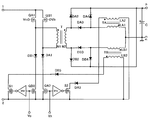
Classifications
-
- H—ELECTRICITY
- H02—GENERATION; CONVERSION OR DISTRIBUTION OF ELECTRIC POWER
- H02M—APPARATUS FOR CONVERSION BETWEEN AC AND AC, BETWEEN AC AND DC, OR BETWEEN DC AND DC, AND FOR USE WITH MAINS OR SIMILAR POWER SUPPLY SYSTEMS; CONVERSION OF DC OR AC INPUT POWER INTO SURGE OUTPUT POWER; CONTROL OR REGULATION THEREOF
- H02M3/00—Conversion of DC power input into DC power output
- H02M3/22—Conversion of DC power input into DC power output with intermediate conversion into AC
- H02M3/24—Conversion of DC power input into DC power output with intermediate conversion into AC by static converters
- H02M3/28—Conversion of DC power input into DC power output with intermediate conversion into AC by static converters using discharge tubes with control electrode or semiconductor devices with control electrode to produce the intermediate AC
Definitions
- the present invention relates to an insulation type switching power supply, and more particularly to a forward flyback insulation type switching power supply.
- a switching power source that converts AC power to DC power
- a two-converter type isolated switching power source including a non-insulated boost converter as a power factor correction circuit and an isolated DC / DC converter at a subsequent stage
- a forward method and a flyback method As a typical method of the latter-stage insulated DC / DC converter, there are a forward method and a flyback method. The forward method is suitable for large output power supplies.
- a one-converter type isolated AC / DC converter having a power factor improving function is also known.
- the one-converter type isolated switching power supply is configured by a flyback method that operates substantially the same as a non-insulated boost converter.
- the flyback method has a power factor correction function, but is not suitable for a large output power source.
- the number of switching elements on the primary side of the insulated switching power supply may be one.
- a plurality of switching elements are disclosed as in Patent Document 3 and the like.
- a full bridge circuit, a push-pull circuit, and the like are known.
- the conventional one-converter type isolated switching power supply described above has several problems.
- the flyback method is usually adopted for the one-converter type isolated switching power supply.
- a withstand voltage characteristic is required for the switching element on the primary side. With a switching configuration such as a full bridge system, the withstand voltage characteristic is reduced, but there are cases where it cannot be adequately handled.
- a switching configuration such as a full bridge system
- two groups of switching elements that are turned on and off at an appropriate interval are provided, and MOSFETs are generally used as the switching elements.
- the body diode of the other group of FETs becomes forward biased against the back electromotive force generated in the primary coil of the transformer when one group of FETs is turned from on to off. Flowing. Such a recirculation reduces the power conversion efficiency of the switching power supply.
- the output current flows only when the electromotive force generated in the secondary coil of the transformer when the switching element is on exceeds the voltage of the smoothing capacitor at the output end. Therefore, no current is output in a range where the electromotive force of the secondary coil is small, which deteriorates the power factor.
- the present invention aims to reduce the breakdown voltage characteristics of the switching element while incorporating the advantages of both the flyback method and the forward method in an isolated switching power supply.
- the present invention provides the following configurations.
- -An aspect of the present invention is a transformer having a primary coil and a secondary coil; Switching having at least one switching element of the first group and at least one switching element of the second group, which are turned on and off in a mutually contradictory manner with a predetermined interval to conduct or cut off the current of the primary coil.
- a backflow prevention element connected in series to a current path including the primary coil in order to prevent the return to the input side due to the back electromotive force generated in the primary coil;
- a rectifier connected to the secondary coil;
- a smoothing unit including at least one reactor and a smoothing capacitor connected to a subsequent stage of the rectifying unit;
- the bypass current path is formed by temporarily shorting the reactor in a current path including the reactor, or the bypass current path includes a current path including the reactor. It is preferable that it is another current path through which the flyback current can flow without going through.
- the at least one reactor is a first and a second reactor; (A) a first external transformer comprising a primary coil that is the first reactor and a secondary coil; (B) a first short-circuit current path including the secondary coil of the first external transformer; (C) a first bypass switching element that is on / off controlled to turn on or off the first short-circuit current path; (D) a second external transformer comprising a primary coil as the second reactor and a secondary coil; (D) a second short-circuit current path including the secondary coil of the second external transformer; (E) a second bypass switching element that is on-off controlled to conduct or block the second short-circuit current path;
- the current path including the first or second reactor becomes the bypass current path when the first or second reactor is short-circuited.
- the bypass current path is another current path that allows the flyback current to flow without passing through the current path including the reactor
- D a second bypass switching element that is on / off controlled to conduct or block the second bypass current path
- the first or second bypass switching element is controlled so that the first or second bypass current path is conductive at least when a flyback current starts to flow through the secondary coil of the transformer.
- a first control voltage for controlling on / off of the first group of switching elements is input, and the second bypass switching element is turned on after a predetermined time from the time when the first control voltage is turned off.
- a second control voltage for ON / OFF control of the second group of switching elements is input, and the first bypass switching element is turned from ON to OFF after a predetermined time from the OFF point of the second control voltage. It is preferable to have a second timer IC that outputs a control voltage.
- the first capacitor connected to be applied as a control voltage of the first bypass switching element, the first capacitor being a voltage across the first capacitor;
- a second capacitor the second capacitor connected to be applied as a control voltage of the second bypass switching element, the second capacitor,
- the first capacitor is charged by a part of the forward current flowing through the secondary coil, and the current of the primary coil is cut off.
- the voltage across the first capacitor is equal to or higher than a certain voltage, the first bypass switching element is turned on.
- the second capacitor is charged by a part of the forward current flowing through the secondary coil, and the current of the primary coil is cut off.
- the second bypass switching element is turned on when the voltage across the second capacitor is equal to or higher than a certain voltage.
- the backflow prevention element is on a current path through which the current during the ON period of the first group of switching elements exclusively flows and on a current path through which the current during the ON period of the second group of switching elements exclusively flows.
- Each is preferably connected.
- the switching unit is configured based on any of a full bridge circuit, a push-pull circuit, or a half bridge circuit.
- the isolated switching power supply using the forward method and the flyback method according to the present invention has advantages of a large output by the forward method and a power factor improvement by the flyback method, and can suppress a spike at the time of flyback. It is possible to reduce the withstand voltage characteristics.
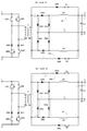
- FIG. 1 is a diagram schematically showing a circuit example of a first embodiment of an insulated switching power supply according to the present invention.
- FIG. 2 is a timing chart showing the control voltage of each switching element in the circuit of FIG.
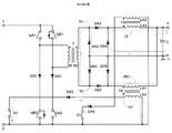
- FIG. 3 schematically shows the current that flows during the on period (mode-I) of the switching elements of group A in the circuit of FIG.
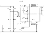
- FIG. 4 schematically shows a current flowing in the off period (mode-II) of the switching elements of group A in the circuit of FIG.
- FIG. 5 schematically shows the current that flows during the ON period (mode-III) of the switching elements of group B in the circuit of FIG.
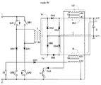
- FIG. 6 schematically shows the current flowing in the off period (mode-IV) of the switching elements of group B in the circuit of FIG.
- mode-IV off period
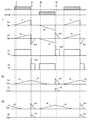
- FIG. 7 is a timing chart schematically showing examples of waveforms of voltages and currents in the circuit of FIG.
- FIG. 8 is a diagram schematically showing a circuit example of the second embodiment of the isolated switching power supply according to the present invention.
- FIG. 9A shows the current flowing in the off period (mode-II) of the switching elements in group A in the circuit of FIG. 8, and
- FIG. 9B shows the current flowing in the off period (mode-IV) of the switching elements in group B.
- the current is schematically shown.
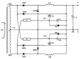
- FIG. 10 is a diagram schematically showing a circuit example of the third embodiment of the isolated switching power supply according to the present invention.
- FIG. 11A shows the current flowing in the off period (mode-II) of the switching element of group A in the circuit of FIG. 10, and FIG.
- FIG. 11B shows the off period (mode-IV) of the switching element in group B.
- the current is schematically shown.
- FIG. 12 is a timing chart showing an example of the control voltage of the bypass switching element in the circuits of the second and third embodiments.
- FIG. 13 is a timing chart showing another example of the control voltage of the bypass switching element in the circuits of the second and third embodiments.
- FIG. 14 shows an example of a control circuit that generates a control voltage for the bypass switching element.
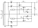
- FIG. 15 is a diagram schematically showing a circuit example of the fourth embodiment of the isolated switching power supply according to the present invention.
- FIG. 16 is an example of a timing diagram in the circuit of the fourth embodiment.
- FIG. 17A schematically shows the current flowing during the on period (mode-I) of the switching elements of group A in the circuit of FIG. 15, and FIG. 17B schematically shows the current flowing during the off period (mode-II).
- 18A schematically shows the current flowing in the on period (mode-III) of the switching elements of group B in the circuit of FIG. 15, and FIG. 18B schematically shows the current flowing in the off period (mode-IV).
- FIG. 19 is a diagram schematically showing a circuit example of the fifth embodiment of the isolated switching power supply according to the present invention.
- 20A schematically shows the current flowing during the on period (mode-I) of the switching elements of group A in the circuit of FIG. 19, and
- FIG. 20B schematically shows the current flowing during the off period (mode-II).
- FIG. 21A schematically shows the current flowing during the ON period (mode-III) of the switching elements of group B in the circuit of FIG. 19, and FIG. 21B schematically shows the current flowing during the OFF period (mode-IV).
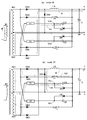
- FIGS. 22A and 22B are diagrams schematically showing another circuit example on the primary side of the transformer of the switching power supply according to the present invention.
- FIG. 23 is a diagram schematically illustrating a circuit example of a modification of the first embodiment.
- the insulated switching power supply of the present invention typically targets a one-converter AC / DC converter. Therefore, a typical input voltage in the switching power supply of the present invention is a rectified sine wave AC voltage. However, the switching power supply of the present invention can function similarly when the input voltage is a square wave or triangular wave voltage other than a sine wave or a constant voltage.
- FIG. 1 is a diagram schematically showing a circuit example of the first embodiment of the insulated switching power supply according to the present invention. .
- an input voltage obtained by full-wave rectification of an AC voltage is input to input terminals 1 and 2.
- the AC voltage here is, for example, a sine wave having a frequency of about several Hz to several tens Hz generated by a system power supply or various power generators.
- the waveform of the input voltage is not limited to a sine wave, and can be an arbitrary waveform having a positive potential.
- the transformer T which is the main transformer, is a forward transformer in which the primary coil N1 and the secondary coil N2 are wound with the same polarity (the winding start end of the coil is indicated by a black circle).
- a switching unit having a plurality of switching elements each of which is controlled to be turned on and off in order to conduct or cut off the current flowing through the primary coil N1 by the input voltage.
- the switching unit in FIG. 1 basically constitutes a full bridge circuit.
- This full bridge circuit includes four switching elements QA1, QA2, QB1, and QB2, and is an N-channel MOSFET as an example here.
- the full bridge circuit is suitable for a high-power switching power supply.
- the switching elements QA1 and QA2 constitute a first group (hereinafter referred to as “group A”) that is simultaneously turned on / off, and the switching elements QB1 and QB2 are simultaneously controlled to be turned on / off (hereinafter referred to as “group B”). ").
- Each switching element of the switching unit is on / off controlled by a control voltage applied to a gate which is a control terminal.
- the on / off control voltage in the switching unit on the primary side is a PWM signal.
- the frequency of the PWM signal is several tens kHz to several hundreds kHz higher than the frequency of the input AC.
- Each switching element of group A is ON / OFF controlled by control voltage V A
- each switching element of group B is ON / OFF controlled by control voltage V B.
- a switching element QA1 is connected in series between the positive input terminal 1 and the starting end of the primary coil N1. Between the terminal end of the primary coil N1 and the negative input terminal 2, a backflow prevention diode DA1 and a switching element QA2 are connected in series.
- a switching element QB1 is connected in series between the positive input terminal 1 and the end of the primary coil N1. Between the starting end of the primary coil N1 and the negative input terminal 2, a backflow prevention diode DB1 and a switching element QB2 are connected in series.
- backflow prevention diodes DA1 and DB1 are connected in series to a current path including a primary coil.
- the polarities of the backflow prevention diodes DA1 and DB1 are opposite to those of the body diodes of the switching elements QA1, QA2, QB1, and QB2.
- the backflow prevention diodes DA1 and DB1 can be inserted in series at any position on the current path between the input terminal 1 and the input terminal 2 other than the positions shown in FIG.
- the backflow prevention diodes DA1 and DB1 are inserted in current paths between the connection point between the drains of the switching element QA1 and the switching element QB1 and the connection point between the sources of the switching element QA2 and the switching element B2, respectively.
- the backflow prevention diode DA1 is inserted in series in the current path through which the on-period current of the switching elements of group A exclusively flows
- the backflow prevention diode DB1 is the current through which the on-period current of the switching elements of group B flows exclusively. It is preferred to be inserted in series in the path.
- the backflow prevention function can also be realized when a diode is inserted on at least one line of the input terminals 1 and 2.
- inserting a backflow prevention diode on the input line is disadvantageous in that a recovery current is generated when the switching element is turned off.
- a fast recovery diode (FRD), a Schottky diode using silicon carbide (SIC), or the like is used, a backflow prevention diode can be inserted on these input lines.
- bypass switching elements S1 and S2 are provided as other switching elements. These can also be MOSFETs as an example.
- the first bypass switching element S1 forms a first short-circuit current path together with the diode DA5 and the reactor LA2.
- Reactor LA2 is a secondary coil of a first external transformer TA provided on the secondary side described later.
- the diode DA5 has an anode connected to the start end of the reactor LA2 and a cathode connected to the drain of the switching element S1.
- the source of the switching element S1 and the end of the reactor LA2 are connected to the negative input terminal 2.
- the switching element S1 is on / off controlled to conduct or block the first short-circuit current path.
- the second bypass switching element S2 forms a second short-circuit current path together with the diode DB5 and the reactor LB2.
- Reactor LB2 is a secondary coil of a second external transformer TB provided on the secondary side described later.
- the diode DB5 has an anode connected to the start end of the reactor LB2, and a cathode connected to the drain of the switching element S2.
- the source of the switching element S2 and the end of the reactor LB2 are connected to the negative input terminal 2.
- the switching element S2 is on / off controlled to conduct or block the second short-circuit current path.
- the current flowing through the primary coils of the first and second external transformers TA and TB can take various values depending on the design of the switching power supply. In this case, by appropriately setting the turns ratio of the primary coils LA1 and LB1 and the secondary coils LA2 and LB2 according to the current flowing through the primary coil, even if the current flowing through the primary coil varies greatly, switching for bypassing is possible. Elements of the same standard can be used as the elements S1 and S2.
- the control voltage of the bypass switching element S1 is a voltage obtained by inverting the control voltage V A of the switching elements of the group A
- the control voltage of the bypass switching element S2 is control of the switching elements of the group B a voltage obtained by inverting the voltage V B.
- each of the bypass switching elements S1 and S2 can be controlled by a control voltage independent of the control voltage of each switching element of the full bridge circuit.
- a controller for generating and outputting a predetermined PWM signal as an on / off control voltage for each switching element shown in FIG. 1 is separately provided.
- the positive diode DA2 and negative diode DA3 that are the first pair are connected in series, and the positive diode DB2 and negative diode DB3 that are the second pair are connected in series.
- connection point of the first pair of diodes DA2 and DA3 connected in series is connected to the starting end of the secondary coil N2.
- the connection point of the second pair of diodes DB2 and DB3 connected in series is connected to the end of the secondary coil N2.
- the anodes of the negative diodes DA3 and DB3 are connected to the negative terminal of the smoothing capacitor C and the negative output terminal n.
- the cathodes of the positive diodes DA2 and DB2 are not connected to each other.
- the cathode of the positive diode DA2 is connected to the start end of the first reactor LA1, which is the primary coil of the first external transformer TA.
- the cathode of the positive diode DB2 is connected to the start end of the second reactor LB1, which is the primary coil of the second external transformer TB.
- Respective ends of the reactors LA1 and LB1 are connected to the positive terminal of the smoothing capacitor C and the positive output terminal p.
- Reactors LA1 and LB1 correspond to external series reactors in a forward type switching power supply.
- diodes DA4 and DB4 are provided as freewheeling diodes in a forward power supply.
- the anode of the diode DA4 is connected to the negative output terminal n, and the cathode is connected to the start point of the reactor LA1.
- the anode of the diode DB4 is connected to the negative output terminal n, and the cathode is connected to the starting point of the reactor LB1.
- the diodes DA4 and DB4 are not essential. When there is no diode DA4, diodes DA2 and DA3 can function as freewheeling diodes, and when there is no diode DB4, diodes DB2 and DB3 can function as freewheeling diodes.
- Reactors LA2 and LB2 that are secondary coils of the external transformers TA and TB are elements included in the circuit on the primary side of the transformer T as described above. With this configuration, it is possible to control the current flowing through the reactors LA1 and LB1 while ensuring insulation by using a control signal on the primary side of the transformer T.
- FIG. 2 is a timing chart showing an on / off control signal of each switching element in the circuit of FIG.
- FIG. 2A shows the control voltage V A of the switching elements of group A of the full bridge circuit.
- FIG. 2B shows the control voltage V B of the switching elements of group B of the full bridge circuit.
- FIG. 2C shows the control voltage V S1 of the bypass switching element S1 that conducts or cuts off the short-circuit current path including the reactor LA2.
- FIG. 2D shows the control voltage V S2 of the bypass switching element S2 that conducts or cuts off the short-circuit current path including the reactor LB2.
- the switching elements of group A and the switching elements of group B included in the full bridge circuit are provided with a predetermined interval (a period in which both groups are off). It is on / off controlled in contradiction. Both groups have the same length of the on period, and the length of the off period is the same.
- the control voltages of the bypass switching elements S1 and S2 are inverted voltages of the control voltages of the switching elements of the groups A and B, respectively.
- Mode I ON period of switching elements of group A
- Mode II OFF period of switching elements of group A
- Mode III ON period of switching elements of group B
- Mode IV OFF period of switching elements of group B
- FIG. 2 show an example of the time when a characteristic current flows in each of the four modes I, II, III, and IV.
- 3 to 6 schematically show characteristic currents flowing in the circuit of FIG. 1 at each of the four time points shown in FIG.
- FIG. 7 is a timing chart schematically showing examples of waveforms of voltages and currents in the circuit of FIG. 7A and 7B are the same control voltages V A and V B as those in FIGS. 2A and 2B, respectively.
- FIG. 7C shows the current I N1 flowing through the primary coil N1 of the transformer T
- FIG. 7D shows the current I N2 flowing through the secondary coil N2.
- 7E and 7F show the potential Vx at the start end and the potential Vy at the end of the secondary coil N2 of the transformer T, respectively.
- FIG. 7G shows the current I LA1 flowing through the primary coil LA1 of the transformer TA, and (h) shows the current I LA2 flowing through the secondary coil LA2.
- FIG. 7I shows the current I LB1 flowing through the primary coil LB1 of the transformer TB
- (j) shows the current I LB2 flowing through the secondary coil LB2. The operation in each mode will be described below with reference to FIGS.
- Mode I is the ON period of switching elements QA1 and QA2 of group A.
- a solid line with an arrow in FIG. 3 (mode-I) indicates a current immediately after the switching element of group A is turned on.
- a current i1 flows through the primary coil N1 (see FIG. 7C). This current i1 flows in the forward direction of the backflow prevention diode DA1.
- the reactor LA2 which is the secondary coil of the transformer TA, generates electromotive force when the current i2 flows through the reactor LA1, which is the primary coil. However, no current flows because the bypass switching element S1 is off.
- the smoothing capacitor C in the steady state is charged with a substantially constant voltage except for ripple fluctuation. Accordingly, the forward current i2 flows only when the electromotive force of the secondary coil N2 exceeds the voltage of the smoothing capacitor C. For example, when a sine wave input voltage is applied to the input terminals 1 and 2, the forward current i2 is not output to the output terminals p and n because the electromotive force of the secondary coil N2 is small in the range where the input voltage is small. This is a feature of the forward operation and causes a reduction in the power factor.
- Mode II is an off period of group A switching elements QA1 and QA2.
- the solid line and the dotted line with arrows in FIG. 4 (mode-II) indicate currents immediately after the switching elements of group A are turned off, respectively.
- the back electromotive force of the primary coil N1 is forward biased with respect to the body diodes of the switching elements QB1 and QB2 (see FIG. 4) of the group B.
- the backflow prevention diode DB1 is inserted in the current path, Reflux to is prevented. As a result, the energy returned to the input side when there is reflux remains in the transformer T in this circuit.
- the secondary coil N2 has a low potential at the start and a high potential at the end due to the counter electromotive force (see FIG. 7F).
- a current i3 that is a commutation current flows through the reactor LA1 via a freewheeling diode DA4 that is forward biased, and is output to the output terminal p and supplied to the load (FIG. 7 ( g)).
- the magnetic energy accumulated in the reactor LA1 during the ON period is released.
- the back electromotive force of the secondary coil N2 causes the diodes DA3 and DB2 to be forward-biased, and the flyback current ifb1 flows as shown by the dotted line with an arrow and passes through the reactor LB1 to output terminal p. And supplied to the load (see FIGS. 7D and 7I).
- the flyback current ifb1 is due to the release of magnetic energy retained in the transformer T because the reflux is blocked by the reverse-side prevention diode DB1 on the primary side.
- the flyback current ifb1 flows in the secondary coil N2, whereby the transformer T is magnetically reset.
- the flyback current ifb1 is output to the output terminal p with a magnitude corresponding to the magnitude of the back electromotive force even when the back electromotive force generated in the secondary coil N2 is small.
- the power factor is improved by the flyback current ifb1 flowing even in a range where the input voltage is small.
- the circuit of the present invention can be said to be a forward flyback method using both the forward method and the flyback method.
- Reactor LB1 is short-circuited, which is equivalent to a circuit in which flyback current ifb1 is output directly from the cathode of diode DB2 to positive output terminal p.
- reactor LB1 in mode II means that reactor LB1 has lost its reactor characteristics and is substantially equivalent to a conductor.
- the current path is hereinafter referred to as a “bypass current path for the flyback current. ".
- the bypass current path in the first embodiment is not a permanent circuit element, but is realized by temporarily shorting the reactor in a current path including the reactor.
- the bypass current path is realized by a permanent circuit element.
- the bypass current path is realized by another current path other than the current path including the reactor. Therefore, the flyback current bypass current path in the present invention may be realized by temporarily shorting the reactor or may be realized as a permanent circuit element.
- the condition for short-circuiting reactor LB1 when mode II flyback current ifb1 flows is that the short-circuit current path including reactor LB2 is at least when flyback current ifb1 starts to flow through reactor LB1. It is conducting.
- the bypass switching element S2 is maintained in the on state for a predetermined period including before and after the time point when the switching element of the group A is turned off from on, and the short-circuit current path is made conductive.
- the predetermined period may be a length necessary and sufficient for suppressing the spike voltage sp.
- FIG. 2 (d) it shows an example of the period to maintain the bypass switching element S2 to the ON state by the symbol t II.
- bypass switching element S2 is said to be in the off state even in the on state. Even if the bypass switching element S2 is in the ON state when the short-circuit current should not flow, the diode DB5 is reverse biased to prevent the short-circuit current.
- the ON period of the bypass switching element S2 is not overlapped with the ON period of the group B switching elements (in the circuit of FIG. 1, these control voltages are mutually inverted voltages so that they do not overlap each other). This is because the reactor LB1 in which the forward current i5 flows in the mode III, which will be described later, is short-circuited when the ON state of the group B switching element and the bypass switching element S2 overlap.
- Mode III is an ON period of switching elements QB1 and QB2 of group B. Mode III is substantially the same as mode I described above except that the current flows through a symmetrical path, and will be described briefly.
- the solid line with an arrow in FIG. 5 shows the current immediately after the group B switching elements are turned on.
- a current i4 flows through the primary coil N1 (see FIG. 7C).
- This current i1 flows in the forward direction of the backflow prevention diode DB1.
- the forward current i5 flows through the forward-biased diodes DA3 and DB2 (see FIG. 7 (d)) and is output through the reactor LB1. It is output to the terminal p and supplied to the load (see FIG. 7 (i)). Reactor LB1 is excited to accumulate magnetic energy.
- Mode IV is an off period of group B switching elements QB1 and QB2. Since mode IV is substantially the same as mode II described above except that the current flows through a symmetrical path, it will be briefly described.
- the solid line and the dotted line with arrows in FIG. 6 indicate currents immediately after the switching elements of group B are turned off, respectively.
- the group B switching elements are turned off, back electromotive force is generated in the primary coil N1 and the secondary coil N2.
- the back electromotive force of the primary coil N1 is forward biased with respect to the body diodes of the switching elements QA1 and QA2 of group A (see FIG. 6), but the backflow prevention diode DA1 is inserted in the current path, so that the input side Reflux to is blocked and energy remains in the transformer T.
- the secondary coil N2 has a high potential at the start and a low potential at the end due to the counter electromotive force (see FIG. 7E).
- a current i6 that is a commutation current flows through the reactor LB1 via a freewheeling diode DB4 that is forward biased, and is output to the output terminal p and supplied to the load (FIG. 7 ( i)).
- the magnetic energy accumulated in the reactor LB1 during the ON period is released.
- the diodes DB3 and DA2 are forward biased by the back electromotive force of the secondary coil N2 (see FIG. 7E).
- a flyback current ifb2 flows and is output to the output terminal p through the reactor LA1 and supplied to the load (see FIGS. 7D and 7G).
- the flyback current ifb2 is due to the release of magnetic energy retained in the transformer T because the reflux is blocked by the primary side backflow prevention diode DA1.
- Reactor LA1 is short-circuited, which is equivalent to a circuit in which flyback current ifb2 is directly output from the cathode of diode DA2 to positive output terminal p. Similar to the bypass current path of reactor LB1 in the short circuit state in mode II described above, the current path of reactor LA1 in the short circuit state in mode IV is also a bypass current path for flyback current.
- the condition for short-circuiting reactor LA1 when flyback current ifb2 in mode IV flows is that the short-circuit current path including reactor LA2 is at least when flyback current ifb2 begins to flow through reactor LA1. It is conducting.
- the bypass switching element S1 is maintained in the on state for a predetermined period including before and after the time point when the switching element of the group B is turned from on to off, and the short-circuit current path is made conductive.
- the predetermined period may be a length necessary and sufficient for suppressing the spike voltage sp.
- FIG. 2 (c) shows an example of the period to maintain the bypass switching element S1 is turned on by symbol t IV.
- the bypass switching element S1 is said to be in the off state even in the on state. Even if the bypass switching element S1 is on when the short-circuit current should not flow, the diode DA5 prevents the short-circuit current.
- the on period of the bypass switching element S1 is not overlapped with the on period of the group A switching elements (in the circuit of FIG. 1, since these control voltages are mutually inverted voltages, they do not overlap each other). This is because the reactor LA1 in which the forward current i2 flows in the mode I is short-circuited when the ON state of the switching element S1 of the group A and the switching element S1 for bypass overlap.
- FIG. 8 is a diagram schematically showing a circuit example of the second embodiment of the insulated switching power supply according to the present invention.
- the second embodiment differs from the first embodiment in the supply form of the control voltage to the switching elements S1 and S2 for bypass that conduct or cut off the short-circuit current paths of the reactors LA2 and LB2.
- control voltages V S1 and V S2 of the bypass switching elements S1 and S2 are independent of the control voltages V A and V B of the switching elements of the switching unit of the transformer T.
- the other circuit configuration is the same as the circuit of FIG.
- the bypass switching element S2 is turned on in the period t II shown in at least FIG. 2 (d), the and, on at the same time as the switching element of the group B It is controlled not to become.
- bypass switching element S1 is turned on in the period t IV shown in at least FIG. 2 (c), the and the switching elements of the group A It is controlled not to turn on at the same time.
- control voltages V S1 and V S2 that satisfy such conditions will be described later.
- FIG. 9A shows a characteristic current flowing in mode II (the OFF period of the switching element of group A) in the circuit of FIG. 8, and FIG. 4 schematically shows a characteristic current flowing in IV (the OFF period of the switching elements of group B). Note that the operation in mode I and mode III is the same as that in the first embodiment, and a description thereof will be omitted.
- the reactor LB1 through which the flyback current ifb1 flows is in a short circuit state, and forms a bypass current path for the flyback current.
- the commutation current i6 flowing through the reactor LB1, the flyback current ifb2 flowing through the reactor LA1, and the short-circuit current is2 flowing through the reactor LA2 are the same as those in the first embodiment shown in FIG. The same as in mode IV.
- reactor LA1 through which flyback current ifb2 flows is in a short-circuited state, and forms a bypass current path for the flyback current.
- FIG. 10 is a diagram schematically showing a circuit example of a third embodiment of an insulated switching power supply according to the present invention.
- the third embodiment is different from the first and second embodiments in that the reactor LA and the reactor LB connected in series with the secondary coil N2 of the transformer T are single coils.
- a first bypass current path in which a diode DA5 and a first bypass switching element S1 are connected in series is provided between the starting end of the secondary coil N2 of the transformer T and the positive output terminal p. Yes.
- a second bypass current path in which a diode DB5 and a second bypass switching element S2 are connected in series is provided between the end of the secondary coil N2 of the transformer T and the positive output terminal p. .
- the bypass switching elements S1 and S2 are on / off controlled in order to conduct or block the first and second bypass current paths, respectively.
- control voltage V S1, V S2 for each of the bypass switching element S1, S2 is omitted because it is same as the control voltage V S1, V S2 in the second embodiment.
- the voltages V S1 and V S2 for controlling the on / off of the bypass switching elements S1 and S2 are independent of the voltages V A and V B for controlling the on / off of the switching elements of the switching unit of the transformer T. .
- bypass switching elements S1 and S2 in the circuit of FIG. 10 are not insulated from the secondary circuit of the transformer T. Therefore, when the control unit that generates and outputs the control voltages V S1 and V S2 belongs to the primary circuit of the transformer T, the control unit and the bypass switching elements S1 and S2 are insulated by a photocoupler or the like. It is preferable to do.
- the reactor on the current path through which the flyback current flows is temporarily short-circuited, so that the reactor itself is a bypass current path.
- the circuit of the embodiment has a configuration in which a bypass current path through which a flyback current can flow without going through a reactor is separately provided.
- FIG. 11A shows a characteristic current flowing in mode II (the OFF period of the switching element of group A) in the circuit of FIG. 10, and FIG. 4 schematically shows a characteristic current flowing in IV (the OFF period of the switching elements of group B). Note that the operation in mode I and mode III is the same as that in the first embodiment, and a description thereof will be omitted.
- the commutation current i3 flowing through the reactor LA is the same as that in the mode II of the first embodiment shown in FIG.
- flyback current ifb1 due to the back electromotive force generated in the secondary coil N2 flows through the path of the diode DA3 ⁇ the secondary coil N2 ⁇ the diode DB5 ⁇ the bypass switching element S2 ⁇ the output terminal p. Therefore, flyback current ifb1 passes through the second bypass current path and does not pass through reactor LB.
- the commutation current i6 flowing through the reactor LB is the same as that in the mode IV of the first embodiment shown in FIG.
- flyback current ifb2 due to the counter electromotive force generated in the secondary coil N2 flows through the path of the diode DB3 ⁇ the secondary coil N2 ⁇ the diode DA5 ⁇ the bypass switching element S1 ⁇ the output terminal p. Therefore, flyback current ifb2 passes through the first bypass current path and does not pass through reactor LA.
- the effects of the flyback currents ifb1 and ifb2 passing through the bypass current paths in FIGS. 11A and 11B are the same as those of the first embodiment. That is, the spike voltage of the primary coil N1 and the secondary coil N2 of the transformer T can be suppressed, and the withstand voltage characteristic of the switching element of the switching unit on the primary side can be reduced. Moreover, the power factor of this switching power supply is made good and the power conversion efficiency is improved.
- FIG. 12 shows an example of the control voltages V S1 and V S2 of the bypass switching elements S1 and S2 in the circuit of the second or third embodiment described above. It is the timing diagram shown.
- Figure 12 (a) (b) is a control voltage V A, V B of the group A, the switching element B of each switching unit, a control voltage V S1 of (c) the switching element S1, (d) the switching element This is the control voltage V S2 of S2 .
- the switching element S1 is not turned on simultaneously with the switching element of the group A of the switching unit.
- the switching element S2 is not turned on simultaneously with the switching elements of the group B of the switching unit.
- the switching element S1 is turned on with a delay of t1 after the switching element of the group A is turned off, and the switching element of the group A is turned on with a delay of t2 after the switching element S1 is turned off.
- the voltages V A and V S1 are controlled.
- the lengths of t1 and t2 are set to be equal to or longer than the minimum length in which both elements are not turned on substantially simultaneously. The same applies to the voltages V B and V S2 for controlling the switching element of group B and the switching element S2, respectively.
- FIG. 13 shows control voltages V S1 , V of bypass switching elements S 1, S 2 in the second or third embodiment described above. It is the timing figure which showed another example of S2 .
- Figure 13 (a) (b) the group A of each switching unit, a control voltage V A, V B of the switching element B, (c) a control voltage V S1 of the switching elements S1, (d) the switching element This is the control voltage V S2 of S2 .
- the switching element S2 is preferably turned on in the period t II shown in at least FIG. 2 (d). That is, the voltage V S2 only needs to be on for a predetermined period t II before and after the time when the voltage V A is turned off from on.
- the voltage V S2 shown in FIG. 13D is turned on at the same time as the voltage V A, at the time when a predetermined period t3 has elapsed since the voltage V A was turned off, and before the voltage V B is turned on. Turned off.
- the switching element S1 is preferably set to ON in the period t IV shown in at least FIG. 2 (c). That is, the voltage V S1 may be on for a predetermined period t IV before and after at least the time when the voltage V B is turned off.
- the voltage V S1 shown in FIG. 13C is turned on at the same time as the voltage V B, at the time when a predetermined period t4 has elapsed after the voltage V B is turned off, and before the voltage V A is turned on. Turned off.
- the length of the period t3 and the period t4 is set so that the spike suppression effect by the flyback current can be sufficiently obtained.
- FIG. 14 shows an example of a control circuit that generates the control voltages V S2 and V S2 shown in FIG.
- the control circuit 10A generates the control voltage V S2 of the bypass switching element S2 by using the control voltage V A of the switching element of the group A on the primary side.
- the control circuit 10B uses the control voltage V B of the switching elements of the group B to produce the control voltage V S1 of the bypass switching element S1.
- FIG. 14 specifically shows only the control circuit 10A that generates the control voltage V S2, and the control circuit 10B that generates the control voltage V S1 has the same configuration and is omitted.
- the control circuit 10A includes a timer TM (for example, a timer IC 555) and a gate driver GD (for example, a high side gate driver FAN7171).
- the TRG terminal (trigger terminal) of the timer TM is connected to the drain of the switching element Q that is an N-channel MOSFET.
- the source of the switching element Q is connected to the ground point of the control circuit 10A, and the control voltage V A is input to the gate.
- the switching element Q when the control voltage VA is turned on from off, the switching element Q is turned on and the TRG terminal is at a low level (ground point potential).
- the TH terminal (threshold terminal) also becomes low level, and the OUT terminal becomes high level.
- the capacitor C is discharged.
- the control voltage V A is on, the OUT terminal is maintained at a high level.
- the voltage at the OUT terminal is input to the gate driver GD, output from the HO terminal of the gate driver GD, and applied to the gate of the bypass switching element S2 as the control voltage V S2 .
- the gate driver GD can ensure insulation between its input and output.
- the Vs terminal that is the reference potential on the output side of the gate driver GD is connected to the source of the bypass switching element S2.
- the switching element Q When the control voltage VA is turned off from on, the switching element Q is turned off. At this time, the OUT terminal of the timer TM is maintained at a high level.
- the switching element Q When the switching element Q is turned off, the TRG terminal becomes high level, the diode D is cut off, and the capacitor C starts to be charged through the resistor R.
- the potential of the TH terminal of the timer TM increases according to the time constant of the capacitor C and the resistor R, and when the predetermined threshold potential is exceeded, the OUT terminal changes from high level to low level.
- the control voltage V S2 is turned off, and the bypass switching element S2 is turned off.
- 13D can be set by the timer TM.
- FIG. 15 is a diagram schematically showing a circuit example of the fourth embodiment of the isolated switching power supply according to the present invention.
- the fourth embodiment is a modification of the third embodiment shown in FIG.
- the configuration of the primary side of the transformer T is the same as that of each of the above-described embodiments, and therefore only the primary coil N ⁇ b> 1 is shown and other components are not shown.
- an intermediate tap ct is provided in the secondary coil of the transformer T, and the intermediate coil ct is divided into secondary coils N21 and N22.
- the intermediate tap ct is connected to the negative output terminal n and has a ground potential.
- the first bypass current path is constituted by a diode DA5 and a bypass switching element S1 connected in series between the start end of the first secondary coil N21 and the positive output terminal p.
- the second bypass current path is configured by a diode DB5 and a bypass switching element S2 connected in series between the terminal end of the second secondary coil N22 and the positive output terminal p.
- the configuration of the first and second bypass current paths is the same as that of the circuit of FIG.
- the circuit in FIG. 15 is different from the circuit in FIG. 10 in that the control voltages of the bypass switching elements S1 and S2 are not supplied from the outside but are generated in the secondary circuit.
- a capacitor CA is connected between the gate and the source (output terminal p) of the switching element S1, which is a MOSFET.
- a Zener diode ZA is connected in parallel with the capacitor CA.
- the Zener diode ZA has an anode connected to the source and a cathode connected to the gate.
- the connection point between the capacitor CA and the gate is connected to the end of the second secondary coil N22 via the resistor R1.
- the resistor R1 is provided so that an inrush current does not flow through the capacitor CA.
- a capacitor CB is connected between the gate and the source (output terminal p) of the switching element S2 which is a MOSFET. Furthermore, a Zener diode ZB is connected in parallel with the capacitor CB. The Zener diode ZB has an anode connected to the source and a cathode connected to the gate. The connection point between the capacitor CB and the gate is connected to the starting end of the first secondary coil N21 via the resistor R2. The resistor R2 is provided so that no inrush current flows through the capacitor CB.
- the rectifying unit is composed only of the positive side diode DA2 and the negative side diode DB2.
- Diodes DA4 and DB4 are freewheeling diodes.
- the rectifying unit including the secondary coils N21 and N22 and the two diodes DA2 and DB2 in the circuit of FIG. 15 is changed from the secondary coil N2 and the four diodes DA2, DA3, DB2, and DB3 in the circuit of FIG. It can also be replaced with a rectifying unit.
- the secondary coil N2 and the rectifier can be replaced with the circuit of FIG.
- FIG. 16 is a timing chart showing an on / off control signal or an on / off state of each switching element in the circuit of FIG.
- FIGS. 16A and 16B are control voltages V A and V B of the switching elements of the groups A and B of the primary side full bridge circuit, which are not shown in FIG.
- FIG. 16C shows the control voltage V S1 of the switching element S1.
- FIG. 16D shows the control voltage V S2 of the switching element S2.
- the voltage V S1 and the voltage V S2 are voltages across the capacitor CA and the capacitor CB, respectively.
- FIG. 16E shows the on / off state of the switching element S1
- FIG. 16F shows the on / off state of the switching element S2.
- FIG. 16 shows an example of the time when a characteristic current flows in each of the four modes I, II, III, and IV, as in the above-described embodiment.
- 17 (a) and 17 (b) schematically show characteristic currents flowing through the circuit of FIG. 15 at the time of modes I and II, respectively
- FIGS. 18 (a) and 18 (b) schematically show the characteristic currents flowing through the circuit of FIG. Show.
- the mode I in FIG. 17A shows a current that flows to the secondary side immediately after the switching elements of the group A on the primary side are turned on.
- a solid line with an arrow on the secondary side indicates a forward current i2 that flows due to an electromotive force generated in the first secondary coil N21.
- the current i2 is output to the output terminal p through the forward-biased diode DA2 and the reactor LA.
- Reactor LA is excited by forward current i2 to accumulate magnetic energy. Since the diodes DA4, DB2, DB4, and DB5 are reverse biased, no current flows.
- an alternate long and short dash line with an arrow indicates a current icb that branches from the forward current i2 and charges the capacitor CB.
- the capacitor CB is in a discharged state, that is, in a state where the both-end voltage V S2 is zero immediately before the mode I (see FIG. 16D).
- the voltage V S2 at both ends thereof increases.
- the switching element S2 is turned on (see FIG. 16F). Due to the Zener diode ZB connected in parallel, the upper limit of the voltage V S2 across the capacitor CB becomes the Zener voltage Vz.
- the switching element S1 is in an off state because the capacitor CA is in a discharged state and the both-end voltage V S1 is zero. Therefore, even if the diode DA5 is forward-biased with respect to the electromotive force, no current flows through the first bypass current path including the switching element S1.
- the dotted line with an arrow indicates the flyback current ifb1 due to the counter electromotive force generated in the secondary coil N22. It flows through the path of secondary coil N22 ⁇ diode DB5 ⁇ switching element S2 ⁇ output terminal p. Therefore, flyback current ifb1 passes through the second bypass current path and does not pass through reactor LB.
- an alternate long and short dash line with an arrow indicates the discharge current idb of the capacitor CB due to the counter electromotive force generated in the secondary coil N21.
- the voltage V S2 at both ends thereof decreases.
- the switching element S2 is turned off (see FIG. 16F).
- the length of the period t3 from when the voltage VA becomes the off voltage to when the switching element S2 is turned off is such that the effect of suppressing the spike by the flyback current ifb1 is sufficiently obtained.
- the switching element S2 must be turned off before the voltage V B becomes ON voltage.
- Mode III in FIG. 18A shows a current that flows to the secondary side immediately after the switching elements of the group B on the primary side are turned on. It is substantially the same as mode I in FIG. 17A except that the current flow is symmetrical.
- a solid line with an arrow on the secondary side indicates a forward current i5 that flows due to an electromotive force generated in the second secondary coil N22, and is output to the output terminal p through the diode DB2 and the reactor LB.
- an alternate long and short dash line with an arrow indicates a current ica that branches from the forward current i5 and charges the capacitor CA.
- the capacitor CA is in a discharged state, that is, a state in which the both-end voltage V S1 is zero immediately before the mode III (see FIG. 16C).
- a discharged state that is, a state in which the both-end voltage V S1 is zero immediately before the mode III (see FIG. 16C).
- switching element S1 is turned on (see FIG. 16E). Due to the Zener diode ZA connected in parallel, the upper limit of the voltage V S1 across the capacitor CA becomes the Zener voltage Vz.
- the switching element S2 is in an off state because the capacitor CB is in a discharged state and the voltage V S2 at both ends is zero. Therefore, even when the diode DB5 is forward biased with respect to the electromotive force, no current flows through the second bypass current path including the switching element S2.
- the dotted line with an arrow indicates the flyback current ifb2 due to the counter electromotive force generated in the secondary coil N21. It flows through the path of secondary coil N21 ⁇ diode DA5 ⁇ switching element S1 ⁇ output terminal p. Therefore, flyback current ifb2 passes through the first bypass current path and does not pass through reactor LA.
- an alternate long and short dash line with an arrow indicates the discharge current ida of the capacitor CA due to the counter electromotive force generated in the secondary coil N22.
- the voltage V S1 at both ends thereof decreases.
- the switching element S1 is turned off (see FIG. 16E).
- the length of the period t4 from when the voltage V B becomes the off voltage to when the switching element S1 is turned off is such that the effect of suppressing the spike by the flyback current ifb2 is sufficiently obtained.
- the switching element S1 must be turned off before the voltage VA becomes the on-voltage.
- the 4th Embodiment can simplify a circuit compared with the case where the control voltage of the switching element of a bypass current path is supplied from the outside like 2nd and 3rd embodiment.
- the fourth embodiment is preferable in that it is not necessary to perform on / off control of the switching element in the secondary bypass current path in consideration of synchronization with the switching element on the primary side.
- FIG. 19 is a diagram schematically showing a circuit example of the fifth embodiment of the insulating switching power supply according to the present invention. .
- the fifth embodiment is a modification of the fourth embodiment.
- the external reactor on the secondary side is only the reactor LA. That is, the reactor LA also serves as the functions of the two reactors LA and LB in the fourth embodiment.
- the fifth embodiment can also be applied to the third embodiment shown in FIG. Although not shown, in that case, reactor LB and diode DB4 are removed in the circuit of FIG. 10, and the cathode of diode DB2 is connected to the connection point between one end of reactor LA and the cathode of diode DA2.
- FIGS. 22A and 22B show another configuration example of the switching unit on the primary side in the circuits of the first to fifth embodiments described above. The other parts of the circuit are not shown. Further, the currents i1 and i4 during the ON period of the switching unit are shown in the figure.
- the primary coil 22A is based on a push-pull circuit.
- the primary coil is divided into two parts, a first primary coil N11 and a second primary coil N12.
- group A in the plurality of switching elements includes only switching element QA
- group B includes only switching element QB.
- the switching element QA and the switching element QB are on / off controlled contrarily at a certain interval.
- backflow prevention diodes DA and DB connected in series in the reverse direction with respect to the body diode of each switching element are disposed.
- the circuit operation is the same as in the above-described embodiments.
- group A in the plurality of switching elements includes only switching element QA and is connected in series with capacitor CA1
- group B includes only switching element QB and is connected in series with capacitor CB1.
- the switching element QA and the switching element QB are on / off controlled contrarily at a certain interval.
- backflow prevention diodes DA and DB connected in series in the reverse direction with respect to the body diode of each switching element are disposed.
- the circuit operation is the same as in the above-described embodiments.
- FIG. 23 is another configuration example of the rectification unit and the smoothing unit on the secondary side in the first or second embodiment.
- the rectifying unit in the configuration example of FIG. 23 is also based on a bridge rectifier circuit including four diodes DA2, DA3, DB2, and DB3 as in FIG.
- the first pair of positive side diode DA2 and negative side diode DA3 are connected in series, and the second pair of positive side diode DB2 and negative side diode DB3 are connected in series.
- connection point of the first pair of diodes DA2 and DA3 connected in series is connected to the starting end of the secondary coil N2, and the connection point of the second pair of diodes DB2 and DB3 connected in series is the end of the secondary coil N2. It is connected to the.
- the cathodes of the positive diodes DA2 and DB2 are connected to the positive terminal of the smoothing capacitor and the positive output terminal p.
- the anodes of the negative side diodes DA3 and DB3 are not connected to each other unlike a normal bridge rectifier circuit.
- the anode of one negative side diode DA3 is connected to the end of the reactor LA1, and the anode of the other negative side diode DB3 is connected to the end of the reactor LB1.
- the starting ends of the reactor LA1 and the reactor LB1 are connected to the negative end of the smoothing capacitor and the negative output end n.
- Reactor LA1 and reactor LB1 constitute a transformer by providing reactor LA2 and reactor LB2, which are secondary coils, respectively.
- freewheeling diodes DA4 and DB4 are connected.
- the secondary side circuit of the insulated switching power supply according to the present invention can be variously configured in addition to the illustrated circuit.
- a forward current flows in the on period
- a reactor current that releases the magnetic energy of the external reactor flows in the off period
- a flyback current may flow due to the counter electromotive force generated in the secondary coil. .
- the secondary side circuit of the isolated switching power supply of the present invention temporarily outputs the flyback current by short-circuiting the reactor on the current path of the flyback current, or bypasses the reactor. Configured to output a flyback current through another current path.
- the isolated switching power supply according to the present invention is basically applicable to a large output by having a forward operation, and the power factor is improved by a flyback current flowing. Therefore, it is suitable as a high-output one-converter type isolated switching power supply.
- a power factor improving function is provided and the circuit configuration can be simplified, and safety is ensured because of the insulation type.
- the switching element in the switching unit may be an IGBT or a bipolar transistor in addition to the MOSFET.
- the backflow prevention diode provided in the switching unit is for the purpose of preventing the return to the input side
- a switching element may be used.
- the backflow prevention switching element is ON / OFF controlled at an appropriate timing to prevent reflux.
- the body diode of the backflow prevention switching element is connected to be opposite to that of the switching element.
- these backflow prevention diodes and backflow prevention switching elements are collectively referred to as “backflow prevention elements”.
- the diode in the circuit configuration on the secondary side can be replaced with a rectifying element having an equivalent function, and such a rectifying element is also included in the concept of the diode.
- the insulating switching power supply of the present invention described above is not limited to the illustrated configuration example, and various modifications can be made within the scope of the gist of the present invention.
Landscapes
- Engineering & Computer Science (AREA)
- Power Engineering (AREA)
- Dc-Dc Converters (AREA)
Abstract
フォワードフライバック方式のスイッチング電源においてスイッチング素子の耐圧特性を軽減する。 トランスと、一次コイルを導通又は遮断するべく背反的にそれぞれオンオフ制御される、第1グループのスイッチング素子と第2グループのスイッチング素子とを有するスイッチング部と、入力側への還流を阻止するために一次コイルを含む電流路に直列接続された逆流防止素子と、二次コイルに接続された整流部と、整流部にそれぞれ接続された少なくとも1つのリアクトルと平滑コンデンサとを含む平滑部と、を有するフォワードフラバック方式の絶縁型スイッチング電源であって、フライバック電流が、二次コイルから、リアクトル特性を有する素子を含まないバイパス電流路を通って出力されるように構成される。
Description
本発明は、絶縁型スイッチング電源に関し、特にフォワードフライバック方式の絶縁型スイッチング電源に関する。
交流を直流に電力変換するスイッチング電源として、力率改善回路としての非絶縁型昇圧コンバータとその後段の絶縁型DC/DCコンバータとからなるツーコンバータ方式の絶縁型スイッチング電源が知られている。後段の絶縁型DC/DCコンバータの代表的な方式として、フォワード方式とフライバック方式がある。大出力電源にはフォワード方式が適している。
一方、特許文献1、2等のように、力率改善機能を備えたワンコンバータ方式の絶縁型AC/DCコンバータも知られている。通常、ワンコンバータ方式の絶縁型スイッチング電源は、非絶縁型昇圧コンバータと実質的に同じ動作をするフライバック方式で構成されている。フライバック方式は力率改善機能を有するが、大出力電源には適していない。
また、絶縁型スイッチング電源の一次側のスイッチング素子は、原理的には1つでよいが、大出力化やスイッチング素子の耐圧特性の軽減のために、特許文献3等のように複数のスイッチング素子からなるフルブリッジ回路やプッシュプル回路等が知られている。
上述した従来のワンコンバータ方式の絶縁型スイッチング電源には、幾つかの問題点がある。ワンコンバータ方式の絶縁型スイッチング電源は、通常、力率をよくするためにフライバック方式が採用される。しかしながら、スイッチング素子のオフ時に生じるフライバック電圧に大きなスパイク電圧が加重されるため、一次側のスイッチング素子に耐圧特性が要求される。フルブリッジ方式等のスイッチング構成では耐圧特性が軽減されるが、十分に対応できない場合もある。
さらに、フルブリッジ方式等のスイッチング構成においては、適宜のインターバルを設けて背反的にオンオフする2つのグループのスイッチング素子が設けられ、それらのスイッチング素子として一般的にMOSFETが用いられる。その場合、一方のグループのFETがオンからオフになったときにトランスの一次コイルに生じる逆起電力に対して、他方のグループのFETのボディダイオードが順バイアスとなる結果、入力側へ還流が流れる。このような還流は、スイッチング電源の電力変換効率を低下させることになる。
さらに、スイッチング電源の大出力化を図るためには、フォワード方式を採り入れることが望ましい。しかしながら、フォワード方式においては、スイッチング素子のオン時にトランスの二次コイルに生じる起電力が、出力端の平滑コンデンサの電圧を超えたときにのみ出力電流が流れる。従って、二次コイルの起電力が小さい範囲では電流が出力されず、このことが力率を悪化させる。
以上の現状から、本発明は、絶縁型スイッチング電源において、フライバック方式とフォワード方式の双方の長所を取り入れると共に、スイッチング素子の耐圧特性を軽減することを目的とする。
上記の目的を達成するべく、本発明は、以下の構成を提供する。
・本発明の態様は、一次コイルと二次コイルとを有するトランスと、
前記一次コイルの電流を導通又は遮断するべく所定のインターバルを設けて互いに背反的にそれぞれオンオフ制御される、第1グループの少なくとも1つのスイッチング素子と第2グループの少なくとも1つのスイッチング素子とを有するスイッチング部と、
前記一次コイルに生じる逆起電力による入力側への還流を阻止するために前記一次コイルを含む電流路に直列接続された逆流防止素子と、
前記二次コイルに接続された整流部と、
前記整流部の後段に接続された少なくとも1つのリアクトルと平滑コンデンサとを含む平滑部と、を有し、
前記一次コイルの電流が導通すると前記二次コイルに流れるフォワード電流が前記リアクトルを通して出力され、かつ、前記一次コイルの電流が遮断されると前記リアクトルに流れる転流電流が出力されると共に前記二次コイルに流れるフライバック電流が出力されるように構成されたフォワードフラバック方式の絶縁型スイッチング電源であって、
前記フライバック電流が、前記二次コイルから、リアクトル特性の無い単なる導線と等価であるバイパス電流路を通って出力されるように構成されていることを特徴とする。
・ 上記態様において、前記バイパス電流路が、前記リアクトルを含む電流路において該リアクトルを一時的に短絡状態とすることにより形成されるか、又は、前記バイパス電流路が、前記リアクトルを含む電流路を経由せずに前記フライバック電流を流すことが可能な別の電流路であることが、好適である。
・ 上記態様において、前記バイパス電流路が、前記リアクトルを含む電流路において該リアクトルを一時的に短絡状態とすることにより形成されるとき、
前記少なくとも1つのリアクトルが、第1及び第2のリアクトルであり、
(a)前記第1のリアクトルである一次コイルと、二次コイルとを具備する第1の外付けトランスと、
(b)前記第1の外付けトランスの前記二次コイルを含む第1の短絡電流路と、
(c)前記第1の短絡電流路を導通又は遮断するべくオンオフ制御される第1のバイパス用スイッチング素子と、
(d)前記第2のリアクトルである一次コイルと、二次コイルとを具備する第2の外付けトランスと、
(d)前記第2の外付けトランスの前記二次コイルを含む第2の短絡電流路と、
(e)前記第2の短絡電流路を導通又は遮断するべくオンオフ制御される第2のバイパス用スイッチング素子と、を有し、
(f)少なくとも前記第1又は第2のリアクトルにフライバック電流が流れ始める時点において前記第1又は第2の短絡電流路が導通しているように前記第1又は第2のバイパス用スイッチング素子が制御され、それにより、前記第1又は第2のリアクトルが短絡状態となることにより該第1又は第2のリアクトルを含む電流路が前記バイパス電流路となることが、好適である。
・ 上記態様において、前記バイパス電流路が、前記リアクトルを含む電流路を経由せずに前記フライバック電流を流すことが可能な別の電流路であるとき、
(a)前記トランスの二次コイルの始端と出力端子とを接続する第1のバイパス電流路と、
(b)前記第1のバイパス電流路を導通又は遮断するべくオンオフ制御される第1のバイパス用スイッチング素子と、
(c)前記トランスの二次コイルの終端と出力端子とを接続する第2のバイパス電流路と、
(d)前記第2のバイパス電流路を導通又は遮断するべくオンオフ制御される第2のバイパス用スイッチング素子と、を有し、
(e)少なくとも前記トランスの二次コイルにフライバック電流が流れ始める時点において、前記第1又は第2のバイパス電流路が導通しているように前記第1又は第2のバイパス用スイッチング素子が制御されることが、好適である。
・ 上記態様において、前記第1グループのスイッチング素子をオンオフ制御するための第1の制御電圧を入力され、前記第1の制御電圧のオフ時点から所定の時間後に前記第2のバイパス用スイッチング素子をオンからオフとする制御電圧を出力する第1のタイマーICと、
前記第2グループのスイッチング素子をオンオフ制御するための第2の制御電圧を入力され、前記第2の制御電圧のオフ時点から所定の時間後に前記第1のバイパス用スイッチング素子をオンからオフとする制御電圧を出力する第2のタイマーICと、を有することが、好適である。
・ 上記態様において、第1のコンデンサであってその両端電圧が、前記第1のバイパス用スイッチング素子の制御電圧として印加されるように接続された、該第1のコンデンサと、
第2のコンデンサであってその両端電圧が、前記第2のバイパス用スイッチング素子の制御電圧として印加されるように接続された、該第2のコンデンサと、をさらに有し、
前記第1のコンデンサは、前記第1グループのスイッチング素子により前記一次コイルの電流が導通すると、前記二次コイルに流れるフォワード電流の一部により充電されると共に、前記一次コイルの電流が遮断されると放電され、かつ、前記第1のコンデンサの両端電圧が一定電圧以上のときに前記第1のバイパス用スイッチング素子がオン状態となり、
前記第2のコンデンサは、前記第2グループのスイッチング素子により前記一次コイルの電流が導通すると、前記二次コイルに流れるフォワード電流の一部により充電されると共に、前記一次コイルの電流が遮断されると放電され、かつ、前記第2のコンデンサの両端電圧が一定電圧以上のときに前記第2のバイパス用スイッチング素子がオン状態となることが、好適である。
・ 上記態様において、前記逆流防止素子が、前記第1グループのスイッチング素子のオン期間の電流が専ら流れる電流路上、及び、前記第2グループのスイッチング素子のオン期間の電流が専ら流れる電流路上に、それぞれ接続されることが、好適である。
・ 上記態様において、前記スイッチング部が、フルブリッジ回路、プッシュプル回路又はハーフブリッジ回路のいずれかに基づいて構成されることが、好適である。
・本発明の態様は、一次コイルと二次コイルとを有するトランスと、
前記一次コイルの電流を導通又は遮断するべく所定のインターバルを設けて互いに背反的にそれぞれオンオフ制御される、第1グループの少なくとも1つのスイッチング素子と第2グループの少なくとも1つのスイッチング素子とを有するスイッチング部と、
前記一次コイルに生じる逆起電力による入力側への還流を阻止するために前記一次コイルを含む電流路に直列接続された逆流防止素子と、
前記二次コイルに接続された整流部と、
前記整流部の後段に接続された少なくとも1つのリアクトルと平滑コンデンサとを含む平滑部と、を有し、
前記一次コイルの電流が導通すると前記二次コイルに流れるフォワード電流が前記リアクトルを通して出力され、かつ、前記一次コイルの電流が遮断されると前記リアクトルに流れる転流電流が出力されると共に前記二次コイルに流れるフライバック電流が出力されるように構成されたフォワードフラバック方式の絶縁型スイッチング電源であって、
前記フライバック電流が、前記二次コイルから、リアクトル特性の無い単なる導線と等価であるバイパス電流路を通って出力されるように構成されていることを特徴とする。
・ 上記態様において、前記バイパス電流路が、前記リアクトルを含む電流路において該リアクトルを一時的に短絡状態とすることにより形成されるか、又は、前記バイパス電流路が、前記リアクトルを含む電流路を経由せずに前記フライバック電流を流すことが可能な別の電流路であることが、好適である。
・ 上記態様において、前記バイパス電流路が、前記リアクトルを含む電流路において該リアクトルを一時的に短絡状態とすることにより形成されるとき、
前記少なくとも1つのリアクトルが、第1及び第2のリアクトルであり、
(a)前記第1のリアクトルである一次コイルと、二次コイルとを具備する第1の外付けトランスと、
(b)前記第1の外付けトランスの前記二次コイルを含む第1の短絡電流路と、
(c)前記第1の短絡電流路を導通又は遮断するべくオンオフ制御される第1のバイパス用スイッチング素子と、
(d)前記第2のリアクトルである一次コイルと、二次コイルとを具備する第2の外付けトランスと、
(d)前記第2の外付けトランスの前記二次コイルを含む第2の短絡電流路と、
(e)前記第2の短絡電流路を導通又は遮断するべくオンオフ制御される第2のバイパス用スイッチング素子と、を有し、
(f)少なくとも前記第1又は第2のリアクトルにフライバック電流が流れ始める時点において前記第1又は第2の短絡電流路が導通しているように前記第1又は第2のバイパス用スイッチング素子が制御され、それにより、前記第1又は第2のリアクトルが短絡状態となることにより該第1又は第2のリアクトルを含む電流路が前記バイパス電流路となることが、好適である。
・ 上記態様において、前記バイパス電流路が、前記リアクトルを含む電流路を経由せずに前記フライバック電流を流すことが可能な別の電流路であるとき、
(a)前記トランスの二次コイルの始端と出力端子とを接続する第1のバイパス電流路と、
(b)前記第1のバイパス電流路を導通又は遮断するべくオンオフ制御される第1のバイパス用スイッチング素子と、
(c)前記トランスの二次コイルの終端と出力端子とを接続する第2のバイパス電流路と、
(d)前記第2のバイパス電流路を導通又は遮断するべくオンオフ制御される第2のバイパス用スイッチング素子と、を有し、
(e)少なくとも前記トランスの二次コイルにフライバック電流が流れ始める時点において、前記第1又は第2のバイパス電流路が導通しているように前記第1又は第2のバイパス用スイッチング素子が制御されることが、好適である。
・ 上記態様において、前記第1グループのスイッチング素子をオンオフ制御するための第1の制御電圧を入力され、前記第1の制御電圧のオフ時点から所定の時間後に前記第2のバイパス用スイッチング素子をオンからオフとする制御電圧を出力する第1のタイマーICと、
前記第2グループのスイッチング素子をオンオフ制御するための第2の制御電圧を入力され、前記第2の制御電圧のオフ時点から所定の時間後に前記第1のバイパス用スイッチング素子をオンからオフとする制御電圧を出力する第2のタイマーICと、を有することが、好適である。
・ 上記態様において、第1のコンデンサであってその両端電圧が、前記第1のバイパス用スイッチング素子の制御電圧として印加されるように接続された、該第1のコンデンサと、
第2のコンデンサであってその両端電圧が、前記第2のバイパス用スイッチング素子の制御電圧として印加されるように接続された、該第2のコンデンサと、をさらに有し、
前記第1のコンデンサは、前記第1グループのスイッチング素子により前記一次コイルの電流が導通すると、前記二次コイルに流れるフォワード電流の一部により充電されると共に、前記一次コイルの電流が遮断されると放電され、かつ、前記第1のコンデンサの両端電圧が一定電圧以上のときに前記第1のバイパス用スイッチング素子がオン状態となり、
前記第2のコンデンサは、前記第2グループのスイッチング素子により前記一次コイルの電流が導通すると、前記二次コイルに流れるフォワード電流の一部により充電されると共に、前記一次コイルの電流が遮断されると放電され、かつ、前記第2のコンデンサの両端電圧が一定電圧以上のときに前記第2のバイパス用スイッチング素子がオン状態となることが、好適である。
・ 上記態様において、前記逆流防止素子が、前記第1グループのスイッチング素子のオン期間の電流が専ら流れる電流路上、及び、前記第2グループのスイッチング素子のオン期間の電流が専ら流れる電流路上に、それぞれ接続されることが、好適である。
・ 上記態様において、前記スイッチング部が、フルブリッジ回路、プッシュプル回路又はハーフブリッジ回路のいずれかに基づいて構成されることが、好適である。
本発明によるフォワード方式とフライバック方式を併用した絶縁型スイッチング電源は、フォワード方式による大出力化と、フライバック方式による力率改善の長所を有すると共に、フライバック時のスパイクを抑制できるのでスイッチング素子の耐圧特性を軽減することができる。
以下、例として示した図面を参照して本発明の実施形態を説明する。各図面中、各実施形態の同一又は類似する構成要素については、同じ符号を用いている。
本発明の絶縁型スイッチング電源は、典型的にはワンコンバータ方式のAC/DCコンバータをターゲットとしている。従って、本発明のスイッチング電源における典型的な入力電圧は、正弦波の交流電圧を整流したものである。しかしながら、本発明のスイッチング電源は、入力電圧が、正弦波以外の方形波若しくは三角波の電圧、又は一定電圧のときも、同様に機能することができる。
(1)第1の実施形態
(1-1)第1の実施形態の回路構成
図1は、本発明の絶縁型スイッチング電源の第1の実施形態の回路例を概略的に示した図である。
(1-1)第1の実施形態の回路構成
図1は、本発明の絶縁型スイッチング電源の第1の実施形態の回路例を概略的に示した図である。
<トランスTの一次側の構成>
図1の絶縁型スイッチング電源は、交流電圧を全波整流した入力電圧が入力端子1、2に入力される。ここでの交流電圧は、例えば、系統電源又は各種の発電装置で生成される数Hz~数十Hz程度の周波数を有する正弦波である。しかしながら、入力電圧の波形は正弦波に限られず、正電位の任意の波形とすることができる。
図1の絶縁型スイッチング電源は、交流電圧を全波整流した入力電圧が入力端子1、2に入力される。ここでの交流電圧は、例えば、系統電源又は各種の発電装置で生成される数Hz~数十Hz程度の周波数を有する正弦波である。しかしながら、入力電圧の波形は正弦波に限られず、正電位の任意の波形とすることができる。
メイントランスであるトランスTは、一次コイルN1と二次コイルN2が同極性に巻かれたフォワードトランスである(コイルの巻き始端を黒丸で示す)。トランスTの一次側には、入力電圧により一次コイルN1に流れる電流を導通又は遮断するべくそれぞれオンオフ制御される複数のスイッチング素子を有するスイッチング部が設けられている。
図1のスイッチング部は、基本的にフルブリッジ回路を構成している。このフルブリッジ回路は、4個のスイッチング素子QA1、QA2、QB1、QB2を有し、ここでは一例としてNチャネルMOSFETである。フルブリッジ回路は、大出力のスイッチング電源に好適である。スイッチング素子QA1、QA2が、同時にオンオフ制御される第1のグループ(以下「グループA」と称する)を構成し、スイッチング素子QB1、QB2が、同時にオンオフ制御される第2のグループ(以下「グループB」と称する)を構成する。
スイッチング部の各スイッチング素子は、制御端であるゲートに印加される制御電圧によりオンオフ制御される。一次側のスイッチング部におけるオンオフ制御電圧は、いずれもPWM信号である。PWM信号の周波数は、入力交流の周波数よりも高い数十kHz~数百kHzである。グループAの各スイッチング素子は、制御電圧VAによりオンオフ制御され、グループBの各スイッチング素子は、制御電圧VBによりオンオフ制御される。
正の入力端子1と一次コイルN1の始端の間に、スイッチング素子QA1が直列接続されている。一次コイルN1の終端と負の入力端子2の間に、逆流防止ダイオードDA1とスイッチング素子QA2が直列接続されている。
同様に、正の入力端子1と一次コイルN1の終端との間に、スイッチング素子QB1が直列接続されている。一次コイルN1の始端と負の入力端子2との間に、逆流防止ダイオードDB1とスイッチング素子QB2が直列接続されている。
図1のスイッチング部は、基本的なフルブリッジ回路とは異なり、一次コイルを含む電流路に逆流防止ダイオードDA1、DB1が直列接続されている。逆流防止ダイオードDA1、DB1の極性は、スイッチング素子QA1、QA2、QB1及びQB2のボディダイオードのそれとは逆方向である。
逆流防止ダイオードDA1、DB1は、図1に示した位置以外に入力端子1と入力端子2の間の電流路上のいずれかの位置に直列に挿入することができる。
好適には、逆流防止ダイオードDA1、DB1は、スイッチング素子QA1とスイッチング素子QB1のドレイン同士の接続点と、スイッチング素子QA2とスイッチング素子B2のソース同士の接続点の間の電流路にそれぞれ挿入される。言い換えると、逆流防止ダイオードDA1は、グループAのスイッチング素子のオン期間電流が専ら流れる電流路に直列に挿入され、一方、逆流防止ダイオードDB1は、グループBのスイッチング素子のオン期間電流が専ら流れる電流路に直列に挿入されることが好適である。
なお、入力端子1、2の少なくとも一方のライン上にダイオードを挿入した場合も逆流防止機能を実現できる。しかしながら、入力ライン上に逆流防止ダイオードを挿入した場合、スイッチング素子がオンからオフとなったときにリカバリ電流を生じる点で不利である。但し、ファーストリカバリダイオード(FRD)、シリコンカーバイト(SIC)を用いたショットキーダイオード等を用いた場合は、これらの入力ライン上に逆流防止ダイオードを挿入することも可能である。
さらに、別のスイッチング素子として、バイパス用スイッチング素子S1とS2が設けられている。これらも、一例としてMOSFETとすることができる。
第1のバイパス用スイッチング素子S1は、ダイオードDA5及びリアクトルLA2と共に第1の短絡電流路を形成している。リアクトルLA2は、後述する二次側に設けられる第1の外付けトランスTAの二次コイルである。ダイオードDA5は、アノードがリアクトルLA2の始端に、カソードがスイッチング素子S1のドレインに接続されている。スイッチング素子S1のソースとリアクトルLA2の終端は、負の入力端子2に接続されている。スイッチング素子S1は、第1の短絡電流路を導通又は遮断するためにオンオフ制御される。
同様に、第2のバイパス用スイッチング素子S2は、ダイオードDB5及びリアクトルLB2と共に第2の短絡電流路を形成している。リアクトルLB2は、後述する二次側に設けられる第2の外付けトランスTBの二次コイルである。ダイオードDB5は、アノードがリアクトルLB2の始端に、カソードがスイッチング素子S2のドレインに接続されている。スイッチング素子S2のソースとリアクトルLB2の終端は、負の入力端子2に接続されている。スイッチング素子S2は、第2の短絡電流路を導通又は遮断するためにオンオフ制御される。
第1及び第2の外付けトランスTA、TBの一次コイルに流れる電流は、スイッチング電源の設計により多様な値となり得る。この場合、一次コイルに流れる電流に合わせて一次コイルLA1、LB1と二次コイルLA2、LB2の巻数比を適切に設定することにより、一次コイルに流れる電流の大きさが大きく異なってもバイパス用スイッチング素子S1、S2として同じ規格の素子を用いることができる。
図1の例では、バイパス用スイッチング素子S1の制御電圧は、グループAのスイッチング素子の制御電圧VAを反転した電圧であり、バイパス用スイッチング素子S2の制御電圧は、グループBのスイッチング素子の制御電圧VBを反転した電圧である。しかしながら、これは一例であり、バイパス用スイッチング素子S1及びS2の各々を、フルブリッジ回路の各スイッチング素子の制御電圧とは独立した制御電圧により制御することもできる。図示しないが、図1に示す各スイッチング素子のオンオフ制御電圧として所定のPWM信号を生成し、出力する制御部が別途設けられている。
<トランスTの二次側の構成>
トランスTの二次側には、整流部及びその後段の平滑部が配置されている。正の出力端子pと負の出力端子nの間には平滑コンデンサCが接続されている。
トランスTの二次側には、整流部及びその後段の平滑部が配置されている。正の出力端子pと負の出力端子nの間には平滑コンデンサCが接続されている。
図1の回路例における整流部は、4つのダイオードDA2、DA3、DB2、DB3からなるブリッジ整流回路を基本とする形態である。第1の対である正側ダイオードDA2と負側ダイオードDA3が直列接続され、第2の対である正側ダイオードDB2と負側ダイオードDB3が直列接続されている。
直列接続された第1の対のダイオードDA2とDA3の接続点は、二次コイルN2の始端に接続されている。直列接続された第2の対のダイオードDB2とDB3の接続点は、二次コイルN2の終端に接続されている。負側ダイオードDA3、DB3の各々のアノードは、平滑コンデンサCの負極端及び負の出力端子nに接続されている。ここで、通常のブリッジ整流回路とは異なり、正側ダイオードDA2、DB2の各々のカソードは互いに接続されていない。
図1の回路にはさらに、第1の外付けトランスTA及び第2の外付けトランスTBが設けられている。正側ダイオードDA2のカソードは、第1の外付けトランスTAの一次コイルである第1のリアクトルLA1の始端に接続されている。正側ダイオードDB2のカソードは、第2の外付けトランスTBの一次コイルである第2のリアクトルLB1の始端に接続されている。リアクトルLA1、LB1の各々の終端は、平滑コンデンサCの正極端及び正の出力端子pに接続されている。リアクトルLA1、LB1は、フォワード方式のスイッチング電源における外付けの直列リアクトルに相当する。
好適例として、フォワード方式電源におけるフリーホイーリングダイオードとしてのダイオードDA4、DB4を設けている。ダイオードDA4のアノードは負の出力端子nに、カソードはリアクトルLA1の始点に接続されている。ダイオードDB4のアノードは負の出力端子nに、カソードはリアクトルLB1の始点に接続されている。ダイオードDA4とDB4は必須ではない。ダイオードDA4が無い場合はダイオードDA2とDA3が、そしてダイオードDB4が無い場合はダイオードDB2とDB3が、それぞれフリーホイーリングダイオードの役割を果たすことができる。
外付けトランスTA、TBの各々の二次コイルであるリアクトルLA2、LB2は、上述した通り、トランスTの一次側の回路に含まれる素子である。この構成により、リアクトルLA1、LB1に流れる電流に対する制御を、トランスTの一次側の制御信号を用いて絶縁を確保しつつ行うことができる。
(1-2)第1の実施形態の回路動作
図2~図7を参照して、図1に示した第1の実施形態の回路の動作を説明する。
図2~図7を参照して、図1に示した第1の実施形態の回路の動作を説明する。
図2は、図1の回路における各スイッチング素子のオンオフ制御信号を示すタイミング図である。図2(a)は、フルブリッジ回路のグループAのスイッチング素子の制御電圧VAである。図2(b)は、フルブリッジ回路のグループBのスイッチング素子の制御電圧VBである。図2(c)は、リアクトルLA2を含む短絡電流路を導通又は遮断するバイパス用スイッチング素子S1の制御電圧VS1である。図2(d)は、リアクトルLB2を含む短絡電流路を導通又は遮断するバイパス用スイッチング素子S2の制御電圧VS2である。
図2(a)(b)に示すように、フルブリッジ回路に含まれるグループAのスイッチング素子とグループBのスイッチング素子とは、所定のインターバル(双方のグループがオフとなる期間)を設けて互いに背反的にオンオフ制御される。双方のグループのオン期間の長さは同じであり、オフ期間の長さも同じである。また、図2(c)(d)に示すように、バイパス用スイッチング素子S1、S2の制御電圧は、それぞれグループA、Bのスイッチング素子の制御電圧の反転電圧である。
図1の回路の動作は、主として4つのモードI、II、III、IVを有する。各モードの期間は、おおよそ次の通りとなる。
モードI:グループAのスイッチング素子のオン期間
モードII:グループAのスイッチング素子のオフ期間
モードIII:グループBのスイッチング素子のオン期間
モードIV:グループBのスイッチング素子のオフ期間
モードI:グループAのスイッチング素子のオン期間
モードII:グループAのスイッチング素子のオフ期間
モードIII:グループBのスイッチング素子のオン期間
モードIV:グループBのスイッチング素子のオフ期間
なお、2つのモードが互いに重なる期間があるが、重なった期間に回路に流れる各モードの電流は独立しており、互いに影響せずに重ね合わされるだけである。
図2中の矢印は、4つのモードI、II、III、IVの各々において特徴的な電流が流れる時点の一例を示している。図3~図6は、図2に示した4つの時点の各々において図1の回路に流れる特徴的な電流を概略的に示している。
図7は、図1の回路における各電圧及び各電流の波形の例を模式的に示したタイミング図である。
図7(a)(b)はそれぞれ、図2(a)(b)と同じ制御電圧VA、VBである。
図7(c)は、トランスTの一次コイルN1を流れる電流IN1であり、(d)は二次コイルN2を流れる電流IN2である。
図7(e)(f)は、それぞれトランスTの二次コイルN2の始端の電位Vx、終端の電位Vyである。
図7(g)は、トランスTAの一次コイルLA1を流れる電流ILA1であり、(h)は二次コイルLA2を流れる電流ILA2である。
図7(i)は、トランスTBの一次コイルLB1を流れる電流ILB1であり、(j)は二次コイルLB2を流れる電流ILB2である。
以下、図2~図7を参照して、各モードの動作を説明する。
図7(a)(b)はそれぞれ、図2(a)(b)と同じ制御電圧VA、VBである。
図7(c)は、トランスTの一次コイルN1を流れる電流IN1であり、(d)は二次コイルN2を流れる電流IN2である。
図7(e)(f)は、それぞれトランスTの二次コイルN2の始端の電位Vx、終端の電位Vyである。
図7(g)は、トランスTAの一次コイルLA1を流れる電流ILA1であり、(h)は二次コイルLA2を流れる電流ILA2である。
図7(i)は、トランスTBの一次コイルLB1を流れる電流ILB1であり、(j)は二次コイルLB2を流れる電流ILB2である。
以下、図2~図7を参照して、各モードの動作を説明する。
<モードI>
モードIは、グループAのスイッチング素子QA1、QA2のオン期間である。図3(mode-I)中の矢印付き実線は、グループAのスイッチング素子がオンになった直後の電流を示している。グループAのスイッチング素子がオンになると、一次コイルN1に電流i1が流れる(図7(c)参照)。この電流i1は、逆流防止ダイオードDA1の順方向に流れる。
モードIは、グループAのスイッチング素子QA1、QA2のオン期間である。図3(mode-I)中の矢印付き実線は、グループAのスイッチング素子がオンになった直後の電流を示している。グループAのスイッチング素子がオンになると、一次コイルN1に電流i1が流れる(図7(c)参照)。この電流i1は、逆流防止ダイオードDA1の順方向に流れる。
一次コイルに電流i1が流れる結果、相互誘導により二次コイルN2に起電力(図7(e)参照)を生じ、順バイアスとなるダイオードDB3とDA2を通して電流i2が流れ(図7(d)参照)、リアクトルLA1を通って出力端子pへ出力され負荷に供給される(図7(g)参照)。電流i2は、トランスTの相互誘導によるフォワード電流である。フォワード電流i2によりリアクトルLA1は励磁されて磁気エネルギーが蓄積される。その他のダイオードは、逆バイアスとなるため電流が流れない。
トランスTAの二次コイルであるリアクトルLA2は、一次コイルであるリアクトルLA1に電流i2が流れることにより起電力が生じるが、バイパス用スイッチング素子S1がオフであるので電流は流れない。
ここで、定常状態における平滑コンデンサCは、リップル変動を除いてほぼ一定の電圧で充電されている。従って、フォワード電流i2は、二次コイルN2の起電力が平滑コンデンサCの電圧を超えたときにのみ流れる。入力端子1、2に、例えば正弦波の入力電圧が印加される場合、入力電圧の小さい範囲では、二次コイルN2の起電力も小さいため、フォワード電流i2は出力端子p、nに出力されない。これはフォワード動作の特徴であり、力率を低下させる原因となる。
<モードII>
モードIIは、グループAのスイッチング素子QA1、QA2のオフ期間である。図4(mode-II)中の矢印付き実線及び点線は、グループAのスイッチング素子がオフになった直後の電流をそれぞれ示している。グループAのスイッチング素子がオフになると、一次コイルN1及び二次コイルN2に逆起電力が発生する。一次コイルN1の逆起電力は、グループBのスイッチング素子QB1、QB2のボディダイオード(図4参照)に対して順バイアスであるが、逆流防止ダイオードDB1が電流路に挿入されているため、入力側への還流は阻止される。この結果、還流がある場合には入力側に戻されるエネルギーが、本回路ではトランスTに留まる。
モードIIは、グループAのスイッチング素子QA1、QA2のオフ期間である。図4(mode-II)中の矢印付き実線及び点線は、グループAのスイッチング素子がオフになった直後の電流をそれぞれ示している。グループAのスイッチング素子がオフになると、一次コイルN1及び二次コイルN2に逆起電力が発生する。一次コイルN1の逆起電力は、グループBのスイッチング素子QB1、QB2のボディダイオード(図4参照)に対して順バイアスであるが、逆流防止ダイオードDB1が電流路に挿入されているため、入力側への還流は阻止される。この結果、還流がある場合には入力側に戻されるエネルギーが、本回路ではトランスTに留まる。
一方、二次コイルN2は、逆起電力により始端が低電位、終端が高電位となる(図7(f)参照)。リアクトルLA1には、矢印付き実線で示すように、順バイアスとなるフリーホイーリングダイオードDA4を介して転流電流である電流i3が流れ、出力端子pに出力され負荷に供給される(図7(g)参照)。これにより、オン期間にリアクトルLA1に蓄積された磁気エネルギーが放出される。
さらに、二次コイルN2の逆起電力(図7(f)参照)によりダイオードDA3とDB2が順バイアスとなり、矢印付き点線で示すようにフライバック電流ifb1が流れ、リアクトルLB1を通って出力端子pに出力され負荷に供給される(図7(d)(i)参照)。フライバック電流ifb1は、一次側の逆流防止ダイオードDB1により還流が阻止されたためにトランスTに留められた磁気エネルギーの放出によるものである。
本回路では入力側への還流が無い替わりに二次コイルN2にフライバック電流ifb1が流れることにより、トランスTの磁気リセットが行われる。
また、フライバック電流ifb1は、フォワード電流i2とは異なり、二次コイルN2に生じる逆起電力が小さいときであっても、逆起電力の大きさに応じた大きさで出力端子pへ出力される。従って、例えば正弦波の入力電圧の場合、入力電圧が小さい範囲においてもフライバック電流ifb1が流れることによって力率が改善される。このように、本発明の回路は、フォワード方式とフライバック方式を併用したフォワードフライバック方式と云える。
さらに、フライバック電流ifb1がリアクトルLB1を流れる(図7(i)参照)ことにより、トランスTBの二次コイルであるリアクトルLB2に相互誘導による起電力が生じる。リアクトルLB2の起電力によりダイオードDB5が順バイアスとなりかつこのときバイパス用スイッチング素子S2はオンであるので、矢印付き点線で示すように短絡電流路に短絡電流is1が流れる(図7(j)参照)。二次コイルLB2に短絡電流is1が流れることにより、一次コイルであるリアクトルLB1も、その両端が短絡された状態と等価になる。
リアクトルLB1が短絡状態になることは、フライバック電流ifb1がダイオードDB2のカソードから直接、正の出力端子pへ出力される回路と等価になる。
モードIIにおけるリアクトルLB1の短絡状態とは、リアクトルLB1がそのリアクトル特性を消失させられ、実質的に導線と等価の状態となることを意味する。このように二次コイルN2から流れ出るフライバック電流が、リアクトル特性の無い単なる導線を通って出力端子へ流れるように誘導される場合、その電流路を、以下、フライバック電流用の「バイパス電流路」と称することとする。
第1の実施形態におけるバイパス電流路は、永続的な回路要素ではなく、リアクトルを含む電流路においてリアクトルを一時的に短絡状態とすることによって実現される。それに対し、後述する第3、4及び5の実施形態では、バイパス電流路が永続的な回路要素により実現される。具体的には、バイパス電流路が、リアクトルを含む電流路以外の別の電流路により実現される。従って、本発明におけるフライバック電流用のバイパス電流路は、リアクトルを一時的に短絡状態とすることにより実現される場合と、永続的な回路要素として実現される場合がある。
このようなフライバック電流ifb1が流れる結果、スイッチング素子のオフ時に二次コイルN2に生じる大きなスパイク電圧sp(図7(f)の点線参照)が完全に抑制される。それにより、一次コイルN1に生じるスパイク電圧も抑制されることから、一次側のスイッチング部における各スイッチング素子の耐圧特性を軽減することができる。加えて、スナバ回路を不要又は縮小することができ、スナバ回路による損失も低減できる。
図1の回路において、モードIIのフライバック電流ifb1が流れる時にリアクトルLB1を短絡状態とするための条件は、少なくともリアクトルLB1にフライバック電流ifb1が流れ始める時点において、リアクトルLB2を含む短絡電流路が導通していることである。例えば、グループAのスイッチング素子がオンからオフになる時点の前後を含む所定の期間にバイパス用スイッチング素子S2をオン状態に維持し、短絡電流路を導通させる。この所定の期間は、スパイク電圧spの抑制に必要かつ十分な長さであればよい。図2(d)に、バイパス用スイッチング素子S2をオン状態に維持するべき期間の一例を符号tIIで示す。
逆に言えば、期間tII以外の期間については、バイパス用スイッチング素子S2はオン状態でもオフ状態でもよいと言える。仮に、短絡電流が流れるべきでないときにバイパス用スイッチング素子S2がオン状態であってもダイオードDB5が逆バイアスとなることにより短絡電流が阻止される。
但し、バイパス用スイッチング素子S2のオン期間は、グループBのスイッチング素子のオン期間と重ならないようにする(図1の回路では、これらの制御電圧が互いに反転電圧であるので一応重ならない)。グループBのスイッチング素子とバイパス用スイッチング素子S2のオン状態が重なった場合、後述するモードIIIでフォワード電流i5が流れるリアクトルLB1が短絡してしまうからである。
<モードIII>
モードIIIは、グループBのスイッチング素子QB1、QB2のオン期間である。モードIIIは、電流が対称的な経路を流れることを除いて、上述したモードIと実質的に同じ動作となるので、簡単に説明する。
モードIIIは、グループBのスイッチング素子QB1、QB2のオン期間である。モードIIIは、電流が対称的な経路を流れることを除いて、上述したモードIと実質的に同じ動作となるので、簡単に説明する。
図5(mode-III)中の矢印付き実線は、グループBのスイッチング素子がオンになった直後の電流を示している。グループBのスイッチング素子がオンになると、一次コイルN1に電流i4が流れる(図7(c)参照)。この電流i1は、逆流防止ダイオードDB1の順方向に流れる。
一方、二次コイルN2に生じた起電力(図7(f)参照)により、順バイアスとなるダイオードDA3とDB2を通してフォワード電流i5が流れ(図7(d)参照)、リアクトルLB1を通って出力端子pへ出力され負荷に供給される(図7(i)参照)。リアクトルLB1は励磁されて磁気エネルギーが蓄積される。
トランスTBの二次コイルであるリアクトルLB2には起電力が生じるが、スイッチング素子S2がオフであるので電流は流れない。
<モードIV>
モードIVは、グループBのスイッチング素子QB1、QB2のオフ期間である。モードIVは、電流が対称的な経路を流れることを除いて、上述したモードIIと実質的に同じ動作となるので、簡単に説明する。
モードIVは、グループBのスイッチング素子QB1、QB2のオフ期間である。モードIVは、電流が対称的な経路を流れることを除いて、上述したモードIIと実質的に同じ動作となるので、簡単に説明する。
図6(mode-IV)中の矢印付き実線及び点線は、グループBのスイッチング素子がオフになった直後の電流をそれぞれ示している。グループBのスイッチング素子がオフになると、一次コイルN1及び二次コイルN2に逆起電力が発生する。一次コイルN1の逆起電力は、グループAのスイッチング素子QA1、QA2のボディダイオード(図6参照)に対して順バイアスであるが、逆流防止ダイオードDA1が電流路に挿入されているため、入力側への還流は阻止され、エネルギーがトランスTに留まる。
一方、二次コイルN2は、逆起電力により始端が高電位、終端が低電位となる(図7(e)参照)。リアクトルLB1には、矢印付き実線で示すように、順バイアスとなるフリーホイーリングダイオードDB4を介して転流電流である電流i6が流れ、出力端子pに出力され負荷に供給される(図7(i)参照)。これにより、オン期間にリアクトルLB1に蓄積された磁気エネルギーが放出される。
さらに、二次コイルN2の逆起電力(図7(e)参照)により、ダイオードDB3とDA2が順バイアスとなる。これにより、矢印付き点線で示すように、フライバック電流ifb2が流れ、リアクトルLA1を通って出力端子pに出力され負荷に供給される(図7(d)(g)参照)。フライバック電流ifb2は、一次側の逆流防止ダイオードDA1により還流が阻止されたためにトランスTに留められた磁気エネルギーの放出によるものである。
さらに、フライバック電流ifb2がリアクトルLA1を流れる(図7(g)参照)ことにより、トランスTAの二次コイルであるリアクトルLA2に相互誘導による起電力が生じる。リアクトルLA2の起電力によりダイオードDA5が順バイアスとなりかつこのときバイパス用スイッチング素子S1はオンであるので、矢印付き点線で示すように、短絡電流is2が流れる(図7(h)参照)。二次コイルLA2に短絡電流is2が流れることにより、リアクトルLA1は、その両端が短絡された状態と等価になる。
リアクトルLA1が短絡状態になることは、フライバック電流ifb2がダイオードDA2のカソードから直接、正の出力端子pへ出力される回路と等価になる。上述したモードIIにおける短絡状態のリアクトルLB1のバイパス電流路と同様に、このモードIVにおいて短絡状態となるリアクトルLA1の電流路もまた、フライバック電流用のバイパス電流路である。
このようなフライバック電流ifb2が流れる結果、通常スイッチング素子のオフ時に二次コイルN2に生じる大きなスパイク電圧sp(図7(e)の点線参照)が完全に抑制される。それにより、一次コイルN1に生じるスパイク電圧も抑制される。
図1の回路において、モードIVのフライバック電流ifb2が流れる時にリアクトルLA1を短絡状態とするための条件は、少なくともリアクトルLA1にフライバック電流ifb2が流れ始める時点において、リアクトルLA2を含む短絡電流路が導通していることである。例えば、グループBのスイッチング素子がオンからオフになる時点の前後を含む所定の期間にバイパス用スイッチング素子S1をオン状態に維持し、短絡電流路を導通させる。この所定の期間は、スパイク電圧spの抑制に必要かつ十分な長さであればよい。図2(c)に、バイパス用スイッチング素子S1をオン状態に維持するべき期間の一例を符号tIVで示す。
逆に言えば、期間tIV以外の期間については、バイパス用スイッチング素子S1はオン状態でもオフ状態でもよいと言える。仮に、短絡電流が流れるべきでないときにバイパス用スイッチング素子S1がオン状態であってもダイオードDA5により短絡電流が阻止される。
但し、バイパス用スイッチング素子S1のオン期間は、グループAのスイッチング素子のオン期間と重ならないようにする(図1の回路では、これらの制御電圧が互いに反転電圧であるので一応重ならない)。グループAのスイッチング素子とバイパス用スイッチング素子S1のオン状態が重なった場合、モードIでフォワード電流i2が流れるリアクトルLA1が短絡するからである。
<その他>
なお、図7(g)(i)では、リアクトルLA1、LB1にそれぞれ流れるフライバック電流ifb2、ifb1の終わり部分が、次のオン期間のフォワード電流i2、i5の立ち上がり部分と重なっていない不連続モードとなっている。これは一例であり、この部分が重なる連続モードでもよい。
なお、図7(g)(i)では、リアクトルLA1、LB1にそれぞれ流れるフライバック電流ifb2、ifb1の終わり部分が、次のオン期間のフォワード電流i2、i5の立ち上がり部分と重なっていない不連続モードとなっている。これは一例であり、この部分が重なる連続モードでもよい。
(2)第2の実施形態
(2-1)第2実施形態の回路構成
図8は、本発明の絶縁型スイッチング電源の第2の実施形態の回路例を概略的に示した図である。第2の実施形態において第1の実施形態と異なる点は、リアクトルLA2、LB2の各々の短絡電流路を導通又は遮断するバイパス用スイッチング素子S1、S2に対する制御電圧の供給形態である。
(2-1)第2実施形態の回路構成
図8は、本発明の絶縁型スイッチング電源の第2の実施形態の回路例を概略的に示した図である。第2の実施形態において第1の実施形態と異なる点は、リアクトルLA2、LB2の各々の短絡電流路を導通又は遮断するバイパス用スイッチング素子S1、S2に対する制御電圧の供給形態である。
第2の実施形態では、バイパス用スイッチング素子S1、S2の制御電圧VS1、VS2が、トランスTのスイッチング部のスイッチング素子の制御電圧VA及びVBとは独立している。その他の回路構成は、図1の回路と同じである。
第1の実施形態の回路動作のモードIIで説明したように、バイパス用スイッチング素子S2は、少なくとも図2(d)に示す期間tIIにおいてオンとされ、かつ、グループBのスイッチング素子と同時にオンとならないように制御される。
また、第1の実施形態の回路動作のモードIVで説明したように、バイパス用スイッチング素子S1は、少なくとも図2(c)に示す期間tIVにおいてオンとされ、かつ、グループAのスイッチング素子と同時にオンとならないように制御される。このような条件を満たす制御電圧VS1及びVS2の具体例については後述する。
(2-2)第2実施形態の回路動作
図9(a)は、図8の回路において、モードII(グループAのスイッチング素子のオフ期間)に流れる特徴的な電流を、(b)はモードIV(グループBのスイッチング素子のオフ期間)に流れる特徴的な電流を概略的に示している。なお、モードI及びモードIIIの動作については、第1の実施形態と同じであるので説明を省略する。
図9(a)は、図8の回路において、モードII(グループAのスイッチング素子のオフ期間)に流れる特徴的な電流を、(b)はモードIV(グループBのスイッチング素子のオフ期間)に流れる特徴的な電流を概略的に示している。なお、モードI及びモードIIIの動作については、第1の実施形態と同じであるので説明を省略する。
図9(a)のモードIIにおいて、リアクトルLA1を流れる転流電流i3、リアクトルLB1を流れるフライバック電流ifb1、及び、リアクトルLB2を流れる短絡電流is1は、図4に示した第1の実施形態のモードIIにおけるものとそれぞれ同じである。このとき、フライバック電流ifb1が流れるリアクトルLB1は、短絡状態であり、フライバック電流用のバイパス電流路を形成している。
図9(b)のモードIVにおいて、リアクトルLB1を流れる転流電流i6、リアクトルLA1を流れるフライバック電流ifb2、及び、リアクトルLA2を流れる短絡電流is2は、図6に示した第1の実施形態のモードIVにおけるものとそれぞれ同じである。このとき、フライバック電流ifb2が流れるリアクトルLA1は、短絡状態であり、フライバック電流のバイパス電流路を形成している。
(3)第3の実施形態
(3-1)第3実施形態の回路構成
図10は、本発明の絶縁型スイッチング電源の第3の実施形態の回路例を概略的に示した図である。第3の実施形態において第1及び第2の実施形態と異なる点は、トランスTの二次コイルN2とそれぞれ直列に接続されているリアクトルLA及びリアクトルLBが、単独コイルである点である。
(3-1)第3実施形態の回路構成
図10は、本発明の絶縁型スイッチング電源の第3の実施形態の回路例を概略的に示した図である。第3の実施形態において第1及び第2の実施形態と異なる点は、トランスTの二次コイルN2とそれぞれ直列に接続されているリアクトルLA及びリアクトルLBが、単独コイルである点である。
その替わりに、トランスTの二次コイルN2の始端と正の出力端子pとの間に、ダイオードDA5と第1のバイパス用スイッチング素子S1とを直列接続した第1のバイパス電流路が設けられている。同様に、トランスTの二次コイルN2の終端と正の出力端子pとの間に、ダイオードDB5と第2のバイパス用スイッチング素子S2とを直列接続した第2のバイパス電流路が設けられている。バイパス用スイッチング素子S1、S2は、第1及び第2のバイパス電流路をそれぞれ導通又は遮断するためにオンオフ制御される。
バイパス用スイッチング素子S1、S2の各々に対する制御電圧VS1、VS2についての説明は、第2の実施形態における制御電圧VS1、VS2と同じであるので省略する。第3の実施形態でも、バイパス用スイッチング素子S1、S2をオンオフ制御する電圧VS1、VS2が、トランスTのスイッチング部のスイッチング素子をオンオフ制御する電圧VA及びVBとは独立している。
図10の回路におけるバイパス用スイッチング素子S1、S2は、トランスTの二次側回路と絶縁されていない。従って、制御電圧VS1、VS2を生成し、出力する制御部が、トランスTの一次側回路に属する場合には、制御部とバイパス用スイッチング素子S1、S2との間をフォトカプラ等で絶縁することが好ましい。
上述した第1及び第2の実施形態の回路は、フライバック電流が流れる電流路上のリアクトルを一時的に短絡状態とすることにより、そのリアクトル自体をバイパス電流路とするのに対し、第3の実施形態の回路は、フライバック電流がリアクトルを経由せずに流れることができるバイパス電流路を別途設けた構成である。
(3-2)第3実施形態の回路動作
図11(a)は、図10の回路において、モードII(グループAのスイッチング素子のオフ期間)に流れる特徴的な電流を、(b)はモードIV(グループBのスイッチング素子のオフ期間)に流れる特徴的な電流を概略的に示している。なお、モードI及びモードIIIの動作については、第1の実施形態と同じであるので説明を省略する。
図11(a)は、図10の回路において、モードII(グループAのスイッチング素子のオフ期間)に流れる特徴的な電流を、(b)はモードIV(グループBのスイッチング素子のオフ期間)に流れる特徴的な電流を概略的に示している。なお、モードI及びモードIIIの動作については、第1の実施形態と同じであるので説明を省略する。
図11(a)のモードIIにおいて、リアクトルLAを流れる転流電流i3は、図4に示した第1の実施形態のモードIIにおけるものと同じである。
一方、二次コイルN2に生じた逆起電力によるフライバック電流ifb1は、ダイオードDA3→二次コイルN2→ダイオードDB5→バイパス用スイッチング素子S2→出力端子pの経路で流れる。よって、フライバック電流ifb1は、第2のバイパス電流路を通り、リアクトルLBを通らない。
図11(b)のモードIVにおいて、リアクトルLBを流れる転流電流i6は、図6に示した第1の実施形態のモードIVにおけるものと同じである。
一方、二次コイルN2に生じた逆起電力によるフライバック電流ifb2は、ダイオードDB3→二次コイルN2→ダイオードDA5→バイパス用スイッチング素子S1→出力端子pの経路で流れる。よって、フライバック電流ifb2は、第1のバイパス電流路を通り、リアクトルLAを通らない。
図11(a)(b)におけるバイパス電流路を通るフライバック電流ifb1、ifb2の効果は、第1の実施形態と同じである。すなわち、トランスTの一次コイルN1及び二次コイルN2のスパイク電圧を抑制し、一次側のスイッチング部のスイッチング素子の耐圧特性を軽減できる。また、このスイッチング電源の力率を良好とし、電力変換効率を向上させる。
(4)バイパス電流路のスイッチング素子のオンオフ制御の例
図12は、上述した第2又は第3の実施形態の回路において、バイパス用スイッチング素子S1、S2の制御電圧VS1、VS2の一例を示したタイミング図である。
図12は、上述した第2又は第3の実施形態の回路において、バイパス用スイッチング素子S1、S2の制御電圧VS1、VS2の一例を示したタイミング図である。
図12(a)(b)はそれぞれスイッチング部のグループA、Bのスイッチング素子の制御電圧VA、VBであり、(c)がスイッチング素子S1の制御電圧VS1、(d)がスイッチング素子S2の制御電圧VS2である。
上述した通り、スイッチング素子S1は、スイッチイング部のグループAのスイッチング素子と同時にオン状態とならないことが好ましい。同様に、スイッチング素子S2は、スイッチング部のグループBのスイッチング素子と同時にオン状態とならないことが好ましい。
図12では、グループAのスイッチング素子がオフになってからt1だけ遅れてスイッチング素子S1がオンになり、スイッチング素子S1がオフになってからt2だけ遅れてグループAのスイッチング素子がオンになるように電圧VAとVS1が制御される。t1及びt2の長さは、双方の素子が実質的に同時にオン状態とならない最小限の長さ以上に設定する。グループBのスイッチング素子とスイッチング素子S2をそれぞれ制御する電圧VBとVS2についても同様である。
(5)短絡電流路又は迂回電流路のスイッチング素子のオンオフ制御の別の例
図13は、上述した第2又は第3の実施形態において、バイパス用スイッチング素子S1、S2の制御電圧VS1、VS2の別の例を示したタイミング図である。
図13は、上述した第2又は第3の実施形態において、バイパス用スイッチング素子S1、S2の制御電圧VS1、VS2の別の例を示したタイミング図である。
図13(a)(b)はそれぞれスイッチング部のグループA、Bのスイッチング素子の制御電圧VA、VBであり、(c)がスイッチング素子S1の制御電圧VS1、(d)がスイッチング素子S2の制御電圧VS2である。
上述した通り、モードIIに関連して、スイッチング素子S2は、少なくとも図2(d)に示す期間tIIにおいてオンとされることが好ましい。すなわち、電圧VS2は、少なくとも電圧VAがオンからオフになる時点の前後の所定の期間tIIの間オンであればよい。図13(d)に示す電圧VS2は、電圧VAと同時にオンになり、電圧VAがオフになってから所定の期間t3が経過した時点で、かつ、電圧VBがオンになる前にオフとなる。
また、モードIVに関連して、スイッチング素子S1は、少なくとも図2(c)に示す期間tIVにおいてオンとされることが好ましい。すなわち電圧VS1は、少なくとも電圧VBがオンからオフになる時点を含む前後の所定の期間tIVの間オンであればよい。図13(c)に示す電圧VS1は、電圧VBと同時にオンになり、電圧VBがオフになってから所定の期間t4が経過した時点で、かつ、電圧VAがオンになる前にオフとなる。
期間t3及び期間t4の長さは、フライバック電流によるスパイク抑制効果が十分に得られるように設定する。
図14は、図13に示した制御電圧VS2、VS2を生成する制御回路の一例を示す。制御回路10Aは、一次側のグループAのスイッチング素子の制御電圧VAを利用してバイパス用スイッチング素子S2の制御電圧VS2を生成する。制御回路10Bは、グループBのスイッチング素子の制御電圧VBを利用してバイパス用スイッチング素子S1の制御電圧VS1を生成する。
図14では、制御電圧VS2を生成する制御回路10Aのみを具体的に示し、制御電圧VS1を生成する制御回路10Bについては同じ構成であるので省略している。制御回路10Aは、タイマーTM(一例としてタイマーIC555)と、ゲートドライバGD(一例としてハイサイドゲートドライバFAN7171)により構成されている。タイマーTMのTRG端子(トリガー端子)は、NチャネルMOSFETであるスイッチング素子Qのドレインと接続されている。スイッチング素子Qのソースは制御回路10Aの接地点に接続され、ゲートに制御電圧VAが入力される。
例えば、図13(a)のモードIにおいて、制御電圧VAがオフからオンになると、スイッチング素子Qがオンになり、TRG端子がローレベル(接地点電位)となる。同時にダイオードDが順バイアスとなるため、TH端子(閾値端子)もローレベルとなってOUT端子がハイレベルになる。TH端子がローレベルになると、コンデンサCは放電状態となる。制御電圧VAがオンの間は、OUT端子はハイレベルに維持される。OUT端子の電圧は、ゲートドライバGDに入力され、ゲートドライバGDのHO端子から出力され、制御電圧VS2としてバイパス用スイッチング素子S2のゲートに印加される。ゲートドライバGDは、その入出力間の絶縁を確保することができる。ゲートドライバGDの出力側の基準電位であるVs端子は、バイパス用スイッチング素子S2のソースに接続されている。
制御電圧VAがオンからオフになると、スイッチング素子Qがオフする。この時点では、タイマーTMのOUT端子はハイレベルを維持している。スイッチング素子Qがオフすると、TRG端子がハイレベルとなりダイオードDが遮断され、コンデンサCが抵抗Rを通して充電され始める。タイマーTMのTH端子の電位は、コンデンサCと抵抗Rの時定数に従って上昇していき、所定の閾値電位を超えるとOUT端子がハイレベルからローレベルになる。これにより、制御電圧VS2がオフになり、バイパス用スイッチング素子S2がオフになる。図13(d)に示した制御電圧VAのオフから制御電圧VS2のオフまでの時間t3は、タイマーTMにより設定可能である。図13に示したタイマーIC を用いずに、コンデンサと抵抗の時定数のみでタイミングを決める簡易な構成も可能である。しかしながら、タイマーICを用いることによって、オン及びオフを正確な時点で行うことができる。加えて、タイマーICを用いることによって、PWM信号の周波数も変更可能であるため、PWMデューティ比の分解能を上げることができる。
(6)第4の実施形態
(6-1)第4の実施形態の回路例
図15は、本発明の絶縁型スイッチング電源の第4の実施形態の回路例を概略的に示した図である。第4の実施形態は、図10に示した第3の実施形態の変形形態である。図15では、トランスTの一次側の構成は上述した各実施形態と同じであるので、一次コイルN1のみを示し、他の構成要素の図示を省略している。
(6-1)第4の実施形態の回路例
図15は、本発明の絶縁型スイッチング電源の第4の実施形態の回路例を概略的に示した図である。第4の実施形態は、図10に示した第3の実施形態の変形形態である。図15では、トランスTの一次側の構成は上述した各実施形態と同じであるので、一次コイルN1のみを示し、他の構成要素の図示を省略している。
図15の回路では、トランスTの二次コイルに中間タップctが設けられ、中間タップctを境として二次コイルN21とN22に分かれている。中間タップctは、負の出力端子nと接続されており、接地電位である。
第1のバイパス電流路は、第1の二次コイルN21の始端と正の出力端子pとの間に、直列接続されたダイオードDA5とバイパス用スイッチング素子S1により構成されている。同様に、第2のバイパス電流路は、第2の二次コイルN22の終端と正の出力端子pとの間に、直列接続されたダイオードDB5とバイパス用スイッチング素子S2により構成されている。第1及び第2のバイパス電流路の構成は、図10の回路と同じである。図15の回路では、バイパス用スイッチング素子S1、S2の制御電圧が、外部から供給されるのではなく、二次側回路内で生成される点が図10の回路とは異なる。
このために図15の回路では、MOSFETであるスイッチング素子S1のゲートとソース(出力端子p)との間に、コンデンサCAが接続されている。さらに、コンデンサCAと並列にツェナーダイオードZAが接続されている。ツェナーダイオードZAは、アノードがソースに、カソードがゲートに接続されている。コンデンサCAとゲートとの接続点は、抵抗R1を介して第2の二次コイルN22の終端に接続されている。抵抗R1は、コンデンサCAに突入電流が流れないように設けている。
同様に、MOSFETであるスイッチング素子S2のゲートとソース(出力端子p)との間に、コンデンサCBが接続されている。さらに、コンデンサCBと並列にツェナーダイオードZBが接続されている。ツェナーダイオードZBは、アノードがソースに、カソードがゲートに接続されている。コンデンサCBとゲートとの接続点は、抵抗R2を介して第1の二次コイルN21の始端に接続されている。抵抗R2は、コンデンサCBに突入電流が流れないように設けている。
図15の回路では、整流部は、正側ダイオードDA2と負側ダイオードDB2のみからなる。ダイオードDA4及びDB4はフリーホイーリングダイオードである。
別の例として、図15の回路の二次コイルN21、N22及び2つのダイオードDA2、DB2からなる整流部を、図10の回路の二次コイルN2及び4つのダイオードDA2、DA3、DB2、DB3からなる整流部に置き換えることもできる。
それとは逆に、図1、図8及び図10の回路において、二次コイルN2及び整流部を図15の回路のように置き換えることもできる。
それとは逆に、図1、図8及び図10の回路において、二次コイルN2及び整流部を図15の回路のように置き換えることもできる。
(6-2)第4の実施形態の動作
図16~図18を参照して、図15に示した第4の実施形態の回路の動作を説明する。
図16~図18を参照して、図15に示した第4の実施形態の回路の動作を説明する。
図16は、図15の回路における各スイッチング素子のオンオフ制御信号又はオンオフ状態を示すタイミング図である。図16(a)(b)は、図15には図示されていないが、一次側フルブリッジ回路のグループA、Bの各スイッチング素子の制御電圧VA、VBである。図16(c)は、スイッチング素子S1の制御電圧VS1である。図16(d)は、スイッチング素子S2の制御電圧VS2である。ここで、電圧VS1及び電圧VS2は、それぞれコンデンサCA及びコンデンサCBの両端電圧である。図16(e)は、スイッチング素子S1のオンオフ状態を示し、図16(f)は、スイッチング素子S2のオンオフ状態を示す。
図16中の矢印は、上述した実施形態と同様に、4つのモードI、II、III、IVの各々において特徴的な電流が流れる時点の一例を示している。図17(a)(b)はそれぞれモードI、IIの時点、そして図18(a)(b)はそれぞれモードIII、IVの時点において、図15の回路に流れる特徴的な電流を概略的に示している。
<モードI>
図17(a)のモードIは、一次側のグループAのスイッチング素子がオンになった直後に二次側に流れる電流を示している。二次側の矢印付き実線は、第1の二次コイルN21に生じた起電力により流れるフォワード電流i2を示している。電流i2は、順バイアスとなるダイオードDA2及びリアクトルLAを通って出力端子pへ出力される。フォワード電流i2によりリアクトルLAは励磁されて磁気エネルギーが蓄積される。ダイオードDA4、DB2、DB4、DB5は、逆バイアスとなるため電流が流れない。
図17(a)のモードIは、一次側のグループAのスイッチング素子がオンになった直後に二次側に流れる電流を示している。二次側の矢印付き実線は、第1の二次コイルN21に生じた起電力により流れるフォワード電流i2を示している。電流i2は、順バイアスとなるダイオードDA2及びリアクトルLAを通って出力端子pへ出力される。フォワード電流i2によりリアクトルLAは励磁されて磁気エネルギーが蓄積される。ダイオードDA4、DB2、DB4、DB5は、逆バイアスとなるため電流が流れない。
図17(a)において、矢印付き一点鎖線は、フォワード電流i2から分岐してコンデンサCBを充電する電流icbを示している。コンデンサCBは、モードIの直前には放電状態すなわち両端電圧VS2が零の状態である(図16(d)参照)。コンデンサCBは、充電されることによりその両端電圧VS2が上昇していく。電圧VS2がスイッチング素子S2のゲート電圧Vgを超えるとスイッチング素子S2がオンとなる(図16(f)参照)。並列接続されたツェナーダイオードZBにより、コンデンサCBの両端電圧VS2の上限はツェナー電圧Vzとなる。
スイッチング素子S2がオンとなっても、ダイオードDB5は逆バイアスであるため、モードIでは、スイッチング素子S2を含む第2のバイパス電流路に電流は流れない。
また、スイッチング素子S1は、コンデンサCAが放電状態であり、両端電圧VS1が零であるのでオフ状態である。従って、ダイオードDA5が起電力に対して順バイアスであっても、スイッチング素子S1を含む第1のバイパス電流路に電流は流れない。
<モードII>
図17(b)のモードIIにおいて、矢印付き実線で示すリアクトルLAを流れる転流電流i3は、図11(a)に示した第3の実施形態のモードIIにおけるものと同じである。
図17(b)のモードIIにおいて、矢印付き実線で示すリアクトルLAを流れる転流電流i3は、図11(a)に示した第3の実施形態のモードIIにおけるものと同じである。
一方、矢印付き点線は、二次コイルN22に生じた逆起電力によるフライバック電流ifb1を示している。二次コイルN22→ダイオードDB5→スイッチング素子S2→出力端子pの経路で流れる。よって、フライバック電流ifb1は、第2のバイパス電流路を通り、リアクトルLBを通らない。
さらに、矢印付き一点鎖線は、二次コイルN21に生じた逆起電力によるコンデンサCBの放電電流idbを示している。コンデンサCBは、放電することによりその両端電圧VS2が低下していく。電圧VS2がスイッチング素子S2のゲート電圧Vgより低下するとスイッチング素子S2はオフとなる(図16(f)参照)。図16(f)に示すように、電圧VAがオフ電圧となってからスイッチング素子S2がオフになるまでの期間t3の長さは、フライバック電流ifb1によるスパイク抑制効果が十分に得られるように設定する。当然ながら、スイッチング素子S2は、電圧VBがオン電圧となる前にオフにならなければならない。
<モードIII>
図18(a)のモードIIIは、一次側のグループBのスイッチング素子がオンになった直後に二次側に流れる電流を示している。電流の流れが対称的である点が異なるだけで、図17(a)のモードIと実質的に同じである。二次側の矢印付き実線は、第2の二次コイルN22に生じた起電力により流れるフォワード電流i5を示し、ダイオードDB2及びリアクトルLBを通って出力端子pへ出力される。
図18(a)のモードIIIは、一次側のグループBのスイッチング素子がオンになった直後に二次側に流れる電流を示している。電流の流れが対称的である点が異なるだけで、図17(a)のモードIと実質的に同じである。二次側の矢印付き実線は、第2の二次コイルN22に生じた起電力により流れるフォワード電流i5を示し、ダイオードDB2及びリアクトルLBを通って出力端子pへ出力される。
図18(a)において、矢印付き一点鎖線は、フォワード電流i5から分岐してコンデンサCAを充電する電流icaを示している。コンデンサCAは、モードIIIの直前には放電状態すなわち両端電圧VS1が零の状態である(図16(c)参照)。コンデンサCAが充電され、両端電圧VS1がスイッチング素子S1のゲート電圧Vgを超えるとスイッチング素子S1がオンとなる(図16(e)参照)。並列接続されたツェナーダイオードZAにより、コンデンサCAの両端電圧VS1の上限はツェナー電圧Vzとなる。
スイッチング素子S1がオンとなっても、ダイオードDA5は逆バイアスであるため、モードIIIでは、スイッチング素子S1を含む第1のバイパス電流路に電流は流れない。
また、スイッチング素子S2は、コンデンサCBが放電状態であり、両端電圧VS2が零であるのでオフ状態である。従って、ダイオードDB5が起電力に対して順バイアスであっても、スイッチング素子S2を含む第2のバイパス電流路に電流は流れない。
<モードIV>
図18(b)のモードIVにおいて、矢印付き実線で示すリアクトルLBを流れる転流電流i6は、図11に示した第3の実施形態のモードIVにおけるものと同じである。
図18(b)のモードIVにおいて、矢印付き実線で示すリアクトルLBを流れる転流電流i6は、図11に示した第3の実施形態のモードIVにおけるものと同じである。
一方、矢印付き点線は、二次コイルN21に生じた逆起電力によるフライバック電流ifb2を示している。二次コイルN21→ダイオードDA5→スイッチング素子S1→出力端子pの経路で流れる。よって、フライバック電流ifb2は、第1のバイパス電流路を通り、リアクトルLAを通らない。
さらに、矢印付き一点鎖線は、二次コイルN22に生じた逆起電力によるコンデンサCAの放電電流idaを示している。コンデンサCAは、放電することによりその両端電圧VS1が低下していく。電圧VS1がスイッチング素子S1のゲート電圧Vgより低下するとスイッチング素子S1はオフとなる(図16(e)参照)。図16(e)に示すように、電圧VBがオフ電圧となってからスイッチング素子S1がオフになるまでの期間t4の長さは、フライバック電流ifb2によるスパイク抑制効果が十分に得られるように設定する。当然ながら、スイッチング素子S1は、電圧VAがオン電圧となる前にオフにならなければならない。
第4の実施形態は、第2及び第3の実施形態のようにバイパス電流路のスイッチング素子の制御電圧を外部から供給する場合と比べて、回路をシンプル化できる。特に、第4の実施形態では、一次側のスイッチング素子との同期を考慮して二次側のバイパス電流路のスイッチング素子をオンオフ制御する必要がない点で好適である。
(7)第5の実施形態
(7-1)第5の実施形態の回路例
図19は、本発明の絶縁型スイッチング電源の第5の実施形態の回路例を概略的に示した図である。第5の実施形態は、第4の実施形態の変形形態である。
(7-1)第5の実施形態の回路例
図19は、本発明の絶縁型スイッチング電源の第5の実施形態の回路例を概略的に示した図である。第5の実施形態は、第4の実施形態の変形形態である。
第5の実施形態では、二次側における外付けリアクトルが、リアクトルLAのみである。すなわち、第4の実施形態における2つのリアクトルLA、LBの機能を、リアクトルLAが兼任している。
図19の回路においては、図15の回路におけるリアクトルLB及びダイオードDB4が無く、ダイオードDB2のカソードが、リアクトルLAの一端とダイオードDA2のカソードとの接続点に接続されている。
(7-2)第5の実施形態の動作
図20及び図21を参照して、図19に示した第5の実施形態の回路の動作を説明する。なお、図19の回路のタイミング図は、図16に示した第4の実施形態のそれと全く同じなので、図16も参照して説明する。
図20及び図21を参照して、図19に示した第5の実施形態の回路の動作を説明する。なお、図19の回路のタイミング図は、図16に示した第4の実施形態のそれと全く同じなので、図16も参照して説明する。
<モードI、II>
図20(a)(b)のモードI、IIは、図17(a)(b)のモードI、IIと全く同じ電流がそれぞれ流れる。
図20(a)(b)のモードI、IIは、図17(a)(b)のモードI、IIと全く同じ電流がそれぞれ流れる。
<モードIII>
図21(a)のモードIIIでは、フォワード電流i5が、ダイオードDB2からリアクトルLAを通って出力端子pへ出力される。従って、フォワード電流i5によりリアクトルLAに磁気エネルギーが蓄積される。コンデンサCAの充電電流icaは、図18(a)と同じである。
図21(a)のモードIIIでは、フォワード電流i5が、ダイオードDB2からリアクトルLAを通って出力端子pへ出力される。従って、フォワード電流i5によりリアクトルLAに磁気エネルギーが蓄積される。コンデンサCAの充電電流icaは、図18(a)と同じである。
<モードIV>
図21(b)のモードIVでは、順バイアスとなるフリーホイーリングダイオードDA4を介して転流電流i6が流れて出力され、リアクトルLAに蓄積された磁気エネルギーが放出される。フライバック電流ifb2及びコンデンサCAの放電電流idaは、図18(b)と同じである。
図21(b)のモードIVでは、順バイアスとなるフリーホイーリングダイオードDA4を介して転流電流i6が流れて出力され、リアクトルLAに蓄積された磁気エネルギーが放出される。フライバック電流ifb2及びコンデンサCAの放電電流idaは、図18(b)と同じである。
なお、第5の実施形態は、図10に示した第3の実施形態にも適用可能である。図示しないが、その場合、図10の回路において、リアクトルLBとダイオードDB4を取り除き、ダイオードDB2のカソードを、リアクトルLAの一端とダイオードDA2のカソードとの接続点に接続する。
(8)トランスTの一次側の別の実施形態
図22(a)(b)は、上述した第1~第5の実施形態の回路における一次側のスイッチング部の別の構成例である。回路の他の部分は図示を省略する。また、図中にスイッチング部のオン期間の電流i1、i4を示している。
図22(a)(b)は、上述した第1~第5の実施形態の回路における一次側のスイッチング部の別の構成例である。回路の他の部分は図示を省略する。また、図中にスイッチング部のオン期間の電流i1、i4を示している。
図22(a)の構成例は、プッシュプル回路を基本とする。プッシュプル回路では、一次コイルを第1一次コイルN11と第2一次コイルN12の2つの部分に分割して用いる。この場合、複数のスイッチング素子におけるグループAはスイッチング素子QAのみを含み、グループBはスイッチング素子QBのみを含む。スイッチング素子QAとスイッチング素子QBは、一定のインターバルを空けて背反的にオンオフ制御される。各スイッチング素子と一次コイルN11、N12との間に、各スイッチング素子のボディダイオードに対して逆方向に直列接続された逆流防止ダイオードDA、DBが挿入配置されている。回路動作については、上述した各実施形態と同様である。
図22(b)の構成例は、ハーフブリッジ回路を基本とする。ハーフブリッジ回路では、複数のスイッチング素子におけるグループAはスイッチング素子QAのみを含みかつコンデンサCA1と直列接続され、グループBはスイッチング素子QBのみを含みかつコンデンサCB1と直列接続されている。スイッチング素子QAとスイッチング素子QBは、一定のインターバルを空けて背反的にオンオフ制御される。各スイッチング素子と一次コイルとの間に、各スイッチング素子のボディダイオードに対して逆方向に直列接続された逆流防止ダイオードDA、DBが挿入配置されている。回路動作については、上述した各実施形態と同様である。
(9)トランス二次側の別の実施形態
図23は、第1又は第2の実施形態における二次側の整流部及び平滑部の別の構成例である。図23の構成例における整流部も、図1と同様に4つのダイオードDA2、DA3、DB2、DB3からなるブリッジ整流回路を基本とする形態である。第1の対の正側ダイオードDA2と負側ダイオードDA3が直列接続され、第2の対の正側ダイオードDB2と負側ダイオードDB3が直列接続されている。直列接続された第1の対のダイオードDA2とDA3の接続点は二次コイルN2の始端に接続され、直列接続された第2の対のダイオードDB2とDB3の接続点は二次コイルN2の終端に接続されている。正側ダイオードDA2、DB2のカソードは、平滑コンデンサの正極端及び正の出力端子pに接続されている。
図23は、第1又は第2の実施形態における二次側の整流部及び平滑部の別の構成例である。図23の構成例における整流部も、図1と同様に4つのダイオードDA2、DA3、DB2、DB3からなるブリッジ整流回路を基本とする形態である。第1の対の正側ダイオードDA2と負側ダイオードDA3が直列接続され、第2の対の正側ダイオードDB2と負側ダイオードDB3が直列接続されている。直列接続された第1の対のダイオードDA2とDA3の接続点は二次コイルN2の始端に接続され、直列接続された第2の対のダイオードDB2とDB3の接続点は二次コイルN2の終端に接続されている。正側ダイオードDA2、DB2のカソードは、平滑コンデンサの正極端及び正の出力端子pに接続されている。
図23の構成例では、負側ダイオードDA3、DB3のアノードが、通常のブリッジ整流回路とは異なり互いに接続されていない。一方の負側ダイオードDA3のアノードは、リアクトルLA1の終端に接続され、他方の負側ダイオードDB3のアノードは、リアクトルLB1の終端に接続されている。リアクトルLA1とリアクトルLB1の始端は、平滑コンデンサの負極端及び負の出力端nに接続されている。リアクトルLA1とリアクトルLB1は、それぞれ二次コイルであるリアクトルLA2とリアクトルLB2を設けてトランスを構成している。さらに、フリーホイーリングダイオードDA4、DB4が接続されている。
本発明の絶縁型スイッチング電源の二次側回路は、図示した回路以外にも多様に構成することができる。オン期間にフォワード電流が流れ、オフ期間に外付けリアクトルの磁気エネルギーを放出するリアクトル電流が流れると共に、二次コイルに生じる逆起電力によりフライバック電流が流れることができる構成を備えていればよい。
そして本発明の絶縁型スイッチング電源の二次側回路は、フライバック電流が流れるとき、フライバック電流の電流路上のリアクトルを一時的に短絡状態としてフライバック電流を出力するか、又は、リアクトルを迂回する別の電流路を通してフライバック電流を出力するように構成される。
(10)まとめ
本発明の絶縁型スイッチング電源は、基本的にフォワード方式の動作を有することにより大出力に適用可能であると共に、フライバック電流が流れることにより力率が改善される。よって、大出力のワンコンバータ方式の絶縁型スイッチング電源として好適である。力率改善機能を備えかつ回路の構成を簡素化できると共に、絶縁型であるので安全性が確保される。
本発明の絶縁型スイッチング電源は、基本的にフォワード方式の動作を有することにより大出力に適用可能であると共に、フライバック電流が流れることにより力率が改善される。よって、大出力のワンコンバータ方式の絶縁型スイッチング電源として好適である。力率改善機能を備えかつ回路の構成を簡素化できると共に、絶縁型であるので安全性が確保される。
メイントランスの一次側において2つのグループのスイッチング素子を、所定のインターバルを設けて背反的にスイッチングすることにより、単一スイッチング素子をスイッチングする場合に比べて大出力が得られる。なお、上述した各実施形態おいて、スイッチング部におけるスイッチング素子は、MOSFET以外にIGBT又はバイポーラトランジスタでもよい。
また、スイッチング部に設けた逆流防止ダイオードは、入力側への還流を防ぐ目的であるのでスイッチング素子を用いてもよい。その場合、逆流防止スイッチング素子は、還流阻止のために適切なタイミングでオンオフ制御される。逆流防止スイッチング素子のボディダイオードは、スイッチング素子のそれとは逆向きとなるように接続される。本明細書では、これらの逆流防止ダイオード及び逆流防止スイッチング素子をまとめて、「逆流防止素子」と称する。
また、通常のフォワード方式における直列リアクトルを並列な2回路に分割することにより、電流供給能力が増えると共に、一次側の駆動負担が軽減される。なお、二次側の回路構成におけるダイオードは、同等の機能を有する整流素子に置き換えることができ、そのような整流素子もダイオードの概念に含まれるものとする。
以上に説明した本発明の絶縁型スイッチング電源は、図示の構成例に限られず、本発明の主旨に沿う範囲において多様な変形が可能である。
p 正の出力端
n 負の出力端
T、TA、TB トランス
LA1、LB1 リアクトル(一次コイル)
LA2、LB2 リアクトル(二次コイル)
LA、LB リアクトル
N1、N11、N12 一次コイル
N2、N21、N22 二次コイル
QA1、QA2、QB1、QB2、S1、S2 スイッチング素子(MOSFET)
DA1、DB1、DA、DB 逆流防止ダイオード
DA2、DA3、DB2、DB3 ダイオード
DA4、DB4 フリーホイーリングダイオード
DA5、DB5 ダイオード
C 平滑コンデンサ
CA、CB コンデンサ
ZA、ZB ツェナーダイオード
n 負の出力端
T、TA、TB トランス
LA1、LB1 リアクトル(一次コイル)
LA2、LB2 リアクトル(二次コイル)
LA、LB リアクトル
N1、N11、N12 一次コイル
N2、N21、N22 二次コイル
QA1、QA2、QB1、QB2、S1、S2 スイッチング素子(MOSFET)
DA1、DB1、DA、DB 逆流防止ダイオード
DA2、DA3、DB2、DB3 ダイオード
DA4、DB4 フリーホイーリングダイオード
DA5、DB5 ダイオード
C 平滑コンデンサ
CA、CB コンデンサ
ZA、ZB ツェナーダイオード
Claims (8)
- 一次コイルと二次コイルとを有するトランスと、
前記一次コイルの電流を導通又は遮断するべく所定のインターバルを設けて互いに背反的にそれぞれオンオフ制御される、第1グループの少なくとも1つのスイッチング素子と第2グループの少なくとも1つのスイッチング素子とを有するスイッチング部と、
前記一次コイルに生じる逆起電力による入力側への還流を阻止するために前記一次コイルを含む電流路に直列接続された逆流防止素子と、
前記二次コイルに接続された整流部と、
前記整流部の後段に接続された少なくとも1つのリアクトルと平滑コンデンサとを含む平滑部と、を有し、
前記一次コイルの電流が導通すると前記二次コイルに流れるフォワード電流が前記リアクトルを通して出力され、かつ、前記一次コイルの電流が遮断されると前記リアクトルに流れる転流電流が出力されると共に前記二次コイルに流れるフライバック電流が出力されるように構成されたフォワードフラバック方式の絶縁型スイッチング電源であって、
前記フライバック電流が、前記二次コイルから、リアクトル特性の無い単なる導線と等価であるバイパス電流路を通って出力されるように構成されていることを特徴とする
絶縁型スイッチング電源。 - 前記バイパス電流路が、前記リアクトルを含む電流路において該リアクトルを一時的に短絡状態とすることにより形成されるか、又は、前記バイパス電流路が、前記リアクトルを含む電流路を経由せずに前記フライバック電流を流すことが可能な別の電流路であることを特徴とする請求項1に記載の絶縁型スイッチング電源。
- 前記リアクトルを含む電流路において該リアクトルを一時的に短絡状態とすることにより形成されるとき、
前記少なくとも1つのリアクトルが、第1及び第2のリアクトルであり、
(a)前記第1のリアクトルを一次コイルとし二次コイルを設けた第1の外付けトランスと、
(b)前記第1の外付けトランスの二次コイルを含む第1の短絡電流路と、
(c)前記第1の短絡電流路を導通又は遮断するべくオンオフ制御される第1のバイパス用スイッチング素子と、
(d)前記第2のリアクトルを一次コイルとし二次コイルを設けた第2の外付けトランスと、
(d)前記第2の外付けトランスの二次コイルを含む第2の短絡電流路と、
(e)前記第2の短絡電流路を導通又は遮断するべくオンオフ制御される第2のバイパス用スイッチング素子と、を有し、
(f)少なくとも前記第1又は第2のリアクトルにフライバック電流が流れ始める時点において前記第1又は第2の短絡電流路が導通しているように前記第1又は第2のバイパス用スイッチング素子が制御され、それにより、前記第1又は第2のリアクトルが短絡状態となることにより該第1又は第2のリアクトルを含む電流路が前記バイパス電流路となることを特徴とする
請求項2に記載の絶縁型スイッチング電源。 - 前記バイパス電流路が、前記フライバック電流が前記リアクトルを経由せずに流れることができる別の電流路であるとき、
(a)前記トランスの二次コイルの始端と出力端子とを接続する第1のバイパス電流路と、
(b)前記第1のバイパス電流路を導通又は遮断するべくオンオフ制御される第1のバイパス用スイッチング素子と、
(c)前記トランスの二次コイルの終端と出力端子とを接続する第2のバイパス電流路と、
(d)前記第2のバイパス電流路を導通又は遮断するべくオンオフ制御される第2のバイパス用スイッチング素子と、を有し、
(e)少なくとも前記トランスの二次コイルにフライバック電流が流れ始める時点において、前記第1又は第2のバイパス電流路が導通しているように前記第1又は第2のバイパス用スイッチング素子が制御されることを特徴とする
請求項2に記載の絶縁型スイッチング電源。 - 前記第1グループのスイッチング素子をオンオフ制御するための第1の制御電圧を入力され、前記第1の制御電圧のオフ時点から所定の時間後に前記第2のバイパス用スイッチング素子をオンからオフとする制御電圧を出力する第1のタイマーICと、
前記第2グループのスイッチング素子をオンオフ制御するための第2の制御電圧を入力され、前記第2の制御電圧のオフ時点から所定の時間後に前記第1のバイパス用スイッチング素子をオンからオフとする制御電圧を出力する第2のタイマーICと、を有することを特徴とする
請求項4に記載の絶縁型スイッチング電源。 - 第1のコンデンサであってその両端電圧が、前記第1のバイパス用スイッチング素子の制御電圧として印加されるように接続された、該第1のコンデンサと、
第2のコンデンサであってその両端電圧が、前記第2のバイパス用スイッチング素子の制御電圧として印加されるように接続された、該第2のコンデンサとをさらに有し、
前記第1のコンデンサは、前記第1グループのスイッチング素子により前記一次コイルの電流が導通すると、前記二次コイルに流れるフォワード電流の一部により充電されると共に、前記一次コイルの電流が遮断されると放電され、該第1のコンデンサの両端電圧が一定電圧以上のときに前記第1のバイパス用スイッチング素子がオン状態となり、
前記第2のコンデンサは、前記第2グループのスイッチング素子により前記一次コイルの電流が導通すると、前記二次コイルに流れるフォワード電流の一部により充電されると共に、前記一次コイルの電流が遮断されると放電され、該第2のコンデンサの両端電圧が一定電圧以上のときに前記第2のバイパス用スイッチング素子がオン状態となることを特徴とする
請求項4に記載の絶縁型スイッチング電源。 - 前記逆流防止素子が、前記第1グループのスイッチング素子のオン期間の電流が専ら流れる電流路上、及び、前記第2グループのスイッチング素子のオン期間の電流が専ら流れる電流路上に、それぞれ接続されることを特徴とする請求項1~6のいずれかに記載の絶縁型スイッチング電源。
- 前記スイッチング部が、フルブリッジ回路、プッシュプル回路又はハーフブリッジ回路のいずれかに基づいて構成されることを特徴とする請求項1~7のいずれかに記載のスイッチング電源。
Priority Applications (1)
| Application Number | Priority Date | Filing Date | Title |
|---|---|---|---|
| KR1020207025234A KR20200130272A (ko) | 2018-03-20 | 2019-03-07 | 포워드플라이백 방식의 절연형 스위칭 전원 |
Applications Claiming Priority (4)
| Application Number | Priority Date | Filing Date | Title |
|---|---|---|---|
| JP2018-052644 | 2018-03-20 | ||
| JP2018052644 | 2018-03-20 | ||
| JP2018226229A JP2019165617A (ja) | 2018-03-20 | 2018-12-03 | フォワードフライバック方式の絶縁型スイッチング電源 |
| JP2018-226229 | 2018-12-03 |
Publications (1)
| Publication Number | Publication Date |
|---|---|
| WO2019181544A1 true WO2019181544A1 (ja) | 2019-09-26 |
Family
ID=67986180
Family Applications (1)
| Application Number | Title | Priority Date | Filing Date |
|---|---|---|---|
| PCT/JP2019/009159 Ceased WO2019181544A1 (ja) | 2018-03-20 | 2019-03-07 | フォワードフライバック方式の絶縁型スイッチング電源 |
Country Status (1)
| Country | Link |
|---|---|
| WO (1) | WO2019181544A1 (ja) |
Cited By (2)
| Publication number | Priority date | Publication date | Assignee | Title |
|---|---|---|---|---|
| TWI714355B (zh) * | 2019-11-18 | 2020-12-21 | 捷拓科技股份有限公司 | 單階雙切式寬輸入範圍電源轉換電路 |
| WO2021088925A1 (zh) * | 2019-11-07 | 2021-05-14 | 广州金升阳科技有限公司 | 一种正反激式开关电源电路 |
Citations (3)
| Publication number | Priority date | Publication date | Assignee | Title |
|---|---|---|---|---|
| US20100067259A1 (en) * | 2008-09-17 | 2010-03-18 | Delta Electronics, Inc. | Forward-flyback converter with active-clamp circuit |
| JP2013063003A (ja) * | 2011-09-15 | 2013-04-04 | Fujitsu Telecom Networks Ltd | ブースト回路とそれを備えるdc−dcコンバータ、電源装置及びブースト回路の動作方法 |
| US20150333640A1 (en) * | 2013-02-28 | 2015-11-19 | Telefonaktiebolaget L M Ericsson (Publ) | Forward-Flyback Topology Switched Mode Power Supply |
-
2019
- 2019-03-07 WO PCT/JP2019/009159 patent/WO2019181544A1/ja not_active Ceased
Patent Citations (3)
| Publication number | Priority date | Publication date | Assignee | Title |
|---|---|---|---|---|
| US20100067259A1 (en) * | 2008-09-17 | 2010-03-18 | Delta Electronics, Inc. | Forward-flyback converter with active-clamp circuit |
| JP2013063003A (ja) * | 2011-09-15 | 2013-04-04 | Fujitsu Telecom Networks Ltd | ブースト回路とそれを備えるdc−dcコンバータ、電源装置及びブースト回路の動作方法 |
| US20150333640A1 (en) * | 2013-02-28 | 2015-11-19 | Telefonaktiebolaget L M Ericsson (Publ) | Forward-Flyback Topology Switched Mode Power Supply |
Cited By (2)
| Publication number | Priority date | Publication date | Assignee | Title |
|---|---|---|---|---|
| WO2021088925A1 (zh) * | 2019-11-07 | 2021-05-14 | 广州金升阳科技有限公司 | 一种正反激式开关电源电路 |
| TWI714355B (zh) * | 2019-11-18 | 2020-12-21 | 捷拓科技股份有限公司 | 單階雙切式寬輸入範圍電源轉換電路 |
Similar Documents
| Publication | Publication Date | Title |
|---|---|---|
| US8233298B2 (en) | Power factor correction rectifier that operates efficiently over a range of input voltage conditions | |
| JP4819902B2 (ja) | Dc/dc電力変換装置 | |
| CN103812317B (zh) | 箝位吸收电路及其阻抗调节方法 | |
| US8368364B2 (en) | DC-DC converter with snubber circuit | |
| US6917527B2 (en) | Switching power supply | |
| JPH05316721A (ja) | 並列制御型dc/dcコンバータ | |
| US20120044729A1 (en) | Bridgeless coupled inductor boost power factor rectifiers | |
| US9787197B2 (en) | Switching power supply unit | |
| US7944188B1 (en) | Power converter circuits having bipolar outputs and bipolar inputs | |
| US20050024803A1 (en) | Lossless clamping circuit of power converter having relatively higher efficiency | |
| US9564819B2 (en) | Switching power supply circuit | |
| JP2002153054A (ja) | スイッチング電源回路 | |
| JP6840032B2 (ja) | 絶縁型スイッチング電源 | |
| JP2019165617A (ja) | フォワードフライバック方式の絶縁型スイッチング電源 | |
| US8094469B2 (en) | Current balanced push-pull inverter circuit | |
| JP2019033581A (ja) | Dc/dcコンバータ | |
| WO2019135388A1 (ja) | 絶縁型スイッチング電源 | |
| WO2011161728A1 (ja) | スイッチング電源装置およびこれを用いた電源システム、電子装置 | |
| JP6942040B2 (ja) | 絶縁型スイッチング電源 | |
| JP6968127B2 (ja) | 力率改善コンバータ | |
| JP2017127051A (ja) | 位相シフト方式フルブリッジ型電源回路 | |
| US6081435A (en) | Cross-conduction limiting circuit, method of operation thereof and DC/DC converter employing the same | |
| US20250132690A1 (en) | Electronic circuit with thyristor | |
| JP7129927B2 (ja) | 絶縁型スイッチング電源 | |
| WO2019117241A1 (ja) | 絶縁型スイッチング電源 |
Legal Events
| Date | Code | Title | Description |
|---|---|---|---|
| 121 | Ep: the epo has been informed by wipo that ep was designated in this application |
Ref document number: 19771842 Country of ref document: EP Kind code of ref document: A1 |
|
| ENP | Entry into the national phase |
Ref document number: 20207025234 Country of ref document: KR Kind code of ref document: A |
|
| NENP | Non-entry into the national phase |
Ref country code: DE |
|
| 122 | Ep: pct application non-entry in european phase |
Ref document number: 19771842 Country of ref document: EP Kind code of ref document: A1 |