WO2019176552A1 - 酸化物薄膜及び該薄膜を製造するためのスパッタリングターゲット用酸化物焼結体 - Google Patents
酸化物薄膜及び該薄膜を製造するためのスパッタリングターゲット用酸化物焼結体 Download PDFInfo
- Publication number
- WO2019176552A1 WO2019176552A1 PCT/JP2019/007733 JP2019007733W WO2019176552A1 WO 2019176552 A1 WO2019176552 A1 WO 2019176552A1 JP 2019007733 W JP2019007733 W JP 2019007733W WO 2019176552 A1 WO2019176552 A1 WO 2019176552A1
- Authority
- WO
- WIPO (PCT)
- Prior art keywords
- thin film
- oxide thin
- oxide
- film
- sintered body
- Prior art date
- Legal status (The legal status is an assumption and is not a legal conclusion. Google has not performed a legal analysis and makes no representation as to the accuracy of the status listed.)
- Ceased
Links
Images
Classifications
-
- C—CHEMISTRY; METALLURGY
- C01—INORGANIC CHEMISTRY
- C01G—COMPOUNDS CONTAINING METALS NOT COVERED BY SUBCLASSES C01D OR C01F
- C01G33/00—Compounds of niobium
-
- C—CHEMISTRY; METALLURGY
- C01—INORGANIC CHEMISTRY
- C01G—COMPOUNDS CONTAINING METALS NOT COVERED BY SUBCLASSES C01D OR C01F
- C01G39/00—Compounds of molybdenum
- C01G39/02—Oxides; Hydroxides
-
- C—CHEMISTRY; METALLURGY
- C04—CEMENTS; CONCRETE; ARTIFICIAL STONE; CERAMICS; REFRACTORIES
- C04B—LIME, MAGNESIA; SLAG; CEMENTS; COMPOSITIONS THEREOF, e.g. MORTARS, CONCRETE OR LIKE BUILDING MATERIALS; ARTIFICIAL STONE; CERAMICS; REFRACTORIES; TREATMENT OF NATURAL STONE
- C04B35/00—Shaped ceramic products characterised by their composition; Ceramics compositions; Processing powders of inorganic compounds preparatory to the manufacturing of ceramic products
- C04B35/01—Shaped ceramic products characterised by their composition; Ceramics compositions; Processing powders of inorganic compounds preparatory to the manufacturing of ceramic products based on oxide ceramics
- C04B35/495—Shaped ceramic products characterised by their composition; Ceramics compositions; Processing powders of inorganic compounds preparatory to the manufacturing of ceramic products based on oxide ceramics based on vanadium, niobium, tantalum, molybdenum or tungsten oxides or solid solutions thereof with other oxides, e.g. vanadates, niobates, tantalates, molybdates or tungstates
-
- C—CHEMISTRY; METALLURGY
- C23—COATING METALLIC MATERIAL; COATING MATERIAL WITH METALLIC MATERIAL; CHEMICAL SURFACE TREATMENT; DIFFUSION TREATMENT OF METALLIC MATERIAL; COATING BY VACUUM EVAPORATION, BY SPUTTERING, BY ION IMPLANTATION OR BY CHEMICAL VAPOUR DEPOSITION, IN GENERAL; INHIBITING CORROSION OF METALLIC MATERIAL OR INCRUSTATION IN GENERAL
- C23C—COATING METALLIC MATERIAL; COATING MATERIAL WITH METALLIC MATERIAL; SURFACE TREATMENT OF METALLIC MATERIAL BY DIFFUSION INTO THE SURFACE, BY CHEMICAL CONVERSION OR SUBSTITUTION; COATING BY VACUUM EVAPORATION, BY SPUTTERING, BY ION IMPLANTATION OR BY CHEMICAL VAPOUR DEPOSITION, IN GENERAL
- C23C14/00—Coating by vacuum evaporation, by sputtering or by ion implantation of the coating forming material
- C23C14/06—Coating by vacuum evaporation, by sputtering or by ion implantation of the coating forming material characterised by the coating material
- C23C14/08—Oxides
-
- C—CHEMISTRY; METALLURGY
- C23—COATING METALLIC MATERIAL; COATING MATERIAL WITH METALLIC MATERIAL; CHEMICAL SURFACE TREATMENT; DIFFUSION TREATMENT OF METALLIC MATERIAL; COATING BY VACUUM EVAPORATION, BY SPUTTERING, BY ION IMPLANTATION OR BY CHEMICAL VAPOUR DEPOSITION, IN GENERAL; INHIBITING CORROSION OF METALLIC MATERIAL OR INCRUSTATION IN GENERAL
- C23C—COATING METALLIC MATERIAL; COATING MATERIAL WITH METALLIC MATERIAL; SURFACE TREATMENT OF METALLIC MATERIAL BY DIFFUSION INTO THE SURFACE, BY CHEMICAL CONVERSION OR SUBSTITUTION; COATING BY VACUUM EVAPORATION, BY SPUTTERING, BY ION IMPLANTATION OR BY CHEMICAL VAPOUR DEPOSITION, IN GENERAL
- C23C14/00—Coating by vacuum evaporation, by sputtering or by ion implantation of the coating forming material
- C23C14/22—Coating by vacuum evaporation, by sputtering or by ion implantation of the coating forming material characterised by the process of coating
- C23C14/34—Sputtering
-
- C—CHEMISTRY; METALLURGY
- C23—COATING METALLIC MATERIAL; COATING MATERIAL WITH METALLIC MATERIAL; CHEMICAL SURFACE TREATMENT; DIFFUSION TREATMENT OF METALLIC MATERIAL; COATING BY VACUUM EVAPORATION, BY SPUTTERING, BY ION IMPLANTATION OR BY CHEMICAL VAPOUR DEPOSITION, IN GENERAL; INHIBITING CORROSION OF METALLIC MATERIAL OR INCRUSTATION IN GENERAL
- C23C—COATING METALLIC MATERIAL; COATING MATERIAL WITH METALLIC MATERIAL; SURFACE TREATMENT OF METALLIC MATERIAL BY DIFFUSION INTO THE SURFACE, BY CHEMICAL CONVERSION OR SUBSTITUTION; COATING BY VACUUM EVAPORATION, BY SPUTTERING, BY ION IMPLANTATION OR BY CHEMICAL VAPOUR DEPOSITION, IN GENERAL
- C23C14/00—Coating by vacuum evaporation, by sputtering or by ion implantation of the coating forming material
- C23C14/22—Coating by vacuum evaporation, by sputtering or by ion implantation of the coating forming material characterised by the process of coating
- C23C14/34—Sputtering
- C23C14/3407—Cathode assembly for sputtering apparatus, e.g. Target
- C23C14/3414—Metallurgical or chemical aspects of target preparation, e.g. casting, powder metallurgy
-
- H—ELECTRICITY
- H01—ELECTRIC ELEMENTS
- H01B—CABLES; CONDUCTORS; INSULATORS; SELECTION OF MATERIALS FOR THEIR CONDUCTIVE, INSULATING OR DIELECTRIC PROPERTIES
- H01B5/00—Non-insulated conductors or conductive bodies characterised by their form
- H01B5/14—Non-insulated conductors or conductive bodies characterised by their form comprising conductive layers or films on insulating-supports
-
- C—CHEMISTRY; METALLURGY
- C04—CEMENTS; CONCRETE; ARTIFICIAL STONE; CERAMICS; REFRACTORIES
- C04B—LIME, MAGNESIA; SLAG; CEMENTS; COMPOSITIONS THEREOF, e.g. MORTARS, CONCRETE OR LIKE BUILDING MATERIALS; ARTIFICIAL STONE; CERAMICS; REFRACTORIES; TREATMENT OF NATURAL STONE
- C04B2235/00—Aspects relating to ceramic starting mixtures or sintered ceramic products
- C04B2235/70—Aspects relating to sintered or melt-casted ceramic products
- C04B2235/74—Physical characteristics
- C04B2235/77—Density
Definitions
- the present invention relates to an oxide thin film having light absorption ability and an oxide sintered body for sputtering target for producing the thin film.
- a transparent conductive film made of ITO is used as a wiring member for liquid crystal displays, plasma displays, organic EL displays, touch panels, solar cells, and the like.
- ITO is an excellent material as a wiring member because it has excellent transparency to visible light and has a low resistivity among oxides.
- the resistance becomes high and the increase in area cannot be accommodated.
- Patent Document 1 discloses an oxide containing any one of Cu and Fe and any one of Ni and Mn as a film that reduces the metallic luster of a wiring pattern of a touch panel screen. The use of physical films is disclosed.
- Patent Document 2 discloses forming a blackening layer containing oxygen, copper, nickel and molybdenum together with a wiring layer made of copper foil or the like.
- Patent Documents 3 to 5 relate to a light absorption layer used for a solar absorption layer for solar heat utilization and a black matrix layer of a liquid crystal display, from two layers in which a metal as an absorption component is dispersed in an oxide matrix.
- a light absorbing layer is disclosed.
- the thickness of the entire layer is in a range of 180 to 455 nm, a luminous transmittance of less than 1%, a luminous reflectance of less than 6% in a wavelength region of 380 to 780 nm, and the like. ing.
- phase shift type photomask is known as an application that requires light transmittance, reflectance, and film thickness.
- the phase shift photomask is used for the purpose of improving resolution by utilizing interference of light.
- a phase shift photomask film is required to have a specific film thickness, a specific transmittance (several percent), and a low reflectance depending on the laser wavelength used.
- Patent Document 6 discloses a black matrix thin film having a Nb content of 1 to 35% by weight and the balance being substantially Mo, and a part or all of the thin film is an oxide or nitride. And any one of carbides or two or more compounds. However, Patent Document 6 does not specifically disclose the content ratio of oxygen or the like, and it is not clarified at all how much reflectance and transmittance can be obtained.
- the present invention relates to an oxide thin film having a light-absorbing ability having both good workability by etching and weather resistance, suitable for preventing light reflection, and a sputtering target suitable for forming the oxide thin film. It is an object to provide an oxide sintered body for use.
- the oxide sintered body is made of Nb, Mo, and O (oxygen), and the content ratio (atomic ratio) of Nb and Mo is 0.1 ⁇ Nb / (Nb + Mo) ⁇ 0.8.
- O and metal (Nb + Mo) content ratio (atomic ratio) is 1.5 ⁇ O / (Nb + Mo) ⁇ 2.1
- XRD peak intensity I MoO2 and background intensity attributed to the ( ⁇ 111) plane of the MoO 2 phase relationship between I BG satisfies I MoO2 / I BG> 3 has the gist at.
- the present invention it is possible to obtain an oxide thin film having light absorption ability suitable for preventing light reflection, which has both good workability by etching and weather resistance. Moreover, the oxide sintered compact for sputtering targets suitable for formation of the said oxide thin film can be obtained.
- a metal film as the light absorption film.
- the light absorptivity is high and the transmittance can be reduced, but metal reflection peculiar to metal occurs, and it is difficult to reduce the reflectance.
- an oxide film may be formed on the metal film, the manufacturing process increases and the production efficiency is lowered.
- NbO 2 and MoO 2 are materials that have a relatively low visible light transmittance and a low reflectance, and are considered useful as light absorbing films.
- the NbO 2 film alone has a problem that the change over time is small and the weather resistance is excellent, while it is difficult to dissolve in an etching solution other than hydrogen fluoride (HF) and the processing by etching is difficult.
- the MoO 2 film alone can be processed by etching even with a hydrogen peroxide (H 2 O 2 ) -based etchant used for metal wiring, but has a problem of poor weather resistance.
- the oxide thin film according to the embodiment of the present invention has good weather resistance, but NbO 2 that is difficult to process by etching, and MoO 2 that can be processed by etching but are difficult to weather.
- the oxide thin film according to the embodiment of the present invention includes Nb, Mo, and O (oxygen), and the content ratio (atomic ratio) of Nb and Mo is 0.1 ⁇ Nb / (Nb + Mo) ⁇ 0.8, The content ratio (atomic ratio) of O and metal (Nb + Mo) is 1.5 ⁇ O / (Nb + Mo) ⁇ 2.0.
- the oxide thin film according to the embodiment of the present invention that satisfies the composition range 0.1 ⁇ Nb / (Nb + Mo) ⁇ 0.8 has desired optical characteristics, film resistance, and amorphous properties.
- Nb / (Nb + Mo) is less than 0.1, desired weather resistance cannot be obtained, and if Nb / (Nb + Mo) exceeds 0.8, workability by desired etching cannot be obtained.
- the content ratio of Nb and Mo is 0.1 ⁇ Nb / (Nb + Mo) ⁇ 0.5.
- the composition range is set as described above.
- the oxide thin film according to the embodiment of the present invention has an average reflectance of 30 in the visible light region (wavelength: 380 to 780 nm) when the thin film having a thickness of 100 ⁇ 10 nm is formed on the glass substrate. % Or less is preferable.
- the “average” reflectivity is obtained by measuring the reflectivity of the wavelength region every 5 nm and calculating the average value.
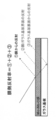
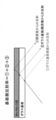
- the reflectance includes the reflectance of light incident from the thin film side (film-side reflectance) and the reflectance of light incident from the glass substrate side as illustrated in FIG. 2 (substrate-side reflection).
- the reflectance means only the film-side reflectance.
- the reflected light includes specular reflection light and diffuse reflection light. In the present disclosure, it means a relative total light reflectivity obtained by combining the specular reflection light and the diffuse reflection light.
- the oxide thin film according to the embodiment of the present invention also has an average transmittance for incident light in the visible light region (wavelength: 380 to 780 nm) when a thin film having a thickness of 100 ⁇ 10 nm is formed on a glass substrate. Is preferably 20% or less.
- the “average” transmittance is obtained by measuring the transmittance of the wavelength region every 5 nm and calculating the average value. With this level of reflectance and transmittance, light reflected from the metal wiring (copper foil or the like) inside the display or the panel can be sufficiently absorbed, and a reduction in visibility can be suppressed. Furthermore, the low reflectance required for the phase shift type photomask application can be satisfied.
- the transmittance is related to the thickness of the oxide thin film.
- the transmittance decreases as the thickness increases.
- the transmittance is specified when the thickness of the oxide thin film is 100 nm ⁇ 10 nm or more.
- ⁇ 10 nm means that 100 nm can be accurately formed.
- the film thickness fluctuates ⁇ 10 nm (that is, 90 to 110 nm)
- the fluctuation range of the transmittance is theoretically within ⁇ 1.3%.
- the oxide thin film according to the embodiment of the present invention satisfies the average transmittance of 20% or less even when the fluctuation range of the transmittance is taken into consideration.
- the oxide thin film according to the embodiment of the present invention preferably has a surface resistivity of 1.0 ⁇ 10 5 ⁇ / sq or less.
- the oxide thin film that functions as a light absorption film is stacked adjacent to the metal wiring to suppress light reflection by the metal wiring.
- the surface resistivity of the oxide thin film is preferably within the above range.
- the oxide thin film according to the embodiment of the present invention has excellent weather resistance, and the average transmittance and average reflectance change rate in the visible light region (wavelength: 380 to 780 nm) before and after the constant temperature and humidity test are 30% or less. It is preferable that Moreover, it is preferable that the change rate of the surface resistivity before and after a constant temperature and humidity test is 30% or less.
- the oxide thin film sample formed on the substrate is left in the room A (temperature 40 ° C.-humidity 90%) and the room B (temperature 85 ° C.-humidity 85%).
- the transmittance, reflectance, and surface resistivity after 120 hours, 500 hours, and 1000 hours were measured, and the rate of change was examined in comparison with each measured value immediately after film formation. It is.
- the thickness of the oxide thin film is preferably 20 to 2000 nm. If the film thickness is less than 20 nm, the light absorption ability may be lowered. On the other hand, if the film thickness exceeds 2000 nm, it takes more time than necessary to form the film. However, since the film thickness is finally determined by the device design, the film thickness is not limited to this film thickness as long as the light absorption ability can be secured.
- the oxide thin film according to the embodiment of the present invention is preferably amorphous. Since the amorphous film has a smaller film stress than the crystallized film, film peeling and cracking hardly occur at the time of lamination. Therefore, it is particularly suitable for use in flexible devices.
- the oxide sintered body according to the embodiment of the present invention includes Nb, Mo, and O (oxygen), and the content ratio (atomic ratio) of Nb and Mo is 0.1 ⁇ Nb / (Nb + Mo) ⁇ 0.8, The content ratio (atomic ratio) of O and metal (Nb + Mo) is 1.5 ⁇ O / (Nb + Mo) ⁇ 2.1, the XRD peak intensity I MoO2 belonging to the ( ⁇ 111) plane of the MoO 2 phase, and the background intensity relationship between I BG, characterized in that satisfy I MoO2 / I BG> 3.
- An oxide sintered body having such characteristics can be used as a sputtering target.
- the oxide sintered body according to the embodiment of the present invention satisfying the composition range of 0.1 ⁇ Nb / (Nb + Mo) ⁇ 0.8 and 1.5 ⁇ O / (Nb + Mo) ⁇ 2.1 is formed by sputtering.
- the formed thin film has desired optical characteristics, film resistance, and amorphous properties.
- the oxide sintered body when the content ratio of O and metal (Nb + Mo) is 1.5 ⁇ O / (Nb + Mo) ⁇ 2.1, the oxide sintered body (sputtering target) is used to form a sputter film.
- the content ratio of O and metal (Nb + Mo) is in the range of 1.5 ⁇ O / (Nb + Mo) ⁇ 2.0, and the desired film characteristics are obtained. can get.
- the oxide sintered body according to the embodiment of the present invention the XRD peak intensity I Mo02 attributable to (-111) plane of the MoO 2 phase, the relationship between the background intensity I BG, I MoO2 / I BG > 3 but satisfies the, satisfies the XRD peak intensity ratio I MoO2 / I BG> 3, molybdenum in the sintered body (Mo) is present most part as MoO 2, such oxidation When a sintered product is used, desired optical characteristics can be obtained in a sputtered thin film.
- the oxide sintered body according to the embodiment of the present invention preferably has a relative density of 80% or more. If the relative density is 80% or more, it can withstand practical use as a sputtering target. More preferably, it is 85% or more.
- the oxide sintered body according to the embodiment of the present invention preferably has a bulk resistivity of 100 m ⁇ ⁇ cm or less. Due to the decrease in bulk resistivity, film formation by DC sputtering becomes possible. Compared with RF sputtering, DC sputtering has a higher film formation rate and superior sputtering efficiency, and can improve throughput. Note that RF sputtering may be performed depending on manufacturing conditions, but even in that case, the film formation rate is improved.
- the oxide sintered body according to the embodiment of the present invention can be produced, for example, as follows.
- the raw material powders of NbO 2 powder and MoO 2 powder are weighed and mixed so as to have a desired composition.
- the raw material powder preferably has a purity of 99.9% or more and a particle diameter (D50) of 0.5 to 10 ⁇ m.
- D50 particle diameter
- As a mixing method it is preferable to use a ball mill or the like for pulverization.
- As raw powder it is conceivable to use a Nb 2 O 5 powder and Mo powder, and Nb 2 O 5 and Mo since the sintering temperature is significantly different, it is difficult to densify.
- the oxide sintered compact which consists of Nb, Mo, and O with a relative density of 80% or more can be obtained. Further, the obtained oxide sintered body can be processed into a sputtering target by cutting, polishing, or the like.
- the oxide thin film according to the embodiment of the present invention can be produced, for example, as follows.
- An NbO 2 sputtering target and a MoO 2 sputtering target are set in a sputtering apparatus, and simultaneous sputtering is performed to form a mixed film of NbO 2 and MoO 2 on the substrate.
- the film composition can be changed by changing each sputtering power at the time of sputtering.
- the sputtering target manufactured by the above-described method is placed in a sputtering apparatus, and sputtering is performed to form a mixed film of NbO 2 and MoO 2 on the substrate.
- the composition of the sputtering target is not completely the same as the composition of the film, but the composition approximates that. Since the composition of the target and the composition of the film are related, it is possible to grasp the composition of the target that can obtain the desired film composition by setting the conditions. In addition, the amount of oxygen in the film can be adjusted by adjusting the flow rate of oxygen introduced during sputtering.
- the evaluation method of the oxide thin film and the oxide sintered body according to the embodiment of the present invention is as follows, including examples and comparative examples.
- Apparatus Spectrophotometer UV-2450 manufactured by SHIMADZU Measurement sample: A sample formed with a film thickness of 100 ⁇ 10 nm on a glass substrate having a thickness of 0.7 mm, and an undeposited glass substrate
- Measurement sample A sample formed with a film thickness of 100 ⁇ 10 nm on a glass substrate having a thickness of 0.7 mm, and an undeposited glass substrate
- Measuring method (Reflectance) Relative total light reflectance using an integrating sphere (reference sample; specular mirror).
- the reflectance of light incident from the thin film side includes not only the reflectance from the thin film surface but also the reflectance from the glass substrate (front surface) at the interface with the thin film, from the back surface of the glass substrate. Includes reflectance.
- the reflectance of light incident from the glass substrate side is It includes the reflectance from the glass substrate surface and the reflectance from the thin film at the interface with the glass substrate. (Transmittance) Relative transmittance using a glass substrate as a reference sample.
- Judgment was made by the presence or absence of a diffraction peak by X-ray diffraction of the film formation sample.
- a diffraction peak due to the film material is not observed in the measurement under the following conditions, it is determined as an amorphous film.
- a case where I max / I BG ⁇ 5 is satisfied is indicated by ⁇ , and a case where it is not satisfied is indicated by ⁇ .
- Device Rigaku Smart Lab Tube: Cu-K ⁇ line Tube voltage: 40 kV Current: 30mA Measuring method: 2 ⁇ - ⁇ reflection method Scanning speed: 20 ° / min Sampling interval: 0.02 ° Measurement range: 10 ° -60 ° Measurement sample: film formation sample on glass substrate (EagleXG) (film thickness of 100 nm or more)
- Stylus type step meter Veeco Dektak8 Method The film thickness is measured from the level difference between the film-formed surface and the non-film-formed surface of the formed glass substrate.
- etching solution a hydrogen peroxide (H 2 O 2 ) -based chemical solution was used.
- H 2 O 2 hydrogen peroxide
- I MoO2 I MoO2' / I MoO2 -BG I MoO2 ′ : XRD peak intensity in the range of 25.5 ° ⁇ 2 ⁇ ⁇ 26.5 °
- I MoO2 -BG XRD average intensity in the range of 19.5 ° ⁇ 2 ⁇ ⁇ 20.5 °.
- Examples 1-1 to 1-6, Comparative Examples 1-1 to 1-2 NbO 2 target ( ⁇ 6 inch) and MoO 2 target ( ⁇ 6 inch) are installed in a sputtering device (ANELVA SPL-500), and a mixed film of NbO 2 and MoO 2 is formed on a glass substrate (EagleXG, ⁇ 4 inch) by simultaneous sputtering. did.
- the film formation conditions were as described above, and as shown in Table 1, the power of each target at the time of sputtering was changed to produce films having the compositions shown in Table 1.
- the MoO 2 film was formed by sputtering only the MoO 2 target.
- the NbO 2 film was formed by sputtering only the NbO 2 target. It is a film. Thereafter, the transmittance, surface reflectance / back reflectance, and surface resistivity immediately after film formation (room temperature) were measured for each oxide thin film with each composition changed, and etching properties were further investigated. The results are shown in Table 1.
- each oxide thin film formed on the substrate under the respective conditions was subjected to room A (temperature 40 ° C.-humidity 90%) and room B (temperature 85 ° C.-humidity 85%). Then, after 12 hours, 500 hours, and 1000 hours, changes in transmittance, surface reflectance / back reflectance, and surface resistance were examined. The results are shown in Table 2.
- the oxide thin films (Examples 1-2 to 1-5) all have 30% or less of change over time in the transmittance, reflectance, and surface resistance (change rate), and are weather resistant. It was an excellent film.
- the oxide thin film containing only Mo (Comparative Example 1-1) was inferior in weather resistance, and the transmittance and the like increased remarkably with the passage of time.
- the oxide thin film containing only Nb (Comparative Example 1-3) was hardly dissolved in the etching solution.
- Example 2-1 to 2-4 Comparative Example 2-1
- NbO 2 powder and MoO 2 powder having a purity of 99.9% or more and a particle size of 0.5 to 10 ⁇ m were prepared, and these powders were weighed so as to have the predetermined ratios shown in Table 3, The mixing and pulverization were carried out. Next, the obtained mixed powder was hot press sintered in an argon atmosphere at a sintering temperature of 1200 ° C. and a surface pressure of 250 kgf / cm 2 to prepare an oxide sintered body. Note that mixing, pulverization, and sintering were performed under the same conditions except that only the weighing ratio was adjusted. Table 3 shows the evaluation results of the obtained oxide sintered body.
- the relationship between the XRD peak intensity I Mo02 and background intensity I BG attributable to (-111) plane of the MoO 2 phase satisfies the I MoO2 / I BG> 3 either embodiment,
- the relative density was 80% or more, and the bulk resistivity was 100 m ⁇ cm or less.
- Comparative Example 2-1 the XRD peak intensity ratio of the MoO 2 phase was 1.7, and MoO 2 disappeared.
- the oxide sintered bodies obtained in Examples and Comparative Examples were processed into a sputtering target, and sputtering film formation was performed using the target.
- Table 3 shows the optical characteristics of the obtained sputtered film.
- the films formed by sputtering using the oxide sintered body obtained in the examples all had low average transmittance and average reflectance, and exhibited excellent light absorption ability.
- the oxide thin film according to the embodiment of the present invention has low transmittance and reflectance, has excellent light absorption ability, and can be processed by etching, has high weather resistance, and hardly changes over time. It has excellent characteristics. Moreover, since the oxide sintered body according to the embodiment of the present invention has a high density, it can be used as a sputtering target.
- An oxide thin film according to an embodiment of the present invention is used as a light absorption film for preventing reflection of light by a metal wiring used in a liquid crystal display, a plasma display, an organic EL display, a touch panel, a solar cell, and the like, and a photomask. It is very useful for materials and decoration.
Landscapes
- Chemical & Material Sciences (AREA)
- Organic Chemistry (AREA)
- Engineering & Computer Science (AREA)
- Materials Engineering (AREA)
- Mechanical Engineering (AREA)
- Metallurgy (AREA)
- Chemical Kinetics & Catalysis (AREA)
- Ceramic Engineering (AREA)
- Inorganic Chemistry (AREA)
- Manufacturing & Machinery (AREA)
- Structural Engineering (AREA)
- Physical Vapour Deposition (AREA)
- Inorganic Compounds Of Heavy Metals (AREA)
- Electroluminescent Light Sources (AREA)
- Compositions Of Oxide Ceramics (AREA)
Abstract
Description
また、本発明の実施形態に酸化物焼結体は、Nb、Mo、O(酸素)からなり、NbとMoの含有比率(原子比)が0.1≦Nb/(Nb+Mo)≦0.8、Oとメタル(Nb+Mo)の含有比率(原子比)が1.5<O/(Nb+Mo)<2.1、MoO2相の(-111)面に帰属するXRDピーク強度IMoO2とバックグラウンド強度IBGとの関係がIMoO2/IBG>3を満たす、ところに要旨を有する。
反射率には、図1に示すような、薄膜側から入射した光の反射率(膜側反射率)と、図2に示すような、ガラス基板側から入射した光の反射率(基板側反射率)とがあるが、本開示では、反射率は、膜側反射率のみを意味する。また、反射光には、鏡面反射光と拡散反射光とがあるが、本開示では、鏡面反射光と拡散反射光とを合わせた相対全光線反射率を意味する。
このレベルの反射率及び透過率であれば、ディスプレイやパネル内部における金属配線(銅箔等)から反射された光を十分に吸収することができ、視認性の低下を抑制することができる。さらには、位相シフト型フォトマスク用途として求められる低い反射率を満たすことができる。
ここで、本開示における恒温恒湿試験は、基板上に成膜した酸化物薄膜サンプルを、室内A(温度40℃-湿度90%)、室内B(温度85℃-湿度85%)に放置して、120時間経過後、500時間経過後及び1000時間経過後の、透過率、反射率及び表面抵抗率を測定し、成膜直後の各測定値と対比して、その変化率を調べたものである。
本発明の実施形態に係る酸化物焼結体は、Nb、Mo、O(酸素)からなり、NbとMoの含有比率(原子比)が0.1≦Nb/(Nb+Mo)≦0.8、Oとメタル(Nb+Mo)の含有比率(原子比)が1.5<O/(Nb+Mo)<2.1、MoO2相の(-111)面に帰属するXRDピーク強度IMoO2と、バックグラウンド強度IBGとの関係が、IMoO2/IBG>3を満たすことを特徴とする。このような特性を備えた酸化物焼結体は、スパッタリングターゲットとして使用することができる。
また、本発明の実施形態に係る酸化物焼結体は、バルク抵抗率が100mΩ・cm以下であることが好ましい。バルク抵抗率の低下により、DCスパッタによる成膜が可能となる。DCスパッタリングはRFスパッタリングに比べて、成膜速度が速く、スパッタ効率が優れており、スループットを向上できる。なお、製造条件によってはRFスパッタリングを行うことも場合もあるが、その場合でも、成膜速度の向上がある。
NbO2粉末、MoO2粉末の原料粉末を所望の組成となるように、秤量、混合する。原料粉末は純度が99.9%以上、粒子径(D50)が0.5~10μmのものを使用することが好ましい。混合方法としては、ボールミルなどを用いて粉砕を兼ねて、混合することが好ましい。原料粉として、Nb2O5粉末とMo粉末を使用することも考えられるが、Nb2O5とMoとは焼結温度が大きく異なることから、高密度化が困難である。
次に、混合粉末をAr雰囲気中、1100℃以上1200℃以下、加圧力250MPa以上、5~10時間、ホットプレス(一軸加圧焼結)を行う。これにより、相対密度80%以上のNb、Mo、Oからなる酸化物焼結体を得ることができる。また、得られた酸化物焼結体を切削、研磨などして、スパッタリングターゲットに加工することができる。
NbO2スパッタリングターゲット、MoO2スパッタリングターゲットをスパッタ装置に設置し、同時スパッタを行って、基板上にNbO2とMoO2の混合膜を成膜する。このとき、スパッタ時のそれぞれのスパッタパワーを変化させることで、膜組成を変えることができる。
又は、上述した方法によって作製されたスパッタリングターゲットをスパッタ装置に設置し、スパッタを実施して、基板上にNbO2とMoO2の混合膜を成膜する。このとき、スパッタリングターゲットの組成は、膜の組成と完全に同一となることはないが、それに近似した組成となる。ターゲットの組成と膜の組成とは関係性があるので、条件出しを行って所望の膜組成を得ることができるターゲットの組成を把握することが可能となる。また、スパッタ時に導入する酸素流量を調整することで、膜中の酸素量を調整することもできる。
<成膜条件>
スパッタ装置:ANELVA SPL-500
基板温度:室温(基板無加熱)
成膜雰囲気:Ar またはAr+O2
ガス圧:0.2~2.0Pa
ガス流量:50~100sccm
パワー:100~1000W(DC、RF)
基板:コーニング製 EagleXG(φ4mm×0.7mm)
(透過率、反射率について)
装置:SHIMADZU社製 分光光度計 UV-2450
測定サンプル:
厚さ0.7mmのガラス基板上に、膜厚100±10nmで成膜したサンプル、及び、未成膜ガラス基板
測定方法:
(反射率)積分球(基準サンプル;鏡面ミラー)を用いた相対全光線反射率。
薄膜側から入射した光の反射率(膜側反射率)には、薄膜面からの反射率だけでなく、薄膜との界面にあるガラス基板(表面)からの反射率、ガラス基板の裏面からの反射率を含む。
ガラス基板側から入射した光の反射率(基板側反射率)には、
ガラス基板面からの反射率とガラス基板との界面にある薄膜からの反射
率を含む。
(透過率)基準サンプルにガラス基板を使用した、相対透過率。
装置:JEOL製JXA-8500F
方法:EPMA(電子線マイクロアナライザー)
加速電圧:5~10keV
照射電流:1.0×10⁻⁸~1.0~10-9A
プローブ径10μmで、5点、ゴミの付着がなく、基板面がみえていない、平滑な成膜部分を選択し、点分析を行い、それらの平均組成を算出した。
装置:NPS社製 抵抗率測定器 Σ-5+
方法:直流4探針法
成膜サンプルのX線回折による回折ピークの有無で判断した。下記条件での測定にて膜材料に起因する回折ピークが見られない場合、アモルファス膜と判断する。ここで、回折ピークが存在しないとは、2θ=10°~60°における最大ピーク強度をImax、2θ=20°~25°の平均ピーク強度をIBGとしたときに、Imax/IBG < 5 である場合を意味する。また、表において、アモルファス性の判定基準として、Imax/IBG < 5を満たす場合を○、満たさない場合を×とした。
装置:リガク社製 Smart Lab
管球:Cu-Kα線
管電圧:40kV
電流:30mA
測定方法:2θ-θ反射法
スキャン速度:20°/min
サンプリング間隔:0.02°
測定範囲:10°~60°
測定サンプル:ガラス基板(EagleXG)上の成膜サンプル(膜厚100nm以上)
触針式段差計 Veeco製 Dektak8
方法;成膜されたガラス基板の成膜面と未成膜面の段差から膜厚を測定。
エッチング液は過酸化水素(H2O2)系の薬液を用いた。エッチング判定は、エッチングレートが速い場合を○、遅い場合を△、ほとんど溶けない場合を×とした。
装置:SII社製SPS3500DD
方法:ICP-OES(高周波誘導結合プラズマ発光分析法)
焼結体の寸法(ノギスを使用)と重量を測定して寸法密度を算出し、その寸法密度と焼結体の理論密度から、相対密度(%)=寸法密度/理論密度×100を算出する。
理論密度は、各酸化物の配合比とそれぞれの理論密度から計算する。
NbO2重量をa(wt%)、MoO2重量をb(wt%)としたとき、
理論密度=100/(a/5.90+b/6.44)
NbO2の理論密度:5.90g/cm3、MoO2の理論密度:6.44g/cm3
装置:リガク社製 Smart Lab
管球:Cu-Kα線
管電圧:40kV
電流:30mA
測定方法:2θ-θ反射法
スキャン速度:20°/min
サンプリング間隔:0.02°
測定範囲:10°~60°
サンプル測定箇所:スパッタ面
なおMoO2相の(-1 1 1)面に帰属するXRDピークIMoO2を以下に定義する。
IMoO2=IMoO2´/IMoO2-BG
IMoO2´:25.5°≦2θ≦26.5°の範囲におけるXRDピーク強度
IMoO2-BG:19.5°≦2θ<20.5°の範囲におけるXRD平均強度。
装置:NPS社製 抵抗率測定器 Σ-5+
方法:直流4探針法
NbO2ターゲット(φ6inch)とMoO2ターゲット(φ6inch)をスパッタ装置(ANELVA SPL-500)に設置して、同時スパッタによって、ガラス基板(EagleXG,φ4inch)上にNbO2とMoO2の混合膜を形成した。成膜条件は上述の通りとし、表1の通り、スパッタ時のそれぞれのターゲットのパワーを変化させて、表1記載の組成の膜を作製した。なお、比較例1-1は、MoO2ターゲットのみをスパッタして、MoO2膜を成膜したものであり、比較例1-2は、NbO2ターゲットのみをスパッタして、NbO2膜を成膜したものである。その後、組成をそれぞれ変化させた各酸化物薄膜について、成膜直後(室温)における透過率、表反射率・裏反射率、及び表面抵抗率を測定し、さらにエッチング性について調べた。その結果を表1に示す。

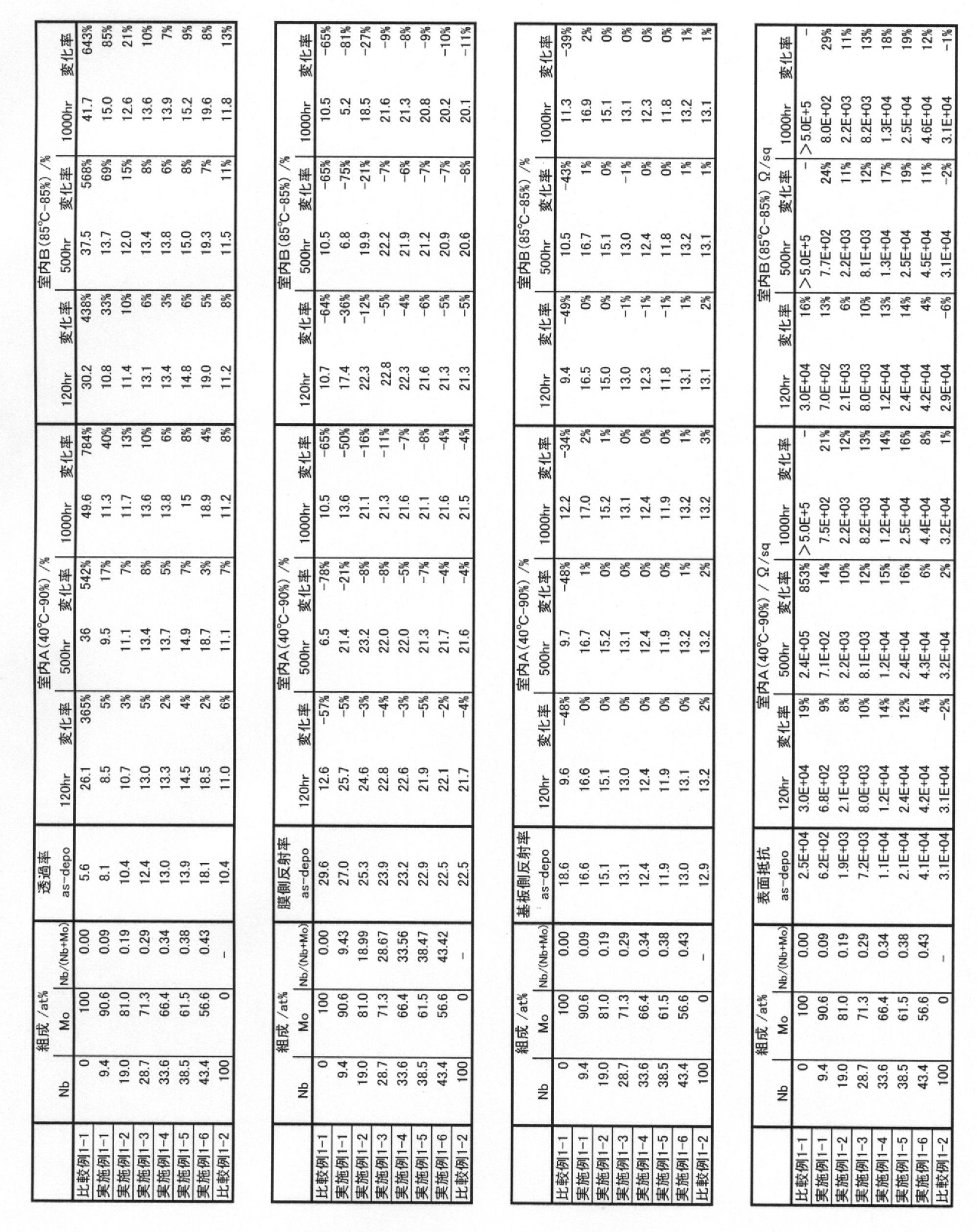
一方、Moのみを含有する酸化物薄膜(比較例1-1)は、耐候性が劣るものであり、時間の経過に伴い、透過率等が著しく上昇した。また、Nbのみを含有する酸化物薄膜(比較例1-3)は、エッチング液にほとんど溶けなかった。
原料粉末として、純度99.9%以上、粒径0.5~10μmのNbO2粉とMoO2粉を準備し、これらの粉末を表3に記載する所定の比率となるように秤量し、ボールミルによる混合・粉砕を実施した。次に、得られた混合粉末をアルゴン雰囲気中、焼結温度1200℃、面圧250kgf/cm2にてホットプレス焼結して、酸化物焼結体を作製した。なお、秤量比のみを調整した以外、いずれも同様の条件で混合・粉砕、焼結を実施した。 得られた酸化物焼結体の評価結果を表3に示す。表3に示されるように、いずれの実施例もMoO2相の(-111)面に帰属するXRDピーク強度IMoO2とバックグラウンド強度IBGとの関係がIMoO2/IBG>3を満たし、また、相対密度が80%以上であり、バルク抵抗率は100mΩcm以下であった。一方、比較例2-1については、MoO2相のXRDピーク強度比が1.7であり、MoO2が消失していた。
次に、実施例、比較例で得られた酸化物焼結体をスパッタリングターゲットに加工し、該ターゲットを用いてスパッタ成膜した。得られたスパッタ膜の光学特性を表3に示す。実施例で得られた酸化物焼結体を用いてスパッタ成膜した膜は、いずれも平均透過率及び平均反射率が低く、優れた光吸収能を示した。

Claims (12)
- Nb、Mo、Oからなる酸化物薄膜であって、NbとMoの含有比率(原子比)が0.1≦Nb/(Nb+Mo)≦0.8、Oとメタル(Mb+Mo)の含有比率(原子比)が1.5<O/(Nb+Mo)<2.0であることを特徴とする酸化物薄膜。
- 可視光域(波長:380~780nm)における平均反射率が30%以下であることを特徴とする請求項1記載の酸化物薄膜。
- 可視光域(波長:380~780nm)における平均透過率が20%以下であることを特徴とする請求項1又は2記載の酸化物薄膜。
- 表面抵抗率が1.0×10⁵Ω/sq以下であることを特徴とする請求項1~3のいずれか一項に記載の酸化物薄膜。
- 恒温恒湿試験前後の可視光域(波長:380~780nm)における平均反射率の変化率が30%以下であることを特徴とする請求項1~4のいずれか一項に記載の酸化物薄膜。
- 恒温恒湿試験前後の可視光域(波長:380~780nm)における平均透過率の変化率が30%以下であることを特徴とする請求項1~5のいずれか一項に記載の酸化物薄膜。
- 恒温恒湿試験前後の表面抵抗率の変化率が30%以下であることを特徴とする請求項1~6のいずれか一項に記載の酸化物薄膜。
- 膜厚が20~2000nmであることを特徴とする請求項1~7のいずれか一項に記載の酸化物薄膜。
- アモルファスであることを特徴とする請求項1~8のいずれか一項に記載の酸化物薄膜。
- Nb、Mo、Oからなる酸化物焼結体であって、NbとMoの含有比率(原子比)が0.1≦Nb/(Nb+Mo)≦0.8、Oとメタル(Mb+Mo)の含有比率(原子比)が1.5<O/(Nb+Mo)<2.1、MoO2相の(-111)面に帰属するXRDピーク強度IMoO2とバックグラウンド強度IBGとの関係がIMoO2/IBG>3を満たすことを特徴とする酸化物焼結体。
- 相対密度が80%以上であることを特徴とする請求項10記載の酸化物焼結体。
- バルク抵抗率が100mΩ・cm以下であることを特徴とする請求項10又は11に記載の酸化物焼結体。
Priority Applications (4)
| Application Number | Priority Date | Filing Date | Title |
|---|---|---|---|
| KR1020197027207A KR102225493B1 (ko) | 2018-03-13 | 2019-02-28 | 산화물 박막 및 당해 박막을 제조하기 위한 스퍼터링 타깃용 산화물 소결체 |
| CN201980002388.XA CN110637102B (zh) | 2018-03-13 | 2019-02-28 | 氧化物薄膜和用于制造该薄膜的溅射靶用氧化物烧结体 |
| JP2019528772A JP6767723B2 (ja) | 2018-03-13 | 2019-02-28 | 酸化物薄膜及び該薄膜を製造するためのスパッタリングターゲット用酸化物焼結体 |
| KR1020217004031A KR102315765B1 (ko) | 2018-03-13 | 2019-02-28 | 산화물 박막 및 당해 박막을 제조하기 위한 스퍼터링 타깃용 산화물 소결체 |
Applications Claiming Priority (2)
| Application Number | Priority Date | Filing Date | Title |
|---|---|---|---|
| JP2018045605 | 2018-03-13 | ||
| JP2018-045605 | 2018-03-13 |
Publications (1)
| Publication Number | Publication Date |
|---|---|
| WO2019176552A1 true WO2019176552A1 (ja) | 2019-09-19 |
Family
ID=67908233
Family Applications (1)
| Application Number | Title | Priority Date | Filing Date |
|---|---|---|---|
| PCT/JP2019/007733 Ceased WO2019176552A1 (ja) | 2018-03-13 | 2019-02-28 | 酸化物薄膜及び該薄膜を製造するためのスパッタリングターゲット用酸化物焼結体 |
Country Status (5)
| Country | Link |
|---|---|
| JP (1) | JP6767723B2 (ja) |
| KR (2) | KR102315765B1 (ja) |
| CN (1) | CN110637102B (ja) |
| TW (1) | TWI700382B (ja) |
| WO (1) | WO2019176552A1 (ja) |
Cited By (4)
| Publication number | Priority date | Publication date | Assignee | Title |
|---|---|---|---|---|
| WO2021125113A1 (ja) * | 2019-12-18 | 2021-06-24 | Agc株式会社 | 多層膜付き透明基体 |
| CN115925414A (zh) * | 2021-10-06 | 2023-04-07 | Lt金属株式会社 | 氧化钼基烧结体、使用该烧结体的薄膜、包含该薄膜的薄膜晶体管及显示装置 |
| JPWO2024202444A1 (ja) * | 2023-03-29 | 2024-10-03 | ||
| EP4299542A4 (en) * | 2021-02-26 | 2025-03-05 | Agc Inc. | TRANSPARENT SUBSTRATE WITH MULTILAYER FILM AND IMAGE DISPLAY DEVICE |
Families Citing this family (7)
| Publication number | Priority date | Publication date | Assignee | Title |
|---|---|---|---|---|
| CN114916228B (zh) * | 2020-12-10 | 2023-08-15 | Lt金属株式会社 | 以钼氧化物为主成分的金属氧化物烧结体及包含其的溅射靶材 |
| KR102315283B1 (ko) * | 2020-12-10 | 2021-10-21 | 엘티메탈 주식회사 | 몰리브덴 산화물을 주된 성분으로 하는 금속 산화물 박막 및 이러한 박막이 형성된 박막트랜지스터와 디스플레이 장치 |
| KR102315308B1 (ko) * | 2020-12-10 | 2021-10-21 | 엘티메탈 주식회사 | 몰리브덴 산화물을 주된 성분으로 하는 금속 산화물 소결체 및 이를 포함하는 스퍼터링 타겟 |
| KR102646917B1 (ko) * | 2021-09-16 | 2024-03-13 | 엘티메탈 주식회사 | 몰리브덴 산화물계 소결체, 상기 소결체를 이용한 박막, 상기 박막을 포함하는 박막트랜지스터 및 디스플레이 장치 |
| KR102917229B1 (ko) * | 2021-10-14 | 2026-01-28 | 엘티메탈 주식회사 | 몰리브덴 산화물계 소결체, 이를 포함하는 스퍼터링 타겟 및 산화물 박막 |
| CN118119575A (zh) * | 2021-10-14 | 2024-05-31 | Lt金属株式会社 | 钼氧化物基烧结体、包含其的溅射靶材以及氧化物薄膜 |
| PL247166B1 (pl) * | 2023-01-02 | 2025-05-26 | Instytut Masz Przeplywowych Im Roberta Szewalskiego Polskiej Akademii Nauk | Sposób wytwarzania warstw krystalicznych trójtlenku molibdenu |
Citations (3)
| Publication number | Priority date | Publication date | Assignee | Title |
|---|---|---|---|---|
| JP2000214309A (ja) * | 1999-01-25 | 2000-08-04 | Asahi Glass Co Ltd | ブラックマトリックス薄膜付き基板、カラ―フィルタ基板、ブラックマトリックス薄膜形成用タ―ゲットおよび基板の製造方法 |
| JP2000214308A (ja) * | 1999-01-25 | 2000-08-04 | Asahi Glass Co Ltd | ブラックマトリックス薄膜、多層ブラックマトリックス、カラ―フィルタ基板、ブラックマトリックス薄膜形成用タ―ゲットおよび基板の製造方法 |
| JP2016502592A (ja) * | 2012-10-23 | 2016-01-28 | ヘレーウス ドイチュラント ゲゼルシャフト ミット ベシュレンクテルハフツング ウント コンパニー コマンディートゲゼルシャフトHeraeus Deutschland GmbH&Co.KG | 光を吸収する層系及びその製造並びにそのために適したスパッタターゲット |
Family Cites Families (6)
| Publication number | Priority date | Publication date | Assignee | Title |
|---|---|---|---|---|
| EP0852266B1 (en) * | 1995-08-23 | 2004-10-13 | Asahi Glass Ceramics Co., Ltd. | Target, process for production thereof, and method of forming highly refractive film |
| JP2001073125A (ja) * | 1999-09-08 | 2001-03-21 | Nikko Materials Co Ltd | Co−Ta系合金スパッタリングターゲット及びその製造方法 |
| CN100558552C (zh) * | 2006-08-09 | 2009-11-11 | 株式会社神户制钢所 | 硬质皮膜及硬质皮膜被覆材 |
| DE102013103679A1 (de) | 2013-04-11 | 2014-10-30 | Heraeus Materials Technology Gmbh & Co. Kg | Licht absorbierende Schicht und die Schicht enthaltendes Schichtsystem, Verfahren zur dessen Herstellung und dafür geeignetes Sputtertarget |
| JP6394437B2 (ja) | 2015-02-27 | 2018-09-26 | 三菱マテリアル株式会社 | スパッタリングターゲット |
| JP6528597B2 (ja) | 2015-08-20 | 2019-06-12 | 住友金属鉱山株式会社 | 導電性基板、および導電性基板の製造方法 |
-
2019
- 2019-02-28 CN CN201980002388.XA patent/CN110637102B/zh active Active
- 2019-02-28 KR KR1020217004031A patent/KR102315765B1/ko active Active
- 2019-02-28 WO PCT/JP2019/007733 patent/WO2019176552A1/ja not_active Ceased
- 2019-02-28 KR KR1020197027207A patent/KR102225493B1/ko active Active
- 2019-02-28 JP JP2019528772A patent/JP6767723B2/ja active Active
- 2019-03-05 TW TW108107194A patent/TWI700382B/zh active
Patent Citations (4)
| Publication number | Priority date | Publication date | Assignee | Title |
|---|---|---|---|---|
| JP2000214309A (ja) * | 1999-01-25 | 2000-08-04 | Asahi Glass Co Ltd | ブラックマトリックス薄膜付き基板、カラ―フィルタ基板、ブラックマトリックス薄膜形成用タ―ゲットおよび基板の製造方法 |
| JP2000214308A (ja) * | 1999-01-25 | 2000-08-04 | Asahi Glass Co Ltd | ブラックマトリックス薄膜、多層ブラックマトリックス、カラ―フィルタ基板、ブラックマトリックス薄膜形成用タ―ゲットおよび基板の製造方法 |
| JP2016502592A (ja) * | 2012-10-23 | 2016-01-28 | ヘレーウス ドイチュラント ゲゼルシャフト ミット ベシュレンクテルハフツング ウント コンパニー コマンディートゲゼルシャフトHeraeus Deutschland GmbH&Co.KG | 光を吸収する層系及びその製造並びにそのために適したスパッタターゲット |
| JP2016504484A (ja) * | 2012-10-23 | 2016-02-12 | ヘレーウス ドイチュラント ゲゼルシャフト ミット ベシュレンクテルハフツング ウント コンパニー コマンディートゲゼルシャフトHeraeus Deutschland GmbH&Co.KG | 高吸収性層系、この層系の製造方法及びこのために適したスパッタターゲット |
Non-Patent Citations (1)
| Title |
|---|
| MURPHY, NEIL R. ET AL.: "Hybrid co-deposition of molybdenum doped niobium pentoxide (NbxMoyOz) thin films", JOURNAL OF ALLOYS AND COMPOUNDS, vol. 681, 2016, pages 350 - 358, XP029552871, doi:10.1016/j.jallcom.2016.04.233 * |
Cited By (10)
| Publication number | Priority date | Publication date | Assignee | Title |
|---|---|---|---|---|
| WO2021125113A1 (ja) * | 2019-12-18 | 2021-06-24 | Agc株式会社 | 多層膜付き透明基体 |
| JPWO2021125113A1 (ja) * | 2019-12-18 | 2021-06-24 | ||
| JP7156556B2 (ja) | 2019-12-18 | 2022-10-19 | Agc株式会社 | 多層膜付き透明基体 |
| EP4299542A4 (en) * | 2021-02-26 | 2025-03-05 | Agc Inc. | TRANSPARENT SUBSTRATE WITH MULTILAYER FILM AND IMAGE DISPLAY DEVICE |
| CN115925414A (zh) * | 2021-10-06 | 2023-04-07 | Lt金属株式会社 | 氧化钼基烧结体、使用该烧结体的薄膜、包含该薄膜的薄膜晶体管及显示装置 |
| CN115925414B (zh) * | 2021-10-06 | 2024-04-23 | Lt金属株式会社 | 氧化钼基烧结体、使用该烧结体的薄膜、包含该薄膜的薄膜晶体管及显示装置 |
| JPWO2024202444A1 (ja) * | 2023-03-29 | 2024-10-03 | ||
| WO2024202444A1 (ja) * | 2023-03-29 | 2024-10-03 | Jx金属株式会社 | 酸化物スパッタリングターゲット及び酸化物膜 |
| KR20250145651A (ko) | 2023-03-29 | 2025-10-13 | 제이엑스금속주식회사 | 산화물 스퍼터링 타깃 및 산화물막 |
| JP7761813B2 (ja) | 2023-03-29 | 2025-10-28 | Jx金属株式会社 | 酸化物スパッタリングターゲット及び酸化物膜 |
Also Published As
| Publication number | Publication date |
|---|---|
| KR102225493B1 (ko) | 2021-03-10 |
| CN110637102A (zh) | 2019-12-31 |
| TW201938823A (zh) | 2019-10-01 |
| TWI700382B (zh) | 2020-08-01 |
| KR102315765B1 (ko) | 2021-10-22 |
| JPWO2019176552A1 (ja) | 2020-04-16 |
| JP6767723B2 (ja) | 2020-10-14 |
| KR20210019126A (ko) | 2021-02-19 |
| CN110637102B (zh) | 2021-08-20 |
| KR20190120272A (ko) | 2019-10-23 |
Similar Documents
| Publication | Publication Date | Title |
|---|---|---|
| JP6767723B2 (ja) | 酸化物薄膜及び該薄膜を製造するためのスパッタリングターゲット用酸化物焼結体 | |
| TWI506154B (zh) | 吸光層系統,彼之製法以及適合彼所用之濺射靶材 | |
| CN105143931B (zh) | 光吸收层及含该层层系统、层系统制造方法及适用溅镀靶 | |
| TWI525060B (zh) | An oxide sintered body, a sputtering target, a thin film, and an oxide sintered body | |
| JP2007277075A (ja) | 酸化物焼結体、その製造方法、それを用いた透明導電膜の製造方法、及び得られる透明導電膜 | |
| JP5735190B1 (ja) | 酸化物焼結体、スパッタリングターゲット及び酸化物薄膜 | |
| CN112119179A (zh) | 层叠膜及Ag合金溅射靶 | |
| CN115819083B (zh) | 氧化钼基烧结体、使用该烧结体的薄膜、包含该薄膜的薄膜晶体管及显示装置 | |
| JP5392633B2 (ja) | ZnO系透明導電膜用ターゲットおよびその製造方法 | |
| JP7761813B2 (ja) | 酸化物スパッタリングターゲット及び酸化物膜 | |
| WO2014168073A1 (ja) | 酸化物スパッタリングターゲット、その製造方法及び光記録媒体用保護膜 | |
| JP4779798B2 (ja) | 酸化物焼結体、ターゲット、およびそれを用いて得られる透明導電膜 | |
| JP2007314812A (ja) | スパッタリングターゲットおよび成膜方法 | |
| JP4763962B2 (ja) | 酸化膜形成用スパッタリングターゲットとそれを用いた酸化膜の製造方法 | |
| CN112424390A (zh) | 光学功能膜、溅射靶及溅射靶的制造方法 | |
| JP5968462B2 (ja) | 酸化物焼結体、酸化物スパッタリングターゲット及び高屈折率の導電性酸化物薄膜並びに酸化物焼結体の製造方法 | |
| WO2021241687A1 (ja) | スパッタリングターゲット、および、光学機能膜 | |
| WO2020050421A1 (ja) | 光学機能膜、スパッタリングターゲット、及び、スパッタリングターゲットの製造方法 | |
| WO2022097635A1 (ja) | スパッタリングターゲット、スパッタリングターゲットの製造方法、および、光学機能膜 |
Legal Events
| Date | Code | Title | Description |
|---|---|---|---|
| ENP | Entry into the national phase |
Ref document number: 2019528772 Country of ref document: JP Kind code of ref document: A |
|
| ENP | Entry into the national phase |
Ref document number: 20197027207 Country of ref document: KR Kind code of ref document: A |
|
| 121 | Ep: the epo has been informed by wipo that ep was designated in this application |
Ref document number: 19766958 Country of ref document: EP Kind code of ref document: A1 |
|
| NENP | Non-entry into the national phase |
Ref country code: DE |
|
| 122 | Ep: pct application non-entry in european phase |
Ref document number: 19766958 Country of ref document: EP Kind code of ref document: A1 |