WO2019176129A1 - 半導体装置 - Google Patents
半導体装置 Download PDFInfo
- Publication number
- WO2019176129A1 WO2019176129A1 PCT/JP2018/029629 JP2018029629W WO2019176129A1 WO 2019176129 A1 WO2019176129 A1 WO 2019176129A1 JP 2018029629 W JP2018029629 W JP 2018029629W WO 2019176129 A1 WO2019176129 A1 WO 2019176129A1
- Authority
- WO
- WIPO (PCT)
- Prior art keywords
- electrode plate
- layer
- expansion coefficient
- linear expansion
- cooler
- Prior art date
- Legal status (The legal status is an assumption and is not a legal conclusion. Google has not performed a legal analysis and makes no representation as to the accuracy of the status listed.)
- Ceased
Links
Images




Classifications
-
- H—ELECTRICITY
- H10—SEMICONDUCTOR DEVICES; ELECTRIC SOLID-STATE DEVICES NOT OTHERWISE PROVIDED FOR
- H10W—GENERIC PACKAGES, INTERCONNECTIONS, CONNECTORS OR OTHER CONSTRUCTIONAL DETAILS OF DEVICES COVERED BY CLASS H10
- H10W40/00—Arrangements for thermal protection or thermal control
- H10W40/10—Arrangements for heating
-
- H—ELECTRICITY
- H10—SEMICONDUCTOR DEVICES; ELECTRIC SOLID-STATE DEVICES NOT OTHERWISE PROVIDED FOR
- H10W—GENERIC PACKAGES, INTERCONNECTIONS, CONNECTORS OR OTHER CONSTRUCTIONAL DETAILS OF DEVICES COVERED BY CLASS H10
- H10W40/00—Arrangements for thermal protection or thermal control
- H10W40/60—Securing means for detachable heating or cooling arrangements, e.g. clamps
-
- H—ELECTRICITY
- H10—SEMICONDUCTOR DEVICES; ELECTRIC SOLID-STATE DEVICES NOT OTHERWISE PROVIDED FOR
- H10W—GENERIC PACKAGES, INTERCONNECTIONS, CONNECTORS OR OTHER CONSTRUCTIONAL DETAILS OF DEVICES COVERED BY CLASS H10
- H10W74/00—Encapsulations, e.g. protective coatings
- H10W74/40—Encapsulations, e.g. protective coatings characterised by their materials
-
- H—ELECTRICITY
- H10—SEMICONDUCTOR DEVICES; ELECTRIC SOLID-STATE DEVICES NOT OTHERWISE PROVIDED FOR
- H10W—GENERIC PACKAGES, INTERCONNECTIONS, CONNECTORS OR OTHER CONSTRUCTIONAL DETAILS OF DEVICES COVERED BY CLASS H10
- H10W90/00—Package configurations
-
- H—ELECTRICITY
- H10—SEMICONDUCTOR DEVICES; ELECTRIC SOLID-STATE DEVICES NOT OTHERWISE PROVIDED FOR
- H10W—GENERIC PACKAGES, INTERCONNECTIONS, CONNECTORS OR OTHER CONSTRUCTIONAL DETAILS OF DEVICES COVERED BY CLASS H10
- H10W72/00—Interconnections or connectors in packages
- H10W72/90—Bond pads, in general
- H10W72/921—Structures or relative sizes of bond pads
- H10W72/926—Multiple bond pads having different sizes
Definitions
- Embodiments relate to a semiconductor device.
- a plurality of semiconductor switching elements may be operated in parallel to suppress temperature rise.
- some power semiconductor modules have a plurality of switching elements connected in parallel mounted in a single package.
- Embodiments provide a semiconductor device with improved reliability.
- the semiconductor device is opposite to the first surface of the first electrode plate, the first electrode plate having a first surface and a second surface located on the back side of the first surface.
- a second electrode plate disposed, at least one semiconductor element disposed between the first electrode plate and the second electrode plate, and connected to the first electrode plate and the second electrode plate;
- a first cooler disposed opposite to the second surface of the first electrode plate;
- a first intermediate member disposed between the first electrode plate and the first cooler and joined to both; Is provided.
- the first intermediate member has a laminated structure including a first layer having a first linear expansion coefficient and a second layer having a second linear expansion coefficient, and the first layer includes the first electrode plate. And the second layer.
- the linear expansion coefficient of the material of the first electrode plate is closer to the first linear expansion coefficient than the second linear expansion coefficient, and the linear expansion coefficient of the material of the first cooler is greater than the first linear expansion coefficient. Is close to the second linear expansion coefficient.
- 1 is a schematic cross-sectional view showing a semiconductor device according to a first embodiment.
- 1 is a schematic diagram showing a horizontal cross section of a semiconductor device according to a first embodiment.
- 1 is a partial cross-sectional view schematically showing a semiconductor device according to a first embodiment.
- 1 is a perspective view schematically showing a semiconductor device according to a first embodiment.
- 1 is a schematic cross-sectional view showing a connection structure of a semiconductor device according to a first embodiment. It is a schematic cross section showing the characteristic of the semiconductor device concerning a 1st embodiment. It is a graph which shows the characteristic of the semiconductor device concerning a 1st embodiment. It is a schematic cross section which shows the semiconductor device which concerns on 2nd Embodiment. It is a fragmentary sectional view showing typically the semiconductor device concerning a 2nd embodiment. It is a fragmentary sectional view showing typically the semiconductor device concerning a comparative example.
- each part will be described using the X-axis, Y-axis, and Z-axis shown in each drawing.
- the X axis, the Y axis, and the Z axis are orthogonal to each other and represent the X direction, the Y direction, and the Z direction, respectively.
- the Z direction may be described as the upper side and the opposite direction as the lower side.
- FIG. 1 is a schematic cross-sectional view showing a semiconductor device 1 according to the first embodiment.
- the semiconductor device 1 is, for example, a power semiconductor module.
- the semiconductor device 1 includes a plurality of submodules 10 and a cooler 20.
- the submodule 10 is disposed on, for example, an aluminum cooler 20.
- the cooler 20 has a mount portion 23 connected to the submodule 10.
- the mount portion 23 is, for example, a protrusion protruding upward (Z direction), and is inserted into the opening on the lower surface side of the submodule 10.
- a resin member 37 is disposed between the opening of the submodule 10 and the mount portion 23, and the connection portion between the submodule 10 and the cooler 20 is sealed. The resin member 37 fills at least the opening of the submodule 10 and protects the joint between the submodule 10 and the cooler 20.
- Case 30 that covers the plurality of submodules 10 disposed on the upper surface of the cooler 20 is disposed.
- Case 30 includes a side wall 33 and a cover 35.
- the side wall 33 is provided so as to surround the plurality of submodules 10 and is connected to the cooler 20.
- the cover 35 covers the upper surfaces of the plurality of submodules 10.
- an epoxy resin is used as the material of the case 30.
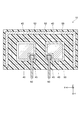
- FIG. 2 is a schematic diagram showing a horizontal section of the semiconductor device 1 according to the first embodiment.
- FIG. 2 is a schematic diagram showing a horizontal cross section of the submodule 10, and shows a cross section along the line AA shown in FIG.
- the submodule 10 includes a semiconductor element 40.
- the semiconductor element 40 is mounted on the electrode plate 50 and sealed with a resin member 65. At least one semiconductor element 40 is disposed on the electrode plate 50. In this example, two semiconductor elements 40 are arranged.
- the semiconductor element 40 is, for example, a power semiconductor element used for power conversion.
- a power semiconductor element is, for example, a switching element having a control gate such as an IGBT (Insulated Gate Bipolar Transistor) or a MOSFET (Metal Oxide Semiconductor Field Effect Effector) or a diode such as an FRD (Fast Recovery Diode).
- the semiconductor device 1 may incorporate both a submodule including a switching element and a submodule including a diode element. Moreover, both a switching element and a diode element may be mixed in one submodule.
- the semiconductor element 40 has, for example, a main electrode 43 and a gate electrode 45 on the upper surface thereof.
- the main electrode 43 is, for example, an emitter electrode or a source electrode, and is connected to an electrode plate 70 (see FIG. 3) disposed above.
- the collector electrode or drain electrode disposed on the back side of the semiconductor element 40 is connected to the electrode plate 50.
- a gate terminal 80 is bonded to the gate electrode 45.
- the submodule 10 includes a case 60 including a metal such as iron.
- the case 60 has higher rigidity than a resin member 65 described later, and is disposed so as to surround the semiconductor element 40, the electrode plate 50, and the electrode plate 70 (see FIG. 3).
- the case 60 affects another submodule 10 disposed around the case 60. It may have a function to prevent such explosive failure.
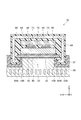
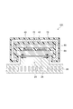
- FIG. 3 is a partial cross-sectional view schematically showing the semiconductor device 1 according to the first embodiment.
- FIG. 3 is a schematic diagram showing a cross-sectional structure of the submodule 10.
- the submodule 10 includes a semiconductor element 40, an electrode plate 50, an electrode plate 70, and a case 60.
- two semiconductor elements 40 are disposed between the electrode plate 50 and the electrode plate 70.
- the semiconductor element 40 is electrically connected to the electrode plate 50 and the electrode plate 70 via a bonding member (not shown).
- the electrode plate 70 has a plurality of convex portions 73.
- the plurality of convex portions 73 may be provided integrally with the electrode plate 70 or may be joined to the electrode plate 70.
- the convex portion 73 is connected to the main electrode 43 of the semiconductor element 40 via a connection member (not shown).
- the submodule 10 further includes an intermediate member 90.
- the intermediate member 90 is disposed between the cooler 20 and the electrode plate 50.
- the intermediate member 90 is a plate-like member having conductivity.
- the intermediate member 90 is a composite member having a structure in which a plurality of metal layers are stacked.
- the submodule 10 has, for example, a structure in which the semiconductor element 40, the electrode plate 50, the electrode plate 70, the case 60, and the intermediate member 90 are resin-molded.
- the case 60 is disposed so as to surround the semiconductor element 40, the electrode plate 50, the electrode plate 70, and the intermediate member 90, and has an opening 60B on the lower surface thereof.
- the opening 60 ⁇ / b> B has an opening area that is narrower than the lower surface of the intermediate member 90.
- the opening 60 ⁇ / b> B is located inside the outer edge of the intermediate member 90 when viewed in the Z direction.
- the submodule 10 is molded by the resin member 65.
- the resin member 65 is filled in the case 60 and covers the outer surface of the case 60.
- an opening 10 ⁇ / b> B is provided on the lower surface of the submodule 10.
- the opening 10 ⁇ / b> B is located inside the opening 60 ⁇ / b> B of the case 60.
- the opening 10B exposes the lower surface of the intermediate member 90 on the bottom surface.
- the submodule 10 is formed using, for example, vacuum forming.
- the resin member 65 is, for example, a thermosetting resin.
- the mount portion 23 of the cooler 20 is inserted into the opening 10B on the lower surface of the submodule 10 and joined to the intermediate member 90 via the joining member 25.
- the electrode plate 50 is joined to the intermediate member 90 via the joining member 55.
- the joining member 25 and the joining member 55 are, for example, solder materials.
- the bonding member 25 has a melting point lower than the melting point of the bonding member 55.
- Joule heat generated in the semiconductor element 40 is dissipated to the outside through the electrode plate 50, the intermediate member 90, and the cooler 20.
- the cooler 20 has a plurality of cavities 20S. For example, Joule heat generated in the semiconductor element 40 can be effectively dissipated by circulating the coolant in the cavity 20S.
- the resin member 37 is filled in the opening 10B in which the mount portion 23 of the cooler 20 is inserted.
- a connection portion between the cooler 20 and the intermediate member 90 is sealed with a resin member 37.
- the connecting portion between the electrode plate 50 and the intermediate member 90 is also sealed with the resin member 65.
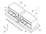
- FIG. 4 is a perspective view schematically showing the configuration of the semiconductor device 1 according to the first embodiment. As shown in FIG. 4, the plurality of submodules 10 are arranged on the upper surface of the cooler 20. In FIG. 4, the display of the case 30 surrounding the plurality of submodules 10 and the resin disposed therein is omitted.
- the case 60 has an opening on the side surface in the extending direction of the gate terminal 80.
- the gate terminal 80 is provided so as to extend from a resin member 65 (not shown) filled in the case 60.
- the electrode terminal 83 connected to the electrode plate 70 is also provided so as to extend in the same direction as the gate terminal 80.
- each submodule 10 is connected to the bus bar 87 via the connection conductor 85.
- the plurality of semiconductor elements 40 arranged between the electrode plate 50 and the electrode plate 70 can be connected in parallel between the cooler 20 and the bus bar 87.
- the positive electrode (not shown) of the semiconductor device 1 is electrically connected to the semiconductor element 40 via the cooler 20 and the electrode plate 50.
- the negative electrode (not shown) of the semiconductor device 1 is electrically connected to the semiconductor element 40 via the bus bar 87 and the electrode plate 70.
- the material of the electrode plate 50, the electrode plate 70, and the gate terminal 80 is, for example, a metal material containing copper or aluminum having high electrical conductivity and high thermal conductivity as a main component.
- the material of the cooler 20 is also a metal material containing copper or aluminum as a main component.
- the reliability can be improved by disposing the intermediate member 90 between the cooler 20 and the electrode plate 50.
- the intermediate member 90 is not disposed between the cooler 20 and the electrode plate 50, and the cooler 20 and the electrode plate 50 are joined via the joining member 25. Has been.
- the electrode plates 50 and 70 are preferably made of copper having a low electrical resistivity and a high thermal conductivity. As a result, the material of the cooler 20 and the material of the electrode plate 50 may be different.
- the thermal expansion of the cooler 20 made of aluminum is larger than that of the electrode plate 50 made of copper. Then, due to the thermal strain resulting from this difference, the bonding member 25 may deteriorate and affect the reliability of the semiconductor device 1.
- the thermal strain applied to the joining member 25 and the joining member 55 can be reduced by arranging the intermediate member 90. Thereby, the reliability of the semiconductor device 1 can be improved.
- FIG. 5 is a schematic cross-sectional view showing the connection structure of the semiconductor device 1 according to the first embodiment.
- FIG. 5 is a schematic diagram illustrating a connection structure between the cooler 20 and the intermediate member 90 and between the electrode plate 50 and the intermediate member 90.
- the intermediate member 90 is a plate-like member including at least two different metal layers.
- the intermediate member 90 includes, for example, a first layer 93 and a second layer 95.
- the first layer 93 is located between the electrode plate 50 and the second layer 95 and has a first layer thickness T1.
- the first layer 93 has a linear expansion coefficient that is closer to the linear expansion coefficient of the material of the electrode plate 50 than the linear expansion coefficient of the second layer 95.
- the second layer 95 is located between the mount portion 23 of the cooler 20 and the first layer 93 and has a second layer thickness T2.
- the second layer 95 has a linear expansion coefficient that is closer to the linear expansion coefficient of the material of the cooler 20 than the linear expansion coefficient of the first layer 93.
- the first layer 93 includes the same material as the electrode plate 50.
- the second layer 95 includes the same material as the cooler 20.
- the first layer 93 is, for example, a metal layer containing copper
- the second layer 95 is, for example, a metal layer containing aluminum.
- the intermediate member 90 can further include a third layer 97 positioned between the cooler 20 and the second layer 95, for example.
- a third layer 97 positioned between the cooler 20 and the second layer 95, for example.
- the third layer 97 is a metal layer containing copper, for example.
- the intermediate member 90 exposed in the opening 10 ⁇ / b> B (see FIG. 3) on the lower surface side of the submodule 10. It is preferable to remove the surface layer by, for example, mechanical processing. Thereby, an oxide film or dirt generated on the exposed surface of the intermediate member 90 in the process of forming the submodule 10 can be removed, and wettability of the intermediate member 90 to the bonding member 25 can be improved. As a result, the third layer thickness T3 of the third layer 97 that is in contact with the joining member 25 is thinner than the fourth layer thickness T4 of the peripheral portion covered with the resin member 65.
- a material having high wettability with respect to the joining member 25 for example, a plating layer of nickel or copper may be formed on the exposed surface of the intermediate member 90. Furthermore, it is preferable that the surface of the mount portion 23 of the cooler 20 is plated with a material having high wettability with respect to the bonding member 25. Thereby, the joint strength between the submodule 10 and the cooler 20 can be improved.
- FIG. 6 is a schematic cross-sectional view showing characteristics of the semiconductor device 1 according to the first embodiment.
- FIG. 6 is a schematic view illustrating the operation of the intermediate member 90 disposed between the cooler 20 and the electrode plate 50. The arrows shown in FIG. 6 schematically represent the thermal expansion of each member.
- the first layer 93 of the intermediate member 90 has substantially the same thermal expansion as that of the electrode plate 50. For this reason, thermal strain applied to the joining member 55 located between the electrode plate 50 and the first layer 93 can be reduced. Further, the first layer 93 has a first layer thickness T1 (see FIG. 5) that can suppress the influence of the thermal expansion of the second layer 95 on the bonding member 55.
- the second layer 95 of the intermediate member 90 has substantially the same thermal expansion as that of the cooler 20. For this reason, the thermal strain applied to the joining member 25 located between the cooler 20 and the second layer 95 can be reduced.
- the second layer 95 has a second layer thickness T ⁇ b> 2 that can suppress the influence of the thermal expansion of the first layer 93 on the bonding member 25.
- the third layer 97 has a third layer thickness T3 that does not hinder the effect of strain relaxation of the bonding member 25 by the second layer.
- the third layer thickness T3 is thinner than the second layer thickness T2 (see FIG. 5).
- the first layer thickness T1 is larger than the third layer thickness T3.
- the resin member 37 and the resin member 65 have different linear expansion coefficients.
- a material having a linear expansion coefficient that is close to the linear expansion coefficient of the material of the cooler 20 is used for the resin member 37 that covers the end portion of the joining member 25 positioned between the cooler 20 and the intermediate member 90.
- a material having a linear expansion coefficient that is close to the linear expansion coefficient of the material of the electrode plate 50 is used for the resin member 65 that covers the end of the bonding member 55 positioned between the electrode plate 50 and the intermediate member 90. .
- the resin member 37 a material having a linear expansion coefficient closer to that of aluminum than that of copper is used.
- the resin member 65 for example, a material having a linear expansion coefficient closer to that of copper than that of aluminum is used.
- the resin member 37 and the resin member 65 are, for example, an epoxy resin, and the resin member 37 is an epoxy resin having a composition different from that of the resin member 65.
- the joining member 25 is caused by a difference in linear expansion coefficient between the material of the cooler 20 and the material of the electrode plate 50. And the intermediate member 90 relieves the distortion (thermal deformation) of 55.
- the bonding member 25 located between the cooler 20 and the intermediate member 90 is sealed with the resin member 37
- the bonding member 55 between the electrode plate 50 and the intermediate member 90 is sealed with the resin member 65.
- thermal deformation of the joining members 25 and 55 can be effectively suppressed.
- the linear expansion coefficient of the resin member 37 is set to a value close to the linear expansion coefficient of the material of the cooler 20
- the linear expansion coefficient of the resin member 65 is set to a value close to the linear expansion coefficient of the material of the electrode plate 50.
- the distortion of the members 25 and 55 can be greatly suppressed.
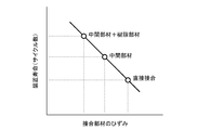
- FIG. 7 is a graph showing the characteristics of the semiconductor device 1 according to the first embodiment.
- FIG. 7 is a graph showing the relationship between the strain of the joining member and the lifetime of the semiconductor device 1.
- the horizontal axis represents the magnitude of strain of the joining member, and the vertical axis represents the device life represented by the number of cycles of temperature increase and decrease.
- thermal strain can be reduced and the life of the apparatus can be extended. Further, by sealing the joint with a resin member, thermal strain can be further reduced and the life of the apparatus can be extended.
- the lifetime of the semiconductor device 1 can be extended significantly.
- the explosion-proof effect of the submodule 10 can be improved.
- the semiconductor element 40 fails due to some cause and a large short-circuit current flows, the internal pressure of the resin member 65 sealing the semiconductor element 40 increases due to, for example, vaporization of the bonding member.
- the case 60 can withstand the load and prevent the electrode plate 50 and the electrode plate 70 from being separated.
- rupture (explosive failure) of the submodule 10 can be suppressed, and even if any of the semiconductor elements 40 fails, the power supply to the semiconductor device 1 can be continued. For example, it is possible to realize the continuation of the operation of the power converter configured by multi-stage the semiconductor device 1.
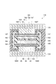
- FIG. 8 is a schematic cross-sectional view showing the semiconductor device 2 according to the second embodiment.
- the semiconductor device 2 has a plurality of submodules 110 arranged between the two coolers 120 and 130.
- the submodule 110 is molded by the resin member 165 and has openings 110B and 110T on the lower surface and the upper surface, respectively.
- the cooler 120 is connected to the intermediate member 90 exposed inside the opening 110 ⁇ / b> B of the submodule 110.
- the cooler 130 is connected to the intermediate member 190 exposed inside the opening 110T of the submodule 110.
- a case 140 is disposed on the side surface of the semiconductor device 2.
- a space surrounded by the coolers 120 and 130 and the case 140 is filled with a resin member 137 so as to seal the submodule 110.
- the heat of the semiconductor element 40 can be radiated from both the upper and lower surfaces. Thereby, heat dissipation performance can be improved.
- FIG. 9 is a partial cross-sectional view schematically showing the semiconductor device 2 according to the second embodiment.
- FIG. 9 is a schematic diagram showing a cross-sectional structure of the submodule 110.
- the submodule 110 includes a semiconductor element 40, an electrode plate 50, and an electrode plate 70. At least one semiconductor element 40 is disposed between the electrode plate 50 and the electrode plate 70.
- the submodule 110 further includes an intermediate member 90 and an intermediate member 190.
- the cooler 120 is electrically connected to the electrode plate 50 via the intermediate member 90.
- the cooler 130 is electrically connected to the electrode plate 70 via the intermediate member 190.
- the semiconductor device 2 includes a positive electrode (not shown) connected to the cooler 120 and a negative electrode (not shown) connected to the cooler 130.
- the intermediate member 190 is, for example, a plate-shaped composite material including a first layer 193, a second layer 195, and a third layer 197.
- the intermediate member 190 is joined to the electrode plate 70 via the joining member 75.
- the cooler 130 is joined to the intermediate member 190 via the joining member 135.
- the joining member 75 and the joining member 135 are, for example, solder materials.
- the bonding member 75 has a melting point higher than that of the bonding member 135.
- the first layer 193 is located between the electrode plate 70 and the second layer 195, and has a linear expansion coefficient that is closer to the linear expansion coefficient of the material of the electrode plate 70 than the linear expansion coefficient of the second layer 195.
- the second layer 195 is located between the cooler 130 and the first layer 193, and has a linear expansion coefficient that is closer to the linear expansion coefficient of the material of the cooler 130 than the linear expansion coefficient of the first layer 193.
- the third layer 197 is located between the cooler 130 and the second layer 195 and has higher wettability with respect to the bonding member 135 than the material of the second layer 195.
- the third layer 197 has a thinner layer thickness than the second layer 195. Further, the third layer 197 is provided so that the layer thickness of the part in contact with the bonding member 135 is thinner than the layer thickness of the peripheral part (see FIG. 5).
- the material of the electrode plates 50 and 70 and the material of the coolers 120 and 130 are different.
- the intermediate members 90 and 190 suppress the thermal deformation (thermal strain) of the bonding members 55, 75, 125, and 135, and improve the reliability of the semiconductor device.
- the material of the electrode plate 50 and the electrode plate 70 is copper or a copper alloy
- the material of the coolers 120 and 130 is aluminum or an aluminum alloy.
- the first layer 93 of the intermediate member 90 and the first layer 193 of the intermediate member 190 are, for example, metal layers mainly composed of copper.
- the second layer 95 of the intermediate member 90 and the second layer 195 of the intermediate member 190 are, for example, metal layers mainly composed of aluminum.
- the third layer 97 of the intermediate member 90 and the third layer 197 of the intermediate member 190 are, for example, metal layers mainly composed of copper.
- the layer thickness of the third layer 97 is thinner than the layer thickness of the first layer 93, and the layer thickness of the third layer 197 is provided thinner than the layer thickness of the first layer 193.
- the resin member 137 is provided so as to cover the joint portion between the intermediate member 90 and the cooler 120 and cover the joint portion between the intermediate member 190 and the cooler 130.
- the resin member 137 does not need to be filled in the entire interior of the semiconductor device 2 and may be disposed so as to cover at least the junction between the intermediate member 90 and the cooler 120 and the junction between the cooler 130 and the intermediate member 190. It ’s fine.
- the intermediate members 90 and 190 alleviate the thermal strain of the joining member between the electrode plate 50 and the cooler 120 and the joining member between the electrode plate 70 and the cooler 130,
- the resin member 137 and the resin member 65 can significantly reduce the thermal strain of the joining member. Thereby, the reliability of the semiconductor device 2 can be improved.
- the submodule 110 includes a case 160 disposed so as to surround the semiconductor element 40, the electrode plates 50 and 70, and the intermediate members 90 and 190.
- Case 160 has openings 160B and 160T on its upper and lower surfaces, respectively.
- the opening 160B is provided so as to be located inside the lower surface of the intermediate member 90 when viewed from below. Further, the opening 160T is provided so as to be located inside the upper surface of the intermediate member 190 when viewed from above. Thereby, the explosive destruction of the submodule 110 due to the failure of the semiconductor element 40 can be avoided.
- coolers 120 and 130 can be used as positive and negative electrodes, it is not necessary to arrange the connection conductor 85 and the bus bar 87 that connect the electrode plates 70 of the submodule 110 to each other, and the configuration can be simplified.
- submodules 10 and 110 may be configured not to include cases 60 and 160.
Landscapes
- Cooling Or The Like Of Semiconductors Or Solid State Devices (AREA)
Abstract
半導体装置は、第1表面と、前記第1表面の裏面側に位置する第2表面と、を有する第1電極板と、前記第1電極板の前記第1表面に対向して配置された第2電極板と、前記第1電極板と前記第2電極板との間に配置され、前記第1電極板および前記第2電極板に接続された少なくとも1つの半導体素子と、前記第1電極板の前記第2表面に対向して配置される第1冷却器と、前記第1電極板と前記第1冷却器の間に配置され、両者に接合される第1中間部材と、を備える。前記第1中間部材は、第1線膨張係数を有する第1層と、第2線膨張係数を有する第2層と、を含む積層構造を有し、前記第1電極板と前記第2層との間に前記第1層が位置するように配置される。前記第1電極板の材料の線膨張係数は、前記第2線膨張係数よりも前記第1線膨張係数に近く、前記第1冷却器の材料の線膨張係数は、前記第1線膨張係数よりも前記第2線膨張係数に近い。
Description
実施形態は、半導体装置に関する。
数キロボルト(kV)の高電圧や、数キロアンペア(kA)の大電流を取り扱う半導体装置では、温度上昇を抑制するために、複数の半導体スイッチング素子を並列接続して動作させる場合がある。例えば、パワー半導体モジュールには、並列接続された複数のスイッチング素子を単一のパッケージに搭載したものがある。
実施形態は、信頼性を向上させた半導体装置を提供する。
実施形態に係る半導体装置は、第1表面と、前記第1表面の裏面側に位置する第2表面と、を有する第1電極板と、前記第1電極板の前記第1表面に対向して配置された第2電極板と、前記第1電極板と前記第2電極板との間に配置され、前記第1電極板および前記第2電極板に接続された少なくとも1つの半導体素子と、前記第1電極板の前記第2表面に対向して配置される第1冷却器と、前記第1電極板と前記第1冷却器の間に配置され、両者に接合される第1中間部材と、を備える。前記第1中間部材は、第1線膨張係数を有する第1層と、第2線膨張係数を有する第2層と、を含む積層構造を有し、前記第1層は、前記第1電極板と前記第2層との間に位置するように配置される。前記第1電極板の材料の線膨張係数は、前記第2線膨張係数よりも前記第1線膨張係数に近く、前記第1冷却器の材料の線膨張係数は、前記第1線膨張係数よりも前記第2線膨張係数に近い。
以下、実施の形態について図面を参照しながら説明する。図面中の同一部分には、同一番号を付してその詳しい説明は適宜省略し、異なる部分について説明する。なお、図面は模式的または概念的なものであり、各部分の厚みと幅との関係、部分間の大きさの比率などは、必ずしも現実のものと同一とは限らない。また、同じ部分を表す場合であっても、図面により互いの寸法や比率が異なって表される場合もある。
さらに、各図中に示すX軸、Y軸およびZ軸を用いて各部分の配置および構成を説明する。X軸、Y軸、Z軸は、相互に直交し、それぞれX方向、Y方向、Z方向を表す。また、Z方向を上方、その反対方向を下方として説明する場合がある。
(第1実施形態)
図1は、第1実施形態に係る半導体装置1を示す模式断面図である。半導体装置1は、例えば、パワー半導体モジュールである。
図1は、第1実施形態に係る半導体装置1を示す模式断面図である。半導体装置1は、例えば、パワー半導体モジュールである。
半導体装置1は、複数のサブモジュール10と、冷却器20と、を備える。サブモジュール10は、例えば、アルミニウムの冷却器20の上に配置される。冷却器20は、サブモジュール10に接続されるマウント部23を有する。
マウント部23は、例えば、上方(Z方向)に突き出た突起であり、サブモジュール10の下面側の開口に挿入される。サブモジュール10の開口とマウント部23との間には、樹脂部材37が配置され、サブモジュール10と冷却器20との間の接続部が封じられる。樹脂部材37は、少なくともサブモジュール10の開口部を充填し、サブモジュール10と冷却器20との間の接合部を保護する。
さらに、冷却器20の上面に配置された複数のサブモジュール10を覆うケース30が配置される。ケース30は、側壁33とカバー35とを含む。側壁33は、複数のサブモジュール10を囲むように設けられ、冷却器20に接続される。カバー35は、複数のサブモジュール10の上面を覆う。ケース30の材料には、例えば、エポキシ樹脂などが用いられる。
図2は、第1実施形態に係る半導体装置1の水平断面を示す模式図である。図2は、サブモジュール10の水平断面を示す模式図であり、図1中に示すA-A線に沿った断面を表している。
図2に示すように、サブモジュール10は、半導体素子40を含む。半導体素子40は、電極板50の上にマウントされ、樹脂部材65により封じられる。電極板50の上には、少なくとも1つの半導体素子40が配置される。この例では、2つの半導体素子40が配置される。
半導体素子40は、例えば、電力変換に用いられるパワー半導体素子である。そのようなパワー半導体素子は、例えば、IGBT(Insulated Gate Bipolar Transistor)、MOSFET(Metal Oxide Semiconductor Field Effect Transistor)等の制御ゲートを有するスイッチング素子、または、FRD(Fast Recovery Diode)等のダイオードである。半導体装置1は、スイッチング素子を含むサブモジュール、および、ダイオード素子を含むサブモジュールの両方を内蔵しても良い。また、1つのサブモジュール内にスイッチング素子とダイオード素子の両方が混在してもよい。
半導体素子40は、例えば、その上面に主電極43と、ゲート電極45と、を有する。主電極43は、例えば、エミッタ電極もしくはソース電極であり、上方に配置される電極板70(図3参照)に接続される。一方、半導体素子40の裏面側に配置されるコレクタ電極もしくはドレイン電極は、電極板50に接続される。さらに、ゲート電極45には、例えば、ゲート端子80がボンディングされる。
サブモジュール10は、例えば、鉄などの金属を含むケース60を含む。ケース60は、後述の樹脂部材65よりも高い剛性を有し、半導体素子40、電極板50および電極板70を囲むように配置される(図3参照)。例えば、サブモジュール10に搭載された半導体素子40のうちの1つに大きな短絡電流が流れるような故障が生じた場合、ケース60は、その周辺に配置された別のサブモジュール10に影響を及ぼすような爆発的故障を防ぐ機能を有していてもよい。
図3は、第1実施形態に係る半導体装置1を模式的に示す部分断面図である。図3は、サブモジュール10の断面構造を示す模式図である。サブモジュール10は、半導体素子40と、電極板50と、電極板70と、ケース60と、を含む。
図3に示すように、例えば、2つの半導体素子40が、電極板50と電極板70との間に配置される。半導体素子40は、例えば、電極板50および電極板70に図示しない接合部材を介して電気的に接続されている。
電極板70は、複数の凸部73を有する。複数の凸部73は、例えば、電極板70に一体に設けられても良いし、電極板70に接合されたものでも良い。凸部73は、図示しない接続部材を介して半導体素子40の主電極43に接続される。
サブモジュール10は、中間部材90をさらに含む。中間部材90は、冷却器20と電極板50との間に配置される。中間部材90は、導電性を有する板状の部材である。また、中間部材90は、複数の金属層を積層した構造を有する複合部材である。
サブモジュール10は、例えば、半導体素子40と、電極板50と、電極板70と、ケース60と、中間部材90と、を樹脂モールドした構造を有する。ケース60は、半導体素子40と、電極板50と、電極板70と、中間部材90と、を囲むように配置され、その下面に開口60Bを有する。開口60Bは、中間部材90の下面よりも狭い開口面積を有する。例えば、開口60Bは、Z方向に見て、中間部材90の外縁よりも内側に位置する。
サブモジュール10は、樹脂部材65によりモールドされる。樹脂部材65は、ケース60の内部に充填され、また、ケース60の外面を覆う。また、サブモジュール10の下面には、開口10Bが設けられる。開口10Bは、ケース60の開口60Bの内側に位置する。開口10Bは、その底面に中間部材90の下面を露出させる。サブモジュール10は、例えば、真空成形を用いて形成される。樹脂部材65は、例えば、熱硬化性樹脂である。
冷却器20のマウント部23は、サブモジュール10の下面の開口10Bに挿入され、接合部材25を介して中間部材90に接合される。電極板50は、接合部材55を介して中間部材90に接合される。これにより、冷却器20と電極板50とが電気的に接続される。接合部材25および接合部材55は、例えば、ハンダ材である。接合部材25は、例えば、接合部材55の融点よりも低い融点を有する。これにより、接合部材55を溶融させることなく、サブモジュール10を冷却器20の上にマウントすることができるので、半導体装置1の組み立てが容易になる。
半導体素子40において発生するジュール熱は、電極板50、中間部材90および冷却器20を介して外部に放散される。冷却器20は、複数の空洞20Sを有する。例えば、空洞20Sに冷却液を循環させることにより、半導体素子40において発生するジュール熱を効果的に放散させることができる。
冷却器20のマウント部23が挿入された開口10Bには、樹脂部材37が充填される。冷却器20と中間部材90との間の接続部は、樹脂部材37により封止られる。また、電極板50と中間部材90との間の接続部も樹脂部材65により封じられる。
図4は、第1実施形態に係る半導体装置1の構成を模式的に示す斜視図である。図4に示すように、複数のサブモジュール10が冷却器20の上面に配置される。なお、図4では、複数のサブモジュール10を囲むケース30およびその内部に配置される樹脂の表示を省略している。
サブモジュール10において、ケース60は、ゲート端子80の延在方向の側面にも開口を有する。そして、ゲート端子80は、ケース60の内部に充填された図示しない樹脂部材65から延出するように設けられる。また、電極板70に接続された電極端子83も、ゲート端子80と同じ方向に延出するように設けられる。
各サブモジュール10の電極端子83は、接続導体85を介してバスバー87に接続される。これにより、電極板50と電極板70との間に配置された複数の半導体素子40を、冷却器20とバスバー87との間に並列接続できる。
例えば、半導体装置1の図示しない正極は、冷却器20および電極板50を介して半導体素子40に電気的に接続される。一方、半導体装置1の図示しない負極は、バスバー87および電極板70を介して半導体素子40に電気的に接続される。
このような半導体装置1において、電極板50、電極板70およびゲート端子80の材料は、例えば、電気伝導性および熱伝導性が高い銅またはアルミニウムを主成分として含む金属材料である。また、冷却器20の材料も銅またはアルミニウムを主成分として含む金属材料である。
本実施形態に係る半導体装置1では、冷却器20と電極板50との間に中間部材90を配置することにより、その信頼性を向上させることができる。例えば、図10に示す比較例に係るサブモジュール10Xでは、冷却器20と電極板50との間に中間部材90が配置されず、冷却器20と電極板50とが接合部材25を介して接合されている。
例えば、体積比率の大きい冷却器20には、軽量化を図るために、比重の軽いアルミニウムを用いることが好ましい。一方、電極板50および70には、電気抵抗率が小さく、熱伝導率が大きい銅を用いることが好ましい。結果として、冷却器20の材料と電極板50の材料とが異なる場合がある。
高電圧および大電流を制御する半導体装置1では、冷却器20を用いたとしても、サブモジュール10の温度上昇を完全に抑制することは難しい。このため、冷却器20の熱膨張と電極板50の熱膨張の違いに起因する歪が、接合部材25に加わる。
図10中の矢印で示すように、アルミニウムを材料とする冷却器20の熱膨張は、銅を材料とする電極板50の熱膨張よりも大きい。そして、この違いに起因する熱歪により、接合部材25が劣化し、半導体装置1の信頼性に影響を与えることがある。これに対し、半導体装置1では、中間部材90を配置することにより、接合部材25および接合部材55に加わる熱歪を緩和することが可能となる。これにより、半導体装置1の信頼性を向上させることができる。
図5は、第1実施形態に係る半導体装置1の接続構造を示す模式断面図である。図5は、冷却器20と中間部材90との間、および、電極板50と中間部材90との間の接続構造を表した模式図である。
中間部材90は、少なくとも2つの異なる金属層を含む板状部材である。中間部材90は、例えば、第1層93および第2層95を含む。第1層93は、電極板50と第2層95との間に位置し、第1層厚T1を有する。第1層93は、第2層95の線膨張係数よりも電極板50の材料の線膨張係数に近い値の線膨張係数を有する。
第2層95は、冷却器20のマウント部23と第1層93との間に位置し、第2層厚T2を有する。第2層95は、第1層93の線膨張係数よりも冷却器20の材料の線膨張係数に近い値の線膨張係数を有する。
例えば、第1層93は、電極板50と同じ材料を含む。また、第2層95は、冷却器20と同じ材料を含む。第1層93は、例えば、銅を含む金属層であり、第2層95は、例えば、アルミニウムを含む金属層である。
中間部材90は、例えば、冷却器20と第2層95との間に位置する第3層97をさらに含むことができる。例えば、冷却器20と中間部材90とを接合する接合部材25に対する第2層95の濡れ性が低い場合、接合部材25に対する濡れ性の高い第3層97を配置することが好ましい。第3層97は、例えば、銅を含む金属層である。
例えば、サブモジュール10を冷却器20の上にマウントする場合、接合部材25に対する濡れ性を向上させるために、サブモジュール10の下面側の開口10B(図3参照)に露出された中間部材90の表層を、例えば、機械的加工により除去することが好ましい。これにより、サブモジュール10の形成過程において中間部材90の露出面に生じる酸化膜もしくは汚れなどを除去し、中間部材90の接合部材25に対する濡れ性を向上させることができる。結果として、第3層97の接合部材25に接する部分の第3層厚T3は、樹脂部材65に覆われる周辺部の第4層厚T4よりも薄くなる。
また、第3層97に代えて、中間部材90の露出面に、接合部材25に対する濡れ性の高い材料、例えば、ニッケルもしくは銅などのメッキ層を形成しても良い。さらに、冷却器20のマウント部23の表面にも、接合部材25に対する濡れ性の高い材料をメッキすることが好ましい。これにより、サブモジュール10と冷却器20との間の接合強度を向上させることができる。
図6は、第1実施形態に係る半導体装置1の特性を示す模式断面図である。図6は、冷却器20と電極板50との間に配置された中間部材90の作用を例示する模式図である。図6中に示す矢印は、各部材の熱膨張を模式的に表している。
図6に示すように、中間部材90の第1層93は、電極板50の熱膨張と略同一の熱膨張を有する。このため、電極板50と第1層93との間に位置する接合部材55に加わる熱歪を緩和することができる。また、第1層93は、第2層95の熱膨張が接合部材55に与える影響を抑制できる第1層厚T1(図5参照)を有する。
中間部材90の第2層95は、冷却器20の熱膨張と略同一の熱膨張を有する。このため、冷却器20と第2層95との間に位置する接合部材25に加わる熱歪を緩和することができる。第2層95は、第1層93の熱膨張が接合部材25に与える影響を抑制できる第2層厚T2を有する。
第3層97は、第2層による接合部材25の歪緩和の効果を妨げない第3層厚T3を有する。例えば、第3層厚T3は、第2層厚T2よりも薄い(図5参照)。さらに、第1層93と第3層97に同じ材料、例えば、銅を用いた場合、第1層厚T1は、第3層厚T3よりも厚い。
また、樹脂部材37と樹脂部材65は、異なる線膨張係数を有する。例えば、冷却器20と中間部材90との間に位置する接合部材25の端部を覆う樹脂部材37には、冷却器20の材料の線膨張係数に近い値の線膨張係数を有する材料を用いる。一方、電極板50と中間部材90との間に位置する接合部材55の端部を覆う樹脂部材65には、電極板50の材料の線膨張係数に近い値の線膨張係数を有する材料を用いる。
例えば、樹脂部材37には、銅の線膨張係数よりもアルミニウムの線膨張係数に近い値の線膨張係数を有する材料を用いる。樹脂部材65には、例えば、アルミニウムの線膨張係数よりも銅の線膨張係数に近い値の線膨張係数を有する材料を用いる。樹脂部材37および樹脂部材65は、例えば、エポキシ樹脂であり、樹脂部材37は、樹脂部材65とは異なる組成のエポキシ樹脂である。
半導体装置1では、動作時の温度変化によってサブモジュール10が熱膨張もしくは熱収縮した際に、冷却器20の材料と電極板50の材料との間の線膨張係数の差に起因する接合部材25および55の歪(熱変形)を、中間部材90が緩和する。
さらに、樹脂部材37により冷却器20と中間部材90との間に位置する接合部材25を封止し、樹脂部材65により電極板50と中間部材90との間の接合部材55を封止することにより、接合部材25および55の熱変形を効果的に抑制することができる。例えば、樹脂部材37の線膨張係数を冷却器20の材料の線膨張係数に近い値とし、樹脂部材65の線膨張係数を電極板50の材料の線膨張係数に近い値とすることにより、接合部材25および55の歪を大幅に抑制することができる。
図7は、第1実施形態に係る半導体装置1の特性を示すグラフである。図7は、接合部材の歪と、半導体装置1の寿命と、の関係を示すグラフである。横軸は、接合部材の歪の大きさであり、縦軸は、温度上昇および低下のサイクル数で表される装置寿命である。
図7に示すように、冷却器20と電極板50とを直接接合した場合に比べて、中間部材を介在させることにより、熱歪を低減し、装置寿命を延ばすことができる。また、接合部を樹脂部材で封じることにより、さらに熱歪を低減し、装置寿命を延ばすことができる。
このように、冷却器20と電極板50との間に中間部材90を介在させることによる歪の低減効果、および、各接合部を樹脂部材37および65で封止することによる歪の低減効果により、図10に示すサブモジュール10Xを用いる場合と比べて、半導体装置1の寿命を大幅に延ばすことができる。
さらに、中間部材90の下面をケース60の開口60Bよりも広くすることにより、サブモジュール10の防爆効果を向上させることができる。例えば、何らかの要因により半導体素子40が故障し、大きな短絡電流が流れると、例えば、接合部材の気化により、半導体素子40を封じた樹脂部材65の内圧が上昇する。このため、電極板50と電極板70を互いに離間させる方向に荷重が生じるが、ケース60は、その荷重に耐え、電極板50と電極板70の離間を防ぐ。その結果、サブモジュール10の破裂(爆発的故障)を抑制することが可能となり、半導体素子40のいずれかが故障したとしても半導体装置1への通電を継続することができる。例えば、半導体装置1を多段化して構成される電力変換器の運転継続を実現することができる。
(第2実施形態)
図8は、第2実施形態に係る半導体装置2を示す模式断面図である。半導体装置2は、2つの冷却器120および130の間に配置された複数のサブモジュール110を有する。
図8は、第2実施形態に係る半導体装置2を示す模式断面図である。半導体装置2は、2つの冷却器120および130の間に配置された複数のサブモジュール110を有する。
サブモジュール110は、樹脂部材165によりモールドされ、下面および上面にそれぞれ開口110Bおよび110Tを有する。冷却器120は、サブモジュール110の開口110Bの内部に露出された中間部材90に接続される。冷却器130は、サブモジュール110の開口110Tの内部に露出された中間部材190に接続される。
半導体装置2の側面には、ケース140が配置される。冷却器120、130およびケース140に囲まれた空間には、樹脂部材137がサブモジュール110を封止するように充填される。
半導体装置2では、上下に2つの冷却器120および130を配置することにより、半導体素子40の熱を、上下両面から放熱することができる。これにより、放熱性能を向上させることができる。
図9は、第2実施形態に係る半導体装置2を模式的に示す部分断面図である。図9は、サブモジュール110の断面構造を示す模式図である。サブモジュール110は、半導体素子40と、電極板50と、電極板70と、を含む。少なくとも1つの半導体素子40が、電極板50と電極板70との間に配置される。
サブモジュール110は、中間部材90と、中間部材190と、をさらに含む。冷却器120は、中間部材90を介して電極板50に電気的に接続される。冷却器130は、中間部材190を介して電極板70に電気的に接続される。半導体装置2は、例えば、冷却器120に接続された図示しない正極と、冷却器130に接続された図示しない負極と、を有する。
中間部材190は、例えば、第1層193と、第2層195と、第3層197と、を含む板状複合材である。中間部材190は、接合部材75を介して電極板70に接合される。また、冷却器130は、接合部材135を介して中間部材190に接合される。接合部材75および接合部材135は、例えば、ハンダ材である。接合部材75は、例えば、接合部材135の融点よりも高い融点を有する。
第1層193は、電極板70と第2層195との間に位置し、第2層195の線膨張係数よりも電極板70の材料の線膨張係数に近い値の線膨張係数を有する。
第2層195は、冷却器130と第1層193との間に位置し、第1層193の線膨張係数よりも冷却器130の材料の線膨張係数に近い値の線膨張係数を有する。
第3層197は、冷却器130と第2層195との間に位置し、第2層195の材料よりも接合部材135に対する濡れ性が高い。第3層197は、第2層195よりも薄い層厚を有する。また、第3層197は、接合部材135に接する部分の層厚が、周辺部の層厚よりも薄くなるように設けられる(図5参照)。
本実施形態でも、電極板50および70の材料と、冷却器120および130の材料とが異なる。中間部材90および190は、接合部材55、75、125、135の熱変形(熱歪)を抑制し、半導体装置の信頼性を向上させる。
例えば、電極板50および電極板70の材料は、銅もしくは銅合金であり、冷却器120および130の材料は、アルミニウムもしくはアルミニウム合金である。
中間部材90の第1層93および中間部材190の第1層193は、例えば、銅を主成分とする金属層である。中間部材90の第2層95および中間部材190の第2層195は、例えば、アルミニウムを主成分とする金属層である。
さらに、中間部材90の第3層97および中間部材190の第3層197は、例えば、銅を主成分とする金属層である。第3層97の層厚は、第1層93の層厚よりも薄く、第3層197の層厚は、第1層193の層厚よりも薄く設けられる。
樹脂部材137は、中間部材90と冷却器120の接合部を覆い、中間部材190と冷却器130の接合部を覆うように設けられる。樹脂部材137は、半導体装置2の内部全体に充填される必要はなく、少なくとも中間部材90と冷却器120の接合部、冷却器130と中間部材190との接合部を覆うように配置されていれば良い。
本実施例においても、電極板50と冷却器120との間の接合部材、および、電極板70と冷却器130との間の接合部材の熱歪を、中間部材90および190で緩和すると共に、樹脂部材137および樹脂部材65により接合部材の熱歪を大幅に低減することができる。これにより、半導体装置2の信頼性を向上させることができる。
また、サブモジュール110は、半導体素子40、電極板50、70、中間部材90および190を囲むように配置されるケース160を含む。ケース160は、上面および下面にそれぞれ開口160Bおよび160Tを有する。
開口160Bは、下方から見て中間部材90の下面の内側に位置するように設けられる。また、開口160Tは、上方から見て、中間部材190の上面の内側に位置するように設けられる。これにより、半導体素子40の故障によるサブモジュール110の爆発的破壊を回避することができる。
さらに、冷却器120および130を正負の電極として用いることができるため、サブモジュール110の電極板70を相互に接続する接続導体85およびやバスバー87を配置する必要がなく、構成を簡略化できる。
上記の半導体装置1および2は例示であり、実施形態は、これらに限定される訳ではない。例えば、半導体装置1および2に比べて低電圧および低電流の用途に用いられる装置では、サブモジュール10および110は、ケース60および160を含まない構成であっても良い。
本発明のいくつかの実施形態を説明したが、これらの実施形態は、例として提示したものであり、発明の範囲を限定することは意図していない。これら新規な実施形態は、その他の様々な形態で実施されることが可能であり、発明の要旨を逸脱しない範囲で、種々の省略、置き換え、変更を行うことができる。これら実施形態やその変形は、発明の範囲や要旨に含まれるとともに、請求の範囲に記載された発明とその均等の範囲に含まれる。
Claims (10)
- 第1表面と、前記第1表面の裏面側に位置する第2表面と、を有する第1電極板と、
前記第1電極板の前記第1表面に対向して配置された第2電極板と、
前記第1電極板と前記第2電極板との間に配置され、前記第1電極板および前記第2電極板に接続された少なくとも1つの半導体素子と、
前記第1電極板の前記第2表面に対向して配置される第1冷却器と、
前記第1電極板と前記第1冷却器の間に配置され、両者に接合される第1中間部材と、
を備え、
前記第1中間部材は、第1線膨張係数を有する第1層と、第2線膨張係数を有する第2層と、を含む積層構造を有し、前記第1電極板と前記第2層との間に前記第1層が位置するように配置され、
前記第1電極板の材料の線膨張係数は、前記第2線膨張係数よりも前記第1線膨張係数に近く、
前記第1冷却器の材料の線膨張係数は、前記第1線膨張係数よりも前記第2線膨張係数に近い半導体装置。 - 前記第1電極板と前記第1中間部材との間に配置された第1接合部材と、
前記第1冷却器と前記第1中間部材との間に配置された第2接合部材と、
をさらに備えた請求項1記載の半導体装置。 - 前記第1接合部材の融点は、前記第2接合部材の融点よりも高い請求項2記載の半導体装置。
- 前記中間部材は、前記第2接合部材に対するぬれ性が前記第2層よりも高い第3層をさらに含み、
前記第3層は、前記第2層と前記第2接合部材との間に配置され、前記第2接合部材と接する部分において前記第2層よりも薄い層厚を有する請求項2記載の半導体装置。 - 前記第1接合部材の端および前記第2接合部材の端を覆う樹脂部材をさらに備えた請求項2記載の半導体装置。
- 前記樹脂部材は、前記第1接合部材の端を覆う第1樹脂部材と、前記第2接合部材の端を覆う第2樹脂部材と、を含み、
前記第1樹脂部材の線膨張係数は、前記第2樹脂部材の線膨張係数とは異なる値を有する請求項5記載の半導体装置。 - 前記第2電極板、前記半導体素子、前記第1電極板および前記中間部材を囲む第1ケースと、
前記第1ケースの外側に配置された第2ケースと、
をさらに備え、
前記第1ケースは、前記第1樹脂部材よりも剛性が高く、
前記第1ケースは、前記中間部材の一部を露出させる開口を有し、
前記第1冷却器は、前記第1ケースの開口内に延在し、前記中間部材の前記一部に接合される部分を有する請求項6記載の半導体装置。 - 前記中間部材の前記第1層は、前記第1電極板と同じ材料を含み、
前記中間部材の前記第2層は、前記第1冷却器と同じ材料を含む請求項1記載の半導体装置。 - 前記第1層は、銅を含む金属層であり、
前記第2層は、アルミニウムを含む金属層である請求項8記載の半導体装置。 - 前記第2電極板に対向して配置された第2冷却器と、
前記第2電極板と前記第2冷却器との間に配置された第2中間部材と、
をさらに備え、
前記第2電極板は、前記第1電極板と前記第2冷却器との間に位置し、
前記第2中間部材は、第3線膨張係数を有する第3層と、第4線膨張係数を有する第4層と、を含む積層構造を有し、前記第2電極板と前記第4層との間に前記第3層が位置するように配置され、
前記第2電極板の材料の線膨張係数は、前記第4線膨張係数よりも前記第3線膨張係数に近く、
前記第2冷却器の材料の線膨張係数は、前記第3線膨張係数よりも前記第4線膨張係数に近い請求項1記載の半導体装置。
Applications Claiming Priority (2)
| Application Number | Priority Date | Filing Date | Title |
|---|---|---|---|
| JP2018044505A JP2021082617A (ja) | 2018-03-12 | 2018-03-12 | 半導体装置 |
| JP2018-044505 | 2018-03-12 |
Publications (1)
| Publication Number | Publication Date |
|---|---|
| WO2019176129A1 true WO2019176129A1 (ja) | 2019-09-19 |
Family
ID=67907022
Family Applications (1)
| Application Number | Title | Priority Date | Filing Date |
|---|---|---|---|
| PCT/JP2018/029629 Ceased WO2019176129A1 (ja) | 2018-03-12 | 2018-08-07 | 半導体装置 |
Country Status (2)
| Country | Link |
|---|---|
| JP (1) | JP2021082617A (ja) |
| WO (1) | WO2019176129A1 (ja) |
Citations (6)
| Publication number | Priority date | Publication date | Assignee | Title |
|---|---|---|---|---|
| WO2011093373A1 (ja) * | 2010-01-27 | 2011-08-04 | 京セラ株式会社 | 複合体およびそれを用いた半導体装置、半導体モジュールならびにその製法 |
| JP2013038309A (ja) * | 2011-08-10 | 2013-02-21 | Denso Corp | 半導体モジュールおよびそれを備えた半導体装置 |
| WO2013111276A1 (ja) * | 2012-01-25 | 2013-08-01 | 三菱電機株式会社 | 電力用半導体装置 |
| WO2014064806A1 (ja) * | 2012-10-25 | 2014-05-01 | 三菱電機株式会社 | 半導体装置 |
| WO2015029511A1 (ja) * | 2013-08-28 | 2015-03-05 | 三菱電機株式会社 | 半導体装置およびその製造方法 |
| WO2016121159A1 (ja) * | 2015-01-26 | 2016-08-04 | 三菱電機株式会社 | 半導体装置および半導体装置の製造方法 |
-
2018
- 2018-03-12 JP JP2018044505A patent/JP2021082617A/ja active Pending
- 2018-08-07 WO PCT/JP2018/029629 patent/WO2019176129A1/ja not_active Ceased
Patent Citations (6)
| Publication number | Priority date | Publication date | Assignee | Title |
|---|---|---|---|---|
| WO2011093373A1 (ja) * | 2010-01-27 | 2011-08-04 | 京セラ株式会社 | 複合体およびそれを用いた半導体装置、半導体モジュールならびにその製法 |
| JP2013038309A (ja) * | 2011-08-10 | 2013-02-21 | Denso Corp | 半導体モジュールおよびそれを備えた半導体装置 |
| WO2013111276A1 (ja) * | 2012-01-25 | 2013-08-01 | 三菱電機株式会社 | 電力用半導体装置 |
| WO2014064806A1 (ja) * | 2012-10-25 | 2014-05-01 | 三菱電機株式会社 | 半導体装置 |
| WO2015029511A1 (ja) * | 2013-08-28 | 2015-03-05 | 三菱電機株式会社 | 半導体装置およびその製造方法 |
| WO2016121159A1 (ja) * | 2015-01-26 | 2016-08-04 | 三菱電機株式会社 | 半導体装置および半導体装置の製造方法 |
Also Published As
| Publication number | Publication date |
|---|---|
| JP2021082617A (ja) | 2021-05-27 |
Similar Documents
| Publication | Publication Date | Title |
|---|---|---|
| JP6065995B2 (ja) | 半導体装置及び半導体装置の製造方法 | |
| CN105027412B (zh) | 电力变换装置 | |
| JP6591556B2 (ja) | 電力変換装置 | |
| JP6422592B2 (ja) | 電力変換装置 | |
| JP6286543B2 (ja) | パワーモジュール装置、電力変換装置およびパワーモジュール装置の製造方法 | |
| JP7172847B2 (ja) | 半導体装置 | |
| CN111668165A (zh) | 半导体模块和具备该半导体模块的半导体装置 | |
| US11735557B2 (en) | Power module of double-faced cooling | |
| JP2023085765A (ja) | 半導体装置及び半導体装置の製造方法 | |
| JP6860453B2 (ja) | パワー半導体モジュール | |
| JP6286541B2 (ja) | パワーモジュール装置及び電力変換装置 | |
| JP2018081980A (ja) | 半導体装置 | |
| WO2013118275A1 (ja) | 半導体装置 | |
| WO2017130370A1 (ja) | 半導体装置 | |
| WO2018151010A1 (ja) | 半導体装置 | |
| JP7290420B2 (ja) | パワー半導体装置 | |
| WO2019176129A1 (ja) | 半導体装置 | |
| KR20180087330A (ko) | 파워 모듈의 양면 냉각을 위한 금속 슬러그 | |
| JP6730450B2 (ja) | 半導体装置 | |
| US20240030085A1 (en) | Semiconductor module and method of manufacturing the same | |
| JP2019021831A (ja) | 半導体装置及び半導体装置用サブモジュール | |
| JP6922002B2 (ja) | 半導体装置 | |
| JP2022050058A (ja) | 半導体装置及び半導体装置の製造方法 | |
| JP6953859B2 (ja) | 半導体装置 | |
| JP7643497B1 (ja) | 電力変換装置 |
Legal Events
| Date | Code | Title | Description |
|---|---|---|---|
| 121 | Ep: the epo has been informed by wipo that ep was designated in this application |
Ref document number: 18909897 Country of ref document: EP Kind code of ref document: A1 |
|
| NENP | Non-entry into the national phase |
Ref country code: DE |
|
| 122 | Ep: pct application non-entry in european phase |
Ref document number: 18909897 Country of ref document: EP Kind code of ref document: A1 |
|
| NENP | Non-entry into the national phase |
Ref country code: JP |