WO2019168365A1 - 중합체, 이를 포함하는 코팅 조성물 및 이를 이용한 유기 발광 소자 - Google Patents
중합체, 이를 포함하는 코팅 조성물 및 이를 이용한 유기 발광 소자 Download PDFInfo
- Publication number
- WO2019168365A1 WO2019168365A1 PCT/KR2019/002410 KR2019002410W WO2019168365A1 WO 2019168365 A1 WO2019168365 A1 WO 2019168365A1 KR 2019002410 W KR2019002410 W KR 2019002410W WO 2019168365 A1 WO2019168365 A1 WO 2019168365A1
- Authority
- WO
- WIPO (PCT)
- Prior art keywords
- group
- substituted
- unsubstituted
- present specification
- polymer
- Prior art date
Links
- 229920000642 polymer Polymers 0.000 title claims abstract description 75
- 239000008199 coating composition Substances 0.000 title claims abstract description 57
- 239000000126 substance Substances 0.000 claims abstract description 26
- 239000000463 material Substances 0.000 claims description 68
- 239000011368 organic material Substances 0.000 claims description 57
- 238000002347 injection Methods 0.000 claims description 46
- 239000007924 injection Substances 0.000 claims description 46
- 238000000034 method Methods 0.000 claims description 36
- 125000004432 carbon atom Chemical group C* 0.000 claims description 32
- 125000003118 aryl group Chemical group 0.000 claims description 31
- 125000000217 alkyl group Chemical group 0.000 claims description 22
- 230000005525 hole transport Effects 0.000 claims description 21
- 125000001424 substituent group Chemical group 0.000 claims description 20
- 125000000732 arylene group Chemical group 0.000 claims description 17
- 125000003277 amino group Chemical group 0.000 claims description 14
- UFHFLCQGNIYNRP-UHFFFAOYSA-N Hydrogen Chemical compound [H][H] UFHFLCQGNIYNRP-UHFFFAOYSA-N 0.000 claims description 12
- 125000002947 alkylene group Chemical group 0.000 claims description 12
- 125000000623 heterocyclic group Chemical group 0.000 claims description 12
- 229910052739 hydrogen Inorganic materials 0.000 claims description 12
- 239000001257 hydrogen Substances 0.000 claims description 12
- 125000003983 fluorenyl group Chemical group C1(=CC=CC=2C3=CC=CC=C3CC12)* 0.000 claims description 11
- 125000001997 phenyl group Chemical group [H]C1=C([H])C([H])=C(*)C([H])=C1[H] 0.000 claims description 10
- 125000003545 alkoxy group Chemical group 0.000 claims description 9
- 238000010438 heat treatment Methods 0.000 claims description 9
- 125000004104 aryloxy group Chemical group 0.000 claims description 7
- 125000000753 cycloalkyl group Chemical group 0.000 claims description 7
- 125000005843 halogen group Chemical group 0.000 claims description 7
- 125000005549 heteroarylene group Chemical group 0.000 claims description 7
- 125000006267 biphenyl group Chemical group 0.000 claims description 6
- 125000001624 naphthyl group Chemical group 0.000 claims description 6
- 125000002560 nitrile group Chemical group 0.000 claims description 5
- YJTKZCDBKVTVBY-UHFFFAOYSA-N 1,3-Diphenylbenzene Chemical group C1=CC=CC=C1C1=CC=CC(C=2C=CC=CC=2)=C1 YJTKZCDBKVTVBY-UHFFFAOYSA-N 0.000 claims description 4
- UFHFLCQGNIYNRP-VVKOMZTBSA-N Dideuterium Chemical compound [2H][2H] UFHFLCQGNIYNRP-VVKOMZTBSA-N 0.000 claims description 4
- 125000002887 hydroxy group Chemical group [H]O* 0.000 claims description 3
- 125000005561 phenanthryl group Chemical group 0.000 claims description 3
- 239000010410 layer Substances 0.000 description 134
- -1 4-vinylphenyl Chemical group 0.000 description 67
- 150000001875 compounds Chemical class 0.000 description 55
- YXFVVABEGXRONW-UHFFFAOYSA-N Toluene Chemical compound CC1=CC=CC=C1 YXFVVABEGXRONW-UHFFFAOYSA-N 0.000 description 46
- XEKOWRVHYACXOJ-UHFFFAOYSA-N Ethyl acetate Chemical compound CCOC(C)=O XEKOWRVHYACXOJ-UHFFFAOYSA-N 0.000 description 36
- 239000002904 solvent Substances 0.000 description 28
- 238000002360 preparation method Methods 0.000 description 27
- WYURNTSHIVDZCO-UHFFFAOYSA-N Tetrahydrofuran Chemical compound C1CCOC1 WYURNTSHIVDZCO-UHFFFAOYSA-N 0.000 description 26
- VLKZOEOYAKHREP-UHFFFAOYSA-N n-Hexane Chemical compound CCCCCC VLKZOEOYAKHREP-UHFFFAOYSA-N 0.000 description 21
- 239000000243 solution Substances 0.000 description 20
- XLYOFNOQVPJJNP-UHFFFAOYSA-N water Chemical compound O XLYOFNOQVPJJNP-UHFFFAOYSA-N 0.000 description 20
- 125000000843 phenylene group Chemical group C1(=C(C=CC=C1)*)* 0.000 description 16
- YMWUJEATGCHHMB-UHFFFAOYSA-N Dichloromethane Chemical compound ClCCl YMWUJEATGCHHMB-UHFFFAOYSA-N 0.000 description 15
- LFQSCWFLJHTTHZ-UHFFFAOYSA-N Ethanol Chemical compound CCO LFQSCWFLJHTTHZ-UHFFFAOYSA-N 0.000 description 15
- 230000032258 transport Effects 0.000 description 15
- YLQBMQCUIZJEEH-UHFFFAOYSA-N Furan Chemical group C=1C=COC=1 YLQBMQCUIZJEEH-UHFFFAOYSA-N 0.000 description 14
- 239000002019 doping agent Substances 0.000 description 14
- 239000012044 organic layer Substances 0.000 description 14
- 239000000758 substrate Substances 0.000 description 14
- 238000006243 chemical reaction Methods 0.000 description 13
- OZAIFHULBGXAKX-UHFFFAOYSA-N 2-(2-cyanopropan-2-yldiazenyl)-2-methylpropanenitrile Chemical compound N#CC(C)(C)N=NC(C)(C)C#N OZAIFHULBGXAKX-UHFFFAOYSA-N 0.000 description 10
- 230000008569 process Effects 0.000 description 10
- 229910052751 metal Inorganic materials 0.000 description 9
- 239000002184 metal Substances 0.000 description 9
- CSCPPACGZOOCGX-UHFFFAOYSA-N Acetone Chemical compound CC(C)=O CSCPPACGZOOCGX-UHFFFAOYSA-N 0.000 description 8
- 229910052782 aluminium Inorganic materials 0.000 description 8
- XAGFODPZIPBFFR-UHFFFAOYSA-N aluminium Chemical compound [Al] XAGFODPZIPBFFR-UHFFFAOYSA-N 0.000 description 8
- 239000012153 distilled water Substances 0.000 description 8
- 235000019441 ethanol Nutrition 0.000 description 8
- 238000004519 manufacturing process Methods 0.000 description 7
- 150000004982 aromatic amines Chemical class 0.000 description 6
- 230000015572 biosynthetic process Effects 0.000 description 6
- 229910052799 carbon Inorganic materials 0.000 description 6
- 230000000052 comparative effect Effects 0.000 description 6
- 238000000151 deposition Methods 0.000 description 6
- DMBHHRLKUKUOEG-UHFFFAOYSA-N diphenylamine Chemical compound C=1C=CC=CC=1NC1=CC=CC=C1 DMBHHRLKUKUOEG-UHFFFAOYSA-N 0.000 description 6
- RAXXELZNTBOGNW-UHFFFAOYSA-N imidazole Natural products C1=CNC=N1 RAXXELZNTBOGNW-UHFFFAOYSA-N 0.000 description 6
- PQXKHYXIUOZZFA-UHFFFAOYSA-M lithium fluoride Chemical compound [Li+].[F-] PQXKHYXIUOZZFA-UHFFFAOYSA-M 0.000 description 6
- 125000002496 methyl group Chemical group [H]C([H])([H])* 0.000 description 6
- 229910052757 nitrogen Inorganic materials 0.000 description 6
- BWHMMNNQKKPAPP-UHFFFAOYSA-L potassium carbonate Chemical compound [K+].[K+].[O-]C([O-])=O BWHMMNNQKKPAPP-UHFFFAOYSA-L 0.000 description 6
- 125000000999 tert-butyl group Chemical group [H]C([H])([H])C(*)(C([H])([H])[H])C([H])([H])[H] 0.000 description 6
- OKTJSMMVPCPJKN-UHFFFAOYSA-N Carbon Chemical compound [C] OKTJSMMVPCPJKN-UHFFFAOYSA-N 0.000 description 5
- ZMXDDKWLCZADIW-UHFFFAOYSA-N N,N-Dimethylformamide Chemical compound CN(C)C=O ZMXDDKWLCZADIW-UHFFFAOYSA-N 0.000 description 5
- 125000002529 biphenylenyl group Chemical group C1(=CC=CC=2C3=CC=CC=C3C12)* 0.000 description 5
- 239000010406 cathode material Substances 0.000 description 5
- 230000000694 effects Effects 0.000 description 5
- 125000001072 heteroaryl group Chemical group 0.000 description 5
- 238000004770 highest occupied molecular orbital Methods 0.000 description 5
- 125000001570 methylene group Chemical group [H]C([H])([*:1])[*:2] 0.000 description 5
- 239000000178 monomer Substances 0.000 description 5
- UOXJNGFFPMOZDM-UHFFFAOYSA-N 2-[di(propan-2-yl)amino]ethylsulfanyl-methylphosphinic acid Chemical compound CC(C)N(C(C)C)CCSP(C)(O)=O UOXJNGFFPMOZDM-UHFFFAOYSA-N 0.000 description 4
- CDBYLPFSWZWCQE-UHFFFAOYSA-L Sodium Carbonate Chemical compound [Na+].[Na+].[O-]C([O-])=O CDBYLPFSWZWCQE-UHFFFAOYSA-L 0.000 description 4
- XLOMVQKBTHCTTD-UHFFFAOYSA-N Zinc monoxide Chemical compound [Zn]=O XLOMVQKBTHCTTD-UHFFFAOYSA-N 0.000 description 4
- 239000010405 anode material Substances 0.000 description 4
- RWCCWEUUXYIKHB-UHFFFAOYSA-N benzophenone Chemical compound C=1C=CC=CC=1C(=O)C1=CC=CC=C1 RWCCWEUUXYIKHB-UHFFFAOYSA-N 0.000 description 4
- 150000001616 biphenylenes Chemical group 0.000 description 4
- DBDNZCBRIPTLJF-UHFFFAOYSA-N boron(1-) monohydride Chemical compound [BH-] DBDNZCBRIPTLJF-UHFFFAOYSA-N 0.000 description 4
- 238000004440 column chromatography Methods 0.000 description 4
- 239000013256 coordination polymer Substances 0.000 description 4
- 125000005567 fluorenylene group Chemical group 0.000 description 4
- 125000001449 isopropyl group Chemical group [H]C([H])([H])C([H])(*)C([H])([H])[H] 0.000 description 4
- 239000011572 manganese Substances 0.000 description 4
- 150000002739 metals Chemical class 0.000 description 4
- 125000004957 naphthylene group Chemical group 0.000 description 4
- 229910052760 oxygen Inorganic materials 0.000 description 4
- 238000007639 printing Methods 0.000 description 4
- MFRIHAYPQRLWNB-UHFFFAOYSA-N sodium tert-butoxide Chemical compound [Na+].CC(C)(C)[O-] MFRIHAYPQRLWNB-UHFFFAOYSA-N 0.000 description 4
- ZWEHNKRNPOVVGH-UHFFFAOYSA-N 2-Butanone Chemical compound CCC(C)=O ZWEHNKRNPOVVGH-UHFFFAOYSA-N 0.000 description 3
- GMHHTGYHERDNLO-UHFFFAOYSA-N 4-bromobicyclo[4.2.0]octa-1(6),2,4-triene Chemical compound BrC1=CC=C2CCC2=C1 GMHHTGYHERDNLO-UHFFFAOYSA-N 0.000 description 3
- SFHYNDMGZXWXBU-LIMNOBDPSA-N 6-amino-2-[[(e)-(3-formylphenyl)methylideneamino]carbamoylamino]-1,3-dioxobenzo[de]isoquinoline-5,8-disulfonic acid Chemical compound O=C1C(C2=3)=CC(S(O)(=O)=O)=CC=3C(N)=C(S(O)(=O)=O)C=C2C(=O)N1NC(=O)N\N=C\C1=CC=CC(C=O)=C1 SFHYNDMGZXWXBU-LIMNOBDPSA-N 0.000 description 3
- IJGRMHOSHXDMSA-UHFFFAOYSA-N Atomic nitrogen Chemical compound N#N IJGRMHOSHXDMSA-UHFFFAOYSA-N 0.000 description 3
- NLZUEZXRPGMBCV-UHFFFAOYSA-N Butylhydroxytoluene Chemical compound CC1=CC(C(C)(C)C)=C(O)C(C(C)(C)C)=C1 NLZUEZXRPGMBCV-UHFFFAOYSA-N 0.000 description 3
- YZCKVEUIGOORGS-OUBTZVSYSA-N Deuterium Chemical compound [2H] YZCKVEUIGOORGS-OUBTZVSYSA-N 0.000 description 3
- RTZKZFJDLAIYFH-UHFFFAOYSA-N Diethyl ether Chemical compound CCOCC RTZKZFJDLAIYFH-UHFFFAOYSA-N 0.000 description 3
- LYCAIKOWRPUZTN-UHFFFAOYSA-N Ethylene glycol Chemical compound OCCO LYCAIKOWRPUZTN-UHFFFAOYSA-N 0.000 description 3
- OKKJLVBELUTLKV-UHFFFAOYSA-N Methanol Chemical compound OC OKKJLVBELUTLKV-UHFFFAOYSA-N 0.000 description 3
- IMNFDUFMRHMDMM-UHFFFAOYSA-N N-Heptane Chemical compound CCCCCCC IMNFDUFMRHMDMM-UHFFFAOYSA-N 0.000 description 3
- 239000004793 Polystyrene Substances 0.000 description 3
- DNIAPMSPPWPWGF-UHFFFAOYSA-N Propylene glycol Chemical compound CC(O)CO DNIAPMSPPWPWGF-UHFFFAOYSA-N 0.000 description 3
- BQCADISMDOOEFD-UHFFFAOYSA-N Silver Chemical compound [Ag] BQCADISMDOOEFD-UHFFFAOYSA-N 0.000 description 3
- YTPLMLYBLZKORZ-UHFFFAOYSA-N Thiophene Chemical group C=1C=CSC=1 YTPLMLYBLZKORZ-UHFFFAOYSA-N 0.000 description 3
- 229910045601 alloy Inorganic materials 0.000 description 3
- 239000000956 alloy Substances 0.000 description 3
- 125000005264 aryl amine group Chemical group 0.000 description 3
- 239000012965 benzophenone Substances 0.000 description 3
- IOJUPLGTWVMSFF-UHFFFAOYSA-N benzothiazole Chemical group C1=CC=C2SC=NC2=C1 IOJUPLGTWVMSFF-UHFFFAOYSA-N 0.000 description 3
- 230000000903 blocking effect Effects 0.000 description 3
- 229920001940 conductive polymer Polymers 0.000 description 3
- 238000004132 cross linking Methods 0.000 description 3
- 230000008021 deposition Effects 0.000 description 3
- ISAOCJYIOMOJEB-UHFFFAOYSA-N desyl alcohol Natural products C=1C=CC=CC=1C(O)C(=O)C1=CC=CC=C1 ISAOCJYIOMOJEB-UHFFFAOYSA-N 0.000 description 3
- 229910052805 deuterium Inorganic materials 0.000 description 3
- 125000001495 ethyl group Chemical group [H]C([H])([H])C([H])([H])* 0.000 description 3
- 125000000816 ethylene group Chemical group [H]C([H])([*:1])C([H])([H])[*:2] 0.000 description 3
- 239000003999 initiator Substances 0.000 description 3
- 229910044991 metal oxide Inorganic materials 0.000 description 3
- 150000004706 metal oxides Chemical class 0.000 description 3
- 239000000203 mixture Substances 0.000 description 3
- 229920000553 poly(phenylenevinylene) Polymers 0.000 description 3
- 229920000767 polyaniline Polymers 0.000 description 3
- 229920005596 polymer binder Polymers 0.000 description 3
- 239000002491 polymer binding agent Substances 0.000 description 3
- 229910000027 potassium carbonate Inorganic materials 0.000 description 3
- 229910052709 silver Inorganic materials 0.000 description 3
- 239000004332 silver Substances 0.000 description 3
- 238000006467 substitution reaction Methods 0.000 description 3
- CXWXQJXEFPUFDZ-UHFFFAOYSA-N tetralin Chemical compound C1=CC=C2CCCCC2=C1 CXWXQJXEFPUFDZ-UHFFFAOYSA-N 0.000 description 3
- VXWBQOJISHAKKM-UHFFFAOYSA-N (4-formylphenyl)boronic acid Chemical compound OB(O)C1=CC=C(C=O)C=C1 VXWBQOJISHAKKM-UHFFFAOYSA-N 0.000 description 2
- UWRZIZXBOLBCON-VOTSOKGWSA-N (e)-2-phenylethenamine Chemical class N\C=C\C1=CC=CC=C1 UWRZIZXBOLBCON-VOTSOKGWSA-N 0.000 description 2
- UBOXGVDOUJQMTN-UHFFFAOYSA-N 1,1,2-trichloroethane Chemical compound ClCC(Cl)Cl UBOXGVDOUJQMTN-UHFFFAOYSA-N 0.000 description 2
- JYEUMXHLPRZUAT-UHFFFAOYSA-N 1,2,3-triazine Chemical group C1=CN=NN=C1 JYEUMXHLPRZUAT-UHFFFAOYSA-N 0.000 description 2
- FYGHSUNMUKGBRK-UHFFFAOYSA-N 1,2,3-trimethylbenzene Chemical compound CC1=CC=CC(C)=C1C FYGHSUNMUKGBRK-UHFFFAOYSA-N 0.000 description 2
- RFFLAFLAYFXFSW-UHFFFAOYSA-N 1,2-dichlorobenzene Chemical compound ClC1=CC=CC=C1Cl RFFLAFLAYFXFSW-UHFFFAOYSA-N 0.000 description 2
- 125000001637 1-naphthyl group Chemical group [H]C1=C([H])C([H])=C2C(*)=C([H])C([H])=C([H])C2=C1[H] 0.000 description 2
- YFCSASDLEBELEU-UHFFFAOYSA-N 3,4,5,6,9,10-hexazatetracyclo[12.4.0.02,7.08,13]octadeca-1(18),2(7),3,5,8(13),9,11,14,16-nonaene-11,12,15,16,17,18-hexacarbonitrile Chemical compound N#CC1=C(C#N)C(C#N)=C2C3=C(C#N)C(C#N)=NN=C3C3=NN=NN=C3C2=C1C#N YFCSASDLEBELEU-UHFFFAOYSA-N 0.000 description 2
- QENGPZGAWFQWCZ-UHFFFAOYSA-N 3-Methylthiophene Chemical compound CC=1C=CSC=1 QENGPZGAWFQWCZ-UHFFFAOYSA-N 0.000 description 2
- NPFYZDNDJHZQKY-UHFFFAOYSA-N 4-Hydroxybenzophenone Chemical compound C1=CC(O)=CC=C1C(=O)C1=CC=CC=C1 NPFYZDNDJHZQKY-UHFFFAOYSA-N 0.000 description 2
- FUGYGGDSWSUORM-UHFFFAOYSA-N 4-hydroxystyrene Chemical compound OC1=CC=C(C=C)C=C1 FUGYGGDSWSUORM-UHFFFAOYSA-N 0.000 description 2
- UJOBWOGCFQCDNV-UHFFFAOYSA-N 9H-carbazole Chemical compound C1=CC=C2C3=CC=CC=C3NC2=C1 UJOBWOGCFQCDNV-UHFFFAOYSA-N 0.000 description 2
- KWOLFJPFCHCOCG-UHFFFAOYSA-N Acetophenone Chemical compound CC(=O)C1=CC=CC=C1 KWOLFJPFCHCOCG-UHFFFAOYSA-N 0.000 description 2
- XKRFYHLGVUSROY-UHFFFAOYSA-N Argon Chemical compound [Ar] XKRFYHLGVUSROY-UHFFFAOYSA-N 0.000 description 2
- OYPRJOBELJOOCE-UHFFFAOYSA-N Calcium Chemical compound [Ca] OYPRJOBELJOOCE-UHFFFAOYSA-N 0.000 description 2
- ZAMOUSCENKQFHK-UHFFFAOYSA-N Chlorine atom Chemical compound [Cl] ZAMOUSCENKQFHK-UHFFFAOYSA-N 0.000 description 2
- HEDRZPFGACZZDS-UHFFFAOYSA-N Chloroform Chemical compound ClC(Cl)Cl HEDRZPFGACZZDS-UHFFFAOYSA-N 0.000 description 2
- IAZDPXIOMUYVGZ-UHFFFAOYSA-N Dimethylsulphoxide Chemical compound CS(C)=O IAZDPXIOMUYVGZ-UHFFFAOYSA-N 0.000 description 2
- GYHNNYVSQQEPJS-UHFFFAOYSA-N Gallium Chemical compound [Ga] GYHNNYVSQQEPJS-UHFFFAOYSA-N 0.000 description 2
- PEDCQBHIVMGVHV-UHFFFAOYSA-N Glycerine Chemical compound OCC(O)CO PEDCQBHIVMGVHV-UHFFFAOYSA-N 0.000 description 2
- SIKJAQJRHWYJAI-UHFFFAOYSA-N Indole Chemical compound C1=CC=C2NC=CC2=C1 SIKJAQJRHWYJAI-UHFFFAOYSA-N 0.000 description 2
- KFZMGEQAYNKOFK-UHFFFAOYSA-N Isopropanol Chemical compound CC(C)O KFZMGEQAYNKOFK-UHFFFAOYSA-N 0.000 description 2
- WHXSMMKQMYFTQS-UHFFFAOYSA-N Lithium Chemical compound [Li] WHXSMMKQMYFTQS-UHFFFAOYSA-N 0.000 description 2
- SECXISVLQFMRJM-UHFFFAOYSA-N N-Methylpyrrolidone Chemical compound CN1CCCC1=O SECXISVLQFMRJM-UHFFFAOYSA-N 0.000 description 2
- PCLIMKBDDGJMGD-UHFFFAOYSA-N N-bromosuccinimide Chemical compound BrN1C(=O)CCC1=O PCLIMKBDDGJMGD-UHFFFAOYSA-N 0.000 description 2
- OFBQJSOFQDEBGM-UHFFFAOYSA-N Pentane Chemical compound CCCCC OFBQJSOFQDEBGM-UHFFFAOYSA-N 0.000 description 2
- ATUOYWHBWRKTHZ-UHFFFAOYSA-N Propane Chemical compound CCC ATUOYWHBWRKTHZ-UHFFFAOYSA-N 0.000 description 2
- 244000028419 Styrax benzoin Species 0.000 description 2
- 235000000126 Styrax benzoin Nutrition 0.000 description 2
- 235000008411 Sumatra benzointree Nutrition 0.000 description 2
- 239000007983 Tris buffer Substances 0.000 description 2
- HCHKCACWOHOZIP-UHFFFAOYSA-N Zinc Chemical compound [Zn] HCHKCACWOHOZIP-UHFFFAOYSA-N 0.000 description 2
- TWWQCBRELPOMER-UHFFFAOYSA-N [4-(n-phenylanilino)phenyl]boronic acid Chemical compound C1=CC(B(O)O)=CC=C1N(C=1C=CC=CC=1)C1=CC=CC=C1 TWWQCBRELPOMER-UHFFFAOYSA-N 0.000 description 2
- DZBUGLKDJFMEHC-UHFFFAOYSA-N acridine Chemical compound C1=CC=CC2=CC3=CC=CC=C3N=C21 DZBUGLKDJFMEHC-UHFFFAOYSA-N 0.000 description 2
- MWPLVEDNUUSJAV-UHFFFAOYSA-N anthracene Chemical compound C1=CC=CC2=CC3=CC=CC=C3C=C21 MWPLVEDNUUSJAV-UHFFFAOYSA-N 0.000 description 2
- 239000007864 aqueous solution Substances 0.000 description 2
- 238000010560 atom transfer radical polymerization reaction Methods 0.000 description 2
- QVGXLLKOCUKJST-UHFFFAOYSA-N atomic oxygen Chemical compound [O] QVGXLLKOCUKJST-UHFFFAOYSA-N 0.000 description 2
- 230000008901 benefit Effects 0.000 description 2
- WHEATZOONURNGF-UHFFFAOYSA-N benzocyclobutadiene Chemical group C1=CC=C2C=CC2=C1 WHEATZOONURNGF-UHFFFAOYSA-N 0.000 description 2
- WPYMKLBDIGXBTP-UHFFFAOYSA-N benzoic acid Chemical compound OC(=O)C1=CC=CC=C1 WPYMKLBDIGXBTP-UHFFFAOYSA-N 0.000 description 2
- 229960002130 benzoin Drugs 0.000 description 2
- XSIFPSYPOVKYCO-UHFFFAOYSA-N butyl benzoate Chemical compound CCCCOC(=O)C1=CC=CC=C1 XSIFPSYPOVKYCO-UHFFFAOYSA-N 0.000 description 2
- 125000000484 butyl group Chemical group [H]C([*])([H])C([H])([H])C([H])([H])C([H])([H])[H] 0.000 description 2
- 229910052791 calcium Inorganic materials 0.000 description 2
- 239000011575 calcium Substances 0.000 description 2
- 239000000460 chlorine Substances 0.000 description 2
- 229910052801 chlorine Inorganic materials 0.000 description 2
- MVPPADPHJFYWMZ-UHFFFAOYSA-N chlorobenzene Chemical compound ClC1=CC=CC=C1 MVPPADPHJFYWMZ-UHFFFAOYSA-N 0.000 description 2
- WDECIBYCCFPHNR-UHFFFAOYSA-N chrysene Chemical compound C1=CC=CC2=CC=C3C4=CC=CC=C4C=CC3=C21 WDECIBYCCFPHNR-UHFFFAOYSA-N 0.000 description 2
- 239000011248 coating agent Substances 0.000 description 2
- 238000000576 coating method Methods 0.000 description 2
- 238000001816 cooling Methods 0.000 description 2
- 229920001577 copolymer Polymers 0.000 description 2
- 229920006037 cross link polymer Polymers 0.000 description 2
- 125000004122 cyclic group Chemical group 0.000 description 2
- JHIVVAPYMSGYDF-UHFFFAOYSA-N cyclohexanone Chemical compound O=C1CCCCC1 JHIVVAPYMSGYDF-UHFFFAOYSA-N 0.000 description 2
- DIOQZVSQGTUSAI-UHFFFAOYSA-N decane Chemical compound CCCCCCCCCC DIOQZVSQGTUSAI-UHFFFAOYSA-N 0.000 description 2
- 239000003599 detergent Substances 0.000 description 2
- 125000001033 ether group Chemical group 0.000 description 2
- 150000002219 fluoranthenes Chemical class 0.000 description 2
- 229910052733 gallium Inorganic materials 0.000 description 2
- 235000019382 gum benzoic Nutrition 0.000 description 2
- 125000004836 hexamethylene group Chemical group [H]C([H])([*:2])C([H])([H])C([H])([H])C([H])([H])C([H])([H])C([H])([H])[*:1] 0.000 description 2
- 125000004435 hydrogen atom Chemical group [H]* 0.000 description 2
- AMGQUBHHOARCQH-UHFFFAOYSA-N indium;oxotin Chemical compound [In].[Sn]=O AMGQUBHHOARCQH-UHFFFAOYSA-N 0.000 description 2
- 238000007641 inkjet printing Methods 0.000 description 2
- AWJUIBRHMBBTKR-UHFFFAOYSA-N isoquinoline Chemical compound C1=NC=CC2=CC=CC=C21 AWJUIBRHMBBTKR-UHFFFAOYSA-N 0.000 description 2
- 239000007788 liquid Substances 0.000 description 2
- 229910052744 lithium Inorganic materials 0.000 description 2
- VNWKTOKETHGBQD-UHFFFAOYSA-N methane Chemical compound C VNWKTOKETHGBQD-UHFFFAOYSA-N 0.000 description 2
- QPJVMBTYPHYUOC-UHFFFAOYSA-N methyl benzoate Chemical compound COC(=O)C1=CC=CC=C1 QPJVMBTYPHYUOC-UHFFFAOYSA-N 0.000 description 2
- LSEFCHWGJNHZNT-UHFFFAOYSA-M methyl(triphenyl)phosphanium;bromide Chemical compound [Br-].C=1C=CC=CC=1[P+](C=1C=CC=CC=1)(C)C1=CC=CC=C1 LSEFCHWGJNHZNT-UHFFFAOYSA-M 0.000 description 2
- UAEPNZWRGJTJPN-UHFFFAOYSA-N methylcyclohexane Chemical compound CC1CCCCC1 UAEPNZWRGJTJPN-UHFFFAOYSA-N 0.000 description 2
- ZGEGCLOFRBLKSE-UHFFFAOYSA-N methylene hexane Natural products CCCCCC=C ZGEGCLOFRBLKSE-UHFFFAOYSA-N 0.000 description 2
- 125000002950 monocyclic group Chemical group 0.000 description 2
- 125000004108 n-butyl group Chemical group [H]C([H])([H])C([H])([H])C([H])([H])C([H])([H])* 0.000 description 2
- QJGQUHMNIGDVPM-UHFFFAOYSA-N nitrogen group Chemical group [N] QJGQUHMNIGDVPM-UHFFFAOYSA-N 0.000 description 2
- 238000012705 nitroxide-mediated radical polymerization Methods 0.000 description 2
- BKIMMITUMNQMOS-UHFFFAOYSA-N nonane Chemical compound CCCCCCCCC BKIMMITUMNQMOS-UHFFFAOYSA-N 0.000 description 2
- TVMXDCGIABBOFY-UHFFFAOYSA-N octane Chemical compound CCCCCCCC TVMXDCGIABBOFY-UHFFFAOYSA-N 0.000 description 2
- WCPAKWJPBJAGKN-UHFFFAOYSA-N oxadiazole Chemical group C1=CON=N1 WCPAKWJPBJAGKN-UHFFFAOYSA-N 0.000 description 2
- AHHWIHXENZJRFG-UHFFFAOYSA-N oxetane Chemical group C1COC1 AHHWIHXENZJRFG-UHFFFAOYSA-N 0.000 description 2
- 230000003647 oxidation Effects 0.000 description 2
- 238000007254 oxidation reaction Methods 0.000 description 2
- 239000001301 oxygen Substances 0.000 description 2
- 150000002978 peroxides Chemical class 0.000 description 2
- HXITXNWTGFUOAU-UHFFFAOYSA-N phenylboronic acid Chemical compound OB(O)C1=CC=CC=C1 HXITXNWTGFUOAU-UHFFFAOYSA-N 0.000 description 2
- LFSXCDWNBUNEEM-UHFFFAOYSA-N phthalazine Chemical group C1=NN=CC2=CC=CC=C21 LFSXCDWNBUNEEM-UHFFFAOYSA-N 0.000 description 2
- 238000005240 physical vapour deposition Methods 0.000 description 2
- BASFCYQUMIYNBI-UHFFFAOYSA-N platinum Chemical compound [Pt] BASFCYQUMIYNBI-UHFFFAOYSA-N 0.000 description 2
- 125000003367 polycyclic group Chemical group 0.000 description 2
- 239000003505 polymerization initiator Substances 0.000 description 2
- 238000006116 polymerization reaction Methods 0.000 description 2
- 229920002223 polystyrene Polymers 0.000 description 2
- 229920000123 polythiophene Polymers 0.000 description 2
- LPNYRYFBWFDTMA-UHFFFAOYSA-N potassium tert-butoxide Chemical compound [K+].CC(C)(C)[O-] LPNYRYFBWFDTMA-UHFFFAOYSA-N 0.000 description 2
- 125000004805 propylene group Chemical group [H]C([H])([H])C([H])([*:1])C([H])([H])[*:2] 0.000 description 2
- BBEAQIROQSPTKN-UHFFFAOYSA-N pyrene Chemical compound C1=CC=C2C=CC3=CC=CC4=CC=C1C2=C43 BBEAQIROQSPTKN-UHFFFAOYSA-N 0.000 description 2
- YEYHFKBVNARCNE-UHFFFAOYSA-N pyrido[2,3-b]pyrazine Chemical group N1=CC=NC2=CC=CN=C21 YEYHFKBVNARCNE-UHFFFAOYSA-N 0.000 description 2
- 150000003254 radicals Chemical class 0.000 description 2
- 230000009467 reduction Effects 0.000 description 2
- 229910052711 selenium Inorganic materials 0.000 description 2
- 229910052710 silicon Inorganic materials 0.000 description 2
- 125000003808 silyl group Chemical group [H][Si]([H])([H])[*] 0.000 description 2
- 229910000029 sodium carbonate Inorganic materials 0.000 description 2
- 230000003595 spectral effect Effects 0.000 description 2
- 238000001228 spectrum Methods 0.000 description 2
- 238000003756 stirring Methods 0.000 description 2
- 229910052717 sulfur Inorganic materials 0.000 description 2
- 125000001973 tert-pentyl group Chemical group [H]C([H])([H])C([H])([H])C(*)(C([H])([H])[H])C([H])([H])[H] 0.000 description 2
- 125000000383 tetramethylene group Chemical group [H]C([H])([*:1])C([H])([H])C([H])([H])C([H])([H])[*:2] 0.000 description 2
- 238000012719 thermal polymerization Methods 0.000 description 2
- 239000010409 thin film Substances 0.000 description 2
- 238000004506 ultrasonic cleaning Methods 0.000 description 2
- 125000000391 vinyl group Chemical group [H]C([*])=C([H])[H] 0.000 description 2
- 229910052725 zinc Inorganic materials 0.000 description 2
- 239000011701 zinc Substances 0.000 description 2
- 239000011787 zinc oxide Substances 0.000 description 2
- WRXCBRHBHGNNQA-UHFFFAOYSA-N (2,4-dichlorobenzoyl) 2,4-dichlorobenzenecarboperoxoate Chemical compound ClC1=CC(Cl)=CC=C1C(=O)OOC(=O)C1=CC=C(Cl)C=C1Cl WRXCBRHBHGNNQA-UHFFFAOYSA-N 0.000 description 1
- QEQBMZQFDDDTPN-UHFFFAOYSA-N (2-methylpropan-2-yl)oxy benzenecarboperoxoate Chemical compound CC(C)(C)OOOC(=O)C1=CC=CC=C1 QEQBMZQFDDDTPN-UHFFFAOYSA-N 0.000 description 1
- OXYKVVLTXXXVRT-UHFFFAOYSA-N (4-chlorobenzoyl) 4-chlorobenzenecarboperoxoate Chemical compound C1=CC(Cl)=CC=C1C(=O)OOC(=O)C1=CC=C(Cl)C=C1 OXYKVVLTXXXVRT-UHFFFAOYSA-N 0.000 description 1
- CAYQIZIAYYNFCS-UHFFFAOYSA-N (4-chlorophenyl)boronic acid Chemical compound OB(O)C1=CC=C(Cl)C=C1 CAYQIZIAYYNFCS-UHFFFAOYSA-N 0.000 description 1
- 125000006832 (C1-C10) alkylene group Chemical group 0.000 description 1
- WSLDOOZREJYCGB-UHFFFAOYSA-N 1,2-Dichloroethane Chemical compound ClCCCl WSLDOOZREJYCGB-UHFFFAOYSA-N 0.000 description 1
- MSAHTMIQULFMRG-UHFFFAOYSA-N 1,2-diphenyl-2-propan-2-yloxyethanone Chemical compound C=1C=CC=CC=1C(OC(C)C)C(=O)C1=CC=CC=C1 MSAHTMIQULFMRG-UHFFFAOYSA-N 0.000 description 1
- 229940015975 1,2-hexanediol Drugs 0.000 description 1
- BCMCBBGGLRIHSE-UHFFFAOYSA-N 1,3-benzoxazole Chemical compound C1=CC=C2OC=NC2=C1 BCMCBBGGLRIHSE-UHFFFAOYSA-N 0.000 description 1
- 125000000355 1,3-benzoxazolyl group Chemical group O1C(=NC2=C1C=CC=C2)* 0.000 description 1
- UBRWPVTUQDJKCC-UHFFFAOYSA-N 1,3-bis(2-tert-butylperoxypropan-2-yl)benzene Chemical compound CC(C)(C)OOC(C)(C)C1=CC=CC(C(C)(C)OOC(C)(C)C)=C1 UBRWPVTUQDJKCC-UHFFFAOYSA-N 0.000 description 1
- RYHBNJHYFVUHQT-UHFFFAOYSA-N 1,4-Dioxane Chemical compound C1COCCO1 RYHBNJHYFVUHQT-UHFFFAOYSA-N 0.000 description 1
- DKEGCUDAFWNSSO-UHFFFAOYSA-N 1,8-dibromooctane Chemical compound BrCCCCCCCCBr DKEGCUDAFWNSSO-UHFFFAOYSA-N 0.000 description 1
- UICXTANXZJJIBC-UHFFFAOYSA-N 1-(1-hydroperoxycyclohexyl)peroxycyclohexan-1-ol Chemical compound C1CCCCC1(O)OOC1(OO)CCCCC1 UICXTANXZJJIBC-UHFFFAOYSA-N 0.000 description 1
- IANQTJSKSUMEQM-UHFFFAOYSA-N 1-benzofuran Chemical group C1=CC=C2OC=CC2=C1 IANQTJSKSUMEQM-UHFFFAOYSA-N 0.000 description 1
- FCEHBMOGCRZNNI-UHFFFAOYSA-N 1-benzothiophene Chemical group C1=CC=C2SC=CC2=C1 FCEHBMOGCRZNNI-UHFFFAOYSA-N 0.000 description 1
- LGJCFVYMIJLQJO-UHFFFAOYSA-N 1-dodecylperoxydodecane Chemical compound CCCCCCCCCCCCOOCCCCCCCCCCCC LGJCFVYMIJLQJO-UHFFFAOYSA-N 0.000 description 1
- HSKPJQYAHCKJQC-UHFFFAOYSA-N 1-ethylanthracene-9,10-dione Chemical compound O=C1C2=CC=CC=C2C(=O)C2=C1C=CC=C2CC HSKPJQYAHCKJQC-UHFFFAOYSA-N 0.000 description 1
- 125000006218 1-ethylbutyl group Chemical group [H]C([H])([H])C([H])([H])C([H])([H])C([H])(*)C([H])([H])C([H])([H])[H] 0.000 description 1
- 239000012956 1-hydroxycyclohexylphenyl-ketone Substances 0.000 description 1
- 125000005978 1-naphthyloxy group Chemical group 0.000 description 1
- MYKQKWIPLZEVOW-UHFFFAOYSA-N 11h-benzo[a]carbazole Chemical group C1=CC2=CC=CC=C2C2=C1C1=CC=CC=C1N2 MYKQKWIPLZEVOW-UHFFFAOYSA-N 0.000 description 1
- HQOVXPHOJANJBR-UHFFFAOYSA-N 2,2-bis(tert-butylperoxy)butane Chemical compound CC(C)(C)OOC(C)(CC)OOC(C)(C)C HQOVXPHOJANJBR-UHFFFAOYSA-N 0.000 description 1
- PIZHFBODNLEQBL-UHFFFAOYSA-N 2,2-diethoxy-1-phenylethanone Chemical group CCOC(OCC)C(=O)C1=CC=CC=C1 PIZHFBODNLEQBL-UHFFFAOYSA-N 0.000 description 1
- KWVGIHKZDCUPEU-UHFFFAOYSA-N 2,2-dimethoxy-2-phenylacetophenone Chemical compound C=1C=CC=CC=1C(OC)(OC)C(=O)C1=CC=CC=C1 KWVGIHKZDCUPEU-UHFFFAOYSA-N 0.000 description 1
- UXCIJKOCUAQMKD-UHFFFAOYSA-N 2,4-dichlorothioxanthen-9-one Chemical compound C1=CC=C2C(=O)C3=CC(Cl)=CC(Cl)=C3SC2=C1 UXCIJKOCUAQMKD-UHFFFAOYSA-N 0.000 description 1
- BTJPUDCSZVCXFQ-UHFFFAOYSA-N 2,4-diethylthioxanthen-9-one Chemical compound C1=CC=C2C(=O)C3=CC(CC)=CC(CC)=C3SC2=C1 BTJPUDCSZVCXFQ-UHFFFAOYSA-N 0.000 description 1
- LZHUBCULTHIFNO-UHFFFAOYSA-N 2,4-dihydroxy-1,5-bis[4-(2-hydroxyethoxy)phenyl]-2,4-dimethylpentan-3-one Chemical compound C=1C=C(OCCO)C=CC=1CC(C)(O)C(=O)C(O)(C)CC1=CC=C(OCCO)C=C1 LZHUBCULTHIFNO-UHFFFAOYSA-N 0.000 description 1
- XMNIXWIUMCBBBL-UHFFFAOYSA-N 2-(2-phenylpropan-2-ylperoxy)propan-2-ylbenzene Chemical compound C=1C=CC=CC=1C(C)(C)OOC(C)(C)C1=CC=CC=C1 XMNIXWIUMCBBBL-UHFFFAOYSA-N 0.000 description 1
- XNWFRZJHXBZDAG-UHFFFAOYSA-N 2-METHOXYETHANOL Chemical compound COCCO XNWFRZJHXBZDAG-UHFFFAOYSA-N 0.000 description 1
- WFSMVVDJSNMRAR-UHFFFAOYSA-N 2-[2-(2-ethoxyethoxy)ethoxy]ethanol Chemical compound CCOCCOCCOCCO WFSMVVDJSNMRAR-UHFFFAOYSA-N 0.000 description 1
- POAOYUHQDCAZBD-UHFFFAOYSA-N 2-butoxyethanol Chemical compound CCCCOCCO POAOYUHQDCAZBD-UHFFFAOYSA-N 0.000 description 1
- ZCDADJXRUCOCJE-UHFFFAOYSA-N 2-chlorothioxanthen-9-one Chemical compound C1=CC=C2C(=O)C3=CC(Cl)=CC=C3SC2=C1 ZCDADJXRUCOCJE-UHFFFAOYSA-N 0.000 description 1
- ZNQVEEAIQZEUHB-UHFFFAOYSA-N 2-ethoxyethanol Chemical compound CCOCCO ZNQVEEAIQZEUHB-UHFFFAOYSA-N 0.000 description 1
- SVONRAPFKPVNKG-UHFFFAOYSA-N 2-ethoxyethyl acetate Chemical compound CCOCCOC(C)=O SVONRAPFKPVNKG-UHFFFAOYSA-N 0.000 description 1
- 125000006176 2-ethylbutyl group Chemical group [H]C([H])([H])C([H])([H])C([H])(C([H])([H])*)C([H])([H])C([H])([H])[H] 0.000 description 1
- WFUGQJXVXHBTEM-UHFFFAOYSA-N 2-hydroperoxy-2-(2-hydroperoxybutan-2-ylperoxy)butane Chemical group CCC(C)(OO)OOC(C)(CC)OO WFUGQJXVXHBTEM-UHFFFAOYSA-N 0.000 description 1
- NLGDWWCZQDIASO-UHFFFAOYSA-N 2-hydroxy-1-(7-oxabicyclo[4.1.0]hepta-1,3,5-trien-2-yl)-2-phenylethanone Chemical compound OC(C(=O)c1cccc2Oc12)c1ccccc1 NLGDWWCZQDIASO-UHFFFAOYSA-N 0.000 description 1
- XMLYCEVDHLAQEL-UHFFFAOYSA-N 2-hydroxy-2-methyl-1-phenylpropan-1-one Chemical compound CC(C)(O)C(=O)C1=CC=CC=C1 XMLYCEVDHLAQEL-UHFFFAOYSA-N 0.000 description 1
- BQZJOQXSCSZQPS-UHFFFAOYSA-N 2-methoxy-1,2-diphenylethanone Chemical compound C=1C=CC=CC=1C(OC)C(=O)C1=CC=CC=C1 BQZJOQXSCSZQPS-UHFFFAOYSA-N 0.000 description 1
- NNAHKQUHXJHBIV-UHFFFAOYSA-N 2-methyl-1-(4-methylthiophen-2-yl)-2-morpholin-4-ylpropan-1-one Chemical compound CC1=CSC(C(=O)C(C)(C)N2CCOCC2)=C1 NNAHKQUHXJHBIV-UHFFFAOYSA-N 0.000 description 1
- 125000005916 2-methylpentyl group Chemical group 0.000 description 1
- RPBWMJBZQXCSFW-UHFFFAOYSA-N 2-methylpropanoyl 2-methylpropaneperoxoate Chemical compound CC(C)C(=O)OOC(=O)C(C)C RPBWMJBZQXCSFW-UHFFFAOYSA-N 0.000 description 1
- 125000005979 2-naphthyloxy group Chemical group 0.000 description 1
- KTALPKYXQZGAEG-UHFFFAOYSA-N 2-propan-2-ylthioxanthen-9-one Chemical compound C1=CC=C2C(=O)C3=CC(C(C)C)=CC=C3SC2=C1 KTALPKYXQZGAEG-UHFFFAOYSA-N 0.000 description 1
- BIISIZOQPWZPPS-UHFFFAOYSA-N 2-tert-butylperoxypropan-2-ylbenzene Chemical compound CC(C)(C)OOC(C)(C)C1=CC=CC=C1 BIISIZOQPWZPPS-UHFFFAOYSA-N 0.000 description 1
- DMEVMYSQZPJFOK-UHFFFAOYSA-N 3,4,5,6,9,10-hexazatetracyclo[12.4.0.02,7.08,13]octadeca-1(18),2(7),3,5,8(13),9,11,14,16-nonaene Chemical group N1=NN=C2C3=CC=CC=C3C3=CC=NN=C3C2=N1 DMEVMYSQZPJFOK-UHFFFAOYSA-N 0.000 description 1
- KUBSCXXKQGDPPD-UHFFFAOYSA-N 3-bromo-9-phenylcarbazole Chemical compound C12=CC=CC=C2C2=CC(Br)=CC=C2N1C1=CC=CC=C1 KUBSCXXKQGDPPD-UHFFFAOYSA-N 0.000 description 1
- NXTDJHZGHOFSQG-UHFFFAOYSA-M 3-phenoxybenzoate Chemical compound [O-]C(=O)C1=CC=CC(OC=2C=CC=CC=2)=C1 NXTDJHZGHOFSQG-UHFFFAOYSA-M 0.000 description 1
- CAMBAGZYTIDFBK-UHFFFAOYSA-N 3-tert-butylperoxy-2-methylpropan-1-ol Chemical compound CC(CO)COOC(C)(C)C CAMBAGZYTIDFBK-UHFFFAOYSA-N 0.000 description 1
- CVIDTCAFIMQJAZ-UHFFFAOYSA-N 4,5,6-tris(tert-butylperoxy)triazine Chemical compound CC(C)(C)OOC1=NN=NC(OOC(C)(C)C)=C1OOC(C)(C)C CVIDTCAFIMQJAZ-UHFFFAOYSA-N 0.000 description 1
- DDTHMESPCBONDT-UHFFFAOYSA-N 4-(4-oxocyclohexa-2,5-dien-1-ylidene)cyclohexa-2,5-dien-1-one Chemical compound C1=CC(=O)C=CC1=C1C=CC(=O)C=C1 DDTHMESPCBONDT-UHFFFAOYSA-N 0.000 description 1
- YDIYEOMDOWUDTJ-UHFFFAOYSA-M 4-(dimethylamino)benzoate Chemical compound CN(C)C1=CC=C(C([O-])=O)C=C1 YDIYEOMDOWUDTJ-UHFFFAOYSA-M 0.000 description 1
- LACXPJFSAYBBOA-UHFFFAOYSA-N 4-ethenyl-n-phenylaniline Chemical compound C1=CC(C=C)=CC=C1NC1=CC=CC=C1 LACXPJFSAYBBOA-UHFFFAOYSA-N 0.000 description 1
- 125000004920 4-methyl-2-pentyl group Chemical group CC(CC(C)*)C 0.000 description 1
- JAUCIDPGGHZXRP-UHFFFAOYSA-N 4-phenyl-n-(4-phenylphenyl)aniline Chemical compound C=1C=C(C=2C=CC=CC=2)C=CC=1NC(C=C1)=CC=C1C1=CC=CC=C1 JAUCIDPGGHZXRP-UHFFFAOYSA-N 0.000 description 1
- NJBMMMJOXRZENQ-UHFFFAOYSA-N 6H-pyrrolo[2,3-f]quinoline Chemical compound c1cc2ccc3[nH]cccc3c2n1 NJBMMMJOXRZENQ-UHFFFAOYSA-N 0.000 description 1
- ZCYVEMRRCGMTRW-UHFFFAOYSA-N 7553-56-2 Chemical compound [I] ZCYVEMRRCGMTRW-UHFFFAOYSA-N 0.000 description 1
- 239000005725 8-Hydroxyquinoline Substances 0.000 description 1
- QRMLAMCEPKEKHS-UHFFFAOYSA-N 9,9-dimethyl-n-(4-phenylphenyl)fluoren-2-amine Chemical compound C1=C2C(C)(C)C3=CC=CC=C3C2=CC=C1NC(C=C1)=CC=C1C1=CC=CC=C1 QRMLAMCEPKEKHS-UHFFFAOYSA-N 0.000 description 1
- 239000005711 Benzoic acid Substances 0.000 description 1
- 239000004342 Benzoyl peroxide Substances 0.000 description 1
- OMPJBNCRMGITSC-UHFFFAOYSA-N Benzoylperoxide Chemical compound C=1C=CC=CC=1C(=O)OOC(=O)C1=CC=CC=C1 OMPJBNCRMGITSC-UHFFFAOYSA-N 0.000 description 1
- ROFVEXUMMXZLPA-UHFFFAOYSA-N Bipyridyl Chemical group N1=CC=CC=C1C1=CC=CC=N1 ROFVEXUMMXZLPA-UHFFFAOYSA-N 0.000 description 1
- WKBOTKDWSSQWDR-UHFFFAOYSA-N Bromine atom Chemical compound [Br] WKBOTKDWSSQWDR-UHFFFAOYSA-N 0.000 description 1
- DKPFZGUDAPQIHT-UHFFFAOYSA-N Butyl acetate Natural products CCCCOC(C)=O DKPFZGUDAPQIHT-UHFFFAOYSA-N 0.000 description 1
- VYZAMTAEIAYCRO-UHFFFAOYSA-N Chromium Chemical compound [Cr] VYZAMTAEIAYCRO-UHFFFAOYSA-N 0.000 description 1
- RYGMFSIKBFXOCR-UHFFFAOYSA-N Copper Chemical compound [Cu] RYGMFSIKBFXOCR-UHFFFAOYSA-N 0.000 description 1
- XDTMQSROBMDMFD-UHFFFAOYSA-N Cyclohexane Chemical compound C1CCCCC1 XDTMQSROBMDMFD-UHFFFAOYSA-N 0.000 description 1
- XTHFKEDIFFGKHM-UHFFFAOYSA-N Dimethoxyethane Chemical compound COCCOC XTHFKEDIFFGKHM-UHFFFAOYSA-N 0.000 description 1
- ZMDDERVSCYEKPQ-UHFFFAOYSA-N Ethyl (mesitylcarbonyl)phenylphosphinate Chemical compound C=1C=CC=CC=1P(=O)(OCC)C(=O)C1=C(C)C=C(C)C=C1C ZMDDERVSCYEKPQ-UHFFFAOYSA-N 0.000 description 1
- PXGOKWXKJXAPGV-UHFFFAOYSA-N Fluorine Chemical compound FF PXGOKWXKJXAPGV-UHFFFAOYSA-N 0.000 description 1
- 229910052688 Gadolinium Inorganic materials 0.000 description 1
- DGAQECJNVWCQMB-PUAWFVPOSA-M Ilexoside XXIX Chemical compound C[C@@H]1CC[C@@]2(CC[C@@]3(C(=CC[C@H]4[C@]3(CC[C@@H]5[C@@]4(CC[C@@H](C5(C)C)OS(=O)(=O)[O-])C)C)[C@@H]2[C@]1(C)O)C)C(=O)O[C@H]6[C@@H]([C@H]([C@@H]([C@H](O6)CO)O)O)O.[Na+] DGAQECJNVWCQMB-PUAWFVPOSA-M 0.000 description 1
- FYYHWMGAXLPEAU-UHFFFAOYSA-N Magnesium Chemical compound [Mg] FYYHWMGAXLPEAU-UHFFFAOYSA-N 0.000 description 1
- UIHCLUNTQKBZGK-UHFFFAOYSA-N Methyl isobutyl ketone Natural products CCC(C)C(C)=O UIHCLUNTQKBZGK-UHFFFAOYSA-N 0.000 description 1
- CTQNGGLPUBDAKN-UHFFFAOYSA-N O-Xylene Chemical compound CC1=CC=CC=C1C CTQNGGLPUBDAKN-UHFFFAOYSA-N 0.000 description 1
- ZCQWOFVYLHDMMC-UHFFFAOYSA-N Oxazole Chemical compound C1=COC=N1 ZCQWOFVYLHDMMC-UHFFFAOYSA-N 0.000 description 1
- YXLXNENXOJSQEI-UHFFFAOYSA-L Oxine-copper Chemical compound [Cu+2].C1=CN=C2C([O-])=CC=CC2=C1.C1=CN=C2C([O-])=CC=CC2=C1 YXLXNENXOJSQEI-UHFFFAOYSA-L 0.000 description 1
- 229920000144 PEDOT:PSS Polymers 0.000 description 1
- YNPNZTXNASCQKK-UHFFFAOYSA-N Phenanthrene Natural products C1=CC=C2C3=CC=CC=C3C=CC2=C1 YNPNZTXNASCQKK-UHFFFAOYSA-N 0.000 description 1
- 229920002319 Poly(methyl acrylate) Polymers 0.000 description 1
- ZLMJMSJWJFRBEC-UHFFFAOYSA-N Potassium Chemical compound [K] ZLMJMSJWJFRBEC-UHFFFAOYSA-N 0.000 description 1
- JUJWROOIHBZHMG-UHFFFAOYSA-N Pyridine Chemical group C1=CC=NC=C1 JUJWROOIHBZHMG-UHFFFAOYSA-N 0.000 description 1
- NRCMAYZCPIVABH-UHFFFAOYSA-N Quinacridone Chemical compound N1C2=CC=CC=C2C(=O)C2=C1C=C1C(=O)C3=CC=CC=C3NC1=C2 NRCMAYZCPIVABH-UHFFFAOYSA-N 0.000 description 1
- 229910052772 Samarium Inorganic materials 0.000 description 1
- 229910006404 SnO 2 Inorganic materials 0.000 description 1
- FZWLAAWBMGSTSO-UHFFFAOYSA-N Thiazole Chemical group C1=CSC=N1 FZWLAAWBMGSTSO-UHFFFAOYSA-N 0.000 description 1
- ATJFFYVFTNAWJD-UHFFFAOYSA-N Tin Chemical compound [Sn] ATJFFYVFTNAWJD-UHFFFAOYSA-N 0.000 description 1
- RTAQQCXQSZGOHL-UHFFFAOYSA-N Titanium Chemical compound [Ti] RTAQQCXQSZGOHL-UHFFFAOYSA-N 0.000 description 1
- GSEJCLTVZPLZKY-UHFFFAOYSA-N Triethanolamine Chemical compound OCCN(CCO)CCO GSEJCLTVZPLZKY-UHFFFAOYSA-N 0.000 description 1
- 229910052769 Ytterbium Inorganic materials 0.000 description 1
- CIWLMZRIZUNJHY-UHFFFAOYSA-N [(2,4-dimethoxybenzoyl)-(2,4,4-trimethylpentyl)phosphoryl]-(2,4-dimethoxyphenyl)methanone Chemical compound COC1=CC(OC)=CC=C1C(=O)P(=O)(CC(C)CC(C)(C)C)C(=O)C1=CC=C(OC)C=C1OC CIWLMZRIZUNJHY-UHFFFAOYSA-N 0.000 description 1
- DGEZNRSVGBDHLK-UHFFFAOYSA-N [1,10]phenanthroline Chemical group C1=CN=C2C3=NC=CC=C3C=CC2=C1 DGEZNRSVGBDHLK-UHFFFAOYSA-N 0.000 description 1
- JNSBSKVWZPRJJZ-UHFFFAOYSA-N [4-(n-(9,9-dimethylfluoren-2-yl)-4-phenylanilino)phenyl]boronic acid Chemical compound C1=C2C(C)(C)C3=CC=CC=C3C2=CC=C1N(C=1C=CC(=CC=1)C=1C=CC=CC=1)C1=CC=C(B(O)O)C=C1 JNSBSKVWZPRJJZ-UHFFFAOYSA-N 0.000 description 1
- GUCYFKSBFREPBC-UHFFFAOYSA-N [phenyl-(2,4,6-trimethylbenzoyl)phosphoryl]-(2,4,6-trimethylphenyl)methanone Chemical compound CC1=CC(C)=CC(C)=C1C(=O)P(=O)(C=1C=CC=CC=1)C(=O)C1=C(C)C=C(C)C=C1C GUCYFKSBFREPBC-UHFFFAOYSA-N 0.000 description 1
- KYIKRXIYLAGAKQ-UHFFFAOYSA-N abcn Chemical compound C1CCCCC1(C#N)N=NC1(C#N)CCCCC1 KYIKRXIYLAGAKQ-UHFFFAOYSA-N 0.000 description 1
- 230000032900 absorption of visible light Effects 0.000 description 1
- YRKCREAYFQTBPV-UHFFFAOYSA-N acetylacetone Natural products CC(=O)CC(C)=O YRKCREAYFQTBPV-UHFFFAOYSA-N 0.000 description 1
- 239000002253 acid Substances 0.000 description 1
- 125000000641 acridinyl group Chemical group C1(=CC=CC2=NC3=CC=CC=C3C=C12)* 0.000 description 1
- 239000000654 additive Substances 0.000 description 1
- WNLRTRBMVRJNCN-UHFFFAOYSA-L adipate(2-) Chemical compound [O-]C(=O)CCCCC([O-])=O WNLRTRBMVRJNCN-UHFFFAOYSA-L 0.000 description 1
- 239000005456 alcohol based solvent Substances 0.000 description 1
- 150000001338 aliphatic hydrocarbons Chemical class 0.000 description 1
- AZDRQVAHHNSJOQ-UHFFFAOYSA-N alumane Chemical class [AlH3] AZDRQVAHHNSJOQ-UHFFFAOYSA-N 0.000 description 1
- 150000001408 amides Chemical class 0.000 description 1
- 150000001454 anthracenes Chemical class 0.000 description 1
- 125000002178 anthracenyl group Chemical group C1(=CC=CC2=CC3=CC=CC=C3C=C12)* 0.000 description 1
- PYKYMHQGRFAEBM-UHFFFAOYSA-N anthraquinone Natural products CCC(=O)c1c(O)c2C(=O)C3C(C=CC=C3O)C(=O)c2cc1CC(=O)OC PYKYMHQGRFAEBM-UHFFFAOYSA-N 0.000 description 1
- 150000004056 anthraquinones Chemical class 0.000 description 1
- RJGDLRCDCYRQOQ-UHFFFAOYSA-N anthrone Chemical compound C1=CC=C2C(=O)C3=CC=CC=C3CC2=C1 RJGDLRCDCYRQOQ-UHFFFAOYSA-N 0.000 description 1
- 229910052786 argon Inorganic materials 0.000 description 1
- 150000004945 aromatic hydrocarbons Chemical class 0.000 description 1
- 125000003609 aryl vinyl group Chemical group 0.000 description 1
- 125000004429 atom Chemical group 0.000 description 1
- 229910052788 barium Inorganic materials 0.000 description 1
- DSAJWYNOEDNPEQ-UHFFFAOYSA-N barium atom Chemical compound [Ba] DSAJWYNOEDNPEQ-UHFFFAOYSA-N 0.000 description 1
- 125000003785 benzimidazolyl group Chemical group N1=C(NC2=C1C=CC=C2)* 0.000 description 1
- 235000010233 benzoic acid Nutrition 0.000 description 1
- XSCHRSMBECNVNS-UHFFFAOYSA-N benzopyrazine Natural products N1=CC=NC2=CC=CC=C21 XSCHRSMBECNVNS-UHFFFAOYSA-N 0.000 description 1
- 235000019400 benzoyl peroxide Nutrition 0.000 description 1
- GQVWHWAWLPCBHB-UHFFFAOYSA-L beryllium;benzo[h]quinolin-10-olate Chemical compound [Be+2].C1=CC=NC2=C3C([O-])=CC=CC3=CC=C21.C1=CC=NC2=C3C([O-])=CC=CC3=CC=C21 GQVWHWAWLPCBHB-UHFFFAOYSA-L 0.000 description 1
- UFVXQDWNSAGPHN-UHFFFAOYSA-K bis[(2-methylquinolin-8-yl)oxy]-(4-phenylphenoxy)alumane Chemical compound [Al+3].C1=CC=C([O-])C2=NC(C)=CC=C21.C1=CC=C([O-])C2=NC(C)=CC=C21.C1=CC([O-])=CC=C1C1=CC=CC=C1 UFVXQDWNSAGPHN-UHFFFAOYSA-K 0.000 description 1
- MQDJYUACMFCOFT-UHFFFAOYSA-N bis[2-(1-hydroxycyclohexyl)phenyl]methanone Chemical compound C=1C=CC=C(C(=O)C=2C(=CC=CC=2)C2(O)CCCCC2)C=1C1(O)CCCCC1 MQDJYUACMFCOFT-UHFFFAOYSA-N 0.000 description 1
- HXTBYXIZCDULQI-UHFFFAOYSA-N bis[4-(methylamino)phenyl]methanone Chemical compound C1=CC(NC)=CC=C1C(=O)C1=CC=C(NC)C=C1 HXTBYXIZCDULQI-UHFFFAOYSA-N 0.000 description 1
- 229920001400 block copolymer Polymers 0.000 description 1
- 238000009835 boiling Methods 0.000 description 1
- 150000001638 boron Chemical class 0.000 description 1
- 229910052796 boron Inorganic materials 0.000 description 1
- GDTBXPJZTBHREO-UHFFFAOYSA-N bromine Substances BrBr GDTBXPJZTBHREO-UHFFFAOYSA-N 0.000 description 1
- 229910052794 bromium Inorganic materials 0.000 description 1
- 229910052792 caesium Inorganic materials 0.000 description 1
- TVFDJXOCXUVLDH-UHFFFAOYSA-N caesium atom Chemical compound [Cs] TVFDJXOCXUVLDH-UHFFFAOYSA-N 0.000 description 1
- 150000001716 carbazoles Chemical class 0.000 description 1
- 150000001721 carbon Chemical group 0.000 description 1
- CREMABGTGYGIQB-UHFFFAOYSA-N carbon carbon Chemical compound C.C CREMABGTGYGIQB-UHFFFAOYSA-N 0.000 description 1
- 239000011203 carbon fibre reinforced carbon Substances 0.000 description 1
- 238000012711 chain transfer polymerization Methods 0.000 description 1
- 230000008859 change Effects 0.000 description 1
- XOYLJNJLGBYDTH-UHFFFAOYSA-M chlorogallium Chemical compound [Ga]Cl XOYLJNJLGBYDTH-UHFFFAOYSA-M 0.000 description 1
- 229910052804 chromium Inorganic materials 0.000 description 1
- 239000011651 chromium Substances 0.000 description 1
- 125000002676 chrysenyl group Chemical group C1(=CC=CC=2C3=CC=C4C=CC=CC4=C3C=CC12)* 0.000 description 1
- 239000011247 coating layer Substances 0.000 description 1
- 150000004696 coordination complex Chemical class 0.000 description 1
- 229910052802 copper Inorganic materials 0.000 description 1
- 239000010949 copper Substances 0.000 description 1
- 239000013078 crystal Substances 0.000 description 1
- 125000006165 cyclic alkyl group Chemical group 0.000 description 1
- 125000001995 cyclobutyl group Chemical group [H]C1([H])C([H])([H])C([H])(*)C1([H])[H] 0.000 description 1
- 125000000582 cycloheptyl group Chemical group [H]C1([H])C([H])([H])C([H])([H])C([H])([H])C([H])(*)C([H])([H])C1([H])[H] 0.000 description 1
- HPXRVTGHNJAIIH-UHFFFAOYSA-N cyclohexanol Chemical compound OC1CCCCC1 HPXRVTGHNJAIIH-UHFFFAOYSA-N 0.000 description 1
- 125000000113 cyclohexyl group Chemical group [H]C1([H])C([H])([H])C([H])([H])C([H])(*)C([H])([H])C1([H])[H] 0.000 description 1
- 125000004210 cyclohexylmethyl group Chemical group [H]C([H])(*)C1([H])C([H])([H])C([H])([H])C([H])([H])C([H])([H])C1([H])[H] 0.000 description 1
- 125000000640 cyclooctyl group Chemical group [H]C1([H])C([H])([H])C([H])([H])C([H])([H])C([H])(*)C([H])([H])C([H])([H])C1([H])[H] 0.000 description 1
- 125000001511 cyclopentyl group Chemical group [H]C1([H])C([H])([H])C([H])([H])C([H])(*)C1([H])[H] 0.000 description 1
- 125000004851 cyclopentylmethyl group Chemical group C1(CCCC1)C* 0.000 description 1
- 125000001559 cyclopropyl group Chemical group [H]C1([H])C([H])([H])C1([H])* 0.000 description 1
- 230000007547 defect Effects 0.000 description 1
- 238000005137 deposition process Methods 0.000 description 1
- 238000011161 development Methods 0.000 description 1
- 150000004985 diamines Chemical class 0.000 description 1
- TXCDCPKCNAJMEE-UHFFFAOYSA-N dibenzofuran Chemical group C1=CC=C2C3=CC=CC=C3OC2=C1 TXCDCPKCNAJMEE-UHFFFAOYSA-N 0.000 description 1
- 150000004826 dibenzofurans Chemical class 0.000 description 1
- IYYZUPMFVPLQIF-ALWQSETLSA-N dibenzothiophene Chemical group C1=CC=CC=2[34S]C3=C(C=21)C=CC=C3 IYYZUPMFVPLQIF-ALWQSETLSA-N 0.000 description 1
- ZUOUZKKEUPVFJK-UHFFFAOYSA-N diphenyl Chemical group C1=CC=CC=C1C1=CC=CC=C1 ZUOUZKKEUPVFJK-UHFFFAOYSA-N 0.000 description 1
- XVKKIGYVKWTOKG-UHFFFAOYSA-N diphenylphosphoryl(phenyl)methanone Chemical compound C=1C=CC=CC=1P(=O)(C=1C=CC=CC=1)C(=O)C1=CC=CC=C1 XVKKIGYVKWTOKG-UHFFFAOYSA-N 0.000 description 1
- 238000010494 dissociation reaction Methods 0.000 description 1
- 230000005593 dissociations Effects 0.000 description 1
- 238000001035 drying Methods 0.000 description 1
- 239000003759 ester based solvent Substances 0.000 description 1
- 239000004210 ether based solvent Substances 0.000 description 1
- 125000001301 ethoxy group Chemical group [H]C([H])([H])C([H])([H])O* 0.000 description 1
- KLKFAASOGCDTDT-UHFFFAOYSA-N ethoxymethoxyethane Chemical compound CCOCOCC KLKFAASOGCDTDT-UHFFFAOYSA-N 0.000 description 1
- 238000001704 evaporation Methods 0.000 description 1
- 230000008020 evaporation Effects 0.000 description 1
- 230000001747 exhibiting effect Effects 0.000 description 1
- 239000010408 film Substances 0.000 description 1
- GVEPBJHOBDJJJI-UHFFFAOYSA-N fluoranthrene Natural products C1=CC(C2=CC=CC=C22)=C3C2=CC=CC3=C1 GVEPBJHOBDJJJI-UHFFFAOYSA-N 0.000 description 1
- YLQWCDOCJODRMT-UHFFFAOYSA-N fluoren-9-one Chemical compound C1=CC=C2C(=O)C3=CC=CC=C3C2=C1 YLQWCDOCJODRMT-UHFFFAOYSA-N 0.000 description 1
- 239000011737 fluorine Substances 0.000 description 1
- 229910052731 fluorine Inorganic materials 0.000 description 1
- 150000002240 furans Chemical class 0.000 description 1
- UIWYJDYFSGRHKR-UHFFFAOYSA-N gadolinium atom Chemical compound [Gd] UIWYJDYFSGRHKR-UHFFFAOYSA-N 0.000 description 1
- 239000011521 glass Substances 0.000 description 1
- 230000009477 glass transition Effects 0.000 description 1
- 235000011187 glycerol Nutrition 0.000 description 1
- PCHJSUWPFVWCPO-UHFFFAOYSA-N gold Chemical compound [Au] PCHJSUWPFVWCPO-UHFFFAOYSA-N 0.000 description 1
- 229910052737 gold Inorganic materials 0.000 description 1
- 239000010931 gold Substances 0.000 description 1
- 125000003187 heptyl group Chemical group [H]C([*])([H])C([H])([H])C([H])([H])C([H])([H])C([H])([H])C([H])([H])C([H])([H])[H] 0.000 description 1
- 125000005842 heteroatom Chemical group 0.000 description 1
- FUZZWVXGSFPDMH-UHFFFAOYSA-N hexanoic acid Chemical compound CCCCCC(O)=O FUZZWVXGSFPDMH-UHFFFAOYSA-N 0.000 description 1
- 125000004051 hexyl group Chemical group [H]C([H])([H])C([H])([H])C([H])([H])C([H])([H])C([H])([H])C([H])([H])* 0.000 description 1
- 239000012456 homogeneous solution Substances 0.000 description 1
- 125000002883 imidazolyl group Chemical group 0.000 description 1
- 229910052738 indium Inorganic materials 0.000 description 1
- APFVFJFRJDLVQX-UHFFFAOYSA-N indium atom Chemical compound [In] APFVFJFRJDLVQX-UHFFFAOYSA-N 0.000 description 1
- 229910003437 indium oxide Inorganic materials 0.000 description 1
- PJXISJQVUVHSOJ-UHFFFAOYSA-N indium(iii) oxide Chemical compound [O-2].[O-2].[O-2].[In+3].[In+3] PJXISJQVUVHSOJ-UHFFFAOYSA-N 0.000 description 1
- PZOUSPYUWWUPPK-UHFFFAOYSA-N indole Natural products CC1=CC=CC2=C1C=CN2 PZOUSPYUWWUPPK-UHFFFAOYSA-N 0.000 description 1
- RKJUIXBNRJVNHR-UHFFFAOYSA-N indolenine Natural products C1=CC=C2CC=NC2=C1 RKJUIXBNRJVNHR-UHFFFAOYSA-N 0.000 description 1
- 239000011261 inert gas Substances 0.000 description 1
- 230000000977 initiatory effect Effects 0.000 description 1
- 239000011630 iodine Substances 0.000 description 1
- 229910052740 iodine Inorganic materials 0.000 description 1
- 229910052741 iridium Inorganic materials 0.000 description 1
- GKOZUEZYRPOHIO-UHFFFAOYSA-N iridium atom Chemical compound [Ir] GKOZUEZYRPOHIO-UHFFFAOYSA-N 0.000 description 1
- 125000000959 isobutyl group Chemical group [H]C([H])([H])C([H])(C([H])([H])[H])C([H])([H])* 0.000 description 1
- 125000004491 isohexyl group Chemical group C(CCC(C)C)* 0.000 description 1
- 125000001972 isopentyl group Chemical group [H]C([H])([H])C([H])(C([H])([H])[H])C([H])([H])C([H])([H])* 0.000 description 1
- 125000003253 isopropoxy group Chemical group [H]C([H])([H])C([H])(O*)C([H])([H])[H] 0.000 description 1
- QHDRKFYEGYYIIK-UHFFFAOYSA-N isovaleronitrile Chemical compound CC(C)CC#N QHDRKFYEGYYIIK-UHFFFAOYSA-N 0.000 description 1
- 125000000842 isoxazolyl group Chemical group 0.000 description 1
- 239000005453 ketone based solvent Substances 0.000 description 1
- 239000011133 lead Substances 0.000 description 1
- 239000007791 liquid phase Substances 0.000 description 1
- 229910052749 magnesium Inorganic materials 0.000 description 1
- 239000011777 magnesium Substances 0.000 description 1
- XNUVVHVFAAQPQY-UHFFFAOYSA-L manganese(2+) quinolin-8-olate Chemical compound N1=CC=CC2=CC=CC(=C12)[O-].[Mn+2].N1=CC=CC2=CC=CC(=C12)[O-] XNUVVHVFAAQPQY-UHFFFAOYSA-L 0.000 description 1
- AUHZEENZYGFFBQ-UHFFFAOYSA-N mesitylene Substances CC1=CC(C)=CC(C)=C1 AUHZEENZYGFFBQ-UHFFFAOYSA-N 0.000 description 1
- 125000001827 mesitylenyl group Chemical group [H]C1=C(C(*)=C(C([H])=C1C([H])([H])[H])C([H])([H])[H])C([H])([H])[H] 0.000 description 1
- 125000000956 methoxy group Chemical group [H]C([H])([H])O* 0.000 description 1
- 229940095102 methyl benzoate Drugs 0.000 description 1
- CRVGTESFCCXCTH-UHFFFAOYSA-N methyl diethanolamine Chemical compound OCCN(C)CCO CRVGTESFCCXCTH-UHFFFAOYSA-N 0.000 description 1
- GYNNXHKOJHMOHS-UHFFFAOYSA-N methyl-cycloheptane Natural products CC1CCCCCC1 GYNNXHKOJHMOHS-UHFFFAOYSA-N 0.000 description 1
- 239000012046 mixed solvent Substances 0.000 description 1
- 238000012986 modification Methods 0.000 description 1
- 230000004048 modification Effects 0.000 description 1
- 238000004776 molecular orbital Methods 0.000 description 1
- 238000013365 molecular weight analysis method Methods 0.000 description 1
- WTEWXIOJLNVYBZ-UHFFFAOYSA-N n-[4-[4-(4-ethenyl-n-naphthalen-1-ylanilino)phenyl]phenyl]-n-(4-ethenylphenyl)naphthalen-1-amine Chemical compound C1=CC(C=C)=CC=C1N(C=1C2=CC=CC=C2C=CC=1)C1=CC=C(C=2C=CC(=CC=2)N(C=2C=CC(C=C)=CC=2)C=2C3=CC=CC=C3C=CC=2)C=C1 WTEWXIOJLNVYBZ-UHFFFAOYSA-N 0.000 description 1
- 125000001280 n-hexyl group Chemical group C(CCCCC)* 0.000 description 1
- 125000000740 n-pentyl group Chemical group [H]C([H])([H])C([H])([H])C([H])([H])C([H])([H])C([H])([H])* 0.000 description 1
- 125000004123 n-propyl group Chemical group [H]C([H])([H])C([H])([H])C([H])([H])* 0.000 description 1
- SJNXJRVDSTZUFB-UHFFFAOYSA-N naphthalen-2-yl(phenyl)methanone Chemical compound C=1C=C2C=CC=CC2=CC=1C(=O)C1=CC=CC=C1 SJNXJRVDSTZUFB-UHFFFAOYSA-N 0.000 description 1
- 150000002790 naphthalenes Chemical class 0.000 description 1
- 125000001971 neopentyl group Chemical group [H]C([*])([H])C(C([H])([H])[H])(C([H])([H])[H])C([H])([H])[H] 0.000 description 1
- 125000002347 octyl group Chemical group [H]C([*])([H])C([H])([H])C([H])([H])C([H])([H])C([H])([H])C([H])([H])C([H])([H])C([H])([H])[H] 0.000 description 1
- 238000007645 offset printing Methods 0.000 description 1
- 230000003287 optical effect Effects 0.000 description 1
- 239000003960 organic solvent Substances 0.000 description 1
- 150000004866 oxadiazoles Chemical class 0.000 description 1
- 125000001715 oxadiazolyl group Chemical group 0.000 description 1
- 125000002971 oxazolyl group Chemical group 0.000 description 1
- MPQXHAGKBWFSNV-UHFFFAOYSA-N oxidophosphanium Chemical group [PH3]=O MPQXHAGKBWFSNV-UHFFFAOYSA-N 0.000 description 1
- 125000001820 oxy group Chemical group [*:1]O[*:2] 0.000 description 1
- 229960003540 oxyquinoline Drugs 0.000 description 1
- 150000002964 pentacenes Chemical class 0.000 description 1
- 125000004817 pentamethylene group Chemical group [H]C([H])([*:2])C([H])([H])C([H])([H])C([H])([H])C([H])([H])[*:1] 0.000 description 1
- 125000003538 pentan-3-yl group Chemical group [H]C([H])([H])C([H])([H])C([H])(*)C([H])([H])C([H])([H])[H] 0.000 description 1
- 125000001147 pentyl group Chemical group C(CCCC)* 0.000 description 1
- FVDOBFPYBSDRKH-UHFFFAOYSA-N perylene-3,4,9,10-tetracarboxylic acid Chemical compound C=12C3=CC=C(C(O)=O)C2=C(C(O)=O)C=CC=1C1=CC=C(C(O)=O)C2=C1C3=CC=C2C(=O)O FVDOBFPYBSDRKH-UHFFFAOYSA-N 0.000 description 1
- 125000002080 perylenyl group Chemical group C1(=CC=C2C=CC=C3C4=CC=CC5=CC=CC(C1=C23)=C45)* 0.000 description 1
- CSHWQDPOILHKBI-UHFFFAOYSA-N peryrene Natural products C1=CC(C2=CC=CC=3C2=C2C=CC=3)=C3C2=CC=CC3=C1 CSHWQDPOILHKBI-UHFFFAOYSA-N 0.000 description 1
- 150000002987 phenanthrenes Chemical class 0.000 description 1
- 150000005041 phenanthrolines Chemical class 0.000 description 1
- 125000000951 phenoxy group Chemical group [H]C1=C([H])C([H])=C(O*)C([H])=C1[H] 0.000 description 1
- LYXOWKPVTCPORE-UHFFFAOYSA-N phenyl-(4-phenylphenyl)methanone Chemical group C=1C=C(C=2C=CC=CC=2)C=CC=1C(=O)C1=CC=CC=C1 LYXOWKPVTCPORE-UHFFFAOYSA-N 0.000 description 1
- 229910052697 platinum Inorganic materials 0.000 description 1
- 229920003227 poly(N-vinyl carbazole) Polymers 0.000 description 1
- 229920003229 poly(methyl methacrylate) Polymers 0.000 description 1
- 229920000172 poly(styrenesulfonic acid) Polymers 0.000 description 1
- 229920000058 polyacrylate Polymers 0.000 description 1
- 229920000515 polycarbonate Polymers 0.000 description 1
- 239000004417 polycarbonate Substances 0.000 description 1
- 229920002098 polyfluorene Polymers 0.000 description 1
- 229920000128 polypyrrole Polymers 0.000 description 1
- 229920001296 polysiloxane Polymers 0.000 description 1
- 229920000915 polyvinyl chloride Polymers 0.000 description 1
- 150000004032 porphyrins Chemical class 0.000 description 1
- 229910052700 potassium Inorganic materials 0.000 description 1
- 239000011591 potassium Substances 0.000 description 1
- 238000001556 precipitation Methods 0.000 description 1
- 238000012545 processing Methods 0.000 description 1
- 230000001737 promoting effect Effects 0.000 description 1
- BDERNNFJNOPAEC-UHFFFAOYSA-N propan-1-ol Chemical compound CCCO BDERNNFJNOPAEC-UHFFFAOYSA-N 0.000 description 1
- 239000001294 propane Substances 0.000 description 1
- 125000001436 propyl group Chemical group [H]C([*])([H])C([H])([H])C([H])([H])[H] 0.000 description 1
- CPNGPNLZQNNVQM-UHFFFAOYSA-N pteridine Chemical compound N1=CN=CC2=NC=CN=C21 CPNGPNLZQNNVQM-UHFFFAOYSA-N 0.000 description 1
- 125000001042 pteridinyl group Chemical group N1=C(N=CC2=NC=CN=C12)* 0.000 description 1
- FQOBINBWTPHVEO-UHFFFAOYSA-N pyrazino[2,3-b]pyrazine Chemical compound N1=CC=NC2=NC=CN=C21 FQOBINBWTPHVEO-UHFFFAOYSA-N 0.000 description 1
- 125000003373 pyrazinyl group Chemical group 0.000 description 1
- 150000003220 pyrenes Chemical class 0.000 description 1
- 125000001725 pyrenyl group Chemical group 0.000 description 1
- PBMFSQRYOILNGV-UHFFFAOYSA-N pyridazine Chemical group C1=CC=NN=C1 PBMFSQRYOILNGV-UHFFFAOYSA-N 0.000 description 1
- BWESROVQGZSBRX-UHFFFAOYSA-N pyrido[3,2-d]pyrimidine Chemical compound C1=NC=NC2=CC=CN=C21 BWESROVQGZSBRX-UHFFFAOYSA-N 0.000 description 1
- 229940083082 pyrimidine derivative acting on arteriolar smooth muscle Drugs 0.000 description 1
- 150000003230 pyrimidines Chemical class 0.000 description 1
- 125000000714 pyrimidinyl group Chemical group 0.000 description 1
- 125000000168 pyrrolyl group Chemical group 0.000 description 1
- 125000002294 quinazolinyl group Chemical group N1=C(N=CC2=CC=CC=C12)* 0.000 description 1
- MCJGNVYPOGVAJF-UHFFFAOYSA-N quinolin-8-ol Chemical compound C1=CN=C2C(O)=CC=CC2=C1 MCJGNVYPOGVAJF-UHFFFAOYSA-N 0.000 description 1
- 125000002943 quinolinyl group Chemical group N1=C(C=CC2=CC=CC=C12)* 0.000 description 1
- 125000001567 quinoxalinyl group Chemical group N1=C(C=NC2=CC=CC=C12)* 0.000 description 1
- 238000010526 radical polymerization reaction Methods 0.000 description 1
- 239000000376 reactant Substances 0.000 description 1
- 230000002441 reversible effect Effects 0.000 description 1
- YYMBJDOZVAITBP-UHFFFAOYSA-N rubrene Chemical compound C1=CC=CC=C1C(C1=C(C=2C=CC=CC=2)C2=CC=CC=C2C(C=2C=CC=CC=2)=C11)=C(C=CC=C2)C2=C1C1=CC=CC=C1 YYMBJDOZVAITBP-UHFFFAOYSA-N 0.000 description 1
- KZUNJOHGWZRPMI-UHFFFAOYSA-N samarium atom Chemical compound [Sm] KZUNJOHGWZRPMI-UHFFFAOYSA-N 0.000 description 1
- 238000007650 screen-printing Methods 0.000 description 1
- 125000002914 sec-butyl group Chemical group [H]C([H])([H])C([H])([H])C([H])(*)C([H])([H])[H] 0.000 description 1
- 125000003548 sec-pentyl group Chemical group [H]C([H])([H])C([H])([H])C([H])([H])C([H])(*)C([H])([H])[H] 0.000 description 1
- 239000002356 single layer Substances 0.000 description 1
- 229910052708 sodium Inorganic materials 0.000 description 1
- 239000011734 sodium Substances 0.000 description 1
- 238000004528 spin coating Methods 0.000 description 1
- 150000003413 spiro compounds Chemical class 0.000 description 1
- 238000004544 sputter deposition Methods 0.000 description 1
- 239000007858 starting material Substances 0.000 description 1
- 125000005504 styryl group Chemical group 0.000 description 1
- 150000003462 sulfoxides Chemical class 0.000 description 1
- 229940042055 systemic antimycotics triazole derivative Drugs 0.000 description 1
- KKEYFWRCBNTPAC-UHFFFAOYSA-L terephthalate(2-) Chemical compound [O-]C(=O)C1=CC=C(C([O-])=O)C=C1 KKEYFWRCBNTPAC-UHFFFAOYSA-L 0.000 description 1
- 125000004213 tert-butoxy group Chemical group [H]C([H])([H])C(O*)(C([H])([H])[H])C([H])([H])[H] 0.000 description 1
- 125000001113 thiadiazolyl group Chemical group 0.000 description 1
- 125000000335 thiazolyl group Chemical group 0.000 description 1
- 229930192474 thiophene Natural products 0.000 description 1
- IBBLKSWSCDAPIF-UHFFFAOYSA-N thiopyran Chemical compound S1C=CC=C=C1 IBBLKSWSCDAPIF-UHFFFAOYSA-N 0.000 description 1
- 229910052718 tin Inorganic materials 0.000 description 1
- 239000011135 tin Substances 0.000 description 1
- 229910052719 titanium Inorganic materials 0.000 description 1
- 239000010936 titanium Substances 0.000 description 1
- 238000010023 transfer printing Methods 0.000 description 1
- TVIVIEFSHFOWTE-UHFFFAOYSA-K tri(quinolin-8-yloxy)alumane Chemical compound [Al+3].C1=CN=C2C([O-])=CC=CC2=C1.C1=CN=C2C([O-])=CC=CC2=C1.C1=CN=C2C([O-])=CC=CC2=C1 TVIVIEFSHFOWTE-UHFFFAOYSA-K 0.000 description 1
- KWQNQSDKCINQQP-UHFFFAOYSA-K tri(quinolin-8-yloxy)gallane Chemical compound C1=CN=C2C(O[Ga](OC=3C4=NC=CC=C4C=CC=3)OC=3C4=NC=CC=C4C=CC=3)=CC=CC2=C1 KWQNQSDKCINQQP-UHFFFAOYSA-K 0.000 description 1
- 150000003852 triazoles Chemical class 0.000 description 1
- 125000001425 triazolyl group Chemical group 0.000 description 1
- LENZDBCJOHFCAS-UHFFFAOYSA-N tris Chemical compound OCC(N)(CO)CO LENZDBCJOHFCAS-UHFFFAOYSA-N 0.000 description 1
- 229910052720 vanadium Inorganic materials 0.000 description 1
- GPPXJZIENCGNKB-UHFFFAOYSA-N vanadium Chemical compound [V]#[V] GPPXJZIENCGNKB-UHFFFAOYSA-N 0.000 description 1
- 229920002554 vinyl polymer Polymers 0.000 description 1
- 238000005406 washing Methods 0.000 description 1
- 239000008096 xylene Substances 0.000 description 1
- NAWDYIZEMPQZHO-UHFFFAOYSA-N ytterbium Chemical compound [Yb] NAWDYIZEMPQZHO-UHFFFAOYSA-N 0.000 description 1
- 229910052727 yttrium Inorganic materials 0.000 description 1
- VWQVUPCCIRVNHF-UHFFFAOYSA-N yttrium atom Chemical compound [Y] VWQVUPCCIRVNHF-UHFFFAOYSA-N 0.000 description 1
- YVTHLONGBIQYBO-UHFFFAOYSA-N zinc indium(3+) oxygen(2-) Chemical compound [O--].[Zn++].[In+3] YVTHLONGBIQYBO-UHFFFAOYSA-N 0.000 description 1
- HTPBWAPZAJWXKY-UHFFFAOYSA-L zinc;quinolin-8-olate Chemical compound [Zn+2].C1=CN=C2C([O-])=CC=CC2=C1.C1=CN=C2C([O-])=CC=CC2=C1 HTPBWAPZAJWXKY-UHFFFAOYSA-L 0.000 description 1
Images

Classifications
-
- C—CHEMISTRY; METALLURGY
- C08—ORGANIC MACROMOLECULAR COMPOUNDS; THEIR PREPARATION OR CHEMICAL WORKING-UP; COMPOSITIONS BASED THEREON
- C08F—MACROMOLECULAR COMPOUNDS OBTAINED BY REACTIONS ONLY INVOLVING CARBON-TO-CARBON UNSATURATED BONDS
- C08F212/00—Copolymers of compounds having one or more unsaturated aliphatic radicals, each having only one carbon-to-carbon double bond, and at least one being terminated by an aromatic carbocyclic ring
- C08F212/02—Monomers containing only one unsaturated aliphatic radical
- C08F212/04—Monomers containing only one unsaturated aliphatic radical containing one ring
- C08F212/14—Monomers containing only one unsaturated aliphatic radical containing one ring substituted by heteroatoms or groups containing heteroatoms
- C08F212/26—Nitrogen
-
- C—CHEMISTRY; METALLURGY
- C08—ORGANIC MACROMOLECULAR COMPOUNDS; THEIR PREPARATION OR CHEMICAL WORKING-UP; COMPOSITIONS BASED THEREON
- C08F—MACROMOLECULAR COMPOUNDS OBTAINED BY REACTIONS ONLY INVOLVING CARBON-TO-CARBON UNSATURATED BONDS
- C08F212/00—Copolymers of compounds having one or more unsaturated aliphatic radicals, each having only one carbon-to-carbon double bond, and at least one being terminated by an aromatic carbocyclic ring
- C08F212/02—Monomers containing only one unsaturated aliphatic radical
- C08F212/04—Monomers containing only one unsaturated aliphatic radical containing one ring
- C08F212/14—Monomers containing only one unsaturated aliphatic radical containing one ring substituted by heteroatoms or groups containing heteroatoms
-
- C—CHEMISTRY; METALLURGY
- C08—ORGANIC MACROMOLECULAR COMPOUNDS; THEIR PREPARATION OR CHEMICAL WORKING-UP; COMPOSITIONS BASED THEREON
- C08F—MACROMOLECULAR COMPOUNDS OBTAINED BY REACTIONS ONLY INVOLVING CARBON-TO-CARBON UNSATURATED BONDS
- C08F212/00—Copolymers of compounds having one or more unsaturated aliphatic radicals, each having only one carbon-to-carbon double bond, and at least one being terminated by an aromatic carbocyclic ring
- C08F212/02—Monomers containing only one unsaturated aliphatic radical
- C08F212/32—Monomers containing only one unsaturated aliphatic radical containing two or more rings
-
- C—CHEMISTRY; METALLURGY
- C09—DYES; PAINTS; POLISHES; NATURAL RESINS; ADHESIVES; COMPOSITIONS NOT OTHERWISE PROVIDED FOR; APPLICATIONS OF MATERIALS NOT OTHERWISE PROVIDED FOR
- C09D—COATING COMPOSITIONS, e.g. PAINTS, VARNISHES OR LACQUERS; FILLING PASTES; CHEMICAL PAINT OR INK REMOVERS; INKS; CORRECTING FLUIDS; WOODSTAINS; PASTES OR SOLIDS FOR COLOURING OR PRINTING; USE OF MATERIALS THEREFOR
- C09D125/00—Coating compositions based on homopolymers or copolymers of compounds having one or more unsaturated aliphatic radicals, each having only one carbon-to-carbon double bond, and at least one being terminated by an aromatic carbocyclic ring; Coating compositions based on derivatives of such polymers
- C09D125/18—Homopolymers or copolymers of aromatic monomers containing elements other than carbon and hydrogen
-
- C—CHEMISTRY; METALLURGY
- C09—DYES; PAINTS; POLISHES; NATURAL RESINS; ADHESIVES; COMPOSITIONS NOT OTHERWISE PROVIDED FOR; APPLICATIONS OF MATERIALS NOT OTHERWISE PROVIDED FOR
- C09D—COATING COMPOSITIONS, e.g. PAINTS, VARNISHES OR LACQUERS; FILLING PASTES; CHEMICAL PAINT OR INK REMOVERS; INKS; CORRECTING FLUIDS; WOODSTAINS; PASTES OR SOLIDS FOR COLOURING OR PRINTING; USE OF MATERIALS THEREFOR
- C09D5/00—Coating compositions, e.g. paints, varnishes or lacquers, characterised by their physical nature or the effects produced; Filling pastes
- C09D5/24—Electrically-conducting paints
-
- C—CHEMISTRY; METALLURGY
- C09—DYES; PAINTS; POLISHES; NATURAL RESINS; ADHESIVES; COMPOSITIONS NOT OTHERWISE PROVIDED FOR; APPLICATIONS OF MATERIALS NOT OTHERWISE PROVIDED FOR
- C09K—MATERIALS FOR MISCELLANEOUS APPLICATIONS, NOT PROVIDED FOR ELSEWHERE
- C09K11/00—Luminescent, e.g. electroluminescent, chemiluminescent materials
- C09K11/06—Luminescent, e.g. electroluminescent, chemiluminescent materials containing organic luminescent materials
-
- H—ELECTRICITY
- H10—SEMICONDUCTOR DEVICES; ELECTRIC SOLID-STATE DEVICES NOT OTHERWISE PROVIDED FOR
- H10K—ORGANIC ELECTRIC SOLID-STATE DEVICES
- H10K85/00—Organic materials used in the body or electrodes of devices covered by this subclass
- H10K85/10—Organic polymers or oligomers
- H10K85/111—Organic polymers or oligomers comprising aromatic, heteroaromatic, or aryl chains, e.g. polyaniline, polyphenylene or polyphenylene vinylene
-
- H—ELECTRICITY
- H10—SEMICONDUCTOR DEVICES; ELECTRIC SOLID-STATE DEVICES NOT OTHERWISE PROVIDED FOR
- H10K—ORGANIC ELECTRIC SOLID-STATE DEVICES
- H10K85/00—Organic materials used in the body or electrodes of devices covered by this subclass
- H10K85/10—Organic polymers or oligomers
- H10K85/141—Organic polymers or oligomers comprising aliphatic or olefinic chains, e.g. poly N-vinylcarbazol, PVC or PTFE
- H10K85/146—Organic polymers or oligomers comprising aliphatic or olefinic chains, e.g. poly N-vinylcarbazol, PVC or PTFE poly N-vinylcarbazol; Derivatives thereof
-
- H—ELECTRICITY
- H10—SEMICONDUCTOR DEVICES; ELECTRIC SOLID-STATE DEVICES NOT OTHERWISE PROVIDED FOR
- H10K—ORGANIC ELECTRIC SOLID-STATE DEVICES
- H10K85/00—Organic materials used in the body or electrodes of devices covered by this subclass
- H10K85/10—Organic polymers or oligomers
- H10K85/151—Copolymers
-
- C—CHEMISTRY; METALLURGY
- C09—DYES; PAINTS; POLISHES; NATURAL RESINS; ADHESIVES; COMPOSITIONS NOT OTHERWISE PROVIDED FOR; APPLICATIONS OF MATERIALS NOT OTHERWISE PROVIDED FOR
- C09K—MATERIALS FOR MISCELLANEOUS APPLICATIONS, NOT PROVIDED FOR ELSEWHERE
- C09K2211/00—Chemical nature of organic luminescent or tenebrescent compounds
- C09K2211/14—Macromolecular compounds
- C09K2211/1441—Heterocyclic
- C09K2211/1466—Heterocyclic containing nitrogen as the only heteroatom
-
- H—ELECTRICITY
- H10—SEMICONDUCTOR DEVICES; ELECTRIC SOLID-STATE DEVICES NOT OTHERWISE PROVIDED FOR
- H10K—ORGANIC ELECTRIC SOLID-STATE DEVICES
- H10K2101/00—Properties of the organic materials covered by group H10K85/00
- H10K2101/10—Triplet emission
-
- H—ELECTRICITY
- H10—SEMICONDUCTOR DEVICES; ELECTRIC SOLID-STATE DEVICES NOT OTHERWISE PROVIDED FOR
- H10K—ORGANIC ELECTRIC SOLID-STATE DEVICES
- H10K50/00—Organic light-emitting devices
- H10K50/10—OLEDs or polymer light-emitting diodes [PLED]
- H10K50/11—OLEDs or polymer light-emitting diodes [PLED] characterised by the electroluminescent [EL] layers
-
- H—ELECTRICITY
- H10—SEMICONDUCTOR DEVICES; ELECTRIC SOLID-STATE DEVICES NOT OTHERWISE PROVIDED FOR
- H10K—ORGANIC ELECTRIC SOLID-STATE DEVICES
- H10K50/00—Organic light-emitting devices
- H10K50/10—OLEDs or polymer light-emitting diodes [PLED]
- H10K50/14—Carrier transporting layers
- H10K50/15—Hole transporting layers
-
- H—ELECTRICITY
- H10—SEMICONDUCTOR DEVICES; ELECTRIC SOLID-STATE DEVICES NOT OTHERWISE PROVIDED FOR
- H10K—ORGANIC ELECTRIC SOLID-STATE DEVICES
- H10K50/00—Organic light-emitting devices
- H10K50/10—OLEDs or polymer light-emitting diodes [PLED]
- H10K50/17—Carrier injection layers
-
- H—ELECTRICITY
- H10—SEMICONDUCTOR DEVICES; ELECTRIC SOLID-STATE DEVICES NOT OTHERWISE PROVIDED FOR
- H10K—ORGANIC ELECTRIC SOLID-STATE DEVICES
- H10K71/00—Manufacture or treatment specially adapted for the organic devices covered by this subclass
-
- H—ELECTRICITY
- H10—SEMICONDUCTOR DEVICES; ELECTRIC SOLID-STATE DEVICES NOT OTHERWISE PROVIDED FOR
- H10K—ORGANIC ELECTRIC SOLID-STATE DEVICES
- H10K71/00—Manufacture or treatment specially adapted for the organic devices covered by this subclass
- H10K71/10—Deposition of organic active material
- H10K71/12—Deposition of organic active material using liquid deposition, e.g. spin coating
- H10K71/13—Deposition of organic active material using liquid deposition, e.g. spin coating using printing techniques, e.g. ink-jet printing or screen printing
-
- H—ELECTRICITY
- H10—SEMICONDUCTOR DEVICES; ELECTRIC SOLID-STATE DEVICES NOT OTHERWISE PROVIDED FOR
- H10K—ORGANIC ELECTRIC SOLID-STATE DEVICES
- H10K85/00—Organic materials used in the body or electrodes of devices covered by this subclass
- H10K85/60—Organic compounds having low molecular weight
- H10K85/631—Amine compounds having at least two aryl rest on at least one amine-nitrogen atom, e.g. triphenylamine
- H10K85/636—Amine compounds having at least two aryl rest on at least one amine-nitrogen atom, e.g. triphenylamine comprising heteroaromatic hydrocarbons as substituents on the nitrogen atom
-
- H—ELECTRICITY
- H10—SEMICONDUCTOR DEVICES; ELECTRIC SOLID-STATE DEVICES NOT OTHERWISE PROVIDED FOR
- H10K—ORGANIC ELECTRIC SOLID-STATE DEVICES
- H10K85/00—Organic materials used in the body or electrodes of devices covered by this subclass
- H10K85/60—Organic compounds having low molecular weight
- H10K85/649—Aromatic compounds comprising a hetero atom
- H10K85/657—Polycyclic condensed heteroaromatic hydrocarbons
- H10K85/6572—Polycyclic condensed heteroaromatic hydrocarbons comprising only nitrogen in the heteroaromatic polycondensed ring system, e.g. phenanthroline or carbazole
Definitions
- the present specification relates to a polymer, a coating composition including the same, and an organic light emitting device formed using the same.
- the organic light emitting phenomenon is an example of converting an electric current into visible light by an internal process of a specific organic molecule.
- the principle of the organic light emitting phenomenon is as follows. When the organic material layer is positioned between the anode and the cathode, when a current is applied between the two electrodes, electrons and holes are injected into the organic material layer from the cathode and the anode, respectively. Electrons and holes injected into the organic material layer recombine to form excitons, and the excitons fall back to the ground to shine.
- An organic light emitting device using this principle may generally be composed of an organic material layer including a cathode, an anode, and an organic material layer disposed therebetween, such as a hole injection layer, a hole transport layer, a light emitting layer, an electron transport layer, and an electron injection layer.
- the materials used in the organic light emitting device are pure organic materials or complex compounds in which organic materials and metals are complexed, and depending on the purpose, hole injection materials, hole transport materials, light emitting materials, electron transport materials, electron injection materials, etc. It can be divided into.
- the hole injection material or the hole transport material an organic material having a p-type property, that is, an organic material which is easily oxidized and has an electrochemically stable state during oxidation, is mainly used.
- the electron injecting material or the electron transporting material an organic material having an n-type property, that is, an organic material which is easily reduced and has an electrochemically stable state at the time of reduction is mainly used.
- the light emitting material a material having a p-type property and an n-type property at the same time, that is, a material having a stable form in both oxidation and reduction states, and a material having high luminous efficiency for converting it to light when excitons are formed desirable.
- the material used in the organic light emitting device additionally have the following properties.
- the material used in the organic light emitting device is preferably excellent in thermal stability. This is because joule heating occurs due to the movement of charges in the organic light emitting diode.
- NPB N, N ''-di (1-naphthyl) -N, N ''-diphenyl- (1,1 ''-biphenyl) -4,4 ''-which is currently mainly used as a hole transport layer material Since diamine
- the material used for the organic light emitting device should have an appropriate band gap and the highest Occupied Molecular Orbital (HOMO) or Low Unoccupied Molecular Orbital (LUMO) energy level.
- PEDOT Poly (3,4-ethylenediocythiophene) doped: poly (styrenesulfonic acid)
- PSS Poly (3,4-ethylenediocythiophene) doped: poly (styrenesulfonic acid)
- LUMO energy of organic materials used as light emitting layer materials Since the LUMO energy level is lower than the level, it is difficult to manufacture an organic light emitting device having high efficiency and long life.
- the material used for the organic light emitting device should be excellent in chemical stability, charge mobility, interfacial characteristics with the electrode or the adjacent layer. That is, the material used for the organic light emitting device should be less deformation of the material by moisture or oxygen.
- by having an appropriate hole or electron mobility it should be able to maximize the exciton formation by balancing the density of holes and electrons in the light emitting layer of the organic light emitting device.
- for the stability of the device should be able to improve the interface with the electrode containing a metal or metal oxide.
- the material used in the organic light emitting device for the solution process should additionally have the following properties.
- a homogeneous solution that can be stored must be formed.
- Commercially available deposition process materials have good crystallinity, so they do not dissolve well in solution or crystals are easily formed even when they form a solution.
- the layers in which the solution process takes place must be solvent and material resistant to the other layers.
- a solution is applied by introducing a curing group such as VNPB (N4, N4 ''-di (naphthalen-1-yl) -N4, N4 ''-bis (4-vinylphenyl) biphenyl-4,4 ''-diamine).
- VNPB N4, N4 ''-di (naphthalen-1-yl) -N4, N4 ''-bis (4-vinylphenyl) biphenyl-4,4 ''-diamine
- HATCN hexaazatriphenylene hexacarbonitrile
- materials that can be solvent resistant on their own, such as Hexaazatriphenylenehexacarbonitrile are materials that can be solvent resistant on their own, such as Hexaazatriphenylenehexacarbonitrile.
- aryl amine-based monomolecules used in OLED (ORGANIC LIGHT EMITTING DEVICE) devices do not have resistance to solvents in the following processes themselves. Curing machine must be introduced.
- the present specification is to provide a polymer, a coating composition comprising the same, and an organic light emitting device formed using the same.
- L1 to L6 are the same as or different from each other, and each independently a direct bond; -O-; Substituted or unsubstituted alkylene group; Substituted or unsubstituted arylene group; A substituted or unsubstituted divalent amine group; Or a substituted or unsubstituted heteroarylene group,
- b1 and b2 are each an integer of 1 to 10,
- Ar1 to Ar3 are the same as or different from each other, and each independently a substituted or unsubstituted alkyl group; Substituted or unsubstituted alkoxy group; Substituted or unsubstituted aryloxy group; Substituted or unsubstituted aryl group; Or a substituted or unsubstituted heterocyclic group,
- R1 to R8 are the same as or different from each other, and each independently hydrogen; heavy hydrogen; Halogen group; Hydroxyl group; Nitrile group; Substituted or unsubstituted alkyl group; A substituted or unsubstituted cycloalkyl group; Substituted or unsubstituted aryl group; Or a substituted or unsubstituted heterocyclic group,
- r4 and r5 are each an integer of 1 to 3
- R4 and R5 are each 2 or more, two or more R4 and R5 are the same as or different from each other,
- m1 is a mole fraction, 0 ⁇ m1 ⁇ 1,
- m2 is the mole fraction, 0 ⁇ m2 ⁇ 1,
- X is any one selected from the following structures,
- L11 is a substituted or unsubstituted alkylene group; Or a substituted or unsubstituted arylene group,
- R10 to R13 are the same as or different from each other, and each independently hydrogen; Or a substituted or unsubstituted alkyl group having 1 to 6 carbon atoms,
- X When is b2 is an integer of 1 to 3.
- the present disclosure provides a coating composition comprising the polymer.
- the present specification is a first electrode; A second electrode provided to face the first electrode; And at least one organic material layer provided between the first electrode and the second electrode, wherein at least one of the organic material layers includes a cured product of the coating composition. .
- the organic material layer formed using the polymer according to the exemplary embodiment of the present specification is excellent in thermal and optical stability after curing through heat and light and does not have solubility in other solvents. Can be performed.
- the polymer according to the exemplary embodiment of the present specification may be used as a material of the organic material layer of the organic light emitting device, thereby lowering a driving voltage of the organic light emitting device.
- the polymer according to one embodiment of the present specification may be used as a material of the organic material layer of the organic light emitting device, thereby improving light efficiency.
- the polymer according to one embodiment of the present specification is used as a material of the organic material layer of the organic light emitting device, it is possible to improve the life characteristics of the device.
- FIG. 1 illustrates an example of an organic light emitting diode according to an exemplary embodiment of the present specification.
- the polymer including the first unit represented by Formula 1 is a random polymer or a block polymer.
- the polymer including the second unit represented by Formula 2 is a random polymer or a block polymer.
- the first unit represented by Formula 1 and the second unit represented by Formula 2 may constitute a random polymer.
- unit refers to a structure in which a monomer is included in a polymer and is repeated, and a monomer is bonded to a polymer by polymerization.
- the term "comprising a unit” means being included in the main chain in the polymer.
- monomer means a monomer or a unit that becomes a unit constituting the polymer.
- the first unit represented by Chemical Formula 1 is excellent in solubility in organic solvents. Therefore, when the polymer including the first unit represented by Chemical Formula 1 is used in the hole transport layer or the hole injection layer in the organic light emitting device, it is easy to apply a solution process, and the uniformity of the manufactured hole transport layer or the hole injection layer is Performance and surface properties are also excellent, which can improve device performance and lifetime characteristics.
- the second unit represented by Formula 2 is derived from a compound having a curing group and a vinyl group. Polymers that do not contain additional curing groups have the disadvantage of not exhibiting sufficient solvent resistance. However, in the case of the second unit represented by Chemical Formula 2 of the present specification, a crosslinking defect may be formed through heat treatment due to an additional curing group, and may have sufficient solvent resistance.
- curing group may refer to a reactive substituent that crosslinks between compounds by exposure to heat and / or light.
- the crosslinking may be generated while the radicals generated as the carbon-carbon multiple bond and the cyclic structure are decomposed by heat treatment or light irradiation are connected.
- substituted means that a hydrogen atom bonded to a carbon atom of the compound is replaced with another substituent, and the position to be substituted is not limited to a position where the hydrogen atom is substituted, that is, a position where a substituent can be substituted, if two or more substituted , Two or more substituents may be the same or different from each other.
- substituted or unsubstituted is deuterium; Halogen group; Nitrile group; An alkyl group; Cycloalkyl group; Amine group; Silyl groups; Phosphine oxide groups; Aryl group; And one or two or more substituents selected from the group consisting of heteroaryl groups including one or more of N, O, S, Se, and Si atoms, or two or more substituents among the substituents exemplified above are substituted with a substituent, or any It means that it does not have a substituent.
- examples of the halogen group include fluorine, chlorine, bromine or iodine.
- the ether group may be substituted with oxygen of the ether group, a straight chain, branched or cyclic alkyl group having 1 to 30 carbon atoms or an aryl group having 6 to 30 carbon atoms. Specifically, it may be a compound of the following structural formula, but is not limited thereto.
- the alkoxy group may be linear, branched or cyclic. Although carbon number of an alkoxy group is not specifically limited, It is preferable that it is C1-C20. Specifically, methoxy, ethoxy, n-propoxy, isopropoxy, i-propyloxy, n-butoxy, isobutoxy, tert-butoxy, sec-butoxy, n-pentyloxy, neopentyloxy, Isopentyloxy, n-hexyloxy, 3,3-dimethylbutyloxy, 2-ethylbutyloxy, n-octyloxy, n-nonyloxy, n-decyloxy, benzyloxy, p-methylbenzyloxy and the like It may be, but is not limited thereto.
- the aryloxy group is a phenoxy group, p-tolyloxy group, m- toryloxy group, 3,5-dimethyl-phenoxy group, 2,4,6-trimethylphenoxy group, p-tert-butylphenoxy group, 3-biphenyloxy group, 4-biphenyloxy group, 1-naphthyloxy group, 2-naphthyloxy group, 4-methyl-1-naphthyloxy group, 5-methyl-2-naphthyloxy group, 1-anthracenyl An oxy group, a 2-anthracenyloxy group, a 9-anthracenyloxy group, a 1-phenanthryloxy group, a 3-phenanthryloxy group, a 9-phenanthryloxy group, and the like, but are not limited thereto.
- the alkyl group may be linear or branched, the carbon number is not particularly limited, but is preferably 1 to 50, more preferably 1 to 30.
- Specific examples include methyl, ethyl, propyl, n-propyl, isopropyl, butyl, n-butyl, isobutyl, tert-butyl, sec-butyl, 1-methyl-butyl, 1-ethyl-butyl, pentyl, n-pentyl , Isopentyl, neopentyl, tert-pentyl, hexyl, n-hexyl, 1-methylpentyl, 2-methylpentyl, 4-methyl-2-pentyl, 3,3-dimethylbutyl, 2-ethylbutyl, heptyl, n -Heptyl, 1-methylhexyl, cyclopentylmethyl, cyclohexylmethyl, oct
- the cycloalkyl group is not particularly limited, but preferably has 3 to 60 carbon atoms, more preferably 3 to 30 carbon atoms.
- the aryl group is a monocyclic aryl group
- carbon number is not particularly limited, but is preferably 6 to 50 carbon atoms, more preferably 6 to 30 carbon atoms.
- the monocyclic aryl group may be a phenyl group, a biphenyl group, a terphenyl group, a quarterphenyl group, etc., but is not limited thereto.
- Carbon number is not particularly limited when the aryl group is a polycyclic aryl group. It is preferable that it is C10-C50, and 10-30 are more preferable.
- the polycyclic aryl group may be a naphthyl group, anthracenyl group, phenanthryl group, pyrenyl group, peryllenyl group, triphenyl group, chrysenyl group, fluorenyl group and the like, but is not limited thereto.
- the fluorenyl group may be substituted, and adjacent substituents may be bonded to each other to form a ring.
- the heterocyclic group includes one or more of N, O, S, Si, and Se as heteroatoms, and the carbon number is not particularly limited, but is preferably 2 to 60 carbon atoms, more preferably 2 to 30 carbon atoms. Do.
- heterocyclic group examples include thiophene group, furan group, pyrrole group, imidazole group, thiazole group, oxazole group, oxadiazole group, triazole group, pyridine group, bipyridine group, pyrimidine group, triazine group, acridine group , Pyridazine group, pyrazine group, quinoline group, quinazoline group, quinoxaline group, phthalazine group (phthalazine), pteridine group (pteridine), pyrido pyrimidine, pyrido pyrazine group (pyrido pyrazine) ), Pyrazino pyrazine, isoquinoline, indole, pyrido indole, innopyrimidine, carbazole, benzoxazole group, benzimidazole group, Benzothiazole group, benzocarbazole group, benzothiophene group, diazo
- the heteroaryl group may be selected from examples of the heterocyclic group except that the heteroaryl group is aromatic, but is not limited thereto.
- the alkylene group refers to a divalent group having two bonding positions in the alkyl group.
- the description of the aforementioned alkyl groups can be applied except that they are each divalent.
- the arylene group refers to a divalent group having two bonding positions in the aryl group.
- the description of the aforementioned aryl group can be applied except that they are each divalent.
- the heteroarylene group means a divalent group having two bonding positions in the heteroaryl group.
- the description of the aforementioned heteroaryl group can be applied except that they are each divalent.
- L1 to L6 are the same as or different from each other, and each independently a direct bond; -O-; Substituted or unsubstituted alkylene group; Substituted or unsubstituted arylene group; A substituted or unsubstituted divalent amine group; Or a substituted or unsubstituted heteroarylene group.
- L1 to L6 are the same as or different from each other, and each independently a substituted or unsubstituted arylene group having 6 to 30 carbon atoms.
- L1 to L6 are the same as or different from each other, and each independently a substituted or unsubstituted phenylene group, a substituted or unsubstituted biphenylene group, a substituted or unsubstituted naphthylene group, or a substitution Or an unsubstituted fluorenylene group.
- L1 is a substituted or unsubstituted arylene group having 6 to 30 carbon atoms.
- L1 is a substituted or unsubstituted phenylene group, a substituted or unsubstituted biphenylene group, a substituted or unsubstituted naphthylene group, or a substituted or unsubstituted fluorenylene group.
- L1 is a phenylene group or a biphenylene group.
- L1 is a phenylene group.
- L2 is a direct bond
- L2 is a substituted or unsubstituted arylene group having 6 to 30 carbon atoms.
- L2 is a substituted or unsubstituted phenylene group, a substituted or unsubstituted biphenylene group, a substituted or unsubstituted naphthylene group, or a substituted or unsubstituted fluorenylene group.
- L2 is a phenylene group or a biphenylene group.
- L3 and L4 are the same as or different from each other, and are each independently a substituted or unsubstituted arylene group having 6 to 30 carbon atoms.
- L3 and L4 are the same as or different from each other, and each independently a substituted or unsubstituted phenylene group, a substituted or unsubstituted biphenylene group, a substituted or unsubstituted naphthylene group, or a substitution Or an unsubstituted fluorenylene group.
- L3 is a direct bond
- L3 is a phenylene group.
- L4 is a direct bond
- L4 is a phenylene group.
- L5 is a direct bond
- L5 is a substituted or unsubstituted arylene group having 6 to 30 carbon atoms.
- L5 is a phenylene group.
- L6 is a direct bond
- L6 is a substituted or unsubstituted arylene group having 6 to 30 carbon atoms.
- L6 is a phenylene group.
- L6 is a biphenylene group.
- L6 is a substituted or unsubstituted divalent amine group.
- L6 is a divalent amine group unsubstituted or substituted with an aryl group.
- L6 is a divalent amine group unsubstituted or substituted with a phenyl group.
- L6 is -O-.
- L6 is a substituted or unsubstituted alkylene group having 1 to 20 carbon atoms.
- L6 is a substituted or unsubstituted alkylene group having 1 to 10 carbon atoms.
- L6 is a methylene group, an ethylene group, a propylene group, a butylene group, a pentylene group or a hexylene group.
- L6 is a methylene group.
- (L6) b2 is a direct bond; Methylene group; Ethylene group; Phenylene-O-hexylene group; Phenylene-methylene group; Divalent amine groups substituted with phenylene-phenyl groups; Divalent amine groups substituted with phenyl groups; Phenylene group; Or a biphenylene group.
- the phenylene-methylene group is one in which a phenylene group and a methylene group are linked.
- the phenylene-O-hexylene group is one in which the phenylene group, -O- and hexylene group are connected in series.
- the divalent amine group substituted with the phenylene-phenyl group is the thing connected with the phenylene group and the divalent amine group substituted with the phenyl group.
- b1 and b2 are each an integer of 1 to 10, and when b1 and b2 are each 2 or more, two or more L1 and L6 are the same as or different from each other.
- b2 is an integer of 1 to 5.
- b2 is an integer of 1 to 3.
- b2 is 1 or 2.
- Ar1 to Ar3 are the same as or different from each other, and each independently a substituted or unsubstituted alkyl group; Substituted or unsubstituted alkoxy group; Substituted or unsubstituted aryloxy group; Substituted or unsubstituted aryl group; Or a substituted or unsubstituted heteroring group.
- Ar1 is an alkyl group; An alkoxy group; Aryloxy group; Aryl group; And an aryl group having 6 to 30 carbon atoms unsubstituted or substituted with one or more substituents selected from the group consisting of heterocyclic groups, or with two or more substituents selected from the group.
- Ar1 is an alkyl group having 1 to 10 carbon atoms; An alkoxy group having 1 to 10 carbon atoms; Aryloxy groups having 6 to 30 carbon atoms; Aryl groups having 6 to 30 carbon atoms; And an aryl group having 6 to 30 carbon atoms unsubstituted or substituted with at least one substituent selected from the group consisting of heterocyclic groups having 2 to 30 carbon atoms, or at least two substituents selected from the group.
- Ar1 is a substituted or unsubstituted alkyl group having 1 to 30 carbon atoms.
- Ar1 is a methyl group, ethyl group, isopropyl group, or tert-butyl group.
- Ar1 is a substituted or unsubstituted alkoxy group having 1 to 20 carbon atoms.
- Ar1 is a methoxy group.
- Ar1 is an ethoxy group.
- Ar1 is isopropoxy group.
- Ar1 is a tert-butoxy group.
- Ar1 is a substituted or unsubstituted aryl group having 6 to 30 carbon atoms.
- Ar1 is a substituted or unsubstituted phenyl group, a substituted or unsubstituted biphenyl group, a substituted or unsubstituted naphthyl group, or a substituted or unsubstituted fluorenyl group.
- Ar1 is a phenyl group.
- Ar2 and Ar3 are the same as or different from each other, and are each independently a substituted or unsubstituted aryl group having 6 to 30 carbon atoms.
- Ar2 and Ar3 are the same as or different from each other, and each independently a substituted or unsubstituted phenyl group, a substituted or unsubstituted biphenyl group, a substituted or unsubstituted terphenyl group, a substituted or unsubstituted group Naphthyl group, substituted or unsubstituted phenanthryl group, or substituted or unsubstituted fluorenyl group.
- Ar2 is a phenyl group, a biphenyl group or a naphthyl group.
- Ar2 is a fluorenyl group substituted with an alkyl group.
- Ar2 is a fluorenyl group substituted with a methyl group.
- Ar3 is a phenyl group, biphenyl group or naphthyl group.
- Ar3 is a fluorenyl group substituted with an alkyl group.
- Ar3 is a fluorenyl group substituted with a methyl group.
- R1 to R8 are the same as or different from each other, and each independently hydrogen; heavy hydrogen; Halogen group; Hydroxyl group; Nitrile group; Substituted or unsubstituted alkyl group; A substituted or unsubstituted cycloalkyl group; Substituted or unsubstituted aryl group; Or a substituted or unsubstituted heteroring group.
- R1 to R8 are each hydrogen.
- r4 and r5 are each an integer of 1 to 3, and when r4 and r5 are each 2 or more, two or more R4 and R5 are the same as or different from each other.
- m1 is 0 ⁇ m1 ⁇ 1 as a mole fraction
- m2 is 0 ⁇ m2 ⁇ 1 as a mole fraction
- m1 is 0.01 ⁇ m1 ⁇ 0.99
- m2 is 0.01 ⁇ m2 ⁇ 0.59.
- m1 is 0.5 ⁇ m1 ⁇ 0.99
- m2 is 0.01 ⁇ m2 ⁇ 0.5.
- m1 + m2 is 1.
- X may be any one selected from the following structures.
- L11 is a substituted or unsubstituted alkylene group; Or a substituted or unsubstituted arylene group,
- R10 to R13 are the same as or different from each other, and each independently hydrogen; Or a substituted or unsubstituted alkyl group having 1 to 6 carbon atoms,
- X is When is b2 is an integer of 1 to 3.
- X is selected from the following structures.
- X is to be.
- X is cyclobutabenzene or oxetane.
- L11 is a substituted or unsubstituted C1-C10 alkylene group; Or a substituted or unsubstituted arylene group having 6 to 30 carbon atoms.
- L11 is a methylene group; Ethylene group; Propylene group; Butylene group; Phenylene group; Or a biphenylene group.
- R10 to R13 are the same as or different from each other, and each independently hydrogen; Methyl group; Ethyl group; Profile group; Isopropyl group; Butyl group; Or t-butyl group.
- Chemical Formula 1 is represented by the following Chemical Formula 101.
- L2 to L5, Ar1 to Ar3, R1 to R5, r4, r5 and m1 are the same as defined in Formula 1,
- L101 is a direct bond; -O-; Substituted or unsubstituted alkylene group; Substituted or unsubstituted arylene group; A substituted or unsubstituted divalent amine group; Or a substituted or unsubstituted heteroarylene group,
- b101 is an integer from 1 to 9
- L101 When b101 is 2 or more, two or more L101s are the same as or different from each other.
- L101 of Formula 101 is the same as the definition of L1 of Formula 1.
- b101 of Formula 101 is 1 or 2.
- L101 of Formula 101 is a direct bond.
- Formula 101 is represented by the following Formula 102.
- L 101, b 101, L 2 to L 5, Ar 1 to Ar 3, R 1 to R 5, r 4, r 5, and m 1 are as defined in Formula 101.
- Chemical Formula 101 is represented by the following Chemical Formula 103.
- L 101, b 101, L 2 to L 5, Ar 1 to Ar 3, R 1 to R 5, r 4, r 5, and m 1 are as defined in Formula 101.
- L101 of Formula 103 is a direct bond.
- Formula 2 is represented by the following Formula 201 or Formula 202.
- L106 is a direct bond; -O-; Substituted or unsubstituted alkylene group; Substituted or unsubstituted arylene group; A substituted or unsubstituted divalent amine group; Or a substituted or unsubstituted heteroarylene group,
- b102 is an integer from 1 to 9
- R20 and R21 are the same as or different from each other, and each independently hydrogen; heavy hydrogen; Halogen group; Nitrile group; Substituted or unsubstituted alkyl group; A substituted or unsubstituted cycloalkyl group; Substituted or unsubstituted aryl group; Or a substituted or unsubstituted heteroring group.
- L106 of Formulas 201 and 202 is the same as the definition of L6 of Formula 2.
- b102 of Formulas 201 and 202 is 1 or 2.
- L106 of Formulas 201 and 202 is a direct bond.
- R20 and R21 of Formulas 201 and 202 are the same as or different from each other, and each independently hydrogen; Deuterium or an alkyl group.
- R20 and R21 of Formulas 201 and 202 are the same as or different from each other, and each independently hydrogen; Deuterium or methyl group.
- the first unit represented by Formula 1 may be represented by any one of the following structures.
- m1 is 0 ⁇ m1 ⁇ 1 as a mole fraction.
- the second unit represented by Formula 2 may be represented by any one of the following structures.
- m2 is 0 ⁇ m2 ⁇ 1 as the mole fraction.
- the polymer including the first unit represented by Formula 1 and the second unit represented by Formula 2 may be represented by the following Formula 11 or 12.
- n is a repetition number of units and is an integer of 1 to 10,000.
- the polymer including the first unit represented by Formula 1 and the second unit represented by Formula 2 may be any one selected from the following structures.
- m1 is a mole fraction, 0 ⁇ m1 ⁇ 1,
- m2 is the mole fraction, 0 ⁇ m2 ⁇ 1,
- n is a repetition number of units and is an integer of 1 to 10,000.
- the polymer including the first unit represented by Formula 1 and the second unit represented by Formula 2 may be any one selected from the following structures.
- the polymer may have a number average molecular weight of 5,000 g / mol to 1,000,000 g / mol. Specifically, it may be 5,000 g / mol to 300,000 g / mol.
- molecular weight analysis was analyzed through GPC equipment.
- PL mixed Bx2 was used as a column, and tetrahydrofuran (THF) was used as a solvent (filtered with 0.45 m). It was measured at a flow rate of 1.0 mL / min and a sample concentration of 1 mg / mL.
- the sample was injected with 100 L and the column temperature was set to 40 ° C.
- Agilent RI detector was used as a detector and reference was set as PS (polystyrene). Data processing was performed through the ChemStation program.
- the polymer according to one embodiment of the present specification may be prepared by the manufacturing method described below. In the following production examples, representative examples are described, but if necessary, a substituent may be added or excluded, and the position of the substituent may be changed. In addition, based on techniques known in the art, it is possible to change the starting materials, reactants, reaction conditions and the like.
- polymer including the first unit represented by Chemical Formula 1 and the second unit represented by Chemical Formula 2 may be prepared as in Scheme 1 below.
- the present specification provides a coating composition comprising the polymer.
- azobisisobutyronitrile (AIBN) is used in preparing the coating composition.
- the coating composition may further include a solvent.
- the coating composition may be a liquid.
- the "liquid phase” means a liquid state at room temperature and normal pressure.
- the solvent is, for example, a chlorine solvent such as chloroform, methylene chloride, 1,2-dichloroethane, 1,1,2-trichloroethane, chlorobenzene, o-dichlorobenzene; Ether solvents such as tetrahydrofuran and dioxane; Aromatic hydrocarbon solvents such as toluene, xylene, trimethylbenzene, and mesitylene; Aliphatic hydrocarbon solvents such as cyclohexane, methylcyclohexane, n-pentane, n-hexane, n-heptane, n-octane, n-nonane and n-decane; Ketone solvents such as acetone, methyl ethyl ketone and cyclohexanone; Ester solvents such as ethyl acetate, butyl acetate and ethyl cellosolve
- a chlorine solvent such
- the coating composition includes a toluene solvent.
- the solvent may be used alone or in combination of two or more solvents.
- the boiling point of the solvent is preferably 40 ° C. to 250 ° C., more preferably 60 ° C. to 230 ° C., but is not limited thereto.
- the viscosity of the single or mixed solvent is preferably 1 CP to 10 CP, more preferably 3 CP to 8 CP, but is not limited thereto.
- the concentration of the coating composition is preferably 0.1 wt / v% to 20 wt / v%, more preferably 0.5 wt / v% to 5 wt / v%, but is not limited thereto. .
- the coating composition may further include one or two or more additives selected from the group consisting of a thermal polymerization initiator and a photopolymerization initiator.
- the thermal polymerization initiator is methyl ethyl ketone peroxide, methyl isobutyl ketone peroxide, acetylacetone peroxide, methylcyclohexanone peroxide, cyclohexanone peroxide, isobutyryl peroxide, 2,4-dichlorobenzoyl peroxide , Bis-3,5,5-trimethyl hexanoyl peroxide, lauryl peroxide, benzoyl peroxide, p-chloro benzoyl peroxide, dicumylperoxide, 2,5-dimethyl-2,5- (t-butyl Oxy) -hexane, 1,3-bis (t-butyl peroxy-isopropyl) benzene, t-butyl cumyl peroxide, di-tbutyl peroxide, 2,5-dimethyl-2,5- ( Dit-butyl peroxy) hexane-3, tris- (
- the photoinitiator is diethoxy acetophenone, 2,2-dimethoxy-1,2-diphenyl ethane-1-one, 1-hydroxy-cyclohexyl-phenyl-ketone, 4- (2-hydroxyethoxy) Phenyl- (2-hydroxy-2-propyl) ketone, 2-benzyl-2-dimethylamino-1- (4-morpholinophenyl) butanone-1,2-hydroxy-2-methyl-1-phenyl Propane-1-one, 2-methyl-2-morpholino (4-methyl thiophenyl) propane-1-one, 1-phenyl-1,2-propanedione-2- (o-ethoxycarbonyl) oxime Benzoin ethers such as acetophenone-based or ketal-based photopolymerization initiators, benzoin, benzoin methyl ether, benzoin ether ether, benzoin isobutyl ether, benzoin isopropyl ether, etc.
- Benzophenone type photoinitiators such as a photoinitiator, benzophenone, 4-hydroxy benzophenone, 2-benzoyl naphthalene, 4-benzoyl biphenyl, 4- benzoyl phenyl ether, acrylated benzophenone, 1, 4- benzoyl benzene, 2 Isopropyl thioxanthone, 2-chlorothioxanthone, 2,4 -Thioxanthone type photoinitiators such as -dimethyl thioxanthone, 2,4-diethyl thioxanthone and 2,4-dichlorothioxanthone, and other photopolymerization initiators include ethyl anthraquinone and 2,4,6-trimethyl.
- Benzoyl diphenyl phosphine oxide 2,4,6-trimethylbenzoyl phenyl ethoxy phosphine oxide, bis (2,4,6-trimethylbenzoyl) phenyl phosphine oxide, bis (2,4-dimethoxy benzoyl) -2 , 4,4-trimethyl pentylphosphine oxide, methyphenyrrigniochisteel, 9,10-phenanthrene, acridine-based compound, triazine-based compound, imidazole-based compound, but is not limited thereto .
- photopolymerization promoting effect can also be used individually or in combination with the said photoinitiator.
- examples include triethanolamine, methyl diethanol amine, 4-dimethylamino benzoate, 4-dimethylamino benzoate isoamyl, benzoic acid (2-dimethylamino) ethyl, 4,4'-dimethylaminobenzophenone, and the like. It is not limited.
- the coating composition is cured through a free radical polymerization reaction such as nitroxide mediated polymerization (NMP), atom transfer radical polymerization (ATRP), reversible addition dissociation chain transfer polymerization (RAFT).
- NMP nitroxide mediated polymerization
- ATRP atom transfer radical polymerization
- RAFT reversible addition dissociation chain transfer polymerization
- the present specification also provides an organic light emitting device formed using the coating composition.
- the organic light emitting device includes a first electrode; A second electrode provided to face the first electrode; And at least one organic material layer provided between the first electrode and the second electrode, wherein at least one of the organic material layers includes a cured product of the coating composition.
- the first electrode is a cathode
- the second electrode is an anode
- the first electrode is an anode
- the second electrode is a cathode
- the cured product of the coating composition is a state in which the coating composition is cured by heat treatment or light treatment.
- the organic material layer including the cured product of the coating composition is a hole transport layer, a hole injection layer, or a layer for simultaneously transporting holes and hole injection.
- the organic material layer including the cured product of the coating composition includes a light emitting layer, and the light emitting layer includes the cured product of the coating composition.
- the coating composition may further include a p doping material (p dopant).
- the p doping material is F 4 TCNQ; Or boron anions.
- the p doping material is F 4 TCNQ; Or a boron anion, wherein the boron anion comprises a halogen group.
- the p doping material is F 4 TCNQ; Or a boron anion, wherein the boron anion comprises F.
- the p doping material is selected from the following structural formulas.
- the content of p-doped material may be 0.001% by weight to 50% by weight; 0.01 wt% to 30 wt%; Or 1% to 25% by weight.
- the organic light emitting device is a hole injection layer, a hole transport layer. It may further comprise one or two or more layers selected from the group consisting of an electron transport layer, an electron injection layer, an electron blocking layer and a hole blocking layer.
- the organic light emitting device may be an organic light emitting device having a structure in which an anode, at least one organic material layer, and a cathode are sequentially stacked on a substrate.
- the organic light emitting device may be an organic light emitting device having an inverted type in which a cathode, one or more organic material layers, and an anode are sequentially stacked on a substrate.
- the organic material layer of the organic light emitting device of the present specification may be formed of a single layer structure, but may be formed of a multilayer structure in which two or more organic material layers are stacked.
- the organic light emitting device of the present specification may have a structure including a hole injection layer, a hole transport layer, a light emitting layer, an electron transport layer, an electron injection layer and the like as an organic material layer.
- the structure of the organic light emitting device is not limited thereto and may include a smaller number of organic layers.
- FIG. 1 the structure of the organic light emitting device according to the exemplary embodiment of the present specification is illustrated in FIG. 1.
- an anode 201, a hole injection layer 301, a hole transport layer 401, a light emitting layer 501, a layer 601 and a cathode 701 simultaneously performing electron injection and transport are formed on the substrate 101.
- the structure of the organic light emitting element stacked sequentially is illustrated.
- the hole injection layer 301, the hole transport layer 401 or the light emitting layer 501 of FIG. 1 may include a first unit represented by Chemical Formula 1; And it may be formed using a coating composition comprising a polymer comprising a second unit represented by the formula (2).
- the hole injection layer 301 of FIG. 1 includes a first unit represented by Chemical Formula 1; And it may be formed using a coating composition comprising a polymer comprising a second unit represented by the formula (2).
- the hole transport layer 401 of FIG. 1 includes a first unit represented by Chemical Formula 1; And it may be formed using a coating composition comprising a polymer comprising a second unit represented by the formula (2).
- FIG 1 illustrates an organic light emitting diode and is not limited thereto.
- the organic material layers may be formed of the same material or different materials.
- the organic light emitting device of the present specification may be manufactured by materials and methods known in the art, except that at least one layer of the organic material layer is formed using a coating composition.
- the organic light emitting device of the present specification may be manufactured by sequentially stacking an anode, an organic material layer, and a cathode on a substrate.
- a physical vapor deposition (PVD) method such as sputtering or e-beam evaporation
- a metal or conductive metal oxide or an alloy thereof is deposited on the substrate to form an anode.
- It may be prepared by forming an organic material layer including a hole injection layer, a hole transport layer, a light emitting layer, and an electron transport layer thereon, and then depositing a material that can be used as a cathode thereon.
- an organic light emitting device may be manufactured by sequentially depositing a cathode material, an organic material layer, and an anode material on a substrate.
- the present specification also provides a method of manufacturing an organic light emitting device formed using the coating composition.
- the organic material layer formed using the coating composition is formed using spin coating or ink jetting.
- the organic material layer formed using the coating composition is formed by a printing method.
- the printing method includes, for example, inkjet printing, nozzle printing, offset printing, transfer printing or screen printing, but is not limited thereto.
- the coating composition according to an exemplary embodiment of the present specification has an economical effect in time and cost at the time of manufacturing the device because it can be formed by a printing method by the solution process is suitable as a structural characteristic.
- the forming of the organic material layer formed using the coating composition comprises: coating the coating composition on the cathode or anode; And heat treating or light treating the coated coating composition.
- the time for heat treatment of the organic material layer formed using the coating composition is preferably within 1 hour, more preferably within 30 minutes.
- the atmosphere for heat-treating the organic material layer formed using the coating composition is preferably an inert gas such as argon, nitrogen.
- a plurality of fluorene groups included in the coating composition may form a crosslink to provide an organic material layer including a thinned structure. In this case, it may be prevented from being dissolved, morphologically affected or degraded by a solvent deposited on the surface of the organic material layer formed using the coating composition.
- the resistance to the solvent may be increased to repeatedly form a solution deposition and crosslinking method to form a multilayer, and the stability may be increased. It can increase the life characteristics.
- the coating composition including the polymer may use a coating composition mixed and dispersed in a polymer binder.
- the polymer binder is preferably one which does not inhibit charge transport extremely, and preferably one which does not have strong absorption of visible light.
- the polymer binder include poly (N-vinylcarbazole), polyaniline and derivatives thereof, polythiophene and derivatives thereof, poly (p-phenylenevinylene) and derivatives thereof, poly (2,5-thienylenevinylene) and Derivatives thereof, polycarbonates, polyacrylates, polymethylacrylates, polymethylmethacrylates, polystyrenes, polyvinyl chlorides, polysiloxanes and the like.
- the polymer according to the exemplary embodiment of the present specification may be included alone in the organic layer, or may be included as a copolymer using a coating composition mixed with other monomers. It is also possible to include copolymers or mixtures using coating compositions mixed with other polymers.
- anode material a material having a large work function is generally preferred to facilitate hole injection into the organic material layer.
- anode materials that can be used herein include metals such as vanadium, chromium, copper, zinc, gold or alloys thereof; Metal oxides such as zinc oxide, indium oxide, indium tin oxide (ITO), indium zinc oxide (IZO); ZnO: Al or SnO 2 : Combination of metals and oxides such as Sb; Conductive polymers such as poly (3-methylthiophene), poly [3,4- (ethylene-1,2-dioxy) thiophene] (PEDOT), polypyrrole and polyaniline, and the like, but are not limited thereto.
- the cathode material is generally a material having a small work function to facilitate electron injection into the organic material layer.
- Specific examples of the cathode materials include metals such as magnesium, calcium, sodium, potassium, titanium, indium, yttrium, lithium, gadolinium, aluminum, silver, tin and lead or alloys thereof; Multilayer structure materials such as LiF / Al or LiO 2 / Al, and the like, but are not limited thereto.
- the hole injection layer is a layer for injecting holes from the electrode, and has a capability of transporting holes to the hole injection material, has an effect of hole injection at the anode, excellent hole injection effect to the light emitting layer or the light emitting material, and produced in the light emitting layer
- the compound which prevents the excitons from moving to the electron injection layer or the electron injection material, and is excellent in thin film formation ability is preferable.
- the highest occupied molecular orbital (HOMO) of the hole injection material is between the work function of the anode material and the HOMO of the surrounding organic material layer.
- hole injection material examples include metal porphyrin, oligothiophene, arylamine-based organic material, hexanitrile hexaazatriphenylene-based organic material, quinacridone-based organic material, and perylene-based Organic substances, anthraquinone and polyaniline and polythiophene-based conductive polymers, but are not limited thereto.
- the hole transport layer is a layer that receives holes from the hole injection layer and transports holes to the light emitting layer.
- the hole transport material is a material capable of transporting holes from the anode or the hole injection layer to the light emitting layer.
- the material is suitable. Specific examples thereof include an arylamine-based organic material, a conductive polymer, and a block copolymer having a conjugated portion and a non-conjugated portion together, but are not limited thereto.
- the light emitting material is a material capable of emitting light in the visible region by transporting and combining holes and electrons from the hole transport layer and the electron transport layer, respectively, and a material having good quantum efficiency with respect to fluorescence or phosphorescence is preferable.
- Specific examples thereof include 8-hydroxyquinoline aluminum complex (Alq 3 ); Carbazole series compounds; Dimerized styryl compounds; BAlq; 10-hydroxybenzoquinoline-metal compound; Benzoxazole, benzthiazole and benzimidazole series compounds; Poly (p-phenylenevinylene) (PPV) -based polymers; Spiro compounds; Polyfluorene; Or rubrene, and the like, but is not limited thereto.
- the light emitting layer may include a host material and a dopant material.
- the host material is a condensed aromatic ring derivative or a heterocyclic containing compound.
- the condensed aromatic ring derivatives include anthracene derivatives, pyrene derivatives, naphthalene derivatives, pentacene derivatives, phenanthrene compounds, and fluoranthene compounds
- the heterocyclic containing compounds include carbazole derivatives, dibenzofuran derivatives and ladder types. Furan compounds, pyrimidine derivatives, and the like, but are not limited thereto.
- Dopant materials include aromatic amine derivatives, styrylamine compounds, boron complexes, fluoranthene compounds, metal complexes, and the like.
- the aromatic amine derivative is a condensed aromatic ring derivative having a substituted or unsubstituted arylamine group, and includes pyrene, anthracene, chrysene and periplanthene having an arylamine group, and the styrylamine compound is substituted or unsubstituted.
- At least one arylvinyl group is substituted with the arylamine, and one or two or more substituents selected from the group consisting of an aryl group, a silyl group, an alkyl group, a cycloalkyl group and an arylamine group are substituted or unsubstituted.
- substituents selected from the group consisting of an aryl group, a silyl group, an alkyl group, a cycloalkyl group and an arylamine group are substituted or unsubstituted.
- styrylamine, styryldiamine, styryltriamine, styryltetraamine and the like but is not limited thereto.
- the metal complex includes, but is not limited to, an iridium complex, a platinum complex, and the like.
- the electron transport layer is a layer that receives electrons from the electron injection layer and transports electrons to the light emitting layer.
- the electron transporting material a material capable of injecting electrons well from the cathode and transferring them to the light emitting layer is suitable. Do. Specific examples thereof include Al complexes of 8-hydroxyquinoline; Complexes including Alq 3 ; Organic radical compounds; Or hydroxyflavone-metal complexes, and the like, but is not limited thereto.
- the electron transport layer can be used with any desired cathode material as used in accordance with the prior art.
- suitable cathode materials are conventional materials having a low work function followed by an aluminum or silver layer. Specifically cesium, barium, calcium, ytterbium and samarium, followed by aluminum layers or silver layers in each case.
- the electron injection layer is a layer that injects electrons from an electrode, has an ability of transporting electrons, has an electron injection effect from a cathode, an electron injection effect with respect to a light emitting layer or a light emitting material, and hole injection of excitons generated in the light emitting layer.
- the compound which prevents the movement to a layer and is excellent in thin film formation ability is preferable.
- fluorenone anthraquinodimethane, diphenoquinone, thiopyran dioxide, oxazole, oxadiazole, triazole, imidazole, perylenetetracarboxylic acid, preorenylidene methane, anthrone and the like and derivatives thereof, metal Complex compounds, nitrogen-containing five-membered ring derivatives, and the like, but are not limited thereto.
- Examples of the metal complex compound include 8-hydroxyquinolinato lithium, bis (8-hydroxyquinolinato) zinc, bis (8-hydroxyquinolinato) copper, bis (8-hydroxyquinolinato) manganese, Tris (8-hydroxyquinolinato) aluminum, tris (2-methyl-8-hydroxyquinolinato) aluminum, tris (8-hydroxyquinolinato) gallium, bis (10-hydroxybenzo [h] Quinolinato) beryllium, bis (10-hydroxybenzo [h] quinolinato) zinc, bis (2-methyl-8-quinolinato) chlorogallium, bis (2-methyl-8-quinolinato) ( o-cresolato) gallium, bis (2-methyl-8-quinolinato) (1-naphtolato) aluminum, bis (2-methyl-8-quinolinato) (2-naphtolato) gallium, It is not limited to this.
- the hole blocking layer is a layer which blocks the cathode from reaching the hole, and may be generally formed under the same conditions as the electron injection layer. Specifically, there are oxadiazole derivatives, triazole derivatives, phenanthroline derivatives, aluminum complexes, and the like, but are not limited thereto.
- the organic light emitting device may be a top emission type, a bottom emission type, or a double side emission type according to a material used.
- the compound may be included in an organic solar cell or an organic transistor in addition to the organic light emitting device.
- N-phenyl-4-vinylaniline (8 g, 40.969 mmol), 3-bromo bicyclo [4.2.0] octa-1 (6), 2,4-triene (7.61 g, 45.588 mmol), Pd (tBu) 3 P) 2 (635 mg, 1.243 mmol) and sodium t-butoxide (9.95 g, 103.61 mmol) were dissolved in toluene (26 ml) and stirred at 100 ° C. for 15 hours. The organic layer was extracted using ethyl acetate and water. This was removed with water using MgSO 4 , and then the solvent was removed under reduced pressure. The obtained material was column chromatographed using ethyl acetate and hexane to separate and purify compound B3.
- MS: [M + H] + 298
- Polymer C2 was prepared by the same method as the method of preparing Polymer C1, except that Compound A3 and 4-vinyl-1,2-dihydrobutabenzene were used instead of Compound A1 and Compound B2.
- Mn 25,700
- Mw 47,900
- Polymer C3 was prepared by the same method as the method of preparing Polymer C1, except that Compound A6 and 4-vinyl-1,2-dihydrobutabenzene were used instead of Compound A1 and Compound B2.
- Polymer C4 was prepared by the same method as the polymer C1 was prepared, except that Compound A9 was used instead of Compound A1.
- the glass substrate coated with ITO indium tin oxide
- ITO indium tin oxide
- Fischer Co. product was used as a detergent
- distilled water filtered secondly as a filter of Millipore Co. product was used as distilled water.
- the ultrasonic cleaning was repeated twice with distilled water for 10 minutes.
- 2 wt% toluene ink of the polymer C1: p dopant (formula M) (weight ratio of 8: 2) was spin-coated (4000 rpm) on an ITO surface and heat-treated (cured) at 200 ° C. for 30 minutes to 40 nm in thickness.
- the hole injection layer was formed. Thereafter, after transferring to a vacuum evaporator, the following compound G was vacuum deposited on the hole injection layer to form a hole transport layer having a thickness of 20 nm.
- compound H and compound I were vacuum deposited to a thickness of 20 nm on the hole transport layer to form a light emitting layer.
- Compound J was vacuum deposited to a thickness of 35 nm on the light emitting layer to form a layer for simultaneous electron injection and transport.
- the cathode was formed by sequentially depositing 1 nm thick LiF and 100 nm thick aluminum on the same layer of electron injection and transport.
- the deposition rate of the organic material was maintained at 0.4 to 0.7 ⁇ / sec
- the lithium fluoride of the cathode was maintained at a deposition rate of 0.3 ⁇ / sec
- the aluminum was 2 ⁇ / sec.
- An organic light-emitting device was manufactured by maintaining ⁇ 7 to 5 ⁇ 10 ⁇ 8 torr.
- T95 means the time taken to reduce the luminance to 95% when the initial luminance at the light density of 20 mA / cm 2 is set to 100%.
- EQE is the spectral radiance luminance obtained by measuring the spectral radiance spectrum when a voltage is applied to the element so that the current density is 10 mA / cm 2 with a spectroradiometer CS-1000 (manufactured by Konica Minolta). The external quantum efficiency was calculated from the spectrum.
- the coating composition using the polymer including the first unit represented by the formula (1) and the second unit represented by the formula (2) of the present specification is excellent in the uniformity of the coating layer and the film stability, the organic light emission using the coating composition It can be seen that the performance of the device can be improved.
Landscapes
- Chemical & Material Sciences (AREA)
- Organic Chemistry (AREA)
- Materials Engineering (AREA)
- Engineering & Computer Science (AREA)
- Chemical Kinetics & Catalysis (AREA)
- Medicinal Chemistry (AREA)
- Polymers & Plastics (AREA)
- Health & Medical Sciences (AREA)
- Life Sciences & Earth Sciences (AREA)
- Wood Science & Technology (AREA)
- Electroluminescent Light Sources (AREA)
- Compositions Of Macromolecular Compounds (AREA)
- Addition Polymer Or Copolymer, Post-Treatments, Or Chemical Modifications (AREA)
Abstract
본 명세서는 화학식 1로 표시되는 제1 단위; 및 화학식 2로 표시되는 제2 단위를 포함하는 중합체, 이를 포함하는 코팅 조성물 및 이를 이용하여 형성된 유기 발광 소자에 관한 것이다.
Description
본 출원은 2018년 02월 28일 한국특허청에 제출된 한국 특허 출원 제10-2018-0024565호의 출원일의 이익을 주장하며, 그 내용 전부는 본 명세서에 포함된다.
본 명세서는 중합체, 이를 포함하는 코팅 조성물 및 이를 이용하여 형성된 유기 발광 소자에 관한 것이다.
유기 발광 현상은 특정 유기 분자의 내부 프로세스에 의하여 전류가 가시광으로 전환되는 예의 하나이다. 유기 발광 현상의 원리는 다음과 같다. 애노드와 캐소드 사이에 유기물층을 위치시켰을 때, 두 전극 사이에 전류를 걸어주게 되면 캐소드와 애노드로부터 각각 전자와 정공이 유기물층으로 주입된다. 유기물층으로 주입된 전자와 정공은 재결합하여 엑시톤(exciton)을 형성하고, 이 엑시톤이 다시 바닥 상태로 떨어지면서 빛이 나게 된다. 이러한 원리를 이용하는 유기전계 발광소자는 일반적으로 캐소드와 애노드 및 그 사이에 위치한 유기물층, 예컨대 정공 주입층, 정공 수송층, 발광층, 전자 수송층, 전자 주입층을 포함하는 유기물층으로 구성될 수 있다.
유기 발광소자에서 사용되는 물질로는 순수 유기 물질 또는 유기 물질과 금속이 착물을 이루는 착화합물이 대부분을 차지하고 있으며, 용도에 따라 정공 주입 물질, 정공 수송 물질, 발광 물질, 전자 수송 물질, 전자 주입 물질 등으로 구분될 수 있다. 여기서, 정공 주입 물질이나 정공 수송 물질로는 p-타입의 성질을 가지는 유기 물질, 즉 쉽게 산화가 되고 산화시 전기화학적으로 안정한 상태를 가지는 유기물이 주로 사용되고 있다. 한편, 전자 주입 물질이나 전자 수송 물질로는 n-타입 성질을 가지는 유기 물질, 즉 쉽게 환원이 되고 환원시 전기화학적으로 안정한 상태를 가지는 유기물이 주로 사용되고 있다. 발광 물질로는 p-타입 성질과 n-타입 성질을 동시에 가진 물질, 즉 산화와 환원 상태에서 모두 안정한 형태를 갖는 물질이 바람직하며, 엑시톤이 형성되었을 때 이를 빛으로 전환하는 발광 효율이 높은 물질이 바람직하다.
위에서 언급한 외에, 유기 발광 소자에서 사용되는 물질은 다음과 같은 성질을 추가적으로 갖는 것이 바람직하다.
첫째로, 유기 발광 소자에서 사용되는 물질은 열적 안정성이 우수한 것이 바람직하다. 유기 발광 소자 내에서는 전하들의 이동에 의한 줄열(joule heating)이 발생하기 때문이다. 현재 정공 수송층 물질로 주로 사용되는 NPB(N,N′'-디(1-나프틸)-N,N′'-디페닐-(1,1′'-비페닐)-4,4′'-디아민)는 유리 전이 온도가 100℃ 이하의 값을 가지므로, 높은 전류를 필요로 하는 유기 발광소자에는 사용하기 힘든 문제가 있다.
둘째로, 저전압 구동 가능한 고효율의 유기 발광 소자를 얻기 위해서는 유기 발광 소자내로 주입된 정공 또는 전자들이 원활하게 발광층으로 전달되는 동시에, 주입된 정공과 전자들이 발광층 밖으로 빠져나가지 않도록 하여야 한다. 이를 위해서 유기 발광소자에 사용되는 물질은 적절한 밴드갭(band gap)과 HOMO(Highest Occupied Molecular Orbital) 또는 LUMO(Lowest Unoccupied Molecular Orbital) 에너지 준위를 가져야 한다. 현재 용액 도포법에 의해 제조되는 유기 발광 소자에서 정공 수송 물질로 사용되는 PEDOT:PSS(Poly(3,4-ethylenediocythiophene) doped:poly(styrenesulfonic acid))의 경우, 발광층 물질로 사용되는 유기물의 LUMO 에너지 준위에 비하여 LUMO 에너지 준위가 낮기 때문에 고효율, 장수명의 유기 발광 소자 제조에 어려움이 있다.
이외에도 유기 발광 소자에 사용되는 물질은 화학적 안정성, 전하이동도, 전극이나 인접한 층과의 계면 특성 등이 우수하여야 한다. 즉, 유기 발광 소자에 사용되는 물질은 수분이나 산소에 의한 물질의 변형이 적어야 한다. 또한, 적절한 정공 또는 전자 이동도를 가짐으로써 유기 발광 소자의 발광층에서 정공과 전자의 밀도가 균형을 이루도록 하여 엑시톤 형성을 극대화할 수 있어야 한다. 그리고, 소자의 안정성을 위해 금속 또는 금속 산화물을 포함한 전극과의 계면을 좋게 할 수 있어야 한다.
위에서 언급한 외에, 용액공정용 유기 발광 소자에서 사용되는 물질은 다음과 같은 성질을 추가적으로 가져야한다.
첫째로, 저장 가능한 균질한 용액을 형성해야만 한다. 상용화된 증착공정용 물질의 경우 결정성이 좋아서 용액에 잘 녹지 않거나 용액을 형성하더라도 결정이 쉽게 잡히기 때문에 저장기간에 따라 용액의 농도 구배가 달라지거나 불량 소자를 형성 할 가능성이 크다.
둘째로, 용액공정이 이루어지는 층들은 다른 층에 대하여 용매 및 물질 내성이 있어야 한다. 이를 위하여 VNPB(N4,N4′'-디(나프탈렌-1-일)-N4,N4′'-비스(4- 비닐페닐)비페닐 -4,4′'-디아민) 처럼 경화기를 도입하여 용액 도포 후 열처리 혹은 UV (ultraviolet) 조사를 통하여 기판 위에서 자체적으로 가교 결합된 고분자를 형성 또는 다음 공정에 충분한 내성을 가지는 고분자를 형성할 수 있는 물질이 바람직하며, HATCN (헥사아자트리페닐렌 헥사카보니트릴 : Hexaazatriphenylenehexacarbonitrile)처럼 자체적으로 용매 내성을 가질 수 있는 물질도 바람직하다. 일반적으로 OLED (ORGANIC LIGHT EMITTING DEVICE) 소자에서 사용되는 아릴 아민계 단분자의 경우 자체적으로 다음 공정의 용매에 내성을 가지는 경우가 없으므로, 용액 공정용 OLED 소자에 사용할 수 있는 아릴 아민계 단분자 화합물은 경화기가 도입되어야 한다.
따라서, 당 기술 분야에서는 상기와 같은 요건을 갖춘 유기물의 개발이 요구되고 있다.
본 명세서는 중합체, 이를 포함하는 코팅 조성물 및 이를 이용하여 형성된 유기 발광 소자를 제공하고자 한다.
본 명세서는 하기 화학식 1로 표시되는 제1 단위; 및 하기 화학식 2로 표시되는 제2 단위를 포함하는 중합체를 제공한다.
[화학식 1]

[화학식 2]

상기 화학식 1 및 2에 있어서,
L1 내지 L6은 서로 같거나 상이하고, 각각 독립적으로 직접결합; -O-; 치환 또는 비치환된 알킬렌기; 치환 또는 비치환된 아릴렌기; 치환 또는 비치환된 2가의 아민기; 또는 치환 또는 비치환된 헤테로아릴렌기이며,
b1 및 b2는 각각 1 내지 10의 정수이고,
상기 b1 및 b2가 각각 2 이상일 때, 2 이상의 L1 및 L6은 각각 서로 같거나 상이하며,
Ar1 내지 Ar3은 서로 같거나 상이하고, 각각 독립적으로 치환 또는 비치환된 알킬기; 치환 또는 비치환된 알콕시기; 치환 또는 비치환된 아릴옥시기; 치환 또는 비치환된 아릴기; 또는 치환 또는 비치환된 헤테로고리기이고,
R1 내지 R8은 서로 같거나 상이하고, 각각 독립적으로 수소; 중수소; 할로겐기; 히드록시기; 니트릴기; 치환 또는 비치환된 알킬기; 치환 또는 비치환된 시클로알킬기; 치환 또는 비치환된 아릴기; 또는 치환 또는 비치환된 헤테로고리기이며,
r4 및 r5는 각각 1 내지 3의 정수이고,
상기 r4 및 r5가 각각 2 이상일 때, 2 이상의 R4 및 R5는 각각 서로 같거나 상이하며,
m1은 몰분율로서 0 < m1 < 1 이고,
m2는 몰분율로서 0 < m2 < 1 이며,
m1+m2≤1이고,
X는 하기 구조들 중에서 선택되는 어느 하나이며,

상기 구조에 있어서,
L11은 치환 또는 비치환된 알킬렌기; 또는 치환 또는 비치환된 아릴렌기이고,
R10 내지 R13은 서로 같거나, 상이하고, 각각 독립적으로 수소; 또는 치환 또는 비치환된 탄소수 1 내지 6의 알킬기이고,
X가  인 경우, b2는 1 내지 3의 정수이다.
또한, 본 명세서는 상기 중합체를 포함하는 코팅 조성물을 제공한다.
또한, 본 명세서는 제1 전극; 상기 제1 전극과 대향하여 구비된 제2 전극; 및 상기 제1 전극과 상기 제2 전극 사이에 구비된 1층 이상의 유기물층을 포함하는 유기 발광 소자로서, 상기 유기물층 중 1 층 이상은 상기 코팅 조성물의 경화물을 포함하는 것인 유기 발광 소자를 제공한다.
본 명세서의 일 실시상태에 따른 중합체를 이용하여 형성된 유기물층은 열 및 광을 통한 경화 후 열적 및 광적 안정성이 우수하고 타 용매에 대한 용해성을 가지지 않아, 상기 성막 위에 또 다른 용액 공정을 통하여 적층 성막 공정을 수행할 수 있다.
또한, 본 명세서의 일 실시상태에 따른 중합체는 유기 발광 소자의 유기물층의 재료로 사용되어, 유기 발광 소자의 구동전압을 낮출 수 있다.
또한, 본 명세서의 일 실시상태에 따른 중합체는 유기 발광 소자의 유기물층의 재료로 사용되어, 광효율을 향상시킬 수 있다.
또한, 본 명세서의 일 실시상태에 따른 중합체는 유기 발광 소자의 유기물층의 재료로 사용되어, 소자의 수명특성을 향상시킬 수 있다.
도 1은 본 명세서의 일 실시상태에 따른 유기 발광 소자의 예를 도시한 것이다.
101: 기판
201: 애노드
301: 정공 주입층
401: 정공 수송층
501: 발광층
601: 전자 주입 및 수송을 동시에 하는 층
701: 캐소드
이하, 본 명세서에 대하여 더욱 상세하게 설명한다.
본 명세서는 상기 화학식 1로 표시되는 제1 단위; 및 상기 화학식 2로 표시되는 제2 단위를 포함하는 중합체를 제공한다.
본 명세서의 일 실시상태에 있어서, 상기 화학식 1로 표시되는 제1 단위를 포함하는 중합체는 랜덤 중합체 또는 블록 중합체이다.
본 명세서의 일 실시상태에 있어서, 상기 화학식 2로 표시되는 제2 단위를 포함하는 중합체는 랜덤 중합체 또는 블록 중합체이다.
본 명세서의 하나의 실시상태에 있어서, 상기 화학식 1로 표시되는 제1단위와 상기 화학식 2로 표시되는 제2 단위는 랜덤 중합체를 구성할 수 있다.
본 명세서에 있어서, "단위"란 단량체가 중합체에 포함되어 반복되는 구조로서, 단량체가 중합에 의하여 중합체 내에 결합된 구조를 의미한다.
본 명세서에 있어서, "단위를 포함"의 의미는 중합체 내의 주쇄에 포함된다는 의미이다.
본 명세서에 있어서, "단량체"는 상기 중합체를 구성하는 단위가 되는 모노머 또는 단위체를 의미한다.
본 명세서의 일 실시상태에 있어서, 상기 화학식 1로 표시되는 제1 단위는 유기용매에 대해서 용해도가 우수하다. 따라서, 상기 화학식 1로 표시되는 제1 단위를 포함하는 중합체를 유기 발광 소자에 정공 수송층 또는 정공 주입층에 사용하는 경우, 용액 공정을 적용하기에 용이하고, 제조된 정공 수송층 또는 정공 주입층의 균일성과 표면 특성 등도 우수하므로, 소자의 성능 및 수명 특성을 향상시킬 수 있다.
본 명세서의 일 실시상태에 있어서, 상기 화학식 2로 표시되는 제2 단위는 경화기와 비닐기를 갖는 화합물로부터 유래된 것이다. 추가적인 경화기가 포함되지 않은 중합체의 경우, 충분한 용매 내성을 나타내지 못하는 단점이 있다. 그러나, 본 명세서의 상기 화학식 2로 표시되는 제2 단위의 경우, 추가적인 경화기로 인해 열처리를 통해 가교결함을 형성할 수 있고, 충분한 용매내성을 나타내는 효과가 있다.
본 명세서에서 "경화기"란 열 및/또는 광에 노출시킴으로써, 화합물 간에 가교를 시키는 반응성 치환기를 의미할 수 있다. 가교는 열처리 또는 광조사에 의하여 탄소-탄소 다중결합, 환형 구조가 분해되면서 생성된 라디칼이 연결되면서 생성될 수 있다.
본 명세서에서 어떤 부재가 다른 부재 "상에" 위치하고 있다고 할 때, 이는 어떤 부재가 다른 부재에 접해 있는 경우뿐 아니라 두 부재 사이에 또 다른 부재가 존재하는 경우도 포함한다.
본 명세서에서 어떤 부분이 어떤 구성요소를 "포함" 한다고 할 때, 이는 특별히 반대되는 기재가 없는 한 다른 구성요소를 제외하는 것이 아니라 다른 구성 요소를 더 포함할 수 있는 것을 의미한다.
본 명세서에서 치환기의 예시들은 아래에서 설명하나, 이에 한정되는 것은 아니다.
본 명세서에 있어서,  는 연결되는 부위를 의미한다.
상기 "치환"이라는 용어는 화합물의 탄소 원자에 결합된 수소 원자가 다른 치환기로 바뀌는 것을 의미하며, 치환되는 위치는 수소 원자가 치환되는 위치 즉, 치환기가 치환 가능한 위치라면 한정하지 않으며, 2 이상 치환되는 경우, 2 이상의 치환기는 서로 동일하거나 상이할 수 있다.
본 명세서에서 "치환 또는 비치환된" 이라는 용어는 중수소; 할로겐기; 니트릴기; 알킬기; 시클로알킬기; 아민기; 실릴기; 포스핀옥사이드기; 아릴기; 및 N, O, S, Se 및 Si 원자 중 1개 이상을 포함하는 헤테로아릴기로 이루어진 군에서 선택된 1 또는 2 이상의 치환기로 치환되었거나 상기 예시된 치환기 중 2 이상의 치환기가 연결된 치환기로 치환되거나, 또는 어떠한 치환기도 갖지 않는 것을 의미한다.
본 명세서에 있어서, 할로겐기의 예로는 불소, 염소, 브롬 또는 요오드가 있다.
본 명세서에 있어서, 에테르기는 에테르기의 산소가 탄소수 1 내지 30의 직쇄, 분지쇄 또는 고리쇄 알킬기 또는 탄소수 6 내지 30의 아릴기로 치환될 수 있다. 구체적으로, 하기 구조식의 화합물이 될 수 있으나, 이에 한정되는 것은 아니다.

본 명세서에 있어서, 알콕시기는 직쇄, 분지쇄 또는 고리쇄일 수 있다. 알콕시기의 탄소수는 특별히 한정되지 않으나, 탄소수 1 내지 20인 것이 바람직하다. 구체적으로, 메톡시, 에톡시, n-프로폭시, 이소프로폭시, i-프로필옥시, n-부톡시, 이소부톡시, tert-부톡시, sec-부톡시, n-펜틸옥시, 네오펜틸옥시, 이소펜틸옥시, n-헥실옥시, 3,3-디메틸부틸옥시, 2-에틸부틸옥시, n-옥틸옥시, n-노닐옥시, n-데실옥시, 벤질옥시, p-메틸벤질옥시 등이 될 수 있으나, 이에 한정되는 것은 아니다.
본 명세서에 있어서, 아릴옥시기는 페녹시기, p-토릴옥시기, m-토릴옥시기, 3,5-디메틸-페녹시기, 2,4,6-트리메틸페녹시기, p-tert-부틸페녹시기, 3-비페닐옥시기, 4-비페닐옥시기, 1-나프틸옥시기, 2-나프틸옥시기, 4-메틸-1-나프틸옥시기, 5-메틸-2-나프틸옥시기, 1-안트라세닐옥시기, 2-안트라세닐옥시기, 9-안트라세닐옥시기, 1-페난트릴옥시기, 3-페난트릴옥시기, 9-페난트릴옥시기 등이 있으나, 이에 한정되는 것은 아니다.
본 명세서에 있어서, 알킬기는 직쇄 또는 분지쇄일 수 있고, 탄소수는 특별히 한정되지 않으나 1 내지 50인 것이 바람직하고, 1 내지 30이 더욱 바람직하다. 구체적인 예로는 메틸, 에틸, 프로필, n-프로필, 이소프로필, 부틸, n-부틸, 이소부틸, tert-부틸, sec-부틸, 1-메틸-부틸, 1-에틸-부틸, 펜틸, n-펜틸, 이소펜틸, 네오펜틸, tert-펜틸, 헥실, n-헥실, 1-메틸펜틸, 2-메틸펜틸, 4-메틸-2-펜틸, 3,3-디메틸부틸, 2-에틸부틸, 헵틸, n-헵틸, 1-메틸헥실, 시클로펜틸메틸, 시클로헥실메틸, 옥틸, n-옥틸, tert-옥틸, 1-메틸헵틸, 2-에틸헥실, 2-프로필펜틸, n-노닐, 2,2-디메틸헵틸, 1-에틸-프로필, 1,1-디메틸-프로필, 이소헥실, 4-메틸헥실, 5-메틸헥실 등이 있으나, 이에 한정되는 것은 아니다.
본 명세서에 있어서, 시클로알킬기는 특별히 한정되지 않으나, 탄소수 3 내지 60인 것이 바람직하며, 3 내지 30이 더욱 바람직하다. 구체적으로, 시클로프로필, 시클로부틸, 시클로펜틸, 3-메틸시클로펜틸, 2,3-디메틸시클로펜틸, 시클로헥실, 3-메틸시클로헥실, 4-메틸시클로헥실, 2,3-디메틸시클로헥실, 3,4,5-트리메틸시클로헥실, 4-tert-부틸시클로헥실, 시클로헵틸, 시클로옥틸 등이 있으나, 이에 한정되는 것은 아니다.
본 명세서에서 아릴기가 단환식 아릴기인 경우 탄소수는 특별히 한정되지 않으나, 탄소수 6 내지 50인 것이 바람직하고, 6 내지 30이 더욱 바람직하다. 구체적으로, 단환식 아릴기로는 페닐기, 비페닐기, 터페닐기, 쿼터페닐기 등이 될 수 있으나, 이에 한정되는 것은 아니다.
상기 아릴기가 다환식 아릴기인 경우 탄소수는 특별히 한정되지 않으나. 탄소수 10 내지 50인 것이 바람직하고, 10 내지 30이 더욱 바람직하다. 구체적으로, 다환식 아릴기로는 나프틸기, 안트라세닐기, 페난트릴기, 파이레닐기, 페릴레닐기, 트리페닐기, 크라이세닐기, 플루오레닐기 등이 될 수 있으나, 이에 한정되는 것은 아니다.
본 명세서에 있어서, 상기 플루오레닐기는 치환될 수 있으며, 인접한 치환기들이 서로 결합하여 고리를 형성할 수 있다.
상기 플루오레닐기가 치환되는 경우,  ,
,  ,
,  ,
,  ,
,  ,
,  등이 될 수 있으나, 이에 한정되는 것은 아니다.
본 명세서에 있어서, 헤테로고리기는 이종원자로 N, O, S, Si 및 Se 중 1개 이상을 포함하는 것으로서, 탄소수는 특별히 한정되지 않으나 탄소수 2 내지 60인 것이 바람직하고, 2 내지 30인 것이 더욱 바람직하다. 헤테로고리기의 예로는 티오펜기, 퓨란기, 피롤기, 이미다졸기, 티아졸기, 옥사졸기, 옥사디아졸기, 트리아졸기, 피리딘기, 비피리딘기, 피리미딘기, 트리아진기, 아크리딘기, 피리다진기, 피라진기, 퀴놀린기, 퀴나졸린기, 퀴녹살린기, 프탈라진기(phthalazine), 프테리딘기(pteridine), 피리도 피리미딘기(pyrido pyrimidine), 피리도 피라진기(pyrido pyrazine), 피라지노 피라진기(pyrazino pyrazine), 이소퀴놀린기, 인돌기, 피리도 인돌기(pyrido indole), 인데노 피리미딘(5H-indeno pyrimidine), 카바졸기, 벤즈옥사졸기, 벤즈이미다졸기, 벤조티아졸기, 벤조카바졸기, 벤조티오펜기, 디벤조티오펜기, 벤조퓨란기, 디벤조퓨란기, 페난쓰롤린기(phenanthroline), 티아졸릴기, 이소옥사졸릴기, 옥사디아졸릴기 및 티아디아졸릴기 등이 있으나, 이들에만 한정되는 것은 아니다.
본 명세서에 있어서, 헤테로아릴기는 방향족인 것을 제외하고는 상기 헤테로고리기의 예시 중에서 선택될 수 있으나, 이들에만 한정되는 것은 아니다.
본 명세서에 있어서, 알킬렌기는 알킬기에 결합 위치가 두 개 있는 것 즉 2가기를 의미한다. 이들은 각각 2가기인 것을 제외하고는 전술한 알킬기의 설명이 적용될 수 있다.
본 명세서에 있어서, 아릴렌기는 아릴기에 결합 위치가 두 개 있는 것 즉 2가기를 의미한다. 이들은 각각 2가기인 것을 제외하고는 전술한 아릴기의 설명이 적용될 수 있다.
본 명세서에 있어서, 헤테로아릴렌기는 헤테로아릴기에 결합 위치가 두 개 있는 것 즉 2가기를 의미한다. 이들은 각각 2가기인 것을 제외하고는 전술한 헤테로아릴기의 설명이 적용될 수 있다.
본 명세서의 일 실시상태에 있어서, L1 내지 L6은 서로 같거나 상이하고, 각각 독립적으로 직접결합; -O-; 치환 또는 비치환된 알킬렌기; 치환 또는 비치환된 아릴렌기; 치환 또는 비치환된 2가의 아민기; 또는 치환 또는 비치환된 헤테로아릴렌기이다.
본 명세서의 일 실시상태에 있어서, L1 내지 L6은 서로 같거나 상이하고, 각각 독립적으로 치환 또는 비치환된 탄소수 6내지 30의 아릴렌기이다.
본 명세서의 일 실시상태에 있어서, L1 내지 L6은 서로 같거나 상이하고, 각각 독립적으로 치환 또는 비치환된 페닐렌기, 치환 또는 비치환된 비페닐렌기, 치환 또는 비치환된 나프틸렌기, 또는 치환 또는 비치환된 플루오레닐렌기이다.
본 명세서의 일 실시상태에 있어서, L1은 치환 또는 비치환된 탄소수 6 내지 30의 아릴렌기이다.
본 명세서의 일 실시상태에 있어서, L1은 치환 또는 비치환된 페닐렌기, 치환 또는 비치환된 비페닐렌기, 치환 또는 비치환된 나프틸렌기, 또는 치환 또는 비치환된 플루오레닐렌기이다.
본 명세서의 일 실시상태에 있어서, L1은 페닐렌기 또는 비페닐렌기이다.
본 명세서의 일 실시상태에 있어서, L1은 페닐렌기이다.
본 명세서의 일 실시상태에 있어서, L2는 직접결합이다.
본 명세서의 일 실시상태에 있어서, L2는 치환 또는 비치환된 탄소수 6 내지 30의 아릴렌기이다.
본 명세서의 일 실시상태에 있어서, L2는 치환 또는 비치환된 페닐렌기, 치환 또는 비치환된 비페닐렌기, 치환 또는 비치환된 나프틸렌기, 또는 치환 또는 비치환된 플루오레닐렌기이다.
본 명세서의 일 실시상태에 있어서, L2는 페닐렌기 또는 비페닐렌기이다.
본 명세서의 일 실시상태에 있어서, L3 및 L4는 서로 같거나 상이하고, 각각 독립적으로 치환 또는 비치환된 탄소수 6 내지 30의 아릴렌기이다.
본 명세서의 일 실시상태에 있어서, L3 및 L4는 서로 같거나 상이하고, 각각 독립적으로 치환 또는 비치환된 페닐렌기, 치환 또는 비치환된 비페닐렌기, 치환 또는 비치환된 나프틸렌기, 또는 치환 또는 비치환된 플루오레닐렌기이다.
본 명세서의 일 실시상태에 있어서, L3은 직접결합이다.
본 명세서의 일 실시상태에 있어서, L3은 페닐렌기이다.
본 명세서의 일 실시상태에 있어서, L4는 직접결합이다.
본 명세서의 일 실시상태에 있어서, L4는 페닐렌기이다.
본 명세서의 일 실시상태에 있어서, L5는 직접결합이다.
본 명세서의 일 실시상태에 있어서, L5는 치환 또는 비치환된 탄소수 6 내지 30의 아릴렌기이다.
본 명세서의 일 실시상태에 있어서, L5는 페닐렌기이다.
본 명세서의 일 실시상태에 있어서, L6은 직접결합이다.
본 명세서의 일 실시상태에 있어서, L6은 치환 또는 비치환된 탄소수 6내지 30의 아릴렌기이다.
본 명세서의 일 실시상태에 있어서, L6은 페닐렌기이다.
본 명세서의 일 실시상태에 있어서, L6은 비페닐렌기이다.
본 명세서의 일 실시상태에 있어서, L6은 치환 또는 비치환된 2가의 아민기이다.
본 명세서의 일 실시상태에 있어서, L6은 아릴기로 치환 또는 비치환된 2가의 아민기이다.
본 명세서의 일 실시상태에 있어서, L6은 페닐기로 치환 또는 비치환된 2가의 아민기이다.
본 명세서의 일 실시상태에 있어서, L6은 -O-이다.
본 명세서의 일 실시상태에 있어서, L6은 치환 또는 비치환된 탄소수 1 내지 20의 알킬렌기이다.
본 명세서의 일 실시상태에 있어서, L6은 치환 또는 비치환된 탄소수 1 내지 10의 알킬렌기이다.
본 명세서의 일 실시상태에 있어서, L6은 메틸렌기, 에틸렌기, 프로필렌기, 부틸렌기, 펜틸렌기 또는 헥실렌기이다.
본 명세서의 일 실시상태에 있어서, L6은 메틸렌기이다.
본 명세서의 일 실시상태에 있어서, (L6)b2는 직접결합; 메틸렌기; 에틸렌기; 페닐렌-O-헥실렌기; 페닐렌-메틸렌기; 페닐렌-페닐기로 치환된 2가의 아민기; 페닐기로 치환된 2가의 아민기; 페닐렌기; 또는 비페닐렌기이다.
상기 페닐렌-메틸렌기는 페닐렌기와 메틸렌기가 연결된 것이다. 페닐렌-O-헥실렌기는 페닐렌기, -O- 및 헥실렌기가 연속하여 연결된 것이다. 페닐렌-페닐기로 치환된 2가의 아민기는 페닐렌기와 페닐기로 치환된 2가의 아민기가 연결된 것이다.
본 명세서의 일 실시상태에 있어서, b1 및 b2는 각각 1 내지 10의 정수이고, 상기 b1 및 b2가 각각 2 이상일 때, 2 이상의 L1 및 L6은 각각 서로 같거나 상이하다.
본 명세서의 일 실시상태에 있어서, b2는 1 내지 5의 정수이다.
본 명세서의 일 실시상태에 있어서, b2는 1 내지 3의 정수이다.
본 명세서의 일 실시상태에 있어서, b2는 1 또는 2이다.
본 명세서의 일 실시상태에 있어서, Ar1 내지 Ar3은 서로 같거나 상이하고, 각각 독립적으로 치환 또는 비치환된 알킬기; 치환 또는 비치환된 알콕시기; 치환 또는 비치환된 아릴옥시기; 치환 또는 비치환된 아릴기; 또는 치환 또는 비치환된 헤테로고리기이다.
본 명세서의 일 실시상태에 있어서, Ar1은 알킬기; 알콕시기; 아릴옥시기; 아릴기; 및 헤테로고리기로 구성된 군에서 선택된 1개 이상의 치환기 또는 상기 군에서 선택된 2개 이상의 치환기가 연결된 치환기로 치환 또는 비치환된 탄소수 6 내지 30의 아릴기이다.
본 명세서의 일 실시상태에 있어서, Ar1은 탄소수 1 내지 10의 알킬기; 탄소수 1 내지 10의 알콕시기; 탄소수 6 내지 30의 아릴옥시기; 탄소수 6 내지 30의 아릴기; 및 탄소수 2 내지 30의 헤테로고리기로 구성된 군에서 선택된 1개 이상의 치환기 또는 상기 군에서 선택된 2개 이상의 치환기가 연결된 치환기로 치환 또는 비치환된 탄소수 6 내지 30의 아릴기이다.
본 명세서의 일 실시상태에 있어서, Ar1은 치환 또는 비치환된 탄소수 1 내지 30의 알킬기이다.
본 명세서의 일 실시상태에 있어서, Ar1은 메틸기, 에틸기, 이소프로필기, 또는 tert-부틸기이다.
본 명세서의 일 실시상태에 있어서, Ar1은 치환 또는 비치환된 탄소수 1 내지 20의 알콕시기이다.
본 명세서의 일 실시상태에 있어서, Ar1은 메톡시기이다.
본 명세서의 일 실시상태에 있어서, Ar1은 에톡시기이다.
본 명세서의 일 실시상태에 있어서, Ar1은 이소프로폭시기이다.
본 명세서의 일 실시상태에 있어서, Ar1은 tert-부톡시기이다.
본 명세서의 일 실시상태에 있어서, Ar1은 치환 또는 비치환된 탄소수 6 내지 30의 아릴기이다.
본 명세서의 일 실시상태에 있어서, Ar1은 치환 또는 비치환된 페닐기, 치환 또는 비치환된 비페닐기, 치환 또는 비치환된 나프틸기, 또는 치환 또는 비치환된 플루오레닐기이다.
본 명세서의 일 실시상태에 있어서, Ar1은 페닐기이다.
본 명세서의 일 실시상태에 있어서, Ar2 및 Ar3은 서로 같거나 상이하고, 각각 독립적으로 치환 또는 비치환된 탄소수 6 내지 30의 아릴기이다.
본 명세서의 일 실시상태에 있어서, Ar2 및 Ar3은 서로 같거나 상이하고, 각각 독립적으로 치환 또는 비치환된 페닐기, 치환 또는 비치환된 비페닐기, 치환 또는 비치환된 터페닐기, 치환 또는 비치환된 나프틸기, 치환 또는 비치환된 페난트릴기, 또는 치환 또는 비치환된 플루오레닐기이다.
본 명세서의 일 실시상태에 있어서, Ar2는 페닐기, 비페닐기 또는 나프틸기이다.
본 명세서의 일 실시상태에 있어서, Ar2는 알킬기로 치환된 플루오레닐기이다.
본 명세서의 일 실시상태에 있어서, Ar2는 메틸기로 치환된 플루오레닐기이다.
본 명세서의 일 실시상태에 있어서, Ar3은 페닐기, 비페닐기 또는 나프틸기이다.
본 명세서의 일 실시상태에 있어서, Ar3은 알킬기로 치환된 플루오레닐기이다.
본 명세서의 일 실시상태에 있어서, Ar3은 메틸기로 치환된 플루오레닐기이다.
본 명세서의 일 실시상태에 있어서, R1 내지 R8은 서로 같거나 상이하고, 각각 독립적으로 수소; 중수소; 할로겐기; 히드록시기; 니트릴기; 치환 또는 비치환된 알킬기; 치환 또는 비치환된 시클로알킬기; 치환 또는 비치환된 아릴기; 또는 치환 또는 비치환된 헤테로고리기이다.
본 명세서의 일 실시상태에 있어서, R1 내지 R8은 각각 수소이다.
본 명세서의 일 실시상태에 있어서, r4 및 r5는 각각 1 내지 3의 정수이고, 상기 r4 및 r5가 각각 2 이상일 때, 2 이상의 R4 및 R5는 각각 서로 같거나 상이하다.
본 명세서의 일 실시상태에 있어서, m1은 몰분율로서 0 < m1 < 1 이고, m2는 몰분율로서 0 < m2 < 1 이며, m1 + m2 ≤1이다.
본 명세서의 일 실시상태에 있어서, 상기 m1은 0.01 < m1 < 0.99이고, m2는 0.01 < m2 < 0.59이다.
본 명세서의 일 실시상태에 있어서, 상기 m1은 0.5 < m1 < 0.99이고, m2는 0.01 < m2 < 0.5이다.
본 명세서의 일 실시상태에 있어서, m1 > m2 이다.
본 명세서의 일 실시상태에 있어서, m1 + m2는 1이다.
본 명세서의 일 실시상태에 있어서, X는 하기 구조들 중에서 선택되는 어느 하나일 수 있다.

상기 구조에 있어서,
L11은 치환 또는 비치환된 알킬렌기; 또는 치환 또는 비치환된 아릴렌기이고,
R10 내지 R13은 서로 같거나, 상이하고, 각각 독립적으로 수소; 또는 치환 또는 비치환된 탄소수 1 내지 6의 알킬기이다,
본 명세서의 일 실시상태에 있어서, X가  인 경우, b2는 1 내지 3의 정수이다.
본 명세서의 일 실시상태에 있어서, X는 하기 구조에서 선택된다.

본 명세서의 일 실시상태에 있어서, X는  이다.
이다.
본 명세서의 일 실시상태에 있어서, X는 시클로부타벤젠 또는 옥세탄이다.
상기 X가 시클로부타벤젠 또는 옥세탄인 경우, 비닐중합의 과정(AIBN: 아조비시소부티로니트릴을 이용한 라디칼 개시반응)에서 구조가 손상되지 않으며, 추후 열을 가해주면 경화가 시작되어 가교된 고분자를 형성할 수 있는 장점이 있으며, 상기 고분자는 높은 내성을 나타내어 용액 공정에 용이하다.
본 명세서의 일 실시상태에 있어서, L11은 치환 또는 비치환된 탄소수 1 내지 10의 알킬렌기; 또는 치환 또는 비치환된 탄소수 6 내지 30의 아릴렌기이다.
본 명세서의 일 실시상태에 있어서, L11은 메틸렌기; 에틸렌기; 프로필렌기; 부틸렌기; 페닐렌기; 또는 비페닐렌기이다.
본 명세서의 일 실시상태에 있어서, R10 내지 R13은 서로 같거나, 상이하고, 각각 독립적으로 수소; 메틸기; 에틸기; 프로필기; 이소프로필기; 부틸기; 또는 t-부틸기이다.
본 명세서의 일 실시상태에 있어서, 상기 화학식 1은 하기 화학식 101로 표시된다.
[화학식 101]

상기 화학식 101에 있어서,
L2 내지 L5, Ar1 내지 Ar3, R1 내지 R5, r4, r5 및 m1의 정의는 화학식 1에서 정의한 바와 같고,
L101은 직접결합; -O-; 치환 또는 비치환된 알킬렌기; 치환 또는 비치환된 아릴렌기; 치환 또는 비치환된 2가의 아민기; 또는 치환 또는 비치환된 헤테로아릴렌기이고,
b101은 1 내지 9의 정수이고,
b101이 2 이상인 경우, 2 이상의 L101은 서로 같거나 상이하다.
본 명세서의 일 실시상태에 있어서, 상기 화학식 101의 L101은 상기 화학식 1의 L1의 정의와 동일하다.
본 명세서의 일 실시상태에 있어서, 상기 화학식 101의 b101은 1 또는 2이다.
본 명세서의 일 실시상태에 있어서, 상기 화학식 101의 L101은 직접결합이다.
본 명세서의 일 실시상태에 있어서, 상기 화학식 101은 하기 화학식 102로 표시된다.
[화학식 102]

상기 화학식 102에 있어서,
L101, b101, L2 내지 L5, Ar1 내지 Ar3, R1 내지 R5, r4, r5 및 m1의 정의는 화학식 101에서 정의한 바와 같다.
본 명세서의 일 실시상태에 있어서, 상기 화학식 101은 하기 화학식 103로 표시된다.
[화학식 103]

상기 화학식 103에 있어서,
L101, b101, L2 내지 L5, Ar1 내지 Ar3, R1 내지 R5, r4, r5 및 m1의 정의는 화학식 101에서 정의한 바와 같다.
본 명세서의 일 실시상태에 있어서, 상기 화학식 103의 L101은 직접결합이다.
본 명세서의 일 실시상태에 있어서, 상기 화학식 2는 하기 화학식 201 또는 화학식 202로 표시된다.
[화학식 201]

[화학식 202]

상기 화학식 201 및 202에 있어서,
R6 내지 R8, m2 및 X의 정의는 화학식 1에서 정의한 바와 같고,
L106은 직접결합; -O-; 치환 또는 비치환된 알킬렌기; 치환 또는 비치환된 아릴렌기; 치환 또는 비치환된 2가의 아민기; 또는 치환 또는 비치환된 헤테로아릴렌기이고,
b102은 1 내지 9의 정수이고,
R20 및 R21은 서로 같거나 상이하고, 각각 독립적으로 수소; 중수소; 할로겐기; 니트릴기; 치환 또는 비치환된 알킬기; 치환 또는 비치환된 시클로알킬기; 치환 또는 비치환된 아릴기; 또는 치환 또는 비치환된 헤테로고리기이다.
본 명세서의 일 실시상태에 있어서, 상기 화학식 201 및 202의 L106은 상기 화학식 2의 L6의 정의와 동일하다.
본 명세서의 일 실시상태에 있어서, 상기 화학식 201 및 202의 b102은 1 또는 2이다.
본 명세서의 일 실시상태에 있어서, 상기 화학식 201 및 202의 L106은 직접결합이다.
본 명세서의 일 실시상태에 있어서, 상기 화학식 201 및 202의 R20 및 R21은 서로 같거나 상이하고, 각각 독립적으로 수소; 중수소 또는 알킬기이다.
본 명세서의 일 실시상태에 있어서, 상기 화학식 201 및 202의 R20 및 R21은 서로 같거나 상이하고, 각각 독립적으로 수소; 중수소 또는 메틸기이다.
본 명세서의 일 실시상태에 있어서, 상기 화학식 1로 표시되는 제1 단위는 하기 구조들 중 어느 하나로 표시될 수 있다.


상기 구조에 있어서, m1은 몰분율로서 0 < m1 < 1 이다.
본 명세서의 일 실시상태에 있어서, 상기 화학식 2로 표시되는 제2 단위는 하기 구조들 중 어느 하나로 표시될 수 있다.

상기 구조에 있어서, m2는 몰분율로서 0 < m2 < 1 이다.
본 명세서의 일 실시상태에 있어서, 상기 화학식 1로 표시되는 제1 단위 및 상기 화학식 2로 표시되는 제2 단위를 포함하는 중합체는 하기 화학식 11 또는 12로 표시될 수 있다.
[화학식 11]

[화학식 12]

상기 화학식 11 및 12에 있어서,
X, L1 내지 L6, b1, b2, Ar1 내지 Ar3, R1 내지 R8, r4, r5, m1 및 m2에 대한 정의는 상기 화학식 1 및 2에서 정의한 바와 동일하고,
n은 단위의 반복수로서, 1 내지 10,000의 정수이다.
본 명세서의 일 실시상태에 있어서, 상기 화학식 1로 표시되는 제1 단위 및 상기 화학식 2로 표시되는 제2 단위를 포함하는 중합체는 하기 구조들 중에서 선택되는 어느 하나일 수 있다.


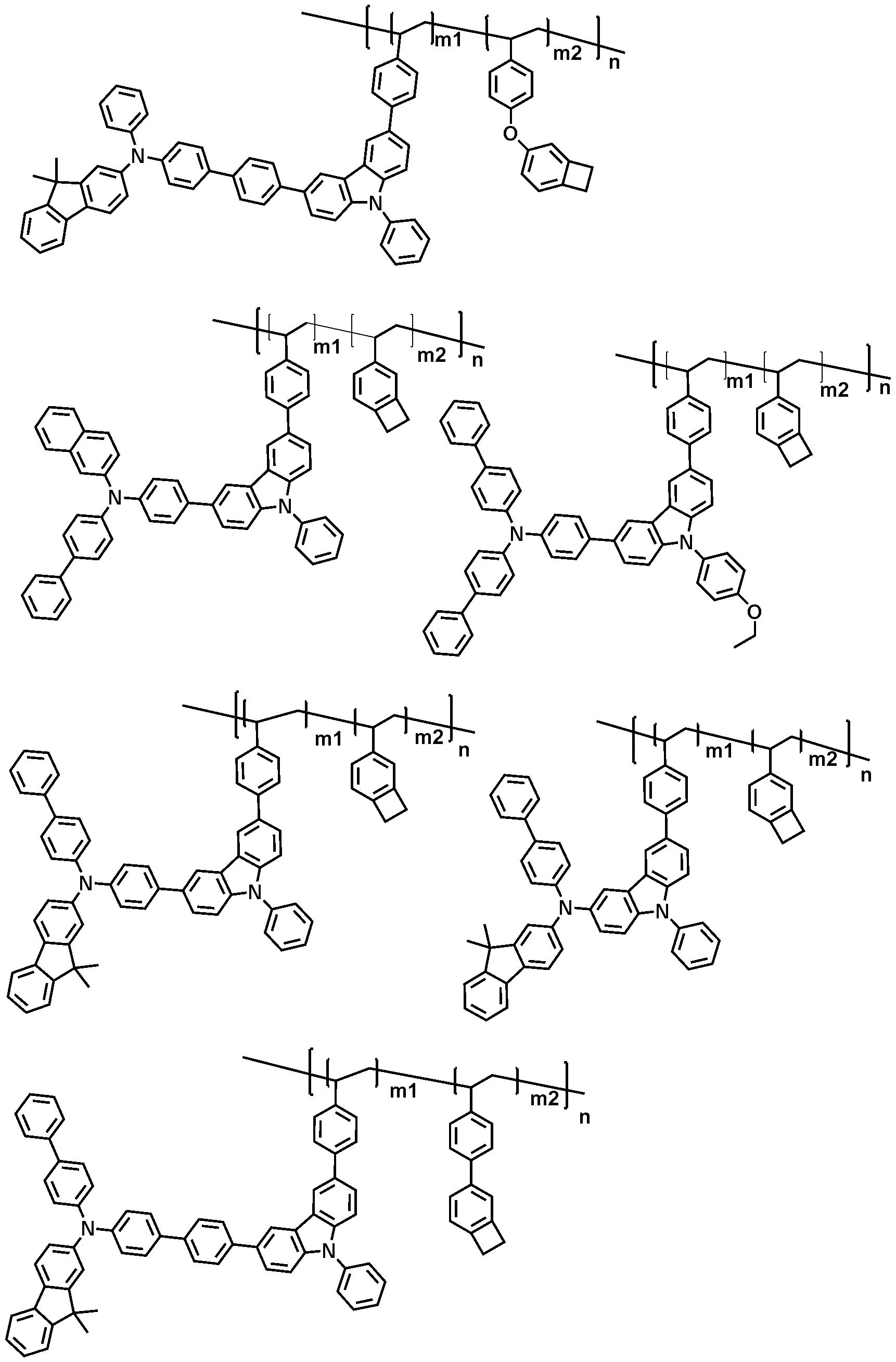
상기 구조에 있어서,
m1은 몰분율로서 0 < m1 < 1 이고,
m2는 몰분율로서 0 < m2 < 1 이며,
m1+m2≤1이고,
n은 단위의 반복수로서, 1 내지 10,000의 정수이다.
본 명세서의 일 실시상태에 있어서, 상기 화학식 1로 표시되는 제1 단위 및 상기 화학식 2로 표시되는 제2 단위를 포함하는 중합체는 하기 구조들 중에서 선택되는 어느 하나일 수 있다.


본 명세서의 일 실시상태에 있어서, 상기 중합체의 수평균 분자량은 5,000 g/mol 내지 1,000,000 g/mol 일 수 있다. 구체적으로는, 5,000 g/mol 내지 300,000 g/mol일 수 있다.
본 명세서에 있어서, 분자량 분석은 GPC 장비를 통해 분석하였다. 컬럼은 PL mixed Bx2를 사용하였고, 용매로는 테트라하이드로퓨란(THF) (0.45 m로 필터하여 사용)을 사용하였다. 1.0 mL/min의 유속과 1 mg/mL의 시료 농도로 측정하였다. 시료는 100 L 주입하였고, 컬럼 온도는 40℃로 설정하였다. 검출기(Detector)로는 Agilent RI detector를 사용하였고, PS(폴리스티렌)로 기준을 설정하였다. ChemStation 프로그램을 통해 데이터 프로세싱(Data processing)을 수행하였다.
본 명세서의 일 실시상태에 따른 중합체는 후술하는 제조 방법으로 제조될 수 있다. 후술하는 제조예들에서는 대표적인 예시들을 기재하지만, 필요에 따라, 치환기를 추가하거나 제외할 수 있으며, 치환기의 위치를 변경할 수 있다. 또한, 당기술분야에 알려져 있는 기술을 기초로, 출발물질, 반응물질, 반응 조건 등을 변경할 수 있다.
예컨대, 상기 화학식 1로 표시되는 제1 단위 및 상기 화학식 2로 표시되는 제2 단위를 포함하는 중합체는 하기 반응식 1과 같이 제조될 수 있다.
[반응식 1]

X, L1 내지 L6, b1, b2, Ar1 내지 Ar3, R1 내지 R8, r4, r5, m1 및 m2에 대한 정의는 상기 화학식 1 및 2에서 정의한 바와 동일하다.
본 명세서는 상기 중합체를 포함하는 코팅 조성물을 제공한다.
본 명세서의 일 실시상태에 따르면, 상기 코팅 조성물의 제조시에 아조비스이소부티로니트릴(azobisisobutyronitrile; AIBN)을 사용한다.
본 명세서의 일 실시상태에 따르면, 상기 코팅 조성물은 용매를 더 포함할 수 있다.
본 명세서의 일 실시상태에 있어서, 상기 코팅 조성물은 액상일 수 있다. 상기 "액상"은 상온 및 상압에서 액체 상태인 것을 의미한다.
본 명세서의 일 실시상태에 있어서, 상기 용매는 예컨대, 클로로포름, 염화메틸렌, 1,2-디클로로에탄, 1,1,2-트리클로로에탄, 클로로벤젠, o-디클로로벤젠 등의 염소계 용매; 테트라히드로푸란, 디옥산 등의 에테르계 용매; 톨루엔, 크실렌, 트리메틸벤젠, 메시틸렌 등의 방향족 탄화수소계 용매; 시클로헥산, 메틸시클로헥산, n-펜탄, n-헥산, n-헵탄, n-옥탄, n-노난, n-데칸 등의 지방족 탄화수소계 용매; 아세톤, 메틸에틸케톤, 시클로헥사논 등의 케톤계 용매; 아세트산에틸, 아세트산부틸, 에틸셀로솔브아세테이트 등의 에스테르계 용매; 에틸렌글리콜, 에틸렌글리콜모노부틸에테르, 에틸렌글리콜모노에틸에테르, 에틸렌글리콜모노메틸에테르, 디메톡시에탄, 프로필렌글리콜, 디에톡시메탄, 트리에틸렌글리콜모노에틸에테르, 글리세린, 1,2-헥산디올 등의 다가 알코올 및 그의 유도체; 메탄올, 에탄올, 프로판올, 이소프로판올, 시클로헥산올 등의 알코올계 용매; 디메틸술폭시드 등의 술폭시드계 용매;및 N-메틸-2-피롤리돈, N,N-디메틸포름아미드 등의 아미드계 용매; 메틸 벤조에이트, 부틸 벤조에이트, 3-페녹시 벤조에이트 등의 벤조에이트계 용매; 테트랄린 등의 용매가 예시되나, 본 명세서의 일 실시상태에 따른 화합물을 용해 또는 분산시킬 수 있는 용매라면 가능하며, 이들로 한정되는 것은 아니다.
본 명세서의 일 실시상태에 있어서, 상기 코팅 조성물은 톨루엔 용매를 포함한다.
또 하나의 실시상태에 있어서, 상기 용매는 1 종 단독으로 사용하거나, 또는 2 종 이상의 용매를 혼합하여 사용할 수 있다.
또 하나의 실시상태에 있어서, 상기 용매의 비점은 바람직하게 40℃ 내지 250℃, 더욱 바람직하게는 60℃ 내지 230℃이나, 이에 한정되는 것은 아니다.
또 하나의 실시상태에 있어서, 상기 단독 혹은 혼합 용매의 점도는 바람직하게 1 CP 내지 10 CP, 더욱 바람직하게는 3 CP 내지 8 CP 이나, 이에 한정되는 것은 아니다.
또 하나의 실시상태에 있어서, 상기 코팅 조성물의 농도는 바람직하게 0.1 wt/v% 내지 20 wt/v%, 더욱 바람직하게는 0.5 wt/v% 내지 5 wt/v% 이나, 이에 한정되는 것은 아니다.
본 명세서의 일 실시상태에 있어서, 상기 코팅 조성물은 열중합 개시제 및 광중합 개시제로 이루어진 군에서 선택되는 1종 또는 2종 이상의 첨가제를 더 포함할 수 있다.
상기 열중합 개시제는 메틸 에틸 케톤퍼옥사이드, 메틸 이소부틸 케톤퍼옥사이드, 아세틸아세톤퍼옥사이드, 메틸사이클로헥사논 퍼옥사이드, 시클로헥사논 퍼옥사이드, 이소부티릴 퍼옥사이드, 2,4-디클로로벤조일 퍼옥사이드, 비스-3,5,5-트리메틸 헥사노일 퍼옥사이드, 라우릴 퍼옥사이드, 벤조일 퍼옥사이드, p-크롤 벤조일 퍼옥사이드, 디큐밀퍼옥시드, 2,5-디메틸-2,5-(t-부틸 옥시)-헥산, 1,3-비스(t-부틸 퍼옥시-이소프로필) 벤젠, t-부틸 쿠밀(cumyl) 퍼옥사이드, 디-t부틸 퍼옥사이드, 2,5-디메틸-2,5-(디t-부틸 퍼옥시) 헥산-3, 트리스-(t-부틸 퍼옥시) 트리아진, 1,1-디t-부틸 퍼옥시-3,3,5-트리메틸 시클로헥산, 1,1-디t-부틸 퍼옥시 시클로헥산, 2,2-디(t-부틸 퍼옥시)부탄, 4,4-디-t-브치르파오키시바레릭크앗시드 n-부틸 에스테르, 2,2-비스(4,4-t-부틸 퍼옥시 사이클로헥실)프로판, t-부틸퍼옥시이소부틸레이트, 디t-부틸 퍼옥시 헥사하이드로 테레프탈레이트, t-부틸 퍼옥시-3,5,5-트리메틸헥사에이트, t-부틸퍼옥시벤조에이트, 디t-부틸 퍼옥시 트리메틸 아디페이트 등의 과산화물, 혹은 아조비스 이소부틸니트릴, 아조비스디메틸발레로니트릴, 아조비스 시클로헥실 니트릴 등의 아조계가 있으나, 이에 한정되는 것은 아니다.
상기 광중합 개시제는 디에톡시 아세토페논, 2,2-디메톡시-1,2-디페닐 에탄-1-온,1-하이드록시-사이클로헥실-페닐-케톤,4-(2-히드록시에톡시) 페닐-(2-하이드록시-2-프로필)케톤,2-벤질-2-디메틸아미노-1-(4-모르폴리노페닐)부타논-1,2-하이드록시-2-메틸-1-페닐프로판-1-온,2-메틸-2-모르폴리노(4-메틸 티오페닐) 프로판-1-온,1-페닐-1,2-프로판디온-2-(o-에톡시카르보닐)옥심, 등의 아세토페논계 또는 케탈계 광중합 개시제, 벤조인, 벤조인메치르에이텔, 벤조인에치르에이텔, 벤조인이소브치르에이텔, 벤조인이소프로피르에이텔 등의 벤조인에테르계 광중합 개시제, 벤조페논,4-하이드록시벤조페논, 2-벤조일나프탈렌,4-벤조일 비페닐,4-벤조일페닐에테르, 아크릴화벤조페논, 1,4-벤조일 벤젠, 등의 벤조페논계 광중합 개시제,2-이소프로필티옥산톤,2-클로로티옥산톤, 2,4-디메틸 티옥산톤, 2,4-디에틸티옥산톤, 2,4-디클로로티옥산톤 등의 티옥산톤계 광중합 개시제가 있으며, 기타 광중합 개시제로서는, 에틸 안트라퀴논, 2,4,6-트리메틸벤조일 디페닐 포스핀옥사이드, 2,4,6-트리메틸벤조일 페닐 에톡시 포스핀옥사이드, 비스(2,4,6-트리메틸벤조일)페닐 포스핀옥사이드, 비스(2,4-디메톡시 벤조일)-2,4,4-트리메틸 펜틸포스핀 옥사이드, 메치르페니르그리오키시에스텔, 9,10-페난트렌, 아크리딘계 화합물, 트리아진계 화합물, 이미다졸계 화합물을 들 수 있으나, 이에 한정되는 것은 아니다.
또한, 광중합 촉진 효과를 가지는 것을 단독 또는 상기 광 중합 개시제와 병용해 이용할 수도 있다. 예를 들면, 트리에탄올아민, 메틸 디에탄올 아민,4-디메틸아미노 안식향산 에틸,4-디메틸아미노 안식향산 이소아밀, 안식향산(2-디메틸아미노) 에틸, 4,4'-디메틸아미노벤조페논 등이 있으나, 이에 한정되는 것은 아니다.
본 명세서의 일 실시상태에 따르면, 상기 코팅 조성물은 니트록사이드 매개 중합(NMP), 원자 이동 라디칼 중합(ATRP), 가역적 첨가 해리 연쇄이동 중합(RAFT)과 같은 프리 라디칼 중합반응을 통하여 경화된다.
본 명세서는 또한, 상기 코팅 조성물을 이용하여 형성된 유기 발광 소자를 제공한다.
본 명세서의 일 실시상태에 있어서, 상기 유기 발광 소자는 제1 전극; 상기 제1 전극과 대향하여 구비된 제2 전극; 및 상기 제1 전극과 상기 제2 전극 사이에 구비된 1층 이상의 유기물층을 포함하고, 상기 유기물층 중 1층 이상은 상기 코팅 조성물의 경화물을 포함한다.
본 명세서의 일 실시상태에 있어서, 상기 제1 전극은 캐소드이고, 상기 제2 전극은 애노드이다.
또 하나의 실시상태에 있어서, 상기 제1 전극은 애노드이고, 상기 제2 전극은 캐소드이다.
본 명세서의 일 실시상태에 있어서, 상기 코팅 조성물의 경화물은 상기 코팅 조성물을 열처리 또는 광처리에 의하여 경화된 상태이다.
본 명세서의 일 실시상태에 있어서, 상기 코팅 조성물의 경화물을 포함하는 유기물층은 정공 수송층, 정공 주입층 또는 정공 수송과 정공 주입을 동시에 하는 층이다.
본 명세서의 일 실시상태에 있어서, 상기 코팅 조성물의 경화물을 포함하는 유기물층은 발광층을 포함하고, 상기 발광층은 상기 코팅 조성물의 경화물을 포함한다.
본 명세서의 일 실시상태에 있어서, 상기 코팅 조성물은 p 도핑 물질(p 도펀트)을 더 포함할 수 있다.
본 명세서의 일 실시상태에 있어서, 상기 p 도핑 물질은 F4TCNQ; 또는 붕소 음이온을 포함한다.
본 명세서의 일 실시상태에 있어서, 상기 p 도핑 물질은 F4TCNQ; 또는 붕소 음이온을 포함하고, 상기 붕소 음이온은 할로겐기를 포함한다.
본 명세서의 일 실시상태에 있어서, 상기 p 도핑 물질은 F4TCNQ; 또는 붕소 음이온을 포함하고, 상기 붕소 음이온은 F를 포함한다.
본 명세서의 일 실시상태에 있어서, 상기 p 도핑 물질은 하기 구조식 중에서 선택된다.

본 명세서의 일 실시상태에 있어서, 상기 코팅 조성물 총 중량 100% 기준으로, 상기 p 도핑 물질의 함량은 0.001 중량% 내지 50 중량%; 0.01 중량% 내지 30 중량%; 또는 1 중량% 내지 25 중량% 이다.
본 명세서의 일 실시상태에 있어서, 상기 유기 발광 소자는 정공 주입층, 정공 수송층. 전자 수송층, 전자 주입층, 전자 저지층 및 정공 저지층으로 이루어진 군에서 선택되는 1층 또는 2층 이상을 더 포함할 수 있다.
또 하나의 실시상태에 있어서, 유기 발광 소자는 기판 상에 애노드, 1층 이상의 유기물층 및 캐소드가 순차적으로 적층된 구조(normal type)의 유기 발광 소자일 수 있다.
또 하나의 실시상태에 있어서, 유기 발광 소자는 기판 상에 캐소드, 1층 이상의 유기물층 및 애노드가 순차적으로 적층된 역방향 구조(inverted type)의 유기 발광 소자일 수 있다.
본 명세서의 유기 발광 소자의 유기물층은 단층 구조로 이루어질 수도 있으나, 2층 이상의 유기물층이 적층된 다층 구조로 이루어질 수 있다. 예컨대, 본 명세서의 유기 발광 소자는 유기물층으로서 정공 주입층, 정공 수송층, 발광층, 전자 수송층, 전자 주입층 등을 포함하는 구조를 가질 수 있다. 그러나 유기 발광 소자의 구조는 이에 한정되지 않고 더 적은 수의 유기층을 포함할 수 있다.
예컨대, 본 명세서의 일 실시상태에 따른 유기 발광 소자의 구조는 도 1에 예시되어 있다.
상기 도 1에는 기판(101) 상에 애노드(201), 정공 주입층(301), 정공 수송층(401), 발광층(501), 전자 주입 및 수송을 동시에 하는 층(601) 및 캐소드(701)가 순차적으로 적층된 유기 발광 소자의 구조가 예시되어 있다.
본 명세서의 일 실시상태에 있어서, 상기 도 1의 정공 주입층(301), 정공 수송층(401) 또는 발광층(501)은 상기 화학식 1로 표시되는 제1 단위; 및 하기 화학식 2로 표시되는 제2 단위를 포함하는 중합체를 포함하는 코팅 조성물을 이용하여 형성될 수 있다.
본 명세서의 일 실시상태에 있어서, 상기 도 1의 정공 주입층(301)은 상기 화학식 1로 표시되는 제1 단위; 및 하기 화학식 2로 표시되는 제2 단위를 포함하는 중합체를 포함하는 코팅 조성물을 이용하여 형성될 수 있다.
본 명세서의 일 실시상태에 있어서, 상기 도 1의 정공 수송층(401)은 상기 화학식 1로 표시되는 제1 단위; 및 하기 화학식 2로 표시되는 제2 단위를 포함하는 중합체를 포함하는 코팅 조성물을 이용하여 형성될 수 있다.
상기 도 1은 유기 발광 소자를 예시한 것이며 이에 한정되지 않는다.
상기 유기 발광 소자가 복수개의 유기물층을 포함하는 경우, 상기 유기물층은 동일한 물질 또는 다른 물질로 형성될 수 있다.
본 명세서의 유기 발광 소자는 유기물층 중 1층 이상이 코팅 조성물을이용하여 형성되는 것을 제외하고는 당 기술분야에 알려져 있는 재료와 방법으로 제조될 수 있다.
예컨대, 본 명세서의 유기 발광 소자는 기판 상에 애노드, 유기물층 및 캐소드를 순차적으로 적층시켜 제조할 수 있다. 이 때, 스퍼터링법(sputtering)이나 전자빔 증발법(e-beam evaporation)과 같은 PVD(physical Vapor Deposition)방법을 이용하여, 기판 상에 금속 또는 전도성을 가지는 금속 산화물 또는 이들의 합금을 증착시켜 애노드를 형성하고, 그 위에 정공 주입층, 정공 수송층, 발광층 및 전자 수송층을 포함하는 유기물층을 형성한 후, 그 위에 캐소드로 사용할 수 있는 물질을 증착시켜 제조될 수 있다. 이와 같은 방법 외에도, 기판 상에 캐소드 물질부터 유기물층 및 애노드 물질을 차례로 증착시켜 유기 발광 소자를 제조할 수 있다.
본 명세서는 또한, 상기 코팅 조성물을 이용하여 형성된 유기 발광 소자의 제조 방법을 제공한다.
구체적으로, 본 명세서의 일 실시상태에 있어서, 기판을 준비하는 단계; 상기 기판 상에 캐소드 또는 애노드를 형성하는 단계; 상기 캐소드 또는 애노드 상에 1층 이상의 유기물층을 형성하는 단계; 및 상기 유기물층 상에 애노드 또는 캐소드를 형성하는 단계를 포함하고, 상기 유기물층을 형성하는 단계는 상기 코팅 조성물을 이용하여 1층 이상의 유기물층을 형성하는 단계를 포함하는 것인 유기 발광 소자의 제조 방법을 제공한다.
본 명세서의 일 실시상태에 있어서, 상기 코팅 조성물을 이용하여 형성된 유기물층은 스핀 코팅 또는 잉크젯팅을 이용하여 형성된다.
또 다른 실시상태에 있어서, 상기 코팅 조성물을 이용하여 형성된 유기물층은 인쇄법에 의하여 형성된다.
본 명세서의 상태에 있어서, 상기 인쇄법은 예컨대, 잉크젯 프린팅, 노즐 프린팅, 오프셋 프린팅, 전사 프린팅 또는 스크린 프린팅 등이 있으나, 이에 한정되는 것은 아니다.
본 명세서의 일 실시상태에 따른 코팅 조성물은 구조적인 특성으로 용액공정이 적합하여 인쇄법에 의하여 형성될 수 있으므로 소자의 제조 시에 시간 및 비용적으로 경제적인 효과가 있다.
본 명세서의 일 실시상태에 있어서, 상기 코팅 조성물을 이용하여 형성된 유기물층을 형성하는 단계는 상기 캐소드 또는 애노드 상에 상기 코팅 조성물을 코팅하는 단계; 및 상기 코팅된 코팅 조성물을 열처리 또는 광처리 하는 단계를 포함한다.
본 명세서의 일 실시상태에 있어서, 상기 코팅 조성물을 이용하여 형성된 유기물층을 열처리하는 시간은 바람직하게 1시간 이내, 더욱 바람직하게 30분 이내이다.
본 명세서의 일 실시상태에 있어서, 상기 코팅 조성물을 이용하여 형성된 유기물층을 열처리하는 분위기는 바람직하게 아르곤, 질소 등의 불활성 기체이다.
상기 코팅 조성물을 이용하여 형성된 유기물층을 형성하는 단계에서 상기 열처리 또는 광처리 단계를 포함하는 경우에는 코팅 조성물에 포함된 복수 개의 플루오렌기가 가교를 형성하여 박막화된 구조가 포함된 유기물층을 제공할 수 있다. 이 경우, 상기 코팅 조성물을 이용하여 형성된 유기물층의 표면 위에 증착된 용매에 의하여 용해되거나, 형태학적으로 영향을 받거나 분해되는 것을 방지할 수 있다.
따라서, 상기 코팅 조성물을 이용하여 형성된 유기물층이 열처리 또는 광처리 단계를 포함하여 형성된 경우에는 용매에 대한 저항성이 증가하여 용액 증착 및 가교 방법을 반복 수행하여 다층을 형성할 수 있으며, 안정성이 증가하여 소자의 수명 특성을 증가시킬 수 있다.
본 명세서의 일 실시상태에 있어서, 상기 중합체를 포함하는 코팅 조성물은 고분자 결합제에 혼합하여 분산시킨 코팅 조성물을 이용할 수 있다.
본 명세서의 일 실시상태에 있어서, 고분자 결합제로서는, 전하 수송을 극도로 저해하지 않는 것이 바람직하고, 또한 가시광에 대한 흡수가 강하지 않은 것이 바람직하게 이용된다. 고분자 결합제로서는, 폴리(N-비닐카르바졸), 폴리아닐린 및 그의 유도체, 폴리티오펜 및 그의 유도체, 폴리(p-페닐렌비닐렌) 및 그의 유도체, 폴리(2,5-티에닐렌비닐렌) 및 그의 유도체, 폴리카보네이트, 폴리아크릴레이트, 폴리메틸아크릴레이트, 폴리메틸메타크릴레이트, 폴리스티렌, 폴리염화비닐, 폴리실록산 등이 예시된다.
또한, 본 명세서의 일 실시상태에 따른 중합체는 유기물층에 화합물 단독으로 포함할 수도 있고, 다른 모노머와 혼합한 코팅 조성물을 사용하여 공중합체로서 포함시킬 수 있다. 또한, 다른 고분자와 혼합한 코팅 조성물을 사용하여 공중합체, 또는 혼합물을 포함할 수 있다.
상기 애노드 물질로는 통상 유기물층으로 정공 주입이 원활할 수 있도록 일함수가 큰 물질이 바람직하다. 본 명세서에서 사용될 수 있는 애노드 물질의 구체적인 예로는 바나듐, 크롬, 구리, 아연, 금과 같은 금속 또는 이들의 합금; 아연 산화물, 인듐 산화물, 인듐주석 산화물(ITO), 인듐아연 산화물(IZO)과 같은 금속 산화물; ZnO:Al 또는 SnO2 : Sb와 같은 금속과 산화물의 조합; 폴리(3-메틸티오펜), 폴리[3,4-(에틸렌-1,2-디옥시)티오펜](PEDOT), 폴리피롤 및 폴리아닐린과 같은 전도성 고분자 등이 있으나, 이들에만 한정되는 것은 아니다.
상기 캐소드 물질로는 통상 유기물층으로 전자 주입이 용이하도록 일함수가 작은 물질인 것이 바람직하다. 캐소드 물질의 구체적인 예로는 마그네슘, 칼슘, 나트륨, 칼륨, 티타늄, 인듐, 이트륨, 리튬, 가돌리늄, 알루미늄, 은, 주석 및 납과 같은 금속 또는 이들의 합금; LiF/Al 또는 LiO2/Al과 같은 다층 구조 물질 등이 있으나, 이들에만 한정되는 것은 아니다.
상기 정공 주입층은 전극으로부터 정공을 주입하는 층으로, 정공 주입 물질로는 정공을 수송하는 능력을 가져 애노드에서의 정공 주입효과, 발광층 또는 발광재료에 대하여 우수한 정공 주입 효과를 갖고, 발광층에서 생성된 여기자의 전자 주입층 또는 전자 주입 재료에의 이동을 방지하며, 또한, 박막 형성 능력이 우수한 화합물이 바람직하다. 정공 주입 물질의 HOMO(highest occupied molecular orbital)가 애노드 물질의 일함수와 주변 유기물층의 HOMO 사이인 것이 바람직하다. 정공 주입 물질의 구체적인 예로는 금속 포피린(porphyrin), 올리고티오펜, 아릴아민 계열의 유기물, 헥사니트릴헥사아자트리페닐렌 계열의 유기물, 퀴나크리돈(quinacridone)계열의 유기물, 페릴렌(perylene) 계열의 유기물, 안트라퀴논 및 폴리아닐린과 폴리티오펜 계열의 전도성 고분자 등이 있으나, 이들에만 한정되는 것은 아니다.
상기 정공 수송층은 정공 주입층으로부터 정공을 수취하여 발광층까지 정공을 수송하는 층으로, 정공 수송 물질로는 애노드나 정공 주입층으로부터 정공을 수송받아 발광층으로 옮겨줄 수 있는 물질로 정공에 대한 이동성이 큰 물질이 적합하다. 구체적인 예로는 아릴아민 계열의 유기물, 전도성 고분자, 및 공액 부분과 비공액 부분이 함께 있는 블록 공중합체 등이 있으나, 이들에만 한정되는 것은 아니다.
상기 발광 물질로는 정공 수송층과 전자 수송층으로부터 정공과 전자를 각각 수송받아 결합시킴으로써 가시광선 영역의 빛을 낼 수 있는 물질로서, 형광이나 인광에 대한 양자 효율이 좋은 물질이 바람직하다. 구체적인 예로는 8-히드록시-퀴놀린 알루미늄 착물(Alq3); 카르바졸 계열 화합물; 이량체화 스티릴(dimerized styryl) 화합물; BAlq; 10-히드록시벤조 퀴놀린-금속 화합물; 벤족사졸, 벤즈티아졸 및 벤즈이미다졸 계열의 화합물; 폴리(p-페닐렌비닐렌)(PPV) 계열의 고분자; 스피로(spiro) 화합물; 폴리플루오렌; 또는 루브렌 등이 있으나, 이들에만 한정되는 것은 아니다.
상기 발광층은 호스트 재료 및 도펀트 재료를 포함할 수 있다. 호스트 재료는 축합 방향족환 유도체 또는 헤테로환 함유 화합물 등이 있다. 구체적으로 축합 방향족환 유도체로는 안트라센 유도체, 피렌 유도체, 나프탈렌 유도체, 펜타센 유도체, 페난트렌 화합물, 플루오란텐 화합물 등이 있고, 헤테로환 함유 화합물로는 카바졸 유도체, 디벤조퓨란 유도체, 래더형 퓨란 화합물, 피리미딘 유도체 등이 있으나, 이에 한정되지 않는다.
도펀트 재료로는 방향족 아민 유도체, 스트릴아민 화합물, 붕소 착체, 플루오란텐 화합물, 금속 착체 등이 있다. 구체적으로 방향족 아민 유도체로는 치환 또는 비치환된 아릴아민기를 갖는 축합 방향족환 유도체로서, 아릴아민기를 갖는 피렌, 안트라센, 크리센, 페리플란텐 등이 있으며, 스티릴아민 화합물로는 치환 또는 비치환된 아릴아민에 적어도 1개의 아릴비닐기가 치환되어 있는 화합물로, 아릴기, 실릴기, 알킬기, 시클로알킬기 및 아릴아민기로 이루어진 군에서 1 또는 2 이상 선택되는 치환기가 치환 또는 비치환된다. 구체적으로 스티릴아민, 스티릴디아민, 스티릴트리아민, 스티릴테트라아민 등이 있으나, 이에 한정되지 않는다. 또한, 금속 착체로는 이리듐 착체, 백금 착체 등이 있으나, 이에 한정되지 않는다.
상기 전자 수송층은 전자 주입층으로부터 전자를 수취하여 발광층까지 전자를 수송하는 층으로 전자 수송 물질로는 캐소드로부터 전자를 잘 주입 받아 발광층으로 옮겨줄 수 있는 물질로서, 전자에 대한 이동성이 큰 물질이 적합하다. 구체적인 예로는 8-히드록시퀴놀린의 Al착물; Alq3를 포함한 착물; 유기 라디칼 화합물; 또는 히드록시플라본-금속 착물 등이 있으나, 이들에만 한정되는 것은 아니다. 전자 수송층은 종래기술에 따라 사용된 바와 같이 임의의 원하는 캐소드 물질과 함께 사용할 수 있다. 특히, 적절한 캐소드 물질의 예는 낮은 일함수를 가지고 알루미늄층 또는 실버층이 뒤따르는 통상적인 물질이다. 구체적으로 세슘, 바륨, 칼슘, 이테르븀 및 사마륨이고, 각 경우 알루미늄 층 또는 실버층이 뒤따른다.
상기 전자 주입층은 전극으로부터 전자를 주입하는 층으로, 전자를 수송하는 능력을 갖고, 캐소드로부터의 전자주입 효과, 발광층 또는 발광 재료에 대하여 우수한 전자주입 효과를 가지며, 발광층에서 생성된 여기자의 정공 주입층에의 이동을 방지하고, 또한, 박막형성능력이 우수한 화합물이 바람직하다. 구체적으로는 플루오레논, 안트라퀴노다이메탄, 다이페노퀴논, 티오피란 다이옥사이드, 옥사졸, 옥사다이아졸, 트리아졸, 이미다졸, 페릴렌테트라카복실산, 프레오레닐리덴 메탄, 안트론 등과 그들의 유도체, 금속 착체 화합물 및 함질소 5원환 유도체 등이 있으나, 이에 한정되지 않는다.
상기 금속 착체 화합물로서는 8-하이드록시퀴놀리나토 리튬, 비스(8-하이드록시퀴놀리나토)아연, 비스(8-하이드록시퀴놀리나토)구리, 비스(8-하이드록시퀴놀리나토)망간, 트리스(8-하이드록시퀴놀리나토)알루미늄, 트리스(2-메틸-8-하이드록시퀴놀리나토)알루미늄, 트리스(8-하이드록시퀴놀리나토)갈륨, 비스(10-하이드록시벤조[h]퀴놀리나토)베릴륨, 비스(10-하이드록시벤조[h]퀴놀리나토)아연, 비스(2-메틸-8-퀴놀리나토)클로로갈륨, 비스(2-메틸-8-퀴놀리나토)(o-크레졸라토)갈륨, 비스(2-메틸-8-퀴놀리나토)(1-나프톨라토)알루미늄, 비스(2-메틸-8-퀴놀리나토)(2-나프톨라토)갈륨 등이 있으나, 이에 한정되지 않는다.
상기 정공 저지층은 정공의 캐소드 도달을 저지하는 층으로, 일반적으로 전자 주입층과 동일한 조건으로 형성될 수 있다. 구체적으로 옥사디아졸 유도체나 트리아졸 유도체, 페난트롤린 유도체, 알루미늄 착물 (aluminum complex) 등이 있으나, 이에 한정되지 않는다.
본 명세서에 따른 유기 발광 소자는 사용되는 재료에 따라 전면 발광형, 후면 발광형 또는 양면 발광형일 수 있다.
본 명세서의 일 실시상태에 있어서, 상기 화합물은 유기 발광 소자 외에도 유기 태양 전지 또는 유기 트랜지스터에 포함될 수 있다.
이하, 본 명세서를 구체적으로 설명하기 위해 실시예를 들어 상세하게 설명하기로 한다. 그러나, 본 명세서에 따른 실시예들은 여러 가지 다른 형태로 변형될 수 있으며, 본 명세서의 범위가 아래에서 기술하는 실시예들에 한정되는 것으로 해석되지 않는다. 본 명세서의 실시예들은 당업계에서 평균적인 지식을 가진 자에게 본 명세서를 보다 완전하게 설명하기 위해 제공되는 것이다.
<제조예 1. 중간체 제조>
(1) 중간체 5의 제조

3-브로모-9-페닐-9H-카바졸(9 g, 27.9mmol) 및 4-포르밀벤젠 보론산(4.18 g, 27.9 mmol)을 무수 테트라하이드로퓨란(THF, 100 mL)에 녹인 후, Pd(PPh3)4 (0.32 g, 0.28 mmol)과 2M 탄산칼륨(K2CO3/H20)수용액 70ml을 넣고 6시간 동안 환류시켰다. 반응 용액을 상온으로 식힌 후, 유기층을 추출하였다. 반응액을 농축시키고 에틸알코올(EtOH)로 재결정하여 중간체 3(8.9 g, 수율 92%)을 얻었다. MS: [M+H]+ = 348
상기 중간체 3(8.2 g, 23.6 mmol)을 다이메틸포름알데하이드(200mL)에 녹이고, N-브로모 숙신이미드(4.15 g, 23.6 mmol)를 첨가한 후, 5시간 상온에서 교반 하였다. 반응 용액에 증류수를 넣어 반응을 종료시킨 후, 유기층을 추출하였다. 반응액을 농축시키고 에틸알코올(EtOH)로 재결정하여 중간체 4 (8.25 g, 수율 82%)를 얻었다. MS: [M+H]+ = 427
메틸트리페닐포스포늄 브로마이드 염 (13.41g, 37.532mmol) 및 포타슘 t-부톡사이드(4.21g, 37.532mmol)를 무수 테트라하이드로퓨란(300ml)에 넣어 먼저 교반 하였다. 이후, 무수테트라하이드로퓨란(60ml)에 녹인 중간체 4(8g, 18.766mmol)를 천천히 적가한 후 5시간동안 반응시켰다. 탄산나트륨수용액으로 반응을 종료시킨 후, 메틸렌클로라이드와 물을 사용하여 유기층으로 추출하고 잔여 수분을 MgSO4를 사용해 제거했다. 반응액을 농축시킨 후 메틸렌클로라이드와 헥세인을 이용하여 컬럼크로마토그래피하여 중간체 5(7.8g, 98%)를 얻었다. MS: [M+H]+ = 425
(2) 중간체 6의 제조

상기 중간체 5(2g, 4.713mmol) 및 (4-클로로페닐)보론산(1.1g, 7.069mmol)을 무수 테트라하이드로퓨란(THF, 20ml)에 녹인 후, Pd(PPh3)4 (0.32 g, 0.28 mmol)과 2M 탄산칼륨(K2CO3/H20)수용액 15ml을 넣고 6시간 동안 환류시켰다. 반응 용액을 상온으로 식힌 후, 유기층을 추출하였다. 반응액을 농축시키고 에틸알코올(EtOH)로 재결정하여 중간체 6 (2 g, 수율 93%)을 얻었다. MS: [M+H]+ =457
<제조예 2. 화합물 A1 내지 A9의 제조>
(1) 화합물 A1의 제조

중간체 5(3.65g, 8.615mmol), 4-(다이페닐아미노)페닐 보론산(2.99g, 10.338mmol), Pd(PPh3)4(498mg, 0.431mmol) 및 K2CO3(3.57g, 25.845mmol)을 무수 테트라하이드로퓨란(200ml) 및 증류수(100ml)에 녹인 후, 70℃에서 15시간 교반 하였다. 에틸아세테이트와 물을 이용하여 유기층을 추출했다. 이를 MgSO4를 이용하여 수분을 제거한 후, 감압하여 용매를 제거했다. 얻어진 물질을 에틸아세테이트와 헥세인을 사용하여 컬럼크로마토그래피하여 화합물 A1를 분리 및 정제했다. MS: [M+H]+ = 589
(2) 화합물 A2의 제조

4-(다이페닐아미노)페닐 보론산 대신에 4-(다이바이페닐-4-일마이노)페닐 보론산을 사용한 것을 제외하고, 상기 화합물 A1을 제조한 방법과 동일한 방법으로 화합물 A2를 제조했다. MS: [M+H]+ = 741
(3) 화합물 A3의 제조

4-(다이페닐아미노)페닐 보론산 대신에 4-(바이페닐-4-일(9,9-다이메틸-9H-플루오렌-2-일)아미노)페닐 보론산을 사용한 것을 제외하고, 상기 화합물 A1을 제조한 방법과 동일한 방법으로 화합물 A3을 제조했다. MS: [M+H]+ = 782
(4) 화합물 A4의 제조

중간체 5(3.65g, 8.615mmol), 다이페닐아민(1.74g, 10.338mmol), Pd(tBu3P)2(220mg, 0.431mmol) 및 소듐 t-부톡사이드(2.48g, 25.845mmol)을 톨루엔(26ml)에 녹인 후, 100℃에서 15시간 교반 하였다. 에틸아세테이트와 물을 이용하여 유기층을 추출했다. 이를 MgSO4를 이용하여 수분을 제거한 후, 감압하여 용매를 제거했다. 얻어진 물질을 에틸아세테이트와 헥세인을 사용하여 컬럼크로마토그래피하여 화합물 A4를 분리 및 정제했다. [M+H]+=513
(5) 화합물 A5의 제조

다이페닐아민 대신에 다이(바이페닐-4-일)아민을 사용한 것을 제외하고, 상기 화합물 A4을 제조한 방법과 동일한 방법으로 화합물 A5를 제조했다. MS: [M+H]+ = 665
(6) 화합물 A6의 제조

다이페닐아민 대신에 N-(바이페닐-4-일)-9,9-다이메틸-9H-플루오렌-2-아민을 사용한 것을 제외하고, 상기 화합물 A4을 제조한 방법과 동일한 방법으로 화합물 A6을 제조했다. MS: [M+H]+ = 705
(7) 화합물 A7의 제조

중간체 5 대신에 중간체 6을 사용한 것을 제외하고, 상기 화합물 A1을 제조한 방법과 동일한 방법으로 A7을 제조했다. MS: [M+H]+ = 665
(8) 화합물 A8의 제조

중간체 5 대신에 중간체 6을 사용한 것을 제외하고, 상기 화합물 A2를 제조한 방법과 동일한 방법으로 A8을 제조했다. MS: [M+H]+ = 817
(9) 화합물 A9의 제조

중간체 5 대신에 중간체 6을 사용한 것을 제외하고, 상기 화합물 A3을 제조한 방법과 동일한 방법으로 A9를 제조했다. MS: [M+H]+ = 857
<제조예 3. 화합물 B2 내지 B4의 제조>
(1) 화합물 B2의 제조

(4-포르밀페닐)보론산(4.91g, 32.778mmol) 및 3-브로모 바이시클로[4.2.0]옥타-1(6),2,4-트리엔(5g, 27.315mmol)을 Pd(PPh3)4(1.58g,1.366mmol), K2CO3(11.32g, 81.945mmol)을 무수 테트라하이드로퓨란 (200ml) 및 증류수(100ml)에 녹인 후, 70℃에서 15시간 교반 하였다. 에틸아세테이트와 물을 이용하여 유기층을 추출했다. 이를 MgSO4를 이용하여 수분을 제거한 후, 감압하여 용매를 제거했다. 얻어진 물질을 에틸아세테이트와 헥세인을 사용하여 컬럼크로마토그래피하여 중간체 7을 분리 및 정제했다. MS: [M+H]+ = 209
메틸트리페닐포스포늄 브로마이드 염 (13.41g, 37.532mmol) 및 포타슘 t-부톡사이드 (4.21g, 37.532mmol)를 무수 테트라하이드로퓨란(30ml)에 넣어 교반 하였다. 이후, 무수 테트라하이드로퓨란 (10ml)에 녹인 중간체 7(3.90g, 18.766mmol)을 천천히 적가한 후 4시간동안 반응시켰다. 탄산나트륨수용액으로 반응을 종료시킨 후, 메틸렌클로라이드와 물을 사용하여 유기층으로 추출하고 잔여 수분을 MgSO4를 사용해 제거했다. 반응액을 농축시킨 후 메틸렌클로라이드와 헥세인을 이용하여 컬럼크로마토그래피하여 화합물 B2(3.2g, 84%)를 제조했다. MS: [M+H]+ = 207
(2) 화합물 B3의 제조

N-페닐-4-비닐아닐린 (8g, 40.969mmol), 3-브로모 바이시클로[4.2.0]옥타-1(6),2,4-트리엔(7.61g, 45.588mmol), Pd(tBu3P)2(635mg, 1.243mmol) 및 소듐 t-부톡사이드 (9.95g, 103.61mmol)을 톨루엔(26ml)에 녹인 후, 100℃에서 15시간동안 교반 하였다. 에틸아세테이트와 물을 이용하여 유기층을 추출했다. 이를 MgSO4를 이용하여 수분을 제거한 후, 감압하여 용매를 제거했다. 얻어진 물질을 에틸아세테이트와 헥세인을 사용하여 컬럼크로마토그래피하여 화합물 B3를 분리 및 정제했다. MS: [M+H]+=298
(3) 화합물 B4의 제조

4-비닐페놀(3g, 24.968mmol), 3-브로모 바이시클로[4.2.0]옥타-1(6),2,4-트리엔(5.03g, 27.464mmol)에 포타슘카보네이트(6.9g, 49.936mmol)를 DMF 28ml에 넣고 140℃에서 20시간 교반했다. 에틸아세테이트와 물을 이용하여 유기층을 추출했다. 이를 MgSO4를 이용하여 수분을 제거한 후, 감압하여 용매를 제거했다. 얻어진 물질을 에틸아세테이트와 헥세인을 사용하여 컬럼크로마토그래피하여 화합물 B4(2.1g)를 분리 및 정제했다. MS: [M+H]+=222
<제조예 4. 중합체 C1 내지 C4의 제조>
(1) 중합체 C1의 제조

화합물 A1(500mg), 화합물 B2(94mg) 및 AIBN(1.2mg)을 톨루엔에 넣고, 질소치환하에 100℃에서 14시간동안 반응시켰다. 에틸아세테이트에 침전하여 제조된 중합체 C1을 제조했다. Mn=18,900 Mw=30,600
(2) 중합체 C2의 제조

화합물 A1 및 화합물 B2 대신에 화합물 A3 및 4-바이닐-1,2-다이하이드로부타벤젠을 사용한 것을 제외하고, 상기 중합체 C1을 제조한 방법과 동일한 방법으로 중합체 C2를 제조했다. Mn=25,700 Mw=47,900
(3) 중합체 C3의 제조

화합물 A1 및 화합물 B2 대신에 화합물 A6 및 4-바이닐-1,2-다이하이드로부타벤젠을 사용한 것을 제외하고, 상기 중합체 C1을 제조한 방법과 동일한 방법으로 중합체 C3을 제조했다. Mn=116,000 Mw=247,900
(4) 중합체 C4의 제조

화합물 A1 대신에 화합물 A9를 사용한 것을 제외하고, 상기 중합체 C1을 제조한 방법과 동일한 방법으로 중합체 C4를 제조했다. Mn=15,900 Mw=25,900
<실시예>
[ITO 기판의 준비]
ITO(indium tin oxide)가 1,500Å의 두께로 박막 코팅된 유리 기판을 세제를 녹인 증류수에 넣고 초음파로 세척하였다. 이 때, 세제로는 피셔사(Fischer Co.) 제품을 사용하였으며, 증류수로는 밀리포어사(Millipore Co.) 제품의 필터(Filter)로 2차로 걸러진 증류수를 사용하였다. ITO를 30분간 세척한 후, 증류수로 2회 반복하여 초음파 세척을 10분간 진행하였다.
증류수 세척이 끝난 후, 이소프로필 및 아세톤의 용제로 초음파 세척을 하고 건조시킨 후, 상기 기판을 5분간 세정한 후 글로브박스로 기판을 수송시켰다.
[소자예 1]
ITO 투명전극 위에 상기 중합체 C1: 하기 p 도펀트(하기 화학식 M) (8:2의 중량비)의 2wt% 톨루엔 잉크를 ITO 표면 위에 스핀 코팅(4000rpm)하고 200℃ 에서 30분간 열처리(경화)하여 40nm 두께로 정공 주입층을 형성하였다. 이후, 진공 증착기로 이송한 후, 상기 정공 주입층 위에 하기 화합물 G를 진공 증착하여 20nm 두께의 정공 수송층을 형성하였다.
이어서, 상기 정공 수송층 위에 하기 화합물 H와 화합물 I (9:1의 중량비)를 20nm의 두께로 진공 증착하여 발광층을 형성하였다. 상기 발광층 위에 화합물 J을 35nm의 두께로 진공 증착하여 전자 주입 및 수송을 동시에 하는 층을 형성하였다. 상기 전자 주입 및 수송을 동시에 하는 층 위에 순차적으로 1nm 두께로 LiF와 100nm 두께로 알루미늄을 증착하여 캐소드를 형성하였다.
상기의 과정에서 유기물의 증착 속도는 0.4 내지 0.7 Å/sec를 유지하였고, 캐소드의 리튬플루오라이드는 0.3 Å/sec, 알루미늄은 2 Å/sec의 증착 속도를 유지하였으며, 증착시 진공도는 2 X 10⁻⁷ 내지 5 X 10⁻⁸ torr를 유지하여, 유기 발광 소자를 제작하였다.
[화합물 G]

[화합물 H]

[화합물 I]

[화합물 J]

[화학식 M]

[소자예 2]
상기 소자예 1의 제작과정에서 정공 주입층 성막시 중합체 C1:p 도펀트(8:2 중량비) 2wt% 톨루엔 잉크 대신에 상기 중합체 C2:p 도펀트(8:2 중량비) 의 2wt% 톨루엔 잉크를 사용한 것을 제외하고는, 소자예 1의 과정과 동일한 방법으로 유기 발광 소자를 제조하였다.
[소자예 3]
상기 소자예 1의 제작과정에서 정공 주입층 성막시 중합체 C1:p 도펀트(8:2 중량비) 2wt% 톨루엔 잉크 대신에 상기 중합체 C3:p 도펀트(8:2 중량비) 의 2wt% 톨루엔 잉크를 사용한 것을 제외하고는, 소자예 1의 과정과 동일한 방법으로 유기 발광 소자를 제조하였다.
[소자예 4]
상기 소자예 1의 제작과정에서 정공 주입층 성막시 중합체 C1:p 도펀트(8:2 중량비) 2wt% 톨루엔 잉크 대신에 상기 중합체 C4:p 도펀트(8:2 중량비) 의 2wt% 톨루엔 잉크를 사용한 것을 제외하고는, 소자예 1의 과정과 동일한 방법으로 유기 발광 소자를 제조하였다.
[비교 소자예 1]
상기 소자예 1의 제작과정에서 정공 주입층 성막시 중합체 C1:p 도펀트(8:2 중량비) 2wt% 톨루엔 잉크 대신에 하기 중합체 F:p 도펀트(8:2 중량비)의 2wt% 톨루엔 잉크를 사용한 것을 제외하고는, 소자예 1의 과정과 동일한 방법으로 유기 발광 소자를 제조하였다.

[비교 소자예 2]
상기 소자예 1의 제작과정에서 정공 주입층 성막시 중합체 C1:p 도펀트(8:2 중량비) 2wt% 톨루엔 잉크 대신에 하기 중합체 Z:p 도펀트(8:2 중량비)의 2wt% 톨루엔 잉크를 사용한 것을 제외하고는, 소자예 1의 과정과 동일한 방법으로 유기 발광 소자를 제조하였다.

상기 소자예 1 내지 소자예 4 및 비교 소자예 1 및 2에서 제조된 유기 발광 소자에 전류를 인가하였을 때, 전압, 효율 및 수명을 측정하고 그 결과를 하기 [표 1]에 나타내었다. T95는 광밀도 20mA/cm2 에서의 초기 휘도를 100%로 하였을 때 휘도가 95%로 감소되는데 소요되는 시간을 의미한다. 또한, EQE는 전류 밀도가 10mA/cm2 가 되도록 소자에 전압을 인가했을 때의 분광 방사 휘도 스펙트럼을 분광 방사 휘도계 CS-1000 (코니카 미놀타사 제조)으로 계측한 값으로, 얻어진 상기 분광 방사 휘도 스펙트럼으로부터 외부 양자 효율을 산출하였다.
| 전압(V) (@10mA/cm2) | 전류밀도(mA/cm2) | EQE (%)(@10mA/cm2) | 수명(T95, h)(@20mA/cm2) | |
| 소자예 1 | 5.81 | 10 | 4.1 | 29 |
| 소자예 2 | 5.27 | 10 | 5.0 | 50 |
| 소자예 3 | 5.31 | 10 | 4.0 | 46 |
| 소자예 4 | 5.01 | 10 | 4.4 | 45 |
| 비교 소자예 1 | 7.23 | 10 | 2.1 | 20 |
| 비교 소자예 2 | 6.75 | 10 | 3.5 | 22 |
상기 표 1에서 보는 바와 같이, 본 명세서의 화학식 1로 표시되는 제1단위 및 화학식 2로 표시되는 제2 단위를 포함하는 중합체를 사용한 코팅 조성물을 정공 주입층 물질로 사용한 경우, 비교 소자예 1 및 2에 비하여, 동시에 효율과 수명이 우수한 효과를 보이는 것을 알 수 있다.
따라서, 본 명세서의 화학식 1로 표시되는 제1 단위 및 화학식 2로 표시되는 제2 단위를 포함하는 중합체를 사용한 코팅 조성물은 코팅층의 균일성 및 막의 안정성이 우수하므로, 상기 코팅 조성물을 이용하여 유기 발광 소자의 성능을 향상시켜 줄 수 있음을 알 수 있다.
이상을 통해 본 발명의 바람직한 실시예에 대하여 설명하였지만, 본 발명은 이에 한정되는 것이 아니고 특허청구범위와 발명의 상세한 설명의 범위 안에서 여러 가지로 변형하여 실시하는 것이 가능하고 이 또한 발명의 범주에 속한다.
Claims (15)
- 하기 화학식 1로 표시되는 제1 단위; 및하기 화학식 2로 표시되는 제2 단위를 포함하는 중합체:[화학식 1]
 [화학식 2]
 상기 화학식 1 및 2에 있어서,L1 내지 L6은 서로 같거나 상이하고, 각각 독립적으로 직접결합; -O-; 치환 또는 비치환된 알킬렌기; 치환 또는 비치환된 아릴렌기; 치환 또는 비치환된 2가의 아민기; 또는 치환 또는 비치환된 헤테로아릴렌기이며,b1 및 b2는 각각 1 내지 10의 정수이고,상기 b1 및 b2가 각각 2 이상일 때, 2 이상의 L1 및 L6은 각각 서로 같거나 상이하며,Ar1 내지 Ar3은 서로 같거나 상이하고, 각각 독립적으로 치환 또는 비치환된 알킬기; 치환 또는 비치환된 알콕시기; 치환 또는 비치환된 아릴옥시기; 치환 또는 비치환된 아릴기; 또는 치환 또는 비치환된 헤테로고리기이고,R1 내지 R8은 서로 같거나 상이하고, 각각 독립적으로 수소; 중수소; 할로겐기; 히드록시기; 니트릴기; 치환 또는 비치환된 알킬기; 치환 또는 비치환된 시클로알킬기; 치환 또는 비치환된 아릴기; 또는 치환 또는 비치환된 헤테로고리기이며,r4 및 r5는 각각 1 내지 3의 정수이고,상기 r4 및 r5가 각각 2 이상일 때, 2 이상의 R4 및 R5는 각각 서로 같거나 상이하며,m1은 몰분율로서 0 < m1 < 1 이고,m2는 몰분율로서 0 < m2 < 1 이며,m1+m2≤1이고,X는 하기 구조들 중에서 선택되는 어느 하나이며,
 상기 구조에 있어서,L11은 치환 또는 비치환된 알킬렌기; 또는 치환 또는 비치환된 아릴렌기이고,R10 내지 R13은 서로 같거나, 상이하고, 각각 독립적으로 수소; 또는 치환 또는 비치환된 탄소수 1 내지 6의 알킬기이고,X가인 경우, b2는 1 내지 3의 정수이다.
- 청구항 1에 있어서, 상기 화학식 1은 하기 화학식 103로 표시되는 것인 중합체:[화학식 103]
 상기 화학식 103에 있어서,L2 내지 L5, Ar1 내지 Ar3, R1 내지 R5, r4, r5 및 m1의 정의는 화학식 1에서 정의한 바와 같고,L101은 직접결합; -O-; 치환 또는 비치환된 알킬렌기; 치환 또는 비치환된 아릴렌기; 치환 또는 비치환된 2가의 아민기; 또는 치환 또는 비치환된 헤테로아릴렌기이며,b101은 1 내지 9 정수이고,상기 b101이 2 이상일 때, 2 이상의 L101은 각각 서로 같거나 상이하다.
 - 청구항 1에 있어서, Ar1은 알킬기; 알콕시기; 아릴옥시기; 아릴기; 및 헤테로고리기로 구성된 군에서 선택된 1개 이상의 치환기 또는 상기 군에서 선택된 2개 이상의 치환기가 연결된 치환기로 치환 또는 비치환된 탄소수 6 내지 30의 아릴기인 것인 중합체.
- 청구항 1에 있어서, Ar2 및 Ar3은 서로 같거나 상이하고, 각각 독립적으로 치환 또는 비치환된 페닐기, 치환 또는 비치환된 비페닐기, 치환 또는 비치환된 터페닐기, 치환 또는 비치환된 나프틸기, 치환 또는 비치환된 페난트릴기, 또는 치환 또는 비치환된 플루오레닐기인 것인 중합체.
- 청구항 1에 있어서, R1 내지 R8은 각각 수소인 것인 중합체.
- 청구항 1에 있어서, 상기 화학식 1로 표시되는 제1 단위는 하기 구조들 중 어느 하나로 표시되는 것인 중합체:


 상기 구조에 있어서,m1은 몰분율로서 0 < m1 < 1 이다.
 - 청구항 1에 있어서, 상기 화학식 2로 표시되는 제2 단위는 하기 구조들 중 어느 하나로 표시되는 것인 중합체:
 상기 구조에 있어서,m2는 몰분율로서 0 < m2 < 1 이다.
 - 청구항 1에 있어서, 상기 화학식 1로 표시되는 제1 단위 및 상기 화학식 2로 표시되는 제2 단위를 포함하는 중합체는 하기 구조 중에서 선택되는 어느 하나인 것인 중합체:


 상기 구조에 있어서,m1은 몰분율로서 0 < m1 < 1 이고,m2는 몰분율로서 0 < m2 < 1 이며,m1+m2≤1이고,n은 단위의 반복수로서, 1 내지 10,000의 정수이다.
 - 청구항 1에 있어서, 상기 중합체의 수평균 분자량은 5,000 g/mol 내지 1,000,000 g/mol인 것인 중합체.
- 청구항 1 내지 9 중 어느 한 항에 따른 중합체를 포함하는 코팅 조성물.
- 청구항 10에 있어서, 상기 코팅 조성물은 p 도핑 물질을 더 포함하는 것인 코팅 조성물.
- 제1 전극;상기 제1 전극과 대향하여 구비된 제2 전극; 및상기 제1 전극과 상기 제2 전극 사이에 구비된 1층 이상의 유기물층을 포함하고,상기 유기물층 중 1층 이상은 청구항 10의 코팅 조성물의 경화물을 포함하는 것인 유기 발광 소자.
- 청구항 12에 있어서, 상기 코팅 조성물의 경화물은 상기 코팅 조성물을 열처리 또는 광처리에 의하여 경화된 상태인 것인 유기 발광 소자.
- 청구항 12에 있어서, 상기 코팅 조성물의 경화물을 포함하는 유기물층은 정공 수송층, 정공 주입층 또는 정공 수송과 정공 주입을 동시에 하는 층인 것인 유기 발광 소자.
- 청구항 12에 있어서, 상기 코팅 조성물의 경화물을 포함하는 유기물층은 발광층을 포함하고, 상기 발광층은 상기 코팅 조성물의 경화물을 포함하는 것인 유기 발광 소자.
Priority Applications (4)
| Application Number | Priority Date | Filing Date | Title |
|---|---|---|---|
| EP19760366.5A EP3680261B1 (en) | 2018-02-28 | 2019-02-28 | Polymer, coating composition comprising same, and organic light emitting element using same |
| US16/650,697 US11498987B2 (en) | 2018-02-28 | 2019-02-28 | Polymer, coating composition comprising same, and organic light emitting element using same |
| CN201980004720.6A CN111133014B (zh) | 2018-02-28 | 2019-02-28 | 聚合物、包含其的涂覆组合物和使用其的有机发光元件 |
| JP2020517984A JP7034446B2 (ja) | 2018-02-28 | 2019-02-28 | 重合体、これを含むコーティング組成物およびこれを用いた有機発光素子 |
Applications Claiming Priority (2)
| Application Number | Priority Date | Filing Date | Title |
|---|---|---|---|
| KR10-2018-0024565 | 2018-02-28 | ||
| KR20180024565 | 2018-02-28 |
Publications (1)
| Publication Number | Publication Date |
|---|---|
| WO2019168365A1 true WO2019168365A1 (ko) | 2019-09-06 |
Family
ID=67805021
Family Applications (1)
| Application Number | Title | Priority Date | Filing Date |
|---|---|---|---|
| PCT/KR2019/002410 WO2019168365A1 (ko) | 2018-02-28 | 2019-02-28 | 중합체, 이를 포함하는 코팅 조성물 및 이를 이용한 유기 발광 소자 |
Country Status (6)
| Country | Link |
|---|---|
| US (1) | US11498987B2 (ko) |
| EP (1) | EP3680261B1 (ko) |
| JP (1) | JP7034446B2 (ko) |
| KR (1) | KR102183737B1 (ko) |
| CN (1) | CN111133014B (ko) |
| WO (1) | WO2019168365A1 (ko) |
Cited By (2)
| Publication number | Priority date | Publication date | Assignee | Title |
|---|---|---|---|---|
| JP2020536162A (ja) * | 2018-02-28 | 2020-12-10 | エルジー・ケム・リミテッド | 重合体、これを含むコーティング組成物およびこれを用いた有機発光素子 |
| EP4063427A4 (en) * | 2020-01-13 | 2023-01-11 | LG Chem, Ltd. | POLYMER AND ORGANIC LIGHT EMITTING DIODE USING THE SAME |
Families Citing this family (2)
| Publication number | Priority date | Publication date | Assignee | Title |
|---|---|---|---|---|
| CN115108893A (zh) * | 2022-07-29 | 2022-09-27 | 武汉迪赛环保新材料股份有限公司 | 一种苯醚类苯并环丁烯单体及其合成方法 |
| CN115961298A (zh) * | 2022-12-31 | 2023-04-14 | 广西师范大学 | 一种电化学介导乙烯基苯胺与醇合成2,3-二烷氧基取代吲哚啉化合物、合成方法及应用 |
Citations (5)
| Publication number | Priority date | Publication date | Assignee | Title |
|---|---|---|---|---|
| WO2017031622A1 (en) * | 2015-08-21 | 2017-03-02 | Dow Global Technologies Llc | Polymeric charge transfer layer and organic electronic device containing same |
| WO2017107117A1 (en) * | 2015-12-24 | 2017-06-29 | Dow Global Technologies Llc | Polymeric layer and organic electronic device comprising same. |
| KR20170112039A (ko) * | 2016-03-24 | 2017-10-12 | 덕산네오룩스 주식회사 | 유기전기소자용 화합물, 이를 이용한 유기전기소자 및 그 전자 장치 |
| WO2018005318A1 (en) * | 2016-06-28 | 2018-01-04 | Dow Global Technologies Llc | Quantum dot light emitting devices |
| KR20180024565A (ko) | 2016-08-30 | 2018-03-08 | 현대엘리베이터주식회사 | 공공 재난정보를 이용한 엘리베이터 비상제어 시스템 및 그 제어방법 |
Family Cites Families (18)
| Publication number | Priority date | Publication date | Assignee | Title |
|---|---|---|---|---|
| AU2003230308A1 (en) | 2002-05-07 | 2003-11-11 | Lg Chem, Ltd. | New organic compounds for electroluminescence and organic electroluminescent devices using the same |
| US20060142520A1 (en) * | 2004-12-27 | 2006-06-29 | 3M Innovative Properties Company | Hole transport layers for organic electroluminescent devices |
| KR101136878B1 (ko) | 2009-11-11 | 2012-04-20 | 광주과학기술원 | 기능성 블록공중합체-나노입자 복합체 및 이를 이용한 유기전자소자 |
| EP2540749B1 (en) * | 2010-02-26 | 2016-01-06 | Nippon Steel & Sumikin Chemical Co., Ltd. | Polymer for organic electroluminescent element, and organic electroluminescent element using same |
| JP2012111719A (ja) | 2010-11-25 | 2012-06-14 | Idemitsu Kosan Co Ltd | 重合性単量体、その重合体を含む有機デバイス用材料、正孔注入輸送材料及び有機エレクトロルミネッセンス素子用材料、並びに有機エレクトロルミネッセンス素子 |
| JP2012146811A (ja) | 2011-01-12 | 2012-08-02 | Showa Denko Kk | 有機エレクトロルミネッセント素子 |
| KR101800865B1 (ko) * | 2011-03-31 | 2017-11-23 | 신닛테츠 수미킨 가가쿠 가부시키가이샤 | 유기전계발광 소자용 중합체 및 그 경화물을 이용한 유기전계발광 소자 |
| WO2013096918A1 (en) | 2011-12-22 | 2013-06-27 | Georgia Tech Research Corporation | Crosslinking triscarbazole hole transport polymers |
| US20160025998A1 (en) | 2014-07-22 | 2016-01-28 | Greg RUHLAND | Device for rapid detachment of eyewear |
| KR102224495B1 (ko) * | 2014-09-23 | 2021-03-09 | 덕산네오룩스 주식회사 | 유기전기 소자용 화합물, 이를 이용한 유기전기소자 및 그 전자 장치 |
| US10308735B2 (en) | 2014-12-18 | 2019-06-04 | Samsung Electronics Co., Ltd. | Material for organic light-emitting device and organic light-emitting device including the same |
| KR102455434B1 (ko) * | 2015-01-29 | 2022-10-17 | 삼성전자주식회사 | 전하 수송 재료 및 이를 포함한 유기 발광 소자 |
| US10319912B2 (en) * | 2015-01-29 | 2019-06-11 | Samsung Electronics Co., Ltd. | Charge-transporting material and organic light-emitting device including the same |
| WO2016159293A1 (ja) | 2015-03-31 | 2016-10-06 | 出光興産株式会社 | 共重合体、電子素子用材料、有機エレクトロルミネッセンス素子用材料及び有機エレクトロルミネッセンス素子 |
| KR20180071277A (ko) | 2015-10-16 | 2018-06-27 | 다우 글로벌 테크놀로지스 엘엘씨 | 유기 전하 수송 막을 제조하는 방법 |
| CN109312229A (zh) | 2016-06-28 | 2019-02-05 | 陶氏环球技术有限责任公司 | 用于制备有机电荷传输膜的方法 |
| KR20190018716A (ko) | 2016-06-28 | 2019-02-25 | 다우 글로벌 테크놀로지스 엘엘씨 | 유기 전하 수송 막의 제조 공정 |
| US20190198765A1 (en) | 2016-06-28 | 2019-06-27 | Dow Global Technologies Llc | Process for making an organic charge transporting film |
-
2019
- 2019-02-28 US US16/650,697 patent/US11498987B2/en active Active
- 2019-02-28 JP JP2020517984A patent/JP7034446B2/ja active Active
- 2019-02-28 CN CN201980004720.6A patent/CN111133014B/zh active Active
- 2019-02-28 EP EP19760366.5A patent/EP3680261B1/en active Active
- 2019-02-28 WO PCT/KR2019/002410 patent/WO2019168365A1/ko unknown
- 2019-02-28 KR KR1020190023878A patent/KR102183737B1/ko active IP Right Grant
Patent Citations (5)
| Publication number | Priority date | Publication date | Assignee | Title |
|---|---|---|---|---|
| WO2017031622A1 (en) * | 2015-08-21 | 2017-03-02 | Dow Global Technologies Llc | Polymeric charge transfer layer and organic electronic device containing same |
| WO2017107117A1 (en) * | 2015-12-24 | 2017-06-29 | Dow Global Technologies Llc | Polymeric layer and organic electronic device comprising same. |
| KR20170112039A (ko) * | 2016-03-24 | 2017-10-12 | 덕산네오룩스 주식회사 | 유기전기소자용 화합물, 이를 이용한 유기전기소자 및 그 전자 장치 |
| WO2018005318A1 (en) * | 2016-06-28 | 2018-01-04 | Dow Global Technologies Llc | Quantum dot light emitting devices |
| KR20180024565A (ko) | 2016-08-30 | 2018-03-08 | 현대엘리베이터주식회사 | 공공 재난정보를 이용한 엘리베이터 비상제어 시스템 및 그 제어방법 |
Non-Patent Citations (3)
| Title |
|---|
| CHO, J.-H.: "Diversification of Carbazoles by LiCl-mediated Catalytic CuI Reaction", BULLETIN OF THE KOREAN CHEMICAL SOCIETY, vol. 32, no. 7, 2011, pages 2461 - 2464, XP055635338 * |
| MA, B ET AL: "New thermally cross-linkable polymer and its application as a hole-transporting layer for solution processed multilayer organic light emitting diodes", CHEMISTRY OF MATERIALS, vol. 19, no. 19, 2007, pages 4827 - 4832, XP055067971 * |
| See also references of EP3680261A4 |
Cited By (2)
| Publication number | Priority date | Publication date | Assignee | Title |
|---|---|---|---|---|
| JP2020536162A (ja) * | 2018-02-28 | 2020-12-10 | エルジー・ケム・リミテッド | 重合体、これを含むコーティング組成物およびこれを用いた有機発光素子 |
| EP4063427A4 (en) * | 2020-01-13 | 2023-01-11 | LG Chem, Ltd. | POLYMER AND ORGANIC LIGHT EMITTING DIODE USING THE SAME |
Also Published As
| Publication number | Publication date |
|---|---|
| KR102183737B1 (ko) | 2020-11-27 |
| CN111133014A (zh) | 2020-05-08 |
| EP3680261B1 (en) | 2023-04-19 |
| JP7034446B2 (ja) | 2022-03-14 |
| KR20190103993A (ko) | 2019-09-05 |
| US11498987B2 (en) | 2022-11-15 |
| CN111133014B (zh) | 2022-10-11 |
| US20200321529A1 (en) | 2020-10-08 |
| EP3680261A4 (en) | 2020-12-16 |
| JP2020535288A (ja) | 2020-12-03 |
| EP3680261A1 (en) | 2020-07-15 |
Similar Documents
| Publication | Publication Date | Title |
|---|---|---|
| WO2018159937A1 (ko) | 플루오렌계 화합물, 이를 이용한 유기 발광 소자 및 이의 제조방법 | |
| WO2018097665A2 (ko) | 코팅 조성물 및 유기 발광 소자 | |
| WO2019231257A1 (ko) | 코팅 조성물, 이를 이용한 유기 발광 소자 및 이의 제조방법 | |
| WO2017183806A1 (ko) | 카바졸 유도체 및 이를 이용한 유기 발광 소자 | |
| WO2018097654A2 (ko) | 플루오렌 유도체, 이를 이용한 유기 발광 소자 및 이의 제조방법 | |
| WO2020060271A1 (ko) | 화합물, 이를 포함하는 조성물 및 이를 포함한 유기 발광 소자 | |
| WO2018230848A1 (ko) | 화합물, 이를 포함하는 코팅 조성물, 이를 이용한 유기 발광 소자 및 이의 제조방법 | |
| WO2019225985A1 (ko) | 유기 발광 소자 | |
| WO2019168365A1 (ko) | 중합체, 이를 포함하는 코팅 조성물 및 이를 이용한 유기 발광 소자 | |
| WO2020036459A1 (ko) | 중합체, 이를 포함하는 코팅 조성물 및 이를 이용한 유기 발광 소자 | |
| WO2019168322A1 (ko) | 중합체, 이를 포함하는 코팅 조성물 및 이를 이용한 유기 발광 소자 | |
| WO2019225989A1 (ko) | 화합물, 이를 포함하는 코팅 조성물 및 유기 발광 소자 | |
| WO2022092837A1 (ko) | 신규한 화합물, 이를 포함하는 코팅 조성물, 이를 이용한 유기 발광 소자 및 이의 제조 방법 | |
| WO2017095141A1 (ko) | 카바졸 유도체 및 이를 이용한 유기 발광 소자 | |
| WO2019168366A1 (ko) | 중합체, 이를 포함하는 코팅 조성물 및 이를 이용한 유기 발광 소자 | |
| WO2019146978A1 (ko) | 중합체, 이를 포함하는 코팅 조성물 및 이를 이용한 유기 발광 소자 | |
| WO2022191561A1 (ko) | 신규한 화합물 및 이를 이용한 유기 발광 소자 | |
| WO2021145639A1 (ko) | 중합체 및 이를 이용한 유기 발광 소자 | |
| WO2022145773A1 (ko) | 신규한 화합물 및 이를 이용한 유기 발광 소자 | |
| WO2019009521A1 (ko) | 화합물을 포함하는 코팅 조성물 및 이를 포함하는 유기 발광 소자 | |
| WO2019066337A1 (ko) | 화합물, 이를 포함하는 코팅 조성물, 이를 이용한 유기 발광 소자 및 이의 제조방법 | |
| WO2019066338A1 (ko) | 코팅 조성물, 이를 이용한 유기 발광 소자 및 이의 제조방법 | |
| WO2021194148A1 (ko) | 신규한 고분자 및 이를 이용한 유기 발광 소자 | |
| WO2019225987A1 (ko) | 화합물, 이를 포함하는 코팅 조성물 및 유기 발광 소자 | |
| WO2019221445A1 (ko) | 화합물 및 이를 포함하는 유기 발광 소자 |
Legal Events
| Date | Code | Title | Description |
|---|---|---|---|
| 121 | Ep: the epo has been informed by wipo that ep was designated in this application |
Ref document number: 19760366 Country of ref document: EP Kind code of ref document: A1 |
|
| ENP | Entry into the national phase |
Ref document number: 2020517984 Country of ref document: JP Kind code of ref document: A |
|
| ENP | Entry into the national phase |
Ref document number: 2019760366 Country of ref document: EP Effective date: 20200407 |
|
| NENP | Non-entry into the national phase |
Ref country code: DE |