WO2019167129A1 - 欠陥検出装置、欠陥検出方法および欠陥観察装置 - Google Patents
欠陥検出装置、欠陥検出方法および欠陥観察装置 Download PDFInfo
- Publication number
- WO2019167129A1 WO2019167129A1 PCT/JP2018/007297 JP2018007297W WO2019167129A1 WO 2019167129 A1 WO2019167129 A1 WO 2019167129A1 JP 2018007297 W JP2018007297 W JP 2018007297W WO 2019167129 A1 WO2019167129 A1 WO 2019167129A1
- Authority
- WO
- WIPO (PCT)
- Prior art keywords
- defect
- image
- mask
- defect detection
- light
- Prior art date
- Legal status (The legal status is an assumption and is not a legal conclusion. Google has not performed a legal analysis and makes no representation as to the accuracy of the status listed.)
- Ceased
Links
Images







Classifications
-
- G—PHYSICS
- G01—MEASURING; TESTING
- G01N—INVESTIGATING OR ANALYSING MATERIALS BY DETERMINING THEIR CHEMICAL OR PHYSICAL PROPERTIES
- G01N21/00—Investigating or analysing materials by the use of optical means, i.e. using sub-millimetre waves, infrared, visible or ultraviolet light
- G01N21/84—Systems specially adapted for particular applications
- G01N21/88—Investigating the presence of flaws or contamination
- G01N21/95—Investigating the presence of flaws or contamination characterised by the material or shape of the object to be examined
- G01N21/956—Inspecting patterns on the surface of objects
-
- G—PHYSICS
- G01—MEASURING; TESTING
- G01N—INVESTIGATING OR ANALYSING MATERIALS BY DETERMINING THEIR CHEMICAL OR PHYSICAL PROPERTIES
- G01N21/00—Investigating or analysing materials by the use of optical means, i.e. using sub-millimetre waves, infrared, visible or ultraviolet light
- G01N21/84—Systems specially adapted for particular applications
- G01N21/88—Investigating the presence of flaws or contamination
- G01N21/95—Investigating the presence of flaws or contamination characterised by the material or shape of the object to be examined
- G01N21/9501—Semiconductor wafers
- G01N21/9505—Wafer internal defects, e.g. microcracks
-
- G—PHYSICS
- G06—COMPUTING OR CALCULATING; COUNTING
- G06T—IMAGE DATA PROCESSING OR GENERATION, IN GENERAL
- G06T7/00—Image analysis
- G06T7/0002—Inspection of images, e.g. flaw detection
- G06T7/0004—Industrial image inspection
- G06T7/001—Industrial image inspection using an image reference approach
-
- G—PHYSICS
- G01—MEASURING; TESTING
- G01N—INVESTIGATING OR ANALYSING MATERIALS BY DETERMINING THEIR CHEMICAL OR PHYSICAL PROPERTIES
- G01N21/00—Investigating or analysing materials by the use of optical means, i.e. using sub-millimetre waves, infrared, visible or ultraviolet light
- G01N21/17—Systems in which incident light is modified in accordance with the properties of the material investigated
- G01N21/47—Scattering, i.e. diffuse reflection
-
- G—PHYSICS
- G01—MEASURING; TESTING
- G01N—INVESTIGATING OR ANALYSING MATERIALS BY DETERMINING THEIR CHEMICAL OR PHYSICAL PROPERTIES
- G01N21/00—Investigating or analysing materials by the use of optical means, i.e. using sub-millimetre waves, infrared, visible or ultraviolet light
- G01N21/17—Systems in which incident light is modified in accordance with the properties of the material investigated
- G01N21/47—Scattering, i.e. diffuse reflection
- G01N21/4788—Diffraction
-
- G—PHYSICS
- G01—MEASURING; TESTING
- G01N—INVESTIGATING OR ANALYSING MATERIALS BY DETERMINING THEIR CHEMICAL OR PHYSICAL PROPERTIES
- G01N21/00—Investigating or analysing materials by the use of optical means, i.e. using sub-millimetre waves, infrared, visible or ultraviolet light
- G01N21/84—Systems specially adapted for particular applications
- G01N21/88—Investigating the presence of flaws or contamination
- G01N21/8806—Specially adapted optical and illumination features
-
- G—PHYSICS
- G01—MEASURING; TESTING
- G01N—INVESTIGATING OR ANALYSING MATERIALS BY DETERMINING THEIR CHEMICAL OR PHYSICAL PROPERTIES
- G01N21/00—Investigating or analysing materials by the use of optical means, i.e. using sub-millimetre waves, infrared, visible or ultraviolet light
- G01N21/84—Systems specially adapted for particular applications
- G01N21/88—Investigating the presence of flaws or contamination
- G01N21/8851—Scan or image signal processing specially adapted therefor, e.g. for scan signal adjustment, for detecting different kinds of defects, for compensating for structures, markings, edges
-
- G—PHYSICS
- G01—MEASURING; TESTING
- G01N—INVESTIGATING OR ANALYSING MATERIALS BY DETERMINING THEIR CHEMICAL OR PHYSICAL PROPERTIES
- G01N21/00—Investigating or analysing materials by the use of optical means, i.e. using sub-millimetre waves, infrared, visible or ultraviolet light
- G01N21/84—Systems specially adapted for particular applications
- G01N21/88—Investigating the presence of flaws or contamination
- G01N21/95—Investigating the presence of flaws or contamination characterised by the material or shape of the object to be examined
- G01N21/9501—Semiconductor wafers
-
- G—PHYSICS
- G01—MEASURING; TESTING
- G01N—INVESTIGATING OR ANALYSING MATERIALS BY DETERMINING THEIR CHEMICAL OR PHYSICAL PROPERTIES
- G01N23/00—Investigating or analysing materials by the use of wave or particle radiation, e.g. X-rays or neutrons, not covered by groups G01N3/00 – G01N17/00, G01N21/00 or G01N22/00
- G01N23/20—Investigating or analysing materials by the use of wave or particle radiation, e.g. X-rays or neutrons, not covered by groups G01N3/00 – G01N17/00, G01N21/00 or G01N22/00 by using diffraction of the radiation by the materials, e.g. for investigating crystal structure; by using scattering of the radiation by the materials, e.g. for investigating non-crystalline materials; by using reflection of the radiation by the materials
- G01N23/203—Measuring back scattering
-
- G—PHYSICS
- G01—MEASURING; TESTING
- G01N—INVESTIGATING OR ANALYSING MATERIALS BY DETERMINING THEIR CHEMICAL OR PHYSICAL PROPERTIES
- G01N23/00—Investigating or analysing materials by the use of wave or particle radiation, e.g. X-rays or neutrons, not covered by groups G01N3/00 – G01N17/00, G01N21/00 or G01N22/00
- G01N23/22—Investigating or analysing materials by the use of wave or particle radiation, e.g. X-rays or neutrons, not covered by groups G01N3/00 – G01N17/00, G01N21/00 or G01N22/00 by measuring secondary emission from the material
- G01N23/225—Investigating or analysing materials by the use of wave or particle radiation, e.g. X-rays or neutrons, not covered by groups G01N3/00 – G01N17/00, G01N21/00 or G01N22/00 by measuring secondary emission from the material using electron or ion
- G01N23/2251—Investigating or analysing materials by the use of wave or particle radiation, e.g. X-rays or neutrons, not covered by groups G01N3/00 – G01N17/00, G01N21/00 or G01N22/00 by measuring secondary emission from the material using electron or ion using incident electron beams, e.g. scanning electron microscopy [SEM]
-
- G—PHYSICS
- G03—PHOTOGRAPHY; CINEMATOGRAPHY; ANALOGOUS TECHNIQUES USING WAVES OTHER THAN OPTICAL WAVES; ELECTROGRAPHY; HOLOGRAPHY
- G03F—PHOTOMECHANICAL PRODUCTION OF TEXTURED OR PATTERNED SURFACES, e.g. FOR PRINTING, FOR PROCESSING OF SEMICONDUCTOR DEVICES; MATERIALS THEREFOR; ORIGINALS THEREFOR; APPARATUS SPECIALLY ADAPTED THEREFOR
- G03F7/00—Photomechanical, e.g. photolithographic, production of textured or patterned surfaces, e.g. printing surfaces; Materials therefor, e.g. comprising photoresists; Apparatus specially adapted therefor
- G03F7/70—Microphotolithographic exposure; Apparatus therefor
- G03F7/70483—Information management; Active and passive control; Testing; Wafer monitoring, e.g. pattern monitoring
- G03F7/70605—Workpiece metrology
- G03F7/70616—Monitoring the printed patterns
- G03F7/7065—Defects, e.g. optical inspection of patterned layer for defects
-
- G—PHYSICS
- G06—COMPUTING OR CALCULATING; COUNTING
- G06T—IMAGE DATA PROCESSING OR GENERATION, IN GENERAL
- G06T7/00—Image analysis
- G06T7/70—Determining position or orientation of objects or cameras
-
- G—PHYSICS
- G01—MEASURING; TESTING
- G01N—INVESTIGATING OR ANALYSING MATERIALS BY DETERMINING THEIR CHEMICAL OR PHYSICAL PROPERTIES
- G01N21/00—Investigating or analysing materials by the use of optical means, i.e. using sub-millimetre waves, infrared, visible or ultraviolet light
- G01N21/84—Systems specially adapted for particular applications
- G01N21/88—Investigating the presence of flaws or contamination
- G01N21/8851—Scan or image signal processing specially adapted therefor, e.g. for scan signal adjustment, for detecting different kinds of defects, for compensating for structures, markings, edges
- G01N2021/8854—Grading and classifying of flaws
-
- G—PHYSICS
- G01—MEASURING; TESTING
- G01N—INVESTIGATING OR ANALYSING MATERIALS BY DETERMINING THEIR CHEMICAL OR PHYSICAL PROPERTIES
- G01N21/00—Investigating or analysing materials by the use of optical means, i.e. using sub-millimetre waves, infrared, visible or ultraviolet light
- G01N21/84—Systems specially adapted for particular applications
- G01N21/88—Investigating the presence of flaws or contamination
- G01N21/8851—Scan or image signal processing specially adapted therefor, e.g. for scan signal adjustment, for detecting different kinds of defects, for compensating for structures, markings, edges
- G01N2021/8854—Grading and classifying of flaws
- G01N2021/8861—Determining coordinates of flaws
-
- G—PHYSICS
- G01—MEASURING; TESTING
- G01N—INVESTIGATING OR ANALYSING MATERIALS BY DETERMINING THEIR CHEMICAL OR PHYSICAL PROPERTIES
- G01N21/00—Investigating or analysing materials by the use of optical means, i.e. using sub-millimetre waves, infrared, visible or ultraviolet light
- G01N21/84—Systems specially adapted for particular applications
- G01N21/88—Investigating the presence of flaws or contamination
- G01N21/8851—Scan or image signal processing specially adapted therefor, e.g. for scan signal adjustment, for detecting different kinds of defects, for compensating for structures, markings, edges
- G01N2021/8887—Scan or image signal processing specially adapted therefor, e.g. for scan signal adjustment, for detecting different kinds of defects, for compensating for structures, markings, edges based on image processing techniques
-
- G—PHYSICS
- G01—MEASURING; TESTING
- G01N—INVESTIGATING OR ANALYSING MATERIALS BY DETERMINING THEIR CHEMICAL OR PHYSICAL PROPERTIES
- G01N21/00—Investigating or analysing materials by the use of optical means, i.e. using sub-millimetre waves, infrared, visible or ultraviolet light
- G01N21/84—Systems specially adapted for particular applications
- G01N21/88—Investigating the presence of flaws or contamination
- G01N21/95—Investigating the presence of flaws or contamination characterised by the material or shape of the object to be examined
- G01N21/956—Inspecting patterns on the surface of objects
- G01N21/95623—Inspecting patterns on the surface of objects using a spatial filtering method
-
- G—PHYSICS
- G01—MEASURING; TESTING
- G01N—INVESTIGATING OR ANALYSING MATERIALS BY DETERMINING THEIR CHEMICAL OR PHYSICAL PROPERTIES
- G01N2201/00—Features of devices classified in G01N21/00
- G01N2201/06—Illumination; Optics
- G01N2201/063—Illuminating optical parts
- G01N2201/0633—Directed, collimated illumination
-
- G—PHYSICS
- G01—MEASURING; TESTING
- G01N—INVESTIGATING OR ANALYSING MATERIALS BY DETERMINING THEIR CHEMICAL OR PHYSICAL PROPERTIES
- G01N2223/00—Investigating materials by wave or particle radiation
- G01N2223/045—Investigating materials by wave or particle radiation combination of at least 2 measurements (transmission and scatter)
-
- G—PHYSICS
- G01—MEASURING; TESTING
- G01N—INVESTIGATING OR ANALYSING MATERIALS BY DETERMINING THEIR CHEMICAL OR PHYSICAL PROPERTIES
- G01N2223/00—Investigating materials by wave or particle radiation
- G01N2223/05—Investigating materials by wave or particle radiation by diffraction, scatter or reflection
- G01N2223/053—Investigating materials by wave or particle radiation by diffraction, scatter or reflection back scatter
-
- G—PHYSICS
- G01—MEASURING; TESTING
- G01N—INVESTIGATING OR ANALYSING MATERIALS BY DETERMINING THEIR CHEMICAL OR PHYSICAL PROPERTIES
- G01N2223/00—Investigating materials by wave or particle radiation
- G01N2223/07—Investigating materials by wave or particle radiation secondary emission
-
- G—PHYSICS
- G01—MEASURING; TESTING
- G01N—INVESTIGATING OR ANALYSING MATERIALS BY DETERMINING THEIR CHEMICAL OR PHYSICAL PROPERTIES
- G01N2223/00—Investigating materials by wave or particle radiation
- G01N2223/40—Imaging
- G01N2223/418—Imaging electron microscope
-
- G—PHYSICS
- G01—MEASURING; TESTING
- G01N—INVESTIGATING OR ANALYSING MATERIALS BY DETERMINING THEIR CHEMICAL OR PHYSICAL PROPERTIES
- G01N2223/00—Investigating materials by wave or particle radiation
- G01N2223/50—Detectors
- G01N2223/507—Detectors secondary-emission detector
-
- G—PHYSICS
- G01—MEASURING; TESTING
- G01N—INVESTIGATING OR ANALYSING MATERIALS BY DETERMINING THEIR CHEMICAL OR PHYSICAL PROPERTIES
- G01N2223/00—Investigating materials by wave or particle radiation
- G01N2223/60—Specific applications or type of materials
- G01N2223/611—Specific applications or type of materials patterned objects; electronic devices
- G01N2223/6116—Specific applications or type of materials patterned objects; electronic devices semiconductor wafer
-
- G—PHYSICS
- G01—MEASURING; TESTING
- G01N—INVESTIGATING OR ANALYSING MATERIALS BY DETERMINING THEIR CHEMICAL OR PHYSICAL PROPERTIES
- G01N2223/00—Investigating materials by wave or particle radiation
- G01N2223/60—Specific applications or type of materials
- G01N2223/646—Specific applications or type of materials flaws, defects
-
- G—PHYSICS
- G06—COMPUTING OR CALCULATING; COUNTING
- G06T—IMAGE DATA PROCESSING OR GENERATION, IN GENERAL
- G06T2207/00—Indexing scheme for image analysis or image enhancement
- G06T2207/10—Image acquisition modality
- G06T2207/10056—Microscopic image
- G06T2207/10061—Microscopic image from scanning electron microscope
-
- G—PHYSICS
- G06—COMPUTING OR CALCULATING; COUNTING
- G06T—IMAGE DATA PROCESSING OR GENERATION, IN GENERAL
- G06T2207/00—Indexing scheme for image analysis or image enhancement
- G06T2207/30—Subject of image; Context of image processing
- G06T2207/30108—Industrial image inspection
- G06T2207/30148—Semiconductor; IC; Wafer
-
- H—ELECTRICITY
- H10—SEMICONDUCTOR DEVICES; ELECTRIC SOLID-STATE DEVICES NOT OTHERWISE PROVIDED FOR
- H10P—GENERIC PROCESSES OR APPARATUS FOR THE MANUFACTURE OR TREATMENT OF DEVICES COVERED BY CLASS H10
- H10P74/00—Testing or measuring during manufacture or treatment of wafers, substrates or devices
- H10P74/20—Testing or measuring during manufacture or treatment of wafers, substrates or devices characterised by the properties tested or measured, e.g. structural or electrical properties
- H10P74/203—Structural properties, e.g. testing or measuring thicknesses, line widths, warpage, bond strengths or physical defects
Definitions
- the present invention relates to a defect detection apparatus, a defect detection method, and a defect observation apparatus including the defect detection apparatus for inspecting defects on the surface of an inspection object such as a bare wafer without a semiconductor pattern and a wafer with a semiconductor pattern-free film.
- defect inspections such as foreign matter defects and pattern defects on semiconductor wafers are performed by defect position detection using a visual inspection device and defect observation using a defect observation device. Narrow down.
- SEM Sccanning Electron Microscope
- the appearance inspection device and the SEM observation device are different devices and there is a shift in the stage coordinates, only the defect position information detected by the appearance inspection device is used to locate the defect in the field of view of the SEM observation device. Difficult to do.
- the spot size of the laser beam is increased to irradiate the semiconductor substrate surface, and the defect position is detected from the scattered light. Includes error components. If a defect is to be observed in detail using the SEM based on the position information of the defect including such a large error component, the defect is in the field of view of the SEM that is observed at a magnification much higher than that of the optical particle inspection apparatus. It becomes difficult to pay.
- Patent Document 1 discloses that when performing defect observation of a patternless wafer by SEM, the position of the defect is detected by a dark field optical microscope mounted on the observation apparatus, and the detected position coordinates are used. A method for capturing an SEM observation image is disclosed. Further, as a method for detecting a defect on a non-patterned wafer with high sensitivity, a method for detecting a defect position on a wafer after inserting a spatial filter on a detection optical path of a dark field microscope is disclosed. Patent Document 2 discloses a method of using an electrically controllable spatial filter such as a liquid crystal filter or a digital mirror device in order to detect different types of defects with high sensitivity and high speed.
- an electrically controllable spatial filter such as a liquid crystal filter or a digital mirror device
- JP 2011-106974 A JP2015-59776A
- Patent Document 1 discloses a configuration of an electron microscope for defect observation equipped with a dark field optical system having a spatial filter on a pupil plane of a detection optical path. However, Patent Document 1 discloses only detection of defects using a specific spatial filter, and does not consider detecting a plurality of types of defects.
- Patent Document 2 discloses a method of using a liquid crystal filter or a digital mirror device as a method of dealing with a plurality of types of defects and switching spatial filters at high speed.
- the defect detection sensitivity is lowered due to the problem of light transmittance, and the liquid crystal filter and the digital mirror device are used in the optical path between the objective lens and the imaging lens.
- -Incorporating a mirror device makes the structure complicated and it is difficult to miniaturize the optical system.
- it since it is necessary to capture a plurality of images while switching the filter, it is not considered to reduce the number of times of imaging and to shorten the detection time.
- An object of the present invention is to provide a defect detection apparatus and a defect detection method capable of detecting a plurality of types of defects with high sensitivity and high speed using a compact optical system, and a defect observation apparatus using the defect detection apparatus. To do.
- An example of the “defect detection device” of the present invention for solving the above problems is as follows: an irradiation system for irradiating light to an inspection object, and an optical system for imaging scattered light generated by the light irradiation; A microlens array arranged on the imaging plane of the optical system, an imaging element arranged at a position shifted from the imaging plane of the optical system, and imaging the light that has passed through the microlens array, and each defect type Alternatively, a mask image storage unit that stores a plurality of mask images generated for each defect direction, and a mask process is performed on the image obtained from the imaging device with the plurality of mask images to perform a defect detection process. And a calculation unit.
- an irradiation system for irradiating an inspection object with light an optical system for forming an image of scattered light generated by light irradiation, and a combination of the optical systems.
- a defect detection method using a microlens array arranged on an image plane and an image pickup device arranged at a position shifted from the imaging plane of the optical system and imaging light that has passed through the microlens array Storing a plurality of mask images generated for each type or for each defect direction, performing mask processing on the image obtained from the image sensor with the plurality of mask images, and performing mask processing; And a step of performing defect detection using the obtained image.
- the “defect observation apparatus” of the present invention is a defect observation apparatus including an SEM, an optical microscope, and an image processing unit, and the optical microscope includes an irradiation system that irradiates a sample with light, An optical system that forms an image of scattered light generated by light irradiation; a microlens array that is disposed on an imaging surface of the optical system; and a microlens array that is disposed at a position shifted from the imaging surface of the optical system.
- An image sensor that captures light that has passed through the image processing unit, and the image processing unit includes a mask image storage unit that stores a plurality of mask images generated for each type of defect or for each defect direction, and the image sensor.
- An image storage unit that stores a captured image and a calculation unit that calculates a defect position of the sample using the mask image and the captured image are provided.
- the optical system can be miniaturized.
- this defect detection apparatus By mounting this defect detection apparatus on the SEM observation apparatus, it becomes possible to reliably put many kinds of defects detected by the optical inspection apparatus within the observation field of SEM, and the success rate of automatic imaging of SEM observation images is improved. And the throughput of defect automatic imaging in SEM is also improved.
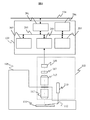
- FIG. 1 is a configuration diagram illustrating an example of a defect observation apparatus of Example 1.
- FIG. FIG. 3 is an internal configuration diagram of an image processing circuit according to the first embodiment.
- FIG. 3 is an explanatory diagram of a detection method using the optical system of Example 1.
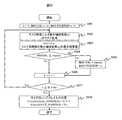
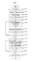
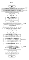
- FIG. 4 is a partially enlarged view of the optical system of FIG. 3. It is a light intensity distribution map in the pupil plane of wafer scattered light. It is a light intensity distribution figure in the pupil plane of the scattered light by a micro foreign material defect. It is a figure which shows the conventional spatial filter for a micro foreign material defect detection. It is a figure which shows an example of the mask image for a minute foreign material defect detection. It is a flowchart of the detection process of the defect position in the optical microscope visual field by one mask image.
- FIG. 1 shows an example of a defect observation apparatus according to an embodiment of the present invention.
- the defect observation apparatus of the present embodiment is applied to an apparatus for observing defects on a wafer generated in a semiconductor device manufacturing process.
- Reference numeral 101 is a wafer which is an object to be inspected.
- Reference numeral 102 denotes an electron microscope (hereinafter referred to as SEM) for observing the wafer 101 in detail.
- Reference numeral 103 denotes an optical microscope that optically detects a defect on the wafer 101 and acquires defect position information thereof.
- Reference numeral 104 denotes a stage on which the wafer 101 can be placed. The stage 104 can move an arbitrary place of the wafer 101 within the field of view of the SEM 102 and the optical microscope 103.
- Reference numeral 105 denotes a vacuum chamber in which the SEM 102, the stage 104, and the objective lens 113 of the optical microscope 103 are housed.
- Reference numeral 110 denotes an illumination light source.
- the laser light emitted from the illumination light source 110 passes through a vacuum-sealed window 111, is reflected by a mirror 112 that controls the illumination position, and is irradiated to an arbitrary position on the surface of the wafer 101.
- Reference numeral 113 denotes an objective lens for collecting scattered light reflected from the sample 101. The light that has passed through the objective lens 113 passes through the vacuum-sealed window 114, is imaged on the microlens array 117 by the imaging lens 115, and is then converted into an electrical signal by the imaging device 116.
- the microlens array 117 is a lens unit in which microlenses are arranged in a lattice shape.
- FIG. 1 shows a configuration in which the objective lens 113 is arranged inside the vacuum chamber 105 and the imaging lens 115 is arranged outside, the scattered light from the sample 101 can be imaged on the microlens array 117, and As long as it does not break the vacuum, it may be an integrated lens that extends over the inside, outside, or both inside and outside of the vacuum chamber 105.
- the control unit 106 includes a stage control circuit 118, an SEM imaging system control circuit 119, an image processing circuit 120, an external input / output I / F 121, a CPU 122, and a memory 123, which are connected to a bus 124 and input information to each other. Output is possible.
- the stage control circuit 118 controls the stage 104
- the SEM imaging system control circuit 119 controls the SEM 102 and stores the detected image signal in the memory 123.
- the image processing circuit 120 performs arithmetic processing on the image data obtained from the image sensor 116 of the optical microscope 103 and detects a defect position in the captured image.
- the external input / output I / F 121 outputs display information to the terminal 107, information input from the terminal 107, information input / output to the storage device 108, a defect inspection device (not shown), a host management system, etc. via the network 109. Input / output information.
- the image data stored in the memory 123 is processed by the CPU 122.
- the optical microscope 103 redetects the position of the defect on the wafer 101 using the defect position information detected by the defect inspection apparatus (not shown) (hereinafter referred to as “defect inspection apparatus”).
- the control unit 106 has a function as position correction means for correcting the position information of the defect based on the position information of the defect detected by the optical microscope 103, and the SEM 102 Based on the defect position information corrected in 106, the defect is observed.
- the stage 104 is configured to be movable so that defects detected by the optical microscope 103 can be observed by the SEM 102.
- FIG. 2 shows details of the image processing circuit 120.
- the image processing circuit 120 includes a data I / F 201, a mask image data storage unit 202, an image information storage unit 203, a calculation unit 204, and a defect classification unit 206, which are connected to an internal bus 205.
- An image obtained by the optical microscope 103 is stored in the image information storage unit 203.
- a mask image is registered in the mask image data storage unit 202 in advance.
- the calculation unit 204 performs calculation processing using the image data stored in the image information storage unit 203 and the mask image stored in the mask image data storage unit 202, and determines a defect position in the image detected by the optical microscope 103. Identify.
- the defect classification unit 206 classifies the defect type based on the selected mask image, as will be described later with reference to FIG.
- the data I / F 201 is connected to the internal bus 205 and the bus 124 in the control unit 106, and exchanges data between the image processing circuit 120 and other processing units in the control unit 106.
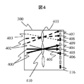
- FIG. 4 is an enlarged view of a portion indicated by 303 in FIG.
- FIG. 3 is a diagram illustrating an optical path of the light beams emitted from the points 300 and 301 on the wafer 101 to the image sensor 116.
- the optical system is divided into an objective lens 113 and an imaging lens 115, and a spatial filter 302 is shown in a pupil region formed between the objective lens 113 and the imaging lens 115.
- the spatial filter 302 shown here is virtual. It is drawn to explain that the action of the microlens array of this configuration has the same effect as a conventional spatial filter.
- the light beam emitted from the point 300 is divided into a light beam indicated by a thick solid line passing through the opening of the spatial filter (corresponding to 400 in FIG. 4) and a light beam indicated by a thin solid line shielded by the spatial filter 302.
- the optical path is indicated by a thin solid line even after being shielded by the spatial filter 302 (corresponding to 401 in FIG. 4).
- the microlens 410 corresponds to the position of the point 300 on the wafer 101 (400 and 401 are optical paths of light emitted from the point 300 on the wafer 101), and light that has passed through the microlens 410 is incident.
- the pixels 404, 405, and 406 of the image sensor correspond to the positions where each light beam has passed through the imaging lens 115.
- the light rays are parallel, so that the pixels 404, 405, and 406 correspond to the spatial position of the pupil plane. That is, in the example of the spatial filter 302 in FIG.
- the opening portion of the spatial filter corresponds to the pixels 404 and 405, and the shielding portion corresponds to the pixel 406. From this, even if the spatial filter 302 is not placed, if a process for invalidating a pixel to which a light ray conventionally shielded by the spatial filter 302 is incident after being received by the image sensor 116, a minute region corresponding to the microlens 410 is obtained. Thus, an effect equivalent to that of the spatial filter 302 can be obtained.
- the valid pixels 404 and 405 are indicated by white squares
- the invalid pixels 406 are indicated by black squares.
- the microlens array 117 and the image sensor 116 are shown one-dimensionally. Actually, however, the microlens array 117 has a microlens spread in a lattice shape, and the image sensor 116 is an area. It is a sensor. The portion indicated by three pixels in one row corresponding to the microlens 410 in FIG. 4 may be configured by the number of planar pixels that can practically express the spatial filter shape for each type of defect. Similarly, the microlens 411 and the pixels 407, 408, and 409 of the image sensor correspond to the point 301 on the wafer 101.
- the entire field of view on the wafer can be detected with N ⁇ N resolution, and the spatial filter can be detected with M ⁇ M resolution.
- the microlens array is configured by N ⁇ N, and the field of view of one microlens is imaged with M ⁇ M pixels.
- FIG. 21A of Patent Document 1 discloses the intensity distribution of the radially polarized (P-polarized) component and the azimuth-polarized (S-polarized) component of the scattered light from the wafer surface calculated using the scattered light simulation. ing.
- FIG. 5 is a total of the intensities of both, and is a simulation diagram of the light intensity distribution observed by the scattered light from the wafer. The higher the scattered light intensity, the more white it is drawn.
- FIG. 21B of Patent Document 1 discloses the intensity distribution of the radially polarized (P-polarized) component and the azimuth-polarized (S-polarized) component of the scattered light from a spherical foreign substance having a diameter of 18 nm.
- FIG. 6 is a summation of both intensities, and is a simulated diagram of a light intensity distribution observed by scattered light of a spherical foreign substance having a diameter of 18 nm. Like FIG. 5, the stronger the scattered light intensity, the more white it is drawn.
- FIG. 7 shows one of the light shielding plates of the spatial filter disclosed in FIG. 34 of Patent Document 1.
- the black part is the shielding part and the white part is the opening part. 7 and the light intensity distributions in FIGS. 5 and 6 are compared, most of the scattered light from the wafer in FIG. 5 is shielded by a spatial filter, and the scattered light from the spherical foreign material in FIG. The right half passes through the opening.
- most of the scattered light after passing through the spatial filter is from the spherical foreign matter, and the scattered light of the foreign matter can be extracted with high sensitivity from the scattered light from the foreign matter on the wafer.
- FIGS. 5 and 6 are observed in the cross section of the space between the objective lens 113 and the imaging lens 115 in FIG. 3, but when a spherical foreign substance having a diameter of 18 nm is present at a point 300 in FIG. Then, the light intensity distributions shown in FIGS. 5 and 6 are generated on the image sensor corresponding to the microlens 410 shown in FIG. 4, and as a result, a light intensity distribution image corresponding to the target minute region can be obtained. .
- FIG. 8 is an image of the spatial filter of FIG. 7 with M ⁇ M resolution. This is a mask image, which is stored in the mask image data storage unit 202 of FIG.
- the pixel values shown in FIG. 8 are 0 for black and 1 for white. Since the image observed in the spatial section between the objective lens 113 and the imaging lens 115 is inverted vertically and horizontally on the image sensor, it is actually inverted vertically and horizontally in FIG.
- Mask processing is applied to the light intensity distribution image of the target minute region obtained through the microlens 410 shown in FIG. That is, the pixel corresponding to the black pixel in FIG. 8 in the minute region light intensity distribution image (hereinafter, minute region image) is set to 0, and the pixel corresponding to the white pixel retains the original pixel value (S902). Thereby, the effect similar to the shielding of the light by the conventional spatial filter can be acquired.
- the same process is performed on the minute area images corresponding to all the N ⁇ N microlenses, and the maximum brightness or the average maximum brightness including neighboring pixels is selected from the processed N ⁇ N minute area images.
- a micro-region image is selected (S905). Since the detection visual field of the present optical system is determined by an N ⁇ N microlens array, the position of the defect in the detection visual field can be specified by the position of the microlens corresponding to the minute region image having the maximum luminance (S908). ). However, round () in S908 represents the integer part of the result of division, and mod () represents the number of remainders.
- FIG. 10 shows an example of how to assign the microlens numbers and X and Y coordinates of the microlens array.
- MAX_POSITION N + 2
- the obtained X and Y may be multiplied by the pixel pitch and the imaging magnification.
- the defect coordinate position in the optical system visual field can be converted into the coordinates of the stage 104 and detected by the optical microscope 103. From the defect position, the defect can be located at the center of the field of view of the SEM 102.
- ⁇ Intensity distribution of scattered light varies depending not only on the type of defect but also the direction of the defect. Therefore, if a plurality of mask images are prepared corresponding to the direction of the defect, this can be dealt with. According to the method of the present invention, this can be realized by preparing in advance mask images for a plurality of types of defects and the directions of the plurality of defects, and performing mask processing on the detected minute region light intensity distribution image.
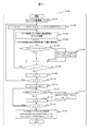
- Steps S1102 to S1108 are processing for the mask image (r), which is the same as that described in FIG. While recording the maximum luminance values MAX_VAL (r) and MAX_POSITION (r) (S1106), the process is repeated until all the masks are processed (S1110). When all mask processes are completed, the image number (max_r) having the maximum luminance is detected in steps S1111 to S1115 (S1113).
- the defect position in the detection visual field is specified from max_r (S1116).
- the method for specifying the defect position is the same as that described with reference to FIG.
- the maximum luminance value MAX_VAL (r) is recorded.
- the maximum luminance value to be recorded is normalized by the area of 1 of the mask image (the portion corresponding to the opening of the spatial filter), and the defect type.
- MAX_VAL (r) may be obtained by multiplying a predetermined coefficient every time, or the maximum luminance value obtained after normalizing the luminance value of the image after mask processing.
- the two detected by the SEM are used so that the property of the defect corresponding to the mask image number max_r for detecting the defect position, for example, the property such as unevenness, becomes obvious in the observation image of the SEM.
- an observation image is generated using a secondary electron image and a reflected electron image, it is possible to change image capturing conditions such as a mixing ratio of each image for each defect.
- FIG. 12 illustrates a procedure for correcting defect coordinates using the present optical system and collecting an SEM defect image with the SEM shown in FIG. 1, with reference to FIGS.
- the wafer 101 to be observed is loaded on the stage 104 (S1201).
- the defect coordinate data of the defect detected in advance by the inspection apparatus is read into the memory 123 via the external input / output I / F 121 of the overall control unit 106 (S1202). Select (S1203).
- the defect may be selected by the CPU 122 by a preset program, or may be selected by the operator via the terminal 107.
- wafer alignment is performed (S1204).
- the wafer coordinates and the stage coordinates are associated with each other using positioning marks (alignment marks) whose coordinates on the wafer are known. The result of this association is stored in the memory 123 as alignment information.
- defect positions are corrected for defects 1 to M selected as observation targets.
- the defect m is moved to the field of view of the optical microscope 103 (S1206).
- the CPU 122 calculates the stage coordinates corresponding to the defect m from the defect coordinate data stored in the memory 123 and the alignment information, thereby driving the stage 104 via the stage control circuit 118. Done.
- the position of the defect m is specified by the process shown in FIG. 11 (S1100), and the specified position of the defect is stored as the corrected defect position m (S1207).
- the image of the defect m imaged by the optical microscope 103 is stored in the image information storage unit 203, and the image of the defect m and the mask image stored in the mask image data storage unit 202 are calculated.
- the data is read by the unit 204, and the masking process and the process shown in S1100 of FIG.
- Some inspection apparatuses output not only the detected defect position coordinates but also information on defect characteristics. For example, if the defect feature information indicates in advance whether the defect is convex or concave, the mask image to be used may be changed for each defect and used.
- information for specifying the use mask image corresponding to the defect feature information is stored in the memory 123 in advance as a table. Then, when the defect coordinate data of the defect detected by the inspection apparatus described above is read into the memory 123, the defect feature information is also read.
- the mask image specifying information to be used is read with reference to the table information stored in the memory 123, and the mask to be used when executing the processing S1100 from the mask image data storage unit 202. What is necessary is just to read an image.
- the corrected defect positions m are read from the memory 123, and the position information is converted into stage coordinates as necessary.
- the defect m is sequentially moved to the field of view of the SEM 102 by giving to the stage control circuit 118 (S1211), and an SEM image of the defect m is captured (S1212, S1213, S1214). After taking SEM images of all defects, the wafer is unloaded (S1215), and the process is terminated.
- the mask image is determined by the type and direction of the defect. From the mask image used for detecting the defect position, the type and direction of the defect can be known before SEM imaging. As a result, it is possible to set an optimum imaging condition in which the defect is easy to see according to the type and direction of the defect. Further, since the type and direction of the defect can be known from the mask image used for detecting the defect position, it can be used for defect classification information.
- FIG. 13 shows an example of an overall flowchart of the defect observation apparatus according to the second embodiment of the present invention.
- information on the mask image used for defect detection is used to control the SEM imaging conditions and classify the defect images captured by the SEM.
- the configuration of the defect observation apparatus is as shown in FIGS. 1 and 2, and in particular, the defect classification unit 206 is provided in the image processing circuit 120 of FIG.
- a correspondence table between mask image numbers and SEM imaging conditions is created using the terminal 107 or an external input device (S1301) and stored in the memory 123.
- a table of mask image numbers and defect types is created (S1302) and stored in the memory 123.
- S1301 and S1302 do not necessarily have to be performed for each wafer, and the mask image number and the SEM imaging condition or the mask image number and the defect type have a fixed relationship as in each semiconductor device product to be observed or each manufacturing process. Create it for each condition.
- a defect image is taken by SEM in S1211, S1212.
- the mask image number and SEM imaging condition table stored in the memory 123 and the mask image number m corresponding to the imaging defect are referred to, and the SEM imaging condition is changed via the SEM imaging control circuit 119.
- the change in the SEM imaging condition may be a change in the image mixture ratio when generating an observation image from a plurality of captured images.
- the mask image number and defect type table stored in the memory 123 and the mask image number m corresponding to the imaging defect are referred to, the defect m classification information is stored in the memory 123 and used as defect classification information.
- S1305 may be executed after S1100 of the defect position detection process by the optical microscope.
- optical detection system described above By mounting the optical detection system described above in the SEM defect observation apparatus, it becomes possible to detect the defect position with high sensitivity and high speed for a plurality of types of defects detected by the inspection apparatus.
- optically different detection has been performed by changing the spatial filter.
- this is realized by image processing. Therefore, optical imaging only needs to be performed once per defect, and throughput due to imaging time is also reduced. Does not occur.
- SEM observation at the defect detection position by optical detection it becomes possible to reliably put the defect in the observation field of SEM, and the success rate of automatic imaging of the SEM observation image of the defect detected by the inspection apparatus is improved. , The throughput of defect automatic imaging in SEM is also improved.
- the pupil space between the lenses which has been conventionally required for installing the spatial filter, becomes unnecessary, so that the optical microscope can be downsized.
Landscapes
- General Physics & Mathematics (AREA)
- Physics & Mathematics (AREA)
- Chemical & Material Sciences (AREA)
- Life Sciences & Earth Sciences (AREA)
- Pathology (AREA)
- Analytical Chemistry (AREA)
- Biochemistry (AREA)
- General Health & Medical Sciences (AREA)
- Health & Medical Sciences (AREA)
- Immunology (AREA)
- Engineering & Computer Science (AREA)
- Computer Vision & Pattern Recognition (AREA)
- Theoretical Computer Science (AREA)
- Signal Processing (AREA)
- Quality & Reliability (AREA)
- Crystallography & Structural Chemistry (AREA)
- Investigating Materials By The Use Of Optical Means Adapted For Particular Applications (AREA)
- Testing Or Measuring Of Semiconductors Or The Like (AREA)
Abstract
Description
Claims (13)
- 被検査物に光を照射する照射系と、
光の照射により発生した散乱光を結像する光学系と、
前記光学系の結像面に配置されたマイクロレンズアレイと、
前記光学系の結像面からずらした位置に配置され、前記マイクロレンズアレイを通過した光を撮像する撮像素子と、
欠陥種類ごとに、あるいは欠陥の方向ごとに生成した複数のマスク画像を記憶するマスク画像記憶部と、
前記撮像素子より得られた画像に、前記複数のマスク画像でマスク処理を実行し、欠陥検出処理を行う演算部と、
を有する欠陥検出装置。 - 請求項1に記載の欠陥検出装置において、
前記マスク画像は、半導体ウェーハからの散乱光と、欠陥からの散乱光を区別するものである欠陥検出装置。 - 請求項1に記載の欠陥検出装置において、
前記演算部は、複数のマスク画像でマスク処理を実行して得られた画像の内、高輝度の画像から欠陥位置を検出する欠陥検出装置。 - 請求項1に記載の欠陥検出装置において、
欠陥検出処理で選択されたマスク画像に基づいて、欠陥種類を分類する欠陥分類部を有する欠陥検出装置。 - 被検査物に光を照射する照射系と、光の照射により発生した散乱光を結像する光学系と、前記光学系の結像面に配置されたマイクロレンズアレイと、前記光学系の結像面からずらした位置に配置され、前記マイクロレンズアレイを通過した光を撮像する撮像素子とを用いる欠陥検出方法であって、
欠陥種類ごとに、あるいは欠陥の方向ごとに生成された複数のマスク画像を記憶するステップと、
前記撮像素子より得られた画像に、前記複数のマスク画像によりマスク処理を行うステップと、
マスク処理を行った画像により欠陥検出を行うステップと
を有する欠陥検出方法。 - 請求項5に記載の欠陥検出方法において、
前記マスク画像は、半導体ウェーハからの散乱光と、欠陥からの散乱光を区別するものである欠陥検出方法。 - 請求項5に記載の欠陥検出方法において、
前記欠陥検出を行うステップは、複数のマスク画像でマスク処理を実行して得られた画像の内、高輝度の画像から欠陥位置を検出する欠陥検出方法。 - 請求項5に記載の欠陥検出方法において、更に、
欠陥検出処理で選択されたマスク画像に基づいて欠陥種類を分類するステップを有する欠陥検出方法。 - SEMと光学顕微鏡と画像処理部とを備える欠陥観察装置であって、
前記光学顕微鏡は、試料に光を照射する照射系と、光の照射により発生した散乱光を結像する光学系と、前記光学系の結像面に配置したマイクロレンズアレイと、前記光学系の結像面からずらした位置に配置され、前記マイクロレンズアレイを通過した光を撮像する撮像素子とを備え、
前記画像処理部は、欠陥の種類ごとに、あるいは欠陥の方向ごとに生成した複数のマスク画像を記憶するマスク画像記憶部と、前記撮像素子で撮像した撮像画像を記憶する画像記憶部と、前記マスク画像と前記撮像画像を用いて試料の欠陥位置を算出する演算部を備える欠陥観察装置。 - 請求項9に記載の欠陥観察装置において、
前記マスク画像は、半導体ウェーハからの散乱光と、欠陥からの散乱光を区別するものである欠陥観察装置。 - 請求項9に記載の欠陥観察装置において、
前記演算部は、複数のマスク画像でマスク処理を実行して得られた画像の内、高輝度の画像から欠陥位置を算出する欠陥観察装置。 - 請求項9に記載の欠陥観察装置において、
欠陥位置を算出のために使用されたマスク画像により、SEMで得た二次電子像、反射電子像など性質の異なる画像の混合比を変更して観察画像を生成する欠陥観察装置。 - 請求項9に記載の欠陥観察装置において、更に、
欠陥検出処理で選択されたマスク画像に基づいて、欠陥種類を分類する欠陥分類部を備える欠陥観察装置。
Priority Applications (4)
| Application Number | Priority Date | Filing Date | Title |
|---|---|---|---|
| KR1020207018676A KR102345254B1 (ko) | 2018-02-27 | 2018-02-27 | 결함 검출 장치, 결함 검출 방법 및 결함 관찰 장치 |
| JP2020503132A JP6920009B2 (ja) | 2018-02-27 | 2018-02-27 | 欠陥検出装置、欠陥検出方法および欠陥観察装置 |
| PCT/JP2018/007297 WO2019167129A1 (ja) | 2018-02-27 | 2018-02-27 | 欠陥検出装置、欠陥検出方法および欠陥観察装置 |
| US16/970,451 US11802841B2 (en) | 2018-02-27 | 2018-02-27 | Defect detection device, defect detection method, and defect observation device |
Applications Claiming Priority (1)
| Application Number | Priority Date | Filing Date | Title |
|---|---|---|---|
| PCT/JP2018/007297 WO2019167129A1 (ja) | 2018-02-27 | 2018-02-27 | 欠陥検出装置、欠陥検出方法および欠陥観察装置 |
Publications (1)
| Publication Number | Publication Date |
|---|---|
| WO2019167129A1 true WO2019167129A1 (ja) | 2019-09-06 |
Family
ID=67805298
Family Applications (1)
| Application Number | Title | Priority Date | Filing Date |
|---|---|---|---|
| PCT/JP2018/007297 Ceased WO2019167129A1 (ja) | 2018-02-27 | 2018-02-27 | 欠陥検出装置、欠陥検出方法および欠陥観察装置 |
Country Status (4)
| Country | Link |
|---|---|
| US (1) | US11802841B2 (ja) |
| JP (1) | JP6920009B2 (ja) |
| KR (1) | KR102345254B1 (ja) |
| WO (1) | WO2019167129A1 (ja) |
Cited By (1)
| Publication number | Priority date | Publication date | Assignee | Title |
|---|---|---|---|---|
| WO2024053109A1 (ja) * | 2022-09-09 | 2024-03-14 | 日本電信電話株式会社 | 劣化検出モデル学習装置、劣化検出装置、及びプログラム |
Families Citing this family (3)
| Publication number | Priority date | Publication date | Assignee | Title |
|---|---|---|---|---|
| CN112730334B (zh) * | 2020-12-23 | 2024-03-22 | 之江实验室 | 基于电偶极旋转散射光探测的纳米微粒识别装置和方法 |
| JP7654463B2 (ja) * | 2021-05-19 | 2025-04-01 | キヤノン株式会社 | 情報処理装置、情報処理方法、およびプログラム |
| CN117058004B (zh) * | 2023-10-13 | 2024-03-08 | 埃克斯工业有限公司 | 晶圆的晶粒图像重构方法、电子设备及存储介质 |
Citations (6)
| Publication number | Priority date | Publication date | Assignee | Title |
|---|---|---|---|---|
| JPS5780546A (en) * | 1980-11-07 | 1982-05-20 | Nippon Kogaku Kk <Nikon> | Detecting device for foreign substance |
| JP2005535869A (ja) * | 2002-01-15 | 2005-11-24 | アプライド マテリアルズ インコーポレイテッド | 空間フィルタリングを使用したパターン化されたウェハの検査 |
| JP2011106974A (ja) * | 2009-11-18 | 2011-06-02 | Hitachi High-Technologies Corp | 欠陥検出方法及び欠陥検出装置並びにこれを備えた欠陥観察装置 |
| JP2011226989A (ja) * | 2010-04-22 | 2011-11-10 | Kobe Steel Ltd | 表面形状測定装置および半導体ウェハ検査装置 |
| JP2012185149A (ja) * | 2011-02-17 | 2012-09-27 | Ricoh Co Ltd | 欠陥検査装置及び欠陥検査処理方法 |
| US20170219487A1 (en) * | 2016-02-02 | 2017-08-03 | Kla-Tencor Corporation | System and Method for Hyperspectral Imaging Metrology |
Family Cites Families (7)
| Publication number | Priority date | Publication date | Assignee | Title |
|---|---|---|---|---|
| US5659390A (en) * | 1995-02-09 | 1997-08-19 | Inspex, Inc. | Method and apparatus for detecting particles on a surface of a semiconductor wafer having repetitive patterns |
| WO2006039486A2 (en) | 2004-10-01 | 2006-04-13 | The Board Of Trustees Of The Leland Stanford Junior University | Imaging arrangements and methods therefor |
| JP5416600B2 (ja) * | 2010-01-22 | 2014-02-12 | 株式会社日立ハイテクノロジーズ | 欠陥検査装置およびその方法 |
| JP5629782B2 (ja) * | 2010-12-27 | 2014-11-26 | 株式会社日立ハイテクノロジーズ | 検査装置 |
| JP5882072B2 (ja) * | 2012-02-06 | 2016-03-09 | 株式会社日立ハイテクノロジーズ | 欠陥観察方法及びその装置 |
| JP2015059776A (ja) * | 2013-09-18 | 2015-03-30 | 株式会社日立ハイテクノロジーズ | 欠陥観察装置およびその方法 |
| JP6401648B2 (ja) | 2015-03-31 | 2018-10-10 | 株式会社Screenホールディングス | 欠陥分類装置および欠陥分類方法 |
-
2018
- 2018-02-27 KR KR1020207018676A patent/KR102345254B1/ko active Active
- 2018-02-27 JP JP2020503132A patent/JP6920009B2/ja active Active
- 2018-02-27 WO PCT/JP2018/007297 patent/WO2019167129A1/ja not_active Ceased
- 2018-02-27 US US16/970,451 patent/US11802841B2/en active Active
Patent Citations (6)
| Publication number | Priority date | Publication date | Assignee | Title |
|---|---|---|---|---|
| JPS5780546A (en) * | 1980-11-07 | 1982-05-20 | Nippon Kogaku Kk <Nikon> | Detecting device for foreign substance |
| JP2005535869A (ja) * | 2002-01-15 | 2005-11-24 | アプライド マテリアルズ インコーポレイテッド | 空間フィルタリングを使用したパターン化されたウェハの検査 |
| JP2011106974A (ja) * | 2009-11-18 | 2011-06-02 | Hitachi High-Technologies Corp | 欠陥検出方法及び欠陥検出装置並びにこれを備えた欠陥観察装置 |
| JP2011226989A (ja) * | 2010-04-22 | 2011-11-10 | Kobe Steel Ltd | 表面形状測定装置および半導体ウェハ検査装置 |
| JP2012185149A (ja) * | 2011-02-17 | 2012-09-27 | Ricoh Co Ltd | 欠陥検査装置及び欠陥検査処理方法 |
| US20170219487A1 (en) * | 2016-02-02 | 2017-08-03 | Kla-Tencor Corporation | System and Method for Hyperspectral Imaging Metrology |
Cited By (3)
| Publication number | Priority date | Publication date | Assignee | Title |
|---|---|---|---|---|
| WO2024053109A1 (ja) * | 2022-09-09 | 2024-03-14 | 日本電信電話株式会社 | 劣化検出モデル学習装置、劣化検出装置、及びプログラム |
| JPWO2024053109A1 (ja) * | 2022-09-09 | 2024-03-14 | ||
| JP7820670B2 (ja) | 2022-09-09 | 2026-02-26 | Ntt株式会社 | 劣化検出モデル学習装置、劣化検出装置、及びプログラム |
Also Published As
| Publication number | Publication date |
|---|---|
| US20210109035A1 (en) | 2021-04-15 |
| KR102345254B1 (ko) | 2021-12-31 |
| JP6920009B2 (ja) | 2021-08-18 |
| US11802841B2 (en) | 2023-10-31 |
| KR20200092372A (ko) | 2020-08-03 |
| JPWO2019167129A1 (ja) | 2020-12-17 |
Similar Documents
| Publication | Publication Date | Title |
|---|---|---|
| JP4009409B2 (ja) | パターン欠陥検査方法及びその装置 | |
| TWI558997B (zh) | 缺陷觀察方法及其裝置 | |
| US6630996B2 (en) | Optical method and apparatus for inspecting large area planar objects | |
| US7355691B2 (en) | Defect inspection apparatus and defect inspection method | |
| TWI741515B (zh) | 缺陷檢測裝置、缺陷檢測方法以及具備其之缺陷觀察裝置 | |
| US20040012775A1 (en) | Optical method and apparatus for inspecting large area planar objects | |
| JP6364193B2 (ja) | 焦点位置調整方法および検査方法 | |
| JP6640482B2 (ja) | パターン検査装置及びパターン検査方法 | |
| JP2002014057A (ja) | 欠陥検査装置 | |
| KR101994524B1 (ko) | 포커싱 장치, 포커싱 방법 및 패턴 검사 방법 | |
| JP6920009B2 (ja) | 欠陥検出装置、欠陥検出方法および欠陥観察装置 | |
| JP2012251785A (ja) | 検査装置および検査方法 | |
| JP4939843B2 (ja) | 欠陥検査方法及びその装置 | |
| JP2020042035A (ja) | パターン検査装置及びパターン検査方法 | |
| TWI862849B (zh) | 藉由組合來自多個收集通道之資訊之設計至晶圓影像相關性 | |
| TWI885268B (zh) | 處理半導體晶圓影像的系統及方法 | |
| JP6220553B2 (ja) | 焦点位置調整方法および検査方法 | |
| JP2009058382A (ja) | 多重スキャンによる画像取得方法、画像取得装置および試料検査装置 | |
| JP2005077272A (ja) | 欠陥検査方法 | |
| JPH0682373A (ja) | 欠陥検査方法 | |
| JP3803677B2 (ja) | 欠陥分類装置及び欠陥分類方法 | |
| JP2002333406A (ja) | 外観検査装置および外観検査方法 | |
| JPH04165641A (ja) | ウェーハ外観検査装置 | |
| CN114943677A (zh) | 缺陷检测方法以及利用其的半导体装置的制造方法 | |
| CN121739882A (zh) | 确定空间滤波器的布设位置的方法、光学系统及检测设备 |
Legal Events
| Date | Code | Title | Description |
|---|---|---|---|
| 121 | Ep: the epo has been informed by wipo that ep was designated in this application |
Ref document number: 18907674 Country of ref document: EP Kind code of ref document: A1 |
|
| ENP | Entry into the national phase |
Ref document number: 2020503132 Country of ref document: JP Kind code of ref document: A |
|
| ENP | Entry into the national phase |
Ref document number: 20207018676 Country of ref document: KR Kind code of ref document: A |
|
| NENP | Non-entry into the national phase |
Ref country code: DE |
|
| 122 | Ep: pct application non-entry in european phase |
Ref document number: 18907674 Country of ref document: EP Kind code of ref document: A1 |