WO2019167102A1 - 半導体装置及び半導体装置の製造方法 - Google Patents
半導体装置及び半導体装置の製造方法 Download PDFInfo
- Publication number
- WO2019167102A1 WO2019167102A1 PCT/JP2018/007089 JP2018007089W WO2019167102A1 WO 2019167102 A1 WO2019167102 A1 WO 2019167102A1 JP 2018007089 W JP2018007089 W JP 2018007089W WO 2019167102 A1 WO2019167102 A1 WO 2019167102A1
- Authority
- WO
- WIPO (PCT)
- Prior art keywords
- semiconductor device
- semiconductor chip
- electrode
- solder material
- solder
- Prior art date
- Legal status (The legal status is an assumption and is not a legal conclusion. Google has not performed a legal analysis and makes no representation as to the accuracy of the status listed.)
- Ceased
Links
Images





Classifications
-
- H—ELECTRICITY
- H10—SEMICONDUCTOR DEVICES; ELECTRIC SOLID-STATE DEVICES NOT OTHERWISE PROVIDED FOR
- H10W—GENERIC PACKAGES, INTERCONNECTIONS, CONNECTORS OR OTHER CONSTRUCTIONAL DETAILS OF DEVICES COVERED BY CLASS H10
- H10W72/00—Interconnections or connectors in packages
-
- H—ELECTRICITY
- H10—SEMICONDUCTOR DEVICES; ELECTRIC SOLID-STATE DEVICES NOT OTHERWISE PROVIDED FOR
- H10W—GENERIC PACKAGES, INTERCONNECTIONS, CONNECTORS OR OTHER CONSTRUCTIONAL DETAILS OF DEVICES COVERED BY CLASS H10
- H10W72/00—Interconnections or connectors in packages
- H10W72/071—Connecting or disconnecting
- H10W72/073—Connecting or disconnecting of die-attach connectors
-
- H—ELECTRICITY
- H10—SEMICONDUCTOR DEVICES; ELECTRIC SOLID-STATE DEVICES NOT OTHERWISE PROVIDED FOR
- H10W—GENERIC PACKAGES, INTERCONNECTIONS, CONNECTORS OR OTHER CONSTRUCTIONAL DETAILS OF DEVICES COVERED BY CLASS H10
- H10W72/00—Interconnections or connectors in packages
- H10W72/071—Connecting or disconnecting
- H10W72/073—Connecting or disconnecting of die-attach connectors
- H10W72/07351—Connecting or disconnecting of die-attach connectors characterised by changes in properties of the die-attach connectors during connecting
- H10W72/07354—Connecting or disconnecting of die-attach connectors characterised by changes in properties of the die-attach connectors during connecting changes in dispositions
-
- H—ELECTRICITY
- H10—SEMICONDUCTOR DEVICES; ELECTRIC SOLID-STATE DEVICES NOT OTHERWISE PROVIDED FOR
- H10W—GENERIC PACKAGES, INTERCONNECTIONS, CONNECTORS OR OTHER CONSTRUCTIONAL DETAILS OF DEVICES COVERED BY CLASS H10
- H10W72/00—Interconnections or connectors in packages
- H10W72/071—Connecting or disconnecting
- H10W72/075—Connecting or disconnecting of bond wires
-
- H—ELECTRICITY
- H10—SEMICONDUCTOR DEVICES; ELECTRIC SOLID-STATE DEVICES NOT OTHERWISE PROVIDED FOR
- H10W—GENERIC PACKAGES, INTERCONNECTIONS, CONNECTORS OR OTHER CONSTRUCTIONAL DETAILS OF DEVICES COVERED BY CLASS H10
- H10W72/00—Interconnections or connectors in packages
- H10W72/30—Die-attach connectors
- H10W72/341—Dispositions of die-attach connectors, e.g. layouts
- H10W72/347—Dispositions of multiple die-attach connectors
-
- H—ELECTRICITY
- H10—SEMICONDUCTOR DEVICES; ELECTRIC SOLID-STATE DEVICES NOT OTHERWISE PROVIDED FOR
- H10W—GENERIC PACKAGES, INTERCONNECTIONS, CONNECTORS OR OTHER CONSTRUCTIONAL DETAILS OF DEVICES COVERED BY CLASS H10
- H10W72/00—Interconnections or connectors in packages
- H10W72/851—Dispositions of multiple connectors or interconnections
- H10W72/853—On the same surface
- H10W72/871—Bond wires and strap connectors
-
- H—ELECTRICITY
- H10—SEMICONDUCTOR DEVICES; ELECTRIC SOLID-STATE DEVICES NOT OTHERWISE PROVIDED FOR
- H10W—GENERIC PACKAGES, INTERCONNECTIONS, CONNECTORS OR OTHER CONSTRUCTIONAL DETAILS OF DEVICES COVERED BY CLASS H10
- H10W72/00—Interconnections or connectors in packages
- H10W72/851—Dispositions of multiple connectors or interconnections
- H10W72/874—On different surfaces
- H10W72/884—Die-attach connectors and bond wires
-
- H—ELECTRICITY
- H10—SEMICONDUCTOR DEVICES; ELECTRIC SOLID-STATE DEVICES NOT OTHERWISE PROVIDED FOR
- H10W—GENERIC PACKAGES, INTERCONNECTIONS, CONNECTORS OR OTHER CONSTRUCTIONAL DETAILS OF DEVICES COVERED BY CLASS H10
- H10W72/00—Interconnections or connectors in packages
- H10W72/90—Bond pads, in general
- H10W72/921—Structures or relative sizes of bond pads
- H10W72/926—Multiple bond pads having different sizes
-
- H—ELECTRICITY
- H10—SEMICONDUCTOR DEVICES; ELECTRIC SOLID-STATE DEVICES NOT OTHERWISE PROVIDED FOR
- H10W—GENERIC PACKAGES, INTERCONNECTIONS, CONNECTORS OR OTHER CONSTRUCTIONAL DETAILS OF DEVICES COVERED BY CLASS H10
- H10W72/00—Interconnections or connectors in packages
- H10W72/90—Bond pads, in general
- H10W72/941—Dispositions of bond pads
- H10W72/944—Dispositions of multiple bond pads
-
- H—ELECTRICITY
- H10—SEMICONDUCTOR DEVICES; ELECTRIC SOLID-STATE DEVICES NOT OTHERWISE PROVIDED FOR
- H10W—GENERIC PACKAGES, INTERCONNECTIONS, CONNECTORS OR OTHER CONSTRUCTIONAL DETAILS OF DEVICES COVERED BY CLASS H10
- H10W74/00—Encapsulations, e.g. protective coatings
-
- H—ELECTRICITY
- H10—SEMICONDUCTOR DEVICES; ELECTRIC SOLID-STATE DEVICES NOT OTHERWISE PROVIDED FOR
- H10W—GENERIC PACKAGES, INTERCONNECTIONS, CONNECTORS OR OTHER CONSTRUCTIONAL DETAILS OF DEVICES COVERED BY CLASS H10
- H10W90/00—Package configurations
- H10W90/701—Package configurations characterised by the relative positions of pads or connectors relative to package parts
- H10W90/751—Package configurations characterised by the relative positions of pads or connectors relative to package parts of bond wires
- H10W90/756—Package configurations characterised by the relative positions of pads or connectors relative to package parts of bond wires between a chip and a stacked lead frame, conducting package substrate or heat sink
-
- H—ELECTRICITY
- H10—SEMICONDUCTOR DEVICES; ELECTRIC SOLID-STATE DEVICES NOT OTHERWISE PROVIDED FOR
- H10W—GENERIC PACKAGES, INTERCONNECTIONS, CONNECTORS OR OTHER CONSTRUCTIONAL DETAILS OF DEVICES COVERED BY CLASS H10
- H10W90/00—Package configurations
- H10W90/701—Package configurations characterised by the relative positions of pads or connectors relative to package parts
- H10W90/761—Package configurations characterised by the relative positions of pads or connectors relative to package parts of strap connectors
- H10W90/766—Package configurations characterised by the relative positions of pads or connectors relative to package parts of strap connectors between a chip and a stacked lead frame, conducting package substrate or heat sink
Definitions
- the present invention relates to a semiconductor device and a method for manufacturing the semiconductor device.
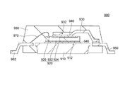
- a conventional semiconductor device 900 described in Patent Document 1 is arranged on a substrate 910 having a semiconductor chip arrangement surface 912 and a semiconductor chip arrangement surface 912, and a surface on the substrate 910 side (semiconductor chip arrangement).
- the collector electrode 922 formed on the surface facing the surface 12
- the emitter formed on the surface opposite to the surface on the substrate 910 side (the surface opposite to the surface facing the semiconductor chip placement surface 12).
- a semiconductor chip 920 having a gate electrode 926 formed at a position separated from the electrode 924 (electrode) and the emitter electrode 924, and an electrode connection piece 932, and the electrode connection piece 932 via the emitter electrode 924 and the solder 940 A joined lead 930;
- the electrode connection piece 932 is joined to the emitter electrode 924 via the solder 940, that is, the semiconductor chip 920 and the lead 930 are connected only via the solder 940 (interposition member such as a wire). Therefore, the semiconductor device 900 has a large current capacity and is suitable for an electronic device (for example, a power source) that uses a large current.
- the paste-like solder material 941 has a certain thickness or more, the solder material 941 is crushed when the lead 930 is disposed on the solder material 941, and an excess solder material is formed. There is a possibility that it may protrude to an undesired place and the reliability of the semiconductor device may be reduced (see FIG. 13).
- the present invention has been made to solve the above-described problems, and an object of the present invention is to provide a semiconductor device whose reliability is hardly lowered. Moreover, it aims at providing the manufacturing method of the semiconductor device for manufacturing such a semiconductor device.
- a semiconductor device includes a substrate having a semiconductor chip arrangement surface, and an electrode formed on the surface opposite to the surface opposite to the semiconductor chip arrangement surface, disposed on the semiconductor chip arrangement surface.
- the lead has a shape bent toward the semiconductor chip at the convex portion when viewed in cross section.
- a side surface shape of the convex portion is a taper shape narrow on the semiconductor chip side.
- a side shape of the convex portion is a rounded shape.
- the thickness of the solder is preferably 300 ⁇ m or more.
- a first method for manufacturing a semiconductor device is a method for manufacturing a semiconductor device according to any one of [1] to [5], wherein a semiconductor is formed on a substrate.
- Semiconductor chip placement step of placing a chip, a protruding portion protruding to one surface side, and formed on the top of the protruding portion, penetrating from the one surface to the other surface opposite to the one surface
- a lead having an electrode connection piece having a through-hole formed in a state in which the electrode of the semiconductor chip and the electrode connection piece are opposed to each other with a solder material interposed therebetween, and the convex portion protrudes toward the electrode side.
- a second method for manufacturing a semiconductor device according to the present invention is a method for manufacturing a semiconductor device according to any one of [1] to [5], wherein the semiconductor is formed on a substrate.
- Semiconductor chip placement step of placing a chip, a protruding portion protruding to one surface side, and formed on the top of the protruding portion, penetrating from the one surface to the other surface opposite to the one surface
- a lead having a solder material disposed in a predetermined region including the through hole on the other surface, and an electrode of the semiconductor chip and the electrode connection piece.
- solder material is disposed also in a part between the electrode and the electrode connection piece in the assembly forming step.
- the lead having a shape bent toward the semiconductor chip at the convex portion when viewed in cross section is disposed. Is preferred.
- the lead having a tapered shape in which a side surface shape of the convex portion is narrow on the semiconductor chip side is disposed.
- the lead having a rounded shape on the side surface of the convex portion is disposed.
- the solder material is preferably made of a paste-like solder material containing a solvent.
- the electrode connection piece is formed on the semiconductor chip side in the region to be joined with the solder, and is formed on the top of the convex portion, and from the surface on the semiconductor chip side to the semiconductor chip side.
- Has a through-hole penetrating to the opposite surface so that when the lead is placed on the solder material in the manufacturing process, excess solder material passes through the through-hole to the opposite surface of the lead from the semiconductor chip. Can be made to flow. Therefore, in the case where the thickness of the solder is maintained at a certain level or more, even when the lead is arranged on the solder material (before the joining process), it is possible to prevent the excessive solder material from protruding to an undesired place. Therefore, the reliability of the semiconductor device is hardly lowered.
- the electrode connecting piece has a protruding portion protruding toward the semiconductor chip in the region to be joined with the solder, so that the contact between the lead and the solder is smaller than that of the conventional semiconductor device. Increases area.
- the electrode connecting piece is formed on the top of the convex portion and has a through hole penetrating from the surface on the semiconductor chip side to the surface opposite to the semiconductor chip side.
- a convex portion protruding to one surface side and a top portion of the convex portion are formed.
- the assembly is formed on the solder material.
- the thickness of the solder is kept to a certain level or more, even when the lead is arranged on the solder material, it is possible to prevent the excessive solder material from protruding to an undesired place, and the reliability is lowered. A difficult semiconductor device can be manufactured.
- the convex portion protruding to one surface side and the top of the convex portion are formed, and one surface from one surface is An electrode connecting piece having a through-hole penetrating to the other surface on the opposite side, and a lead in which a solder material is arranged in a predetermined region including the through-hole on the other surface, the electrode and the electrode connecting piece Are arranged so as to face each other at a predetermined interval, and the convex portion protrudes toward the electrode side to form an assembly, and in the joining process, the solder material is melted and the electrode is passed through the through hole.
- the electrode and the electrode connection pieces are joined via the solder, so that the solder material before the joining process is not made too thick. , Place the lead on the solder material of a certain thickness The location, nor the fact that. Accordingly, it is possible to prevent excessive solder material from protruding to an undesired place. As a result, it is possible to manufacture a semiconductor device whose reliability is not easily lowered.
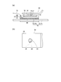
- FIG. 1 is a diagram illustrating a semiconductor device 1 according to a first embodiment.
- FIG. 1A is a plan view of the semiconductor device 1
- FIG. 1B is a cross-sectional view of the semiconductor device 1.
- 1 is an enlarged view of a main part of a semiconductor device 1 according to a first embodiment.
- 2A is an enlarged cross-sectional view of a main part of the semiconductor device 1, and
- FIG. 2B is an enlarged plan view of the main part of the semiconductor device 1.
- 3 is a flowchart of a method for manufacturing the semiconductor device according to the first embodiment.
- FIG. 6 is a process diagram of the method for manufacturing the semiconductor device according to the first embodiment.
- 4A is a diagram showing a substrate preparation process
- FIG. 4B is a diagram showing a semiconductor chip arrangement process
- FIG. 4C is a diagram showing a solder material arrangement process.
- FIG. 6 is a process diagram of the method for manufacturing the semiconductor device according to the first embodiment.
- FIG. 5A is a diagram showing a lead frame arranging step
- FIG. 5B is a diagram showing a joining step (reflow step)
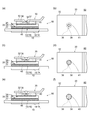
- FIG. 5C is a diagram showing a wire bonding step. It is a figure shown in order to demonstrate the effect of the manufacturing method of the semiconductor device concerning Embodiment 1.
- 6A is a cross-sectional view of the assembly 50 before the lead (lead frame) is arranged on the solder material
- FIG. 6B is a plan view of the assembly 50 before the lead is arranged on the solder material.
- FIG. 6 (c) is a cross-sectional view of the assembly 50 after the leads are arranged on the solder material
- FIG. 6 (d) is a plan view of the assembly 50 after the leads are arranged on the solder material.
- 6E is a cross-sectional view of the assembly 50 after the joining process
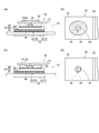
- FIG. 6F is a plan view of the assembly 50 after the joining process. It is a figure shown in order to demonstrate the effect of the manufacturing method of the semiconductor device concerning Embodiment 2.
- 7A is a cross-sectional view of the assembly 51 before the joining process (reflow process) is performed
- FIG. 7B is a plan view of the assembly 51 before the joining process (reflow process) is performed.
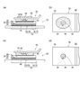
- FIG. 7 (d) is a top view of the assembly 51 in implementation of a joining process (reflow process). It is a figure shown in order to demonstrate the effect of the manufacturing method of the semiconductor device concerning Embodiment 3.
- 8A is a cross-sectional view of the assembly 52 before the joining process (reflow process) is performed
- FIG. 8B is a plan view of the assembly 52 before the joining process (reflow process) is performed.
- FIG. 8C is a cross-sectional view of the assembly 52 during the joining process (reflow process)
- FIG. 8D is a plan view of the assembly 52 during the joining process (reflow process).
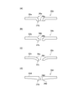
- FIG. 10 is an enlarged cross-sectional view of a main part showing convex portions and through holes of leads in semiconductor devices according to Modifications 1 to 4.
- 9 (a) to 9 (d) are enlarged cross-sectional views of the main parts showing the lead protrusions and through holes in the semiconductor devices according to the first to fourth modifications.
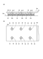
- 10 is an enlarged view of a main part in a semiconductor device according to Modification Example 5.
- FIG. 10A is an enlarged cross-sectional view of a main part of a semiconductor device according to Modification Example 5
- FIG. 10B is an enlarged plan view of a main part of the semiconductor device according to Modification Example 5.
- FIG. 10 is a view showing a semiconductor device 2 according to Modification 6;
- FIG. 10 is a view showing a semiconductor device 2 according to Modification 6;
- FIG. 11A is a perspective view of the semiconductor device 2
- FIG. 11B is a cross-sectional view of the semiconductor device 2.
- reference numeral 946 indicates solder
- reference numerals 960 and 962 indicate terminals
- reference numeral 970 indicates a wire
- reference numeral 980 indicates a resin.
- FIG. 13A is a view showing the state of the assembly before lead placement
- FIG. 13B is a view showing the state of the assembly after lead placement.
- Reference numerals 941 and 945 denote paste-like solder materials.
- the semiconductor device 1 according to Embodiment 1 includes a substrate 10, a semiconductor chip 20, leads 30, 62, 64, and solders 40, 46. And a wire 70, and are resin-sealed with a resin 80 except for the external connection terminals of the leads 30, 62 and 64 and a part of the heat-dissipating metal plate 18.
- the substrate 10 is a substrate having a semiconductor chip arrangement surface 12.
- an appropriate substrate for example, a printed circuit board
- the insulating substrate 14 and the insulating substrate 14 are formed on one surface, and the semiconductor chip arrangement surface 12 is formed.
- a DCB (Direct Copper Bonding) substrate having a circuit 16 and a heat radiating metal plate 18 formed on the other surface of the insulating substrate 14 is used. Note that the metal plate 18 for heat dissipation is exposed from the resin 80.
- the semiconductor chip 20 is arranged on the semiconductor chip arrangement surface 12, and the collector electrode 22 formed on one surface (the surface facing the semiconductor chip arrangement surface 12 or the surface on the substrate 10 side), and the other
- the emitter electrode 24 (electrode) and the emitter electrode 24 formed on the surface (the surface opposite to the surface facing the semiconductor chip arrangement surface 12 or the surface opposite to the surface on the substrate 10 side) are separated from each other.
- This is an IGBT (Insulated Gate Bipolar Transistor) having a gate electrode 26 formed at the position.
- the collector electrode 22 is bonded to the semiconductor chip placement surface 12 of the substrate 10 via the solder 46, and is connected to the outside via the solder 46, the substrate 10 (circuit 16), and the leads 64.
- the emitter electrode 24 is joined to the electrode connection piece 32 of the lead 30 via the solder 40, and is connected to the outside via the solder 40 and the lead 30 (external connection terminal 34).
- the leads 30, 62 and 64 are flat metal members and are formed by separating the lead frame.
- the leads 30, 62, and 64 have a larger cross-sectional area than the wire, and can pass a large current.
- the lead 30 has an electrode connection piece 32 for connecting to the emitter electrode 24 at one end, and an external connection terminal 34 for connecting to the outside at the other end.
- the electrode connecting piece 32 is formed on the semiconductor chip 20 side in a region where the electrode connecting piece 32 is joined to the solder 40, and on the top 37 of the convex portion 36, and from the surface on the semiconductor chip 20 side to the semiconductor chip 20 side. And a through hole 38 penetrating to the opposite surface.
- the lead 30 has a shape that is bent toward the semiconductor chip 20 at the convex portion 36 when viewed in cross section.
- the convex portion 36 has a shape that is stamped out toward the semiconductor chip 20 side.
- the side surface shape of the convex portion 36 is a narrow taper shape on the semiconductor chip 20 side, and the side surface shape of the convex portion (the cross-sectional shape of the side surface) is rounded.
- the side surface shape of the convex portion 36 is a Mt. Fuji shape having a top on the semiconductor chip 20 side and a wide skirt, or a trumpet shape on the opposite side to the semiconductor chip 20.
- the through hole 38 is formed in the top portion 37 of the convex portion 36 and penetrates from the surface on the semiconductor chip 20 side to the surface on the opposite side to the semiconductor chip 20 side.
- the through hole 38 has such a size that the solder material can come and go through the through hole 38 when the lead 30 is placed on the solder material before the joining step (that is, the solder material passes through the through hole 38). Therefore, it is a size that prevents the solder material from jumping out to an unintended area.
- the lead 62 has one end connected to the gate electrode 26 via a wire 70, and the other end serving as a terminal for external connection.
- the lead 64 is connected to the circuit 16 having one end connected to the collector electrode 22, and the other end serves as a terminal for external connection.
- the solders 40 and 46 are an alloy or metal having conductivity and adhesiveness.
- the solders 40 and 46 are melted and solidified by heating the solder material.
- the solder 40 joins the emitter electrode 24 and the electrode connection piece 32.
- the thickness of the solder 40 (solder thickness) is larger than the thickness of the solder 46 (solder between the substrate 10 and the semiconductor chip 20), for example, 300 ⁇ m or more.
- the solder 46 joins the collector electrode 22 and the semiconductor chip arrangement surface 12.
- the solder 46 is formed from a paste-like solder material (so-called cream solder) containing a solvent (specifically, flux), and is placed on the semiconductor chip placement surface 12 of the substrate 10 by printing and reflowed.
- the substrate 10 and the semiconductor chip 20 are bonded together by heating.
- the solder 46 does not have a situation in which stress (for example, thermal stress) acting on the solder is relaxed, and the conduction loss increases as the thickness increases. Therefore, the solder 46 is preferably relatively thin.
- the resin 80 an appropriate resin can be used.
- a manufacturing method of a semiconductor device according to Embodiment 1 includes a substrate preparation step S100, a semiconductor chip placement step S200, an assembly formation step S300, and a bonding A process S400, a wire bonding process S500, a resin sealing process S600, and a lead processing process S700 are included.
- Substrate preparation step S100 the substrate 10 is prepared (see FIG. 4A). Specifically, the substrate 10 is positioned and arranged on a predetermined jig.
- the semiconductor chip 20 is placed on the semiconductor chip placement surface 12 of the substrate 10 via the solder material 45 (see FIG. 4B). Specifically, first, a paste-like solder material 45 (for example, so-called cream solder) is printed on the semiconductor chip placement surface 12 of the substrate 10. Next, the semiconductor chip 20 is arranged on the semiconductor chip arrangement surface 12 so that the semiconductor chip arrangement surface 12 and the collector electrode 22 of the semiconductor chip 20 face each other with the solder material 45 interposed therebetween.
- a paste-like solder material 45 for example, so-called cream solder
- the solder material 45 is supplied by printing the solder material 45, but the solder material is supplied by a dispenser, the solder material is supplied by thread solder fed out by a solder feeder or the like, and melted.
- the solder material may be supplied by an appropriate method such as supplying the solder material by pouring it.
- cream solder is obtained by adding a flux to solder powder to form a paste with an appropriate viscosity.
- the flux is a component that volatilizes at a high temperature (for example, the melting temperature of solder).
- resin-based fluxes using rosin, modified rosin, synthetic resin, etc. as the main component are used.
- thixotropic agents, activators and solvents for activators, dispersion stabilizers, etc. are added. There is also.
- the assembly forming step S300 includes a solder material arranging step S310 and a lead frame arranging step S320.
- solder material placement step S310 In the solder material arranging step S310, the solder material 41 is arranged on the emitter electrode 24 of the semiconductor chip 20 (see FIG. 4C).
- a paste-like solder material containing a solvent is used as the solder material 41.
- a paste-like solder material specifically, so-called cream solder
- a solvent for example, flux
- a component that volatilizes at a high temperature for example, a melting temperature of solder
- solder material 41 can move through the through hole 38 in the subsequent lead frame placement step. Any other appropriate solder material may be used as long as it has a certain degree of viscosity.
- Lead frame placement step S320 In the lead frame arranging step, a protrusion 36 protruding to one surface side and a penetrating hole formed from one surface to the other surface opposite to the one surface are formed on the top portion 37 of the protrusion 36.
- the leads 62 and 64 in the lead frame 200 are also arranged at predetermined positions.
- solder material 41 it arranges
- the excessive solder material 41 moves through the through hole toward the side opposite to the semiconductor chip 20 side of the lead 30 (see FIGS. 6C and 6D). Therefore, the solder material 41 does not flow out to a region where the solder material 41 is not intended (for example, a region where the emitter electrode is not formed in a plan view). Even if the solder material flows out on the surface of the lead 30 opposite to the semiconductor chip 20 side, there is no electrode having a different potential around the surface, and it is difficult for trouble to occur.
- the lead 30 having the electrode connection piece 32 is in a state where the emitter electrode 24 and the electrode connection piece 32 face each other with the solder material 41 interposed therebetween, and the protrusion 36 protrudes toward the emitter electrode 24 side.
- the assembly 50 can be formed (see FIG. 5A).
- Joining process S400
- the assembly 50 is put into a reflow furnace (not shown) and heated to melt the solder materials 41 and 45, and then the solder materials 41 and 45 are solidified to form the solder 40. , 46 (see FIG. 5B).
- excess solder material moves to the surface of the lead 30 opposite to the semiconductor chip 20 side through the through hole 38 (see FIGS. 6E and 6F).
- a gas such as flux is released to the outside through the through hole 38.
- the semiconductor chip placement surface 12 of the substrate 10 and the emitter electrode 24 of the semiconductor chip 20 are joined via the solder 46, and the collector electrode 22 of the semiconductor chip 20 and the electrode connection piece 32 of the lead 30 are joined with the solder 40. Join through.
- the electrode connection piece 32 includes the protrusion 36 protruding toward the semiconductor chip 20 in the region where the electrode connection piece 32 is bonded to the solder 40, and Since it has a through hole 38 formed on the top 37 of the convex portion 36 and penetrated from the surface on the semiconductor chip 20 side to the surface on the opposite side to the semiconductor chip 20 side, the lead is placed on the solder material 41 in the manufacturing process. When 30 is disposed, excess solder material can flow through the through hole 38 to the surface of the lead 30 opposite to the semiconductor chip 20.
- the thickness of the solder 40 is kept to a certain level or more, even when 30 leads are arranged on the solder material 41 (before the joining process), the excessive solder material 41 is protruded to an undesired place. This can prevent the reliability of the semiconductor device from being lowered.
- the electrode connection piece 32 has the convex portion 36 protruding toward the semiconductor chip 20 in the region where the electrode connection piece 32 is bonded to the solder 40, and therefore, compared with the conventional semiconductor device.
- the contact area between the lead 30 and the solder 40 is increased.
- the electrode connection piece 32 is formed on the top portion 37 of the convex portion 36 and penetrates from the surface on the semiconductor chip 20 side to the surface opposite to the semiconductor chip 20 side. Therefore, when the lead 30 is disposed on the solder material 41, excess solder material 41 can flow through the through hole 38 to the surface of the lead 30 opposite to the semiconductor chip 20. it can.
- the solder 40 exists in the through hole 38 and on the surface of the lead 30 opposite to the semiconductor chip 20 side, the contact area between the lead 30 and the solder 40 becomes larger. Therefore, the bonding strength between the lead 30 and the solder 40 is increased, and the reliability of the semiconductor device is increased.
- the lead 30 has a shape that is bent toward the semiconductor chip 20 at the portion of the convex portion 36 when viewed in cross section.
- the surplus solder material 41 that has passed through the through hole 38 can be wound around the back side of the surface of the lead 30 on the semiconductor chip side. Therefore, the portion of the lead 30 near the opening of the through hole 38 comes into contact with the solder 40 on both sides of the semiconductor chip 20 and the side opposite to the semiconductor chip 20. Therefore, the bonding strength between the lead 30 and the solder 40 is further increased, and the reliability of the semiconductor device is hardly lowered.
- the side surface shape of the convex portion 36 is a narrow tapered shape on the semiconductor chip 20 side. Compared with the case of being vertical, the contact area between the lead 30 and the solder 40 is increased. Therefore, the bonding strength between the lead 30 and the solder 40 is further increased, and the reliability of the semiconductor device is increased.
- the convex portion 36 has a shape in which the lead 30 is bent toward the semiconductor chip 20 when viewed in a cross section, and the side surface of the convex portion 36 has a narrow tapered shape on the semiconductor chip 20 side.
- the lead 30 is viewed from the side opposite to the semiconductor chip 20 side, a concave portion having a tapered side surface is formed.
- the solder material 41 that has flowed to the opposite side tends to stagnate in the vicinity of the through-hole 38, and when such a solder material 41 is solidified, it becomes solder having a shape like a screw head (a shape like a conical shape with the apex on the semiconductor chip side). . Therefore, the lead 30 and the solder 40 are less likely to be peeled off, and the bonding strength between the lead 30 and the solder 40 can be further increased.
- the side surface of the convex portion 36 has a rounded shape, and thus the lead 30 (lead frame) on the solder material 41.
- the lead 30 lead frame
- the thickness of the solder 40 is 300 ⁇ m or more, and therefore, between the semiconductor chip 20 and the lead 30.
- the stress (for example, thermal stress) acting on the solder 40 can be relaxed, and problems such as cracks in the solder 40 are less likely to occur.
- the thickness of the solder 40 is preferably 400 ⁇ m or more and the thickness of the solder 40 is more preferably 500 ⁇ m or more in order to make the above-described problems less likely to occur.
- the protrusion 36 is formed on one surface side, and is formed on the top portion 37 of the protrusion 36.
- a lead 30 having an electrode connection piece 32 having a through-hole 38 penetrating to the other surface opposite to the emitter electrode 24 and the electrode connection piece 32 with the solder material 41 interposed therebetween, and
- the assembly 50 is formed by arranging the protruding portions 36 so as to protrude toward the emitter electrode 24 side, and in the joining step, the solder material 41 is melted and then solidified, whereby the emitter electrode 24 and the electrode are formed.
- the excess solder material 41 passes through the through hole 38 and is opposite to the semiconductor chip 20 in the lead 30. Can to flow towards the surface of the side. Therefore, in the case where the thickness of the solder 40 is kept to a certain level or more, even when the lead 30 is arranged on the solder material 41 before the joining process, the excess solder material 41 is prevented from protruding to an undesired place. Thus, a semiconductor device in which reliability is hardly lowered can be manufactured.
- the solder material 41 is made of a paste-like solder material containing a solvent, and since such a solder material has fluidity, the lead 30 is placed on the solder material 41. When the is disposed, surplus solder material 41 can flow through the through hole 38 toward the surface of the lead 30 opposite to the semiconductor chip 20.
- the manufacturing method of the semiconductor device according to the second embodiment basically includes the same steps as the manufacturing method of the semiconductor device according to the first embodiment, but the position where the solder material is disposed is the manufacturing method of the semiconductor device according to the first embodiment. It is different from the method.
- the solder material 41 is not disposed between the emitter electrode 24 and the electrode connection piece 32 in the assembly formation process (lead frame arrangement process).
- a solder material 42 is disposed in a predetermined region including the through hole 38 on the surface opposite to the surface on the emitter electrode 24 side (surface opposite to the surface on which the convex portion is formed) (FIG. 7A). )reference.).
- the lead 30 in which the solder material 42 is disposed in a predetermined region including the through hole 38 on the surface of the electrode connection piece 32 opposite to the surface on the emitter electrode 24 side is connected to the emitter electrode 24 and the electrode connection piece 32.
- the convex portion 36 protrudes toward the emitter electrode 24 to form the assembly 51.
- a predetermined portion (a plurality of portions are preferable) of the lead 30 (lead frame) is sandwiched and fixed by a predetermined jig from above and below to form an emitter electrode. 24 and the electrode connection piece 32 are separated from each other at a predetermined interval.
- the solder material 42 disposed in a predetermined region including the through hole 38 on the surface opposite to the surface on the emitter electrode 24 side of the electrode connecting piece 32 is melted and the emitter electrode 24 is connected to the emitter electrode 24 through the through hole 38.
- the electrode connection pieces 32 see FIG. 7B.
- the solder material 42 is solidified when the solder material 41 is filled between the emitter electrode 24 and the electrode connection piece 32. Thereby, the emitter electrode 24 and the electrode connection piece 32 can be joined via the solder 40.
- the semiconductor device manufacturing method according to the second embodiment is different from the semiconductor device manufacturing method according to the first embodiment in the position at which the solder material is disposed.
- the electrode connecting piece 32 having a projecting portion 36 that protrudes from the top surface 37 and a through hole 38 that is formed on the top portion 37 of the projecting portion 36 and penetrates from one surface to the other surface opposite to the one surface.
- the lead 30 in which the solder material 42 is arranged in a predetermined region including the through hole 38 on the other surface is in a state where the emitter electrode 24 and the electrode connection piece 32 face each other at a predetermined interval, and the convex portion 36. Are arranged so as to protrude toward the emitter electrode 24 side, and an assembly 51 is formed.
- the solder material 42 is melted and the emitter electrode 24 and the electrode connecting piece 32 are connected through the through hole 38.
- solder materials 2 after the solder material 42 is solidified, the emitter electrode 24 and the electrode connecting piece 32 are joined via the solder 40, so that a certain thickness or more (before the joining process) Therefore, it is possible to prevent the excessive solder material from protruding to an undesired place. As a result, it is possible to manufacture a semiconductor device whose reliability is not easily lowered.
- solder material 42 is made of a paste-like solder material, the solder material is easily melted in the joining step, and when the solder material 41 is melted, It becomes easy to allow the solder material 41 to flow between the emitter electrode 24 and the electrode connecting piece 32 through the through hole 38.
- the lead 30 having the tapered shape in which the side surface shape of the convex portion 36 is narrow on the semiconductor chip 20 side is disposed.
- the solder material 41 supplied between the emitter electrode 24 and the electrode connection piece 32 is unlikely to flow backward from the through hole 38, and the solder material 41 can be supplied efficiently between the emitter electrode 24 and the electrode connection piece 32.
- the side surface of the convex portion 36 is rounded, so that the solder material 42 is easy to move, and the emitter electrode 24 and the electrode connection piece.
- the solder material 41 can be efficiently supplied between the two.
- the semiconductor device manufacturing method according to the second embodiment has the same configuration as that of the semiconductor device manufacturing method according to the first embodiment except for the position where the solder material is disposed, and thus the semiconductor device according to the first embodiment. This method has the corresponding effect among the effects of the manufacturing method.
- the manufacturing method of the semiconductor device according to the third embodiment basically includes the same steps as the manufacturing method of the semiconductor device according to the second embodiment, but a solder material is also provided between the emitter electrode 24 and the electrode connection piece 32.
- the arrangement is different from the semiconductor device manufacturing method according to the second embodiment. That is, in the method for manufacturing a semiconductor device according to the third embodiment, in the assembly forming process, only a predetermined region including the through hole 38 on the surface opposite to the surface on the emitter electrode 24 side of the electrode connection piece 32 is used.
- a solder material 43 is also disposed in a part between the emitter electrode 24 and the electrode connection piece 32 (see FIGS. 8A and 8B).
- solder material supplied between the emitter electrode 24 and the electrode connection piece 32 through the through hole 38 and the solder material previously disposed between the emitter electrode 24 and the electrode connection piece 32 are formed. They are mixed and filled between the emitter electrode 24 and the electrode connecting piece 32 with a solder material and solidified (see FIGS. 8C and 8D).
- the method for manufacturing a semiconductor device according to the third embodiment is that the solder material is also disposed between the emitter electrode 24 and the electrode connection piece 32 in the case of the method for manufacturing a semiconductor device according to the second embodiment.
- the protrusion 36 is formed on one surface side, and the top portion 37 of the protrusion 36 is formed.
- An electrode connection piece 32 having a through hole 38 penetrating from one surface to the other surface opposite to the one surface, and a solder material 42 in a predetermined region including the through hole 38 on the other surface.
- the solder material 42 is melted and poured into the emitter electrode 24 and the electrode connection piece 32 through the through hole 38, and then the solder material 42 is solidified, whereby the emitter electrode 24 and the electrode connection piece are solidified. Since the lead 30 is not disposed on the solder material (before the joining step) having a certain thickness or more (before the joining process), the excess solder material protrudes to an undesired place. Can be prevented. As a result, it is possible to manufacture a semiconductor device whose reliability is not easily lowered.
- the solder material 43 is also disposed in a part between the emitter electrode 24 and the electrode connection piece 32.
- the space between the emitter electrode 24 and the electrode connection piece 32 can be filled with the solder material in a short time, and the semiconductor device can be manufactured efficiently.
- the semiconductor device manufacturing method according to the third embodiment is different from the semiconductor device manufacturing method according to the second embodiment in that the solder material is also disposed between the emitter electrode 24 and the electrode connection piece 32. Therefore, the semiconductor device manufacturing method according to the second embodiment has a corresponding effect.
- the convex portion 36 has a tapered shape with a curved side surface, but the present invention is not limited to this.
- the convex portion may have a taper shape with straight sides (see FIG. 9A), and the convex portion has a flat portion at the top, and a through hole is formed in a part thereof. It is good also as doing (refer FIG.9 (b)).
- the convex portion may have a shape in which the lead 30 is bent more gently toward the semiconductor chip (see FIG. 9C).
- the convex portion has a shape in which the lead 30 is bent toward the semiconductor chip 20 when viewed in cross section, but the present invention is not limited to this. is not.
- the thickness of the lead in the vicinity of the through hole may be increased to form the convex portion (see FIG. 9D).
- a semiconductor chip in which the emitter electrode is divided into a plurality of electrodes may be used as the semiconductor chip.
- the semiconductor device is a semiconductor device including one semiconductor chip.
- the semiconductor device may be a semiconductor device including two semiconductor chips (see FIG. 11) or a semiconductor device including three or more semiconductor chips.
- the following semiconductor device in which two semiconductor chips are cascode-connected can be considered.
- the emitter electrode 24f of the semiconductor chip 20f is electrically connected to the lead 30f
- the collector electrode 22f of the semiconductor chip 20f is connected to the lead 30g via the circuit 16f of the substrate 10f.
- it is electrically connected to the emitter electrode 24g of the semiconductor chip 20g via a lead 30g.
- the collector electrode 22g of the semiconductor chip 20g is connected to a lead 66 via a circuit 16g.
- the leads 30f and 30g may be formed with convex portions and through holes.
- one lead is used for the convex portion and the through hole, but the present invention is not limited to this.
- a lead having two or more protrusions and through holes may be used.
- the semiconductor chip 20 is a three-terminal IGBT, but the present invention is not limited to this.
- the semiconductor chip 20 may be another three-terminal semiconductor element (for example, MOSFET), the semiconductor chip 20 may be a two-terminal semiconductor element (for example, a diode), or the semiconductor chip 20 may be a semiconductor element having four or more terminals (4 The terminal may be a thyristor, for example.
- the semiconductor device is a so-called vertical semiconductor device having a collector electrode on one surface of a semiconductor chip and an emitter electrode and a gate electrode on the other surface. Is not limited to this.
- the semiconductor device may be a so-called horizontal semiconductor device having all electrodes on the surface opposite to the substrate side.
- SYMBOLS 1 Semiconductor device 10, 10a, 10b ... Board
- electrode connection piece 34 ... external connection terminal, 36, 36a, 36b, 36c, 36d, 36f, 36g ... convex part, 37, 37a, 37b, 37c, 37d, 36f, 36g ... top of convex part, 38, 38a, 38b, 38c, 38d, 38f, 8 g ... through hole, 40, 46 ... solder, 41,42,43,45 ... solder material, 50, 51, 52 ... assembly, 70 ... wire, 80 ... resin
Landscapes
- Lead Frames For Integrated Circuits (AREA)
- Die Bonding (AREA)
Abstract
本発明の半導体装置1は、半導体チップ配置面12を有する基板10と、半導体チップ配置面12上に配置され、基板10側の面とは反対側の面に形成された電極24を有する半導体チップ20と、電極24とはんだ40を介して接合された電極接続片32を有するリード30とを備え、電極接続片32は、はんだ40と接合する領域において、半導体チップ20側に突出した凸部36と、凸部36の頂上部37に形成され、半導体チップ20側の面から半導体チップ20側とは反対側の面まで貫通された貫通孔38とを有することを特徴とする。 本発明の半導体装置によれば、信頼性が低下し難い半導体装置を提供することができる。
Description
本発明は、半導体装置及び半導体装置の製造方法に関する。
従来、半導体チップとリードとがはんだを介して接合された半導体装置を製造する半導体装置の製造方法が知られている(例えば、特許文献1参照。)。
特許文献1に記載の従来の半導体装置900は、図12に示すように、半導体チップ配置面912を有する基板910と、半導体チップ配置面912上に配置され、基板910側の面(半導体チップ配置面12と対向する面)に形成されたコレクタ電極922、並びに、基板910側の面とは反対側の面(半導体チップ配置面12と対向する面とは反対側の面)に形成されたエミッタ電極924(電極)及びエミッタ電極924とは離間した位置に形成されたゲート電極926を有する半導体チップ920と、電極接続片932を有し、電極接続片932がエミッタ電極924とはんだ940を介して接合されたリード930とを備える
従来の半導体装置900によれば、電極接続片932がエミッタ電極924とはんだ940を介して接合されている、すなわち、半導体チップ920とリード930とがはんだ940のみを介して(ワイヤ等の介在部材を介さずに)直接接続されているため、半導体装置900は、電流容量が大きく、大電流を使用する電子機器(例えば、電源)に適した半導体装置となる。
ところで、一般に、半導体チップとリードとの間のはんだに作用する応力(例えば熱応力)を緩和するためには、はんだの厚みをある一定以上の厚さに保つことが有効であることが知られている(例えば、特許文献2参照。)。
しかしながら、従来の半導体装置の製造過程において、ペースト状のはんだ材941をある一定以上の厚さとすると、はんだ材941の上にリード930を配置したときにはんだ材941が潰れて余剰なはんだ材が所望しない場所にはみ出してしまうおそれがあり、半導体装置の信頼性が低下するおそれがある、という問題がある(図13参照。)。
そこで、本発明は、上記した問題を解決するためになされたものであり、信頼性が低下し難い半導体装置を提供することを目的とする。また、そのような半導体装置を製造するための半導体装置の製造方法を提供することを目的とする。
[1]本発明の半導体装置は、半導体チップ配置面を有する基板と、前記半導体チップ配置面上に配置され、前記半導体チップ配置面と対向する面とは反対側の面に形成された電極を有する半導体チップと、前記電極とはんだを介して接合された電極接続片を有するリードとを備え、前記電極接続片は、前記はんだと接合する領域において、前記半導体チップ側に突出した凸部と、前記凸部の頂上部に形成され、前記半導体チップ側の面から前記半導体チップ側とは反対側の面まで貫通された貫通孔とを有することを特徴とする。
[2]本発明の半導体装置において、前記リードは、断面で見たときに、前記凸部の部分で半導体チップ側に折り曲げられた形状を有することが好ましい。
[3]本発明の半導体装置においては、前記凸部の側面形状は、前記半導体チップ側が狭いテーパ形状であることが好ましい。
[4]本発明の半導体装置においては、前記凸部の側面形状は、丸みを帯びた形状になっていることが好ましい。
[5]本発明の半導体装置においては、前記はんだの厚さは、300μm以上であることが好ましい。
[6]本発明の第1の半導体装置の製造方法は、上記[1]~[5]のいずれかに記載の半導体装置を製造するための半導体装置の製造方法であって、基板上に半導体チップを配置する半導体チップ配置工程と、一方の面側に突出した凸部と、前記凸部の頂上部に形成され、前記一方の面から前記一方の面とは反対側の他方の面まで貫通された貫通孔とを有する電極接続片を有するリードを、前記半導体チップの電極と前記電極接続片とがはんだ材を挟んで対向した状態、かつ、前記凸部が前記電極側に向かって突出した状態となるように配置して組立体を形成する組立体形成工程と、前記はんだ材を溶融した後で固化することにより、前記電極と前記電極接続片とをはんだを介して接合する接合工程とを含むことを特徴とする。
[7]本発明の第2の半導体装置の製造方法は、上記[1]~[5]のいずれかに記載の半導体装置を製造するための半導体装置の製造方法であって、基板上に半導体チップを配置する半導体チップ配置工程と、一方の面側に突出した凸部と、前記凸部の頂上部に形成され、前記一方の面から前記一方の面とは反対側の他方の面まで貫通された貫通孔とを有する電極接続片を有し、前記他方の面における、前記貫通孔を含む所定の領域にはんだ材が配置されたリードを、前記半導体チップの電極と前記電極接続片とが所定の間隔で対向した状態、かつ、前記凸部が前記電極側に向かって突出した状態となるように配置して組立体を形成する組立体形成工程と、前記はんだ材を溶融して前記貫通孔を通して前記電極と前記電極接続片との間に前記はんだ材を流し込んだ後で前記はんだ材を固化することにより、前記電極と前記電極接続片とをはんだを介して接合する接合工程とを含むことを特徴とする。
[8]本発明の半導体装置の製造方法において、前記組立体形成工程においては、前記電極と前記電極接続片の間のうちの一部にもはんだ材が配置されていることが好ましい。
[9]本発明の半導体装置の製造方法において、前記組立体形成工程においては、断面で見たときに、前記凸部の部分で半導体チップ側に折り曲げられた形状を有する前記リードを配置することが好ましい。
[10]本発明の半導体装置の製造方法において、前記組立体形成工程においては、前記凸部の側面形状が、前記半導体チップ側が狭いテーパ形状である前記リードを配置することが好ましい。
[11]本発明の半導体装置の製造方法において、前記組立体形成工程においては、前記凸部の側面形状が、丸みを帯びた形状になっている前記リードを配置することが好ましい。
[12]本発明の半導体装置の製造方法において、前記はんだ材は、溶剤を含有するペースト状のはんだ材からなることが好ましい。
本発明の半導体装置によれば、電極接続片は、はんだと接合する領域において、半導体チップ側に突出した凸部と、凸部の頂上部に形成され、半導体チップ側の面から半導体チップ側とは反対側の面まで貫通された貫通孔とを有するため、製造過程において、はんだ材上にリードを配置したときに、余剰なはんだ材を貫通孔を通してリードにおける半導体チップとは反対側の面に流れさせることができる。従って、はんだの厚みをある一定以上の厚さに保つ場合において、(接合工程前の)はんだ材上にリードを配置したときでも、余剰なはんだ材が所望しない場所にはみ出すことを防ぐことができ、半導体装置の信頼性が低下し難くなる。
また、本発明の半導体装置によれば、電極接続片は、はんだと接合する領域において、半導体チップ側に突出した凸部を有するため、従来の半導体装置と比較して、リードとはんだとの接触面積が大きくなる。
また、本発明の半導体装置によれば、電極接続片は、凸部の頂上部に形成され、半導体チップ側の面から半導体チップ側とは反対側の面まで貫通された貫通孔とを有するため、はんだ材上にリードを配置したときに、余剰なはんだ材を貫通孔を通してリードにおける半導体チップとは反対側の面に流れさせることができる。従って、貫通孔内及びリードにおける半導体チップ側とは反対側の面にもはんだが存在することになるため、リードとはんだとの接触面積がより大きくなる。
従って、リードとはんだとの接合強度が高くなり、半導体装置の信頼性が高くなる。
また、本発明の半導体装置によれば、電極接続片は、凸部の頂上部に形成され、半導体チップ側の面から半導体チップ側とは反対側の面まで貫通された貫通孔とを有するため、はんだ材上にリードを配置したときに、余剰なはんだ材を貫通孔を通してリードにおける半導体チップとは反対側の面に流れさせることができる。従って、貫通孔内及びリードにおける半導体チップ側とは反対側の面にもはんだが存在することになるため、リードとはんだとの接触面積がより大きくなる。
従って、リードとはんだとの接合強度が高くなり、半導体装置の信頼性が高くなる。
本発明の第1の半導体装置の製造方法によれば、組立体形成工程において、一方の面側に突出した凸部と、凸部の頂上部に形成され、一方の面から一方の面とは反対側の他方の面まで貫通された貫通孔とを有する電極接続片を有するリードを、電極と電極接続片とがはんだ材を挟んで対向した状態、かつ、凸部が電極側に向かって突出した状態となるように配置して組立体を形成し、接合工程において、はんだ材を溶融した後で固化することにより、電極と電極接続片とをはんだを介して接合するため、はんだ材上にリードを配置したときに、余剰なはんだ材を貫通孔を通してリードにおける半導体チップとは反対側の面に向かって流れさせることができる。従って、はんだの厚みをある一定以上の厚さに保つ場合において、はんだ材上にリードを配置したときでも、余剰なはんだ材が所望しない場所にはみ出すことを防ぐことができ、信頼性が低下し難い半導体装置を製造することができる。
本発明の第2の半導体装置の製造方法によれば、組立体形成工程において、一方の面側に突出した凸部と、凸部の頂上部に形成され、一方の面から一方の面とは反対側の他方の面まで貫通された貫通孔とを有する電極接続片を有し、他方の面における、貫通孔を含む所定の領域にはんだ材が配置されたリードを、電極と電極接続片とが所定の間隔で対向した状態、かつ、凸部が電極側に向かって突出した状態となるように配置して組立体を形成し、接合工程において、はんだ材を溶融して貫通孔を通して電極と電極接続片との間にはんだ材を流し込んだ後ではんだ材を固化することにより、電極と電極接続片とをはんだを介して接合するため、接合工程前のはんだ材を厚くしすぎることがなく、ある一定以上の厚さのはんだ材上にリードを配置する、ということもない。従って、余剰なはんだ材が所望しない場所にはみ出すことを防ぐことができる。その結果、信頼性が低下し難い半導体装置を製造することができる。
以下、本発明の半導体装置の製造方法について、図に示す実施形態に基づいて説明する。なお、各図面は模式図であり、必ずしも実際の寸法を厳密に反映したものではない。
[実施形態1]
1.実施形態1における半導体装置1の構成
実施形態1に係る半導体装置1は、図1及び図2に示すように、基板10と、半導体チップ20と、リード30,62,64と、はんだ40,46と、ワイヤ70とを備え、リード30,62,64の外部接続端子及び放熱性の金属板18の一部を除いて樹脂80で樹脂封止されている。
1.実施形態1における半導体装置1の構成
実施形態1に係る半導体装置1は、図1及び図2に示すように、基板10と、半導体チップ20と、リード30,62,64と、はんだ40,46と、ワイヤ70とを備え、リード30,62,64の外部接続端子及び放熱性の金属板18の一部を除いて樹脂80で樹脂封止されている。
基板10は、半導体チップ配置面12を有する基板である。基板10としては適宜の基板(例えば、プリント基板)を用いることができるが、実施形態1においては、絶縁性基板14と、絶縁性基板14の一方の面に形成され、半導体チップ配置面12を有する回路16と、絶縁性基板14の他方の面に形成された放熱用の金属板18とを有するDCB(Direct Cоpper Bonding)基板を用いる。なお、放熱用の金属板18は樹脂80から露出している。
半導体チップ20は、半導体チップ配置面12上に配置されており、一方の面(半導体チップ配置面12と対向する面。あるいは、基板10側の面)に形成されたコレクタ電極22、並びに、他方の面(半導体チップ配置面12と対向する面とは反対側の面。あるいは、基板10側の面とは反対側の面)に形成されたエミッタ電極24(電極)及びエミッタ電極24とは離間した位置に形成されたゲート電極26を有するIGBT(Insulated Gate Bipolar Transistor)である。
コレクタ電極22は、基板10の半導体チップ配置面12とはんだ46を介して接合されており、はんだ46、基板10(回路16)及びリード64を介して外部と接続される。
エミッタ電極24は、リード30の電極接続片32とはんだ40を介して接合されており、はんだ40及びリード30(外部接続端子34)を介して外部と接続される。
エミッタ電極24は、リード30の電極接続片32とはんだ40を介して接合されており、はんだ40及びリード30(外部接続端子34)を介して外部と接続される。
リード30,62,64は、平板状の金属部材であり、リードフレームを切り離して形成されたものである。リード30,62,64はワイヤよりも断面積が大きく、大電流を流すことができる。
リード30は、一方の端部にエミッタ電極24と接続するための電極接続片32を有し、他方の端部に外部と接続するための外部接続端子34を有する。
電極接続片32は、はんだ40と接合する領域において、半導体チップ20側に突出した凸部36と、凸部36の頂上部37に形成され、半導体チップ20側の面から半導体チップ20側とは反対側の面まで貫通された貫通孔38とを有する。
リード30は、断面で見たときに、凸部36の部分で半導体チップ20側に折り曲げられた形状を有する。凸部36は、半導体チップ20側に向かって打ち出し加工されたような形状を有する。凸部36の側面形状は、半導体チップ20側が狭いテーパ形状であり、凸部の側面形状(側面の断面形状)は、丸みを帯びた形状をしている。言い換えると、凸部36の側面形状は、半導体チップ20側が頂上部となり、かつ、裾野が広い富士山型の形状、あるいは、半導体チップ20とは反対側が広いラッパ型の形状をしている。
電極接続片32を半導体チップ20側とは反対側の面からみると、凸部36の形状に対応した形状の凹部があるように見える。言い換えると、半導体チップ20側とは反対側の面から半導体チップ20側に向かうに従って狭くなっている凹部があるように見える。凹部の最底部には貫通孔38がある。凹部内にはエミッタ電極24と電極接続片32との間のはんだ40から流れ出たはんだが入り込んでおり、当該はんだは、貫通孔38近傍のリード30における半導体チップ20側とは反対側からリード30に接している。
貫通孔38は、凸部36の頂上部37に形成され、半導体チップ20側の面から半導体チップ20側とは反対側の面まで貫通されている。貫通孔38は、接合工程前にリード30をはんだ材の上に配置したときに、はんだ材が貫通孔38を介して行き来できる程度の大きさである(すなわち、はんだ材が貫通孔38を介して十分行き来できず、意図しない領域にはんだ材が飛び出してしまうことを防ぐことができる程度の大きさである)。
リード62は、一方の端部がワイヤ70を介してゲート電極26と接続されており、他方の端部が外部接続用の端子となっている。リード64は、一方の端部がコレクタ電極22と接続された回路16と接続されており、他方の端部が外部接続用の端子となっている。
はんだ40,46は、導電性及び接着性を有する合金又は金属である。はんだ40、46ははんだ材を加熱することにより溶融して固化したものである。
はんだ40は、エミッタ電極24と電極接続片32とを接合している。はんだ40の厚さ(はんだ厚)は、はんだ46(基板10と半導体チップ20との間のはんだ)の厚さよりも厚く、例えば300μm以上である。
はんだ46は、コレクタ電極22と半導体チップ配置面12を接合している。はんだ46は、溶剤(具体的にはフラックス)を含有するペースト状のはんだ材(いわゆるクリームはんだ)から形成されたものであり、印刷により基板10の半導体チップ配置面12上に配置され、リフローして加熱することにより基板10と半導体チップ20とを接合する。なお、はんだ46は、はんだ40の場合と異なり、はんだに作用する応力(例えば熱応力)を緩和するという事情がなく、厚くなると導通損失が大きくなるため、比較的薄い方が好ましい。
はんだ40は、エミッタ電極24と電極接続片32とを接合している。はんだ40の厚さ(はんだ厚)は、はんだ46(基板10と半導体チップ20との間のはんだ)の厚さよりも厚く、例えば300μm以上である。
はんだ46は、コレクタ電極22と半導体チップ配置面12を接合している。はんだ46は、溶剤(具体的にはフラックス)を含有するペースト状のはんだ材(いわゆるクリームはんだ)から形成されたものであり、印刷により基板10の半導体チップ配置面12上に配置され、リフローして加熱することにより基板10と半導体チップ20とを接合する。なお、はんだ46は、はんだ40の場合と異なり、はんだに作用する応力(例えば熱応力)を緩和するという事情がなく、厚くなると導通損失が大きくなるため、比較的薄い方が好ましい。
樹脂80は、適宜の樹脂を用いることができる。
2.実施形態1に係る半導体装置の製造方法
実施形態1に係る半導体装置の製造方法は、図3に示すように、基板準備工程S100と、半導体チップ配置工程S200と、組立体形成工程S300と、接合工程S400と、ワイヤボンディング工程S500と、樹脂封止工程S600と、リード加工工程S700とを含む。
実施形態1に係る半導体装置の製造方法は、図3に示すように、基板準備工程S100と、半導体チップ配置工程S200と、組立体形成工程S300と、接合工程S400と、ワイヤボンディング工程S500と、樹脂封止工程S600と、リード加工工程S700とを含む。
(1)基板準備工程S100
基板準備工程S100においては、基板10を準備する(図4(a)参照。)。具体的には、所定の治具上に基板10を位置決めして配置する。
基板準備工程S100においては、基板10を準備する(図4(a)参照。)。具体的には、所定の治具上に基板10を位置決めして配置する。
(2)半導体チップ配置工程S200
半導体チップ配置工程S200においては、基板10の半導体チップ配置面12上にはんだ材45を介して半導体チップ20を配置する(図4(b)参照。)。具体的には、まず、基板10の半導体チップ配置面12上にペースト状のはんだ材45(例えば、いわゆるクリームはんだ)を印刷する。次に、半導体チップ配置面12と半導体チップ20のコレクタ電極22とがはんだ材45を挟んで対向した状態となるように半導体チップ配置面12上に半導体チップ20を配置する。
なお、実施形態1においては、はんだ材45を印刷することによりはんだ材を供給しているが、ディスペンサによってはんだ材を供給する、はんだフィーダ等で送り出した糸はんだによってはんだ材を供給する、溶融したはんだ材を流し込むことによってはんだ材を供給する等、適宜の方法ではんだ材を供給してもよい。
半導体チップ配置工程S200においては、基板10の半導体チップ配置面12上にはんだ材45を介して半導体チップ20を配置する(図4(b)参照。)。具体的には、まず、基板10の半導体チップ配置面12上にペースト状のはんだ材45(例えば、いわゆるクリームはんだ)を印刷する。次に、半導体チップ配置面12と半導体チップ20のコレクタ電極22とがはんだ材45を挟んで対向した状態となるように半導体チップ配置面12上に半導体チップ20を配置する。
なお、実施形態1においては、はんだ材45を印刷することによりはんだ材を供給しているが、ディスペンサによってはんだ材を供給する、はんだフィーダ等で送り出した糸はんだによってはんだ材を供給する、溶融したはんだ材を流し込むことによってはんだ材を供給する等、適宜の方法ではんだ材を供給してもよい。
なお、クリームはんだは、はんだ粉末にフラックスを添加して、適当な粘度のペースト状にしたものである。フラックスは、高温(例えば、はんだの溶融温度)で揮発する成分である。フラックスとしては、ロジン、変性ロジン、合成樹脂などを主成分として用いた樹脂系フラックスが用いられ、さらに、チクソトロピック剤や、活性剤および活性剤用の溶剤、分散安定剤などが添加される場合もある。
(3)組立体形成工程S300
組立体形成工程S300は、はんだ材配置工程S310とリードフレーム配置工程S320を含む。
組立体形成工程S300は、はんだ材配置工程S310とリードフレーム配置工程S320を含む。
(3-1)はんだ材配置工程S310
はんだ材配置工程S310においては、半導体チップ20のエミッタ電極24上にはんだ材41を配置する(図4(c)参照。)。はんだ材41としては、溶剤を含有するペースト状のはんだ材を用いる。実施形態1においては、溶剤として、高温(例えば、はんだの溶融温度)で揮発する成分を含有する溶剤(例えば、フラックス)を含有するペースト状のはんだ材(具体的には、いわゆるクリームはんだ)を用いる。なお、溶剤として、高温で揮発する成分を含有する溶剤以外の溶剤を含有するペースト状のはんだ材を用いてもよいし、後のリードフレーム配置工程において、貫通孔38を通してはんだ材41が移動できる程度の粘度があるはんだ材であれば、他の適宜のはんだ材を用いてもよい。
はんだ材配置工程S310においては、半導体チップ20のエミッタ電極24上にはんだ材41を配置する(図4(c)参照。)。はんだ材41としては、溶剤を含有するペースト状のはんだ材を用いる。実施形態1においては、溶剤として、高温(例えば、はんだの溶融温度)で揮発する成分を含有する溶剤(例えば、フラックス)を含有するペースト状のはんだ材(具体的には、いわゆるクリームはんだ)を用いる。なお、溶剤として、高温で揮発する成分を含有する溶剤以外の溶剤を含有するペースト状のはんだ材を用いてもよいし、後のリードフレーム配置工程において、貫通孔38を通してはんだ材41が移動できる程度の粘度があるはんだ材であれば、他の適宜のはんだ材を用いてもよい。
(3-2)リードフレーム配置工程S320
リードフレーム配置工程においては、一方の面側に突出した凸部36と、凸部36の頂上部37に形成され、一方の面から一方の面とは反対側の他方の面まで貫通された貫通孔38とを有する電極接続片32を有するリード30(リード30が連結されているリードフレーム)を、エミッタ電極24と電極接続片32とがはんだ材41を挟んで対向した状態、かつ、凸部36がエミッタ電極24側に向かって突出した状態となるように配置する(図5(a)参照。)。このとき、リードフレーム200内のリード62,64も所定の位置に配置される。
リードフレーム配置工程においては、一方の面側に突出した凸部36と、凸部36の頂上部37に形成され、一方の面から一方の面とは反対側の他方の面まで貫通された貫通孔38とを有する電極接続片32を有するリード30(リード30が連結されているリードフレーム)を、エミッタ電極24と電極接続片32とがはんだ材41を挟んで対向した状態、かつ、凸部36がエミッタ電極24側に向かって突出した状態となるように配置する(図5(a)参照。)。このとき、リードフレーム200内のリード62,64も所定の位置に配置される。
具体的には、はんだ材41上に、凸部36がエミッタ電極24側に向くように配置する(図6(a)及び(b)参照。)。このとき、余剰なはんだ材41が貫通孔を通って、リード30の半導体チップ20側とは反対側に向かって移動する(図6(c)及び(d)参照。)。従って、はんだ材41が意図しない領域(例えば、平面的に見てエミッタ電極が形成されていない領域)にはんだ材41が流れ出てしまうことがない。なお、リード30の半導体チップ20側とは反対側の面にはんだ材が流れ出ても周囲に異なる電位の電極がなく、不具合が起こり難い。
これにより、一方の面側に突出した凸部36と、凸部36の頂上部37に形成され、一方の面から一方の面とは反対側の他方の面まで貫通された貫通孔38とを有する電極接続片32を有するリード30を、エミッタ電極24と電極接続片32とがはんだ材41を挟んで対向した状態、かつ、凸部36がエミッタ電極24側に向かって突出した状態となるように配置して組立体50を形成することができる(図5(a)参照。)。
(4)接合工程(リフロー工程)S400
接合工程(リフロー工程)S400においては、組立体50をリフロー炉(図示せず。)に入れて加熱し、はんだ材41、45を溶融した後で、はんだ材41、45を固化してはんだ40、46とする(図5(b)参照。)。このとき、余剰なはんだ材が貫通孔38を介してリード30の半導体チップ20側とは反対側の面に移動する(図6(e)及び(f)参照。)。また、このとき、フラックス等のガスが貫通孔38を通って外部に放出される。これにより、基板10の半導体チップ配置面12と半導体チップ20のエミッタ電極24とをはんだ46を介して接合するとともに、半導体チップ20のコレクタ電極22とリード30の電極接続片32とをはんだ40を介して接合する。
接合工程(リフロー工程)S400においては、組立体50をリフロー炉(図示せず。)に入れて加熱し、はんだ材41、45を溶融した後で、はんだ材41、45を固化してはんだ40、46とする(図5(b)参照。)。このとき、余剰なはんだ材が貫通孔38を介してリード30の半導体チップ20側とは反対側の面に移動する(図6(e)及び(f)参照。)。また、このとき、フラックス等のガスが貫通孔38を通って外部に放出される。これにより、基板10の半導体チップ配置面12と半導体チップ20のエミッタ電極24とをはんだ46を介して接合するとともに、半導体チップ20のコレクタ電極22とリード30の電極接続片32とをはんだ40を介して接合する。
(5)ワイヤボンディング工程S500
次に、ゲート電極26とリード62(図1参照。)とをワイヤ70を用いて接続する(図5(c)参照。)。ワイヤ70は適宜のものを用いることができる。
次に、ゲート電極26とリード62(図1参照。)とをワイヤ70を用いて接続する(図5(c)参照。)。ワイヤ70は適宜のものを用いることができる。
(6)樹脂封止工程S600及びリード加工工程S700
次に、リード30,62,64の外部端子及び放熱用の金属板18を除いて樹脂80で樹脂封止する(樹脂封止工程S600、図示せず。)、次に、リード30,62,64をリードフレームから切り離すとともに、所定の箇所の折り曲げ等の加工を行う(リード加工工程S700、図示せず。)。
このようにして実施形態1における半導体装置1を製造することができる。
次に、リード30,62,64の外部端子及び放熱用の金属板18を除いて樹脂80で樹脂封止する(樹脂封止工程S600、図示せず。)、次に、リード30,62,64をリードフレームから切り離すとともに、所定の箇所の折り曲げ等の加工を行う(リード加工工程S700、図示せず。)。
このようにして実施形態1における半導体装置1を製造することができる。
3.実施形態1に係る半導体装置の製造方法の効果
実施形態1に係る半導体装置1によれば、電極接続片32は、はんだ40と接合する領域において、半導体チップ20側に突出した凸部36と、凸部36の頂上部37に形成され、半導体チップ20側の面から半導体チップ20側とは反対側の面まで貫通された貫通孔38とを有するため、製造過程において、はんだ材41上にリード30を配置したときに、余剰なはんだ材を貫通孔38を通してリード30における半導体チップ20とは反対側の面に流れさせることができる。従って、はんだ40の厚みをある一定以上の厚さに保つ場合において、(接合工程前の)はんだ材41上にリードを30配置したときでも、余剰なはんだ材41が所望しない場所にはみ出すことを防ぐことができ、半導体装置の信頼性が低下し難くなる。
実施形態1に係る半導体装置1によれば、電極接続片32は、はんだ40と接合する領域において、半導体チップ20側に突出した凸部36と、凸部36の頂上部37に形成され、半導体チップ20側の面から半導体チップ20側とは反対側の面まで貫通された貫通孔38とを有するため、製造過程において、はんだ材41上にリード30を配置したときに、余剰なはんだ材を貫通孔38を通してリード30における半導体チップ20とは反対側の面に流れさせることができる。従って、はんだ40の厚みをある一定以上の厚さに保つ場合において、(接合工程前の)はんだ材41上にリードを30配置したときでも、余剰なはんだ材41が所望しない場所にはみ出すことを防ぐことができ、半導体装置の信頼性が低下し難くなる。
また、実施形態1に係る半導体装置1によれば、電極接続片32は、はんだ40と接合する領域において、半導体チップ20側に突出した凸部36を有するため、従来の半導体装置と比較して、リード30とはんだ40との接触面積が大きくなる。
また、実施形態1に係る半導体装置1によれば、電極接続片32は、凸部36の頂上部37に形成され、半導体チップ20側の面から半導体チップ20側とは反対側の面まで貫通された貫通孔38とを有するため、はんだ材41上にリード30を配置したときに、余剰なはんだ材41を貫通孔38を通してリード30における半導体チップ20とは反対側の面に流れさせることができる。従って、貫通孔38内及びリード30における半導体チップ20側とは反対側の面にもはんだ40が存在することになるため、リード30とはんだ40との接触面積がより大きくなる。
従って、リード30とはんだ40との接合強度が高くなり、半導体装置の信頼性が高くなる。
また、実施形態1に係る半導体装置1によれば、電極接続片32は、凸部36の頂上部37に形成され、半導体チップ20側の面から半導体チップ20側とは反対側の面まで貫通された貫通孔38とを有するため、はんだ材41上にリード30を配置したときに、余剰なはんだ材41を貫通孔38を通してリード30における半導体チップ20とは反対側の面に流れさせることができる。従って、貫通孔38内及びリード30における半導体チップ20側とは反対側の面にもはんだ40が存在することになるため、リード30とはんだ40との接触面積がより大きくなる。
従って、リード30とはんだ40との接合強度が高くなり、半導体装置の信頼性が高くなる。
実施形態1に係る半導体装置1及び半導体装置の製造方法によれば、リード30は、断面で見たときに、凸部36の部分で半導体チップ20側に折り曲げられた形状を有するため、接合工程において、貫通孔38を通った余剰なはんだ材41をリード30の半導体チップ側の面の裏側に回りこませることができる。従って、リード30における貫通孔38の開口近傍の部分は、半導体チップ20側及び半導体チップ20とは反対側の両側ではんだ40と接触することになる。従って、リード30とはんだ40との接合強度がより一層高くなり、半導体装置の信頼性がより低下し難くなる。
また、実施形態1に係る半導体装置1及び半導体装置の製造方法によれば、凸部36の側面形状は、半導体チップ20側が狭いテーパ形状であるため、凸部36の側面が半導体チップに対して垂直である場合と比較して、リード30とはんだ40との接触面積が大きくなる。従って、リード30とはんだ40との接合強度がより一層高くなり、半導体装置の信頼性が高くなる。
なお、凸部36が、断面で見たときに、リード30が半導体チップ20側に折り曲げられた形状を有し、かつ、凸部36の側面形状が、半導体チップ20側が狭いテーパ形状である場合には、リード30を半導体チップ20側とは反対側から見たときに側面がテーパ形状の凹部が形成されていることとなるため、接合工程において、貫通孔38を通って半導体チップ20とは反対側に流れたはんだ材41が貫通孔38近傍に滞りやすく、そのようなはんだ材41が固化するとねじの頭のような形状(半導体チップ側が頂点の円錐形のような形状)のはんだとなる。従って、リード30とはんだ40とがより一層剥がれ難くなり、リード30とはんだ40との接合強度をより一層高くすることができる、という効果もある。
また、実施形態1に係る半導体装置1及び半導体装置の製造方法によれば、凸部36の側面形状は、丸みを帯びた形状になっているため、はんだ材41上にリード30(リードフレーム)を配置したときに、余剰なはんだ材が移動し易く、かつ、はんだ材内に空気溜まりができ難い。従って、より信頼性が低下し難い半導体装置を製造することができる。
また、実施形態1に係る半導体装置1によれば、実施形態1に係る半導体装置の製造方法によれば、はんだ40の厚さは、300μm以上であるため、半導体チップ20とリード30との間のはんだ40に作用する応力(例えば熱応力)を緩和することができ、はんだ40にクラックが入る等の不具合が生じ難くなる。その結果、信頼性が低下し難い半導体装置を製造することができる。この観点で言えば、上記した不具合をより生じ難くするためには、はんだ40の厚さが400μm以上であることが好ましく、はんだ40の厚さが500μm以上であることがより一層好ましい。
実施形態1に係る半導体装置の製造方法によれば、組立体形成工程において、一方の面側に突出した凸部36と、凸部36の頂上部37に形成され、一方の面から一方の面とは反対側の他方の面まで貫通された貫通孔38とを有する電極接続片32を有するリード30を、エミッタ電極24と電極接続片32とがはんだ材41を挟んで対向した状態、かつ、凸部36がエミッタ電極24側に向かって突出した状態となるように配置して組立体50を形成し、接合工程において、はんだ材41を溶融した後で固化することにより、エミッタ電極24と電極接続片32とをはんだ40を介して接合するため、はんだ材41上にリード30を配置したときに、余剰なはんだ材41を貫通孔38を通してリード30における半導体チップ20とは反対側の面に向かって流れさせることができる。従って、はんだ40の厚みをある一定以上の厚さに保つ場合において、接合工程前にはんだ材41上にリード30を配置したときでも、余剰なはんだ材41が所望しない場所にはみ出すことを防ぐことができ、信頼性が低下し難い半導体装置を製造することができる。
実施形態1に係る半導体装置の製造方法によれば、はんだ材41は、溶剤を含有するペースト状のはんだ材からなり、このようなはんだ材は流動性があるため、はんだ材41上にリード30を配置したときに、余剰なはんだ材41を貫通孔38を通してリード30における半導体チップ20とは反対側の面に向かって流れさせることができる。
[実施形態2]
実施形態2に係る半導体装置の製造方法は、基本的には実施形態1に係る半導体装置の製造方法と同様の工程を有するが、はんだ材を配置する位置が実施形態1に係る半導体装置の製造方法の場合とは異なる。実施形態2に係る半導体装置の製造方法においては、組立体形成工程(リードフレーム配置工程)において、エミッタ電極24と電極接続片32との間にはんだ材41を配置せず、電極接続片32のエミッタ電極24側の面とは反対側の面(凸部が形成されている面とは反対側の面)における、貫通孔38を含む所定の領域にはんだ材42を配置する(図7(a)参照。)。すなわち、電極接続片32のエミッタ電極24側の面とは反対側の面における、貫通孔38を含む所定の領域にはんだ材42を配置されたリード30を、エミッタ電極24と電極接続片32とが所定の間隔で対向した状態、かつ、凸部36がエミッタ電極24側に向かって突出した状態となるように配置して組立体51を形成する。
実施形態2に係る半導体装置の製造方法は、基本的には実施形態1に係る半導体装置の製造方法と同様の工程を有するが、はんだ材を配置する位置が実施形態1に係る半導体装置の製造方法の場合とは異なる。実施形態2に係る半導体装置の製造方法においては、組立体形成工程(リードフレーム配置工程)において、エミッタ電極24と電極接続片32との間にはんだ材41を配置せず、電極接続片32のエミッタ電極24側の面とは反対側の面(凸部が形成されている面とは反対側の面)における、貫通孔38を含む所定の領域にはんだ材42を配置する(図7(a)参照。)。すなわち、電極接続片32のエミッタ電極24側の面とは反対側の面における、貫通孔38を含む所定の領域にはんだ材42を配置されたリード30を、エミッタ電極24と電極接続片32とが所定の間隔で対向した状態、かつ、凸部36がエミッタ電極24側に向かって突出した状態となるように配置して組立体51を形成する。
組立体形成工程(リードフレーム配置工程)においては、リード30(リードフレーム)のうちの所定の部分(複数の部分が好ましい)を上下から所定の治具で挟持して固定することにより、エミッタ電極24と電極接続片32とが所定の間隔で離間した状態とする。
接合工程においては、電極接続片32のエミッタ電極24側の面とは反対側の面における、貫通孔38を含む所定の領域に配置したはんだ材42を溶融して貫通孔38を通してエミッタ電極24と電極接続片32との間に流し込む(図7(b)参照。)。そして、エミッタ電極24と電極接続片32との間にはんだ材41が満たされた段階ではんだ材42を固化する。これにより、エミッタ電極24と電極接続片32とをはんだ40を介して接合することができる。
このように、実施形態2に係る半導体装置の製造方法は、はんだ材を配置する位置が実施形態1に係る半導体装置の製造方法の場合とは異なるが、組立体形成工程において、一方の面側に突出した凸部36と、凸部36の頂上部37に形成され、一方の面から一方の面とは反対側の他方の面まで貫通された貫通孔38とを有する電極接続片32を有し、他方の面における、貫通孔38を含む所定の領域にはんだ材42が配置されたリード30を、エミッタ電極24と電極接続片32とが所定の間隔で対向した状態、かつ、凸部36がエミッタ電極24側に向かって突出した状態となるように配置して組立体51を形成し、接合工程において、はんだ材42を溶融して貫通孔38を通してエミッタ電極24と電極接続片32との間にはんだ材42を流し込んだ後ではんだ材42を固化することにより、エミッタ電極24と電極接続片32とをはんだ40を介して接合するため、ある一定以上の厚さの(接合工程前の)はんだ材上にリード30を配置する、ということがなく、余剰なはんだ材が所望しない場所にはみ出すことを防ぐことができる。その結果、信頼性が低下し難い半導体装置を製造することができる。
また、実施形態2に係る半導体装置の製造方法によれば、はんだ材42は、ペースト状のはんだ材からなるため、接合工程において、はんだ材が溶融し易く、はんだ材41を溶融したときに、はんだ材42を貫通孔38を通してエミッタ電極24と電極接続片32との間にはんだ材41を流し込ませ易くなる。
また、実施形態2に係る半導体装置の製造方法によれば、組立体形成工程においては、凸部36の側面形状が、半導体チップ20側が狭いテーパ形状であるリード30を配置するため、エミッタ電極24と電極接続片32との間に供給したはんだ材41が貫通孔38から逆流し難く、エミッタ電極24と電極接続片32との間にはんだ材41を効率よく供給することができる。
また、実施形態2に係る半導体装置の製造方法によれば、凸部36の側面形状は、丸みを帯びた形状になっているため、はんだ材42が移動し易く、エミッタ電極24と電極接続片32との間にはんだ材41を効率よく供給することができる。
なお、実施形態2に係る半導体装置の製造方法は、はんだ材を配置する位置以外の点においては実施形態1に係る半導体装置の製造方法と同様の構成を有するため、実施形態1に係る半導体装置の製造方法が有する効果のうち該当する効果を有する。
[実施形態3]
実施形態3に係る半導体装置の製造方法は、基本的には実施形態2に係る半導体装置の製造方法と同様の工程を有するが、エミッタ電極24と電極接続片32との間にもはんだ材が配置されている点が実施形態2に係る半導体装置の製造方法の場合とは異なる。すなわち、実施形態3に係る半導体装置の製造方法においては、組立体形成工程において、電極接続片32のエミッタ電極24側の面とは反対側の面における、貫通孔38を含む所定の領域だけでなく、エミッタ電極24と電極接続片32の間のうちの一部にもはんだ材43が配置されている(図8(a)及び(b)参照。)。接合工程においては、貫通孔38を通ってエミッタ電極24と電極接続片32の間に供給されたはんだ材と、エミッタ電極24と電極接続片32との間にあらかじめ配置されているはんだ材とが混ざり合ってエミッタ電極24と電極接続片32の間をはんだ材で満たし固化する(図8(c)及び(d)参照。)。
実施形態3に係る半導体装置の製造方法は、基本的には実施形態2に係る半導体装置の製造方法と同様の工程を有するが、エミッタ電極24と電極接続片32との間にもはんだ材が配置されている点が実施形態2に係る半導体装置の製造方法の場合とは異なる。すなわち、実施形態3に係る半導体装置の製造方法においては、組立体形成工程において、電極接続片32のエミッタ電極24側の面とは反対側の面における、貫通孔38を含む所定の領域だけでなく、エミッタ電極24と電極接続片32の間のうちの一部にもはんだ材43が配置されている(図8(a)及び(b)参照。)。接合工程においては、貫通孔38を通ってエミッタ電極24と電極接続片32の間に供給されたはんだ材と、エミッタ電極24と電極接続片32との間にあらかじめ配置されているはんだ材とが混ざり合ってエミッタ電極24と電極接続片32の間をはんだ材で満たし固化する(図8(c)及び(d)参照。)。
このように、実施形態3に係る半導体装置の製造方法は、エミッタ電極24と電極接続片32との間にもはんだ材が配置されている点が実施形態2に係る半導体装置の製造方法の場合とは異なるが、実施形態2に係る半導体装置の製造方法の場合と同様に、組立体形成工程において、一方の面側に突出した凸部36と、凸部36の頂上部37に形成され、一方の面から一方の面とは反対側の他方の面まで貫通された貫通孔38とを有する電極接続片32を有し、他方の面における、貫通孔38を含む所定の領域にはんだ材42が配置されたリード30を、エミッタ電極24と電極接続片32とが所定の間隔で対向した状態、かつ、凸部36がエミッタ電極24側に向かって突出した状態となるように配置して組立体51を形成し、接合工程において、はんだ材42を溶融して貫通孔38を通してエミッタ電極24と電極接続片32との間にはんだ材42を流し込んだ後ではんだ材42を固化することにより、エミッタ電極24と電極接続片32とをはんだ40を介して接合するため、ある一定以上の厚さの(接合工程前の)はんだ材上にリード30を配置する、ということがなく、余剰なはんだ材が所望しない場所にはみ出すことを防ぐことができる。その結果、信頼性が低下し難い半導体装置を製造することができる。
また、実施形態3に係る半導体装置の製造方法によれば、組立体形成工程においては、エミッタ電極24と電極接続片32の間のうちの一部にもはんだ材43が配置されているため、エミッタ電極24と電極接続片32の間の空間を短時間ではんだ材で満たすことができ、効率よく半導体装置を製造することができる。
なお、実施形態3に係る半導体装置の製造方法は、エミッタ電極24と電極接続片32との間にもはんだ材が配置されている点以外の点においては実施形態2に係る半導体装置の製造方法と同様の構成を有するため、実施形態2に係る半導体装置の製造方法が有する効果のうち該当する効果を有する。
以上、本発明を上記の実施形態に基づいて説明したが、本発明は上記の実施形態に限定されるものではない。その趣旨を逸脱しない範囲において種々の態様において実施することが可能であり、例えば、次のような変形も可能である。
(1)上記実施形態において記載した材質、形状、位置、大きさ等は例示であり、本発明の効果を損なわない範囲において変更することが可能である。
(2)上記各実施形態においては、凸部36を、側面が曲線的なテーパ形状を有することとしたが、本発明はこれに限定されるものではない。例えば、凸部を、側面が直線的なテーパ形状を有することとしてもよいし(図9(a)参照。)、凸部を、頂上部に平面部分があり、その一部に貫通孔が形成することとしてもよい(図9(b)参照。)。また、凸部を、リード30をより緩やかに半導体チップ側に曲げた形状としてもよい(図9(c)参照。)。
(3)上記各実施形態においては、凸部を、断面で見たときに、リード30が半導体チップ20側に折り曲げられた形状を有する凸部としたが、本発明はこれに限定されるものではない。例えば、貫通孔近傍のリードの厚さを厚くして凸部を形成してもよい(図9(d)参照。)。
(4)上記各実施形態においては、半導体チップとして、エミッタ電極が複数の電極に分割されている半導体チップを用いてもよい。この場合には、分割された各電極に対応した位置(はんだ材が配置される位置に対応した位置)に凸部及び貫通孔を形成したリードを用いてもよい(変形例5。図10参照。)。
(5)上記各実施形態においては、半導体装置として、半導体チップを1つ備える半導体装置としたが、本発明はこれに限定されるものではない。例えば、半導体装置として、半導体チップを2つ備える半導体装置(図11参照。)としてもよいし、半導体チップを3以上備える半導体装置としてもよい。
半導体チップを2つ備える半導体装置としては、例えば、以下のような、2つの半導体チップをカスコード接続した半導体装置(変形例6における半導体装置2、図11参照。)が考えられる。変形例6における半導体装置2においては、半導体チップ20fのエミッタ電極24fはリード30fと電気的に接続され、半導体チップ20fのコレクタ電極22fは、基板10fの回路16fを介してリード30gと接続されるとともに、半導体チップ20gのエミッタ電極24gとリード30gを介して電気的に接続され、図示されていないが半導体チップ20gのコレクタ電極22gは回路16gを介してリード66と接続されている。このような構成の半導体装置においても、リード30f,30gに凸部及び貫通孔を形成してもよい。
(6)上記各実施形態においては、凸部及び貫通孔が1つのリードを用いたが、本発明はこれに限定されるものではない。凸部及び貫通孔が2つ以上のリードを用いてもよい。
(7)上記各実施形態においては、半導体チップ20を3端子のIGBTとしたが、本発明はこれに限定されるものではない。半導体チップ20を他の3端子の半導体素子(例えば、MOSFET)としてよいし、半導体チップ20を2端子の半導体素子(例えば、ダイオード)としてよいし、半導体チップ20を4端子以上の半導体素子(4端子としては、例えばサイリスタ)としてもよい。
(8)上記各実施形態において、半導体装置を、半導体チップの一方の面にコレクタ電極を有し、他方の面にエミッタ電極及びゲート電極を有する、いわゆる縦型の半導体装置としたが、本発明はこれに限定されるものではない。例えば、半導体装置を、基板側とは反対側の面に全ての電極を有する、いわゆる横型半導体装置としてもよい。
1…半導体装置、10,10a,10b…基板、12,12a,12b…チップ配置面、14,14a,14b…絶縁性基板、16,16a,16b…回路、18、18a,18b…放熱用の金属板、20,20a,20b…チップ、22,22a,22b…コレクタ電極、24,24a,24b…エミッタ電極(電極)、26…ゲート電極、30,30a,30b,30c,30d,30e,30f,30g,62,64,66…リード、32,32a,32b,32c,32d,32e,32f,32g,…電極接続片、34…外部接続端子、36,36a,36b,36c,36d,36f,36g…凸部、37,37a,37b,37c,37d,36f,36g…凸部の頂上部、38,38a,38b,38c,38d,38f,38g…貫通孔、40,46…はんだ、41,42,43,45…はんだ材、50,51,52…組立体、70…ワイヤ、80…樹脂
Claims (12)
- 半導体チップ配置面を有する基板と、
前記半導体チップ配置面上に配置され、前記半導体チップ配置面と対向する面とは反対側の面に形成された電極を有する半導体チップと、
前記電極とはんだを介して接合された電極接続片を有するリードとを備え、
前記電極接続片は、前記はんだと接合する領域において、前記半導体チップ側に突出した凸部と、前記凸部の頂上部に形成され、前記半導体チップ側の面から前記半導体チップ側とは反対側の面まで貫通された貫通孔とを有することを特徴とする半導体装置。 - 前記リードは、断面で見たときに、前記凸部の部分で半導体チップ側に折り曲げられた形状を有することを特徴とする請求項1に記載の半導体装置。
- 前記凸部の側面形状は、前記半導体チップ側が狭いテーパ形状であることを特徴とする請求項1又は2に記載の半導体装置。
- 前記凸部の側面形状は、丸みを帯びた形状になっていることを特徴とする請求項1~3のいずれかに記載の半導体装置。
- 前記はんだの厚さは、300μm以上であることを特徴とする請求項1~4のいずれかに記載の半導体装置。
- 請求項1~5のいずれかに記載の半導体装置を製造するための半導体装置の製造方法であって、
基板上に半導体チップを配置する半導体チップ配置工程と、
一方の面側に突出した凸部と、前記凸部の頂上部に形成され、前記一方の面から前記一方の面とは反対側の他方の面まで貫通された貫通孔とを有する電極接続片を有するリードを、前記半導体チップの電極と前記電極接続片とがはんだ材を挟んで対向した状態、かつ、前記凸部が前記電極側に向かって突出した状態となるように配置して組立体を形成する組立体形成工程と、
前記はんだ材を溶融した後で固化することにより、前記電極と前記電極接続片とをはんだを介して接合する接合工程とを含むことを特徴とする半導体装置の製造方法。 - 請求項1~5のいずれかに記載の半導体装置を製造するための半導体装置の製造方法であって、
基板上に半導体チップを配置する半導体チップ配置工程と、
一方の面側に突出した凸部と、前記凸部の頂上部に形成され、前記一方の面から前記一方の面とは反対側の他方の面まで貫通された貫通孔とを有する電極接続片を有し、前記他方の面における、前記貫通孔を含む所定の領域にはんだ材が配置されたリードを、前記半導体チップの電極と前記電極接続片とが所定の間隔で対向した状態、かつ、前記凸部が前記電極側に向かって突出した状態となるように配置して組立体を形成する組立体形成工程と、
前記はんだ材を溶融して前記貫通孔を通して前記電極と前記電極接続片との間に前記はんだ材を流し込んだ後で前記はんだ材を固化することにより、前記電極と前記電極接続片とをはんだを介して接合する接合工程とを含むことを特徴とする半導体装置の製造方法。 - 前記組立体形成工程においては、前記電極と前記電極接続片の間のうちの一部にもはんだ材が配置されていることを特徴とする請求項7に記載の半導体装置の製造方法。
- 前記組立体形成工程においては、断面で見たときに、前記凸部の部分で半導体チップ側に折り曲げられた形状を有する前記リードを配置することを特徴とする請求項6~8のいずれかに記載の半導体装置の製造方法。
- 前記組立体形成工程においては、前記凸部の側面形状が、前記半導体チップ側が狭いテーパ形状の前記リードを配置することを特徴とする請求項6~9のいずれかに記載の半導体装置の製造方法。
- 前記組立体形成工程においては、前記凸部の側面形状が、丸みを帯びた形状になっている前記リードを配置することを特徴とする請求項6~10のいずれかに記載の半導体装置の製造方法。
- 前記はんだ材は、溶剤を含有するペースト状のはんだ材からなることを特徴とする請求項6~11のいずれかに記載の半導体装置の製造方法。
Priority Applications (2)
| Application Number | Priority Date | Filing Date | Title |
|---|---|---|---|
| PCT/JP2018/007089 WO2019167102A1 (ja) | 2018-02-27 | 2018-02-27 | 半導体装置及び半導体装置の製造方法 |
| JP2019506746A JP6936310B2 (ja) | 2018-02-27 | 2018-02-27 | 半導体装置及び半導体装置の製造方法 |
Applications Claiming Priority (1)
| Application Number | Priority Date | Filing Date | Title |
|---|---|---|---|
| PCT/JP2018/007089 WO2019167102A1 (ja) | 2018-02-27 | 2018-02-27 | 半導体装置及び半導体装置の製造方法 |
Publications (1)
| Publication Number | Publication Date |
|---|---|
| WO2019167102A1 true WO2019167102A1 (ja) | 2019-09-06 |
Family
ID=67806080
Family Applications (1)
| Application Number | Title | Priority Date | Filing Date |
|---|---|---|---|
| PCT/JP2018/007089 Ceased WO2019167102A1 (ja) | 2018-02-27 | 2018-02-27 | 半導体装置及び半導体装置の製造方法 |
Country Status (2)
| Country | Link |
|---|---|
| JP (1) | JP6936310B2 (ja) |
| WO (1) | WO2019167102A1 (ja) |
Cited By (4)
| Publication number | Priority date | Publication date | Assignee | Title |
|---|---|---|---|---|
| WO2023190387A1 (ja) * | 2022-03-31 | 2023-10-05 | 新電元工業株式会社 | 電気接続部材及び半導体装置 |
| TWI888025B (zh) * | 2023-06-09 | 2025-06-21 | 日商美蓓亞功率半導體股份有限公司 | 電子裝置之製造方法 |
| CN120977987A (zh) * | 2025-08-01 | 2025-11-18 | 苏州悉智科技有限公司 | 一种电连接件及功率模块 |
| US12555968B2 (en) | 2020-06-30 | 2026-02-17 | Mitsubishi Electric Corporation | Terminal member, assembly, semiconductor device, and methods for manufacturing same |
Citations (4)
| Publication number | Priority date | Publication date | Assignee | Title |
|---|---|---|---|---|
| JPH02126659A (ja) * | 1988-09-09 | 1990-05-15 | Motorola Inc | 湾曲ボンディング・リードを有する半導体デバイスおよびその形成方法 |
| JP2013131735A (ja) * | 2011-11-25 | 2013-07-04 | Mitsubishi Electric Corp | 接合方法および半導体装置の製造方法 |
| JP2013197162A (ja) * | 2012-03-16 | 2013-09-30 | Toyota Industries Corp | 半導体装置 |
| WO2016067414A1 (ja) * | 2014-10-30 | 2016-05-06 | 三菱電機株式会社 | 半導体装置及びその製造方法 |
Family Cites Families (4)
| Publication number | Priority date | Publication date | Assignee | Title |
|---|---|---|---|---|
| JP2007335538A (ja) * | 2006-06-13 | 2007-12-27 | Sanken Electric Co Ltd | 半導体装置の製法 |
| JP4640345B2 (ja) * | 2007-01-25 | 2011-03-02 | 三菱電機株式会社 | 電力用半導体装置 |
| JP2010147363A (ja) * | 2008-12-22 | 2010-07-01 | Toyota Industries Corp | 板状電極と電極との接続構造 |
| WO2012073306A1 (ja) * | 2010-11-29 | 2012-06-07 | トヨタ自動車株式会社 | パワーモジュール |
-
2018
- 2018-02-27 JP JP2019506746A patent/JP6936310B2/ja active Active
- 2018-02-27 WO PCT/JP2018/007089 patent/WO2019167102A1/ja not_active Ceased
Patent Citations (4)
| Publication number | Priority date | Publication date | Assignee | Title |
|---|---|---|---|---|
| JPH02126659A (ja) * | 1988-09-09 | 1990-05-15 | Motorola Inc | 湾曲ボンディング・リードを有する半導体デバイスおよびその形成方法 |
| JP2013131735A (ja) * | 2011-11-25 | 2013-07-04 | Mitsubishi Electric Corp | 接合方法および半導体装置の製造方法 |
| JP2013197162A (ja) * | 2012-03-16 | 2013-09-30 | Toyota Industries Corp | 半導体装置 |
| WO2016067414A1 (ja) * | 2014-10-30 | 2016-05-06 | 三菱電機株式会社 | 半導体装置及びその製造方法 |
Cited By (6)
| Publication number | Priority date | Publication date | Assignee | Title |
|---|---|---|---|---|
| US12555968B2 (en) | 2020-06-30 | 2026-02-17 | Mitsubishi Electric Corporation | Terminal member, assembly, semiconductor device, and methods for manufacturing same |
| WO2023190387A1 (ja) * | 2022-03-31 | 2023-10-05 | 新電元工業株式会社 | 電気接続部材及び半導体装置 |
| JP2023151523A (ja) * | 2022-03-31 | 2023-10-16 | 新電元工業株式会社 | 電気接続部材及び半導体装置 |
| JP7811139B2 (ja) | 2022-03-31 | 2026-02-04 | 新電元工業株式会社 | 電気接続部材及び半導体装置 |
| TWI888025B (zh) * | 2023-06-09 | 2025-06-21 | 日商美蓓亞功率半導體股份有限公司 | 電子裝置之製造方法 |
| CN120977987A (zh) * | 2025-08-01 | 2025-11-18 | 苏州悉智科技有限公司 | 一种电连接件及功率模块 |
Also Published As
| Publication number | Publication date |
|---|---|
| JP6936310B2 (ja) | 2021-09-15 |
| JPWO2019167102A1 (ja) | 2020-04-09 |
Similar Documents
| Publication | Publication Date | Title |
|---|---|---|
| JP5887901B2 (ja) | 半導体装置及び半導体装置の製造方法 | |
| US6262489B1 (en) | Flip chip with backside electrical contact and assembly and method therefor | |
| US9520374B2 (en) | Semiconductor device, substrate and semiconductor device manufacturing method | |
| WO2019167102A1 (ja) | 半導体装置及び半導体装置の製造方法 | |
| JP7215206B2 (ja) | 半導体装置の製造方法 | |
| JP2021019064A (ja) | 半導体装置及び半導体装置の製造方法 | |
| JP2012199416A (ja) | 発光装置、その製造方法、導電パターン付き基板、および、電子回路装置 | |
| JP6641524B1 (ja) | 半導体装置の製造方法 | |
| JP6619119B1 (ja) | 半導体装置 | |
| JP6619120B1 (ja) | 半導体装置及び半導体装置の製造方法 | |
| JP7800068B2 (ja) | 半導体装置の製造方法及び治具セット | |
| JP2023011373A (ja) | 半導体装置 | |
| JP2023011374A (ja) | 半導体装置 | |
| JP7347047B2 (ja) | 半導体装置 | |
| JP2022086687A (ja) | 半導体モジュール及び半導体モジュールの製造方法 | |
| JP6924321B2 (ja) | 半導体装置 | |
| JP2023011372A (ja) | 半導体装置 | |
| JPS625341B2 (ja) | ||
| JP2019054025A (ja) | 端子ピンの接合方法及び接合用冶具 | |
| JPH06140540A (ja) | ヒートシンク及びそのヒートシンクを用いた半導体装置の実装方法 | |
| JP2004273998A (ja) | 電子部品実装方法および電子部品実装構造ならびに電子部品実装用の接着材 | |
| KR200259448Y1 (ko) | 반도체 버틈 리드 패키지 | |
| JP2022027162A (ja) | 半導体装置 | |
| CN118366950A (zh) | 具有焊料润湿结构的半导体封装 | |
| JP2023011371A (ja) | 端子部材及び半導体装置 |
Legal Events
| Date | Code | Title | Description |
|---|---|---|---|
| ENP | Entry into the national phase |
Ref document number: 2019506746 Country of ref document: JP Kind code of ref document: A |
|
| 121 | Ep: the epo has been informed by wipo that ep was designated in this application |
Ref document number: 18907585 Country of ref document: EP Kind code of ref document: A1 |
|
| NENP | Non-entry into the national phase |
Ref country code: DE |
|
| 122 | Ep: pct application non-entry in european phase |
Ref document number: 18907585 Country of ref document: EP Kind code of ref document: A1 |