WO2019156143A1 - Verre et procédé de fabrication de verre - Google Patents
Verre et procédé de fabrication de verre Download PDFInfo
- Publication number
- WO2019156143A1 WO2019156143A1 PCT/JP2019/004354 JP2019004354W WO2019156143A1 WO 2019156143 A1 WO2019156143 A1 WO 2019156143A1 JP 2019004354 W JP2019004354 W JP 2019004354W WO 2019156143 A1 WO2019156143 A1 WO 2019156143A1
- Authority
- WO
- WIPO (PCT)
- Prior art keywords
- substrate
- lens
- light
- wavelength
- lens according
- Prior art date
Links
Images


Classifications
-
- G—PHYSICS
- G02—OPTICS
- G02C—SPECTACLES; SUNGLASSES OR GOGGLES INSOFAR AS THEY HAVE THE SAME FEATURES AS SPECTACLES; CONTACT LENSES
- G02C7/00—Optical parts
- G02C7/10—Filters, e.g. for facilitating adaptation of the eyes to the dark; Sunglasses
- G02C7/102—Photochromic filters
-
- B—PERFORMING OPERATIONS; TRANSPORTING
- B29—WORKING OF PLASTICS; WORKING OF SUBSTANCES IN A PLASTIC STATE IN GENERAL
- B29D—PRODUCING PARTICULAR ARTICLES FROM PLASTICS OR FROM SUBSTANCES IN A PLASTIC STATE
- B29D11/00—Producing optical elements, e.g. lenses or prisms
- B29D11/0073—Optical laminates
-
- B—PERFORMING OPERATIONS; TRANSPORTING
- B29—WORKING OF PLASTICS; WORKING OF SUBSTANCES IN A PLASTIC STATE IN GENERAL
- B29D—PRODUCING PARTICULAR ARTICLES FROM PLASTICS OR FROM SUBSTANCES IN A PLASTIC STATE
- B29D11/00—Producing optical elements, e.g. lenses or prisms
- B29D11/0074—Production of other optical elements not provided for in B29D11/00009- B29D11/0073
- B29D11/00807—Producing lenses combined with electronics, e.g. chips
-
- G—PHYSICS
- G02—OPTICS
- G02B—OPTICAL ELEMENTS, SYSTEMS OR APPARATUS
- G02B3/00—Simple or compound lenses
- G02B3/12—Fluid-filled or evacuated lenses
- G02B3/14—Fluid-filled or evacuated lenses of variable focal length
-
- G—PHYSICS
- G02—OPTICS
- G02B—OPTICAL ELEMENTS, SYSTEMS OR APPARATUS
- G02B5/00—Optical elements other than lenses
- G02B5/20—Filters
- G02B5/22—Absorbing filters
- G02B5/23—Photochromic filters
-
- G—PHYSICS
- G02—OPTICS
- G02C—SPECTACLES; SUNGLASSES OR GOGGLES INSOFAR AS THEY HAVE THE SAME FEATURES AS SPECTACLES; CONTACT LENSES
- G02C7/00—Optical parts
- G02C7/02—Lenses; Lens systems ; Methods of designing lenses
- G02C7/08—Auxiliary lenses; Arrangements for varying focal length
- G02C7/081—Ophthalmic lenses with variable focal length
- G02C7/083—Electrooptic lenses
-
- G—PHYSICS
- G02—OPTICS
- G02C—SPECTACLES; SUNGLASSES OR GOGGLES INSOFAR AS THEY HAVE THE SAME FEATURES AS SPECTACLES; CONTACT LENSES
- G02C7/00—Optical parts
- G02C7/10—Filters, e.g. for facilitating adaptation of the eyes to the dark; Sunglasses
- G02C7/101—Filters, e.g. for facilitating adaptation of the eyes to the dark; Sunglasses having an electro-optical light valve
-
- G—PHYSICS
- G02—OPTICS
- G02C—SPECTACLES; SUNGLASSES OR GOGGLES INSOFAR AS THEY HAVE THE SAME FEATURES AS SPECTACLES; CONTACT LENSES
- G02C7/00—Optical parts
- G02C7/10—Filters, e.g. for facilitating adaptation of the eyes to the dark; Sunglasses
- G02C7/104—Filters, e.g. for facilitating adaptation of the eyes to the dark; Sunglasses having spectral characteristics for purposes other than sun-protection
-
- G—PHYSICS
- G02—OPTICS
- G02C—SPECTACLES; SUNGLASSES OR GOGGLES INSOFAR AS THEY HAVE THE SAME FEATURES AS SPECTACLES; CONTACT LENSES
- G02C2202/00—Generic optical aspects applicable to one or more of the subgroups of G02C7/00
- G02C2202/16—Laminated or compound lenses
-
- G—PHYSICS
- G02—OPTICS
- G02C—SPECTACLES; SUNGLASSES OR GOGGLES INSOFAR AS THEY HAVE THE SAME FEATURES AS SPECTACLES; CONTACT LENSES
- G02C2202/00—Generic optical aspects applicable to one or more of the subgroups of G02C7/00
- G02C2202/20—Diffractive and Fresnel lenses or lens portions
Definitions
- the present invention relates to a lens for eyewear and a method for manufacturing the lens.
- eyewear including an electric element that is driven by application of a driving voltage, for example, a lens having a liquid crystal lens whose refractive index changes has been developed (for example, see Patent Document 1).
- This invention is made in view of such a situation, and makes it a subject to provide the lens which has an optical characteristic according to a use.
- a lens according to the present invention is a lens for eyewear, has a main surface, is disposed opposite to the main surface with a transparent first substrate, and has a first transmittance with respect to light in a predetermined wavelength region.
- the method for manufacturing a lens according to the present invention is a method for manufacturing a lens for eyewear, the step of providing an electrical element whose optical characteristics are changed by electrical control on a first substrate, and transmission of light in a predetermined wavelength range. Fixing a second substrate having a rate different from that of the first substrate to the first substrate.
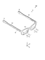
- FIG. 1 is a perspective view of electronic glasses according to Embodiment 1 of the present invention.
- FIG. 2 is a block diagram showing an internal circuit of the electronic glasses.
- 3 is a cross-sectional view taken along line AA in FIG.
- FIG. 4 is a front view of the lens.
- FIG. 5 is a flowchart of the lens manufacturing method according to the first embodiment.
- FIG. 5A is a cross-sectional view of the intermediate assembly for explaining the process of step S110 shown in FIG.
- FIG. 6 is a front view of a semi-finished lens according to Embodiment 2 of the present invention.
- 7 is a cross-sectional view taken along line BB in FIG.
- FIG. 8A is a cross-sectional view for explaining a first step in the method of manufacturing a semifinished lens.
- FIG. 8B is a cross-sectional view for explaining a second step in the method of manufacturing a semifinished lens.
- FIG. 8C is a cross-sectional view for explaining a third step in the method of manufacturing a semifinished lens.
- FIG. 8D is a cross-sectional view for explaining a fourth step in the method of manufacturing a semifinished lens.
- FIG. 8E is a cross-sectional view for explaining a fifth step in the method of manufacturing a semifinished lens.
- FIG. 8F is a cross-sectional view for explaining a sixth step in the method of manufacturing a semifinished lens.
- FIG. 9 is a cross-sectional view of a lens according to the second embodiment.
- FIG. 10 is a flowchart of a method for manufacturing a semi-finished lens according to the second embodiment.
- Embodiment 1 The electronic glasses 100 according to Embodiment 1 of the present invention will be described with reference to FIGS.
- FIG. 1 is a perspective view illustrating an example of the configuration of the electronic glasses 100 according to the present embodiment.
- FIG. 2 is a block diagram showing an internal circuit of the electronic glasses 100.
- the electronic glasses 100 includes a frame 10, a pair of lenses 11, a control unit 13, a detection unit 14, and a pair of power supplies 15.
- the frame 10 has a front 101 and a pair of temples 102.
- the portion where the front 101 is arranged is referred to as the front (front) of the electronic glasses 100.
- the pair of temples 102 holds the control unit 13, the detection unit 14, and the pair of power sources 15. Note that only one of the pair of power supplies 15 may be used. In this case, the power supply 15 is held only in one of the pair of temples 102 (for example, the right temple 102).
- a user (wearer) of the electronic glasses 100 switches the optical characteristic (for example, transmittance) of the liquid crystal lens unit 11 a of the lens 11 by operating (for example, touching) the detection unit 14 provided on the temple 102. .
- the control unit 13 switches between a state where a voltage is applied to the liquid crystal lens unit 11a and a state where no voltage is applied based on the operation.
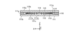
- ⁇ About the lens> 3 is a cross-sectional view taken along line AA in FIG.
- FIG. 4 shows the lens 11 arranged on the left side when the electronic glasses 100 are viewed from the front.
- an orthogonal coordinate system (X, Y, Z) is used for convenience of explanation.
- the orthogonal coordinate system (X, Y, Z) shown in each figure is a common orthogonal coordinate system.
- the X direction coincides with the left and right direction of the user when the eyewear is worn by the user (hereinafter simply referred to as “wearing state”).
- the Y direction coincides with the vertical direction of the user in the mounted state.
- the Z direction coincides with the front-rear direction of the user and the direction of the optical axis of the lens 11 in the mounted state.
- thickness direction means the thickness direction of the lens 11 without particular notice.
- the thickness direction coincides with the Z direction of the orthogonal coordinate system described above.
- each member is a surface on the side far from the user (Z direction + side) in the mounted state.
- the “back surface” of each member is a surface closer to the user (Z direction-side) in the mounted state.
- the lens 11 is curved in a convex shape toward the Z direction + side.
- the curvature of the lens 11 is shown as zero.
- the pair of lenses 11 are formed so as to be symmetric when the electronic glasses 100 are viewed from the front, and have the same components. Therefore, in the following description, the lens 11 for the right eye of the electronic glasses 100 will be described, and the description of the lens 11 for the left eye will be omitted.
- the lens 11 has a liquid crystal lens part 11a and a normal lens part 11b which is a part other than the liquid crystal lens part 11a.
- the liquid crystal lens unit 11a can switch its focal length (frequency) by voltage. As shown in FIG. 3, the liquid crystal lens unit 11a includes a first substrate 111, a first electrode 112, a liquid crystal layer 113, a second electrode 114, and a second substrate 115 in order from the rear side (Z direction-side). Have.
- the first electrode 112, the liquid crystal layer 113, and the second electrode 114 constitute an electric element.
- the normal lens portion 11b includes a first substrate 111, a first electrode 112, an adhesive layer 116, a second electrode 114, and a second substrate 115 in order from the rear side.
- the liquid crystal lens unit 11a and the normal lens unit 11b share the first substrate 111, the first electrode 112, the second electrode 114, and the second substrate 115.
- the components of the liquid crystal lens unit 11a and the normal lens unit 11b are each translucent to visible light.
- the first substrate 111 has a plate shape that curves in a convex shape toward the Z direction + side (upper side in FIG. 3).
- the surface 111a of the first substrate 111 is a convex curved surface that curves in a convex shape toward the Z direction + side.
- the back surface 111b of the first substrate 111 is a concave curved surface that curves in a concave shape toward the Z direction + side.
- the thickness dimension of the first substrate 111 in the direction of the optical axis of the lens 11 varies depending on the location.
- the first substrate 111 in the case of a lens for correcting myopia (also referred to as a minus lens), the first substrate 111 has the largest thickness dimension at the outer periphery.
- the first substrate 111 In the case of a lens for hyperopia correction (also referred to as a plus lens), the first substrate 111 has the smallest thickness dimension at the outer periphery.
- the first substrate 111 may have the same thickness dimension in the direction of the optical axis of the lens 11 throughout.
- each of the front surface 111a and the back surface 111b may be a spherical surface having a single curvature or a complex curved surface having a plurality of curvatures. Further, at least one of the front surface 111a and the back surface 111b may be a flat surface.
- the first substrate 111 has a diffraction region 111c in a portion corresponding to the liquid crystal lens portion 11a of the surface 111a.
- the diffractive region 111c includes a hemispherical convex portion 111d disposed in the central portion, and a plurality of annular first convex strips 111e disposed on a concentric circle with the convex portion 111d as the center.
- Examples of the shape of the convex portion 111d and the first convex strip 111e include a Fresnel lens shape.
- a part of convex part 111d and the 1st convex strip 111e may be a Fresnel lens shape, and all may be a Fresnel lens shape.
- the first substrate 111 is made of inorganic glass or organic glass.
- the first substrate 111 is preferably made of organic glass.
- the organic glass is a thermosetting material made of thermosetting polyurethanes, polythiourethanes, polyepoxides, or polyepisulfides, or a thermoplastic material made of poly (meth) acrylates, or a copolymer thereof or Any of thermosetting (cross-linked) materials consisting of a mixture.
- substrate 111 is not limited to these, The well-known material used as a material of a lens can be employ
- the refractive index of the first substrate 111 and the second substrate 115 is high.
- the refractive indexes of the first substrate 111 and the second substrate 115 are preferably 1.55 or more, and more preferably 1.65 or more.
- the first electrode 112 and the second electrode 114 are a pair of transparent electrodes having translucency.
- the first electrode 112 is disposed between the first substrate 111 and the liquid crystal layer 113.
- the second electrode 114 is disposed between the liquid crystal layer 113 and the second substrate 115.
- the first electrode 112 and the second electrode 114 may be disposed over at least a range (liquid crystal lens portion 11a) in which a voltage can be applied to the liquid crystal layer 113.
- the material of the first electrode 112 and the second electrode 114 is not particularly limited as long as the material has the desired translucency and conductivity.
- Examples of the first electrode 112 and the second electrode 114 include indium tin oxide (ITO) and zinc oxide (ZnO).
- the materials of the first electrode 112 and the second electrode 114 may be the same as or different from each other.
- the liquid crystal layer 113 is disposed between the first electrode 112 and the second electrode 114.
- the liquid crystal layer 113 is configured such that its refractive index changes depending on whether or not a voltage is applied.
- the refractive index of the liquid crystal layer 113 is adjusted to be substantially the same as the refractive index of the first substrate 111 and the refractive index of the second substrate 115 in a state where no voltage is applied to the liquid crystal layer 113.
- the refractive index of the liquid crystal layer 113 is adjusted to be different from the refractive index of the first substrate 111 and the refractive index of the second substrate 115 when a voltage is applied to the liquid crystal layer 113.
- the liquid crystal layer 113 contains a liquid crystal material.
- the alignment state of the liquid crystal material when a voltage is applied is different from the alignment state of the liquid crystal material when a voltage is not applied.
- the liquid crystal material can be appropriately selected according to the refractive index of the first substrate 111 and the refractive index of the second substrate 115.
- the liquid crystal material can be composed of cholesteric liquid crystal, nematic liquid crystal, or the like.
- the second substrate 115 is disposed in front of the first substrate 111 so as to face the surface 111 a of the first substrate 111.
- the second substrate 115 has a plate shape that curves convexly toward the front side.
- the surface 115a of the second substrate 115 is a convex curved surface that curves in a convex shape toward the Z direction + side.
- the back surface 115b of the first substrate 111 is a concave curved surface that curves concavely toward the Z direction + side.
- the second substrate 115 has the same thickness dimension in the direction of the optical axis of the lens 11 throughout.
- that the thickness dimension in the direction of the optical axis of the second substrate 115 is equal may include an error ( ⁇ 0.1 W) of ⁇ 10%.
- the second substrate 115 may have a different thickness dimension in the direction of the optical axis of the lens 11 depending on the location.
- each of the front surface 115a and the back surface 115b may be a spherical surface having a single curvature or a complex curved surface having a plurality of curvatures.
- at least one of the front surface 115a and the back surface 115b may be a flat surface.
- the second substrate 115 is different from the first substrate 111 in transmittance for light in a predetermined wavelength range. Therefore, the second substrate 115 includes an additive that the first substrate 111 does not have.
- the base material of the second substrate 115 is the same as that of the first substrate 111.
- the refractive index (second refractive index) of the second substrate 115 is equal to the refractive index (first refractive index) of the first substrate 111.
- that the first refractive index and the second refractive index are equal may include a range where the difference between the first refractive index and the second refractive index is ⁇ 0.1.
- a photochromic compound a selective absorber that selectively absorbs ultraviolet rays (hereinafter referred to as “ultraviolet absorber”), high energy visible light (short wavelength dimming of 400 to 500 nm, particularly 400 to 420 nm).
- ultraviolet absorber a selective absorber that selectively absorbs blue light
- blue selective absorber a selective absorber that selectively absorbs blue light
- rare earth metal compound for example, a neodymium compound
- an organic dye for example, a porphyrin compound
- Lenses with added photochromic compounds function as transparent lenses indoors, and in the outdoors they respond to sunlight (ultraviolet rays), causing the lenses to turn gray, brown, etc., and protect the eyes from glare. .
- the state where the lens to which the photochromic compound is added is not colored is sometimes referred to as the normal state of the second substrate.
- the state in which the lens to which the photochromic compound is added is colored is sometimes referred to as the colored state of the second substrate.
- the spectacles having such a lens are highly functional spectacles that can be used both indoors and outdoors, and in recent years, the demand thereof has been increasing.
- photochromic compounds can be used.
- photochromic compounds International Publication No. 2012/141306, Japanese Patent Application Laid-Open No. 2004-78052, International Publication No. 2014/208994, Japanese Patent Application Laid-Open No. 8-27236, Japanese Patent Application Laid-Open No. 2005-23238, and And photochromic compounds described in JP-A-2008-30439.
- photochromic compound one or more of spiropyran compounds, chromene compounds, spirooxazine compounds, fulgide compounds, and bisimidazole compounds are mixed depending on the desired coloration. Photochromic compounds.
- the photochromic compound can be synthesized by a known method. For example, the methods described in JP-T-2004-500319, International Publication No. 2009/146509, International Publication No. 2010/20770, International Publication No. 2012/149599, and International Publication No. 2012/162725 Is obtained.
- a lens to which an ultraviolet absorber is added can protect the eyes from damage caused by ultraviolet rays.
- ultraviolet rays having a wavelength of 400 nm or less are known to have an adverse effect on the cornea and the crystalline lens, and a lens capable of effectively absorbing such ultraviolet rays is required.
- iso (thio) cyanate or polythiol which is a polyurethane resin material
- isooctyl-3- (3- (2H-benzotriazol-2-yl) -5-tert-butyl-4-hydroxyphenylpropionate
- 2- [ A polyurethane resin is produced by adding a benzotriazole ultraviolet absorber such as 2-hydroxy-3,5-bis (dimethylbenzyl) phenyl] -2H-benzotriazole, which reduces the optical properties.
- the ultraviolet absorber is 2- [2-hydroxy-3- (dimethylbenzyl) -5- (1,1,3,3-tetramethylbutyl) phenyl] -2H-benzotriazole, isooctyl-3- (3 -(2H-benzotriazol-2-yl) -5-t-butyl-4-hydroxyphenylpropionate, 2- (3,5-di-t-butyl-2-hydroxyphenyl) benzotriazole, 2- (3 , 5-di-t-pentyl-2-hydroxyphenyl) benzotriazole, 2- [2-hydroxy-3,5-bis (dimethylbenzyl) phenyl] -2H-benzotriazole, and 2- (3,5- It is preferably at least one selected from the group consisting of di-t-butyl-2-hydroxyphenyl) -5-chlorobenzotriazole.
- the amount of the ultraviolet absorber added for the purpose of absorbing ultraviolet rays is preferably 0.03 to 1.5 wt%, more preferably 0.05 to 0.5 wt% with respect to the polymerizable composition.
- the ultraviolet absorber when intended for cutting high-energy visible light (intersecting lines having a wavelength in the range of 400 to 420 nm), has a maximum absorption wavelength of 350 nm to 370 nm when dissolved in a chloroform solution.
- a benzotriazole type compound, a benzophenone type compound, or a salicylic acid ester type compound can be used.
- the ultraviolet absorber one or more of these ultraviolet absorbers are preferably used, and two or more different ultraviolet absorbers may be contained.
- the amount of UV absorber added for the purpose of cutting high-energy visible light is 0.3 to 2% by weight, preferably 0.3 to 1.5%, based on the total weight of the resin for optical materials or the polymerizable compound. % By weight, more preferably in the range of 0.3 to 1.2% by weight.
- a test specimen having a composition similar to that of the first substrate 111 and the second substrate 115 containing an ultraviolet absorber and having a thickness of 2 mm is used for light having a wavelength of 440 nm.
- the light transmittance of the specimen is 80% or more, preferably 85% or more, and the light transmittance of the specimen to light having a wavelength of 420 nm is 70% or less, preferably 50% or less, and
- the light transmittance of the test specimen with respect to light having a wavelength of 410 nm is 10% or less, preferably 5% or less.
- the above light transmittance range it is possible to obtain a lens having a high blocking effect against blue light having a wavelength of about 420 nm and being colorless and transparent and having an excellent appearance. Further, by setting the light transmittance for light having a wavelength of 440 nm to 80% or more, a molded body (optical material) that is colorless and transparent and excellent in appearance can be obtained. In addition, you may combine these numerical ranges arbitrarily.
- the lens to which the blue selective absorbent is added can protect the eyes and the like from obstructions caused by high energy visible light (HEV light: light having a wavelength of 400 to 500 nm).
- high-energy visible light reaches the retina and is considered to cause age-related macular degeneration in the long term.
- short-wave dimming with a wavelength of 400 to 420 nm damages retinal cells. Therefore, there is a demand for a lens capable of cutting light in the region of 400 to 420 nm (also referred to as visible light short wavelength region), among high energy visible light.
- Such a lens can reduce damage to retinal cells and reduce the cause of age-related macular degeneration.
- the lens preferably has a light cut rate of about 5% or less with respect to light having a wavelength of 420 nm.
- Rare earth metal compounds increase the contrast and give a clear and glare-proof effect. Since the rare earth metal compound has a very sharp peak shape of the absorption spectrum in the absorption wavelength band in the visible light region, the wavelength region that can be absorbed is narrow. For this reason, the rare earth metal compound can selectively shield light in a wavelength band that easily gives glare. Such rare earth metal compounds have both anti-glare properties and visibility because they can transmit the wavelength bands necessary for visibility and selectively absorb the wavelength bands that adversely affect glare. Lens can be realized. As an example, when a rare earth metal compound that can selectively absorb visible light having a wavelength of about 585 nm is added to the lens, an effective antiglare property can be obtained.
- Such a rare earth metal compound may be a compound containing a rare earth metal ion.
- the rare earth metal ions may be appropriately selected according to the required optical properties (that is, light absorption characteristics). For example, trivalent neodymium ions have absorption peaks near 575 nm and 525 nm in the visible light region. Trivalent erbium ions have an absorption peak in the vicinity of 520 nm. Trivalent praseodymium ions have absorption peaks near 575 nm and 445 nm. Trivalent holmium ions have absorption peaks at around 535 nm and 450 nm. In consideration of such absorption peaks of rare earth metal ions, a rare earth metal suitable for each application may be selected.
- the rare earth metal ion that can be employed in the present embodiment may be selected from neodymium, erbium, praseodymium, holmium, dysprosium, thulium, ytterbium, and lutetium.
- the rare earth metal ion is preferably selected from neodymium, erbium, praseodymium and holmium.
- the rare earth metal ion is more preferably selected from neodymium and erbium.
- Neodymium is most preferred as the rare earth metal ion.
- the rare earth metal ion contained in the rare earth metal compound may be singular or plural.
- neodymium ions may be used alone or in combination with erbium ions.
- the lens to which the neodymium compound is added assists the ability to discriminate between brightness and color differences by selectively cutting yellow light with a wavelength of around 585 nm to reduce glare.
- the lens to which the neodymium compound is added preferably has a cut rate of about 60% with respect to light having a wavelength of around 585 nm.
- the lens to which the neodymium compound is added preferably has a transmittance of 60% or more and 90% or less with respect to light having a wavelength of 580 nm.
- the porphyrin compound has an absorption maximum wavelength in a wavelength region between 440 and 570 nm, and an absorption spectrum measured at an optical path length of 10 mm in a 0.01 g / L toluene solution has a half-width of an absorption peak of 10 nm or more.
- a compound having an absorption maximum wavelength in a wavelength region between 440 and 510 nm, and a compound having an absorption maximum wavelength in a wavelength region between 520 and 570 nm are more preferable.
- the second substrate 115 to which the photochromic compound is added is referred to as a photochromic lens.
- the second substrate 115 to which the blue selective absorbent is added is referred to as a blue light cut lens.
- the second substrate 115 to which the neodymium compound is added is referred to as a neocontrast lens.
- Examples of the method for adding the photochromic compound to the second substrate 115 include coating, dyeing, and kneading.
- the second substrate 115 has a coating layer containing a photochromic compound on at least one of the front surface 115a and the back surface 115b (hereinafter referred to as “coated surface”).
- a coating layer is formed by applying a coating composition to the coated surface and curing it.
- the curing method of the coating composition include a method of photocuring by irradiating light energy rays such as ultraviolet rays or visible light (hereinafter referred to as “photocuring method”), and a method of thermally curing by applying thermal energy. (Hereinafter referred to as “thermosetting method”).
- photocuring method irradiating light energy rays
- thermally curing by applying thermal energy.
- the photochromic compound is added to the second substrate 115 by being immersed in a dyeing liquid heated to a predetermined temperature.
- a dyeing process is preferably performed in a state before the second substrate 115 is fixed to the first substrate 111.
- the second substrate 115 is formed by kneading a photochromic compound into a molten base material, pouring it into a mold and solidifying it. Such a kneading process is naturally performed in a state before the second substrate 115 is fixed to the first substrate 111.
- the second substrate 115 to which the photochromic compound is added has a photochromic function that continuously changes between the transparent coloring state and the transparent state according to the amount of light (ultraviolet rays).
- the second substrate 115 to which a photochromic compound is added (kneaded) suppresses the transmittance with respect to light having a wavelength of 380 nm in a colored state to 8% or less, preferably 5% or less, more preferably 2% or less. it can.
- the photochromic performance (coloring performance) of the second substrate 115 containing a photochromic compound will be described.
- a test body (not shown) having a composition equivalent to that of the second substrate 115 containing a photochromic compound and a thickness of 2.0 mm is made.
- the test specimen is irradiated with ultraviolet rays having a wavelength of 365 nm for 10 minutes from a height of 155 mm.
- a color difference meter (CR-200 manufactured by Konica Minolta Co., Ltd.), the L * value, a * value, and b * value in the hue of the specimen before and after UV irradiation are measured.
- the photochromic performance (coloring performance) of the second substrate 115 containing a photochromic compound is a value obtained by calculating the amount of change in hue from the following formula 1 based on the L * value, a * value, and b * value before and after UV irradiation ( ⁇ E * ab) is preferably 15 or more, and more preferably 20 or more.
- the L * value, a * value, and b * value in the hue of the molded product before irradiation are L 1 *, a 1 *, and b 1 *, respectively.
- the L * value, a * value, and b * value in the hue of the molded article after irradiation are L 2 *, a 2 *, and b 2 *, respectively.
- the photochromic performance (fading performance) of the second substrate 115 containing a photochromic compound will be described.
- a test body (not shown) having a composition equivalent to that of the second substrate 115 containing a photochromic compound and a thickness of 2.0 mm is made.
- the test specimen is irradiated with ultraviolet rays having a wavelength of 365 nm for 10 minutes from a height of 155 mm.
- the color difference meter (CR-200 manufactured by Konica Minolta Co., Ltd.) was used to determine the L * value and a * value in the hue of this specimen. And b * values are measured.
- the photochromic performance (fading performance) of the second substrate 115 containing the photochromic compound was determined by leaving the L 1 * value, a 1 * value, and b 1 * value of the test specimen before UV irradiation, and 10 minutes after UV irradiation.
- the value ( ⁇ E * ab) obtained by calculating the amount of change in hue from Equation 1 is 5 or more and less than 10 Preferably, it is less than 5.
- ⁇ a * is a 3 * and a 1 *
- examples of the method of adding the blue selective absorbent to the second substrate 115 include coating and kneading.
- the blue selective absorbent has a function of selectively absorbing light in a wavelength range of 380 nm to 500 nm.
- the second substrate 115 has a coating layer containing a blue selective absorbent on at least one of the front surface 115a and the back surface 115b.
- a coating layer is formed by applying a coating composition to the coated surface and curing it.
- the curing method of the coating composition is the same as that for the photochromic compound.
- Such a coating process is performed before the second substrate 115 is fixed to the first substrate 111.
- the second substrate 115 is formed by kneading a blue selective absorbent into a molten base material, pouring it into a mold and hardening (for example, by injection molding). Such a kneading process is naturally performed in a state before the second substrate 115 is fixed to the first substrate 111.
- a method for measuring the blue light cut rate of the second substrate 115 containing the blue selective absorbent will be described. First, a test body that is a 2 mm thick planar lens or a 2 mm thick resin flat plate is prepared. Next, the absorption spectrum of the specimen is measured with a UV-VIS spectrometer manufactured by JASCO Corporation. And the blue light cut rate of a test body is calculated. The blue light cut rate is a value obtained by subtracting the average transmittance of the test specimen for light having a wavelength of 380 to 500 nm from 100.
- a method for measuring the light transmittance of the second substrate 115 containing the blue selective absorbent will be described.
- a test body which is a planar lens having a thickness of 2 mm or a resin flat plate having a thickness of 2 mm is prepared.
- an absorption spectrum between 800 nm and 250 nm of the specimen is measured with a UV-VIS spectrometer manufactured by JASCO Corporation, and the transmittance is measured at each wavelength.
- the refractive index and Abbe number of the second substrate 115 containing the blue selective absorbent are measured at 20 ° C. using a Shimadzu Purfrich refractometer KPR-30.
- the second substrate 115 is formed by kneading a neodymium compound into a molten base material, pouring it into a mold and solidifying it. Such a kneading process is naturally performed in a state before the second substrate 115 is fixed to the first substrate 111.
- the step of adding the additive to the second substrate 115 is preferably performed in a state before the second substrate 115 is fixed to the first substrate 111.
- the thickness dimension of the second substrate 115 varies depending on the location, color unevenness occurs in the lens 11 when viewed from the front according to the thickness dimension. Specifically, in the second substrate 115, the color of the portion with the large thickness dimension becomes dark and the color of the portion with the small thickness dimension becomes light. On the other hand, when the thickness dimension of the second substrate 115 is the same throughout, the color unevenness of the lens 11 is less likely to occur when viewed from the front.
- an additive is not limited to the above-mentioned additive.
- various additives that can make the transmittance of the second substrate 115 different from the transmittance of the first substrate 111 with respect to light in a predetermined wavelength range can be selected.
- the coating layer may have a multilayer structure including a plurality of types of layers. That is, the second substrate 115 may have a plurality of coating layers selected from a coating layer containing a photochromic compound, a coating layer containing a blue selective absorbent, and a coating layer containing a neodymium compound.
- the adhesive layer 116 is disposed between the first substrate 111 and the second substrate 115 in the normal lens portion 11b, and bonds the first substrate 111 and the second substrate 115 together.
- the adhesive layer 116 is disposed between the first electrode 112 and the second electrode 114.
- the adhesive layer 116 also has a function of sealing a liquid crystal material included in the liquid crystal layer 113.
- the adhesive layer 116 is composed of a cured adhesive.
- the material of the adhesive is not particularly limited as long as it has translucency and can appropriately bond the first substrate 111 and the second substrate 115. From the viewpoint of adjusting the optical power of the lens 11, an adhesive having a desired refractive index can be selected.
- the adhesive constituting the adhesive layer 116 is preferably an adhesive that is photocured by irradiation with light energy rays such as ultraviolet rays or visible rays. Since such an adhesive does not apply heat to the first substrate 111, the second substrate 115, and the liquid crystal lens portion 11a when cured, it is effective in preventing deformation or damage of these members.
- the lens 11 may further include another component having translucency as necessary.
- the other constituent elements include an insulating layer and an alignment film.
- the insulating layer prevents conduction between the first electrode 112 and the second electrode 114.
- the insulating layers are disposed between the first electrode 112 and the liquid crystal layer 113 and between the liquid crystal layer 113 and the second electrode 114, respectively.
- the material of the insulating layer a known material used as a light-transmitting insulating layer can be used.
- An example of the material for the insulating layer is silicon dioxide.
- the alignment film controls the alignment state of the liquid crystal material in the liquid crystal layer 113.
- the alignment films are disposed between the first electrode 112 and the liquid crystal layer 113 and between the liquid crystal layer 113 and the second electrode 114, respectively.
- a material of the alignment film a known material used as an alignment film of a liquid crystal material can be used.
- An example of the material of the alignment film includes polyimide.
- the lens 11 is manufactured by the following manufacturing method, for example.
- a method for manufacturing the lens 11 according to the present embodiment will be described with reference to FIG.
- the operator prepares the first substrate 111.
- the first substrate 111 is manufactured by a known method such as injection molding.
- the outer shape of the first substrate 111 in plan view is processed to be the same shape as the outer shape of the lens 11 in plan view.
- the first substrate 111 is a common component in the lens 11 incorporated in the frame having the same structure. Therefore, the first substrate 111 is manufactured by a common manufacturing method.
- the operator prepares the second substrate 115.
- a second substrate 115 is also manufactured by a known method such as injection molding.
- the second substrate 115 is a non-common component that can be selected according to desired optical characteristics in the lens 11 incorporated in the frame having the same structure. That is, for the second substrate 115, a plurality of types of second substrates 115 having different transmittances with respect to light in a predetermined wavelength range from the first substrate 111 are manufactured.
- the additive When the additive is added by coating or dyeing, the intermediate lens produced by injection molding is coated or dyed. Moreover, when the addition method of an additive is kneading, an additive is added with respect to the molten base material used by injection molding before injection molding.
- the operator selects a second substrate 115 having desired optical characteristics from among a plurality of types of second substrates 115 having different optical characteristics such as a photochromic lens, a blue light cut lens, and a neo-contrast lens.
- step S ⁇ b> 103 of FIG. 5 the worker provides the first electrode 112 on the first substrate 111.
- step S ⁇ b> 104 of FIG. 5 the worker provides the second electrode 114 on the second substrate 115.
- a method of providing the first electrode 112 on the first substrate 111 and a method of providing the second electrode 114 on the second substrate 115 include a vacuum deposition method and a sputtering method. Such a method is preferably performed at a temperature not higher than the glass transition point “Tg” of the members (that is, the first substrate 111 and the second substrate 115) on which the electrodes are provided.
- step S105 of FIG. 5 the operator places a liquid crystal material on the diffraction region 111c of the first substrate 111 on which the first electrode 112 is provided, and at the same time, the diffraction region 111c on the surface 111a of the first substrate 111.
- an adhesive agent is arrange
- the preliminary region 111f is formed in consideration of the adhesive application pattern and application amount, the final thickness of the adhesive layer, the size and shape of the diffraction region 111c, the degree of pressure reduction (step S107 described later), and the like.
- the adhesive is composed of a plurality of adhesive elements.
- Each adhesive element has a ball shape, and is supplied to the surface 111a of the first substrate 111 by a jet dispenser (not shown). Adjacent adhesive elements do not contact each other.
- step S106 in FIG. 5 the operator places the first substrate 111 on which the liquid crystal material and the adhesive are arranged in the internal space of the sealed container (not shown).
- the first substrate 111 is fixed to the sealed container by a fixing member (not shown).
- step S106 of FIG. 5 the operator places the second substrate 115 provided with the second electrode 114 in the internal space of the sealed container.
- the second substrate 115 is fixed to the sealed container by a fixing member (not shown). Further, the second substrate 115 faces the first substrate 111 with a predetermined gap.
- step S107 of FIG. 5 the atmospheric pressure in the internal space in which the first substrate 111 and the second substrate 115 are arranged is reduced to an atmospheric pressure lower than the atmospheric pressure by a vacuum pump.
- the process of step S107 in FIG. 5 is called a decompression process.
- step S ⁇ b> 108 of FIG. 5 the first substrate 111 is moved so as to approach the second substrate 115.
- the means for moving the first substrate 111 may be manual or automatic.
- step S108 the second substrate 115 may be moved closer to the first substrate 111.
- step S108 when the front surface 111a of the first substrate 111 is in contact with the back surface 115b of the second substrate 115, the fixation of the second substrate 115 is released. Then, the back surface 115 b of the second substrate 115 is pressed against the front surface 111 a of the first substrate 111 by the weight of the second substrate 115. In this way, the first substrate 111 and the second substrate 115 are bonded together.
- the process of step S108 in FIG. 5 is called a bonding process.
- step S109 of FIG. 5 the first substrate 111 and the second substrate 115 are held for a predetermined time in a state of being bonded to each other. Then, the adhesive elements disposed so as to be adjacent to each other between the first substrate 111 and the second substrate 115 are pressed and connected by the second substrate 115. As a result, the adhesive is disposed so as to surround the periphery of the diffraction region 111c.
- a spare space 111g (see FIG. 5A) is formed between the spare region 111f of the first substrate 111 and the back surface 115b of the second substrate 115.
- the preliminary space 111g and the diffraction region 111c are isolated from the external space by an adhesive.
- the process of step S109 in FIG. 5 is called a standby process.
- the spare space 111g Easy to form.
- step S110 of FIG. 5 the atmospheric pressure in the sealed container is restored to atmospheric pressure.
- the adhesive is drawn toward the spare space 111g. Further, since the adhesive has viscosity, if the flow-in speed cannot catch up with the return pressure speed, the reserve space 111g has a negative pressure.
- step S110 in FIG. 5 is referred to as a decompression process.
- the application amount of the liquid crystal material is set to such an amount that the liquid crystal material is held on the diffraction region 111c by the surface tension in the second substrate 115 in the stage of the decompression process. For this reason, only the adhesive is drawn into the spare space 111g, and the liquid crystal material is not drawn. That is, since the adhesive and the liquid crystal material are not mixed, the adhesive strength in the adhesive layer can be increased.
- step S111 in FIG. 5 the operator cures the adhesive.
- the lens 11 is manufactured by the above process.
- the method for curing the adhesive is as described above.
- the adhesive is cured by irradiating light from the rear surface side of the first substrate 111. This is because if the light is irradiated from the front side, that is, the front side of the second substrate 115, the second substrate 115, which is a photochromic lens, absorbs the light and does not cure.
- step S111 heat at a temperature higher than the glass transition point “Tg” of the first substrate 111 and the second substrate 115 is applied to the constituent members of the lens 11. There is nothing.
- the processing performed in steps S106 to S111 in FIG. 5 as described above is called vacuum bonding.
- the adhesive may be disposed on a portion of the second substrate 115 facing the portion other than the diffraction region 111c of the first substrate 111.
- the order of the above-described steps S101 to S111 is appropriately changed within a technically consistent range. Further, the above-described steps S101 to S111 may be performed in parallel as long as there is no technical contradiction.
- the subject that performs the above-described manufacturing method is not limited to a person but may be a machine. Further, if necessary, after step S111 in FIG. 5, at least one of the front surface and the back surface of the lens 11 may be subjected to post-processing such as coating processing, cutting processing, grinding processing, or polishing processing.
- the lens 11 having optical characteristics corresponding to the user's application can be provided by changing the additive that the second substrate 115 has.
- a production process for example, a coating process
- a production process is required after the bonding process, so that production is possible.
- Efficiency can be reduced.
- a production process for example, a coating process
- a plurality of types of second substrates 115 having special optical characteristics and the first substrate 111 that is a common component are used before the first substrate 111 and the second substrate 115 are bonded together. And can be prepared. Then, a second substrate 115 having desired optical characteristics is selected from a plurality of types of second substrates 115 and bonded to the first substrate 111. That is, in the present embodiment, the step of imparting optical characteristics to the second substrate 115 is not performed after the bonding step.
- Such a configuration of the present embodiment is effective in improving the production efficiency (that is, shortening the manufacturing time) as compared with the case where special optical characteristics are imparted to the bonded lenses.
- the thickness dimension of the second substrate 115 is the same throughout. For this reason, even when the additive is added by kneading, color unevenness hardly occurs in the second substrate 115. Therefore, color unevenness hardly occurs in the lens 11 when viewed from the front.
- the step of adding the additive to the second substrate 115 is performed before the second substrate 115 is fixed to the first substrate 111. For this reason, even when heat is applied to the second substrate 115 in the step of adding the additive, heat is not applied to the first substrate 111 and the liquid crystal layer 113.
- Such a configuration of the present embodiment is effective for preventing deformation or damage of the first substrate 111 and the liquid crystal layer 113.
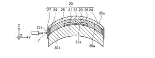
- FIG. 6 is a front view of the semi-finished lens 20.
- 7 is a cross-sectional view taken along line BB in FIG.
- the semi-finished lens 20 is processed into the lens 11 of the first embodiment described above by post-processing. Such a semi-finished lens 20 is also an object of the present invention.
- the semi-finished lens 20 includes a first intermediate substrate 21, a first adhesive layer 22, a film element 23, a spacer member 24, a second intermediate substrate 25, a second intermediate adhesive layer 26, and a fixing member 27.
- the first intermediate substrate 21 (also referred to as a first substrate) will be described with reference to FIG.
- the first intermediate substrate 21 is an optical element made of a transparent plate member having a front surface 21a and a back surface 21b.
- the first intermediate substrate 21 has a disk shape that curves convexly toward the Z direction + side.
- the surface 21a of the first intermediate substrate 21 is a convex curved surface that curves in a convex shape toward the Z direction + side.
- the back surface 21b of the first intermediate substrate 21 is a concave curved surface that is concavely curved toward the Z direction + side.
- the surface 21a is finished to an optical surface by finishing.
- the back surface 21b is an unfinished surface that has not been finished. Such a back surface 21b is finished into an optical surface by post-processing.
- the surface 21a is a spherical surface having a single curvature.
- the back surface 21b is also a spherical surface having a single curvature.
- the back surface 21b is processed into a shape according to the user's visual acuity, for example, by post-processing.
- At least one surface of the front surface 21a and the back surface 21b may be a complex curved surface having a plurality of curvatures. Further, at least one of the front surface 21a and the back surface 21b may be a flat surface.
- the material of the first intermediate substrate 21 is the same as the material of the first substrate 111 of the first embodiment described above.
- the first adhesive layer 22 will be described with reference to FIG.
- the first adhesive layer 22 is disposed between the front surface 21 a of the first intermediate substrate 21 and the back surface of the film element 23, and fixes the film element 23 and the first intermediate substrate 21.
- Such a first adhesive layer 22 is a sheet-like member whose outer shape is substantially the same as that of a film element 23 described later. In a state of being fixed to the first intermediate substrate 21, the first adhesive layer 22 is curved in a convex shape toward the Z direction + side.
- the first adhesive layer 22 is made of, for example, a film-like adhesive made of an optical pressure-sensitive adhesive, a thermosetting adhesive, or an ultraviolet curable adhesive.
- the structure of the film element 23 will be described with reference to FIG.
- the film element 23 (also referred to as an electric element) is a film-like optical element whose optical characteristics are changed by electrical control.
- Such a film element 23 is fixed to the surface 21 a of the first intermediate substrate 21 via the first adhesive layer 22.
- the film element 23 In a state of being fixed to the first intermediate substrate 21, the film element 23 is curved in a convex shape toward the Z direction + side along the surface 21 a of the first intermediate substrate 21.
- the film element 23 is a laminate in which an inner first electrode, a liquid crystal layer, and an inner second electrode are arranged in order from the first film side between the first film member and the second film member. Structure.
- the inner first electrode and the inner second electrode correspond to the first electrode 112 and the second electrode 114 of the first embodiment described above.
- the liquid crystal layer corresponds to the liquid crystal layer 113 of the first embodiment.
- the peripheral edges of the first film member and the second film member are fixed by an adhesive layer.
- the adhesive layer fixes the first film member and the second film member, and also has a function of sealing the liquid crystal material constituting the liquid crystal layer.
- the spacer member 24 will be described with reference to FIG.
- the spacer member 24 is provided between the first intermediate substrate 21 and the second intermediate substrate 25 so that the first intermediate substrate 21 and the second intermediate substrate 25 are closer than the thickness dimension of the spacer member 24. To prevent.
- Such spacer members 24 are arranged at a plurality of locations (three locations in the present embodiment) on the outer peripheral edge of the surface 21a of the first intermediate substrate 21.
- the spacer members 24 are preferably arranged at equal intervals (for example, at intervals of 120 degrees) in the direction along the outer peripheral edge of the first intermediate substrate 21.
- the spacer member 24 is a columnar member and has a predetermined thickness dimension.
- One end portion (end portion on the Z direction + side) of the spacer member 24 is fixed to the back surface 25b of the second intermediate substrate 25 with, for example, an adhesive.
- the other end portion (the end portion on the Z direction side) of the spacer member 24 is fixed to the surface 21a of the first intermediate substrate 21 with, for example, an adhesive.
- the second intermediate adhesive layer 26 is disposed between the first intermediate substrate 21 and the second intermediate substrate 25.
- a space 201 is formed.
- the thickness dimension of the space 201 is equal to the thickness dimension of the spacer member 24. Further, the thickness dimension of the space 201 is larger than the thickness dimension of the film element 23.
- the spacer member 24 as described above is removed in post-processing (specifically, peripheral processing).
- the spacer member may be a partial cylindrical shape having a discontinuous portion at one place in the circumferential direction.
- the discontinuous part is a supply port for supplying a curable composition constituting the second intermediate adhesive layer 26 described later to the space 201.
- the spacer member may be a cylindrical shape that is continuous over the entire circumference.
- Such a cylindrical spacer member has a through-hole or notch penetrating from the inner peripheral surface to the outer peripheral surface in at least one place in the circumferential direction.
- the through hole and the notch are supply ports for supplying the space 201 with the curable composition constituting the second intermediate adhesive layer 26.
- the second intermediate substrate 25 (also referred to as a second substrate) will be described with reference to FIG.
- the second intermediate substrate 25 is disposed on the Z direction + side from the film element 23 and covers the film element 23 via the second intermediate adhesive layer 26.
- Such a second intermediate substrate 25 is an optical element made of a transparent plate member. Specifically, the second intermediate substrate 25 has a disk shape that curves convexly toward the Z direction + side.
- the surface 25a of the second intermediate substrate 25 is a convex curved surface that curves in a convex shape toward the Z direction + side.
- the back surface 25b of the second intermediate substrate 25 is a concave curved surface that is concavely curved toward the Z direction + side.
- the front surface 25a and the back surface 25b are finished to optical surfaces by finishing.
- the surface 25a is a spherical surface having a single curvature.
- the back surface 25b is also a spherical surface having a single curvature.
- the curvature of the front surface 25a and the curvature of the back surface 25b are in a relationship such that the distance between the front surface 25a and the back surface 25b is constant throughout.
- At least one of the front surface 25a and the back surface 25b may be a complex curved surface having a plurality of curvatures. Further, at least one of the front surface 25a and the back surface 25b may be a flat surface.
- the material of the second intermediate substrate 25 is the same as the material of the second substrate 115 of the first embodiment described above. That is, also in this embodiment, the second intermediate substrate 25 is different from the first intermediate substrate 21 in the transmittance for light in a predetermined wavelength range.
- the second intermediate adhesive layer 26 will be described with reference to FIG.
- the second intermediate adhesive layer 26 is disposed in the space 201 between the first intermediate substrate 21 and the second intermediate substrate 25, and fixes the first intermediate substrate 21 and the second intermediate substrate 25, and the film element 23. Protect from impact.
- the second intermediate adhesive layer 26 is an optical element made of a transparent plate member. Specifically, the second intermediate adhesive layer 26 has a disk shape that curves convexly toward the Z direction + side.
- the surface of the second intermediate adhesive layer 26 is a convex curved surface that curves in a convex shape toward the Z direction + side.
- the back surface of the second intermediate adhesive layer 26 is a concave curved surface that is concavely curved toward the Z direction + side.
- the second intermediate adhesive layer 26 has a recess 26a for disposing the film element 23 on the back surface.
- the second intermediate adhesive layer 26 as described above is formed by injecting a curable composition into the space 201 via a communicating portion 27a of the fixing member 27 described later and curing it.
- the curable composition constituting the second intermediate adhesive layer 26 include various optical adhesives.
- a photocurable adhesive that is photocured by irradiation with light energy rays such as ultraviolet rays or visible rays is preferable.
- the thermosetting type adhesive agent which thermosets by applying a thermal energy is also mentioned.
- Each of these adhesives preferably has a low viscosity.
- the fixing member 27 has, for example, a tape shape and is wound around the outer peripheral surface of the first intermediate substrate 21 and the outer peripheral surface of the second intermediate substrate 25 so as to surround the space 201.
- the fixing member 27 also has a function of fixing the first intermediate substrate 21 and the second intermediate substrate 25.
- Such a fixing member 27 has a communication portion 27a that communicates the space 201 with the external space in at least one place in the circumferential direction.
- step S201 of FIG. 10 the operator attaches the surface of the film-like first adhesive layer 22 to the back surface of the film element 23, thereby making the first assembly M1 (see FIG. 8A).
- the film element 23 and the first adhesive layer 22 are not curved.
- step S202 of FIG. 10 the operator attaches the back surface of the first adhesive layer 22 in the first assembly M1 to the front surface 21a of the first intermediate substrate 21, and then the second assembly M2 (see FIG. 8B). ).
- the first intermediate substrate 21 is manufactured by a known method such as injection molding.
- the outer shape of the first intermediate substrate 21 in plan view is a shape that includes the outer shape of the lens 11 in plan view. That is, the outer shape of the first intermediate substrate 21 in plan view is larger than the outer shape of the lens 11 in plan view.
- the first intermediate substrate 21 is a common component common to the semi-finished lens 20 having the same size. Therefore, the first intermediate substrate 21 is manufactured by a common manufacturing method.
- the operation of attaching the first assembly M1 to the surface 21a of the first intermediate substrate 21 is performed using a jig (not shown).
- the jig has a holding surface capable of holding the first assembly M1.
- the holding surface is pressed against the surface 21a, the holding surface is elastically deformed along the surface 21a.
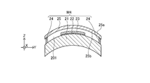
- the film element 23 is attached to the surface 21a while being deformed along the surface 21a.
- step S203 of FIG. 10 the operator arranges the plurality of spacer members 24 around the portion of the surface 21a of the first intermediate substrate 21 where the film element 23 is fixed, and the third assembly M3 ( 8C).
- the third assembly M3 the other end portions (end portions on the Z direction side) of the spacer members 24 are respectively fixed to the surface 21a of the first intermediate substrate 21 with an adhesive, for example.
- step S204 of FIG. 10 the worker arranges the second intermediate substrate 25 on the Z direction + side of the first intermediate substrate 21 to make the fourth assembly M4 (see FIG. 8D).
- the fourth assembly M4 one end portion (end portion on the Z direction + side) of each spacer member 24 is fixed to the back surface 25b of the second intermediate substrate 25 by, for example, an adhesive.
- a space 201 exists between the first intermediate substrate 21 and the second intermediate substrate 25.
- Such a second intermediate substrate 25 is manufactured by a known method such as injection molding.
- the second intermediate substrate 25 is a non-common component that can be selected according to desired optical characteristics in the same size semi-finished lens 20 of the same size. That is, with respect to the second intermediate substrate 25, a plurality of types of second intermediate substrates 25 that are different from the first intermediate substrate 21 in transmittance for light in a predetermined wavelength range are manufactured. The operator selects the second intermediate substrate 25 according to the desired optical characteristics from among them.
- the additive When the additive is added by coating or dyeing, the intermediate lens produced by injection molding is coated or dyed. Moreover, when the addition method of an additive is kneading, an additive is added with respect to the molten base material used by injection molding before injection molding.
- the operator selects the second substrate 115 having desired optical characteristics from among a plurality of types of second intermediate substrates 25 having different optical characteristics, such as a photochromic lens, a blue light cut lens, and a neo-contrast lens.
- step S205 of FIG. 10 the operator winds the fixing member 27 around the outer peripheral surface of the first intermediate substrate 21 and the outer peripheral surface of the second intermediate substrate 25 so as to surround the space 201, and the fifth group A solid M5 (see FIG. 8E) is created.
- the space 201 is closed by a portion other than the communication portion 27a of the fixing member 27. In other words, the space 201 communicates with the external space only through the communication portion 27a.
- step S206 of FIG. 10 the operator can apply the curable composition constituting the second intermediate adhesive layer 26 via the communication portion 27 a of the fixing member 27. Supply to the space 201. And an operator hardens the curable composition in the space 201, and produces the semifinished lens 20 (refer FIG. 7).
- the order of the above-described steps S201 to S206 is appropriately changed within a technically consistent range. Further, the above-described steps S101 to S107 may be performed in parallel as long as there is no technical contradiction.
- the subject that performs the above-described manufacturing method is not limited to a person but may be a machine.
- Each process referring to FIGS. 8A to 8F does not include a process of applying heat.
- Such a semi-finished lens manufacturing method is effective in preventing deformation or damage of the first intermediate substrate 21, the second intermediate substrate 25, and the film element 23.
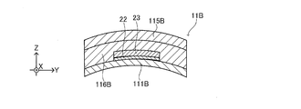
- the semi-finished lens 20 is processed into the lens 11B (see FIG. 9) by post-processing the semi-finished lens 20 obtained by the above manufacturing method. Although a detailed description of the post-processing is omitted, the semi-finished lens 20 is processed into the lens 11 by removing the removal portion 202 (portion surrounded by a two-dot chain line in FIG. 7) by post-processing.
- the semi-finished lens 20 is processed into the lens 11B (see FIG. 9) by post-processing the semi-finished lens 20 obtained by the above manufacturing method. Although a detailed description of the post-processing is omitted, the semi-finished lens 20 is processed into the lens 11 by removing the removal portion 202 (portion surrounded by a two-dot chain line in FIG. 7) by post-processing.
- the first intermediate substrate 21 of the semi-finished lens 20 becomes the first substrate 111B of the lens 11B after being subjected to post-processing.
- the second intermediate substrate 25 of the semi-finished lens 20 becomes the second substrate 115B of the lens 11B after being subjected to post-processing.
- the second intermediate adhesive layer 26 of the semi-finished lens 20 becomes the adhesive layer 116B of the lens 11B.
- the spacer member 24 and the fixing member 27 of the semi-finished lens 20 are removed by post-processing.
- the post-processing includes a back surface processing for grinding the back surface of the semi-finished lens 20 by grinding and a peripheral processing for cutting the outer periphery of the semi-finished lens 20 by cutting processing and polishing processing.
- a coating process for forming a coating layer may be performed on the back surface of the semi-finished lens 20 after the back surface processing (the back surface of the second intermediate substrate 25). Moreover, you may perform the coating process which forms a coating layer in the surface (surface 21a of the 1st intermediate substrate 21) of the semifinished lens 20 at an appropriate timing.
- the coating layer includes, for example, at least one layer of a primer layer, a hard coat layer, an antireflection film layer, an antifogging coat layer, an antifouling layer, and a water repellent layer.
- the coating layer may have a multilayer structure composed of a plurality of types of layers.
- the surface side coating layer may have a single layer structure composed of one kind of layer.
- the coating process for forming such a coating layer is preferably a process in which heat is not applied to the semi-finished lens 20.
- the material of the second intermediate substrate 25 containing an additive for imparting special optical characteristics is more expensive than the material of the first intermediate substrate 21 not containing an additive.
- the volume of the second intermediate substrate 25 occupying the semi-finished lens 20 is smaller than the volume of the first intermediate substrate 21. That is, the material of the second intermediate substrate 25 used for the semifinished lens 20 is less than the material of the first intermediate substrate 21. Therefore, the configuration of the present embodiment can reduce the cost of the semi-finished lens 20 and the lens 11 as compared with the configuration in which the additive is added to the first intermediate substrate 21.
- the proportion of the second intermediate substrate 25 in the removal portion 202 (the portion surrounded by the two-dot chain line in FIG. 7) removed from the semi-finished lens 20 in the post-processing described above is larger than that of the first intermediate substrate 21. small. That is, the amount removed by post-processing is smaller in the second intermediate substrate 25 than in the first intermediate substrate 21.
- the structure of this embodiment can make the yield regarding the material containing an additive high compared with the structure which adds an additive to the material of the 1st intermediate substrate 21.
- FIG. Also from such a viewpoint, the configuration of the present embodiment is advantageous in reducing the cost of the semi-finished lens 20 and the lens 11.
- the step of adding the additive to the second intermediate substrate 25 is performed before the second intermediate substrate 25 is fixed to the first intermediate substrate 21. For this reason, in the step of adding the additive, even when heat is applied to the second intermediate substrate 25, heat is not applied to the first intermediate substrate 21 and the film element 23. Furthermore, if a photo-curing adhesive is employed as the second intermediate adhesive layer 26, heat is applied to the first intermediate substrate 21 and the film element 23 in the step of fixing the second intermediate substrate 25 and the first intermediate substrate 21. There is no participation. Such a manufacturing method is effective for preventing deformation or damage of the first intermediate substrate 21 and the film element 23.
- the film element 23 may be fixed to the second intermediate substrate 25.
- the second intermediate substrate 25 is the first substrate
- the first intermediate substrate 21 is the second substrate.
- the eyewear to which the lens according to the present invention can be applied includes glasses (including electronic glasses and sunglasses) and goggles having an auxiliary mechanism for improving the user's visual acuity like a visual acuity correction lens.
- the eyewear to which the lens according to the present invention can be applied includes various devices having a mechanism for presenting information to the user's field of view or eyes (for example, a glasses-type wearable terminal, a head-mounted display, etc.). It is.
- the eyewear to which the lens according to the present invention can be applied only needs to be able to hold an auxiliary mechanism for improving visual acuity or visibility, a mechanism for presenting information, etc. in front of or around the user's eyes.
- the eyewear to which the lens according to the present invention can be applied is not limited to the glasses type that can be worn on both ears, but may be a type that is worn on the head or one ear.
- the eyewear to which the lens according to the present invention can be applied is not limited to eyewear for both eyes, and may be eyewear for one eye.
- the lens according to the present invention is not limited to glasses lenses, but can be applied to various eyewear lenses.
Abstract
La présente invention concerne un verre de lunettes conçu de façon à être pourvu : d'un premier substrat transparent ayant une surface principale ; d'un deuxième substrat disposé face à la surface principale, la transmittance de celui-ci par rapport à la lumière dans une région de longueur d'onde prédéterminée étant différente de celle du premier substrat ; d'un élément électrique dans lequel une caractéristique optique est modifiée par une commande électrique, l'élément électrique étant disposé entre le premier substrat et le deuxième substrat ; et d'une couche adhésive disposée entre le premier substrat et le deuxième substrat.
Priority Applications (4)
| Application Number | Priority Date | Filing Date | Title |
|---|---|---|---|
| US16/968,102 US20210026159A1 (en) | 2018-02-09 | 2019-02-07 | Lens and method for manufacturing lens |
| JP2019570792A JP7123082B2 (ja) | 2018-02-09 | 2019-02-07 | レンズおよびレンズの製造方法 |
| CN201980008031.2A CN111587396B (zh) | 2018-02-09 | 2019-02-07 | 镜片及镜片的制造方法 |
| EP19751411.0A EP3751332A4 (fr) | 2018-02-09 | 2019-02-07 | Verre et procédé de fabrication de verre |
Applications Claiming Priority (2)
| Application Number | Priority Date | Filing Date | Title |
|---|---|---|---|
| JP2018-022153 | 2018-02-09 | ||
| JP2018022153 | 2018-02-09 |
Publications (1)
| Publication Number | Publication Date |
|---|---|
| WO2019156143A1 true WO2019156143A1 (fr) | 2019-08-15 |
Family
ID=67548119
Family Applications (1)
| Application Number | Title | Priority Date | Filing Date |
|---|---|---|---|
| PCT/JP2019/004354 WO2019156143A1 (fr) | 2018-02-09 | 2019-02-07 | Verre et procédé de fabrication de verre |
Country Status (6)
| Country | Link |
|---|---|
| US (1) | US20210026159A1 (fr) |
| EP (1) | EP3751332A4 (fr) |
| JP (1) | JP7123082B2 (fr) |
| CN (1) | CN111587396B (fr) |
| TW (1) | TWI826419B (fr) |
| WO (1) | WO2019156143A1 (fr) |
Families Citing this family (2)
| Publication number | Priority date | Publication date | Assignee | Title |
|---|---|---|---|---|
| TWI812903B (zh) * | 2019-11-29 | 2023-08-21 | 日商旭化成股份有限公司 | 頭戴式顯示器用樹脂透鏡 |
| US11852952B2 (en) * | 2021-10-27 | 2023-12-26 | Sharp Display Technology Corporation | Liquid crystal lens, head mounted display and polarized sunglasses |
Citations (19)
| Publication number | Priority date | Publication date | Assignee | Title |
|---|---|---|---|---|
| JPH08272036A (ja) | 1994-10-17 | 1996-10-18 | Seiko Epson Corp | フォトクロミック組成物およびそれを用いたフォトクロミック樹脂 |
| JP2004500319A (ja) | 1998-09-11 | 2004-01-08 | コーニング ソシエテ アノニム | C5−c6においてアネル化されたナフトピラン、その調製並びにそれらを含有する組成物および(コ)ポリマーマトリクス |
| JP2004078052A (ja) | 2002-08-22 | 2004-03-11 | Nof Corp | フォトクロミック光学材料の製造方法 |
| JP2005023238A (ja) | 2003-07-04 | 2005-01-27 | Tokuyama Corp | フォトクロミック組成物 |
| JP2008030439A (ja) | 2006-06-30 | 2008-02-14 | Hoya Corp | フォトクロミックレンズの製造方法 |
| WO2009146509A1 (fr) | 2008-06-05 | 2009-12-10 | Advanced Polymerik Pty Ltd | Polymère photochromique et composition comprenant un polymère photochromique |
| WO2010020770A1 (fr) | 2008-08-18 | 2010-02-25 | James Robinson Limited | Molécules bi-photochromiques pontées par polydialkylsiloxane |
| WO2011093530A1 (fr) * | 2010-01-29 | 2011-08-04 | シチズンホールディングス株式会社 | Procédé de fabrication de lunettes électroniques et de lentilles à cristaux liquides |
| JP2012155328A (ja) * | 2012-03-15 | 2012-08-16 | Panasonic Corp | 可変焦点レンズ用セミフィニッシュトブランクの製造方法 |
| JP2012522270A (ja) * | 2009-03-25 | 2012-09-20 | ハイ・パフォーマンス・オプティクス・インコーポレイテッド | 特定の青色光波長を選択的にフィルタ除去するフォトクロミック眼科システム |
| WO2012141306A1 (fr) | 2011-04-13 | 2012-10-18 | Hoya株式会社 | Lentille photochromique pour lunettes |
| WO2012149599A1 (fr) | 2011-05-03 | 2012-11-08 | Advanced Polymerik Pty Ltd | Polymère photochrome |
| JP5075080B2 (ja) * | 2008-10-02 | 2012-11-14 | タレックス光学工業株式会社 | 赤外線吸収性眼鏡用レンズ基材 |
| WO2012162725A1 (fr) | 2011-06-03 | 2012-12-06 | Advanced Polymerik Pty Ltd | Polymères photochromes |
| WO2014208994A1 (fr) | 2013-06-24 | 2014-12-31 | 주식회사 케이오씨솔루션 | Composition apte à être polymérisée pour matière optique hautement réfractante, composition photochromique correspondante et procédé de préparation de matière optique hautement réfractante utilisant les compositions |
| JP2015511893A (ja) * | 2012-01-17 | 2015-04-23 | 三井化学株式会社 | 表面起伏を有する可撓性膜および電気活性光学系におけるその使用 |
| JP2015522842A (ja) | 2012-06-14 | 2015-08-06 | 三井化学株式会社 | 電子眼鏡及び製造方法 |
| WO2017047685A1 (fr) * | 2015-09-16 | 2017-03-23 | 三井化学株式会社 | Composition polymérisable pour matériau optique, matériau optique, procédé de production de la composition polymérisable pour matériau optique, et procédé de production du matériau optique |
| JP2018022153A (ja) | 2016-07-21 | 2018-02-08 | 富士フイルム株式会社 | 積層体及び液晶表示装置 |
Family Cites Families (11)
| Publication number | Priority date | Publication date | Assignee | Title |
|---|---|---|---|---|
| US20030210377A1 (en) * | 2001-10-05 | 2003-11-13 | Blum Ronald D. | Hybrid electro-active lens |
| US6986579B2 (en) * | 1999-07-02 | 2006-01-17 | E-Vision, Llc | Method of manufacturing an electro-active lens |
| TWI323254B (en) * | 2004-02-02 | 2010-04-11 | Mgc Filsheet Co Ltd | Light control plastic lens, coated sheet-like light control element for the lens production, and a production method for light control plastic lens |
| US8360574B2 (en) * | 2006-03-20 | 2013-01-29 | High Performance Optics, Inc. | High performance selective light wavelength filtering providing improved contrast sensitivity |
| CN107272223A (zh) * | 2006-11-28 | 2017-10-20 | 高性能光学公司 | 提供改进的对比灵敏度的高性能选择性光波长过滤 |
| US7654667B2 (en) * | 2007-05-10 | 2010-02-02 | Pixeloptics, Inc. | Progressive addition lens operating in combination with a multi-order diffractive optic |
| WO2009079342A1 (fr) * | 2007-12-14 | 2009-06-25 | Pixeloptics Inc. | Lentilles focales multifocales réfractives-diffractives |
| US8523354B2 (en) * | 2008-04-11 | 2013-09-03 | Pixeloptics Inc. | Electro-active diffractive lens and method for making the same |
| JP4955807B1 (ja) * | 2010-12-15 | 2012-06-20 | パナソニック株式会社 | 可変焦点レンズ用セミフィニッシュトブランクの製造方法 |
| KR101776540B1 (ko) * | 2013-08-02 | 2017-09-07 | 미쯔이가가꾸가부시끼가이샤 | 포토크로믹 광학 재료의 제조 방법 |
| CN103499889B (zh) * | 2013-10-15 | 2016-01-13 | 大连东方科脉电子有限公司 | 一种自动防眩目眼镜及其制造方法 |
-
2019
- 2019-02-07 EP EP19751411.0A patent/EP3751332A4/fr active Pending
- 2019-02-07 JP JP2019570792A patent/JP7123082B2/ja active Active
- 2019-02-07 US US16/968,102 patent/US20210026159A1/en active Pending
- 2019-02-07 CN CN201980008031.2A patent/CN111587396B/zh active Active
- 2019-02-07 WO PCT/JP2019/004354 patent/WO2019156143A1/fr unknown
- 2019-02-11 TW TW108104417A patent/TWI826419B/zh active
Patent Citations (19)
| Publication number | Priority date | Publication date | Assignee | Title |
|---|---|---|---|---|
| JPH08272036A (ja) | 1994-10-17 | 1996-10-18 | Seiko Epson Corp | フォトクロミック組成物およびそれを用いたフォトクロミック樹脂 |
| JP2004500319A (ja) | 1998-09-11 | 2004-01-08 | コーニング ソシエテ アノニム | C5−c6においてアネル化されたナフトピラン、その調製並びにそれらを含有する組成物および(コ)ポリマーマトリクス |
| JP2004078052A (ja) | 2002-08-22 | 2004-03-11 | Nof Corp | フォトクロミック光学材料の製造方法 |
| JP2005023238A (ja) | 2003-07-04 | 2005-01-27 | Tokuyama Corp | フォトクロミック組成物 |
| JP2008030439A (ja) | 2006-06-30 | 2008-02-14 | Hoya Corp | フォトクロミックレンズの製造方法 |
| WO2009146509A1 (fr) | 2008-06-05 | 2009-12-10 | Advanced Polymerik Pty Ltd | Polymère photochromique et composition comprenant un polymère photochromique |
| WO2010020770A1 (fr) | 2008-08-18 | 2010-02-25 | James Robinson Limited | Molécules bi-photochromiques pontées par polydialkylsiloxane |
| JP5075080B2 (ja) * | 2008-10-02 | 2012-11-14 | タレックス光学工業株式会社 | 赤外線吸収性眼鏡用レンズ基材 |
| JP2012522270A (ja) * | 2009-03-25 | 2012-09-20 | ハイ・パフォーマンス・オプティクス・インコーポレイテッド | 特定の青色光波長を選択的にフィルタ除去するフォトクロミック眼科システム |
| WO2011093530A1 (fr) * | 2010-01-29 | 2011-08-04 | シチズンホールディングス株式会社 | Procédé de fabrication de lunettes électroniques et de lentilles à cristaux liquides |
| WO2012141306A1 (fr) | 2011-04-13 | 2012-10-18 | Hoya株式会社 | Lentille photochromique pour lunettes |
| WO2012149599A1 (fr) | 2011-05-03 | 2012-11-08 | Advanced Polymerik Pty Ltd | Polymère photochrome |
| WO2012162725A1 (fr) | 2011-06-03 | 2012-12-06 | Advanced Polymerik Pty Ltd | Polymères photochromes |
| JP2015511893A (ja) * | 2012-01-17 | 2015-04-23 | 三井化学株式会社 | 表面起伏を有する可撓性膜および電気活性光学系におけるその使用 |
| JP2012155328A (ja) * | 2012-03-15 | 2012-08-16 | Panasonic Corp | 可変焦点レンズ用セミフィニッシュトブランクの製造方法 |
| JP2015522842A (ja) | 2012-06-14 | 2015-08-06 | 三井化学株式会社 | 電子眼鏡及び製造方法 |
| WO2014208994A1 (fr) | 2013-06-24 | 2014-12-31 | 주식회사 케이오씨솔루션 | Composition apte à être polymérisée pour matière optique hautement réfractante, composition photochromique correspondante et procédé de préparation de matière optique hautement réfractante utilisant les compositions |
| WO2017047685A1 (fr) * | 2015-09-16 | 2017-03-23 | 三井化学株式会社 | Composition polymérisable pour matériau optique, matériau optique, procédé de production de la composition polymérisable pour matériau optique, et procédé de production du matériau optique |
| JP2018022153A (ja) | 2016-07-21 | 2018-02-08 | 富士フイルム株式会社 | 積層体及び液晶表示装置 |
Non-Patent Citations (1)
| Title |
|---|
| See also references of EP3751332A4 |
Also Published As
| Publication number | Publication date |
|---|---|
| CN111587396A (zh) | 2020-08-25 |
| JP7123082B2 (ja) | 2022-08-22 |
| EP3751332A1 (fr) | 2020-12-16 |
| CN111587396B (zh) | 2022-08-05 |
| JPWO2019156143A1 (ja) | 2021-01-28 |
| TWI826419B (zh) | 2023-12-21 |
| TW201937246A (zh) | 2019-09-16 |
| EP3751332A4 (fr) | 2022-02-23 |
| US20210026159A1 (en) | 2021-01-28 |
Similar Documents
| Publication | Publication Date | Title |
|---|---|---|
| US10520756B2 (en) | Laminated mirror lens | |
| TWI413811B (zh) | 光學用途之模製積層物及其製備方法 | |
| EP1370897B1 (fr) | Lunettes polarisées en polymère présenant une résistance aux chocs elevée de haut qualité optique | |
| US10768447B2 (en) | Thermally influenced changeable tint device | |
| WO2012035885A1 (fr) | Lentille de blocage de lumière pour lunettes de protection | |
| JP5075080B2 (ja) | 赤外線吸収性眼鏡用レンズ基材 | |
| ES2897912T3 (es) | Lente polarizada para gafas de elevado índice de refracción | |
| WO2019156143A1 (fr) | Verre et procédé de fabrication de verre | |
| JP2015069045A (ja) | 複合機能性偏光レンズ | |
| US11598978B2 (en) | Optical lens | |
| WO2017099800A1 (fr) | Lunettes à filtres réfléchissants | |
| CN111417892B (zh) | 具有可变透射镜片的眼镜 | |
| WO2018008179A1 (fr) | Matériau de lunettes | |
| US20230204982A1 (en) | Eyewear with chroma enhancement | |
| CN114911099B (zh) | 偏光变色膜片、镜片及眼镜 | |
| JP2019144381A (ja) | セミフィニッシュドレンズ、セミフィニッシュドレンズの製造方法、およびレンズの製造方法 | |
| US20230033949A1 (en) | Eyewear with selective wavelength filtering | |
| CN112219157A (zh) | 颜色增强镜片 | |
| CN116256902A (zh) | 满足焦度矫正的处方的电活性眼科装置、制造方法以及半成品混合镜片的用途 | |
| TW202338402A (zh) | 抗紅外線可變色光學透鏡裝置 | |
| JP2019117390A (ja) | 複合機能性偏光レンズ |
Legal Events
| Date | Code | Title | Description |
|---|---|---|---|
| 121 | Ep: the epo has been informed by wipo that ep was designated in this application |
Ref document number: 19751411 Country of ref document: EP Kind code of ref document: A1 |
|
| ENP | Entry into the national phase |
Ref document number: 2019570792 Country of ref document: JP Kind code of ref document: A |
|
| NENP | Non-entry into the national phase |
Ref country code: DE |
|
| ENP | Entry into the national phase |
Ref document number: 2019751411 Country of ref document: EP Effective date: 20200909 |