WO2019156143A1 - Lens and method for manufacturing lens - Google Patents
Lens and method for manufacturing lens Download PDFInfo
- Publication number
- WO2019156143A1 WO2019156143A1 PCT/JP2019/004354 JP2019004354W WO2019156143A1 WO 2019156143 A1 WO2019156143 A1 WO 2019156143A1 JP 2019004354 W JP2019004354 W JP 2019004354W WO 2019156143 A1 WO2019156143 A1 WO 2019156143A1
- Authority
- WO
- WIPO (PCT)
- Prior art keywords
- substrate
- lens
- light
- wavelength
- lens according
- Prior art date
Links
Images


Classifications
-
- G—PHYSICS
- G02—OPTICS
- G02C—SPECTACLES; SUNGLASSES OR GOGGLES INSOFAR AS THEY HAVE THE SAME FEATURES AS SPECTACLES; CONTACT LENSES
- G02C7/00—Optical parts
- G02C7/10—Filters, e.g. for facilitating adaptation of the eyes to the dark; Sunglasses
- G02C7/102—Photochromic filters
-
- B—PERFORMING OPERATIONS; TRANSPORTING
- B29—WORKING OF PLASTICS; WORKING OF SUBSTANCES IN A PLASTIC STATE IN GENERAL
- B29D—PRODUCING PARTICULAR ARTICLES FROM PLASTICS OR FROM SUBSTANCES IN A PLASTIC STATE
- B29D11/00—Producing optical elements, e.g. lenses or prisms
- B29D11/0073—Optical laminates
-
- B—PERFORMING OPERATIONS; TRANSPORTING
- B29—WORKING OF PLASTICS; WORKING OF SUBSTANCES IN A PLASTIC STATE IN GENERAL
- B29D—PRODUCING PARTICULAR ARTICLES FROM PLASTICS OR FROM SUBSTANCES IN A PLASTIC STATE
- B29D11/00—Producing optical elements, e.g. lenses or prisms
- B29D11/0074—Production of other optical elements not provided for in B29D11/00009- B29D11/0073
- B29D11/00807—Producing lenses combined with electronics, e.g. chips
-
- G—PHYSICS
- G02—OPTICS
- G02B—OPTICAL ELEMENTS, SYSTEMS OR APPARATUS
- G02B3/00—Simple or compound lenses
- G02B3/12—Fluid-filled or evacuated lenses
- G02B3/14—Fluid-filled or evacuated lenses of variable focal length
-
- G—PHYSICS
- G02—OPTICS
- G02B—OPTICAL ELEMENTS, SYSTEMS OR APPARATUS
- G02B5/00—Optical elements other than lenses
- G02B5/20—Filters
- G02B5/22—Absorbing filters
- G02B5/23—Photochromic filters
-
- G—PHYSICS
- G02—OPTICS
- G02C—SPECTACLES; SUNGLASSES OR GOGGLES INSOFAR AS THEY HAVE THE SAME FEATURES AS SPECTACLES; CONTACT LENSES
- G02C7/00—Optical parts
- G02C7/02—Lenses; Lens systems ; Methods of designing lenses
- G02C7/08—Auxiliary lenses; Arrangements for varying focal length
- G02C7/081—Ophthalmic lenses with variable focal length
- G02C7/083—Electrooptic lenses
-
- G—PHYSICS
- G02—OPTICS
- G02C—SPECTACLES; SUNGLASSES OR GOGGLES INSOFAR AS THEY HAVE THE SAME FEATURES AS SPECTACLES; CONTACT LENSES
- G02C7/00—Optical parts
- G02C7/10—Filters, e.g. for facilitating adaptation of the eyes to the dark; Sunglasses
- G02C7/101—Filters, e.g. for facilitating adaptation of the eyes to the dark; Sunglasses having an electro-optical light valve
-
- G—PHYSICS
- G02—OPTICS
- G02C—SPECTACLES; SUNGLASSES OR GOGGLES INSOFAR AS THEY HAVE THE SAME FEATURES AS SPECTACLES; CONTACT LENSES
- G02C7/00—Optical parts
- G02C7/10—Filters, e.g. for facilitating adaptation of the eyes to the dark; Sunglasses
- G02C7/104—Filters, e.g. for facilitating adaptation of the eyes to the dark; Sunglasses having spectral characteristics for purposes other than sun-protection
-
- G—PHYSICS
- G02—OPTICS
- G02C—SPECTACLES; SUNGLASSES OR GOGGLES INSOFAR AS THEY HAVE THE SAME FEATURES AS SPECTACLES; CONTACT LENSES
- G02C2202/00—Generic optical aspects applicable to one or more of the subgroups of G02C7/00
- G02C2202/16—Laminated or compound lenses
-
- G—PHYSICS
- G02—OPTICS
- G02C—SPECTACLES; SUNGLASSES OR GOGGLES INSOFAR AS THEY HAVE THE SAME FEATURES AS SPECTACLES; CONTACT LENSES
- G02C2202/00—Generic optical aspects applicable to one or more of the subgroups of G02C7/00
- G02C2202/20—Diffractive and Fresnel lenses or lens portions
Definitions
- the present invention relates to a lens for eyewear and a method for manufacturing the lens.
- eyewear including an electric element that is driven by application of a driving voltage, for example, a lens having a liquid crystal lens whose refractive index changes has been developed (for example, see Patent Document 1).
- This invention is made in view of such a situation, and makes it a subject to provide the lens which has an optical characteristic according to a use.
- a lens according to the present invention is a lens for eyewear, has a main surface, is disposed opposite to the main surface with a transparent first substrate, and has a first transmittance with respect to light in a predetermined wavelength region.
- the method for manufacturing a lens according to the present invention is a method for manufacturing a lens for eyewear, the step of providing an electrical element whose optical characteristics are changed by electrical control on a first substrate, and transmission of light in a predetermined wavelength range. Fixing a second substrate having a rate different from that of the first substrate to the first substrate.
- FIG. 1 is a perspective view of electronic glasses according to Embodiment 1 of the present invention.
- FIG. 2 is a block diagram showing an internal circuit of the electronic glasses.
- 3 is a cross-sectional view taken along line AA in FIG.
- FIG. 4 is a front view of the lens.
- FIG. 5 is a flowchart of the lens manufacturing method according to the first embodiment.
- FIG. 5A is a cross-sectional view of the intermediate assembly for explaining the process of step S110 shown in FIG.
- FIG. 6 is a front view of a semi-finished lens according to Embodiment 2 of the present invention.
- 7 is a cross-sectional view taken along line BB in FIG.
- FIG. 8A is a cross-sectional view for explaining a first step in the method of manufacturing a semifinished lens.
- FIG. 8B is a cross-sectional view for explaining a second step in the method of manufacturing a semifinished lens.
- FIG. 8C is a cross-sectional view for explaining a third step in the method of manufacturing a semifinished lens.
- FIG. 8D is a cross-sectional view for explaining a fourth step in the method of manufacturing a semifinished lens.
- FIG. 8E is a cross-sectional view for explaining a fifth step in the method of manufacturing a semifinished lens.
- FIG. 8F is a cross-sectional view for explaining a sixth step in the method of manufacturing a semifinished lens.
- FIG. 9 is a cross-sectional view of a lens according to the second embodiment.
- FIG. 10 is a flowchart of a method for manufacturing a semi-finished lens according to the second embodiment.
- Embodiment 1 The electronic glasses 100 according to Embodiment 1 of the present invention will be described with reference to FIGS.
- FIG. 1 is a perspective view illustrating an example of the configuration of the electronic glasses 100 according to the present embodiment.
- FIG. 2 is a block diagram showing an internal circuit of the electronic glasses 100.
- the electronic glasses 100 includes a frame 10, a pair of lenses 11, a control unit 13, a detection unit 14, and a pair of power supplies 15.
- the frame 10 has a front 101 and a pair of temples 102.
- the portion where the front 101 is arranged is referred to as the front (front) of the electronic glasses 100.
- the pair of temples 102 holds the control unit 13, the detection unit 14, and the pair of power sources 15. Note that only one of the pair of power supplies 15 may be used. In this case, the power supply 15 is held only in one of the pair of temples 102 (for example, the right temple 102).
- a user (wearer) of the electronic glasses 100 switches the optical characteristic (for example, transmittance) of the liquid crystal lens unit 11 a of the lens 11 by operating (for example, touching) the detection unit 14 provided on the temple 102. .
- the control unit 13 switches between a state where a voltage is applied to the liquid crystal lens unit 11a and a state where no voltage is applied based on the operation.
- ⁇ About the lens> 3 is a cross-sectional view taken along line AA in FIG.
- FIG. 4 shows the lens 11 arranged on the left side when the electronic glasses 100 are viewed from the front.
- an orthogonal coordinate system (X, Y, Z) is used for convenience of explanation.
- the orthogonal coordinate system (X, Y, Z) shown in each figure is a common orthogonal coordinate system.
- the X direction coincides with the left and right direction of the user when the eyewear is worn by the user (hereinafter simply referred to as “wearing state”).
- the Y direction coincides with the vertical direction of the user in the mounted state.
- the Z direction coincides with the front-rear direction of the user and the direction of the optical axis of the lens 11 in the mounted state.
- thickness direction means the thickness direction of the lens 11 without particular notice.
- the thickness direction coincides with the Z direction of the orthogonal coordinate system described above.
- each member is a surface on the side far from the user (Z direction + side) in the mounted state.
- the “back surface” of each member is a surface closer to the user (Z direction-side) in the mounted state.
- the lens 11 is curved in a convex shape toward the Z direction + side.
- the curvature of the lens 11 is shown as zero.
- the pair of lenses 11 are formed so as to be symmetric when the electronic glasses 100 are viewed from the front, and have the same components. Therefore, in the following description, the lens 11 for the right eye of the electronic glasses 100 will be described, and the description of the lens 11 for the left eye will be omitted.
- the lens 11 has a liquid crystal lens part 11a and a normal lens part 11b which is a part other than the liquid crystal lens part 11a.
- the liquid crystal lens unit 11a can switch its focal length (frequency) by voltage. As shown in FIG. 3, the liquid crystal lens unit 11a includes a first substrate 111, a first electrode 112, a liquid crystal layer 113, a second electrode 114, and a second substrate 115 in order from the rear side (Z direction-side). Have.
- the first electrode 112, the liquid crystal layer 113, and the second electrode 114 constitute an electric element.
- the normal lens portion 11b includes a first substrate 111, a first electrode 112, an adhesive layer 116, a second electrode 114, and a second substrate 115 in order from the rear side.
- the liquid crystal lens unit 11a and the normal lens unit 11b share the first substrate 111, the first electrode 112, the second electrode 114, and the second substrate 115.
- the components of the liquid crystal lens unit 11a and the normal lens unit 11b are each translucent to visible light.
- the first substrate 111 has a plate shape that curves in a convex shape toward the Z direction + side (upper side in FIG. 3).
- the surface 111a of the first substrate 111 is a convex curved surface that curves in a convex shape toward the Z direction + side.
- the back surface 111b of the first substrate 111 is a concave curved surface that curves in a concave shape toward the Z direction + side.
- the thickness dimension of the first substrate 111 in the direction of the optical axis of the lens 11 varies depending on the location.
- the first substrate 111 in the case of a lens for correcting myopia (also referred to as a minus lens), the first substrate 111 has the largest thickness dimension at the outer periphery.
- the first substrate 111 In the case of a lens for hyperopia correction (also referred to as a plus lens), the first substrate 111 has the smallest thickness dimension at the outer periphery.
- the first substrate 111 may have the same thickness dimension in the direction of the optical axis of the lens 11 throughout.
- each of the front surface 111a and the back surface 111b may be a spherical surface having a single curvature or a complex curved surface having a plurality of curvatures. Further, at least one of the front surface 111a and the back surface 111b may be a flat surface.
- the first substrate 111 has a diffraction region 111c in a portion corresponding to the liquid crystal lens portion 11a of the surface 111a.
- the diffractive region 111c includes a hemispherical convex portion 111d disposed in the central portion, and a plurality of annular first convex strips 111e disposed on a concentric circle with the convex portion 111d as the center.
- Examples of the shape of the convex portion 111d and the first convex strip 111e include a Fresnel lens shape.
- a part of convex part 111d and the 1st convex strip 111e may be a Fresnel lens shape, and all may be a Fresnel lens shape.
- the first substrate 111 is made of inorganic glass or organic glass.
- the first substrate 111 is preferably made of organic glass.
- the organic glass is a thermosetting material made of thermosetting polyurethanes, polythiourethanes, polyepoxides, or polyepisulfides, or a thermoplastic material made of poly (meth) acrylates, or a copolymer thereof or Any of thermosetting (cross-linked) materials consisting of a mixture.
- substrate 111 is not limited to these, The well-known material used as a material of a lens can be employ
- the refractive index of the first substrate 111 and the second substrate 115 is high.
- the refractive indexes of the first substrate 111 and the second substrate 115 are preferably 1.55 or more, and more preferably 1.65 or more.
- the first electrode 112 and the second electrode 114 are a pair of transparent electrodes having translucency.
- the first electrode 112 is disposed between the first substrate 111 and the liquid crystal layer 113.
- the second electrode 114 is disposed between the liquid crystal layer 113 and the second substrate 115.
- the first electrode 112 and the second electrode 114 may be disposed over at least a range (liquid crystal lens portion 11a) in which a voltage can be applied to the liquid crystal layer 113.
- the material of the first electrode 112 and the second electrode 114 is not particularly limited as long as the material has the desired translucency and conductivity.
- Examples of the first electrode 112 and the second electrode 114 include indium tin oxide (ITO) and zinc oxide (ZnO).
- the materials of the first electrode 112 and the second electrode 114 may be the same as or different from each other.
- the liquid crystal layer 113 is disposed between the first electrode 112 and the second electrode 114.
- the liquid crystal layer 113 is configured such that its refractive index changes depending on whether or not a voltage is applied.
- the refractive index of the liquid crystal layer 113 is adjusted to be substantially the same as the refractive index of the first substrate 111 and the refractive index of the second substrate 115 in a state where no voltage is applied to the liquid crystal layer 113.
- the refractive index of the liquid crystal layer 113 is adjusted to be different from the refractive index of the first substrate 111 and the refractive index of the second substrate 115 when a voltage is applied to the liquid crystal layer 113.
- the liquid crystal layer 113 contains a liquid crystal material.
- the alignment state of the liquid crystal material when a voltage is applied is different from the alignment state of the liquid crystal material when a voltage is not applied.
- the liquid crystal material can be appropriately selected according to the refractive index of the first substrate 111 and the refractive index of the second substrate 115.
- the liquid crystal material can be composed of cholesteric liquid crystal, nematic liquid crystal, or the like.
- the second substrate 115 is disposed in front of the first substrate 111 so as to face the surface 111 a of the first substrate 111.
- the second substrate 115 has a plate shape that curves convexly toward the front side.
- the surface 115a of the second substrate 115 is a convex curved surface that curves in a convex shape toward the Z direction + side.
- the back surface 115b of the first substrate 111 is a concave curved surface that curves concavely toward the Z direction + side.
- the second substrate 115 has the same thickness dimension in the direction of the optical axis of the lens 11 throughout.
- that the thickness dimension in the direction of the optical axis of the second substrate 115 is equal may include an error ( ⁇ 0.1 W) of ⁇ 10%.
- the second substrate 115 may have a different thickness dimension in the direction of the optical axis of the lens 11 depending on the location.
- each of the front surface 115a and the back surface 115b may be a spherical surface having a single curvature or a complex curved surface having a plurality of curvatures.
- at least one of the front surface 115a and the back surface 115b may be a flat surface.
- the second substrate 115 is different from the first substrate 111 in transmittance for light in a predetermined wavelength range. Therefore, the second substrate 115 includes an additive that the first substrate 111 does not have.
- the base material of the second substrate 115 is the same as that of the first substrate 111.
- the refractive index (second refractive index) of the second substrate 115 is equal to the refractive index (first refractive index) of the first substrate 111.
- that the first refractive index and the second refractive index are equal may include a range where the difference between the first refractive index and the second refractive index is ⁇ 0.1.
- a photochromic compound a selective absorber that selectively absorbs ultraviolet rays (hereinafter referred to as “ultraviolet absorber”), high energy visible light (short wavelength dimming of 400 to 500 nm, particularly 400 to 420 nm).
- ultraviolet absorber a selective absorber that selectively absorbs blue light
- blue selective absorber a selective absorber that selectively absorbs blue light
- rare earth metal compound for example, a neodymium compound
- an organic dye for example, a porphyrin compound
- Lenses with added photochromic compounds function as transparent lenses indoors, and in the outdoors they respond to sunlight (ultraviolet rays), causing the lenses to turn gray, brown, etc., and protect the eyes from glare. .
- the state where the lens to which the photochromic compound is added is not colored is sometimes referred to as the normal state of the second substrate.
- the state in which the lens to which the photochromic compound is added is colored is sometimes referred to as the colored state of the second substrate.
- the spectacles having such a lens are highly functional spectacles that can be used both indoors and outdoors, and in recent years, the demand thereof has been increasing.
- photochromic compounds can be used.
- photochromic compounds International Publication No. 2012/141306, Japanese Patent Application Laid-Open No. 2004-78052, International Publication No. 2014/208994, Japanese Patent Application Laid-Open No. 8-27236, Japanese Patent Application Laid-Open No. 2005-23238, and And photochromic compounds described in JP-A-2008-30439.
- photochromic compound one or more of spiropyran compounds, chromene compounds, spirooxazine compounds, fulgide compounds, and bisimidazole compounds are mixed depending on the desired coloration. Photochromic compounds.
- the photochromic compound can be synthesized by a known method. For example, the methods described in JP-T-2004-500319, International Publication No. 2009/146509, International Publication No. 2010/20770, International Publication No. 2012/149599, and International Publication No. 2012/162725 Is obtained.
- a lens to which an ultraviolet absorber is added can protect the eyes from damage caused by ultraviolet rays.
- ultraviolet rays having a wavelength of 400 nm or less are known to have an adverse effect on the cornea and the crystalline lens, and a lens capable of effectively absorbing such ultraviolet rays is required.
- iso (thio) cyanate or polythiol which is a polyurethane resin material
- isooctyl-3- (3- (2H-benzotriazol-2-yl) -5-tert-butyl-4-hydroxyphenylpropionate
- 2- [ A polyurethane resin is produced by adding a benzotriazole ultraviolet absorber such as 2-hydroxy-3,5-bis (dimethylbenzyl) phenyl] -2H-benzotriazole, which reduces the optical properties.
- the ultraviolet absorber is 2- [2-hydroxy-3- (dimethylbenzyl) -5- (1,1,3,3-tetramethylbutyl) phenyl] -2H-benzotriazole, isooctyl-3- (3 -(2H-benzotriazol-2-yl) -5-t-butyl-4-hydroxyphenylpropionate, 2- (3,5-di-t-butyl-2-hydroxyphenyl) benzotriazole, 2- (3 , 5-di-t-pentyl-2-hydroxyphenyl) benzotriazole, 2- [2-hydroxy-3,5-bis (dimethylbenzyl) phenyl] -2H-benzotriazole, and 2- (3,5- It is preferably at least one selected from the group consisting of di-t-butyl-2-hydroxyphenyl) -5-chlorobenzotriazole.
- the amount of the ultraviolet absorber added for the purpose of absorbing ultraviolet rays is preferably 0.03 to 1.5 wt%, more preferably 0.05 to 0.5 wt% with respect to the polymerizable composition.
- the ultraviolet absorber when intended for cutting high-energy visible light (intersecting lines having a wavelength in the range of 400 to 420 nm), has a maximum absorption wavelength of 350 nm to 370 nm when dissolved in a chloroform solution.
- a benzotriazole type compound, a benzophenone type compound, or a salicylic acid ester type compound can be used.
- the ultraviolet absorber one or more of these ultraviolet absorbers are preferably used, and two or more different ultraviolet absorbers may be contained.
- the amount of UV absorber added for the purpose of cutting high-energy visible light is 0.3 to 2% by weight, preferably 0.3 to 1.5%, based on the total weight of the resin for optical materials or the polymerizable compound. % By weight, more preferably in the range of 0.3 to 1.2% by weight.
- a test specimen having a composition similar to that of the first substrate 111 and the second substrate 115 containing an ultraviolet absorber and having a thickness of 2 mm is used for light having a wavelength of 440 nm.
- the light transmittance of the specimen is 80% or more, preferably 85% or more, and the light transmittance of the specimen to light having a wavelength of 420 nm is 70% or less, preferably 50% or less, and
- the light transmittance of the test specimen with respect to light having a wavelength of 410 nm is 10% or less, preferably 5% or less.
- the above light transmittance range it is possible to obtain a lens having a high blocking effect against blue light having a wavelength of about 420 nm and being colorless and transparent and having an excellent appearance. Further, by setting the light transmittance for light having a wavelength of 440 nm to 80% or more, a molded body (optical material) that is colorless and transparent and excellent in appearance can be obtained. In addition, you may combine these numerical ranges arbitrarily.
- the lens to which the blue selective absorbent is added can protect the eyes and the like from obstructions caused by high energy visible light (HEV light: light having a wavelength of 400 to 500 nm).
- high-energy visible light reaches the retina and is considered to cause age-related macular degeneration in the long term.
- short-wave dimming with a wavelength of 400 to 420 nm damages retinal cells. Therefore, there is a demand for a lens capable of cutting light in the region of 400 to 420 nm (also referred to as visible light short wavelength region), among high energy visible light.
- Such a lens can reduce damage to retinal cells and reduce the cause of age-related macular degeneration.
- the lens preferably has a light cut rate of about 5% or less with respect to light having a wavelength of 420 nm.
- Rare earth metal compounds increase the contrast and give a clear and glare-proof effect. Since the rare earth metal compound has a very sharp peak shape of the absorption spectrum in the absorption wavelength band in the visible light region, the wavelength region that can be absorbed is narrow. For this reason, the rare earth metal compound can selectively shield light in a wavelength band that easily gives glare. Such rare earth metal compounds have both anti-glare properties and visibility because they can transmit the wavelength bands necessary for visibility and selectively absorb the wavelength bands that adversely affect glare. Lens can be realized. As an example, when a rare earth metal compound that can selectively absorb visible light having a wavelength of about 585 nm is added to the lens, an effective antiglare property can be obtained.
- Such a rare earth metal compound may be a compound containing a rare earth metal ion.
- the rare earth metal ions may be appropriately selected according to the required optical properties (that is, light absorption characteristics). For example, trivalent neodymium ions have absorption peaks near 575 nm and 525 nm in the visible light region. Trivalent erbium ions have an absorption peak in the vicinity of 520 nm. Trivalent praseodymium ions have absorption peaks near 575 nm and 445 nm. Trivalent holmium ions have absorption peaks at around 535 nm and 450 nm. In consideration of such absorption peaks of rare earth metal ions, a rare earth metal suitable for each application may be selected.
- the rare earth metal ion that can be employed in the present embodiment may be selected from neodymium, erbium, praseodymium, holmium, dysprosium, thulium, ytterbium, and lutetium.
- the rare earth metal ion is preferably selected from neodymium, erbium, praseodymium and holmium.
- the rare earth metal ion is more preferably selected from neodymium and erbium.
- Neodymium is most preferred as the rare earth metal ion.
- the rare earth metal ion contained in the rare earth metal compound may be singular or plural.
- neodymium ions may be used alone or in combination with erbium ions.
- the lens to which the neodymium compound is added assists the ability to discriminate between brightness and color differences by selectively cutting yellow light with a wavelength of around 585 nm to reduce glare.
- the lens to which the neodymium compound is added preferably has a cut rate of about 60% with respect to light having a wavelength of around 585 nm.
- the lens to which the neodymium compound is added preferably has a transmittance of 60% or more and 90% or less with respect to light having a wavelength of 580 nm.
- the porphyrin compound has an absorption maximum wavelength in a wavelength region between 440 and 570 nm, and an absorption spectrum measured at an optical path length of 10 mm in a 0.01 g / L toluene solution has a half-width of an absorption peak of 10 nm or more.
- a compound having an absorption maximum wavelength in a wavelength region between 440 and 510 nm, and a compound having an absorption maximum wavelength in a wavelength region between 520 and 570 nm are more preferable.
- the second substrate 115 to which the photochromic compound is added is referred to as a photochromic lens.
- the second substrate 115 to which the blue selective absorbent is added is referred to as a blue light cut lens.
- the second substrate 115 to which the neodymium compound is added is referred to as a neocontrast lens.
- Examples of the method for adding the photochromic compound to the second substrate 115 include coating, dyeing, and kneading.
- the second substrate 115 has a coating layer containing a photochromic compound on at least one of the front surface 115a and the back surface 115b (hereinafter referred to as “coated surface”).
- a coating layer is formed by applying a coating composition to the coated surface and curing it.
- the curing method of the coating composition include a method of photocuring by irradiating light energy rays such as ultraviolet rays or visible light (hereinafter referred to as “photocuring method”), and a method of thermally curing by applying thermal energy. (Hereinafter referred to as “thermosetting method”).
- photocuring method irradiating light energy rays
- thermally curing by applying thermal energy.
- the photochromic compound is added to the second substrate 115 by being immersed in a dyeing liquid heated to a predetermined temperature.
- a dyeing process is preferably performed in a state before the second substrate 115 is fixed to the first substrate 111.
- the second substrate 115 is formed by kneading a photochromic compound into a molten base material, pouring it into a mold and solidifying it. Such a kneading process is naturally performed in a state before the second substrate 115 is fixed to the first substrate 111.
- the second substrate 115 to which the photochromic compound is added has a photochromic function that continuously changes between the transparent coloring state and the transparent state according to the amount of light (ultraviolet rays).
- the second substrate 115 to which a photochromic compound is added (kneaded) suppresses the transmittance with respect to light having a wavelength of 380 nm in a colored state to 8% or less, preferably 5% or less, more preferably 2% or less. it can.
- the photochromic performance (coloring performance) of the second substrate 115 containing a photochromic compound will be described.
- a test body (not shown) having a composition equivalent to that of the second substrate 115 containing a photochromic compound and a thickness of 2.0 mm is made.
- the test specimen is irradiated with ultraviolet rays having a wavelength of 365 nm for 10 minutes from a height of 155 mm.
- a color difference meter (CR-200 manufactured by Konica Minolta Co., Ltd.), the L * value, a * value, and b * value in the hue of the specimen before and after UV irradiation are measured.
- the photochromic performance (coloring performance) of the second substrate 115 containing a photochromic compound is a value obtained by calculating the amount of change in hue from the following formula 1 based on the L * value, a * value, and b * value before and after UV irradiation ( ⁇ E * ab) is preferably 15 or more, and more preferably 20 or more.
- the L * value, a * value, and b * value in the hue of the molded product before irradiation are L 1 *, a 1 *, and b 1 *, respectively.
- the L * value, a * value, and b * value in the hue of the molded article after irradiation are L 2 *, a 2 *, and b 2 *, respectively.
- the photochromic performance (fading performance) of the second substrate 115 containing a photochromic compound will be described.
- a test body (not shown) having a composition equivalent to that of the second substrate 115 containing a photochromic compound and a thickness of 2.0 mm is made.
- the test specimen is irradiated with ultraviolet rays having a wavelength of 365 nm for 10 minutes from a height of 155 mm.
- the color difference meter (CR-200 manufactured by Konica Minolta Co., Ltd.) was used to determine the L * value and a * value in the hue of this specimen. And b * values are measured.
- the photochromic performance (fading performance) of the second substrate 115 containing the photochromic compound was determined by leaving the L 1 * value, a 1 * value, and b 1 * value of the test specimen before UV irradiation, and 10 minutes after UV irradiation.
- the value ( ⁇ E * ab) obtained by calculating the amount of change in hue from Equation 1 is 5 or more and less than 10 Preferably, it is less than 5.
- ⁇ a * is a 3 * and a 1 *
- examples of the method of adding the blue selective absorbent to the second substrate 115 include coating and kneading.
- the blue selective absorbent has a function of selectively absorbing light in a wavelength range of 380 nm to 500 nm.
- the second substrate 115 has a coating layer containing a blue selective absorbent on at least one of the front surface 115a and the back surface 115b.
- a coating layer is formed by applying a coating composition to the coated surface and curing it.
- the curing method of the coating composition is the same as that for the photochromic compound.
- Such a coating process is performed before the second substrate 115 is fixed to the first substrate 111.
- the second substrate 115 is formed by kneading a blue selective absorbent into a molten base material, pouring it into a mold and hardening (for example, by injection molding). Such a kneading process is naturally performed in a state before the second substrate 115 is fixed to the first substrate 111.
- a method for measuring the blue light cut rate of the second substrate 115 containing the blue selective absorbent will be described. First, a test body that is a 2 mm thick planar lens or a 2 mm thick resin flat plate is prepared. Next, the absorption spectrum of the specimen is measured with a UV-VIS spectrometer manufactured by JASCO Corporation. And the blue light cut rate of a test body is calculated. The blue light cut rate is a value obtained by subtracting the average transmittance of the test specimen for light having a wavelength of 380 to 500 nm from 100.
- a method for measuring the light transmittance of the second substrate 115 containing the blue selective absorbent will be described.
- a test body which is a planar lens having a thickness of 2 mm or a resin flat plate having a thickness of 2 mm is prepared.
- an absorption spectrum between 800 nm and 250 nm of the specimen is measured with a UV-VIS spectrometer manufactured by JASCO Corporation, and the transmittance is measured at each wavelength.
- the refractive index and Abbe number of the second substrate 115 containing the blue selective absorbent are measured at 20 ° C. using a Shimadzu Purfrich refractometer KPR-30.
- the second substrate 115 is formed by kneading a neodymium compound into a molten base material, pouring it into a mold and solidifying it. Such a kneading process is naturally performed in a state before the second substrate 115 is fixed to the first substrate 111.
- the step of adding the additive to the second substrate 115 is preferably performed in a state before the second substrate 115 is fixed to the first substrate 111.
- the thickness dimension of the second substrate 115 varies depending on the location, color unevenness occurs in the lens 11 when viewed from the front according to the thickness dimension. Specifically, in the second substrate 115, the color of the portion with the large thickness dimension becomes dark and the color of the portion with the small thickness dimension becomes light. On the other hand, when the thickness dimension of the second substrate 115 is the same throughout, the color unevenness of the lens 11 is less likely to occur when viewed from the front.
- an additive is not limited to the above-mentioned additive.
- various additives that can make the transmittance of the second substrate 115 different from the transmittance of the first substrate 111 with respect to light in a predetermined wavelength range can be selected.
- the coating layer may have a multilayer structure including a plurality of types of layers. That is, the second substrate 115 may have a plurality of coating layers selected from a coating layer containing a photochromic compound, a coating layer containing a blue selective absorbent, and a coating layer containing a neodymium compound.
- the adhesive layer 116 is disposed between the first substrate 111 and the second substrate 115 in the normal lens portion 11b, and bonds the first substrate 111 and the second substrate 115 together.
- the adhesive layer 116 is disposed between the first electrode 112 and the second electrode 114.
- the adhesive layer 116 also has a function of sealing a liquid crystal material included in the liquid crystal layer 113.
- the adhesive layer 116 is composed of a cured adhesive.
- the material of the adhesive is not particularly limited as long as it has translucency and can appropriately bond the first substrate 111 and the second substrate 115. From the viewpoint of adjusting the optical power of the lens 11, an adhesive having a desired refractive index can be selected.
- the adhesive constituting the adhesive layer 116 is preferably an adhesive that is photocured by irradiation with light energy rays such as ultraviolet rays or visible rays. Since such an adhesive does not apply heat to the first substrate 111, the second substrate 115, and the liquid crystal lens portion 11a when cured, it is effective in preventing deformation or damage of these members.
- the lens 11 may further include another component having translucency as necessary.
- the other constituent elements include an insulating layer and an alignment film.
- the insulating layer prevents conduction between the first electrode 112 and the second electrode 114.
- the insulating layers are disposed between the first electrode 112 and the liquid crystal layer 113 and between the liquid crystal layer 113 and the second electrode 114, respectively.
- the material of the insulating layer a known material used as a light-transmitting insulating layer can be used.
- An example of the material for the insulating layer is silicon dioxide.
- the alignment film controls the alignment state of the liquid crystal material in the liquid crystal layer 113.
- the alignment films are disposed between the first electrode 112 and the liquid crystal layer 113 and between the liquid crystal layer 113 and the second electrode 114, respectively.
- a material of the alignment film a known material used as an alignment film of a liquid crystal material can be used.
- An example of the material of the alignment film includes polyimide.
- the lens 11 is manufactured by the following manufacturing method, for example.
- a method for manufacturing the lens 11 according to the present embodiment will be described with reference to FIG.
- the operator prepares the first substrate 111.
- the first substrate 111 is manufactured by a known method such as injection molding.
- the outer shape of the first substrate 111 in plan view is processed to be the same shape as the outer shape of the lens 11 in plan view.
- the first substrate 111 is a common component in the lens 11 incorporated in the frame having the same structure. Therefore, the first substrate 111 is manufactured by a common manufacturing method.
- the operator prepares the second substrate 115.
- a second substrate 115 is also manufactured by a known method such as injection molding.
- the second substrate 115 is a non-common component that can be selected according to desired optical characteristics in the lens 11 incorporated in the frame having the same structure. That is, for the second substrate 115, a plurality of types of second substrates 115 having different transmittances with respect to light in a predetermined wavelength range from the first substrate 111 are manufactured.
- the additive When the additive is added by coating or dyeing, the intermediate lens produced by injection molding is coated or dyed. Moreover, when the addition method of an additive is kneading, an additive is added with respect to the molten base material used by injection molding before injection molding.
- the operator selects a second substrate 115 having desired optical characteristics from among a plurality of types of second substrates 115 having different optical characteristics such as a photochromic lens, a blue light cut lens, and a neo-contrast lens.
- step S ⁇ b> 103 of FIG. 5 the worker provides the first electrode 112 on the first substrate 111.
- step S ⁇ b> 104 of FIG. 5 the worker provides the second electrode 114 on the second substrate 115.
- a method of providing the first electrode 112 on the first substrate 111 and a method of providing the second electrode 114 on the second substrate 115 include a vacuum deposition method and a sputtering method. Such a method is preferably performed at a temperature not higher than the glass transition point “Tg” of the members (that is, the first substrate 111 and the second substrate 115) on which the electrodes are provided.
- step S105 of FIG. 5 the operator places a liquid crystal material on the diffraction region 111c of the first substrate 111 on which the first electrode 112 is provided, and at the same time, the diffraction region 111c on the surface 111a of the first substrate 111.
- an adhesive agent is arrange
- the preliminary region 111f is formed in consideration of the adhesive application pattern and application amount, the final thickness of the adhesive layer, the size and shape of the diffraction region 111c, the degree of pressure reduction (step S107 described later), and the like.
- the adhesive is composed of a plurality of adhesive elements.
- Each adhesive element has a ball shape, and is supplied to the surface 111a of the first substrate 111 by a jet dispenser (not shown). Adjacent adhesive elements do not contact each other.
- step S106 in FIG. 5 the operator places the first substrate 111 on which the liquid crystal material and the adhesive are arranged in the internal space of the sealed container (not shown).
- the first substrate 111 is fixed to the sealed container by a fixing member (not shown).
- step S106 of FIG. 5 the operator places the second substrate 115 provided with the second electrode 114 in the internal space of the sealed container.
- the second substrate 115 is fixed to the sealed container by a fixing member (not shown). Further, the second substrate 115 faces the first substrate 111 with a predetermined gap.
- step S107 of FIG. 5 the atmospheric pressure in the internal space in which the first substrate 111 and the second substrate 115 are arranged is reduced to an atmospheric pressure lower than the atmospheric pressure by a vacuum pump.
- the process of step S107 in FIG. 5 is called a decompression process.
- step S ⁇ b> 108 of FIG. 5 the first substrate 111 is moved so as to approach the second substrate 115.
- the means for moving the first substrate 111 may be manual or automatic.
- step S108 the second substrate 115 may be moved closer to the first substrate 111.
- step S108 when the front surface 111a of the first substrate 111 is in contact with the back surface 115b of the second substrate 115, the fixation of the second substrate 115 is released. Then, the back surface 115 b of the second substrate 115 is pressed against the front surface 111 a of the first substrate 111 by the weight of the second substrate 115. In this way, the first substrate 111 and the second substrate 115 are bonded together.
- the process of step S108 in FIG. 5 is called a bonding process.
- step S109 of FIG. 5 the first substrate 111 and the second substrate 115 are held for a predetermined time in a state of being bonded to each other. Then, the adhesive elements disposed so as to be adjacent to each other between the first substrate 111 and the second substrate 115 are pressed and connected by the second substrate 115. As a result, the adhesive is disposed so as to surround the periphery of the diffraction region 111c.
- a spare space 111g (see FIG. 5A) is formed between the spare region 111f of the first substrate 111 and the back surface 115b of the second substrate 115.
- the preliminary space 111g and the diffraction region 111c are isolated from the external space by an adhesive.
- the process of step S109 in FIG. 5 is called a standby process.
- the spare space 111g Easy to form.
- step S110 of FIG. 5 the atmospheric pressure in the sealed container is restored to atmospheric pressure.
- the adhesive is drawn toward the spare space 111g. Further, since the adhesive has viscosity, if the flow-in speed cannot catch up with the return pressure speed, the reserve space 111g has a negative pressure.
- step S110 in FIG. 5 is referred to as a decompression process.
- the application amount of the liquid crystal material is set to such an amount that the liquid crystal material is held on the diffraction region 111c by the surface tension in the second substrate 115 in the stage of the decompression process. For this reason, only the adhesive is drawn into the spare space 111g, and the liquid crystal material is not drawn. That is, since the adhesive and the liquid crystal material are not mixed, the adhesive strength in the adhesive layer can be increased.
- step S111 in FIG. 5 the operator cures the adhesive.
- the lens 11 is manufactured by the above process.
- the method for curing the adhesive is as described above.
- the adhesive is cured by irradiating light from the rear surface side of the first substrate 111. This is because if the light is irradiated from the front side, that is, the front side of the second substrate 115, the second substrate 115, which is a photochromic lens, absorbs the light and does not cure.
- step S111 heat at a temperature higher than the glass transition point “Tg” of the first substrate 111 and the second substrate 115 is applied to the constituent members of the lens 11. There is nothing.
- the processing performed in steps S106 to S111 in FIG. 5 as described above is called vacuum bonding.
- the adhesive may be disposed on a portion of the second substrate 115 facing the portion other than the diffraction region 111c of the first substrate 111.
- the order of the above-described steps S101 to S111 is appropriately changed within a technically consistent range. Further, the above-described steps S101 to S111 may be performed in parallel as long as there is no technical contradiction.
- the subject that performs the above-described manufacturing method is not limited to a person but may be a machine. Further, if necessary, after step S111 in FIG. 5, at least one of the front surface and the back surface of the lens 11 may be subjected to post-processing such as coating processing, cutting processing, grinding processing, or polishing processing.
- the lens 11 having optical characteristics corresponding to the user's application can be provided by changing the additive that the second substrate 115 has.
- a production process for example, a coating process
- a production process is required after the bonding process, so that production is possible.
- Efficiency can be reduced.
- a production process for example, a coating process
- a plurality of types of second substrates 115 having special optical characteristics and the first substrate 111 that is a common component are used before the first substrate 111 and the second substrate 115 are bonded together. And can be prepared. Then, a second substrate 115 having desired optical characteristics is selected from a plurality of types of second substrates 115 and bonded to the first substrate 111. That is, in the present embodiment, the step of imparting optical characteristics to the second substrate 115 is not performed after the bonding step.
- Such a configuration of the present embodiment is effective in improving the production efficiency (that is, shortening the manufacturing time) as compared with the case where special optical characteristics are imparted to the bonded lenses.
- the thickness dimension of the second substrate 115 is the same throughout. For this reason, even when the additive is added by kneading, color unevenness hardly occurs in the second substrate 115. Therefore, color unevenness hardly occurs in the lens 11 when viewed from the front.
- the step of adding the additive to the second substrate 115 is performed before the second substrate 115 is fixed to the first substrate 111. For this reason, even when heat is applied to the second substrate 115 in the step of adding the additive, heat is not applied to the first substrate 111 and the liquid crystal layer 113.
- Such a configuration of the present embodiment is effective for preventing deformation or damage of the first substrate 111 and the liquid crystal layer 113.
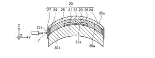
- FIG. 6 is a front view of the semi-finished lens 20.
- 7 is a cross-sectional view taken along line BB in FIG.
- the semi-finished lens 20 is processed into the lens 11 of the first embodiment described above by post-processing. Such a semi-finished lens 20 is also an object of the present invention.
- the semi-finished lens 20 includes a first intermediate substrate 21, a first adhesive layer 22, a film element 23, a spacer member 24, a second intermediate substrate 25, a second intermediate adhesive layer 26, and a fixing member 27.
- the first intermediate substrate 21 (also referred to as a first substrate) will be described with reference to FIG.
- the first intermediate substrate 21 is an optical element made of a transparent plate member having a front surface 21a and a back surface 21b.
- the first intermediate substrate 21 has a disk shape that curves convexly toward the Z direction + side.
- the surface 21a of the first intermediate substrate 21 is a convex curved surface that curves in a convex shape toward the Z direction + side.
- the back surface 21b of the first intermediate substrate 21 is a concave curved surface that is concavely curved toward the Z direction + side.
- the surface 21a is finished to an optical surface by finishing.
- the back surface 21b is an unfinished surface that has not been finished. Such a back surface 21b is finished into an optical surface by post-processing.
- the surface 21a is a spherical surface having a single curvature.
- the back surface 21b is also a spherical surface having a single curvature.
- the back surface 21b is processed into a shape according to the user's visual acuity, for example, by post-processing.
- At least one surface of the front surface 21a and the back surface 21b may be a complex curved surface having a plurality of curvatures. Further, at least one of the front surface 21a and the back surface 21b may be a flat surface.
- the material of the first intermediate substrate 21 is the same as the material of the first substrate 111 of the first embodiment described above.
- the first adhesive layer 22 will be described with reference to FIG.
- the first adhesive layer 22 is disposed between the front surface 21 a of the first intermediate substrate 21 and the back surface of the film element 23, and fixes the film element 23 and the first intermediate substrate 21.
- Such a first adhesive layer 22 is a sheet-like member whose outer shape is substantially the same as that of a film element 23 described later. In a state of being fixed to the first intermediate substrate 21, the first adhesive layer 22 is curved in a convex shape toward the Z direction + side.
- the first adhesive layer 22 is made of, for example, a film-like adhesive made of an optical pressure-sensitive adhesive, a thermosetting adhesive, or an ultraviolet curable adhesive.
- the structure of the film element 23 will be described with reference to FIG.
- the film element 23 (also referred to as an electric element) is a film-like optical element whose optical characteristics are changed by electrical control.
- Such a film element 23 is fixed to the surface 21 a of the first intermediate substrate 21 via the first adhesive layer 22.
- the film element 23 In a state of being fixed to the first intermediate substrate 21, the film element 23 is curved in a convex shape toward the Z direction + side along the surface 21 a of the first intermediate substrate 21.
- the film element 23 is a laminate in which an inner first electrode, a liquid crystal layer, and an inner second electrode are arranged in order from the first film side between the first film member and the second film member. Structure.
- the inner first electrode and the inner second electrode correspond to the first electrode 112 and the second electrode 114 of the first embodiment described above.
- the liquid crystal layer corresponds to the liquid crystal layer 113 of the first embodiment.
- the peripheral edges of the first film member and the second film member are fixed by an adhesive layer.
- the adhesive layer fixes the first film member and the second film member, and also has a function of sealing the liquid crystal material constituting the liquid crystal layer.
- the spacer member 24 will be described with reference to FIG.
- the spacer member 24 is provided between the first intermediate substrate 21 and the second intermediate substrate 25 so that the first intermediate substrate 21 and the second intermediate substrate 25 are closer than the thickness dimension of the spacer member 24. To prevent.
- Such spacer members 24 are arranged at a plurality of locations (three locations in the present embodiment) on the outer peripheral edge of the surface 21a of the first intermediate substrate 21.
- the spacer members 24 are preferably arranged at equal intervals (for example, at intervals of 120 degrees) in the direction along the outer peripheral edge of the first intermediate substrate 21.
- the spacer member 24 is a columnar member and has a predetermined thickness dimension.
- One end portion (end portion on the Z direction + side) of the spacer member 24 is fixed to the back surface 25b of the second intermediate substrate 25 with, for example, an adhesive.
- the other end portion (the end portion on the Z direction side) of the spacer member 24 is fixed to the surface 21a of the first intermediate substrate 21 with, for example, an adhesive.
- the second intermediate adhesive layer 26 is disposed between the first intermediate substrate 21 and the second intermediate substrate 25.
- a space 201 is formed.
- the thickness dimension of the space 201 is equal to the thickness dimension of the spacer member 24. Further, the thickness dimension of the space 201 is larger than the thickness dimension of the film element 23.
- the spacer member 24 as described above is removed in post-processing (specifically, peripheral processing).
- the spacer member may be a partial cylindrical shape having a discontinuous portion at one place in the circumferential direction.
- the discontinuous part is a supply port for supplying a curable composition constituting the second intermediate adhesive layer 26 described later to the space 201.
- the spacer member may be a cylindrical shape that is continuous over the entire circumference.
- Such a cylindrical spacer member has a through-hole or notch penetrating from the inner peripheral surface to the outer peripheral surface in at least one place in the circumferential direction.
- the through hole and the notch are supply ports for supplying the space 201 with the curable composition constituting the second intermediate adhesive layer 26.
- the second intermediate substrate 25 (also referred to as a second substrate) will be described with reference to FIG.
- the second intermediate substrate 25 is disposed on the Z direction + side from the film element 23 and covers the film element 23 via the second intermediate adhesive layer 26.
- Such a second intermediate substrate 25 is an optical element made of a transparent plate member. Specifically, the second intermediate substrate 25 has a disk shape that curves convexly toward the Z direction + side.
- the surface 25a of the second intermediate substrate 25 is a convex curved surface that curves in a convex shape toward the Z direction + side.
- the back surface 25b of the second intermediate substrate 25 is a concave curved surface that is concavely curved toward the Z direction + side.
- the front surface 25a and the back surface 25b are finished to optical surfaces by finishing.
- the surface 25a is a spherical surface having a single curvature.
- the back surface 25b is also a spherical surface having a single curvature.
- the curvature of the front surface 25a and the curvature of the back surface 25b are in a relationship such that the distance between the front surface 25a and the back surface 25b is constant throughout.
- At least one of the front surface 25a and the back surface 25b may be a complex curved surface having a plurality of curvatures. Further, at least one of the front surface 25a and the back surface 25b may be a flat surface.
- the material of the second intermediate substrate 25 is the same as the material of the second substrate 115 of the first embodiment described above. That is, also in this embodiment, the second intermediate substrate 25 is different from the first intermediate substrate 21 in the transmittance for light in a predetermined wavelength range.
- the second intermediate adhesive layer 26 will be described with reference to FIG.
- the second intermediate adhesive layer 26 is disposed in the space 201 between the first intermediate substrate 21 and the second intermediate substrate 25, and fixes the first intermediate substrate 21 and the second intermediate substrate 25, and the film element 23. Protect from impact.
- the second intermediate adhesive layer 26 is an optical element made of a transparent plate member. Specifically, the second intermediate adhesive layer 26 has a disk shape that curves convexly toward the Z direction + side.
- the surface of the second intermediate adhesive layer 26 is a convex curved surface that curves in a convex shape toward the Z direction + side.
- the back surface of the second intermediate adhesive layer 26 is a concave curved surface that is concavely curved toward the Z direction + side.
- the second intermediate adhesive layer 26 has a recess 26a for disposing the film element 23 on the back surface.
- the second intermediate adhesive layer 26 as described above is formed by injecting a curable composition into the space 201 via a communicating portion 27a of the fixing member 27 described later and curing it.
- the curable composition constituting the second intermediate adhesive layer 26 include various optical adhesives.
- a photocurable adhesive that is photocured by irradiation with light energy rays such as ultraviolet rays or visible rays is preferable.
- the thermosetting type adhesive agent which thermosets by applying a thermal energy is also mentioned.
- Each of these adhesives preferably has a low viscosity.
- the fixing member 27 has, for example, a tape shape and is wound around the outer peripheral surface of the first intermediate substrate 21 and the outer peripheral surface of the second intermediate substrate 25 so as to surround the space 201.
- the fixing member 27 also has a function of fixing the first intermediate substrate 21 and the second intermediate substrate 25.
- Such a fixing member 27 has a communication portion 27a that communicates the space 201 with the external space in at least one place in the circumferential direction.
- step S201 of FIG. 10 the operator attaches the surface of the film-like first adhesive layer 22 to the back surface of the film element 23, thereby making the first assembly M1 (see FIG. 8A).
- the film element 23 and the first adhesive layer 22 are not curved.
- step S202 of FIG. 10 the operator attaches the back surface of the first adhesive layer 22 in the first assembly M1 to the front surface 21a of the first intermediate substrate 21, and then the second assembly M2 (see FIG. 8B). ).
- the first intermediate substrate 21 is manufactured by a known method such as injection molding.
- the outer shape of the first intermediate substrate 21 in plan view is a shape that includes the outer shape of the lens 11 in plan view. That is, the outer shape of the first intermediate substrate 21 in plan view is larger than the outer shape of the lens 11 in plan view.
- the first intermediate substrate 21 is a common component common to the semi-finished lens 20 having the same size. Therefore, the first intermediate substrate 21 is manufactured by a common manufacturing method.
- the operation of attaching the first assembly M1 to the surface 21a of the first intermediate substrate 21 is performed using a jig (not shown).
- the jig has a holding surface capable of holding the first assembly M1.
- the holding surface is pressed against the surface 21a, the holding surface is elastically deformed along the surface 21a.
- the film element 23 is attached to the surface 21a while being deformed along the surface 21a.
- step S203 of FIG. 10 the operator arranges the plurality of spacer members 24 around the portion of the surface 21a of the first intermediate substrate 21 where the film element 23 is fixed, and the third assembly M3 ( 8C).
- the third assembly M3 the other end portions (end portions on the Z direction side) of the spacer members 24 are respectively fixed to the surface 21a of the first intermediate substrate 21 with an adhesive, for example.
- step S204 of FIG. 10 the worker arranges the second intermediate substrate 25 on the Z direction + side of the first intermediate substrate 21 to make the fourth assembly M4 (see FIG. 8D).
- the fourth assembly M4 one end portion (end portion on the Z direction + side) of each spacer member 24 is fixed to the back surface 25b of the second intermediate substrate 25 by, for example, an adhesive.
- a space 201 exists between the first intermediate substrate 21 and the second intermediate substrate 25.
- Such a second intermediate substrate 25 is manufactured by a known method such as injection molding.
- the second intermediate substrate 25 is a non-common component that can be selected according to desired optical characteristics in the same size semi-finished lens 20 of the same size. That is, with respect to the second intermediate substrate 25, a plurality of types of second intermediate substrates 25 that are different from the first intermediate substrate 21 in transmittance for light in a predetermined wavelength range are manufactured. The operator selects the second intermediate substrate 25 according to the desired optical characteristics from among them.
- the additive When the additive is added by coating or dyeing, the intermediate lens produced by injection molding is coated or dyed. Moreover, when the addition method of an additive is kneading, an additive is added with respect to the molten base material used by injection molding before injection molding.
- the operator selects the second substrate 115 having desired optical characteristics from among a plurality of types of second intermediate substrates 25 having different optical characteristics, such as a photochromic lens, a blue light cut lens, and a neo-contrast lens.
- step S205 of FIG. 10 the operator winds the fixing member 27 around the outer peripheral surface of the first intermediate substrate 21 and the outer peripheral surface of the second intermediate substrate 25 so as to surround the space 201, and the fifth group A solid M5 (see FIG. 8E) is created.
- the space 201 is closed by a portion other than the communication portion 27a of the fixing member 27. In other words, the space 201 communicates with the external space only through the communication portion 27a.
- step S206 of FIG. 10 the operator can apply the curable composition constituting the second intermediate adhesive layer 26 via the communication portion 27 a of the fixing member 27. Supply to the space 201. And an operator hardens the curable composition in the space 201, and produces the semifinished lens 20 (refer FIG. 7).
- the order of the above-described steps S201 to S206 is appropriately changed within a technically consistent range. Further, the above-described steps S101 to S107 may be performed in parallel as long as there is no technical contradiction.
- the subject that performs the above-described manufacturing method is not limited to a person but may be a machine.
- Each process referring to FIGS. 8A to 8F does not include a process of applying heat.
- Such a semi-finished lens manufacturing method is effective in preventing deformation or damage of the first intermediate substrate 21, the second intermediate substrate 25, and the film element 23.
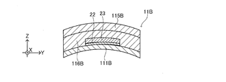
- the semi-finished lens 20 is processed into the lens 11B (see FIG. 9) by post-processing the semi-finished lens 20 obtained by the above manufacturing method. Although a detailed description of the post-processing is omitted, the semi-finished lens 20 is processed into the lens 11 by removing the removal portion 202 (portion surrounded by a two-dot chain line in FIG. 7) by post-processing.
- the semi-finished lens 20 is processed into the lens 11B (see FIG. 9) by post-processing the semi-finished lens 20 obtained by the above manufacturing method. Although a detailed description of the post-processing is omitted, the semi-finished lens 20 is processed into the lens 11 by removing the removal portion 202 (portion surrounded by a two-dot chain line in FIG. 7) by post-processing.
- the first intermediate substrate 21 of the semi-finished lens 20 becomes the first substrate 111B of the lens 11B after being subjected to post-processing.
- the second intermediate substrate 25 of the semi-finished lens 20 becomes the second substrate 115B of the lens 11B after being subjected to post-processing.
- the second intermediate adhesive layer 26 of the semi-finished lens 20 becomes the adhesive layer 116B of the lens 11B.
- the spacer member 24 and the fixing member 27 of the semi-finished lens 20 are removed by post-processing.
- the post-processing includes a back surface processing for grinding the back surface of the semi-finished lens 20 by grinding and a peripheral processing for cutting the outer periphery of the semi-finished lens 20 by cutting processing and polishing processing.
- a coating process for forming a coating layer may be performed on the back surface of the semi-finished lens 20 after the back surface processing (the back surface of the second intermediate substrate 25). Moreover, you may perform the coating process which forms a coating layer in the surface (surface 21a of the 1st intermediate substrate 21) of the semifinished lens 20 at an appropriate timing.
- the coating layer includes, for example, at least one layer of a primer layer, a hard coat layer, an antireflection film layer, an antifogging coat layer, an antifouling layer, and a water repellent layer.
- the coating layer may have a multilayer structure composed of a plurality of types of layers.
- the surface side coating layer may have a single layer structure composed of one kind of layer.
- the coating process for forming such a coating layer is preferably a process in which heat is not applied to the semi-finished lens 20.
- the material of the second intermediate substrate 25 containing an additive for imparting special optical characteristics is more expensive than the material of the first intermediate substrate 21 not containing an additive.
- the volume of the second intermediate substrate 25 occupying the semi-finished lens 20 is smaller than the volume of the first intermediate substrate 21. That is, the material of the second intermediate substrate 25 used for the semifinished lens 20 is less than the material of the first intermediate substrate 21. Therefore, the configuration of the present embodiment can reduce the cost of the semi-finished lens 20 and the lens 11 as compared with the configuration in which the additive is added to the first intermediate substrate 21.
- the proportion of the second intermediate substrate 25 in the removal portion 202 (the portion surrounded by the two-dot chain line in FIG. 7) removed from the semi-finished lens 20 in the post-processing described above is larger than that of the first intermediate substrate 21. small. That is, the amount removed by post-processing is smaller in the second intermediate substrate 25 than in the first intermediate substrate 21.
- the structure of this embodiment can make the yield regarding the material containing an additive high compared with the structure which adds an additive to the material of the 1st intermediate substrate 21.
- FIG. Also from such a viewpoint, the configuration of the present embodiment is advantageous in reducing the cost of the semi-finished lens 20 and the lens 11.
- the step of adding the additive to the second intermediate substrate 25 is performed before the second intermediate substrate 25 is fixed to the first intermediate substrate 21. For this reason, in the step of adding the additive, even when heat is applied to the second intermediate substrate 25, heat is not applied to the first intermediate substrate 21 and the film element 23. Furthermore, if a photo-curing adhesive is employed as the second intermediate adhesive layer 26, heat is applied to the first intermediate substrate 21 and the film element 23 in the step of fixing the second intermediate substrate 25 and the first intermediate substrate 21. There is no participation. Such a manufacturing method is effective for preventing deformation or damage of the first intermediate substrate 21 and the film element 23.
- the film element 23 may be fixed to the second intermediate substrate 25.
- the second intermediate substrate 25 is the first substrate
- the first intermediate substrate 21 is the second substrate.
- the eyewear to which the lens according to the present invention can be applied includes glasses (including electronic glasses and sunglasses) and goggles having an auxiliary mechanism for improving the user's visual acuity like a visual acuity correction lens.
- the eyewear to which the lens according to the present invention can be applied includes various devices having a mechanism for presenting information to the user's field of view or eyes (for example, a glasses-type wearable terminal, a head-mounted display, etc.). It is.
- the eyewear to which the lens according to the present invention can be applied only needs to be able to hold an auxiliary mechanism for improving visual acuity or visibility, a mechanism for presenting information, etc. in front of or around the user's eyes.
- the eyewear to which the lens according to the present invention can be applied is not limited to the glasses type that can be worn on both ears, but may be a type that is worn on the head or one ear.
- the eyewear to which the lens according to the present invention can be applied is not limited to eyewear for both eyes, and may be eyewear for one eye.
- the lens according to the present invention is not limited to glasses lenses, but can be applied to various eyewear lenses.
Abstract
An eyewear lens according to the present invention is configured so as to be provided with: a transparent first substrate having a principal surface; a second substrate disposed facing the principal surface, the transmittance thereof with respect to light in a predetermined wavelength region being different from that of the first substrate; an electric element in which an optical characteristic thereof is changed by electrical control, the electric element being provided between the first substrate and the second substrate; and an adhesive layer provided between the first substrate and the second substrate.
Description
本発明は、アイウェア用のレンズおよびレンズの製造方法に関する。
The present invention relates to a lens for eyewear and a method for manufacturing the lens.
従来、駆動電圧の印加によって駆動する電気素子、たとえば、屈折率が変化する液晶レンズを有するレンズを備えるアイウェアが開発されている(たとえば特許文献1参照)。
2. Description of the Related Art Conventionally, eyewear including an electric element that is driven by application of a driving voltage, for example, a lens having a liquid crystal lens whose refractive index changes has been developed (for example, see Patent Document 1).
上述のようなアイウェアにおいて、用途に応じた光学特性を有するレンズが望まれている。
In the above-described eyewear, a lens having optical characteristics corresponding to the application is desired.
本発明は、このような状況に鑑みなされたものであり、用途に応じた光学特性を有するレンズを提供することを課題とする。
This invention is made in view of such a situation, and makes it a subject to provide the lens which has an optical characteristic according to a use.
本発明に係るレンズは、アイウェア用のレンズであって、主面を有し、透明な第一基板と、主面と対向して配置され、所定の波長域の光に対する透過率が第一基板と異なる第二基板と、第一基板と第二基板との間に設けられ、電気的制御により光学特性が変化する電気素子と、第一基板と第二基板との間に設けられた接着層とを備える。
A lens according to the present invention is a lens for eyewear, has a main surface, is disposed opposite to the main surface with a transparent first substrate, and has a first transmittance with respect to light in a predetermined wavelength region. A second substrate different from the substrate, an electrical element that is provided between the first substrate and the second substrate, and whose optical characteristics are changed by electrical control, and an adhesive provided between the first substrate and the second substrate And a layer.
本発明に係るレンズの製造方法は、アイウェア用のレンズの製造方法であって、電気的制御により光学特性が変化する電気素子を第一基板に設けるステップと、所定の波長域の光に対する透過率が前記第一基板と異なる第二基板を、第一基板に固定するステップと、を含む。
The method for manufacturing a lens according to the present invention is a method for manufacturing a lens for eyewear, the step of providing an electrical element whose optical characteristics are changed by electrical control on a first substrate, and transmission of light in a predetermined wavelength range. Fixing a second substrate having a rate different from that of the first substrate to the first substrate.
本発明によれば、用途に応じた光学特性を有するレンズを提供することを課題とする。
According to the present invention, it is an object to provide a lens having optical characteristics according to the application.
以下、本発明の実施形態について、図面を用いて詳細に説明する。以下の説明では、本発明に係るアイウェア用のレンズの代表例として、電気的制御によって、その光学特性を変化させることができる電気素子を有する視力矯正用のレンズについて説明する。
Hereinafter, embodiments of the present invention will be described in detail with reference to the drawings. In the following description, as a representative example of the eyewear lens according to the present invention, a vision correction lens having an electrical element whose optical characteristics can be changed by electrical control will be described.
[実施形態1]
図1~図4を参照して、本発明の実施形態1に係る電子メガネ100について説明する。 [Embodiment 1]
Theelectronic glasses 100 according to Embodiment 1 of the present invention will be described with reference to FIGS.
図1~図4を参照して、本発明の実施形態1に係る電子メガネ100について説明する。 [Embodiment 1]
The
<電子メガネについて>
図1は、本実施形態に係る電子メガネ100の構成の一例を示す斜視図である。図2は、電子メガネ100の内部回路を示すブロック図である。電子メガネ100は、フレーム10、一対のレンズ11、制御部13、検出部14、および一対の電源15を有する。 <About electronic glasses>
FIG. 1 is a perspective view illustrating an example of the configuration of theelectronic glasses 100 according to the present embodiment. FIG. 2 is a block diagram showing an internal circuit of the electronic glasses 100. The electronic glasses 100 includes a frame 10, a pair of lenses 11, a control unit 13, a detection unit 14, and a pair of power supplies 15.
図1は、本実施形態に係る電子メガネ100の構成の一例を示す斜視図である。図2は、電子メガネ100の内部回路を示すブロック図である。電子メガネ100は、フレーム10、一対のレンズ11、制御部13、検出部14、および一対の電源15を有する。 <About electronic glasses>
FIG. 1 is a perspective view illustrating an example of the configuration of the
<フレームについて>
フレーム10は、フロント101および一対のテンプル102を有する。なお、以下、フロント101が配置される部分を電子メガネ100の正面(前方)とする。一対のテンプル102は、制御部13、検出部14、および一対の電源15を保持する。なお、一対の電源15は、何れか一方のみでもよい。この場合には、電源15は、一対のテンプル102のうちの一方のテンプル102(たとえば、右用のテンプル102)にのみ保持される。 <About the frame>
Theframe 10 has a front 101 and a pair of temples 102. Hereinafter, the portion where the front 101 is arranged is referred to as the front (front) of the electronic glasses 100. The pair of temples 102 holds the control unit 13, the detection unit 14, and the pair of power sources 15. Note that only one of the pair of power supplies 15 may be used. In this case, the power supply 15 is held only in one of the pair of temples 102 (for example, the right temple 102).
フレーム10は、フロント101および一対のテンプル102を有する。なお、以下、フロント101が配置される部分を電子メガネ100の正面(前方)とする。一対のテンプル102は、制御部13、検出部14、および一対の電源15を保持する。なお、一対の電源15は、何れか一方のみでもよい。この場合には、電源15は、一対のテンプル102のうちの一方のテンプル102(たとえば、右用のテンプル102)にのみ保持される。 <About the frame>
The
電子メガネ100のユーザ(装着者)は、テンプル102に設けられた検出部14を操作(たとえば、タッチ操作)することにより、レンズ11の液晶レンズ部11aの光学特性(たとえば、透過率)を切り替える。
A user (wearer) of the electronic glasses 100 switches the optical characteristic (for example, transmittance) of the liquid crystal lens unit 11 a of the lens 11 by operating (for example, touching) the detection unit 14 provided on the temple 102. .
ユーザにより検出部14が操作されると、制御部13は、当該操作に基づいて、液晶レンズ部11aに電圧を印可した状態と、電圧を印可しない状態とを切り替える。
When the detection unit 14 is operated by the user, the control unit 13 switches between a state where a voltage is applied to the liquid crystal lens unit 11a and a state where no voltage is applied based on the operation.
<レンズについて>
図3は、図1のA-A線断面図である。図4には、電子メガネ100を前方から見たときに、左側に配置されるレンズ11が示される。 <About the lens>
3 is a cross-sectional view taken along line AA in FIG. FIG. 4 shows thelens 11 arranged on the left side when the electronic glasses 100 are viewed from the front.
図3は、図1のA-A線断面図である。図4には、電子メガネ100を前方から見たときに、左側に配置されるレンズ11が示される。 <About the lens>
3 is a cross-sectional view taken along line AA in FIG. FIG. 4 shows the
以下、レンズ11の構成を説明するにあたり、説明の便宜のために、直交座標系(X,Y,Z)を使用する。各図に示される直交座標系(X,Y,Z)は、共通の直交座標系である。
Hereinafter, in describing the configuration of the lens 11, an orthogonal coordinate system (X, Y, Z) is used for convenience of explanation. The orthogonal coordinate system (X, Y, Z) shown in each figure is a common orthogonal coordinate system.
X方向は、アイウェアをユーザが装着した状態(以下、単に「装着状態」という。)において、ユーザの左右方向に一致する。Y方向は、装着状態において、ユーザの上下方向に一致する。Z方向は、装着状態において、ユーザの前後方向およびレンズ11の光軸の方向に一致する。
The X direction coincides with the left and right direction of the user when the eyewear is worn by the user (hereinafter simply referred to as “wearing state”). The Y direction coincides with the vertical direction of the user in the mounted state. The Z direction coincides with the front-rear direction of the user and the direction of the optical axis of the lens 11 in the mounted state.
また、以下の説明において、特に断ることなく「厚さ方向」といった場合には、レンズ11の厚さ方向を意味する。厚さ方向は、上述の直交座標系のZ方向に一致する。
In the following description, the term “thickness direction” means the thickness direction of the lens 11 without particular notice. The thickness direction coincides with the Z direction of the orthogonal coordinate system described above.
また、各部材の「表面」は、装着状態において、ユーザから遠い側(Z方向+側)の面である。一方、各部材の「裏面」は、装着状態において、ユーザに近い側(Z方向-側)の面である。
Also, the “surface” of each member is a surface on the side far from the user (Z direction + side) in the mounted state. On the other hand, the “back surface” of each member is a surface closer to the user (Z direction-side) in the mounted state.
本実施形態の場合、レンズ11は、Z方向+側に向かって凸状に湾曲する。ただし、図3において、レンズ11の曲率は、ゼロとして示される。
In the case of this embodiment, the lens 11 is curved in a convex shape toward the Z direction + side. However, in FIG. 3, the curvature of the lens 11 is shown as zero.
一対のレンズ11は、電子メガネ100を正面視したときに、左右対称となるように形成されており、互いに同一の構成要素を有する。そこで、以下の説明では、電子メガネ100の右目用のレンズ11について説明し、左目用のレンズ11については、その説明を省略する。
The pair of lenses 11 are formed so as to be symmetric when the electronic glasses 100 are viewed from the front, and have the same components. Therefore, in the following description, the lens 11 for the right eye of the electronic glasses 100 will be described, and the description of the lens 11 for the left eye will be omitted.
レンズ11は、液晶レンズ部11a、および、液晶レンズ部11a以外の部分である通常レンズ部11bを有する。
The lens 11 has a liquid crystal lens part 11a and a normal lens part 11b which is a part other than the liquid crystal lens part 11a.
液晶レンズ部11aは、電圧によりその焦点距離(度数)を切替え可能である。図3に示されるように、液晶レンズ部11aは、後方側(Z方向-側)から順に、第一基板111、第一電極112、液晶層113、第二電極114、および第二基板115を有する。なお、第一電極112、液晶層113および第二電極114は、電気素子を構成する。
The liquid crystal lens unit 11a can switch its focal length (frequency) by voltage. As shown in FIG. 3, the liquid crystal lens unit 11a includes a first substrate 111, a first electrode 112, a liquid crystal layer 113, a second electrode 114, and a second substrate 115 in order from the rear side (Z direction-side). Have. The first electrode 112, the liquid crystal layer 113, and the second electrode 114 constitute an electric element.
通常レンズ部11bは、後方側から順に、第一基板111、第一電極112、接着層116、第二電極114、および第二基板115を有する。液晶レンズ部11aと通常レンズ部11bとは、第一基板111、第一電極112、第二電極114、および第二基板115を共有する。液晶レンズ部11aおよび通常レンズ部11bの構成要素はそれぞれ、可視光に対して透光性を有する。
The normal lens portion 11b includes a first substrate 111, a first electrode 112, an adhesive layer 116, a second electrode 114, and a second substrate 115 in order from the rear side. The liquid crystal lens unit 11a and the normal lens unit 11b share the first substrate 111, the first electrode 112, the second electrode 114, and the second substrate 115. The components of the liquid crystal lens unit 11a and the normal lens unit 11b are each translucent to visible light.
<第一基板について>
第一基板111は、Z方向+側(図3の上側)に向かって凸状に湾曲する板状である。第一基板111の表面111aは、Z方向+側に向かって凸状に湾曲する凸曲面である。また、第一基板111の裏面111bは、Z方向+側に向かって凹状に湾曲する凹曲面である。 <About the first substrate>
Thefirst substrate 111 has a plate shape that curves in a convex shape toward the Z direction + side (upper side in FIG. 3). The surface 111a of the first substrate 111 is a convex curved surface that curves in a convex shape toward the Z direction + side. The back surface 111b of the first substrate 111 is a concave curved surface that curves in a concave shape toward the Z direction + side.
第一基板111は、Z方向+側(図3の上側)に向かって凸状に湾曲する板状である。第一基板111の表面111aは、Z方向+側に向かって凸状に湾曲する凸曲面である。また、第一基板111の裏面111bは、Z方向+側に向かって凹状に湾曲する凹曲面である。 <About the first substrate>
The
第一基板111は、場所によって、レンズ11の光軸の方向における厚さ寸法が異なる。たとえば、近視矯正用のレンズ(マイナスレンズともいう。)の場合には、第一基板111は、外周縁における厚さ寸法が、最も大きい。また、遠視矯正用のレンズ(プラスレンズともいう。)の場合には、第一基板111は、外周縁における厚さ寸法が、最も小さい。なお、第一基板111は、全体にわたり、レンズ11の光軸の方向における厚さ寸法が等しくてもよい。
The thickness dimension of the first substrate 111 in the direction of the optical axis of the lens 11 varies depending on the location. For example, in the case of a lens for correcting myopia (also referred to as a minus lens), the first substrate 111 has the largest thickness dimension at the outer periphery. In the case of a lens for hyperopia correction (also referred to as a plus lens), the first substrate 111 has the smallest thickness dimension at the outer periphery. The first substrate 111 may have the same thickness dimension in the direction of the optical axis of the lens 11 throughout.
なお、表面111aおよび裏面111bはそれぞれ、単一の曲率を有する球面であってもよいし、複数の曲率を有する複合曲面であってもよい。また、表面111aおよび裏面111bの少なくとも一方の面は、平面であってもよい。
Note that each of the front surface 111a and the back surface 111b may be a spherical surface having a single curvature or a complex curved surface having a plurality of curvatures. Further, at least one of the front surface 111a and the back surface 111b may be a flat surface.
第一基板111は、表面111aの液晶レンズ部11aに対応する部分に、回折領域111cを有する。回折領域111cは、中央部分に配置される半球状の凸部111dと、凸部111dを中心とした同心円上に配置される複数の円環状の第一凸条111eとを有する。
The first substrate 111 has a diffraction region 111c in a portion corresponding to the liquid crystal lens portion 11a of the surface 111a. The diffractive region 111c includes a hemispherical convex portion 111d disposed in the central portion, and a plurality of annular first convex strips 111e disposed on a concentric circle with the convex portion 111d as the center.
凸部111dおよび第一凸条111eの形状の例として、フレネルレンズ形状が挙げられる。なお、凸部111dおよび第一凸条111eは、一部がフレネルレンズ形状であってもよいし、全部がフレネルレンズ形状であってもよい。
Examples of the shape of the convex portion 111d and the first convex strip 111e include a Fresnel lens shape. In addition, a part of convex part 111d and the 1st convex strip 111e may be a Fresnel lens shape, and all may be a Fresnel lens shape.
第一基板111は、無機ガラスまたは有機ガラスから造られる。第一基板111は、有機ガラスから造られるのが好ましい。有機ガラスは、熱硬化性ポリウレタン類、ポリチオウレタン類、ポリエポキシド類、もしくはポリエピスルフィド類からなる熱硬化性材料、もしくはポリ(メタ)アクリレート類からなる熱可塑性材料、または、これらの共重合体もしくは混合物からなる熱硬化性(架橋した)材料の何れかである。ただし、第一基板111の材料は、これらに限定されず、レンズの材料として使用される公知の材料が採用されうる。また、レンズの厚み軽減などの観点から、第一基板111および第二基板115の屈折率は高いことが好ましい。第一基板111および第二基板115の屈折率は、1.55以上であることが好ましく、1.65以上であることがより好ましい。
The first substrate 111 is made of inorganic glass or organic glass. The first substrate 111 is preferably made of organic glass. The organic glass is a thermosetting material made of thermosetting polyurethanes, polythiourethanes, polyepoxides, or polyepisulfides, or a thermoplastic material made of poly (meth) acrylates, or a copolymer thereof or Any of thermosetting (cross-linked) materials consisting of a mixture. However, the material of the 1st board | substrate 111 is not limited to these, The well-known material used as a material of a lens can be employ | adopted. Further, from the viewpoint of reducing the thickness of the lens, it is preferable that the refractive index of the first substrate 111 and the second substrate 115 is high. The refractive indexes of the first substrate 111 and the second substrate 115 are preferably 1.55 or more, and more preferably 1.65 or more.
<第一電極および第二電極について>
第一電極112および第二電極114は、透光性を有する一対の透明電極である。第一電極112は、第一基板111と液晶層113との間に配置される。第二電極114は、液晶層113と第二基板115との間に配置される。 <About the first electrode and the second electrode>
Thefirst electrode 112 and the second electrode 114 are a pair of transparent electrodes having translucency. The first electrode 112 is disposed between the first substrate 111 and the liquid crystal layer 113. The second electrode 114 is disposed between the liquid crystal layer 113 and the second substrate 115.
第一電極112および第二電極114は、透光性を有する一対の透明電極である。第一電極112は、第一基板111と液晶層113との間に配置される。第二電極114は、液晶層113と第二基板115との間に配置される。 <About the first electrode and the second electrode>
The
第一電極112および第二電極114は、少なくとも液晶層113に電圧を印加できる範囲(液晶レンズ部11a)に亘って配置されていればよい。
The first electrode 112 and the second electrode 114 may be disposed over at least a range (liquid crystal lens portion 11a) in which a voltage can be applied to the liquid crystal layer 113.
第一電極112および第二電極114の材料は、所期の透光性および導電性を有していれば特に限定されない。第一電極112および第二電極114の例として、酸化インジウムスズ(ITO)および酸化亜鉛(ZnO)などが挙げられる。第一電極112および第二電極114の材料は、互いに同じで、または異なっていてもよい。
The material of the first electrode 112 and the second electrode 114 is not particularly limited as long as the material has the desired translucency and conductivity. Examples of the first electrode 112 and the second electrode 114 include indium tin oxide (ITO) and zinc oxide (ZnO). The materials of the first electrode 112 and the second electrode 114 may be the same as or different from each other.
<液晶層について>
液晶層113は、第一電極112と第二電極114との間に配置される。液晶層113は、電圧の印加の有無に応じて、その屈折率が変化するように構成される。たとえば、液晶層113の屈折率は、液晶層113に電圧が印加されていない状態において、第一基板111の屈折率および第二基板115の屈折率とほぼ同じであるように調整される。一方、液晶層113の屈折率は、液晶層113に電圧が印加されている状態において、第一基板111の屈折率および第二基板115の屈折率と異なるように調整される。 <About the liquid crystal layer>
Theliquid crystal layer 113 is disposed between the first electrode 112 and the second electrode 114. The liquid crystal layer 113 is configured such that its refractive index changes depending on whether or not a voltage is applied. For example, the refractive index of the liquid crystal layer 113 is adjusted to be substantially the same as the refractive index of the first substrate 111 and the refractive index of the second substrate 115 in a state where no voltage is applied to the liquid crystal layer 113. On the other hand, the refractive index of the liquid crystal layer 113 is adjusted to be different from the refractive index of the first substrate 111 and the refractive index of the second substrate 115 when a voltage is applied to the liquid crystal layer 113.
液晶層113は、第一電極112と第二電極114との間に配置される。液晶層113は、電圧の印加の有無に応じて、その屈折率が変化するように構成される。たとえば、液晶層113の屈折率は、液晶層113に電圧が印加されていない状態において、第一基板111の屈折率および第二基板115の屈折率とほぼ同じであるように調整される。一方、液晶層113の屈折率は、液晶層113に電圧が印加されている状態において、第一基板111の屈折率および第二基板115の屈折率と異なるように調整される。 <About the liquid crystal layer>
The
液晶層113は、液晶材料を含有する。電圧が印加されているときの当該液晶材料の配向状態と、電圧が印加されていないときの当該液晶材料の配向状態とは、互いに異なる。液晶材料は、第一基板111の屈折率および第二基板115の屈折率に応じて、適宜選択されうる。たとえば、液晶材料は、コレステリック液晶やネマチック液晶などにより構成されうる。
The liquid crystal layer 113 contains a liquid crystal material. The alignment state of the liquid crystal material when a voltage is applied is different from the alignment state of the liquid crystal material when a voltage is not applied. The liquid crystal material can be appropriately selected according to the refractive index of the first substrate 111 and the refractive index of the second substrate 115. For example, the liquid crystal material can be composed of cholesteric liquid crystal, nematic liquid crystal, or the like.
<第二基板について>
第二基板115は、第一基板111よりも前方に、第一基板111の表面111aに対向する状態で配置される。第二基板115は、前方側に向かって凸状に湾曲する板状である。第二基板115の表面115aは、Z方向+側に向かって凸状に湾曲する凸曲面である。第一基板111の裏面115bは、Z方向+側に向かって凹状に湾曲する凹曲面である。 <About the second substrate>
Thesecond substrate 115 is disposed in front of the first substrate 111 so as to face the surface 111 a of the first substrate 111. The second substrate 115 has a plate shape that curves convexly toward the front side. The surface 115a of the second substrate 115 is a convex curved surface that curves in a convex shape toward the Z direction + side. The back surface 115b of the first substrate 111 is a concave curved surface that curves concavely toward the Z direction + side.
第二基板115は、第一基板111よりも前方に、第一基板111の表面111aに対向する状態で配置される。第二基板115は、前方側に向かって凸状に湾曲する板状である。第二基板115の表面115aは、Z方向+側に向かって凸状に湾曲する凸曲面である。第一基板111の裏面115bは、Z方向+側に向かって凹状に湾曲する凹曲面である。 <About the second substrate>
The
第二基板115は、全体にわたり、レンズ11の光軸の方向における厚さ寸法が等しい。本実施形態において、第二基板115の上記光軸の方向における厚さ寸法が等しいとは、±10%の誤差(±0.1W)を含んでよい。なお、第二基板115は、場所によって、レンズ11の光軸の方向における厚さ寸法が異なってもよい。また、表面115aおよび裏面115bはそれぞれ、単一の曲率を有する球面であってもよいし、複数の曲率を有する複合曲面であってもよい。また、表面115aおよび裏面115bの少なくとも一方の面は、平面であってもよい。
The second substrate 115 has the same thickness dimension in the direction of the optical axis of the lens 11 throughout. In the present embodiment, that the thickness dimension in the direction of the optical axis of the second substrate 115 is equal may include an error (± 0.1 W) of ± 10%. The second substrate 115 may have a different thickness dimension in the direction of the optical axis of the lens 11 depending on the location. Further, each of the front surface 115a and the back surface 115b may be a spherical surface having a single curvature or a complex curved surface having a plurality of curvatures. Further, at least one of the front surface 115a and the back surface 115b may be a flat surface.
第二基板115は、所定の波長域の光に対する透過率が第一基板111と異なる。このために、第二基板115は、第一基板111が有していない添加剤を含む。なお、第二基板115の基材は、第一基板111と同じである。また、第二基板115の屈折率(第二屈折率)と、第一基板111の屈折率(第一屈折率)とは等しい。本実施形態において、第一屈折率と第二屈折率とが等しいとは、第一屈折率と第二屈折率との差が±0.1の範囲を含んでよい。
The second substrate 115 is different from the first substrate 111 in transmittance for light in a predetermined wavelength range. Therefore, the second substrate 115 includes an additive that the first substrate 111 does not have. The base material of the second substrate 115 is the same as that of the first substrate 111. The refractive index (second refractive index) of the second substrate 115 is equal to the refractive index (first refractive index) of the first substrate 111. In the present embodiment, that the first refractive index and the second refractive index are equal may include a range where the difference between the first refractive index and the second refractive index is ± 0.1.
添加剤として、フォトクロミック化合物、紫外線を選択的に吸収する選択吸収剤(以下、「紫外線吸収剤」という。)、高エネルギー可視光線(400~500nmのうち、特に400~420nmの短波調光)である青色光を選択的に吸収する選択吸収剤(以下、「青色選択吸収剤」という。)、希土類金属化合物(たとえばネオジム化合物)、および有機系色素(たとえばポルフィリン化合物)などが挙げられる。
As an additive, a photochromic compound, a selective absorber that selectively absorbs ultraviolet rays (hereinafter referred to as “ultraviolet absorber”), high energy visible light (short wavelength dimming of 400 to 500 nm, particularly 400 to 420 nm). Examples thereof include a selective absorber that selectively absorbs blue light (hereinafter referred to as “blue selective absorber”), a rare earth metal compound (for example, a neodymium compound), and an organic dye (for example, a porphyrin compound).
フォトクロミック化合物が添加されたレンズは、屋内では透明色のレンズとして機能し、屋外では太陽光(紫外線)に反応してレンズがグレー、ブラウンなどに発色し、眩しさから目を守る機能を発揮する。フォトクロミック化合物を添加されたレンズが発色していない状態を、第二基板の通常状態と称することもある。フォトクロミック化合物を添加されたレンズが発色した状態を、第二基板の発色状態と称することもある。このようなレンズを有する眼鏡は、屋内および屋外の両方での使用に対応する高機能な眼鏡であり、近年、その需要が拡大している。
Lenses with added photochromic compounds function as transparent lenses indoors, and in the outdoors they respond to sunlight (ultraviolet rays), causing the lenses to turn gray, brown, etc., and protect the eyes from glare. . The state where the lens to which the photochromic compound is added is not colored is sometimes referred to as the normal state of the second substrate. The state in which the lens to which the photochromic compound is added is colored is sometimes referred to as the colored state of the second substrate. The spectacles having such a lens are highly functional spectacles that can be used both indoors and outdoors, and in recent years, the demand thereof has been increasing.
フォトクロミック化合物として、種々のものを用いることができる。例えば、フォトクロミック化合物として、国際公開第2012/141306号パンフレット、特開2004-78052号公報、国際公開第2014/208994号パンフレット、特開平8-272036号公報、特開2005-23238号公報、および、特開2008-30439号公報に記載のフォトクロミック化合物が挙げられる。
Various kinds of photochromic compounds can be used. For example, as photochromic compounds, International Publication No. 2012/141306, Japanese Patent Application Laid-Open No. 2004-78052, International Publication No. 2014/208994, Japanese Patent Application Laid-Open No. 8-27236, Japanese Patent Application Laid-Open No. 2005-23238, and And photochromic compounds described in JP-A-2008-30439.
具体的には、フォトクロミック化合物として、スピロピラン系化合物、クロメン系化合物、スピロオキサジン系化合物、フルギド系化合物、および、ビスイミダゾール系化合物の中から所望の着色に応じて、1種または2種以上を混合したフォトクロミック化合物が挙げられる。
Specifically, as a photochromic compound, one or more of spiropyran compounds, chromene compounds, spirooxazine compounds, fulgide compounds, and bisimidazole compounds are mixed depending on the desired coloration. Photochromic compounds.
また、フォトクロミック化合物は、公知の方法で合成することができる。たとえば、特表2004-500319号、国際公開第2009/146509号パンフレット、国際公開第2010/20770号パンフレット、国際公開第2012/149599号パンフレット、および、国際公開第2012/162725号パンフレットに記載の方法により得られる。
The photochromic compound can be synthesized by a known method. For example, the methods described in JP-T-2004-500319, International Publication No. 2009/146509, International Publication No. 2010/20770, International Publication No. 2012/149599, and International Publication No. 2012/162725 Is obtained.
紫外線吸収剤が添加されたレンズは、紫外線による障害から目などを保護することができる。近年、波長400nm以下の紫外線は、角膜や水晶体に悪影響を及ぼすことが知られており、このような紫外線を効果的に吸収できるレンズが求められている。
A lens to which an ultraviolet absorber is added can protect the eyes from damage caused by ultraviolet rays. In recent years, ultraviolet rays having a wavelength of 400 nm or less are known to have an adverse effect on the cornea and the crystalline lens, and a lens capable of effectively absorbing such ultraviolet rays is required.
たとえば、第一基板111および第二基板115にポリウレタン系樹脂原料であるイソ(チオ)シアナート、ポリチオールを用いる場合、2-[2-ヒドロキシ-3-(ジメチルベンジル)-5-(1,1,3,3-テトラメチルブチル)フェニル]-2H-ベンゾトリアゾール、イソオクチル-3-(3-(2H-ベンゾトリアゾール-2-イル)-5-t-ブチル-4-ヒドロキシフェニルプロピオネート、2-[2-ヒドロキシ-3,5-ビス(ジメチルベンジル)フェニル]-2H-ベンゾトリアゾールといったベンゾトリアゾール系紫外線吸収剤を添加し、ポリウレタン系樹脂を製造する。このようなポリウレタン系樹脂は、光学物性低下のない無色透明で高い紫外線カット率を有する。このようなポリウレタン系樹脂から第一基板111および第二基板115と同様の組成を有しかつ厚み9mmの樹脂板を作成した場合、この樹脂板の400nmの光に対する光線カット率は、99.8%以上となる。
For example, when iso (thio) cyanate or polythiol, which is a polyurethane resin material, is used for the first substrate 111 and the second substrate 115, 2- [2-hydroxy-3- (dimethylbenzyl) -5- (1,1,1) 3,3-tetramethylbutyl) phenyl] -2H-benzotriazole, isooctyl-3- (3- (2H-benzotriazol-2-yl) -5-tert-butyl-4-hydroxyphenylpropionate, 2- [ A polyurethane resin is produced by adding a benzotriazole ultraviolet absorber such as 2-hydroxy-3,5-bis (dimethylbenzyl) phenyl] -2H-benzotriazole, which reduces the optical properties. There is no colorless and transparent and has a high UV-cut rate. When you create a resin plate having and thickness 9mm the same composition as the plate 111 and the second substrate 115, light-cutting with respect to light of 400nm in this resin plate, a 99.8% or more.
なお、紫外線吸収剤は、2-[2-ヒドロキシ-3-(ジメチルベンジル)-5-(1,1,3,3-テトラメチルブチル)フェニル]-2H-ベンゾトリアゾール、イソオクチル-3-(3-(2H-ベンゾトリアゾール-2-イル)-5-t-ブチル-4-ヒドロキシフェニルプロピオネート、2-(3,5-ジ-t-ブチル-2-ヒドロキシフェニル)ベンゾトリアゾール、2-(3,5-ジ-t-ペンチル-2-ヒドロキシフェニル)ベンゾトリアゾール、2-[2-ヒドロキシ-3,5-ビス(ジメチルベンジル)フェニル]-2H-ベンゾトリアゾール、および、2-(3,5-ジ-t-ブチル-2-ヒドロキシフェニル)-5-クロロベンゾトリアゾール、からなる群から選択される少なくとも1種であることが好ましい。
The ultraviolet absorber is 2- [2-hydroxy-3- (dimethylbenzyl) -5- (1,1,3,3-tetramethylbutyl) phenyl] -2H-benzotriazole, isooctyl-3- (3 -(2H-benzotriazol-2-yl) -5-t-butyl-4-hydroxyphenylpropionate, 2- (3,5-di-t-butyl-2-hydroxyphenyl) benzotriazole, 2- (3 , 5-di-t-pentyl-2-hydroxyphenyl) benzotriazole, 2- [2-hydroxy-3,5-bis (dimethylbenzyl) phenyl] -2H-benzotriazole, and 2- (3,5- It is preferably at least one selected from the group consisting of di-t-butyl-2-hydroxyphenyl) -5-chlorobenzotriazole.
また、紫外線吸収を目的とした場合の紫外線吸収剤の添加量は、重合性組成物に対し0.03~1.5wt%が好ましく、0.05~0.5wt%だとさらに好ましい。
Further, the amount of the ultraviolet absorber added for the purpose of absorbing ultraviolet rays is preferably 0.03 to 1.5 wt%, more preferably 0.05 to 0.5 wt% with respect to the polymerizable composition.
また、高エネルギー可視光線(波長が400~420nmの範囲にある交線)のカットを目的とした場合の、紫外線吸収剤は、クロロホルム溶液に溶解させた際の極大吸収波長が350nm以上370nm以下に極大吸収波長を有するものであれば特に限定されないが、ベンゾトリアゾール系化合物、ベンゾフェノン系化合物、又は、サリチル酸エステル系化合物を用いることができる。紫外線吸収剤としては、これら紫外線吸収剤の1種以上を用いることが好ましく、異なる2種以上の紫外線吸収剤を含有してもよい。たとえば、ベンゾトリアゾール系化合物である、2-(2-ヒドロキシ-3-t-ブチル-5-メチルフェニル)-クロロベンゾトリアゾールからなる紫外線吸収剤が好ましい。
In addition, when intended for cutting high-energy visible light (intersecting lines having a wavelength in the range of 400 to 420 nm), the ultraviolet absorber has a maximum absorption wavelength of 350 nm to 370 nm when dissolved in a chloroform solution. Although it will not specifically limit if it has a maximum absorption wavelength, A benzotriazole type compound, a benzophenone type compound, or a salicylic acid ester type compound can be used. As the ultraviolet absorber, one or more of these ultraviolet absorbers are preferably used, and two or more different ultraviolet absorbers may be contained. For example, an ultraviolet absorber made of 2- (2-hydroxy-3-t-butyl-5-methylphenyl) -chlorobenzotriazole, which is a benzotriazole compound, is preferable.
高エネルギー可視光線のカットを目的とした場合の紫外線吸収剤の添加量は、光学材料用樹脂または重合性化合物の重量総和に対し0.3~2重量%、好ましくは0.3~1.5重量%、より好ましくは0.3~1.2重量%の範囲である。
The amount of UV absorber added for the purpose of cutting high-energy visible light is 0.3 to 2% by weight, preferably 0.3 to 1.5%, based on the total weight of the resin for optical materials or the polymerizable compound. % By weight, more preferably in the range of 0.3 to 1.2% by weight.
なお、高エネルギー可視光線のカットを目的とした場合、紫外線吸収剤を含む第一基板111および第二基板115と同様の組成を有しかつ厚み2mmの試験体において、波長が440nmである光に対する上記試験体の光透過率は、80%以上、好ましくは85%以上であり、波長が420nmである光に対する上記試験体の光透過率は、70%以下、好ましくは50%以下であり、かつ、波長が410nmである光に対する上記試験体の光透過率は、10%以下であり、好ましくは5%以下である。
For the purpose of cutting high-energy visible light, a test specimen having a composition similar to that of the first substrate 111 and the second substrate 115 containing an ultraviolet absorber and having a thickness of 2 mm is used for light having a wavelength of 440 nm. The light transmittance of the specimen is 80% or more, preferably 85% or more, and the light transmittance of the specimen to light having a wavelength of 420 nm is 70% or less, preferably 50% or less, and The light transmittance of the test specimen with respect to light having a wavelength of 410 nm is 10% or less, preferably 5% or less.
上述の光透過率の範囲であれば、波長が420nm程度である青色光に対する遮断効果が高く、かつ、無色透明であり外観に優れたレンズを得ることができる。また、波長が440nmの光に対する光透過率を80%以上とすることにより、無色透明であり外観に優れた成形体(光学材料)を得ることができる。なお、これらの数値範囲は任意に組み合わせてよい。
In the above light transmittance range, it is possible to obtain a lens having a high blocking effect against blue light having a wavelength of about 420 nm and being colorless and transparent and having an excellent appearance. Further, by setting the light transmittance for light having a wavelength of 440 nm to 80% or more, a molded body (optical material) that is colorless and transparent and excellent in appearance can be obtained. In addition, you may combine these numerical ranges arbitrarily.
また、青色選択吸収剤が添加されたレンズは、高エネルギー可視光線(HEV light:波長が400~500nmの光線)による障害から目などを保護することができる。近年、高エネルギー可視光線は、網膜まで光線が届くため、長期的には加齢性黄斑変性症の原因になると考えられており、特に波長が400~420nmの短波調光は網膜細胞にダメージを与えるものと考えられていることから、高エネルギー可視光線の中で特に波長が400~420nmの領域(可視光短波長領域ともいう。)の光線をカットできるレンズが求められている。このようなレンズは、網膜細胞のダメージを低減し加齢性黄斑変性症の原因を低減できる。なお、レンズは、波長が420nmである光に対して約5%以下の光カット率を有すると好ましい。
Also, the lens to which the blue selective absorbent is added can protect the eyes and the like from obstructions caused by high energy visible light (HEV light: light having a wavelength of 400 to 500 nm). In recent years, high-energy visible light reaches the retina and is considered to cause age-related macular degeneration in the long term. In particular, short-wave dimming with a wavelength of 400 to 420 nm damages retinal cells. Therefore, there is a demand for a lens capable of cutting light in the region of 400 to 420 nm (also referred to as visible light short wavelength region), among high energy visible light. Such a lens can reduce damage to retinal cells and reduce the cause of age-related macular degeneration. The lens preferably has a light cut rate of about 5% or less with respect to light having a wavelength of 420 nm.
希土類金属化合物は、コントラストを高め鮮明に見える効果や防眩効果を付与する。希土類金属化合物は、可視光線領域での吸収波長帯における吸光スペクトルのピーク形状が極めてシャープであるため、吸収できる波長の領域が狭い。このため、希土類金属化合物は、眩しさを与え易い波長帯を選択的に遮光できる。このような希土類金属化合物の特性は、視認性に必要な波長帯を透過させるとともに、眩しさに悪影響を与える波長帯を選択的に吸収することができるため、防眩性と視認性とを兼ね備えたレンズを実現できる。一例として、波長が585nm付近である可視光を波長選択的に吸収できる希土類金属化合物をレンズに添加すると、効果的な防眩性を得ることができる。
Rare earth metal compounds increase the contrast and give a clear and glare-proof effect. Since the rare earth metal compound has a very sharp peak shape of the absorption spectrum in the absorption wavelength band in the visible light region, the wavelength region that can be absorbed is narrow. For this reason, the rare earth metal compound can selectively shield light in a wavelength band that easily gives glare. Such rare earth metal compounds have both anti-glare properties and visibility because they can transmit the wavelength bands necessary for visibility and selectively absorb the wavelength bands that adversely affect glare. Lens can be realized. As an example, when a rare earth metal compound that can selectively absorb visible light having a wavelength of about 585 nm is added to the lens, an effective antiglare property can be obtained.
このような希土類金属化合物は、希土類金属イオンを含む化合物であってよい。希土類金属イオンは、必要とする光学的性質(つまり、光吸収特性)に応じて適宜選択されてよい。たとえば、三価のネオジムイオンは、可視光線域おいて575nmおよび525nm付近に吸収ピークを有する。また、三価のエルビウムイオンは、520nm付近に吸収ピークを有する。また、三価のプラセオジムイオンは、575nmおよび445nm付近に吸収ピークを有する。また、三価のホルミウムイオンは、535nmおよび450nm付近に吸収ピークを有する。このような希土類金属イオンの吸収ピークを考慮して、それぞれの用途に適した希土類金属を選択すればよい。
Such a rare earth metal compound may be a compound containing a rare earth metal ion. The rare earth metal ions may be appropriately selected according to the required optical properties (that is, light absorption characteristics). For example, trivalent neodymium ions have absorption peaks near 575 nm and 525 nm in the visible light region. Trivalent erbium ions have an absorption peak in the vicinity of 520 nm. Trivalent praseodymium ions have absorption peaks near 575 nm and 445 nm. Trivalent holmium ions have absorption peaks at around 535 nm and 450 nm. In consideration of such absorption peaks of rare earth metal ions, a rare earth metal suitable for each application may be selected.
本実施形態において採用され得る希土類金属イオンは、一例として、ネオジム、エルビウム、プラセオジム、ホルミウム、ジスプロシウム、ツリウム、イッテルビウム、および、ルテチウムから選択されてよい。希土類金属イオンは、ネオジム、エルビウム、プラセオジム、および、ホルミウムから選択されると好ましい。また、希土類金属イオンは、ネオジムおよびエルビウムから選択されると、より好ましい。希土類金属イオンとして、ネオジムが最も好ましい。なお、希土類金属化合物に含まれる希土類金属イオンの種類は、単数であってもよいし、複数であってもよい。一例として、光の三原色のコントラストを高め、鮮明に見えるフィルターを製作することを目的とした場合は、ネオジムイオンが単独であるいはエルビウムイオンと組み合わせて用いられてよい。
As an example, the rare earth metal ion that can be employed in the present embodiment may be selected from neodymium, erbium, praseodymium, holmium, dysprosium, thulium, ytterbium, and lutetium. The rare earth metal ion is preferably selected from neodymium, erbium, praseodymium and holmium. The rare earth metal ion is more preferably selected from neodymium and erbium. Neodymium is most preferred as the rare earth metal ion. The rare earth metal ion contained in the rare earth metal compound may be singular or plural. As an example, for the purpose of increasing the contrast of the three primary colors of light and producing a clear-looking filter, neodymium ions may be used alone or in combination with erbium ions.
ネオジム化合物を添加されたレンズは、波長が585nm付近であるイエローライトを選択的にカットして眩しさを低減することにより、明るさの差、色の差を見分ける力をアシストする。ネオジム化合物を添加されたレンズは、波長が585nm付近である光に対して約60%程度のカット率を有すると好ましい。また、ネオジム化合物を添加されたレンズは、波長が580nmである光に対して60%以上90%以下の透過率を有すると好ましい。
The lens to which the neodymium compound is added assists the ability to discriminate between brightness and color differences by selectively cutting yellow light with a wavelength of around 585 nm to reduce glare. The lens to which the neodymium compound is added preferably has a cut rate of about 60% with respect to light having a wavelength of around 585 nm. The lens to which the neodymium compound is added preferably has a transmittance of 60% or more and 90% or less with respect to light having a wavelength of 580 nm.
また、ポルフィリン化合物としては、440~570nmの間の波長領域に吸収極大波長を有し、濃度0.01g/Lトルエン溶液の光路長10mmで測定した吸収スペクトルにおいて、吸収ピークの半値幅が10nm以上40nm未満、より好ましくは15nm以上35nm未満である化合物が好ましい。また、ポルフィリン化合物としては、440~510nmの間の波長領域に吸収極大波長を有する化合物、520~570nmの間の波長領域に吸収極大波長を有する化合物が、より好ましい。
Further, the porphyrin compound has an absorption maximum wavelength in a wavelength region between 440 and 570 nm, and an absorption spectrum measured at an optical path length of 10 mm in a 0.01 g / L toluene solution has a half-width of an absorption peak of 10 nm or more. A compound that is less than 40 nm, more preferably 15 nm or more and less than 35 nm is preferable. Further, as the porphyrin compound, a compound having an absorption maximum wavelength in a wavelength region between 440 and 510 nm, and a compound having an absorption maximum wavelength in a wavelength region between 520 and 570 nm are more preferable.
以下、フォトクロミック化合物が添加された第二基板115を、フォトクロミックレンズと称する。また、青色選択吸収剤を添加された第二基板115を、ブルーライトカットレンズと称する。さらに、ネオジム化合物が添加された第二基板115を、ネオコントラストレンズと称する。
Hereinafter, the second substrate 115 to which the photochromic compound is added is referred to as a photochromic lens. The second substrate 115 to which the blue selective absorbent is added is referred to as a blue light cut lens. Furthermore, the second substrate 115 to which the neodymium compound is added is referred to as a neocontrast lens.
フォトクロミック化合物を第二基板115に添加する方法として、たとえば、コーティング、染色、および練り込みが挙げられる。
Examples of the method for adding the photochromic compound to the second substrate 115 include coating, dyeing, and kneading.
コーティングの場合には、第二基板115は、表面115aおよび裏面115bのうちの少なくとも一方の面(以下、「被覆面」という。)に、フォトクロミック化合物を含むコーティング層を有する。このようなコーティング層は、被覆面にコーティング組成物を塗布し、硬化させることにより形成される。コーティング組成物の硬化方法の例として、紫外線または可視光線などの光エネルギー線を照射して光硬化する方法(以下、「光硬化方法」という。)、および、熱エネルギーを加えて熱硬化する方法(以下、「熱硬化方法」という。)などが挙げられる。このようなコーティング工程は、第二基板115が第一基板111に固定される前の状態で行われる。
In the case of coating, the second substrate 115 has a coating layer containing a photochromic compound on at least one of the front surface 115a and the back surface 115b (hereinafter referred to as “coated surface”). Such a coating layer is formed by applying a coating composition to the coated surface and curing it. Examples of the curing method of the coating composition include a method of photocuring by irradiating light energy rays such as ultraviolet rays or visible light (hereinafter referred to as “photocuring method”), and a method of thermally curing by applying thermal energy. (Hereinafter referred to as “thermosetting method”). Such a coating process is performed before the second substrate 115 is fixed to the first substrate 111.
また、染色の場合には、第二基板115は、所定の温度に温められた染色液に浸されることにより、フォトクロミック化合物を添加される。このような染色工程は、第二基板115が第一基板111に固定される前の状態で行われると好ましい。
Also, in the case of dyeing, the photochromic compound is added to the second substrate 115 by being immersed in a dyeing liquid heated to a predetermined temperature. Such a dyeing process is preferably performed in a state before the second substrate 115 is fixed to the first substrate 111.
また、練り込みの場合には、第二基板115は、溶融した基材にフォトクロミック化合物を練り込み、型に流し込んで固めることにより形成される。このような練り込み工程は、当然、第二基板115が第一基板111に固定される前の状態で行われる。
In the case of kneading, the second substrate 115 is formed by kneading a photochromic compound into a molten base material, pouring it into a mold and solidifying it. Such a kneading process is naturally performed in a state before the second substrate 115 is fixed to the first substrate 111.
フォトクロミック化合物が添加された第二基板115は、光(紫外線)の量に応じて、透明着色状態と透明状態との間を連続的に変化するフォトクロミック機能を有する。
The second substrate 115 to which the photochromic compound is added has a photochromic function that continuously changes between the transparent coloring state and the transparent state according to the amount of light (ultraviolet rays).
たとえば、フォトクロミック化合物を添加された(練り込まれた)第二基板115は、発色状態において、波長380nmの光に対する透過率を8%以下、好ましくは5%以下、より好ましくは2%以下まで抑制できる。
For example, the second substrate 115 to which a photochromic compound is added (kneaded) suppresses the transmittance with respect to light having a wavelength of 380 nm in a colored state to 8% or less, preferably 5% or less, more preferably 2% or less. it can.
フォトクロミック化合物を含む第二基板115のフォトクロミック性能(発色性能)について説明する。まず、フォトクロミック化合物を含む第二基板115と同等の組成で厚さ2.0mmの試験体(不図示)を作る。次に、アズワン社製ハンディUVランプSLUV-6を用いて、上記試験体に、波長が365nmである紫外線を高さ155mmの位置から10分間照射する。そして、色彩色差計(コニカミノルタ社製CR-200)を使用して、UV照射前後の試験体の色相におけるL*値、a*値、および、b*値を測定する。フォトクロミック化合物を含む第二基板115のフォトクロミック性能(発色性能)は、UV照射前後のL*値、a*値、および、b*値を基に、下記式1より色相の変化量を算出した値(ΔE*ab)が、15以上であることが好ましく、20以上であることがより好ましい。なお、照射前の成形体の色相におけるL*値、a*値、および、b*値をそれぞれ、L1*、a1*、および、b1*とする。また、照射後の成形体の色相におけるL*値、a*値、および、b*値をそれぞれ、L2*、a2*、および、b2*とする。フォトクロミック性能(発色性能)を算出する場合、下記式1において、ΔL*は、L2*とL1*との差(ΔL*=L2*-L1*)であり、Δa*は、a2*とa1*との差(Δa*=a2*-a1*)であり、Δb*は、b2*とb1*との差(Δb*=b2*-b1*)である。
The photochromic performance (coloring performance) of the second substrate 115 containing a photochromic compound will be described. First, a test body (not shown) having a composition equivalent to that of the second substrate 115 containing a photochromic compound and a thickness of 2.0 mm is made. Next, using the Aswan handy UV lamp SLUV-6, the test specimen is irradiated with ultraviolet rays having a wavelength of 365 nm for 10 minutes from a height of 155 mm. Then, using a color difference meter (CR-200 manufactured by Konica Minolta Co., Ltd.), the L * value, a * value, and b * value in the hue of the specimen before and after UV irradiation are measured. The photochromic performance (coloring performance) of the second substrate 115 containing a photochromic compound is a value obtained by calculating the amount of change in hue from the following formula 1 based on the L * value, a * value, and b * value before and after UV irradiation (ΔE * ab) is preferably 15 or more, and more preferably 20 or more. The L * value, a * value, and b * value in the hue of the molded product before irradiation are L 1 *, a 1 *, and b 1 *, respectively. In addition, the L * value, a * value, and b * value in the hue of the molded article after irradiation are L 2 *, a 2 *, and b 2 *, respectively. When calculating photochromic performance (coloring performance), in the following formula 1, ΔL * is the difference between L 2 * and L 1 * (ΔL * = L 2 * −L 1 *), and Δa * is a 2 * is the difference between a 1 * (Δa * = a 2 * −a 1 *), and Δb * is the difference between b 2 * and b 1 * (Δb * = b 2 * −b 1 *) It is.
ΔE*ab=[(ΔL*)2+(Δa*)2+(Δb*)2]1/2 ・・・ (1)
ΔE * ab = [(ΔL *) 2 + (Δa *) 2 + (Δb *) 2 ] 1/2 (1)
次に、フォトクロミック化合物を含む第二基板115のフォトクロミック性能(退色性能)について説明する。まず、フォトクロミック化合物を含む第二基板115と同等の組成で厚さ2.0mmの試験体(不図示)を作る。次に、アズワン社製ハンディUVランプSLUV-6を用いて、上記試験体に、波長が365nmである紫外線を高さ155mmの位置から10分間照射する。そして、紫外線を照射された試験体を遮光された暗所に10分間静置した後、色彩色差計(コニカミノルタ社製CR-200)により、この試験体の色相におけるL*値、a*値、および、b*値を測定する。フォトクロミック化合物を含む第二基板115のフォトクロミック性能(退色性能)は、UV照射前の試験体のL1*値、a1*値、およびb1*値、ならびに、UV照射後10分間静置した時の試験体のL3*値、a3*値、およびb3*値、に基づいて、上記式1より色相の変化量を算出した値(ΔE*ab)が、5以上10未満であることが好ましく、5未満であることがより好ましい。フォトクロミック性能(退色性能)を算出する場合、上記式1において、ΔL*は、L3*とL1*との差(ΔL*=L3*-L1*)であり、Δa*は、a3*とa1*との差(Δa*=a3*-a1*)であり、Δb*は、b3*とb1*との差(Δb*=b3*-b1*)である。
Next, the photochromic performance (fading performance) of the second substrate 115 containing a photochromic compound will be described. First, a test body (not shown) having a composition equivalent to that of the second substrate 115 containing a photochromic compound and a thickness of 2.0 mm is made. Next, using the Aswan handy UV lamp SLUV-6, the test specimen is irradiated with ultraviolet rays having a wavelength of 365 nm for 10 minutes from a height of 155 mm. Then, after leaving the specimen irradiated with ultraviolet rays for 10 minutes in a dark place protected from light, the color difference meter (CR-200 manufactured by Konica Minolta Co., Ltd.) was used to determine the L * value and a * value in the hue of this specimen. And b * values are measured. The photochromic performance (fading performance) of the second substrate 115 containing the photochromic compound was determined by leaving the L 1 * value, a 1 * value, and b 1 * value of the test specimen before UV irradiation, and 10 minutes after UV irradiation. Based on the L 3 * value, a 3 * value, and b 3 * value of the test specimen at the time, the value (ΔE * ab) obtained by calculating the amount of change in hue from Equation 1 is 5 or more and less than 10 Preferably, it is less than 5. When calculating the photochromic performance (fading performance), in the above formula 1, ΔL * is the difference between L 3 * and L 1 * (ΔL * = L 3 * −L 1 *), and Δa * is a 3 * and a 1 * (Δa * = a 3 * −a 1 *), and Δb * is the difference between b 3 * and b 1 * (Δb * = b 3 * −b 1 *) It is.
また、青色選択吸収剤を、第二基板115に添加する方法として、たとえば、コーティングおよび練り込みが挙げられる。青色選択吸収剤は、380nm以上500nm以下の波長域の光を選択的に吸収する機能を有する。
Also, examples of the method of adding the blue selective absorbent to the second substrate 115 include coating and kneading. The blue selective absorbent has a function of selectively absorbing light in a wavelength range of 380 nm to 500 nm.
コーティングの場合には、第二基板115は、表面115aおよび裏面115bのうちの少なくとも一方の面に、青色選択吸収剤を含むコーティング層を有する。このようなコーティング層は、被覆面にコーティング組成物を塗布し、硬化させることにより形成される。コーティング組成物の硬化方法は、フォトクロミック化合物の場合と同様である。このようなコーティング工程は、第二基板115が第一基板111に固定される前の状態で行われる。
In the case of coating, the second substrate 115 has a coating layer containing a blue selective absorbent on at least one of the front surface 115a and the back surface 115b. Such a coating layer is formed by applying a coating composition to the coated surface and curing it. The curing method of the coating composition is the same as that for the photochromic compound. Such a coating process is performed before the second substrate 115 is fixed to the first substrate 111.
また、練り込みの場合には、第二基板115は、溶融した基材に青色選択吸収剤を練り込み、型に流し込んで固めることにより(たとえば、射出成形により)形成される。このような練り込み工程は、当然、第二基板115が第一基板111に固定される前の状態で行われる。
In the case of kneading, the second substrate 115 is formed by kneading a blue selective absorbent into a molten base material, pouring it into a mold and hardening (for example, by injection molding). Such a kneading process is naturally performed in a state before the second substrate 115 is fixed to the first substrate 111.
青色選択吸収剤を含む第二基板115の青色光カット率の測定方法について説明する。先ず、2mm厚のプラノーレンズまたは2mm厚の樹脂平板である試験体を作る。次に、日本分光製UV-VISスペクトロメータで、試験体の吸収スペクトルを測定する。そして、試験体の青色光カット率を算出する。なお、青色光カット率は、100から、波長が380~500nmである光に対する試験体の平均透過率を減じた値である。
A method for measuring the blue light cut rate of the second substrate 115 containing the blue selective absorbent will be described. First, a test body that is a 2 mm thick planar lens or a 2 mm thick resin flat plate is prepared. Next, the absorption spectrum of the specimen is measured with a UV-VIS spectrometer manufactured by JASCO Corporation. And the blue light cut rate of a test body is calculated. The blue light cut rate is a value obtained by subtracting the average transmittance of the test specimen for light having a wavelength of 380 to 500 nm from 100.
また、青色選択吸収剤を含む第二基板115の光透過率の測定方法について説明する。先ず、2mm厚のプラノーレンズまたは2mm厚の樹脂平板である試験体を作る。次に、日本分光製UV-VISスペクトロメータで、試験体の800nm~250nmの間の吸収スペクトルを測定し、各波長におけると透過率を測定する。
Further, a method for measuring the light transmittance of the second substrate 115 containing the blue selective absorbent will be described. First, a test body which is a planar lens having a thickness of 2 mm or a resin flat plate having a thickness of 2 mm is prepared. Next, an absorption spectrum between 800 nm and 250 nm of the specimen is measured with a UV-VIS spectrometer manufactured by JASCO Corporation, and the transmittance is measured at each wavelength.
また、青色選択吸収剤を含む第二基板115の屈折率およびアッベ数は、島津製プルフリッヒ屈折計KPR-30を用い、20℃にて測定する。
In addition, the refractive index and Abbe number of the second substrate 115 containing the blue selective absorbent are measured at 20 ° C. using a Shimadzu Purfrich refractometer KPR-30.
また、ネオジム化合物などの希土類金属化合物又はポルフィリン化合物などの有機系色素を、第二基板115に添加する方法として、たとえば、練り込みが挙げられる。練り込みの場合には、第二基板115は、溶融した基材にネオジム化合物を練り込み、型に流し込んで固めることにより形成される。このような練り込み工程は、当然、第二基板115が第一基板111に固定される前の状態で行われる。
Further, as a method of adding an organic dye such as a rare earth metal compound such as a neodymium compound or a porphyrin compound to the second substrate 115, for example, kneading can be mentioned. In the case of kneading, the second substrate 115 is formed by kneading a neodymium compound into a molten base material, pouring it into a mold and solidifying it. Such a kneading process is naturally performed in a state before the second substrate 115 is fixed to the first substrate 111.
前述のように、何れの添加剤の場合でも、当該添加剤を第二基板115に添加する工程は、第二基板115が第一基板111に固定される前の状態で行われるのが好ましい。
As described above, in any additive, the step of adding the additive to the second substrate 115 is preferably performed in a state before the second substrate 115 is fixed to the first substrate 111.
前述のような添加剤を練り込みにより添加する場合には、第二基板115の厚さ寸法が場所によって異なると、厚さ寸法に応じて、正面視した際のレンズ11に色むらが生じる。具体的には、第二基板115において、厚さ寸法が大きい部分の色が濃くなり、厚さ寸法が小さい部分の色が薄くなる。一方、第二基板115の厚さ寸法が全体にわたり等しいと、正面視した際のレンズ11に色むらが生じ難くなる。
When the additive as described above is added by kneading, if the thickness dimension of the second substrate 115 varies depending on the location, color unevenness occurs in the lens 11 when viewed from the front according to the thickness dimension. Specifically, in the second substrate 115, the color of the portion with the large thickness dimension becomes dark and the color of the portion with the small thickness dimension becomes light. On the other hand, when the thickness dimension of the second substrate 115 is the same throughout, the color unevenness of the lens 11 is less likely to occur when viewed from the front.
なお、添加剤は、上述の添加剤に限定されない。添加剤としては、所定の波長域の光に対する第二基板115の透過率を第一基板111の透過率と異ならせることができる、種々の添加剤が選択されうる。
In addition, an additive is not limited to the above-mentioned additive. As the additive, various additives that can make the transmittance of the second substrate 115 different from the transmittance of the first substrate 111 with respect to light in a predetermined wavelength range can be selected.
また、添加剤をコーティング層により第二基板115に添加する場合には、コーティング層は、複数種類の層からなる多層構造でもよい。すなわち、第二基板115は、フォトクロミック化合物を含むコーティング層、青色選択吸収剤を含むコーティング層、およびネオジム化合物を含むコーティング層から選択される複数のコーティング層を有していてもよい。
In addition, when the additive is added to the second substrate 115 by the coating layer, the coating layer may have a multilayer structure including a plurality of types of layers. That is, the second substrate 115 may have a plurality of coating layers selected from a coating layer containing a photochromic compound, a coating layer containing a blue selective absorbent, and a coating layer containing a neodymium compound.
接着層116は、通常レンズ部11bにおいて、第一基板111と第二基板115との間に配置されており、第一基板111と第二基板115とを接着する。第一電極112および第二電極114が、通常レンズ部11bにも配置される場合には、接着層116は、第一電極112と第二電極114との間に配置される。また、接着層116は、液晶層113を構成する液晶材料を封止する機能も有する。
The adhesive layer 116 is disposed between the first substrate 111 and the second substrate 115 in the normal lens portion 11b, and bonds the first substrate 111 and the second substrate 115 together. When the first electrode 112 and the second electrode 114 are also disposed in the normal lens portion 11 b, the adhesive layer 116 is disposed between the first electrode 112 and the second electrode 114. The adhesive layer 116 also has a function of sealing a liquid crystal material included in the liquid crystal layer 113.
接着層116は、接着剤の硬化物により構成される。当該接着剤の材料は、透光性を有し、かつ第一基板111と第二基板115とを適切に接着することができれば特に限定されない。レンズ11の光学パワーを調整する観点から、所期の屈折率を有する接着剤が選択されうる。
The adhesive layer 116 is composed of a cured adhesive. The material of the adhesive is not particularly limited as long as it has translucency and can appropriately bond the first substrate 111 and the second substrate 115. From the viewpoint of adjusting the optical power of the lens 11, an adhesive having a desired refractive index can be selected.
接着層116を構成する接着剤は、紫外線または可視光線などの光エネルギー線を照射して光硬化する接着剤であると好ましい。このような接着剤は、硬化する際、第一基板111、第二基板115、および液晶レンズ部11aに熱が加わらないため、これら各部材の変形または損傷の防止に効果的である。
The adhesive constituting the adhesive layer 116 is preferably an adhesive that is photocured by irradiation with light energy rays such as ultraviolet rays or visible rays. Since such an adhesive does not apply heat to the first substrate 111, the second substrate 115, and the liquid crystal lens portion 11a when cured, it is effective in preventing deformation or damage of these members.
レンズ11は、必要に応じて、透光性を有する他の構成要素をさらに有してもよい。当該他の構成要素の例には、絶縁層および配向膜が含まれる。
The lens 11 may further include another component having translucency as necessary. Examples of the other constituent elements include an insulating layer and an alignment film.
絶縁層は、第一電極112と第二電極114との間の導通を防止する。たとえば、絶縁層は、第一電極112と液晶層113との間と、液晶層113と第二電極114との間とにそれぞれ配置される。絶縁層の材料としては、透光性を有する絶縁層として使用される公知の材料が使用されうる。絶縁層の材料として、二酸化ケイ素が挙げられる。
The insulating layer prevents conduction between the first electrode 112 and the second electrode 114. For example, the insulating layers are disposed between the first electrode 112 and the liquid crystal layer 113 and between the liquid crystal layer 113 and the second electrode 114, respectively. As the material of the insulating layer, a known material used as a light-transmitting insulating layer can be used. An example of the material for the insulating layer is silicon dioxide.
配向膜は、液晶層113における液晶材料の配向状態を制御する。たとえば、配向膜は、第一電極112と液晶層113との間と、液晶層113と第二電極114との間とにそれぞれ配置される。配向膜の材料としては、液晶材料の配向膜として使用される公知の材料が使用されうる。配向膜の材料の例には、ポリイミドが含まれる。
The alignment film controls the alignment state of the liquid crystal material in the liquid crystal layer 113. For example, the alignment films are disposed between the first electrode 112 and the liquid crystal layer 113 and between the liquid crystal layer 113 and the second electrode 114, respectively. As a material of the alignment film, a known material used as an alignment film of a liquid crystal material can be used. An example of the material of the alignment film includes polyimide.
<レンズの製造方法について>
レンズ11は、たとえば、つぎのような製造方法により製造される。以下、図5を参照して、本実施形態に係るレンズ11の製造方法について説明する。 <Lens manufacturing method>
Thelens 11 is manufactured by the following manufacturing method, for example. Hereinafter, a method for manufacturing the lens 11 according to the present embodiment will be described with reference to FIG.
レンズ11は、たとえば、つぎのような製造方法により製造される。以下、図5を参照して、本実施形態に係るレンズ11の製造方法について説明する。 <Lens manufacturing method>
The
まず、図5のステップS101において、作業者は、第一基板111を準備する。第一基板111は、射出成形など公知の方法で造られる。この時点で、第一基板111の平面視における外形は、レンズ11の平面視における外形と等しい形状に加工されている。第一基板111は、同一の構造のフレームに組み込まれるレンズ11において、共通部品である。したがって、第一基板111は、共通の製造方法で造られる。
First, in step S101 in FIG. 5, the operator prepares the first substrate 111. The first substrate 111 is manufactured by a known method such as injection molding. At this point, the outer shape of the first substrate 111 in plan view is processed to be the same shape as the outer shape of the lens 11 in plan view. The first substrate 111 is a common component in the lens 11 incorporated in the frame having the same structure. Therefore, the first substrate 111 is manufactured by a common manufacturing method.
つぎに、図5のステップS102において、作業者は、第二基板115を準備する。このような第二基板115も、射出成形などの公知の方法で製造される。第二基板115は、同一構造のフレームに組み込まれるレンズ11において、所望の光学特性に応じて選択可能な非共通部品である。つまり、第二基板115については、所定の波長域の光に対する透過率が第一基板111と異なる複数種類の第二基板115が製造される。
Next, in step S102 of FIG. 5, the operator prepares the second substrate 115. Such a second substrate 115 is also manufactured by a known method such as injection molding. The second substrate 115 is a non-common component that can be selected according to desired optical characteristics in the lens 11 incorporated in the frame having the same structure. That is, for the second substrate 115, a plurality of types of second substrates 115 having different transmittances with respect to light in a predetermined wavelength range from the first substrate 111 are manufactured.
添加剤の添加方法がコーティングまたは染色の場合には、射出成形により造られた中間レンズに対して、コーティング処理または染色が施される。また、添加剤の添加方法が練り込みの場合には、射出成形の前に、射出成形で使用される溶融基材に対して添加剤を添加する。
When the additive is added by coating or dyeing, the intermediate lens produced by injection molding is coated or dyed. Moreover, when the addition method of an additive is kneading, an additive is added with respect to the molten base material used by injection molding before injection molding.
そして、作業者は、フォトクロミックレンズ、ブルーライトカットレンズ、およびネオコントラストレンズなどの光学特性が異なる複数種類の第二基板115の中から、所望の光学特性を有する第二基板115を選択する。
Then, the operator selects a second substrate 115 having desired optical characteristics from among a plurality of types of second substrates 115 having different optical characteristics such as a photochromic lens, a blue light cut lens, and a neo-contrast lens.
つぎに、図5のステップS103において、作業者は、第一基板111上に第一電極112を設ける。
Next, in step S <b> 103 of FIG. 5, the worker provides the first electrode 112 on the first substrate 111.
つぎに、図5のステップS104において、作業者は、第二基板115上に第二電極114を設ける。なお、第一基板111上に第一電極112を設ける方法と、第二基板115上に第二電極114を設ける方法の例として、真空蒸着法およびスパッタリング法が挙げられる。このような方法は、いずれも電極を設ける部材(つまり、第一基板111および第二基板115)のガラス転移点「Tg」以下の温度で行われると好ましい。
Next, in step S <b> 104 of FIG. 5, the worker provides the second electrode 114 on the second substrate 115. Note that examples of a method of providing the first electrode 112 on the first substrate 111 and a method of providing the second electrode 114 on the second substrate 115 include a vacuum deposition method and a sputtering method. Such a method is preferably performed at a temperature not higher than the glass transition point “Tg” of the members (that is, the first substrate 111 and the second substrate 115) on which the electrodes are provided.
つぎに、図5のステップS105において、作業者は、第一電極112が設けられた第一基板111の回折領域111c上に液晶材料を配置するとともに、第一基板111の表面111aにおける回折領域111cおよび回折領域111cの周囲に存在する円輪状の予備領域111f(図5A参照)以外の部分に接着剤を配置する。
Next, in step S105 of FIG. 5, the operator places a liquid crystal material on the diffraction region 111c of the first substrate 111 on which the first electrode 112 is provided, and at the same time, the diffraction region 111c on the surface 111a of the first substrate 111. And an adhesive agent is arrange | positioned in parts other than the annular | circular shaped reserve area | region 111f (refer FIG. 5A) which exists around the diffraction area | region 111c.
予備領域111fは、ステップS105において、接着剤が塗布されない。予備領域111fは、接着剤の塗布パターンや塗布量、最終的な接着剤層の厚み、回折領域111cの大きさや形状、減圧の程度(後述するステップS107)などを考慮して形成される。
In the preliminary area 111f, no adhesive is applied in step S105. The preliminary region 111f is formed in consideration of the adhesive application pattern and application amount, the final thickness of the adhesive layer, the size and shape of the diffraction region 111c, the degree of pressure reduction (step S107 described later), and the like.
接着剤は、複数の接着剤要素からなる。接着剤要素はそれぞれ、玉状であって、ジェットディスペンサー(不図示)により、第一基板111の表面111aに供給される。隣り合う接着剤要素同士は、接触しない。
The adhesive is composed of a plurality of adhesive elements. Each adhesive element has a ball shape, and is supplied to the surface 111a of the first substrate 111 by a jet dispenser (not shown). Adjacent adhesive elements do not contact each other.
つぎに、図5のステップS106において、作業者は、液晶材料および接着剤が配置された第一基板111を、密閉容器(不図示)の内部空間に配置する。第一基板111は、固定部材(不図示)により密閉容器に対して固定される。
Next, in step S106 in FIG. 5, the operator places the first substrate 111 on which the liquid crystal material and the adhesive are arranged in the internal space of the sealed container (not shown). The first substrate 111 is fixed to the sealed container by a fixing member (not shown).
また、図5のステップS106において、作業者は、第二電極114が設けられた第二基板115を、密閉容器の内部空間に配置する。第二基板115は、固定部材(不図示)により密閉容器に対して固定される。また、第二基板115は、第一基板111と所定の隙間を介して対向する。
Further, in step S106 of FIG. 5, the operator places the second substrate 115 provided with the second electrode 114 in the internal space of the sealed container. The second substrate 115 is fixed to the sealed container by a fixing member (not shown). Further, the second substrate 115 faces the first substrate 111 with a predetermined gap.
つぎに、図5のステップS107において、第一基板111および第二基板115が配置された内部空間の気圧を、真空ポンプにより、大気圧よりも低い気圧に減圧する。図5のステップS107の工程は、減圧工程と呼ばれる。
Next, in step S107 of FIG. 5, the atmospheric pressure in the internal space in which the first substrate 111 and the second substrate 115 are arranged is reduced to an atmospheric pressure lower than the atmospheric pressure by a vacuum pump. The process of step S107 in FIG. 5 is called a decompression process.
つぎに、図5のステップS108において、第一基板111を、第二基板115に近づくように移動させる。第一基板111の移動させる手段は、手動であってもよいし、自動であってもよい。また、ステップS108において、第二基板115を、第一基板111に近づくよう移動させてもよい。
Next, in step S <b> 108 of FIG. 5, the first substrate 111 is moved so as to approach the second substrate 115. The means for moving the first substrate 111 may be manual or automatic. In step S108, the second substrate 115 may be moved closer to the first substrate 111.
ステップS108において、第一基板111の表面111aが、第二基板115の裏面115bに接すると、第二基板115の固定が解除される。すると、第二基板115の自重により、第二基板115の裏面115bが、第一基板111の表面111aに押圧される。このようにして第一基板111と第二基板115とが貼り合わされる。図5のステップS108の工程は、貼り合わせ工程と呼ばれる。
In step S108, when the front surface 111a of the first substrate 111 is in contact with the back surface 115b of the second substrate 115, the fixation of the second substrate 115 is released. Then, the back surface 115 b of the second substrate 115 is pressed against the front surface 111 a of the first substrate 111 by the weight of the second substrate 115. In this way, the first substrate 111 and the second substrate 115 are bonded together. The process of step S108 in FIG. 5 is called a bonding process.
つぎに、図5のステップS109において、第一基板111および第二基板115は、互いに貼り合わされた状態で、所定時間保持される。すると、第一基板111と第二基板115との間で隣り合うように配置された接着剤要素同士は、第二基板115により押圧されてつながる。この結果、接着剤は、回折領域111cの周囲を取り囲むように配置される。
Next, in step S109 of FIG. 5, the first substrate 111 and the second substrate 115 are held for a predetermined time in a state of being bonded to each other. Then, the adhesive elements disposed so as to be adjacent to each other between the first substrate 111 and the second substrate 115 are pressed and connected by the second substrate 115. As a result, the adhesive is disposed so as to surround the periphery of the diffraction region 111c.
この状態において、第一基板111の予備領域111fと、第二基板115の裏面115bとの間には、予備空間111g(図5A参照)が形成される。予備空間111gおよび回折領域111cは、接着剤により外部空間から隔離される。図5のステップS109の工程は、待機工程と呼ばれる。本実施形態では、予備領域111fの外周縁と回折領域111cの外周縁との距離を、予備領域111fの外周縁付近における接着剤要素同士の塗布間隔よりも大きくしているため、予備空間111gが形成されやすい。
In this state, a spare space 111g (see FIG. 5A) is formed between the spare region 111f of the first substrate 111 and the back surface 115b of the second substrate 115. The preliminary space 111g and the diffraction region 111c are isolated from the external space by an adhesive. The process of step S109 in FIG. 5 is called a standby process. In this embodiment, since the distance between the outer peripheral edge of the spare region 111f and the outer peripheral edge of the diffraction region 111c is larger than the application interval between the adhesive elements in the vicinity of the outer peripheral edge of the spare region 111f, the spare space 111g Easy to form.
つぎに、図5のステップS110において、密閉容器内の気圧は、大気圧に復圧される。このとき、回折領域111cの周囲の予備空間111gは、接着剤により囲まれているために、予備空間111gに向かって接着剤が引き込まれる。また、接着剤は粘性を持っているので、流れ込む速度が復圧速度に追いつかないと、予備空間111g内は負圧となる。
Next, in step S110 of FIG. 5, the atmospheric pressure in the sealed container is restored to atmospheric pressure. At this time, since the spare space 111g around the diffraction region 111c is surrounded by the adhesive, the adhesive is drawn toward the spare space 111g. Further, since the adhesive has viscosity, if the flow-in speed cannot catch up with the return pressure speed, the reserve space 111g has a negative pressure.
予備空間111g内が負圧であるため、第二基板115は、大気圧により第一基板111に押し付けられる。その結果、液晶材料は、回折領域111cの全体に行き渡る。また、接着剤は、回折領域111cを除く第一基板111の凸状の湾曲面全体に行き渡って、図3に示すように、予備空間111gはほぼ消滅する。図5のステップS110の工程は、復圧工程と呼ばれる。
Since the preparatory space 111g has a negative pressure, the second substrate 115 is pressed against the first substrate 111 by the atmospheric pressure. As a result, the liquid crystal material spreads over the entire diffraction region 111c. Further, the adhesive spreads over the entire convex curved surface of the first substrate 111 excluding the diffraction region 111c, and as shown in FIG. 3, the preliminary space 111g is almost disappeared. The process of step S110 in FIG. 5 is referred to as a decompression process.
ここで、液晶材料の塗布量は、復圧工程の段階において、液晶材料が第二基板115における表面張力によって回折領域111c上に保持される程度の量としている。このため、予備空間111gへ引き込まれるのは、接着剤のみであり、液晶材料が引き込まれることはない。すなわち、接着剤と液晶材料とが混ざることはないため、接着層における接着強度を高めることができる。
Here, the application amount of the liquid crystal material is set to such an amount that the liquid crystal material is held on the diffraction region 111c by the surface tension in the second substrate 115 in the stage of the decompression process. For this reason, only the adhesive is drawn into the spare space 111g, and the liquid crystal material is not drawn. That is, since the adhesive and the liquid crystal material are not mixed, the adhesive strength in the adhesive layer can be increased.
最後に、図5のステップS111において、作業者は、接着剤を硬化させる。以上の工程により、レンズ11が造られる。なお、接着剤の硬化方法は、前述の通りである。第二基板115がフォトクロミックレンズの場合には、第一基板111の後面側から光を照射して接着剤を硬化させる。これは、前面側、すなわち、第二基板115の前面側から光を照射すると、フォトクロミックレンズである第二基板115が光を吸収して硬化しないからである。
Finally, in step S111 in FIG. 5, the operator cures the adhesive. The lens 11 is manufactured by the above process. The method for curing the adhesive is as described above. When the second substrate 115 is a photochromic lens, the adhesive is cured by irradiating light from the rear surface side of the first substrate 111. This is because if the light is irradiated from the front side, that is, the front side of the second substrate 115, the second substrate 115, which is a photochromic lens, absorbs the light and does not cure.
接着剤の硬化方法が、光硬化方法であれば、上述のステップS111において、レンズ11の構成部材に、第一基板111および第二基板115のガラス転移点「Tg」より高い温度の熱が加わることはない。以上のような図5のステップS106~ステップS111で行う処理は、真空接合と呼ばれる。
If the curing method of the adhesive is a photocuring method, in step S111 described above, heat at a temperature higher than the glass transition point “Tg” of the first substrate 111 and the second substrate 115 is applied to the constituent members of the lens 11. There is nothing. The processing performed in steps S106 to S111 in FIG. 5 as described above is called vacuum bonding.
なお、接着剤は、第二基板115における、第一基板111の回折領域111c以外の部分と対向する部分に配置されてもよい。また、前述のステップS101~S111の順序は、技術的に矛盾しない範囲で、適宜入れ替えられる。また、技術的に矛盾しない範囲で、前述のステップS101~S111は、並列に実施されもよい。また、前述の製造方法を実施する主体は、人に限らず、機械でもよい。また、必要に応じて、図5のステップS111の後に、レンズ11の表面および裏面の少なくとも一方の面に、コーティング加工、切削加工、研削加工、または研磨加工などの後加工を施してもよい。
Note that the adhesive may be disposed on a portion of the second substrate 115 facing the portion other than the diffraction region 111c of the first substrate 111. In addition, the order of the above-described steps S101 to S111 is appropriately changed within a technically consistent range. Further, the above-described steps S101 to S111 may be performed in parallel as long as there is no technical contradiction. In addition, the subject that performs the above-described manufacturing method is not limited to a person but may be a machine. Further, if necessary, after step S111 in FIG. 5, at least one of the front surface and the back surface of the lens 11 may be subjected to post-processing such as coating processing, cutting processing, grinding processing, or polishing processing.
<本実施形態の作用・効果について>
以上のような構成を有する本実施形態によれば、第二基板115が有する添加剤を変えることにより、ユーザの用途に応じた光学特性を有するレンズ11を提供できる。 <Operation and effect of this embodiment>
According to this embodiment having the above-described configuration, thelens 11 having optical characteristics corresponding to the user's application can be provided by changing the additive that the second substrate 115 has.
以上のような構成を有する本実施形態によれば、第二基板115が有する添加剤を変えることにより、ユーザの用途に応じた光学特性を有するレンズ11を提供できる。 <Operation and effect of this embodiment>
According to this embodiment having the above-described configuration, the
また、第一基板と第二基板とを貼り合わせたレンズに特殊な光学特性を付与する場合、貼り合わせ工程の後に、光学特性を付与する工程(たとえば、コーティング工程)が必要となるため、生産効率が低下する可能性がある。一方、本実施形態の場合、第一基板111と第二基板115とを貼り合わせる前の状態で、特殊な光学特性を備えた複数種類の第二基板115と、共通部品である第一基板111とを用意できる。そして、複数種類の第二基板115から所望の光学特性を備えた第二基板115を選び、第一基板111に貼り合わせる。すなわち、本実施形態の場合、第二基板115に光学特性を付与する工程は、貼り合わせ工程の後に行われない。このような本実施形態の構成は、貼り合わせたレンズに特殊な光学特性を付与する場合と比べて、生産効率の向上(つまり、製造時間の短縮)に効果的である。
In addition, when a special optical property is imparted to the lens bonded to the first substrate and the second substrate, a production process (for example, a coating process) is required after the bonding process, so that production is possible. Efficiency can be reduced. On the other hand, in the case of this embodiment, before the first substrate 111 and the second substrate 115 are bonded together, a plurality of types of second substrates 115 having special optical characteristics and the first substrate 111 that is a common component are used. And can be prepared. Then, a second substrate 115 having desired optical characteristics is selected from a plurality of types of second substrates 115 and bonded to the first substrate 111. That is, in the present embodiment, the step of imparting optical characteristics to the second substrate 115 is not performed after the bonding step. Such a configuration of the present embodiment is effective in improving the production efficiency (that is, shortening the manufacturing time) as compared with the case where special optical characteristics are imparted to the bonded lenses.
また、本実施形態の場合、第二基板115の厚さ寸法が全体にわたり等しい。このため、添加剤を練り込みにより添加する場合でも、第二基板115に色むらが生じ難くなる。よって、正面視した際のレンズ11に色むらが生じ難くなる。
In the present embodiment, the thickness dimension of the second substrate 115 is the same throughout. For this reason, even when the additive is added by kneading, color unevenness hardly occurs in the second substrate 115. Therefore, color unevenness hardly occurs in the lens 11 when viewed from the front.
さらに、本実施形態の場合、第二基板115に添加剤を添加する工程は、第二基板115が第一基板111に固定される前に行われる。このため、添加剤を添加する工程において、第二基板115に熱を加える場合でも、第一基板111および液晶層113に熱が加わることはない。このような本実施形態の構成は、第一基板111および液晶層113の変形または損傷の防止に効果的である。
Furthermore, in the case of this embodiment, the step of adding the additive to the second substrate 115 is performed before the second substrate 115 is fixed to the first substrate 111. For this reason, even when heat is applied to the second substrate 115 in the step of adding the additive, heat is not applied to the first substrate 111 and the liquid crystal layer 113. Such a configuration of the present embodiment is effective for preventing deformation or damage of the first substrate 111 and the liquid crystal layer 113.
[実施形態2]
図6~図10を参照して、本発明に係る実施形態2のセミフィニッシュドレンズ20について説明する。図6は、セミフィニッシュドレンズ20の正面図である。図7は、図6のB-B線断面図である。 [Embodiment 2]
Asemi-finished lens 20 according to a second embodiment of the present invention will be described with reference to FIGS. FIG. 6 is a front view of the semi-finished lens 20. 7 is a cross-sectional view taken along line BB in FIG.
図6~図10を参照して、本発明に係る実施形態2のセミフィニッシュドレンズ20について説明する。図6は、セミフィニッシュドレンズ20の正面図である。図7は、図6のB-B線断面図である。 [Embodiment 2]
A
セミフィニッシュドレンズ20は、後加工により前述した実施形態1のレンズ11へと加工される。このようなセミフィニッシュドレンズ20も、本発明の対象である。
The semi-finished lens 20 is processed into the lens 11 of the first embodiment described above by post-processing. Such a semi-finished lens 20 is also an object of the present invention.
セミフィニッシュドレンズ20は、第一中間基板21、第一接着層22、フィルム素子23、スペーサ部材24、第二中間基板25、第二中間接着層26、および固定部材27を有する。
The semi-finished lens 20 includes a first intermediate substrate 21, a first adhesive layer 22, a film element 23, a spacer member 24, a second intermediate substrate 25, a second intermediate adhesive layer 26, and a fixing member 27.
<第一中間基板について>
図7を参照して、第一中間基板21(第一基板ともいう。)について説明する。第一中間基板21は、表面21aおよび裏面21bを有する透明な板状部材からなる光学素子である。具体的には、第一中間基板21は、Z方向+側に向かって凸状に湾曲する円板状である。第一中間基板21の表面21aは、Z方向+側に向かって凸状に湾曲する凸曲面である。第一中間基板21の裏面21bは、Z方向+側に向かって凹状に湾曲する凹曲面である。 <About the first intermediate substrate>
The first intermediate substrate 21 (also referred to as a first substrate) will be described with reference to FIG. The firstintermediate substrate 21 is an optical element made of a transparent plate member having a front surface 21a and a back surface 21b. Specifically, the first intermediate substrate 21 has a disk shape that curves convexly toward the Z direction + side. The surface 21a of the first intermediate substrate 21 is a convex curved surface that curves in a convex shape toward the Z direction + side. The back surface 21b of the first intermediate substrate 21 is a concave curved surface that is concavely curved toward the Z direction + side.
図7を参照して、第一中間基板21(第一基板ともいう。)について説明する。第一中間基板21は、表面21aおよび裏面21bを有する透明な板状部材からなる光学素子である。具体的には、第一中間基板21は、Z方向+側に向かって凸状に湾曲する円板状である。第一中間基板21の表面21aは、Z方向+側に向かって凸状に湾曲する凸曲面である。第一中間基板21の裏面21bは、Z方向+側に向かって凹状に湾曲する凹曲面である。 <About the first intermediate substrate>
The first intermediate substrate 21 (also referred to as a first substrate) will be described with reference to FIG. The first
表面21aは、仕上加工により光学面に仕上げられている。一方、裏面21bは、仕上加工を施されていない、未完成面である。このような裏面21bは、後加工により光学面に仕上げられる。
The surface 21a is finished to an optical surface by finishing. On the other hand, the back surface 21b is an unfinished surface that has not been finished. Such a back surface 21b is finished into an optical surface by post-processing.
本実施形態の場合、表面21aは、単一の曲率を有する球面である。一方、裏面21bも、単一の曲率を有する球面である。裏面21bは、後加工により、たとえば、ユーザの視力に応じた形状に加工される。
In the case of the present embodiment, the surface 21a is a spherical surface having a single curvature. On the other hand, the back surface 21b is also a spherical surface having a single curvature. The back surface 21b is processed into a shape according to the user's visual acuity, for example, by post-processing.
なお、表面21aおよび裏面21bの少なくとも一方の面は、複数の曲率を有する複合曲面であってもよい。また、表面21aおよび裏面21bの少なくとも一方の面は、平面であってもよい。
Note that at least one surface of the front surface 21a and the back surface 21b may be a complex curved surface having a plurality of curvatures. Further, at least one of the front surface 21a and the back surface 21b may be a flat surface.
第一中間基板21の材料は、前述した実施形態1の第一基板111の材料と同様である。
The material of the first intermediate substrate 21 is the same as the material of the first substrate 111 of the first embodiment described above.
<第一接着層について>
図7を参照して、第一接着層22について説明する。第一接着層22は、第一中間基板21の表面21aとフィルム素子23の裏面との間に配置されて、フィルム素子23と第一中間基板21とを固定する。このような第一接着層22は、外形が、後述するフィルム素子23とほぼ同形状のシート状部材である。第一中間基板21に固定された状態において、第一接着層22は、Z方向+側に向かって凸状に湾曲する。 <About the first adhesive layer>
The firstadhesive layer 22 will be described with reference to FIG. The first adhesive layer 22 is disposed between the front surface 21 a of the first intermediate substrate 21 and the back surface of the film element 23, and fixes the film element 23 and the first intermediate substrate 21. Such a first adhesive layer 22 is a sheet-like member whose outer shape is substantially the same as that of a film element 23 described later. In a state of being fixed to the first intermediate substrate 21, the first adhesive layer 22 is curved in a convex shape toward the Z direction + side.
図7を参照して、第一接着層22について説明する。第一接着層22は、第一中間基板21の表面21aとフィルム素子23の裏面との間に配置されて、フィルム素子23と第一中間基板21とを固定する。このような第一接着層22は、外形が、後述するフィルム素子23とほぼ同形状のシート状部材である。第一中間基板21に固定された状態において、第一接着層22は、Z方向+側に向かって凸状に湾曲する。 <About the first adhesive layer>
The first
第一接着層22は、たとえば、光学用感圧接着剤、熱硬化型接着剤、または紫外線硬化型接着剤からなるフィルム状の接着剤により構成される。
The first adhesive layer 22 is made of, for example, a film-like adhesive made of an optical pressure-sensitive adhesive, a thermosetting adhesive, or an ultraviolet curable adhesive.
<フィルム素子について>
図7を参照して、フィルム素子23の構造について説明する。フィルム素子23(電気素子ともいう。)は、電気的制御により光学特性が変化するフィルム状の光学素子である。このようなフィルム素子23は、第一接着層22を介して第一中間基板21の表面21aに固定される。第一中間基板21に固定された状態において、フィルム素子23は、第一中間基板21の表面21aに沿うように、Z方向+側に向かって凸状に湾曲する。 <About film element>
The structure of thefilm element 23 will be described with reference to FIG. The film element 23 (also referred to as an electric element) is a film-like optical element whose optical characteristics are changed by electrical control. Such a film element 23 is fixed to the surface 21 a of the first intermediate substrate 21 via the first adhesive layer 22. In a state of being fixed to the first intermediate substrate 21, the film element 23 is curved in a convex shape toward the Z direction + side along the surface 21 a of the first intermediate substrate 21.
図7を参照して、フィルム素子23の構造について説明する。フィルム素子23(電気素子ともいう。)は、電気的制御により光学特性が変化するフィルム状の光学素子である。このようなフィルム素子23は、第一接着層22を介して第一中間基板21の表面21aに固定される。第一中間基板21に固定された状態において、フィルム素子23は、第一中間基板21の表面21aに沿うように、Z方向+側に向かって凸状に湾曲する。 <About film element>
The structure of the
図示は省略するが、フィルム素子23は、第一フィルム部材と第二フィルム部材との間に、第一フィルム側から順に、内側第一電極、液晶層、および内側第二電極が配置された積層構造である。内側第一電極および内側第二電極は、前述した実施形態1の第一電極112および第二電極114に対応する。液晶層は、実施形態1の液晶層113に対応する。第一フィルム部材と第二フィルム部材とは、周縁同士を、接着層により固定されている。接着層は、第一フィルム部材と第二フィルム部材とを固定するとともに、液晶層を構成する液晶材料を封止する機能も有する。このようなフィルム素子23としては、公知のフィルム素子を採用できるため、詳しい説明は省略する。なお、フィルム素子23の代わりに、電気素子として、前述した実施形態1の液晶レンズ部11aの構成を採用してもよい。
Although illustration is omitted, the film element 23 is a laminate in which an inner first electrode, a liquid crystal layer, and an inner second electrode are arranged in order from the first film side between the first film member and the second film member. Structure. The inner first electrode and the inner second electrode correspond to the first electrode 112 and the second electrode 114 of the first embodiment described above. The liquid crystal layer corresponds to the liquid crystal layer 113 of the first embodiment. The peripheral edges of the first film member and the second film member are fixed by an adhesive layer. The adhesive layer fixes the first film member and the second film member, and also has a function of sealing the liquid crystal material constituting the liquid crystal layer. As such a film element 23, since a well-known film element can be employ | adopted, detailed description is abbreviate | omitted. In addition, you may employ | adopt the structure of the liquid-crystal lens part 11a of Embodiment 1 mentioned above as an electric element instead of the film element 23. FIG.
<スペーサ部材について>
図7を参照して、スペーサ部材24について説明する。スペーサ部材24は、第一中間基板21と第二中間基板25との間に設けられて、第一中間基板21と第二中間基板25とが、スペーサ部材24の厚さ寸法よりも近づくことを防止する。 <About spacer members>
Thespacer member 24 will be described with reference to FIG. The spacer member 24 is provided between the first intermediate substrate 21 and the second intermediate substrate 25 so that the first intermediate substrate 21 and the second intermediate substrate 25 are closer than the thickness dimension of the spacer member 24. To prevent.
図7を参照して、スペーサ部材24について説明する。スペーサ部材24は、第一中間基板21と第二中間基板25との間に設けられて、第一中間基板21と第二中間基板25とが、スペーサ部材24の厚さ寸法よりも近づくことを防止する。 <About spacer members>
The
このようなスペーサ部材24は、第一中間基板21の表面21aにおける外周縁部の複数箇所(本実施形態の場合、3箇所)に配置される。各スペーサ部材24は、第一中間基板21の外周縁に沿う方向において等間隔(たとえば、120度間隔)で配置されると好ましい。
Such spacer members 24 are arranged at a plurality of locations (three locations in the present embodiment) on the outer peripheral edge of the surface 21a of the first intermediate substrate 21. The spacer members 24 are preferably arranged at equal intervals (for example, at intervals of 120 degrees) in the direction along the outer peripheral edge of the first intermediate substrate 21.
本実施形態の場合、スペーサ部材24は、柱状部材であって、所定の厚さ寸法を有する。スペーサ部材24の一端部(Z方向+側の端部)は、第二中間基板25の裏面25bに、たとえば、接着剤により固定される。スペーサ部材24の他端部(Z方向-側の端部)は、第一中間基板21の表面21aに、たとえば、接着剤により固定される。
In the present embodiment, the spacer member 24 is a columnar member and has a predetermined thickness dimension. One end portion (end portion on the Z direction + side) of the spacer member 24 is fixed to the back surface 25b of the second intermediate substrate 25 with, for example, an adhesive. The other end portion (the end portion on the Z direction side) of the spacer member 24 is fixed to the surface 21a of the first intermediate substrate 21 with, for example, an adhesive.
第一中間基板21と第二中間基板25との間にスペーサ部材24が配置されることにより、第一中間基板21と第二中間基板25との間には、第二中間接着層26を配置するための空間201(図8D参照)が形成される。
By disposing the spacer member 24 between the first intermediate substrate 21 and the second intermediate substrate 25, the second intermediate adhesive layer 26 is disposed between the first intermediate substrate 21 and the second intermediate substrate 25. A space 201 (see FIG. 8D) is formed.
空間201の厚さ寸法は、スペーサ部材24の厚さ寸法と等しい。また、空間201の厚さ寸法は、フィルム素子23の厚さ寸法よりも大きい。以上のようなスペーサ部材24は、後加工(具体的には、外周加工)において除去される。
The thickness dimension of the space 201 is equal to the thickness dimension of the spacer member 24. Further, the thickness dimension of the space 201 is larger than the thickness dimension of the film element 23. The spacer member 24 as described above is removed in post-processing (specifically, peripheral processing).
なお、スペーサ部材は、周方向の1箇所に不連続な部分を有する部分円筒状であってもよい。上記不連続な部分は、後述する第二中間接着層26を構成する硬化性組成物を空間201に供給する際の供給口である。
The spacer member may be a partial cylindrical shape having a discontinuous portion at one place in the circumferential direction. The discontinuous part is a supply port for supplying a curable composition constituting the second intermediate adhesive layer 26 described later to the space 201.
また、スペーサ部材は、全周にわたり連続した円筒状であってもよい。このような円筒状のスペーサ部材は、周方向における少なくとも一箇所に、内周面から外周面へと貫通した貫通孔または切欠きを有する。上記貫通孔および上記切欠きは、第二中間接着層26を構成する硬化性組成物を空間201に供給する際の供給口である。
Further, the spacer member may be a cylindrical shape that is continuous over the entire circumference. Such a cylindrical spacer member has a through-hole or notch penetrating from the inner peripheral surface to the outer peripheral surface in at least one place in the circumferential direction. The through hole and the notch are supply ports for supplying the space 201 with the curable composition constituting the second intermediate adhesive layer 26.
<第二中間基板について>
図7を参照して、第二中間基板25(第二基板ともいう。)について説明する。第二中間基板25は、フィルム素子23よりもZ方向+側に配置され、第二中間接着層26を介してフィルム素子23を覆う。 <About the second intermediate substrate>
The second intermediate substrate 25 (also referred to as a second substrate) will be described with reference to FIG. The secondintermediate substrate 25 is disposed on the Z direction + side from the film element 23 and covers the film element 23 via the second intermediate adhesive layer 26.
図7を参照して、第二中間基板25(第二基板ともいう。)について説明する。第二中間基板25は、フィルム素子23よりもZ方向+側に配置され、第二中間接着層26を介してフィルム素子23を覆う。 <About the second intermediate substrate>
The second intermediate substrate 25 (also referred to as a second substrate) will be described with reference to FIG. The second
このような第二中間基板25は、透明な板状部材からなる光学素子である。具体的には、第二中間基板25は、Z方向+側に向かって凸状に湾曲する円板状である。第二中間基板25の表面25aは、Z方向+側に向かって凸状に湾曲する凸曲面である。第二中間基板25の裏面25bは、Z方向+側に向かって凹状に湾曲する凹曲面である。
Such a second intermediate substrate 25 is an optical element made of a transparent plate member. Specifically, the second intermediate substrate 25 has a disk shape that curves convexly toward the Z direction + side. The surface 25a of the second intermediate substrate 25 is a convex curved surface that curves in a convex shape toward the Z direction + side. The back surface 25b of the second intermediate substrate 25 is a concave curved surface that is concavely curved toward the Z direction + side.
表面25aおよび裏面25bは、仕上加工により光学面に仕上げられている。本実施形態の場合、表面25aは、単一の曲率を有する球面である。裏面25bも、単一の曲率を有する球面である。表面25aの曲率と、裏面25bの曲率とは、表面25aと裏面25bとの距離が全体にわたり一定となるような関係にある。
The front surface 25a and the back surface 25b are finished to optical surfaces by finishing. In this embodiment, the surface 25a is a spherical surface having a single curvature. The back surface 25b is also a spherical surface having a single curvature. The curvature of the front surface 25a and the curvature of the back surface 25b are in a relationship such that the distance between the front surface 25a and the back surface 25b is constant throughout.
なお、表面25aおよび裏面25bの少なくとも一方の面は、複数の曲率を有する複合曲面であってもよい。また、表面25aおよび裏面25bの少なくとも一方の面は、平面であってもよい。
Note that at least one of the front surface 25a and the back surface 25b may be a complex curved surface having a plurality of curvatures. Further, at least one of the front surface 25a and the back surface 25b may be a flat surface.
第二中間基板25の材料は、前述した実施形態1の第二基板115の材料と同様である。すなわち、本実施形態の場合も、第二中間基板25は、所定の波長域の光に対する透過率が第一中間基板21と異なる。
The material of the second intermediate substrate 25 is the same as the material of the second substrate 115 of the first embodiment described above. That is, also in this embodiment, the second intermediate substrate 25 is different from the first intermediate substrate 21 in the transmittance for light in a predetermined wavelength range.
<第二中間接着層について>
図7を参照して、第二中間接着層26について説明する。第二中間接着層26は、第一中間基板21と第二中間基板25との間の空間201に配置されて、第一中間基板21と第二中間基板25とを固定するとともに、フィルム素子23を衝撃から保護する。 <About the second intermediate adhesive layer>
The secondintermediate adhesive layer 26 will be described with reference to FIG. The second intermediate adhesive layer 26 is disposed in the space 201 between the first intermediate substrate 21 and the second intermediate substrate 25, and fixes the first intermediate substrate 21 and the second intermediate substrate 25, and the film element 23. Protect from impact.
図7を参照して、第二中間接着層26について説明する。第二中間接着層26は、第一中間基板21と第二中間基板25との間の空間201に配置されて、第一中間基板21と第二中間基板25とを固定するとともに、フィルム素子23を衝撃から保護する。 <About the second intermediate adhesive layer>
The second
このような第二中間接着層26は、透明な板状部材からなる光学素子である。具体的には、第二中間接着層26は、Z方向+側に向かって凸状に湾曲する円板状である。第二中間接着層26の表面は、Z方向+側に向かって凸状に湾曲する凸曲面である。第二中間接着層26の裏面は、Z方向+側に向かって凹状に湾曲する凹曲面である。第二中間接着層26は、裏面に、フィルム素子23を配置するための凹部26aを有する。
The second intermediate adhesive layer 26 is an optical element made of a transparent plate member. Specifically, the second intermediate adhesive layer 26 has a disk shape that curves convexly toward the Z direction + side. The surface of the second intermediate adhesive layer 26 is a convex curved surface that curves in a convex shape toward the Z direction + side. The back surface of the second intermediate adhesive layer 26 is a concave curved surface that is concavely curved toward the Z direction + side. The second intermediate adhesive layer 26 has a recess 26a for disposing the film element 23 on the back surface.
以上のような第二中間接着層26は、後述する固定部材27の連通部27aを介して空間201に硬化性組成物を注入し、硬化させることにより形成される。第二中間接着層26を構成する硬化性組成物の例として、種々の光学用接着剤が挙げられる。特に、第二中間接着層26を構成する硬化性組成物の例として、紫外線または可視光線などの光エネルギー線の照射により光硬化する光硬化型接着剤が好ましい。なお、第二接着層26を構成する硬化性組成物の例として、熱エネルギーを加えられることにより熱硬化する熱硬化型接着剤も挙げられる。このような各接着剤は、粘度の低いものが好ましい。
The second intermediate adhesive layer 26 as described above is formed by injecting a curable composition into the space 201 via a communicating portion 27a of the fixing member 27 described later and curing it. Examples of the curable composition constituting the second intermediate adhesive layer 26 include various optical adhesives. In particular, as an example of the curable composition constituting the second intermediate adhesive layer 26, a photocurable adhesive that is photocured by irradiation with light energy rays such as ultraviolet rays or visible rays is preferable. In addition, as an example of the curable composition which comprises the 2nd contact bonding layer 26, the thermosetting type adhesive agent which thermosets by applying a thermal energy is also mentioned. Each of these adhesives preferably has a low viscosity.
<固定部材について>
固定部材27は、たとえば、テープ状であって、空間201を取り巻くように、第一中間基板21の外周面および第二中間基板25の外周面に巻かれる。固定部材27は、第一中間基板21と第二中間基板25とを固定する機能も有する。このような固定部材27は、周方向の少なくとも一箇所に、空間201を外部空間に連通する連通部27aを有する。 <About the fixing member>
The fixingmember 27 has, for example, a tape shape and is wound around the outer peripheral surface of the first intermediate substrate 21 and the outer peripheral surface of the second intermediate substrate 25 so as to surround the space 201. The fixing member 27 also has a function of fixing the first intermediate substrate 21 and the second intermediate substrate 25. Such a fixing member 27 has a communication portion 27a that communicates the space 201 with the external space in at least one place in the circumferential direction.
固定部材27は、たとえば、テープ状であって、空間201を取り巻くように、第一中間基板21の外周面および第二中間基板25の外周面に巻かれる。固定部材27は、第一中間基板21と第二中間基板25とを固定する機能も有する。このような固定部材27は、周方向の少なくとも一箇所に、空間201を外部空間に連通する連通部27aを有する。 <About the fixing member>
The fixing
<セミフィニッシュドレンズの製造方法について>
つぎに、図8A~図8Fおよび図10を参照して、セミフィニッシュドレンズ20の製造方法について説明する。 <About manufacturing method of semi-finished lens>
Next, a method for manufacturing thesemifinished lens 20 will be described with reference to FIGS. 8A to 8F and FIG.
つぎに、図8A~図8Fおよび図10を参照して、セミフィニッシュドレンズ20の製造方法について説明する。 <About manufacturing method of semi-finished lens>
Next, a method for manufacturing the
まず、図10のステップS201において、作業者は、フィルム素子23の裏面に、フィルム状の第一接着層22の表面を貼り付けて、第一組立体M1(図8A参照)を造る。第一組立体M1において、フィルム素子23および第一接着層22は、湾曲していない。
First, in step S201 of FIG. 10, the operator attaches the surface of the film-like first adhesive layer 22 to the back surface of the film element 23, thereby making the first assembly M1 (see FIG. 8A). In the first assembly M1, the film element 23 and the first adhesive layer 22 are not curved.
つぎに、図10のステップS202において、作業者は、第一組立体M1における第一接着層22の裏面を、第一中間基板21の表面21aに貼り付けて第二組立体M2(図8B参照)を造る。
Next, in step S202 of FIG. 10, the operator attaches the back surface of the first adhesive layer 22 in the first assembly M1 to the front surface 21a of the first intermediate substrate 21, and then the second assembly M2 (see FIG. 8B). ).
第一中間基板21は、射出成形など公知の方法で造られる。この時点で、第一中間基板21の平面視における外形は、レンズ11の平面視における外形を含むような形状である。つまり、第一中間基板21の平面視における外形は、レンズ11の平面視における外形よりも大きい。第一中間基板21は、同一サイズのセミフィニッシュドレンズ20において共通する共通部品である。したがって、第一中間基板21は、共通の製造方法で造られる。
The first intermediate substrate 21 is manufactured by a known method such as injection molding. At this point, the outer shape of the first intermediate substrate 21 in plan view is a shape that includes the outer shape of the lens 11 in plan view. That is, the outer shape of the first intermediate substrate 21 in plan view is larger than the outer shape of the lens 11 in plan view. The first intermediate substrate 21 is a common component common to the semi-finished lens 20 having the same size. Therefore, the first intermediate substrate 21 is manufactured by a common manufacturing method.
なお、第一組立体M1を第一中間基板21の表面21aに貼り付ける作業は、治具(不図示)を使用して行われる。治具は、第一組立体M1を保持可能な保持面を有する。当該保持面は、表面21aに押し付けられると表面21aに沿うように弾性変形する。フィルム素子23を保持した保持面が表面21aに押し付けられると、フィルム素子23は、表面21aに沿うように変形しつつ、表面21aに貼り付けられる。
The operation of attaching the first assembly M1 to the surface 21a of the first intermediate substrate 21 is performed using a jig (not shown). The jig has a holding surface capable of holding the first assembly M1. When the holding surface is pressed against the surface 21a, the holding surface is elastically deformed along the surface 21a. When the holding surface holding the film element 23 is pressed against the surface 21a, the film element 23 is attached to the surface 21a while being deformed along the surface 21a.
つぎに、図10のステップS203において、作業者は、第一中間基板21の表面21aにおいてフィルム素子23が固定された部分の周囲に複数のスペーサ部材24を配置して、第三組立体M3(図8C参照)を造る。第三組立体M3において、各スペーサ部材24の他端部(Z方向-側の端部)はそれぞれ、第一中間基板21の表面21aに、たとえば、接着剤により固定される。
Next, in step S203 of FIG. 10, the operator arranges the plurality of spacer members 24 around the portion of the surface 21a of the first intermediate substrate 21 where the film element 23 is fixed, and the third assembly M3 ( 8C). In the third assembly M3, the other end portions (end portions on the Z direction side) of the spacer members 24 are respectively fixed to the surface 21a of the first intermediate substrate 21 with an adhesive, for example.
つぎに、図10のステップS204において、作業者は、第一中間基板21のZ方向+側に、第二中間基板25を配置して、第四組立体M4(図8D参照)を造る。第四組立体M4において、各スペーサ部材24の一端部(Z方向+側の端部)はそれぞれ、第二中間基板25の裏面25bに、たとえば、接着剤により固定される。第四組立体M4において、第一中間基板21と第二中間基板25との間には、空間201が存在する。
Next, in step S204 of FIG. 10, the worker arranges the second intermediate substrate 25 on the Z direction + side of the first intermediate substrate 21 to make the fourth assembly M4 (see FIG. 8D). In the fourth assembly M4, one end portion (end portion on the Z direction + side) of each spacer member 24 is fixed to the back surface 25b of the second intermediate substrate 25 by, for example, an adhesive. In the fourth assembly M4, a space 201 exists between the first intermediate substrate 21 and the second intermediate substrate 25.
このような第二中間基板25は、射出成形などの公知の方法で製造される。第二中間基板25は、同一サイズの同一サイズのセミフィニッシュドレンズ20において、所望の光学特性に応じて選択可能な非共通部品である。つまり、第二中間基板25については、所定の波長域の光に対する透過率が第一中間基板21と異なる複数種類の第二中間基板25が製造される。作業者は、その中から、所望の光学特性に応じた第二中間基板25を選択する。
Such a second intermediate substrate 25 is manufactured by a known method such as injection molding. The second intermediate substrate 25 is a non-common component that can be selected according to desired optical characteristics in the same size semi-finished lens 20 of the same size. That is, with respect to the second intermediate substrate 25, a plurality of types of second intermediate substrates 25 that are different from the first intermediate substrate 21 in transmittance for light in a predetermined wavelength range are manufactured. The operator selects the second intermediate substrate 25 according to the desired optical characteristics from among them.
添加剤の添加方法がコーティングまたは染色の場合には、射出成形により造られた中間レンズに対して、コーティング処理または染色が施される。また、添加剤の添加方法が練り込みの場合には、射出成形の前に、射出成形で使用される溶融基材に対して添加剤を添加する。
When the additive is added by coating or dyeing, the intermediate lens produced by injection molding is coated or dyed. Moreover, when the addition method of an additive is kneading, an additive is added with respect to the molten base material used by injection molding before injection molding.
そして、作業者は、フォトクロミックレンズ、ブルーライトカットレンズ、およびネオコントラストレンズなどの光学特性が異なる複数種類の第二中間基板25の中から、所望の光学特性を有する第二基板115を選択する。
Then, the operator selects the second substrate 115 having desired optical characteristics from among a plurality of types of second intermediate substrates 25 having different optical characteristics, such as a photochromic lens, a blue light cut lens, and a neo-contrast lens.
つぎに、図10のステップS205において、作業者は、空間201を取り巻くように、第一中間基板21の外周面および第二中間基板25の外周面に固定部材27を巻きつけて、第五組立体M5(図8E参照)を造る。第五組立体M5において、空間201は、固定部材27の連通部27a以外の部分により塞がれる。換言すれば、空間201は、連通部27aを介してのみ外部空間と連通する。
Next, in step S205 of FIG. 10, the operator winds the fixing member 27 around the outer peripheral surface of the first intermediate substrate 21 and the outer peripheral surface of the second intermediate substrate 25 so as to surround the space 201, and the fifth group A solid M5 (see FIG. 8E) is created. In the fifth assembly M5, the space 201 is closed by a portion other than the communication portion 27a of the fixing member 27. In other words, the space 201 communicates with the external space only through the communication portion 27a.
最後に、図10のステップS206において、図8Fに矢印Fで示されるように、作業者は、固定部材27の連通部27aを介して、第二中間接着層26を構成する硬化性組成物を空間201に供給する。そして、作業者は、空間201内の硬化性組成物を硬化させて、セミフィニッシュドレンズ20(図7参照)を造る。なお、前述のステップS201~S206の順序は、技術的に矛盾しない範囲で、適宜入れ替えられる。また、前述のステップS101~S107は、技術的に矛盾しない範囲で、並列に実施されもよい。また、前述の製造方法を実施する主体は、人に限らず、機械でもよい。
Finally, in step S206 of FIG. 10, as indicated by an arrow F in FIG. 8F, the operator can apply the curable composition constituting the second intermediate adhesive layer 26 via the communication portion 27 a of the fixing member 27. Supply to the space 201. And an operator hardens the curable composition in the space 201, and produces the semifinished lens 20 (refer FIG. 7). Note that the order of the above-described steps S201 to S206 is appropriately changed within a technically consistent range. Further, the above-described steps S101 to S107 may be performed in parallel as long as there is no technical contradiction. In addition, the subject that performs the above-described manufacturing method is not limited to a person but may be a machine.
以上のような図8A~図8Fを参照した各工程は、熱を加える工程を含まない。このようなセミフィニッシュドレンズの製造方法は、第一中間基板21、第二中間基板25、およびフィルム素子23の変形または損傷の防止に効果的である。
Each process referring to FIGS. 8A to 8F does not include a process of applying heat. Such a semi-finished lens manufacturing method is effective in preventing deformation or damage of the first intermediate substrate 21, the second intermediate substrate 25, and the film element 23.
以上のような製造方法により得られるセミフィニッシュドレンズ20に後加工を施すことにより、セミフィニッシュドレンズ20は、レンズ11B(図9参照)へと加工される。後加工の詳細な説明は省略するが、セミフィニッシュドレンズ20は、後加工により除去部202(図7の二点鎖線で囲まれた部分)を除去されることにより、レンズ11へと加工される。
The semi-finished lens 20 is processed into the lens 11B (see FIG. 9) by post-processing the semi-finished lens 20 obtained by the above manufacturing method. Although a detailed description of the post-processing is omitted, the semi-finished lens 20 is processed into the lens 11 by removing the removal portion 202 (portion surrounded by a two-dot chain line in FIG. 7) by post-processing. The
具体的には、セミフィニッシュドレンズ20の第一中間基板21は、後加工を施された後、レンズ11Bの第一基板111Bとなる。また、セミフィニッシュドレンズ20の第二中間基板25は、後加工を施された後、レンズ11Bの第二基板115Bとなる。また、セミフィニッシュドレンズ20の第二中間接着層26は、レンズ11Bの接着層116Bとなる。セミフィニッシュドレンズ20のスペーサ部材24および固定部材27は、後加工により除去される。
Specifically, the first intermediate substrate 21 of the semi-finished lens 20 becomes the first substrate 111B of the lens 11B after being subjected to post-processing. Further, the second intermediate substrate 25 of the semi-finished lens 20 becomes the second substrate 115B of the lens 11B after being subjected to post-processing. Further, the second intermediate adhesive layer 26 of the semi-finished lens 20 becomes the adhesive layer 116B of the lens 11B. The spacer member 24 and the fixing member 27 of the semi-finished lens 20 are removed by post-processing.
なお、後加工には、研削加工によりセミフィニッシュドレンズ20の裏面を削る裏面加工、および、切削加工および研磨加工によりセミフィニッシュドレンズ20の外周を削る外周加工が含まれる。
Note that the post-processing includes a back surface processing for grinding the back surface of the semi-finished lens 20 by grinding and a peripheral processing for cutting the outer periphery of the semi-finished lens 20 by cutting processing and polishing processing.
また、たとえば、裏面加工を施した後のセミフィニッシュドレンズ20の裏面(第二中間基板25の裏面)に、コーティング層を形成するコーティング処理を施してもよい。また、適宜のタイミングで、セミフィニッシュドレンズ20の表面(第一中間基板21の表面21a)にコーティング層を形成するコーティング処理を施してもよい。
Further, for example, a coating process for forming a coating layer may be performed on the back surface of the semi-finished lens 20 after the back surface processing (the back surface of the second intermediate substrate 25). Moreover, you may perform the coating process which forms a coating layer in the surface (surface 21a of the 1st intermediate substrate 21) of the semifinished lens 20 at an appropriate timing.
コーティング層は、たとえば、プライマー層、ハードコート層、反射防止膜層、防曇コート層、防汚染層、および撥水層の少なくとも1層を含む。コーティング層は、複数種類の層からなる多層構造でもよい。ただし、表面側コーティング層は、1種類の層からなる単層構造でもよい。このようなコーティング層を形成するコーティング処理は、セミフィニッシュドレンズ20に熱を加えない処理であると好ましい。
The coating layer includes, for example, at least one layer of a primer layer, a hard coat layer, an antireflection film layer, an antifogging coat layer, an antifouling layer, and a water repellent layer. The coating layer may have a multilayer structure composed of a plurality of types of layers. However, the surface side coating layer may have a single layer structure composed of one kind of layer. The coating process for forming such a coating layer is preferably a process in which heat is not applied to the semi-finished lens 20.
<本実施形態の作用・効果について>
前述のような本実施形態によれば、用途に応じた光学特性を有するレンズを低コストで提供できる。以下、この理由について説明する。 <Operation and effect of this embodiment>
According to this embodiment as described above, it is possible to provide a lens having optical characteristics according to the application at a low cost. Hereinafter, this reason will be described.
特殊な光学特性を付与するための添加剤を含む第二中間基板25の材料は、添加剤を含まない第一中間基板21の材料よりも高価である。本実施形態の場合、図6および図7に示されるように、セミフィニッシュドレンズ20に占める第二中間基板25の体積は、第一中間基板21の体積よりも小さい。すなわち、セミフィニッシュドレンズ20に使用される第二中間基板25の材料は、第一中間基板21の材料よりも少ない。したがって、本実施形態の構成は、第一中間基板21に添加剤を添加する構成と比べて、セミフィニッシュドレンズ20およびレンズ11の低コスト化を図れる。
The material of the second intermediate substrate 25 containing an additive for imparting special optical characteristics is more expensive than the material of the first intermediate substrate 21 not containing an additive. In the case of the present embodiment, as shown in FIGS. 6 and 7, the volume of the second intermediate substrate 25 occupying the semi-finished lens 20 is smaller than the volume of the first intermediate substrate 21. That is, the material of the second intermediate substrate 25 used for the semifinished lens 20 is less than the material of the first intermediate substrate 21. Therefore, the configuration of the present embodiment can reduce the cost of the semi-finished lens 20 and the lens 11 as compared with the configuration in which the additive is added to the first intermediate substrate 21.
また、前述の後加工においてセミフィニッシュドレンズ20から除去される除去部202(図7の二点鎖線で囲まれた部分)に占める第二中間基板25の割合は、第一中間基板21よりも小さい。すなわち、後加工により除去される量は、第二中間基板25の方が、第一中間基板21よりも少ない。このため、本実施形態の構成は、第一中間基板21の材料に添加剤を添加する構成と比べて、添加剤を含む材料に関する歩留まりを高くできる。このような観点からも、本実施形態の構成は、セミフィニッシュドレンズ20およびレンズ11の低コスト化に有利である。
Further, the proportion of the second intermediate substrate 25 in the removal portion 202 (the portion surrounded by the two-dot chain line in FIG. 7) removed from the semi-finished lens 20 in the post-processing described above is larger than that of the first intermediate substrate 21. small. That is, the amount removed by post-processing is smaller in the second intermediate substrate 25 than in the first intermediate substrate 21. For this reason, the structure of this embodiment can make the yield regarding the material containing an additive high compared with the structure which adds an additive to the material of the 1st intermediate substrate 21. FIG. Also from such a viewpoint, the configuration of the present embodiment is advantageous in reducing the cost of the semi-finished lens 20 and the lens 11.
また、本実施形態の場合、第二中間基板25に添加剤を添加する工程は、第二中間基板25が第一中間基板21に固定される前に行われる。このため、添加剤を添加する工程において、第二中間基板25に熱を加える場合でも、第一中間基板21およびフィルム素子23に熱が加わることはない。さらに、第二中間接着層26として光硬化型接着剤を採用すれば、第二中間基板25と第一中間基板21とを固定する工程においても、第一中間基板21およびフィルム素子23に熱が加わることはない。このような製造方法は、第一中間基板21およびフィルム素子23の変形または損傷の防止に効果的である。
In the present embodiment, the step of adding the additive to the second intermediate substrate 25 is performed before the second intermediate substrate 25 is fixed to the first intermediate substrate 21. For this reason, in the step of adding the additive, even when heat is applied to the second intermediate substrate 25, heat is not applied to the first intermediate substrate 21 and the film element 23. Furthermore, if a photo-curing adhesive is employed as the second intermediate adhesive layer 26, heat is applied to the first intermediate substrate 21 and the film element 23 in the step of fixing the second intermediate substrate 25 and the first intermediate substrate 21. There is no participation. Such a manufacturing method is effective for preventing deformation or damage of the first intermediate substrate 21 and the film element 23.
<付記>
以上本発明の実施形態について説明したが、本発明は上述した各実施形態に限定されるものではなく、本発明の趣旨を逸脱しない範囲で種々の変更が可能である。たとえば、実施形態2において、フィルム素子23は、第二中間基板25に固定されてもよい。この場合には、第二中間基板25が第一基板であり、第一中間基板21が第二基板である。 <Appendix>
Although the embodiments of the present invention have been described above, the present invention is not limited to the above-described embodiments, and various modifications can be made without departing from the spirit of the present invention. For example, in the second embodiment, thefilm element 23 may be fixed to the second intermediate substrate 25. In this case, the second intermediate substrate 25 is the first substrate, and the first intermediate substrate 21 is the second substrate.
以上本発明の実施形態について説明したが、本発明は上述した各実施形態に限定されるものではなく、本発明の趣旨を逸脱しない範囲で種々の変更が可能である。たとえば、実施形態2において、フィルム素子23は、第二中間基板25に固定されてもよい。この場合には、第二中間基板25が第一基板であり、第一中間基板21が第二基板である。 <Appendix>
Although the embodiments of the present invention have been described above, the present invention is not limited to the above-described embodiments, and various modifications can be made without departing from the spirit of the present invention. For example, in the second embodiment, the
また、本発明に係るレンズを適用可能なアイウェアには、視力補正レンズのようにユーザの視力向上のための補助機構を有する眼鏡(電子メガネおよびサングラスを含む)およびゴーグルが含まれる。また、本発明に係るレンズを適用可能なアイウェアには、ユーザの視界または眼に対して情報提示を行う機構を有する種々のデバイス(例えば、眼鏡型ウェアラブル端末や、ヘッドマウントディスプレイなど)が含まれる。
The eyewear to which the lens according to the present invention can be applied includes glasses (including electronic glasses and sunglasses) and goggles having an auxiliary mechanism for improving the user's visual acuity like a visual acuity correction lens. The eyewear to which the lens according to the present invention can be applied includes various devices having a mechanism for presenting information to the user's field of view or eyes (for example, a glasses-type wearable terminal, a head-mounted display, etc.). It is.
また、本発明に係るレンズを適用可能なアイウェアは、視力または視界向上のための補助機構や情報提示のための機構などを、使用者の目の前又は周囲に保持できる構成であればよい。本発明に係るレンズを適用可能なアイウェアは、両耳に掛けられる眼鏡型に限られず、頭部や片耳などに装着される型でもよい。また、本発明に係るレンズを適用可能なアイウェアは、両眼用のアイウェアに限られず、片眼用のアイウェアであってもよい。
In addition, the eyewear to which the lens according to the present invention can be applied only needs to be able to hold an auxiliary mechanism for improving visual acuity or visibility, a mechanism for presenting information, etc. in front of or around the user's eyes. . The eyewear to which the lens according to the present invention can be applied is not limited to the glasses type that can be worn on both ears, but may be a type that is worn on the head or one ear. The eyewear to which the lens according to the present invention can be applied is not limited to eyewear for both eyes, and may be eyewear for one eye.
2018年2月9日出願の特願2018-022153の日本出願に含まれる明細書、図面及び要約書の開示内容は、すべて本願に援用される。
The disclosure of the specification, drawings and abstract contained in the Japanese application of Japanese Patent Application No. 2018-022153 filed on Feb. 9, 2018 is incorporated herein by reference.
本発明に係るレンズは、メガネ用のレンズに限らず、様々なアイウェア用のレンズに適用できる。
The lens according to the present invention is not limited to glasses lenses, but can be applied to various eyewear lenses.
100 電子メガネ
10 フレーム
101 フロント
102 テンプル
11、11B レンズ
11a 液晶レンズ部
111、111B 第一基板
111a 表面
111b 裏面
111c 回折領域
111d 凸部
111e 第一凸条
111f 予備領域
111g 予備空間
112 第一電極
113 液晶層
114 第二電極
115、115B 第二基板
115a 表面
115b 裏面
116、116B 接着層
11b 通常レンズ部
13 制御部
14 検出部
15 電源
20 セミフィニッシュドレンズ
21 第一基板
21a 表面
21b 裏面
22 第一接着層
23 フィルム素子
24 スペーサ部材
25 第二基板
25a 表面
25b 裏面
26 第二接着層
26a 凹部
27 固定部材
27a 連通部
201 空間
202 除去部
M1 第一組立体
M2 第二組立体
M3 第三組立体
M4 第四組立体
M5 第五組立体 DESCRIPTION OFSYMBOLS 100 Electronic glasses 10 Frame 101 Front 102 Temple 11, 11B Lens 11a Liquid crystal lens part 111, 111B 1st board | substrate 111a Front surface 111b Back surface 111c Diffraction area 111d Protrusion part 111e First protrusion 111f Reserve area 111g Reserve space 112 1st electrode 113 Liquid crystal Layer 114 Second electrode 115, 115B Second substrate 115a Front surface 115b Back surface 116, 116B Adhesive layer 11b Normal lens unit 13 Control unit 14 Detection unit 15 Power source 20 Semi-finished lens 21 First substrate 21a Front surface 21b Back surface 22 First adhesive layer 23 Film element 24 Spacer member 25 Second substrate 25a Front surface 25b Back surface 26 Second adhesive layer 26a Concave portion 27 Fixing member 27a Communication portion 201 Space 202 Removal portion M1 First assembly M2 Second assembly 3 third set three-dimensional M4 fourth-assembly M5 the fifth set of a three-dimensional
10 フレーム
101 フロント
102 テンプル
11、11B レンズ
11a 液晶レンズ部
111、111B 第一基板
111a 表面
111b 裏面
111c 回折領域
111d 凸部
111e 第一凸条
111f 予備領域
111g 予備空間
112 第一電極
113 液晶層
114 第二電極
115、115B 第二基板
115a 表面
115b 裏面
116、116B 接着層
11b 通常レンズ部
13 制御部
14 検出部
15 電源
20 セミフィニッシュドレンズ
21 第一基板
21a 表面
21b 裏面
22 第一接着層
23 フィルム素子
24 スペーサ部材
25 第二基板
25a 表面
25b 裏面
26 第二接着層
26a 凹部
27 固定部材
27a 連通部
201 空間
202 除去部
M1 第一組立体
M2 第二組立体
M3 第三組立体
M4 第四組立体
M5 第五組立体 DESCRIPTION OF
Claims (20)
- アイウェア用のレンズであって、
主面を有し、透明な第一基板と、
前記主面と対向して配置され、所定の波長域の光に対する透過率が前記第一基板と異なる第二基板と、
前記第一基板と前記第二基板との間に設けられ、電気的制御により光学特性が変化する電気素子と、
前記第一基板と前記第二基板との間に設けられた接着層と、を備える、
レンズ。 A lens for eyewear,
A first substrate having a main surface and being transparent;
A second substrate disposed opposite to the main surface and having a transmittance for light in a predetermined wavelength range different from the first substrate;
An electrical element provided between the first substrate and the second substrate, the optical characteristics of which change by electrical control;
An adhesive layer provided between the first substrate and the second substrate,
lens. - 前記第二基板は、前記透過率を前記第一基板と異ならせるための添加剤を含む、請求項1に記載のレンズ。 The lens according to claim 1, wherein the second substrate includes an additive for making the transmittance different from that of the first substrate.
- 前記添加剤は、フォトクロミック化合物を含む、請求項2に記載のレンズ。 The lens according to claim 2, wherein the additive contains a photochromic compound.
- 前記添加剤は、380nm以上500nm以下の波長域の光を選択的に吸収する選択吸収剤を含む、請求項2または3に記載のレンズ。 The lens according to claim 2 or 3, wherein the additive includes a selective absorbent that selectively absorbs light in a wavelength range of 380 nm to 500 nm.
- 前記添加剤は、希土類金属化合物又は有機系色素を含む、請求項2~4の何れか一項に記載のレンズ。 The lens according to any one of claims 2 to 4, wherein the additive contains a rare earth metal compound or an organic dye.
- 前記接着層は、光硬化型の接着剤からなる、請求項1~5の何れか一項に記載のレンズ。 The lens according to any one of claims 1 to 5, wherein the adhesive layer is made of a photocurable adhesive.
- 前記第一基板は、場所によって前記レンズの光軸の方向における厚さ寸法が異なり、
前記第二基板は、全体にわたり、前記光軸の方向における厚さ寸法が等しい、請求項1~6の何れか一項に記載のレンズ。 The thickness of the first substrate in the direction of the optical axis of the lens varies depending on the location,
The lens according to any one of claims 1 to 6, wherein the second substrate has the same thickness dimension in the direction of the optical axis throughout. - 前記第二基板が発色していない状態を通常状態とし、かつ、波長が365nmである紫外線を高さ155mmの位置から10分間前記第二基板に照射することにより前記第二基板を発色させた状態を発色状態とした場合に、
前記発色状態において、波長が380nmである光に対する前記第二基板の透過率が8%以下であり、
前記通常状態における第二基板のL1*、a1*、およびb1*、ならびに、前記発色状態における第二基板のL2*、a2*、およびb2*、に基づいて、下記式(A)より算出した色相の変化量ΔE*abが、15以上であり、
前記通常状態における第二基板のL1*、a1*、およびb1*、ならびに、前記発色状態の前記第二基板を暗所に10分間静置した後の前記第二基板のL3*、a3*、およびb3*、に基づいて、下記式(A)より算出した色相の変化量ΔE*abが10未満である、請求項3に記載のレンズ。
(式A)ΔE*ab=[(ΔL*)2+(Δa*)2+(Δb*)2]1/2 A state in which the second substrate is not colored, and the second substrate is colored by irradiating the second substrate with ultraviolet light having a wavelength of 365 nm for 10 minutes from a height of 155 mm. When the color is in the colored state,
In the colored state, the transmittance of the second substrate for light having a wavelength of 380 nm is 8% or less,
Based on L 1 *, a 1 *, and b 1 * of the second substrate in the normal state, and L 2 *, a 2 *, and b 2 * of the second substrate in the coloring state, the following formula The hue change amount ΔE * ab calculated from (A) is 15 or more,
L 1 *, a 1 *, and b 1 * of the second substrate in the normal state, and L 3 * of the second substrate after the second substrate in the colored state is left in a dark place for 10 minutes. 4. The lens according to claim 3, wherein a hue change amount ΔE * ab calculated by the following formula (A) based on a, a 3 *, and b 3 * is less than 10. 5.
(Formula A) ΔE * ab = [(ΔL *) 2 + (Δa *) 2 + (Δb *) 2 ] 1/2 - 前記選択吸収剤が紫外線を吸収するベンゾトリアゾール系選択吸収剤を含み、
波長が400nmである光に対する前記第二基板の光カット率が、99.8%以上である、請求項4に記載のレンズ。 The selective absorbent includes a benzotriazole-based selective absorbent that absorbs ultraviolet rays,
The lens according to claim 4, wherein a light cut rate of the second substrate with respect to light having a wavelength of 400 nm is 99.8% or more. - 前記選択吸収剤は、クロロホルム溶液に溶解させた際の極大吸収波長が350nm以上370nm以下に極大吸収波長を有する紫外線吸収剤を含み、
前記第二基板と同様の組成を有しかつ厚み2mmの試験体において、
波長が440nmである光に対する前記試験体の光透過率が、80%以上であり、
波長が420nmである光に対する前記試験体の光透過率が、70%以下であり、かつ、
波長が410nmである光に対する前記試験体の光透過率が、10%以下である、請求項4に記載のレンズ。 The selective absorbent includes an ultraviolet absorber having a maximum absorption wavelength of 350 nm or more and 370 nm or less when dissolved in a chloroform solution,
In a test body having the same composition as the second substrate and a thickness of 2 mm,
The light transmittance of the test body with respect to light having a wavelength of 440 nm is 80% or more,
The light transmittance of the test body for light having a wavelength of 420 nm is 70% or less, and
The lens according to claim 4, wherein the light transmittance of the test body with respect to light having a wavelength of 410 nm is 10% or less. - 前記紫外線吸収剤は、ベンゾトリアゾール系化合物、ベンゾフェノン系化合物、および、サリチル酸エステル系化合物のうちの少なくとも一つの化合物を含む、請求項10に記載のレンズ。 The lens according to claim 10, wherein the ultraviolet absorber includes at least one of a benzotriazole compound, a benzophenone compound, and a salicylic acid ester compound.
- 前記紫外線吸収剤は、2-(2-ヒドロキシ-3-t-ブチル-5-メチルフェニル)-クロロベンゾトリアゾールからなるベンゾトリアゾール系化合物である、請求項11に記載のレンズ。 The lens according to claim 11, wherein the ultraviolet absorber is a benzotriazole compound comprising 2- (2-hydroxy-3-tert-butyl-5-methylphenyl) -chlorobenzotriazole.
- 前記添加剤は、440~580nmの間の波長領域に吸収極大波長を有する希土類金属化合物又は有機系色素を含み、
波長が580nmである光に対する光透過率が、60%以上90%以下である、請求項5に記載のレンズ。 The additive includes a rare earth metal compound or an organic dye having an absorption maximum wavelength in a wavelength region between 440 to 580 nm,
The lens according to claim 5, wherein the light transmittance for light having a wavelength of 580 nm is 60% or more and 90% or less. - アイウェア用のレンズの製造方法であって、
電気的制御により光学特性が変化する電気素子を第一基板に設けるステップと、
所定の波長域の光に対する透過率が前記第一基板と異なる第二基板を、前記第一基板に固定するステップと、を含む、
レンズの製造方法。 A method of manufacturing a lens for eyewear,
Providing an electrical element on the first substrate whose optical characteristics change by electrical control;
Fixing a second substrate having a transmittance for light in a predetermined wavelength range different from that of the first substrate to the first substrate,
Lens manufacturing method. - 前記固定するステップは、前記第一基板の主面または前記第二基板において前記主面と対向する面に光硬化型の接着剤を設けるステップと、
前記接着剤に光線を照射して硬化させることにより、前記第二基板を前記主面に固定するステップと、を含む、請求項14に記載のレンズの製造方法。 The fixing step includes providing a photo-curing type adhesive on a main surface of the first substrate or a surface facing the main surface of the second substrate;
The method for manufacturing a lens according to claim 14, further comprising: fixing the second substrate to the main surface by irradiating the adhesive with a light beam and curing the adhesive. - 前記接着剤を設けるステップの後、
前記第一基板および前記第二基板を密閉容器内に配置するステップと、
前記密閉容器内の気圧を大気圧よりも低い気圧に減圧するステップと、
減圧された前記密閉容器内において、前記第一基板と前記第二基板とを貼り合わせるステップと、
前記密閉容器内の気圧を大気圧に戻すステップと、を含む、請求項15に記載のレンズの製造方法。 After providing the adhesive,
Disposing the first substrate and the second substrate in a sealed container;
Reducing the pressure in the sealed container to a pressure lower than atmospheric pressure;
Bonding the first substrate and the second substrate in the decompressed sealed container; and
The method for manufacturing a lens according to claim 15, comprising: returning the atmospheric pressure in the sealed container to atmospheric pressure. - 前記貼り合わせるステップの後、貼り合わされた状態の前記第一基板と前記第二基板とを、所定時間保持するステップを、さらに含む、請求項16に記載のレンズの製造方法。 The lens manufacturing method according to claim 16, further comprising a step of holding the first substrate and the second substrate in a bonded state for a predetermined time after the bonding step.
- 前記固定するステップは、前記第一基板の主面と隙間を介して対向した状態で、前記第二基板を配置するステップと、光硬化型の接着剤を前記隙間に流し込むステップと、前記接着剤に光線を照射して硬化させることにより、前記第二基板を前記主面に固定するステップと、を含む、請求項15に記載のレンズの製造方法。 The fixing step includes a step of disposing the second substrate in a state of being opposed to the main surface of the first substrate via a gap, a step of pouring a photocurable adhesive into the gap, and the adhesive The method of manufacturing a lens according to claim 15, comprising: fixing the second substrate to the main surface by irradiating the substrate with a light beam and curing it.
- 前記固定するステップの後、前記第一基板に後加工を施すステップを、さらに含む、請求項14~18の何れか一項に記載のレンズの製造方法。 The method for manufacturing a lens according to any one of claims 14 to 18, further comprising a step of post-processing the first substrate after the fixing step.
- 前記第二基板が、フォトクロミックレンズであり、
前記固定するステップにおいて、前記光線を、前記第一基板の裏側から照射する、請求項18に記載のレンズの製造方法。 The second substrate is a photochromic lens;
The lens manufacturing method according to claim 18, wherein, in the fixing step, the light beam is irradiated from a back side of the first substrate.
Priority Applications (4)
| Application Number | Priority Date | Filing Date | Title |
|---|---|---|---|
| JP2019570792A JP7123082B2 (en) | 2018-02-09 | 2019-02-07 | LENS AND LENS MANUFACTURING METHOD |
| CN201980008031.2A CN111587396B (en) | 2018-02-09 | 2019-02-07 | Lens and method for manufacturing lens |
| US16/968,102 US20210026159A1 (en) | 2018-02-09 | 2019-02-07 | Lens and method for manufacturing lens |
| EP19751411.0A EP3751332A4 (en) | 2018-02-09 | 2019-02-07 | Lens and method for manufacturing lens |
Applications Claiming Priority (2)
| Application Number | Priority Date | Filing Date | Title |
|---|---|---|---|
| JP2018022153 | 2018-02-09 | ||
| JP2018-022153 | 2018-02-09 |
Publications (1)
| Publication Number | Publication Date |
|---|---|
| WO2019156143A1 true WO2019156143A1 (en) | 2019-08-15 |
Family
ID=67548119
Family Applications (1)
| Application Number | Title | Priority Date | Filing Date |
|---|---|---|---|
| PCT/JP2019/004354 WO2019156143A1 (en) | 2018-02-09 | 2019-02-07 | Lens and method for manufacturing lens |
Country Status (6)
| Country | Link |
|---|---|
| US (1) | US20210026159A1 (en) |
| EP (1) | EP3751332A4 (en) |
| JP (1) | JP7123082B2 (en) |
| CN (1) | CN111587396B (en) |
| TW (1) | TWI826419B (en) |
| WO (1) | WO2019156143A1 (en) |
Families Citing this family (2)
| Publication number | Priority date | Publication date | Assignee | Title |
|---|---|---|---|---|
| TWI812903B (en) * | 2019-11-29 | 2023-08-21 | 日商旭化成股份有限公司 | Resin lenses for head-mounted displays |
| US11852952B2 (en) * | 2021-10-27 | 2023-12-26 | Sharp Display Technology Corporation | Liquid crystal lens, head mounted display and polarized sunglasses |
Citations (19)
| Publication number | Priority date | Publication date | Assignee | Title |
|---|---|---|---|---|
| JPH08272036A (en) | 1994-10-17 | 1996-10-18 | Seiko Epson Corp | Photochromic composition and photochromic resin using the composition |
| JP2004500319A (en) | 1998-09-11 | 2004-01-08 | コーニング ソシエテ アノニム | Naphthopyran annelated in C5-C6, its preparation and compositions containing them and (co) polymer matrix |
| JP2004078052A (en) | 2002-08-22 | 2004-03-11 | Nof Corp | Method for manufacturing photochromic optical material |
| JP2005023238A (en) | 2003-07-04 | 2005-01-27 | Tokuyama Corp | Photochromic composition |
| JP2008030439A (en) | 2006-06-30 | 2008-02-14 | Hoya Corp | Method for manufacturing photochromic lens |
| WO2009146509A1 (en) | 2008-06-05 | 2009-12-10 | Advanced Polymerik Pty Ltd | Photochromic polymer and composition comprising photochromic polymer |
| WO2010020770A1 (en) | 2008-08-18 | 2010-02-25 | James Robinson Limited | Polydialkylsiloxane-bridged bi-photochromic molecules |
| WO2011093530A1 (en) * | 2010-01-29 | 2011-08-04 | シチズンホールディングス株式会社 | Method for manufacturing electronic glasses and liquid-crystal lenses |
| JP2012155328A (en) * | 2012-03-15 | 2012-08-16 | Panasonic Corp | Manufacturing method of semifinished blank for varifocal lens |
| JP2012522270A (en) * | 2009-03-25 | 2012-09-20 | ハイ・パフォーマンス・オプティクス・インコーポレイテッド | Photochromic ophthalmic system that selectively filters out specific blue light wavelengths |
| WO2012141306A1 (en) | 2011-04-13 | 2012-10-18 | Hoya株式会社 | Photochromic lens for eye glasses |
| WO2012149599A1 (en) | 2011-05-03 | 2012-11-08 | Advanced Polymerik Pty Ltd | Photochromic polymer |
| JP5075080B2 (en) * | 2008-10-02 | 2012-11-14 | タレックス光学工業株式会社 | Infrared absorptive lens substrate |
| WO2012162725A1 (en) | 2011-06-03 | 2012-12-06 | Advanced Polymerik Pty Ltd | Photochromic polymers |
| WO2014208994A1 (en) | 2013-06-24 | 2014-12-31 | 주식회사 케이오씨솔루션 | Polymerizable composition for highly refractive optical material, photochromic composition thereof, and method for preparing high-refractive optical material using compositions |
| JP2015511893A (en) * | 2012-01-17 | 2015-04-23 | 三井化学株式会社 | Flexible membrane with surface relief and its use in electroactive optical systems |
| JP2015522842A (en) | 2012-06-14 | 2015-08-06 | 三井化学株式会社 | Electronic glasses and manufacturing method |
| WO2017047685A1 (en) * | 2015-09-16 | 2017-03-23 | 三井化学株式会社 | Polymerizable composition for optical material, optical material, method for manufacturing polymerizable composition for optical material, and method for manufacturing optical material |
| JP2018022153A (en) | 2016-07-21 | 2018-02-08 | 富士フイルム株式会社 | Laminate and liquid crystal display |
Family Cites Families (11)
| Publication number | Priority date | Publication date | Assignee | Title |
|---|---|---|---|---|
| US6986579B2 (en) * | 1999-07-02 | 2006-01-17 | E-Vision, Llc | Method of manufacturing an electro-active lens |
| EP1433020A1 (en) * | 2001-10-05 | 2004-06-30 | E-Vision, LLC | Hybrid electro-active lens |
| TWI323254B (en) * | 2004-02-02 | 2010-04-11 | Mgc Filsheet Co Ltd | Light control plastic lens, coated sheet-like light control element for the lens production, and a production method for light control plastic lens |
| US8360574B2 (en) * | 2006-03-20 | 2013-01-29 | High Performance Optics, Inc. | High performance selective light wavelength filtering providing improved contrast sensitivity |
| CN107272223A (en) * | 2006-11-28 | 2017-10-20 | 高性能光学公司 | The high performance selective light wavelength filtering of improved contrast sensitivity is provided |
| US7654667B2 (en) * | 2007-05-10 | 2010-02-02 | Pixeloptics, Inc. | Progressive addition lens operating in combination with a multi-order diffractive optic |
| WO2009079342A1 (en) * | 2007-12-14 | 2009-06-25 | Pixeloptics Inc. | Refractive-diffractive multifocal lens |
| US8523354B2 (en) * | 2008-04-11 | 2013-09-03 | Pixeloptics Inc. | Electro-active diffractive lens and method for making the same |
| JP4955807B1 (en) * | 2010-12-15 | 2012-06-20 | パナソニック株式会社 | Manufacturing method of semi-finished blank for variable focus lens |
| WO2015016364A1 (en) * | 2013-08-02 | 2015-02-05 | 三井化学株式会社 | Production method for photochromic optical material |
| CN103499889B (en) * | 2013-10-15 | 2016-01-13 | 大连东方科脉电子有限公司 | A kind of automatic anti-glare glasses and manufacture method thereof |
-
2019
- 2019-02-07 US US16/968,102 patent/US20210026159A1/en active Pending
- 2019-02-07 JP JP2019570792A patent/JP7123082B2/en active Active
- 2019-02-07 WO PCT/JP2019/004354 patent/WO2019156143A1/en unknown
- 2019-02-07 CN CN201980008031.2A patent/CN111587396B/en active Active
- 2019-02-07 EP EP19751411.0A patent/EP3751332A4/en active Pending
- 2019-02-11 TW TW108104417A patent/TWI826419B/en active
Patent Citations (19)
| Publication number | Priority date | Publication date | Assignee | Title |
|---|---|---|---|---|
| JPH08272036A (en) | 1994-10-17 | 1996-10-18 | Seiko Epson Corp | Photochromic composition and photochromic resin using the composition |
| JP2004500319A (en) | 1998-09-11 | 2004-01-08 | コーニング ソシエテ アノニム | Naphthopyran annelated in C5-C6, its preparation and compositions containing them and (co) polymer matrix |
| JP2004078052A (en) | 2002-08-22 | 2004-03-11 | Nof Corp | Method for manufacturing photochromic optical material |
| JP2005023238A (en) | 2003-07-04 | 2005-01-27 | Tokuyama Corp | Photochromic composition |
| JP2008030439A (en) | 2006-06-30 | 2008-02-14 | Hoya Corp | Method for manufacturing photochromic lens |
| WO2009146509A1 (en) | 2008-06-05 | 2009-12-10 | Advanced Polymerik Pty Ltd | Photochromic polymer and composition comprising photochromic polymer |
| WO2010020770A1 (en) | 2008-08-18 | 2010-02-25 | James Robinson Limited | Polydialkylsiloxane-bridged bi-photochromic molecules |
| JP5075080B2 (en) * | 2008-10-02 | 2012-11-14 | タレックス光学工業株式会社 | Infrared absorptive lens substrate |
| JP2012522270A (en) * | 2009-03-25 | 2012-09-20 | ハイ・パフォーマンス・オプティクス・インコーポレイテッド | Photochromic ophthalmic system that selectively filters out specific blue light wavelengths |
| WO2011093530A1 (en) * | 2010-01-29 | 2011-08-04 | シチズンホールディングス株式会社 | Method for manufacturing electronic glasses and liquid-crystal lenses |
| WO2012141306A1 (en) | 2011-04-13 | 2012-10-18 | Hoya株式会社 | Photochromic lens for eye glasses |
| WO2012149599A1 (en) | 2011-05-03 | 2012-11-08 | Advanced Polymerik Pty Ltd | Photochromic polymer |
| WO2012162725A1 (en) | 2011-06-03 | 2012-12-06 | Advanced Polymerik Pty Ltd | Photochromic polymers |
| JP2015511893A (en) * | 2012-01-17 | 2015-04-23 | 三井化学株式会社 | Flexible membrane with surface relief and its use in electroactive optical systems |
| JP2012155328A (en) * | 2012-03-15 | 2012-08-16 | Panasonic Corp | Manufacturing method of semifinished blank for varifocal lens |
| JP2015522842A (en) | 2012-06-14 | 2015-08-06 | 三井化学株式会社 | Electronic glasses and manufacturing method |
| WO2014208994A1 (en) | 2013-06-24 | 2014-12-31 | 주식회사 케이오씨솔루션 | Polymerizable composition for highly refractive optical material, photochromic composition thereof, and method for preparing high-refractive optical material using compositions |
| WO2017047685A1 (en) * | 2015-09-16 | 2017-03-23 | 三井化学株式会社 | Polymerizable composition for optical material, optical material, method for manufacturing polymerizable composition for optical material, and method for manufacturing optical material |
| JP2018022153A (en) | 2016-07-21 | 2018-02-08 | 富士フイルム株式会社 | Laminate and liquid crystal display |
Non-Patent Citations (1)
| Title |
|---|
| See also references of EP3751332A4 |
Also Published As
| Publication number | Publication date |
|---|---|
| JP7123082B2 (en) | 2022-08-22 |
| US20210026159A1 (en) | 2021-01-28 |
| CN111587396A (en) | 2020-08-25 |
| CN111587396B (en) | 2022-08-05 |
| EP3751332A4 (en) | 2022-02-23 |
| JPWO2019156143A1 (en) | 2021-01-28 |
| TW201937246A (en) | 2019-09-16 |
| EP3751332A1 (en) | 2020-12-16 |
| TWI826419B (en) | 2023-12-21 |
Similar Documents
| Publication | Publication Date | Title |
|---|---|---|
| US10520756B2 (en) | Laminated mirror lens | |
| TWI413811B (en) | Molded laminate for optical use and method for producing the same | |
| EP1370897B1 (en) | Polarized eyewear using high impact, high optical-quality polymeric material | |
| US10768447B2 (en) | Thermally influenced changeable tint device | |
| WO2012035885A1 (en) | Light-blocking lenses for safety glasses | |
| JP5075080B2 (en) | Infrared absorptive lens substrate | |
| WO2019156143A1 (en) | Lens and method for manufacturing lens | |
| JP2015069045A (en) | Multi-functional polarized lens | |
| US11598978B2 (en) | Optical lens | |
| ES2897912T3 (en) | Polarized lens for high refractive index glasses | |
| WO2017099800A1 (en) | Eyewear with reflective filters | |
| CN111417892B (en) | Eyewear with variable transmission lenses | |
| WO2018008179A1 (en) | Eyeglass material | |
| US20230204982A1 (en) | Eyewear with chroma enhancement | |
| CN114911099B (en) | Polarizing and color-changing film, lens and glasses | |
| JP2019144381A (en) | Semi-finished lens, method for manufacturing the same, and method for manufacturing lens | |
| US20230033949A1 (en) | Eyewear with selective wavelength filtering | |
| CN112219157A (en) | Color enhanced lens | |
| EP4356173A1 (en) | Eyewear with selective wavelength filtering | |
| CN116256902A (en) | Electro-active ophthalmic device, method of manufacture and use of semi-finished hybrid lenses to meet prescription for power correction | |
| TW202338402A (en) | Anti-infrared photochromic lens device | |
| JP2019117390A (en) | Composite functional polarized lens |
Legal Events
| Date | Code | Title | Description |
|---|---|---|---|
| 121 | Ep: the epo has been informed by wipo that ep was designated in this application |
Ref document number: 19751411 Country of ref document: EP Kind code of ref document: A1 |
|
| ENP | Entry into the national phase |
Ref document number: 2019570792 Country of ref document: JP Kind code of ref document: A |
|
| NENP | Non-entry into the national phase |
Ref country code: DE |
|
| ENP | Entry into the national phase |
Ref document number: 2019751411 Country of ref document: EP Effective date: 20200909 |