WO2019144451A1 - 固相结晶方法与低温多晶硅tft基板的制作方法 - Google Patents
固相结晶方法与低温多晶硅tft基板的制作方法 Download PDFInfo
- Publication number
- WO2019144451A1 WO2019144451A1 PCT/CN2018/076942 CN2018076942W WO2019144451A1 WO 2019144451 A1 WO2019144451 A1 WO 2019144451A1 CN 2018076942 W CN2018076942 W CN 2018076942W WO 2019144451 A1 WO2019144451 A1 WO 2019144451A1
- Authority
- WO
- WIPO (PCT)
- Prior art keywords
- temperature
- crystallization temperature
- crystallization
- amorphous silicon
- period
- Prior art date
- Legal status (The legal status is an assumption and is not a legal conclusion. Google has not performed a legal analysis and makes no representation as to the accuracy of the status listed.)
- Ceased
Links
Images

Classifications
-
- H—ELECTRICITY
- H10—SEMICONDUCTOR DEVICES; ELECTRIC SOLID-STATE DEVICES NOT OTHERWISE PROVIDED FOR
- H10D—INORGANIC ELECTRIC SEMICONDUCTOR DEVICES
- H10D30/00—Field-effect transistors [FET]
- H10D30/01—Manufacture or treatment
- H10D30/021—Manufacture or treatment of FETs having insulated gates [IGFET]
- H10D30/031—Manufacture or treatment of FETs having insulated gates [IGFET] of thin-film transistors [TFT]
- H10D30/0312—Manufacture or treatment of FETs having insulated gates [IGFET] of thin-film transistors [TFT] characterised by the gate electrodes
- H10D30/0314—Manufacture or treatment of FETs having insulated gates [IGFET] of thin-film transistors [TFT] characterised by the gate electrodes of lateral top-gate TFTs comprising only a single gate
-
- H—ELECTRICITY
- H10—SEMICONDUCTOR DEVICES; ELECTRIC SOLID-STATE DEVICES NOT OTHERWISE PROVIDED FOR
- H10D—INORGANIC ELECTRIC SEMICONDUCTOR DEVICES
- H10D30/00—Field-effect transistors [FET]
- H10D30/01—Manufacture or treatment
- H10D30/021—Manufacture or treatment of FETs having insulated gates [IGFET]
- H10D30/031—Manufacture or treatment of FETs having insulated gates [IGFET] of thin-film transistors [TFT]
- H10D30/0321—Manufacture or treatment of FETs having insulated gates [IGFET] of thin-film transistors [TFT] comprising silicon, e.g. amorphous silicon or polysilicon
-
- H—ELECTRICITY
- H10—SEMICONDUCTOR DEVICES; ELECTRIC SOLID-STATE DEVICES NOT OTHERWISE PROVIDED FOR
- H10D—INORGANIC ELECTRIC SEMICONDUCTOR DEVICES
- H10D30/00—Field-effect transistors [FET]
- H10D30/60—Insulated-gate field-effect transistors [IGFET]
- H10D30/67—Thin-film transistors [TFT]
- H10D30/6729—Thin-film transistors [TFT] characterised by the electrodes
- H10D30/673—Thin-film transistors [TFT] characterised by the electrodes characterised by the shapes, relative sizes or dispositions of the gate electrodes
- H10D30/6731—Top-gate only TFTs
-
- H—ELECTRICITY
- H10—SEMICONDUCTOR DEVICES; ELECTRIC SOLID-STATE DEVICES NOT OTHERWISE PROVIDED FOR
- H10D—INORGANIC ELECTRIC SEMICONDUCTOR DEVICES
- H10D30/00—Field-effect transistors [FET]
- H10D30/60—Insulated-gate field-effect transistors [IGFET]
- H10D30/67—Thin-film transistors [TFT]
- H10D30/674—Thin-film transistors [TFT] characterised by the active materials
- H10D30/6741—Group IV materials, e.g. germanium or silicon carbide
- H10D30/6743—Silicon
- H10D30/6745—Polycrystalline or microcrystalline silicon
-
- H—ELECTRICITY
- H10—SEMICONDUCTOR DEVICES; ELECTRIC SOLID-STATE DEVICES NOT OTHERWISE PROVIDED FOR
- H10D—INORGANIC ELECTRIC SEMICONDUCTOR DEVICES
- H10D86/00—Integrated devices formed in or on insulating or conducting substrates, e.g. formed in silicon-on-insulator [SOI] substrates or on stainless steel or glass substrates
- H10D86/01—Manufacture or treatment
- H10D86/021—Manufacture or treatment of multiple TFTs
- H10D86/0221—Manufacture or treatment of multiple TFTs comprising manufacture, treatment or patterning of TFT semiconductor bodies
- H10D86/0223—Manufacture or treatment of multiple TFTs comprising manufacture, treatment or patterning of TFT semiconductor bodies comprising crystallisation of amorphous, microcrystalline or polycrystalline semiconductor materials
- H10D86/0229—Manufacture or treatment of multiple TFTs comprising manufacture, treatment or patterning of TFT semiconductor bodies comprising crystallisation of amorphous, microcrystalline or polycrystalline semiconductor materials characterised by control of the annealing or irradiation parameters
-
- H—ELECTRICITY
- H10—SEMICONDUCTOR DEVICES; ELECTRIC SOLID-STATE DEVICES NOT OTHERWISE PROVIDED FOR
- H10D—INORGANIC ELECTRIC SEMICONDUCTOR DEVICES
- H10D86/00—Integrated devices formed in or on insulating or conducting substrates, e.g. formed in silicon-on-insulator [SOI] substrates or on stainless steel or glass substrates
- H10D86/40—Integrated devices formed in or on insulating or conducting substrates, e.g. formed in silicon-on-insulator [SOI] substrates or on stainless steel or glass substrates characterised by multiple TFTs
- H10D86/421—Integrated devices formed in or on insulating or conducting substrates, e.g. formed in silicon-on-insulator [SOI] substrates or on stainless steel or glass substrates characterised by multiple TFTs having a particular composition, shape or crystalline structure of the active layer
-
- H—ELECTRICITY
- H10—SEMICONDUCTOR DEVICES; ELECTRIC SOLID-STATE DEVICES NOT OTHERWISE PROVIDED FOR
- H10D—INORGANIC ELECTRIC SEMICONDUCTOR DEVICES
- H10D86/00—Integrated devices formed in or on insulating or conducting substrates, e.g. formed in silicon-on-insulator [SOI] substrates or on stainless steel or glass substrates
- H10D86/40—Integrated devices formed in or on insulating or conducting substrates, e.g. formed in silicon-on-insulator [SOI] substrates or on stainless steel or glass substrates characterised by multiple TFTs
- H10D86/60—Integrated devices formed in or on insulating or conducting substrates, e.g. formed in silicon-on-insulator [SOI] substrates or on stainless steel or glass substrates characterised by multiple TFTs wherein the TFTs are in active matrices
-
- H—ELECTRICITY
- H10—SEMICONDUCTOR DEVICES; ELECTRIC SOLID-STATE DEVICES NOT OTHERWISE PROVIDED FOR
- H10P—GENERIC PROCESSES OR APPARATUS FOR THE MANUFACTURE OR TREATMENT OF DEVICES COVERED BY CLASS H10
- H10P14/00—Formation of materials, e.g. in the shape of layers or pillars
- H10P14/20—Formation of materials, e.g. in the shape of layers or pillars of semiconductor materials
- H10P14/32—Formation of materials, e.g. in the shape of layers or pillars of semiconductor materials characterised by intermediate layers between substrates and deposited layers
- H10P14/3202—Materials thereof
- H10P14/3238—Materials thereof being insulating materials
-
- H—ELECTRICITY
- H10—SEMICONDUCTOR DEVICES; ELECTRIC SOLID-STATE DEVICES NOT OTHERWISE PROVIDED FOR
- H10P—GENERIC PROCESSES OR APPARATUS FOR THE MANUFACTURE OR TREATMENT OF DEVICES COVERED BY CLASS H10
- H10P14/00—Formation of materials, e.g. in the shape of layers or pillars
- H10P14/20—Formation of materials, e.g. in the shape of layers or pillars of semiconductor materials
- H10P14/32—Formation of materials, e.g. in the shape of layers or pillars of semiconductor materials characterised by intermediate layers between substrates and deposited layers
- H10P14/3242—Structure
- H10P14/3244—Layer structure
- H10P14/3248—Layer structure consisting of two layers
-
- H—ELECTRICITY
- H10—SEMICONDUCTOR DEVICES; ELECTRIC SOLID-STATE DEVICES NOT OTHERWISE PROVIDED FOR
- H10P—GENERIC PROCESSES OR APPARATUS FOR THE MANUFACTURE OR TREATMENT OF DEVICES COVERED BY CLASS H10
- H10P14/00—Formation of materials, e.g. in the shape of layers or pillars
- H10P14/20—Formation of materials, e.g. in the shape of layers or pillars of semiconductor materials
- H10P14/34—Deposited materials, e.g. layers
- H10P14/3402—Deposited materials, e.g. layers characterised by the chemical composition
- H10P14/3404—Deposited materials, e.g. layers characterised by the chemical composition being Group IVA materials
- H10P14/3411—Silicon, silicon germanium or germanium
-
- H—ELECTRICITY
- H10—SEMICONDUCTOR DEVICES; ELECTRIC SOLID-STATE DEVICES NOT OTHERWISE PROVIDED FOR
- H10P—GENERIC PROCESSES OR APPARATUS FOR THE MANUFACTURE OR TREATMENT OF DEVICES COVERED BY CLASS H10
- H10P14/00—Formation of materials, e.g. in the shape of layers or pillars
- H10P14/20—Formation of materials, e.g. in the shape of layers or pillars of semiconductor materials
- H10P14/38—Formation of materials, e.g. in the shape of layers or pillars of semiconductor materials characterised by treatments done after the formation of the materials
- H10P14/3802—Crystallisation or recrystallisation of non-monocrystalline semiconductor materials, e.g. regrowth
Definitions
- the present invention relates to the field of display technologies, and in particular, to a solid phase crystallization method and a method for fabricating a low temperature polysilicon TFT substrate.
- TFT Thin Film Transistor
- LCD Liquid Crystal Display
- AMOLED Active Matrix/Organic Light-Emitting Diode
- the main drive components are directly related to the development direction of high-performance flat panel display devices.
- Low-temperature polysilicon has high electron mobility, good subthreshold swing, large switching current ratio, low power consumption, and can be used to produce high pixel density (PPI) displays, which can be applied to flexible OLED substrates and has been caused in recent years.
- PPI pixel density
- a low-temperature polysilicon thin film transistor can use a thin film transistor to realize deflection driving of liquid crystal molecules because of its high mobility, and the thin film transistor is largely reduced. The volume occupied increases the light transmission area to obtain higher brightness and resolution.
- the low temperature polysilicon thin film transistor can better meet the driving current requirement.
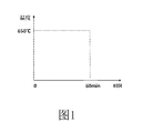
- FIG. 1 is a schematic diagram of an annealing process curve of the existing solid phase crystallization method. As shown in FIG.
- the conventional solid phase crystallization method is direct Amorphous silicon (a-Si: amorphous silicon) is placed in a high temperature environment of about 650 ° C for about 60 minutes for crystallization.
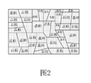
- Figure 2 is a schematic diagram of the morphology of the crystal grains obtained by the conventional solid phase crystallization method, as shown in Fig. 2.
- the amorphous silicon when the amorphous silicon is directly placed in a high temperature environment, the temperature of different regions of the amorphous silicon has a large difference in the initial stage of crystallization, and the growth rate of the crystal nucleus in different regions has a large difference.
- the grain size of the solid phase crystal is different, and the uniformity is poor, which ultimately leads to a large difference in characteristics of the TFT device, which affects the yield.
- An object of the present invention is to provide a solid phase crystallization method for reducing the difference in temperature of different regions when amorphous silicon starts to crystallize, thereby further reducing the difference in growth rate of crystal nuclei in different regions, and substantially improving the solidity.
- the uniformity of the crystal grains formed by the phase crystal is to provide a solid phase crystallization method for reducing the difference in temperature of different regions when amorphous silicon starts to crystallize, thereby further reducing the difference in growth rate of crystal nuclei in different regions, and substantially improving the solidity.
- Another object of the present invention is to provide a method for fabricating a low-temperature polysilicon TFT substrate.
- the solid phase crystallization method is used to crystallize amorphous silicon, which can improve the uniformity of the polycrystalline silicon crystal grains, thereby greatly improving the characteristics of the TFT device and improving the production. Yield.
- the present invention provides a solid phase crystallization method comprising: providing amorphous silicon, after heating the amorphous silicon to a first crystallization temperature, continuing heating the amorphous silicon to make it from the first time period
- the first crystallization temperature is gradually increased to the second crystallization temperature, and after the amorphous silicon is kept at the second crystallization temperature for a period of time, the amorphous silicon is cooled to gradually decrease from the second crystallization temperature to the second period in the second period.
- the amorphous silicon is continuously cooled down to room temperature to obtain low temperature polycrystalline silicon.
- the first crystallization temperature is 380-420 ° C and the second crystallization temperature is 630-670 ° C.
- the first period of time is the same as the length of the second period of time, both from 1 minute to 10 minutes, and the time during which the amorphous silicon is kept at the second crystallization temperature is 30 minutes to 120 minutes.
- the first time period and the second time period are both 5 minutes, and the time during which the amorphous silicon is kept at the second crystallization temperature is 60 minutes.
- the amorphous silicon is gradually heated from the first crystallization temperature to the second crystallization temperature at a constant heating rate, and gradually cooled from the second crystallization temperature to the first crystallization temperature at a constant temperature decreasing rate, the heating rate being the same as the cooling rate .
- the invention also provides a method for manufacturing a low temperature polysilicon TFT substrate, comprising the following steps:
- Step S1 providing a substrate, depositing a buffer layer on the substrate, depositing an amorphous silicon layer on the buffer layer, to obtain a substrate to be processed;
- Step S2 converting the amorphous silicon layer into a low-temperature polysilicon layer by a solid phase crystallization method, the solid phase crystallization method comprising: after heating the substrate to be processed to a first crystallization temperature, continuing to the substrate to be processed Heating, gradually increasing the temperature from the first crystallization temperature to the second crystallization temperature in the first period of time, and cooling the substrate to be treated after the substrate to be treated is kept at the second crystallization temperature for a period of time Decreasing the temperature from the second crystallization temperature to the first crystallization temperature in the second period of time, and continuing to cool the substrate to be treated to a room temperature;
- Step S3 performing patterning processing on the low temperature polysilicon layer to obtain an active layer
- Step S4 using a self-alignment technique to implant dopant ions at both ends of the active layer with the gate as a mask, forming a source contact region, a drain contact region, and a source contact region. Between the drain contact regions and corresponding to the channel region under the gate;
- Step S5 depositing an interlayer dielectric layer on the gate and gate insulating layer, and patterning the interlayer dielectric layer and the gate insulating layer, and the interlayer dielectric layer and the gate layer Source contact holes and drain contact holes respectively corresponding to the source contact region and the drain contact region of the active layer are formed in the insulating layer;
- Step S6 forming a source and a drain on the interlayer dielectric layer, wherein the source and the drain are in contact with the drain contact hole and the source contact region of the active layer and the drain through the source contact hole and the drain, respectively.
- the area is in contact.
- the first crystallization temperature is 380-420 ° C and the second crystallization temperature is 630-670 ° C.
- the first time period is the same as the length of the second time period, both of which are 1 minute to 10 minutes, and the time during which the substrate 40 to be processed is kept at the second crystallization temperature is 30 minutes to 120 minutes.
- the first time period and the second time period are both 5 minutes, and the substrate to be treated is kept at the second crystallization temperature for 60 minutes.
- the substrate to be processed is gradually heated from a first crystallization temperature to a second crystallization temperature at a constant heating rate, and gradually cooled from a second crystallization temperature to a first crystallization temperature at a constant temperature decreasing rate, the heating rate being the same as the cooling rate. .
- the present invention also provides a solid phase crystallization method comprising: providing amorphous silicon, heating the amorphous silicon to a first crystallization temperature, continuing to heat the amorphous silicon to be from the first crystallization temperature in the first period of time Gradually increasing the temperature to the second crystallization temperature, and after the amorphous silicon is kept at the second crystallization temperature for a period of time, the amorphous silicon is cooled to gradually decrease from the second crystallization temperature to the first crystallization temperature in the second period of time. The amorphous silicon continues to be cooled down to room temperature to obtain low temperature polysilicon;
- first crystallization temperature is 380-420 ° C
- second crystallization temperature is 630-670 ° C
- the first period of time is the same as the length of the second period of time, both being 5 minutes, and the time during which the amorphous silicon is kept at the second crystallization temperature is 60 minutes;
- the amorphous silicon is gradually heated from the first crystallization temperature to the second crystallization temperature at a constant temperature increase rate, and gradually cooled from the second crystallization temperature to the first crystallization temperature at a constant temperature drop rate, the temperature increase rate and the temperature decrease The rate is the same.
- the solid phase crystallization method of the present invention reduces the difference in temperature of different regions when amorphous silicon starts to crystallize, thereby reducing the difference in growth rate of crystal nuclei in different regions, and greatly improving the solidity.
- the method for fabricating the low-temperature polysilicon TFT substrate of the present invention uses the solid phase crystallization method to crystallize amorphous silicon, thereby improving the uniformity of the polycrystalline silicon crystal grains, thereby greatly improving the characteristics of the TFT device and improving the production yield.
- FIG. 1 is a schematic view showing an annealing process curve of a conventional solid phase crystallization method
- FIG. 2 is a schematic view showing the morphology of crystal grains obtained by the conventional solid phase crystallization method
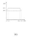
- FIG. 3 is a schematic view showing an annealing process curve of the solid phase crystallization method of the present invention.
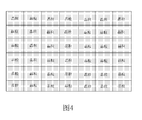
- FIG. 4 is a schematic view showing the morphology of crystal grains obtained by the solid phase crystallization method of the present invention.
- FIG. 5 is a flow chart of a method for fabricating a low temperature polysilicon TFT substrate of the present invention
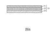
- FIG. 6 is a schematic view showing a step S1 of a method for fabricating a low-temperature polysilicon TFT substrate of the present invention
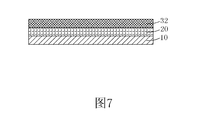
- step S2 is a schematic diagram of step S2 of the method for fabricating a low temperature polysilicon TFT substrate of the present invention
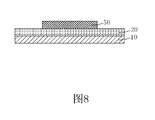
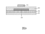
- FIG. 8 to FIG. 9 are schematic diagrams showing the step S3 of the method for fabricating the low temperature polysilicon TFT substrate of the present invention.
- step S4 of the method for fabricating a low temperature polysilicon TFT substrate of the present invention
- Figure 11 is a schematic view showing a step S5 of the method for fabricating a low temperature polysilicon TFT substrate of the present invention.
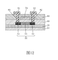
- Figure 12 is a schematic view showing a step S6 of the method for fabricating a low temperature polysilicon TFT substrate of the present invention.
- the present invention firstly provides a solid phase crystallization method comprising: providing amorphous silicon, heating the amorphous silicon to a first crystallization temperature, continuing to heat the amorphous silicon to be from the first crystallization temperature in the first period of time Gradually increasing the temperature to the second crystallization temperature, and after the amorphous silicon is kept at the second crystallization temperature for a period of time, the amorphous silicon is cooled to gradually decrease from the second crystallization temperature to the first crystallization temperature in the second period of time.
- the amorphous silicon is continuously cooled down to room temperature to obtain low temperature polycrystalline silicon.
- the first crystallization temperature is 380-420 ° C
- the second crystallization temperature is 630-670 ° C.
- the first crystallization temperature is 400 ° C and the second crystallization temperature is 650 ° C.
- the first time period is the same as the length of the second time period, both of which are 1 minute to 10 minutes, and the time during which the amorphous silicon is kept at the second crystallization temperature is 30 minutes to 120 minutes.
- the first time period and the second time period are both 5 minutes, and the amorphous silicon is kept at the second crystallization temperature for 60 minutes.
- the amorphous silicon is gradually heated from a first crystallization temperature to a second crystallization temperature at a constant heating rate, and gradually cooled from a second crystallization temperature to a first crystallization temperature at a constant temperature decreasing rate, the rate of temperature increase and The cooling rate is the same.
- the solid phase crystallization method of the present invention does not directly heat the amorphous silicon (a-Si) at a high temperature of about 650 ° C, but allows The crystallization temperature starts from a first crystallization temperature (preferably 400 ° C), gradually rises to a second crystallization temperature (preferably 650 ° C) over a first period of time (preferably 5 minutes), and is kept at a second crystallization temperature (preferably 650 ° C) for a period of time.
- a first crystallization temperature preferably 400 ° C
- a second crystallization temperature preferably 650 ° C
- a first period of time preferably 5 minutes
- the low-temperature polycrystalline silicon obtained by the solid phase crystallization method of the present invention has excellent uniformity of crystal grains, and when the low-temperature polycrystalline silicon is applied to a TFT device, the characteristics of the TFT device can be remarkably improved, and the production yield can be improved.
- the present invention further provides a method for fabricating a low-temperature polysilicon TFT substrate, wherein the amorphous silicon layer is crystallized by the solid phase crystallization method, and the method for fabricating the low-temperature polysilicon TFT substrate comprises the following steps:
- Step S1 as shown in FIG. 6, a base substrate 10 is provided, a buffer layer 20 is deposited on the base substrate 10, and an amorphous silicon layer 31 is deposited on the buffer layer 20 to obtain a substrate 40 to be processed.
- the base substrate 10 is a glass substrate.
- the buffer layer 20 and the amorphous silicon layer 31 are deposited by plasma enhanced chemical vapor deposition (PECVD).
- PECVD plasma enhanced chemical vapor deposition
- the buffer layer 20 comprises silicon nitride (SiN x) layer and a silicon nitride located (SiN x) on the base substrate 10 is a silicon oxide (SiO x) layer on the layer.
- Step S2 as shown in FIG. 7, the amorphous silicon layer 31 is converted into a low temperature polysilicon layer 32 by a solid phase crystallization method, and the solid phase crystallization method comprises: heating the substrate 40 to be processed to a first crystallization temperature. Afterwards, the substrate 40 to be processed is further heated to gradually increase the temperature from the first crystallization temperature to the second crystallization temperature in the first period of time, and after the substrate 40 to be processed is kept at the second crystallization temperature for a period of time, The substrate to be processed 40 is cooled to gradually decrease from the second crystallization temperature to the first crystallization temperature in the second period of time, and the substrate 40 to be processed is further cooled to be cooled to room temperature.
- the first crystallization temperature is 380-420 ° C
- the second crystallization temperature is 630-670 ° C.
- the first crystallization temperature is 400 ° C and the second crystallization temperature is 650 ° C.
- the first time period is the same as the length of the second time period, which is 1 minute to 10 minutes, and the time for the substrate 40 to be processed to be kept at the second crystallization temperature is 30 minutes to 120 minutes.
- the first time period and the second time period are both 5 minutes, and the time for the substrate 40 to be processed to be kept at the second crystallization temperature is 60 minutes.
- the substrate to be processed 40 is gradually heated from a first crystallization temperature to a second crystallization temperature at a constant temperature increase rate, and gradually cooled from a second crystallization temperature to a first crystallization temperature at a constant temperature drop rate, the temperature increase rate. Same as the cooling rate.
- the solid phase crystallization method of the step S2 does not directly heat the amorphous silicon (a-Si) at a high temperature of about 650 ° C for crystallization.
- the crystallization temperature is started from a first crystallization temperature (preferably 400 ° C), and the temperature is gradually increased to a second crystallization temperature (preferably 650 ° C) over a first period of time (preferably 5 minutes), and then at a second crystallization temperature (preferably 650 ° C).
- the temperature is maintained for a period of time (preferably 60 minutes), and then gradually lowered to a first crystallization temperature (preferably 400 ° C) over a second period of time (preferably 5 minutes); this allows the difference in temperature of different regions when the amorphous silicon layer 31 starts to crystallize.
- the decrease in properties further reduces the difference in the growth rate of crystal nuclei in different regions, and greatly improves the uniformity of crystal grains formed by solid phase crystals.
- the uniformity of the crystal grains of the low-temperature polysilicon layer 32 obtained by the solid phase crystallization method of the step S2 is extremely excellent, and the characteristics of the TFT device can be remarkably improved, and the production yield can be improved.
- Step S3 as shown in FIG. 8 and FIG. 9, patterning the low temperature polysilicon layer 32 to obtain an active layer 50; depositing a gate insulating layer 60 on the active layer 50 and the buffer layer 20, A gate electrode 70 is formed on the gate insulating layer 60.
- the gate insulating layer 60 is a silicon oxide (SiO x ) layer.
- the process of the gate 70 is: depositing a gate metal layer on the gate insulating layer 60 by using a physical vapor deposition method (PVD), and patterning the gate metal layer The treatment is performed to obtain the gate 70.
- PVD physical vapor deposition method
- the material of the gate 70 is metal molybdenum (Mo).
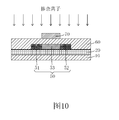
- Step S4 as shown in FIG. 10, using a self-alignment technique to implant dopant ions on both ends of the active layer 50 with the gate electrode 70 as a mask to form a source contact region 51 and a drain contact.
- a region 52 is located between the source contact region 51 and the drain contact region 52 and corresponds to the channel region 53 below the gate 70.
- the dopant ions are P-type ions
- the P-type ions are preferably boron (Boron) ions.
- Step S5 as shown in FIG. 11, an interlayer dielectric layer 80 is deposited on the gate electrode 70 and the gate insulating layer 60, and the interlayer dielectric layer 80 and the gate insulating layer 60 are patterned.
- a source contact hole 81 and a drain contact hole 82 respectively corresponding to the source contact region 51 and the drain contact region 52 of the active layer 50 are formed in the interlayer dielectric layer 80 and the gate insulating layer 60.
- the step S5 deposits an interlayer dielectric layer 80 on the gate electrode 70 and the gate insulating layer 60 by plasma enhanced chemical vapor deposition (PECVD).
- PECVD plasma enhanced chemical vapor deposition
- the interlayer dielectric layer 80 includes a silicon oxide (SiO x ) layer on the gate 70 and the gate insulating layer 60 and silicon nitride on the silicon oxide (SiO x ) layer ( SiN x ) layer.
- the step S5 further comprises: performing rapid thermal annealing (RTA) on the entire substrate of the inter-layer dielectric layer 80 before patterning the interlayer dielectric layer 80 to the active layer
- RTA rapid thermal annealing
- the activation is performed to cause the boron ions in the source contact region 51 and the drain contact region 52 to form a covalent bond with the polysilicon, thereby reducing the defects of the polysilicon and reducing the subsequently formed source 91 and the drain 92 and the active layer 50.
- the contact resistance enhances the electrical connection effect, and at the same time, the hydrogen in the silicon nitride (SiN x ) layer in the interlayer dielectric layer 80 is diffused into the active layer 50, and the polysilicon is supplemented with hydrogen to further reduce the polysilicon.
- the defects make the TFT work more stable.
- Step S6 as shown in FIG. 12, a source 91 and a drain 92 are formed on the interlayer dielectric layer 80.
- the source 91 and the drain 92 pass through the source contact hole 81 and the drain contact hole 82, respectively.
- the source contact region 51 of the active layer 50 is in contact with the drain contact region 52.
- the process of the source 91 and the drain 92 is: depositing a source/drain metal layer on the interlayer dielectric layer 80 by a physical vapor deposition method (PVD), The source and drain metal layers are patterned to obtain a source 91 and a drain 92.
- PVD physical vapor deposition method
- the source 91 and the drain 92 each include two first structural layers and a second structural layer interposed between the two first structural layers, and the first structural layer is made of molybdenum (Mo).
- the material of the second structural layer is aluminum (Al).
- the present invention provides a solid phase crystallization method and a method of fabricating a low temperature polysilicon TFT substrate.
- the solid phase crystallization method of the present invention comprises: providing amorphous silicon, heating the amorphous silicon to a first crystallization temperature, and continuing to heat the amorphous silicon to gradually increase the temperature from the first crystallization temperature to the first time period
- the second crystallization temperature after the amorphous silicon is kept at the second crystallization temperature for a period of time, the amorphous silicon is cooled, and gradually cooled from the second crystallization temperature to the first crystallization temperature in the second period, to the amorphous silicon Continue to cool down to room temperature to obtain low temperature polysilicon.
- the solid phase crystallization method reduces the difference in temperature of different regions when amorphous silicon starts to crystallize, thereby reducing the difference in growth rate of crystal nuclei in different regions, and substantially increasing the uniformity of crystal grains formed by solid phase crystals. Sex.
- the method for fabricating the low-temperature polysilicon TFT substrate of the present invention uses the solid phase crystallization method to crystallize amorphous silicon, thereby improving the uniformity of the polycrystalline silicon crystal grains, thereby greatly improving the characteristics of the TFT device and improving the production yield.
Landscapes
- Thin Film Transistor (AREA)
- Recrystallisation Techniques (AREA)
Abstract
一种固相结晶方法与低温多晶硅TFT基板的制作方法。上述固相结晶方法包括:提供非晶硅,将非晶硅加热至第一结晶温度后,对非晶硅继续加热,使其在第一时间段内从第一结晶温度逐渐升温至第二结晶温度,将非晶硅在第二结晶温度保温一段时间后,对非晶硅进行降温,使其在第二时间段内从第二结晶温度逐渐降温至第一结晶温度,对非晶硅继续降温,使其降至室温,得到低温多晶硅。该固相结晶方法能够提高多晶硅晶粒的均一性。上述低温多晶硅TFT基板的制作方法采用上述固相结晶方法对非晶硅进行结晶,能够提高多晶硅晶粒的均一性,改善TFT器件的特性。
Description
本发明涉及显示技术领域,尤其涉及一种固相结晶方法与低温多晶硅TFT基板的制作方法。
薄膜晶体管(Thin Film Transistor,简称TFT)是目前液晶显示装置(Liquid Crystal Display,简称LCD)和有源矩阵驱动式有机电致发光显示装置(Active Matrix/Organic Light-Emitting Diode,简称AMOLED)中的主要驱动元件,直接关系到高性能平板显示装置的发展方向。
低温多晶硅由于电子迁移率高,亚阈值摆幅好,开关态电流比大,耗电低,同时可以用于制作高像素密度(PPI)显示器,且可以应用在柔性OLED基板上,近几年引起了广泛的关注。对电压驱动式的液晶显示装置而言,低温多晶硅薄膜晶体管由于其具有较高的迁移率,可以使用体积较小的薄膜晶体管实现对液晶分子的偏转驱动,在很大程度上缩小了薄膜晶体管所占的体积,增加透光面积,得到更高的亮度和解析度;对于电流驱动式的有源矩阵驱动式有机电致发光显示装置而言,低温多晶硅薄膜晶体管可以更好的满足驱动电流要求。
目前,常见的低温多晶硅的晶化方法包括准分子激光退火(ELA,Excimer Laser Annealing)结晶方法与固相结晶(SPC,Solid Phase Crystallization)方法等。准分子激光退火结晶使用的机台昂贵,制作成本高,而且准分子激光退火结晶的晶粒均一性不好,制得的TFT基板用于显示器中时容易出现显示器亮度不均匀的问题(ELA scan mura),无法实现大尺寸显示面板的制作。与准分子激光退火结晶方法相比,固相结晶方法的制作成本较低,图1为现有的固相结晶方法的退火工艺曲线示意图,如图1所示,传统的固相结晶方法是直接将非晶硅(a-Si:amorphous silicon)置于650℃左右的高温环境中持续加热60min左右进行结晶,图2为现有的固相结晶方法制得的晶粒的形态示意图,如图2所示,由于将非晶硅直接放置于高温环境中时,在结晶初始阶段非晶硅不同区域的温度具有较大的差异性,进而使不同区域的晶核的成长速度具有较大的差异性,导致固相结晶形成的晶粒大小不一,均一性差,最终导致TFT器件特性的差异性大,影响良率。
发明内容
本发明的目的在于提供一种固相结晶方法,使非晶硅开始结晶时不同区域的温度的差异性减小,进而使不同区域的晶核的成长速度的差异性减小,大幅度提高固相结晶形成的晶粒的均一性。
本发明的目的还在于提供一种低温多晶硅TFT基板的制作方法,采用上述固相结晶方法对非晶硅进行结晶,能够提高多晶硅晶粒的均一性,从而大幅度改善TFT器件的特性,提高生产良率。
为实现上述目的,本发明提供一种固相结晶方法,包括:提供非晶硅,将非晶硅加热至第一结晶温度后,对非晶硅继续加热,使其在第一时间段内从第一结晶温度逐渐升温至第二结晶温度,将非晶硅在第二结晶温度保温一段时间后,对非晶硅进行降温,使其在第二时间段内从第二结晶温度逐渐降温至第一结晶温度,对非晶硅继续降温,使其降至室温,得到低温多晶硅。
所述第一结晶温度为380-420℃,所述第二结晶温度为630-670℃。
所述第一时间段与第二时间段长度相同,均为1分钟至10分钟,将非晶硅在第二结晶温度保温的时间为30分钟至120分钟。
所述第一时间段与第二时间段均为5分钟,将非晶硅在第二结晶温度保温的时间为60分钟。
所述非晶硅按照恒定的升温速率从第一结晶温度逐渐升温至第二结晶温度,并按照恒定的降温速率从第二结晶温度逐渐降温至第一结晶温度,所述升温速率与降温速率相同。
本发明还提供一种低温多晶硅TFT基板的制作方法,包括如下步骤:
步骤S1、提供衬底基板,在所述衬底基板上沉积缓冲层,在所述缓冲层上沉积非晶硅层,得到待处理基板;
步骤S2、采用固相结晶方法使所述非晶硅层转化为低温多晶硅层,所述固相结晶方法包括:将所述待处理基板加热至第一结晶温度后,对所述待处理基板继续加热,使其在第一时间段内从第一结晶温度逐渐升温至第二结晶温度,将所述待处理基板在第二结晶温度保温一段时间后,对所述待处理基板进行降温,使其在第二时间段内从第二结晶温度逐渐降温至第一结晶温度,对所述待处理基板继续降温,使其降至室温;
步骤S3、对所述低温多晶硅层进行图形化处理,得到有源层;
在所述有源层与缓冲层上沉积栅极绝缘层,在所述栅极绝缘层上形成栅极;
步骤S4、采用自对准技术以所述栅极为掩膜板在所述有源层的两端植入掺杂离子,形成源极接触区、漏极接触区以及位于所述源极接触区与漏极接触区之间且对应于所述栅极下方的沟道区;
步骤S5、在所述栅极与栅极绝缘层上沉积层间介电层,对所述层间介电层与栅极绝缘层进行图形化处理,在所述层间介电层与栅极绝缘层中形成分别对应于有源层的源极接触区与漏极接触区的源极接触孔与漏极接触孔;
步骤S6、在所述层间介电层上形成源极与漏极,所述源极与漏极分别通过源极接触孔与漏极接触孔和有源层的源极接触区与漏极接触区相接触。
所述第一结晶温度为380-420℃,所述第二结晶温度为630-670℃。
所述第一时间段与第二时间段长度相同,均为1分钟至10分钟,将所述待处理基板40在第二结晶温度保温的时间为30分钟至120分钟。
所述第一时间段与第二时间段均为5分钟,将所述待处理基板在第二结晶温度保温的时间为60分钟。
所述待处理基板按照恒定的升温速率从第一结晶温度逐渐升温至第二结晶温度,并按照恒定的降温速率从第二结晶温度逐渐降温至第一结晶温度,所述升温速率与降温速率相同。
本发明还提供一种固相结晶方法,包括:提供非晶硅,将非晶硅加热至第一结晶温度后,对非晶硅继续加热,使其在第一时间段内从第一结晶温度逐渐升温至第二结晶温度,将非晶硅在第二结晶温度保温一段时间后,对非晶硅进行降温,使其在第二时间段内从第二结晶温度逐渐降温至第一结晶温度,对非晶硅继续降温,使其降至室温,得到低温多晶硅;
其中,所述第一结晶温度为380-420℃,所述第二结晶温度为630-670℃;
其中,所述第一时间段与第二时间段长度相同,均为5分钟,将非晶硅在第二结晶温度保温的时间为60分钟;
其中,所述非晶硅按照恒定的升温速率从第一结晶温度逐渐升温至第二结晶温度,并按照恒定的降温速率从第二结晶温度逐渐降温至第一结晶温度,所述升温速率与降温速率相同。
本发明的有益效果:本发明的固相结晶方法使非晶硅开始结晶时不同区域的温度的差异性减小,进而使不同区域的晶核的成长速度的差异性减小,大幅度提高固相结晶形成的晶粒的均一性。本发明的低温多晶硅TFT基板的制作方法采用上述固相结晶方法对非晶硅进行结晶,能够提高多晶硅晶粒的均一性,从而大幅度改善TFT器件的特性,提高生产良率。
为了能更进一步了解本发明的特征以及技术内容,请参阅以下有关本 发明的详细说明与附图,然而附图仅提供参考与说明用,并非用来对本发明加以限制。
下面结合附图,通过对本发明的具体实施方式详细描述,将使本发明的技术方案及其它有益效果显而易见。
附图中,
图1为现有的固相结晶方法的退火工艺曲线示意图;
图2为现有的固相结晶方法制得的晶粒的形态示意图;
图3为本发明的固相结晶方法的退火工艺曲线示意图;
图4为本发明的固相结晶方法制得的晶粒的形态示意图;
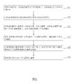
图5为本发明的低温多晶硅TFT基板的制作方法的流程图;
图6为本发明的低温多晶硅TFT基板的制作方法的步骤S1的示意图;
图7为本发明的低温多晶硅TFT基板的制作方法的步骤S2的示意图;
图8至图9为本发明的低温多晶硅TFT基板的制作方法的步骤S3的示意图;
图10为本发明的低温多晶硅TFT基板的制作方法的步骤S4的示意图;
图11为本发明的低温多晶硅TFT基板的制作方法的步骤S5的示意图;
图12为本发明的低温多晶硅TFT基板的制作方法的步骤S6的示意图。
为更进一步阐述本发明所采取的技术手段及其效果,以下结合本发明的优选实施例及其附图进行详细描述。
本发明首先提供一种固相结晶方法,包括:提供非晶硅,将非晶硅加热至第一结晶温度后,对非晶硅继续加热,使其在第一时间段内从第一结晶温度逐渐升温至第二结晶温度,将非晶硅在第二结晶温度保温一段时间后,对非晶硅进行降温,使其在第二时间段内从第二结晶温度逐渐降温至第一结晶温度,对非晶硅继续降温,使其降至室温,得到低温多晶硅。
具体的,所述第一结晶温度为380-420℃,所述第二结晶温度为630-670℃。
优选的,所述第一结晶温度为400℃,所述第二结晶温度为650℃。
具体的,所述第一时间段与第二时间段长度相同,均为1分钟至10分钟,将非晶硅在第二结晶温度保温的时间为30分钟至120分钟。
优选的,所述第一时间段与第二时间段均为5分钟,将非晶硅在第二 结晶温度保温的时间为60分钟。
优选的,所述非晶硅按照恒定的升温速率从第一结晶温度逐渐升温至第二结晶温度,并按照恒定的降温速率从第二结晶温度逐渐降温至第一结晶温度,所述升温速率与降温速率相同。
如图3所示,与现有的固相结晶方法相比,本发明的固相结晶方法不直接将非晶硅(a-Si)置于650℃左右的高温中加热进行结晶,而是让结晶温度从第一结晶温度(优选400℃)开始,经过第一时间段(优选5分钟)逐渐升温至第二结晶温度(优选650℃),再在第二结晶温度(优选650℃)保温一段时间(优选60分钟),然后经过第二时间段(优选5分钟)逐渐降温至第一结晶温度(优选400℃);这样可以使非晶硅开始结晶时不同区域的温度的差异性减小,进而使不同区域的晶核的成长速度的差异性减小,大幅度提高固相结晶形成的晶粒的均一性。如图4所示,本发明的固相结晶方法制得的低温多晶硅的晶粒的均一性非常优异,该低温多晶硅应用于TFT器件时,能够显著改善TFT器件的特性,提高生产良率。
请参阅图5,本发明还提供一种低温多晶硅TFT基板的制作方法,采用上述固相结晶方法对非晶硅层进行晶化处理,所述低温多晶硅TFT基板的制作方法包括如下步骤:
步骤S1、如图6所示,提供衬底基板10,在所述衬底基板10上沉积缓冲层20,在所述缓冲层20上沉积非晶硅层31,得到待处理基板40。
具体的,所述衬底基板10为玻璃基板。
具体的,所述步骤S1采用等离子体增强化学气相沉积法(PECVD,Plasma Enhanced Chemical Vapor Deposition)沉积缓冲层20与非晶硅层31。
具体的,所述缓冲层20包括位于所述衬底基板10上的氮化硅(SiN
x)层及位于所述氮化硅(SiN
x)层上的氧化硅(SiO
x)层。
步骤S2、如图7所示,采用固相结晶方法使所述非晶硅层31转化为低温多晶硅层32,所述固相结晶方法包括:将所述待处理基板40加热至第一结晶温度后,对所述待处理基板40继续加热,使其在第一时间段内从第一结晶温度逐渐升温至第二结晶温度,将所述待处理基板40在第二结晶温度保温一段时间后,对所述待处理基板40进行降温,使其在第二时间段内从第二结晶温度逐渐降温至第一结晶温度,对所述待处理基板40继续降温,使其降至室温。
具体的,所述第一结晶温度为380-420℃,所述第二结晶温度为630-670℃。
优选的,所述第一结晶温度为400℃,所述第二结晶温度为650℃。
具体的,所述第一时间段与第二时间段长度相同,均为1分钟至10分钟,将所述待处理基板40在第二结晶温度保温的时间为30分钟至120分钟。
优选的,所述第一时间段与第二时间段均为5分钟,将所述待处理基板40在第二结晶温度保温的时间为60分钟。
优选的,所述待处理基板40按照恒定的升温速率从第一结晶温度逐渐升温至第二结晶温度,并按照恒定的降温速率从第二结晶温度逐渐降温至第一结晶温度,所述升温速率与降温速率相同。
如图3所示,与现有的固相结晶方法相比,所述步骤S2的固相结晶方法不直接将非晶硅(a-Si)置于650℃左右的高温中加热进行结晶,而是让结晶温度从第一结晶温度(优选400℃)开始,经过第一时间段(优选5分钟)逐渐升温至第二结晶温度(优选650℃),再在第二结晶温度(优选650℃)保温一段时间(优选60分钟),然后经过第二时间段(优选5分钟)逐渐降温至第一结晶温度(优选400℃);这样可以使非晶硅层31开始结晶时不同区域的温度的差异性减小,进而使不同区域的晶核的成长速度的差异性减小,大幅度提高固相结晶形成的晶粒的均一性。如图4所示,所述步骤S2的固相结晶方法制得的低温多晶硅层32的晶粒的均一性非常优异,能够显著改善TFT器件的特性,提高生产良率。
步骤S3、如图8、图9所示,对所述低温多晶硅层32进行图形化处理,得到有源层50;在所述有源层50与缓冲层20上沉积栅极绝缘层60,在所述栅极绝缘层60上形成栅极70。
具体的,所述栅极绝缘层60为氧化硅(SiO
x)层。
具体的,所述步骤S3中,所述栅极70的制程为:采用物理气相沉积方法(PVD)在所述栅极绝缘层60上沉积栅极金属层,对所述栅极金属层进行图形化处理,得到栅极70。
具体的,所述栅极70的材料为金属钼(Mo)。
步骤S4、如图10所示,采用自对准技术以所述栅极70为掩膜板在所述有源层50的两端植入掺杂离子,形成源极接触区51、漏极接触区52以及位于所述源极接触区51与漏极接触区52之间且对应于所述栅极70下方的沟道区53。
具体的,所述掺杂离子为P型离子,所述P型离子优选为硼(Boron)离子。
步骤S5、如图11所示,在所述栅极70与栅极绝缘层60上沉积层间介电层80,对所述层间介电层80与栅极绝缘层60进行图形化处理,在所述 层间介电层80与栅极绝缘层60中形成分别对应于有源层50的源极接触区51与漏极接触区52的源极接触孔81与漏极接触孔82。
具体的,所述步骤S5采用等离子体增强化学气相沉积法(PECVD)在所述栅极70与栅极绝缘层60上沉积层间介电层80。
具体的,所述层间介电层80包括位于所述栅极70与栅极绝缘层60上的氧化硅(SiO
x)层及位于所述氧化硅(SiO
x)层上的氮化硅(SiN
x)层。
优选的,所述步骤S5还包括:对所述层间介电层80进行图形化处理之前,对附着层间介电层80的整个基板进行快速热退火处理(RTA),以对有源层50进行活化,使源极接触区51与漏极接触区52中的硼离子与多晶硅形成共价键,减少多晶硅的缺陷,降低后续形成的源极91和漏极92与有源层50之间的接触阻抗,提升电性连接效果,同时还能够使层间介电层80中的氮化硅(SiN
x)层中的氢扩散至有源层50中,对多晶硅进行补氢,进一步减少多晶硅的缺陷,使TFT工作更稳定。
步骤S6、如图12所示,在所述层间介电层80上形成源极91与漏极92,所述源极91与漏极92分别通过源极接触孔81与漏极接触孔82和有源层50的源极接触区51与漏极接触区52相接触。
具体的,所述步骤S6中,所述源极91与漏极92的制程为:采用物理气相沉积方法(PVD)在所述层间介电层80上沉积源漏极金属层,对所述源漏极金属层进行图形化处理,得到源极91与漏极92。
具体的,所述源极91与漏极92均包括两第一结构层及夹设于两第一结构层之间的第二结构层,所述第一结构层的材料为钼(Mo),所述第二结构层的材料为铝(Al)。
综上所述,本发明提供一种固相结晶方法与低温多晶硅TFT基板的制作方法。本发明的固相结晶方法包括:提供非晶硅,将非晶硅加热至第一结晶温度后,对非晶硅继续加热,使其在第一时间段内从第一结晶温度逐渐升温至第二结晶温度,将非晶硅在第二结晶温度保温一段时间后,对非晶硅进行降温,使其在第二时间段内从第二结晶温度逐渐降温至第一结晶温度,对非晶硅继续降温,使其降至室温,得到低温多晶硅。该固相结晶方法使非晶硅开始结晶时不同区域的温度的差异性减小,进而使不同区域的晶核的成长速度的差异性减小,大幅度提高固相结晶形成的晶粒的均一性。本发明的低温多晶硅TFT基板的制作方法采用上述固相结晶方法对非晶硅进行结晶,能够提高多晶硅晶粒的均一性,从而大幅度改善TFT器件的特性,提高生产良率。
以上所述,对于本领域的普通技术人员来说,可以根据本发明的技术 方案和技术构思作出其他各种相应的改变和变形,而所有这些改变和变形都应属于本发明权利要求的保护范围。
Claims (11)
- 一种固相结晶方法,包括:提供非晶硅,将非晶硅加热至第一结晶温度后,对非晶硅继续加热,使其在第一时间段内从第一结晶温度逐渐升温至第二结晶温度,将非晶硅在第二结晶温度保温一段时间后,对非晶硅进行降温,使其在第二时间段内从第二结晶温度逐渐降温至第一结晶温度,对非晶硅继续降温,使其降至室温,得到低温多晶硅。
- 如权利要求1所述的固相结晶方法,其中,所述第一结晶温度为380-420℃,所述第二结晶温度为630-670℃。
- 如权利要求1所述的固相结晶方法,其中,所述第一时间段与第二时间段长度相同,均为1分钟至10分钟,将非晶硅在第二结晶温度保温的时间为30分钟至120分钟。
- 如权利要求3所述的固相结晶方法,其中,所述第一时间段与第二时间段均为5分钟,将非晶硅在第二结晶温度保温的时间为60分钟。
- 如权利要求1所述的固相结晶方法,其中,所述非晶硅按照恒定的升温速率从第一结晶温度逐渐升温至第二结晶温度,并按照恒定的降温速率从第二结晶温度逐渐降温至第一结晶温度,所述升温速率与降温速率相同。
- 一种低温多晶硅TFT基板的制作方法,包括如下步骤:步骤S1、提供衬底基板,在所述衬底基板上沉积缓冲层,在所述缓冲层上沉积非晶硅层,得到待处理基板;步骤S2、采用固相结晶方法使所述非晶硅层转化为低温多晶硅层,所述固相结晶方法包括:将所述待处理基板加热至第一结晶温度后,对所述待处理基板继续加热,使其在第一时间段内从第一结晶温度逐渐升温至第二结晶温度,将所述待处理基板在第二结晶温度保温一段时间后,对所述待处理基板进行降温,使其在第二时间段内从第二结晶温度逐渐降温至第一结晶温度,对所述待处理基板继续降温,使其降至室温;步骤S3、对所述低温多晶硅层进行图形化处理,得到有源层;在所述有源层与缓冲层上沉积栅极绝缘层,在所述栅极绝缘层上形成栅极;步骤S4、采用自对准技术以所述栅极为掩膜板在所述有源层的两端植入掺杂离子,形成源极接触区、漏极接触区以及位于所述源极接触区与漏极接触区之间且对应于所述栅极下方的沟道区;步骤S5、在所述栅极与栅极绝缘层上沉积层间介电层,对所述层间介电层与栅极绝缘层进行图形化处理,在所述层间介电层与栅极绝缘层中形成分别对应于有源层的源极接触区与漏极接触区的源极接触孔与漏极接触孔;步骤S6、在所述层间介电层上形成源极与漏极,所述源极与漏极分别通过源极接触孔与漏极接触孔和有源层的源极接触区与漏极接触区相接触。
- 如权利要求6所述的低温多晶硅TFT基板的制作方法,其中,所述第一结晶温度为380-420℃,所述第二结晶温度为630-670℃。
- 如权利要求6所述的低温多晶硅TFT基板的制作方法,其中,所述第一时间段与第二时间段长度相同,均为1分钟至10分钟,将所述待处理基板40在第二结晶温度保温的时间为30分钟至120分钟。
- 如权利要求8所述的低温多晶硅TFT基板的制作方法,其中,所述第一时间段与第二时间段均为5分钟,将所述待处理基板在第二结晶温度保温的时间为60分钟。
- 如权利要求6所述的低温多晶硅TFT基板的制作方法,其中,所述待处理基板按照恒定的升温速率从第一结晶温度逐渐升温至第二结晶温度,并按照恒定的降温速率从第二结晶温度逐渐降温至第一结晶温度,所述升温速率与降温速率相同。
- 一种固相结晶方法,包括:提供非晶硅,将非晶硅加热至第一结晶温度后,对非晶硅继续加热,使其在第一时间段内从第一结晶温度逐渐升温至第二结晶温度,将非晶硅在第二结晶温度保温一段时间后,对非晶硅进行降温,使其在第二时间段内从第二结晶温度逐渐降温至第一结晶温度,对非晶硅继续降温,使其降至室温,得到低温多晶硅;其中,所述第一结晶温度为380-420℃,所述第二结晶温度为630-670℃;其中,所述第一时间段与第二时间段长度相同,均为5分钟,将非晶硅在第二结晶温度保温的时间为60分钟;其中,所述非晶硅按照恒定的升温速率从第一结晶温度逐渐升温至第二结晶温度,并按照恒定的降温速率从第二结晶温度逐渐降温至第一结晶温度,所述升温速率与降温速率相同。
Priority Applications (1)
| Application Number | Priority Date | Filing Date | Title |
|---|---|---|---|
| US15/773,690 US10515800B2 (en) | 2018-01-23 | 2018-02-22 | Solid phase crystallization method and manufacturing method of low-temperature poly-silicon TFT substrate |
Applications Claiming Priority (2)
| Application Number | Priority Date | Filing Date | Title |
|---|---|---|---|
| CN201810065170.6 | 2018-01-23 | ||
| CN201810065170.6A CN108281350B (zh) | 2018-01-23 | 2018-01-23 | 固相结晶方法与低温多晶硅tft基板的制作方法 |
Publications (1)
| Publication Number | Publication Date |
|---|---|
| WO2019144451A1 true WO2019144451A1 (zh) | 2019-08-01 |
Family
ID=62804660
Family Applications (1)
| Application Number | Title | Priority Date | Filing Date |
|---|---|---|---|
| PCT/CN2018/076942 Ceased WO2019144451A1 (zh) | 2018-01-23 | 2018-02-22 | 固相结晶方法与低温多晶硅tft基板的制作方法 |
Country Status (2)
| Country | Link |
|---|---|
| CN (1) | CN108281350B (zh) |
| WO (1) | WO2019144451A1 (zh) |
Citations (6)
| Publication number | Priority date | Publication date | Assignee | Title |
|---|---|---|---|---|
| US20020197742A1 (en) * | 2001-06-25 | 2002-12-26 | Kamins Theodore I. | Method of forming smooth polycrystalline silicon electrodes for molecular eletronic devices |
| KR20060040367A (ko) * | 2004-11-05 | 2006-05-10 | 엘지.필립스 엘시디 주식회사 | 자기장결정화방법에 의한 액정표시소자 제조방법 |
| US20070065998A1 (en) * | 2005-09-22 | 2007-03-22 | Si-Chen Lee | Polysilicon thin film fabrication method |
| CN102629558A (zh) * | 2012-01-09 | 2012-08-08 | 深超光电(深圳)有限公司 | 低温多晶硅薄膜晶体管制造方法 |
| CN102732941A (zh) * | 2012-05-30 | 2012-10-17 | 昆山工研院新型平板显示技术中心有限公司 | 一种低温多晶硅薄膜制造方法 |
| CN107369613A (zh) * | 2017-07-21 | 2017-11-21 | 京东方科技集团股份有限公司 | 多晶硅薄膜、薄膜晶体管的制作方法、设备、显示基板 |
Family Cites Families (4)
| Publication number | Priority date | Publication date | Assignee | Title |
|---|---|---|---|---|
| JPH06219723A (ja) * | 1993-01-25 | 1994-08-09 | Sony Corp | 結晶性半導体薄膜の製造方法 |
| CN101996869A (zh) * | 2009-08-31 | 2011-03-30 | 北大方正集团有限公司 | 多晶硅薄膜的制造方法及装置 |
| CN105097666B (zh) * | 2015-06-15 | 2017-12-01 | 深圳市华星光电技术有限公司 | 低温多晶硅tft基板的制作方法及低温多晶硅tft基板 |
| CN105097550A (zh) * | 2015-08-04 | 2015-11-25 | 深圳市华星光电技术有限公司 | 低温多晶硅薄膜晶体管的制作方法及低温多晶硅薄膜晶体管 |
-
2018
- 2018-01-23 CN CN201810065170.6A patent/CN108281350B/zh active Active
- 2018-02-22 WO PCT/CN2018/076942 patent/WO2019144451A1/zh not_active Ceased
Patent Citations (6)
| Publication number | Priority date | Publication date | Assignee | Title |
|---|---|---|---|---|
| US20020197742A1 (en) * | 2001-06-25 | 2002-12-26 | Kamins Theodore I. | Method of forming smooth polycrystalline silicon electrodes for molecular eletronic devices |
| KR20060040367A (ko) * | 2004-11-05 | 2006-05-10 | 엘지.필립스 엘시디 주식회사 | 자기장결정화방법에 의한 액정표시소자 제조방법 |
| US20070065998A1 (en) * | 2005-09-22 | 2007-03-22 | Si-Chen Lee | Polysilicon thin film fabrication method |
| CN102629558A (zh) * | 2012-01-09 | 2012-08-08 | 深超光电(深圳)有限公司 | 低温多晶硅薄膜晶体管制造方法 |
| CN102732941A (zh) * | 2012-05-30 | 2012-10-17 | 昆山工研院新型平板显示技术中心有限公司 | 一种低温多晶硅薄膜制造方法 |
| CN107369613A (zh) * | 2017-07-21 | 2017-11-21 | 京东方科技集团股份有限公司 | 多晶硅薄膜、薄膜晶体管的制作方法、设备、显示基板 |
Also Published As
| Publication number | Publication date |
|---|---|
| CN108281350B (zh) | 2020-09-01 |
| CN108281350A (zh) | 2018-07-13 |
Similar Documents
| Publication | Publication Date | Title |
|---|---|---|
| CN103985637B (zh) | 低温多晶硅薄膜晶体管及其制作方法和显示装置 | |
| CN106098628B (zh) | Tft背板的制作方法及tft背板 | |
| WO2016101392A1 (zh) | Amoled背板的制作方法及其结构 | |
| JP2009032757A (ja) | 薄膜半導体装置の製造方法 | |
| US10312273B2 (en) | Low temperature poly-silicon TFT substrate structure and manufacture method thereof | |
| CN105097667B (zh) | 低温多晶硅tft基板结构的制作方法及低温多晶硅tft基板结构 | |
| WO2015180450A1 (zh) | 低温多晶硅薄膜晶体管及其制备方法和显示器件 | |
| WO2016155056A1 (zh) | 低温多晶硅tft基板结构及其制作方法 | |
| CN104078621B (zh) | 低温多晶硅薄膜晶体管、其制备方法及阵列基板与显示装置 | |
| KR20110053039A (ko) | 다결정 실리콘층의 제조방법, 박막트랜지스터, 그를 포함하는 유기전계발광표시장치 및 그들의 제조방법 | |
| US10192903B2 (en) | Method for manufacturing TFT substrate | |
| US9356123B2 (en) | Manufacturing method of low temperature polycrystalline silicon thin film and manufacturing method of thin film transistor | |
| US7465614B2 (en) | Method of fabricating semiconductor device and semiconductor fabricated by the same method | |
| WO2016065768A1 (zh) | 低温多晶硅的制作方法及tft基板的制作方法 | |
| CN203895510U (zh) | 低温多晶硅薄膜晶体管及其阵列基板与显示装置 | |
| CN105489487A (zh) | 低温多晶硅薄膜及晶体管的制备方法、激光晶化装置 | |
| JP2007184562A (ja) | 多結晶シリコンフィルムの製造方法及びそれを適用した薄膜トランジスタの製造方法 | |
| CN105514035A (zh) | 低温多晶硅tft基板的制作方法及低温多晶硅tft基板 | |
| WO2020098143A1 (zh) | Oled 显示面板及其制作方法 | |
| CN108281350B (zh) | 固相结晶方法与低温多晶硅tft基板的制作方法 | |
| CN104599973A (zh) | 低温多晶硅薄膜晶体管的制备方法 | |
| US11521989B2 (en) | Display substrate, display apparatus and manufacturing method of display substrate | |
| US10515800B2 (en) | Solid phase crystallization method and manufacturing method of low-temperature poly-silicon TFT substrate | |
| KR100782769B1 (ko) | 정렬키, 정렬키 형성 방법 및 이를 이용한 레이저 결정화방법 | |
| KR100685428B1 (ko) | 박막트랜지스터의 제조방법 |
Legal Events
| Date | Code | Title | Description |
|---|---|---|---|
| 121 | Ep: the epo has been informed by wipo that ep was designated in this application |
Ref document number: 18901961 Country of ref document: EP Kind code of ref document: A1 |
|
| NENP | Non-entry into the national phase |
Ref country code: DE |
|
| 122 | Ep: pct application non-entry in european phase |
Ref document number: 18901961 Country of ref document: EP Kind code of ref document: A1 |