WO2019106979A1 - 処理装置 - Google Patents
処理装置 Download PDFInfo
- Publication number
- WO2019106979A1 WO2019106979A1 PCT/JP2018/038157 JP2018038157W WO2019106979A1 WO 2019106979 A1 WO2019106979 A1 WO 2019106979A1 JP 2018038157 W JP2018038157 W JP 2018038157W WO 2019106979 A1 WO2019106979 A1 WO 2019106979A1
- Authority
- WO
- WIPO (PCT)
- Prior art keywords
- substrate
- electrostatic chuck
- gas
- conductive member
- processing
- Prior art date
- Legal status (The legal status is an assumption and is not a legal conclusion. Google has not performed a legal analysis and makes no representation as to the accuracy of the status listed.)
- Ceased
Links
Images



Classifications
-
- B—PERFORMING OPERATIONS; TRANSPORTING
- B23—MACHINE TOOLS; METAL-WORKING NOT OTHERWISE PROVIDED FOR
- B23Q—DETAILS, COMPONENTS, OR ACCESSORIES FOR MACHINE TOOLS, e.g. ARRANGEMENTS FOR COPYING OR CONTROLLING; MACHINE TOOLS IN GENERAL CHARACTERISED BY THE CONSTRUCTION OF PARTICULAR DETAILS OR COMPONENTS; COMBINATIONS OR ASSOCIATIONS OF METAL-WORKING MACHINES, NOT DIRECTED TO A PARTICULAR RESULT
- B23Q3/00—Devices holding, supporting, or positioning work or tools, of a kind normally removable from the machine
- B23Q3/15—Devices for holding work using magnetic or electric force acting directly on the work
-
- C—CHEMISTRY; METALLURGY
- C23—COATING METALLIC MATERIAL; COATING MATERIAL WITH METALLIC MATERIAL; CHEMICAL SURFACE TREATMENT; DIFFUSION TREATMENT OF METALLIC MATERIAL; COATING BY VACUUM EVAPORATION, BY SPUTTERING, BY ION IMPLANTATION OR BY CHEMICAL VAPOUR DEPOSITION, IN GENERAL; INHIBITING CORROSION OF METALLIC MATERIAL OR INCRUSTATION IN GENERAL
- C23C—COATING METALLIC MATERIAL; COATING MATERIAL WITH METALLIC MATERIAL; SURFACE TREATMENT OF METALLIC MATERIAL BY DIFFUSION INTO THE SURFACE, BY CHEMICAL CONVERSION OR SUBSTITUTION; COATING BY VACUUM EVAPORATION, BY SPUTTERING, BY ION IMPLANTATION OR BY CHEMICAL VAPOUR DEPOSITION, IN GENERAL
- C23C16/00—Chemical coating by decomposition of gaseous compounds, without leaving reaction products of surface material in the coating, i.e. chemical vapour deposition [CVD] processes
- C23C16/06—Chemical coating by decomposition of gaseous compounds, without leaving reaction products of surface material in the coating, i.e. chemical vapour deposition [CVD] processes characterised by the deposition of metallic material
-
- C—CHEMISTRY; METALLURGY
- C23—COATING METALLIC MATERIAL; COATING MATERIAL WITH METALLIC MATERIAL; CHEMICAL SURFACE TREATMENT; DIFFUSION TREATMENT OF METALLIC MATERIAL; COATING BY VACUUM EVAPORATION, BY SPUTTERING, BY ION IMPLANTATION OR BY CHEMICAL VAPOUR DEPOSITION, IN GENERAL; INHIBITING CORROSION OF METALLIC MATERIAL OR INCRUSTATION IN GENERAL
- C23C—COATING METALLIC MATERIAL; COATING MATERIAL WITH METALLIC MATERIAL; SURFACE TREATMENT OF METALLIC MATERIAL BY DIFFUSION INTO THE SURFACE, BY CHEMICAL CONVERSION OR SUBSTITUTION; COATING BY VACUUM EVAPORATION, BY SPUTTERING, BY ION IMPLANTATION OR BY CHEMICAL VAPOUR DEPOSITION, IN GENERAL
- C23C16/00—Chemical coating by decomposition of gaseous compounds, without leaving reaction products of surface material in the coating, i.e. chemical vapour deposition [CVD] processes
- C23C16/44—Chemical coating by decomposition of gaseous compounds, without leaving reaction products of surface material in the coating, i.e. chemical vapour deposition [CVD] processes characterised by the method of coating
- C23C16/455—Chemical coating by decomposition of gaseous compounds, without leaving reaction products of surface material in the coating, i.e. chemical vapour deposition [CVD] processes characterised by the method of coating characterised by the method used for introducing gases into reaction chamber or for modifying gas flows in reaction chamber
- C23C16/45523—Pulsed gas flow or change of composition over time
- C23C16/45525—Atomic layer deposition [ALD]
- C23C16/45527—Atomic layer deposition [ALD] characterized by the ALD cycle, e.g. different flows or temperatures during half-reactions, unusual pulsing sequence, use of precursor mixtures or auxiliary reactants or activations
- C23C16/45536—Use of plasma, radiation or electromagnetic fields
- C23C16/45538—Plasma being used continuously during the ALD cycle
-
- C—CHEMISTRY; METALLURGY
- C23—COATING METALLIC MATERIAL; COATING MATERIAL WITH METALLIC MATERIAL; CHEMICAL SURFACE TREATMENT; DIFFUSION TREATMENT OF METALLIC MATERIAL; COATING BY VACUUM EVAPORATION, BY SPUTTERING, BY ION IMPLANTATION OR BY CHEMICAL VAPOUR DEPOSITION, IN GENERAL; INHIBITING CORROSION OF METALLIC MATERIAL OR INCRUSTATION IN GENERAL
- C23C—COATING METALLIC MATERIAL; COATING MATERIAL WITH METALLIC MATERIAL; SURFACE TREATMENT OF METALLIC MATERIAL BY DIFFUSION INTO THE SURFACE, BY CHEMICAL CONVERSION OR SUBSTITUTION; COATING BY VACUUM EVAPORATION, BY SPUTTERING, BY ION IMPLANTATION OR BY CHEMICAL VAPOUR DEPOSITION, IN GENERAL
- C23C16/00—Chemical coating by decomposition of gaseous compounds, without leaving reaction products of surface material in the coating, i.e. chemical vapour deposition [CVD] processes
- C23C16/44—Chemical coating by decomposition of gaseous compounds, without leaving reaction products of surface material in the coating, i.e. chemical vapour deposition [CVD] processes characterised by the method of coating
- C23C16/458—Chemical coating by decomposition of gaseous compounds, without leaving reaction products of surface material in the coating, i.e. chemical vapour deposition [CVD] processes characterised by the method of coating characterised by the method used for supporting substrates in the reaction chamber
-
- C—CHEMISTRY; METALLURGY
- C23—COATING METALLIC MATERIAL; COATING MATERIAL WITH METALLIC MATERIAL; CHEMICAL SURFACE TREATMENT; DIFFUSION TREATMENT OF METALLIC MATERIAL; COATING BY VACUUM EVAPORATION, BY SPUTTERING, BY ION IMPLANTATION OR BY CHEMICAL VAPOUR DEPOSITION, IN GENERAL; INHIBITING CORROSION OF METALLIC MATERIAL OR INCRUSTATION IN GENERAL
- C23C—COATING METALLIC MATERIAL; COATING MATERIAL WITH METALLIC MATERIAL; SURFACE TREATMENT OF METALLIC MATERIAL BY DIFFUSION INTO THE SURFACE, BY CHEMICAL CONVERSION OR SUBSTITUTION; COATING BY VACUUM EVAPORATION, BY SPUTTERING, BY ION IMPLANTATION OR BY CHEMICAL VAPOUR DEPOSITION, IN GENERAL
- C23C16/00—Chemical coating by decomposition of gaseous compounds, without leaving reaction products of surface material in the coating, i.e. chemical vapour deposition [CVD] processes
- C23C16/44—Chemical coating by decomposition of gaseous compounds, without leaving reaction products of surface material in the coating, i.e. chemical vapour deposition [CVD] processes characterised by the method of coating
- C23C16/458—Chemical coating by decomposition of gaseous compounds, without leaving reaction products of surface material in the coating, i.e. chemical vapour deposition [CVD] processes characterised by the method of coating characterised by the method used for supporting substrates in the reaction chamber
- C23C16/4582—Rigid and flat substrates, e.g. plates or discs
- C23C16/4583—Rigid and flat substrates, e.g. plates or discs the substrate being supported substantially horizontally
- C23C16/4585—Devices at or outside the perimeter of the substrate support, e.g. clamping rings, shrouds
-
- C—CHEMISTRY; METALLURGY
- C23—COATING METALLIC MATERIAL; COATING MATERIAL WITH METALLIC MATERIAL; CHEMICAL SURFACE TREATMENT; DIFFUSION TREATMENT OF METALLIC MATERIAL; COATING BY VACUUM EVAPORATION, BY SPUTTERING, BY ION IMPLANTATION OR BY CHEMICAL VAPOUR DEPOSITION, IN GENERAL; INHIBITING CORROSION OF METALLIC MATERIAL OR INCRUSTATION IN GENERAL
- C23C—COATING METALLIC MATERIAL; COATING MATERIAL WITH METALLIC MATERIAL; SURFACE TREATMENT OF METALLIC MATERIAL BY DIFFUSION INTO THE SURFACE, BY CHEMICAL CONVERSION OR SUBSTITUTION; COATING BY VACUUM EVAPORATION, BY SPUTTERING, BY ION IMPLANTATION OR BY CHEMICAL VAPOUR DEPOSITION, IN GENERAL
- C23C16/00—Chemical coating by decomposition of gaseous compounds, without leaving reaction products of surface material in the coating, i.e. chemical vapour deposition [CVD] processes
- C23C16/44—Chemical coating by decomposition of gaseous compounds, without leaving reaction products of surface material in the coating, i.e. chemical vapour deposition [CVD] processes characterised by the method of coating
- C23C16/458—Chemical coating by decomposition of gaseous compounds, without leaving reaction products of surface material in the coating, i.e. chemical vapour deposition [CVD] processes characterised by the method of coating characterised by the method used for supporting substrates in the reaction chamber
- C23C16/4582—Rigid and flat substrates, e.g. plates or discs
- C23C16/4583—Rigid and flat substrates, e.g. plates or discs the substrate being supported substantially horizontally
- C23C16/4586—Elements in the interior of the support, e.g. electrodes, heating or cooling devices
-
- H—ELECTRICITY
- H02—GENERATION; CONVERSION OR DISTRIBUTION OF ELECTRIC POWER
- H02N—ELECTRIC MACHINES NOT OTHERWISE PROVIDED FOR
- H02N13/00—Clutches or holding devices using electrostatic attraction, e.g. using Johnson-Rahbek effect
-
- H—ELECTRICITY
- H10—SEMICONDUCTOR DEVICES; ELECTRIC SOLID-STATE DEVICES NOT OTHERWISE PROVIDED FOR
- H10P—GENERIC PROCESSES OR APPARATUS FOR THE MANUFACTURE OR TREATMENT OF DEVICES COVERED BY CLASS H10
- H10P14/00—Formation of materials, e.g. in the shape of layers or pillars
- H10P14/40—Formation of materials, e.g. in the shape of layers or pillars of conductive or resistive materials
- H10P14/42—Formation of materials, e.g. in the shape of layers or pillars of conductive or resistive materials using a gas or vapour
-
- H—ELECTRICITY
- H10—SEMICONDUCTOR DEVICES; ELECTRIC SOLID-STATE DEVICES NOT OTHERWISE PROVIDED FOR
- H10P—GENERIC PROCESSES OR APPARATUS FOR THE MANUFACTURE OR TREATMENT OF DEVICES COVERED BY CLASS H10
- H10P14/00—Formation of materials, e.g. in the shape of layers or pillars
- H10P14/40—Formation of materials, e.g. in the shape of layers or pillars of conductive or resistive materials
- H10P14/42—Formation of materials, e.g. in the shape of layers or pillars of conductive or resistive materials using a gas or vapour
- H10P14/43—Chemical deposition, e.g. chemical vapour deposition [CVD]
-
- H—ELECTRICITY
- H10—SEMICONDUCTOR DEVICES; ELECTRIC SOLID-STATE DEVICES NOT OTHERWISE PROVIDED FOR
- H10P—GENERIC PROCESSES OR APPARATUS FOR THE MANUFACTURE OR TREATMENT OF DEVICES COVERED BY CLASS H10
- H10P14/00—Formation of materials, e.g. in the shape of layers or pillars
- H10P14/60—Formation of materials, e.g. in the shape of layers or pillars of insulating materials
-
- H—ELECTRICITY
- H10—SEMICONDUCTOR DEVICES; ELECTRIC SOLID-STATE DEVICES NOT OTHERWISE PROVIDED FOR
- H10P—GENERIC PROCESSES OR APPARATUS FOR THE MANUFACTURE OR TREATMENT OF DEVICES COVERED BY CLASS H10
- H10P72/00—Handling or holding of wafers, substrates or devices during manufacture or treatment thereof
- H10P72/04—Apparatus for manufacture or treatment
- H10P72/0431—Apparatus for thermal treatment
- H10P72/0432—Apparatus for thermal treatment mainly by conduction
-
- H—ELECTRICITY
- H10—SEMICONDUCTOR DEVICES; ELECTRIC SOLID-STATE DEVICES NOT OTHERWISE PROVIDED FOR
- H10P—GENERIC PROCESSES OR APPARATUS FOR THE MANUFACTURE OR TREATMENT OF DEVICES COVERED BY CLASS H10
- H10P72/00—Handling or holding of wafers, substrates or devices during manufacture or treatment thereof
- H10P72/70—Handling or holding of wafers, substrates or devices during manufacture or treatment thereof for supporting or gripping
- H10P72/72—Handling or holding of wafers, substrates or devices during manufacture or treatment thereof for supporting or gripping using electrostatic chucks
- H10P72/722—Details of electrostatic chucks
-
- H—ELECTRICITY
- H10—SEMICONDUCTOR DEVICES; ELECTRIC SOLID-STATE DEVICES NOT OTHERWISE PROVIDED FOR
- H10P—GENERIC PROCESSES OR APPARATUS FOR THE MANUFACTURE OR TREATMENT OF DEVICES COVERED BY CLASS H10
- H10P72/00—Handling or holding of wafers, substrates or devices during manufacture or treatment thereof
- H10P72/70—Handling or holding of wafers, substrates or devices during manufacture or treatment thereof for supporting or gripping
- H10P72/76—Handling or holding of wafers, substrates or devices during manufacture or treatment thereof for supporting or gripping using mechanical means, e.g. clamps or pinches
- H10P72/7604—Handling or holding of wafers, substrates or devices during manufacture or treatment thereof for supporting or gripping using mechanical means, e.g. clamps or pinches the wafers being placed on a susceptor, stage or support
- H10P72/7606—Handling or holding of wafers, substrates or devices during manufacture or treatment thereof for supporting or gripping using mechanical means, e.g. clamps or pinches the wafers being placed on a susceptor, stage or support characterised by edge clamping, e.g. clamping ring
-
- H—ELECTRICITY
- H10—SEMICONDUCTOR DEVICES; ELECTRIC SOLID-STATE DEVICES NOT OTHERWISE PROVIDED FOR
- H10P—GENERIC PROCESSES OR APPARATUS FOR THE MANUFACTURE OR TREATMENT OF DEVICES COVERED BY CLASS H10
- H10P72/00—Handling or holding of wafers, substrates or devices during manufacture or treatment thereof
- H10P72/70—Handling or holding of wafers, substrates or devices during manufacture or treatment thereof for supporting or gripping
- H10P72/76—Handling or holding of wafers, substrates or devices during manufacture or treatment thereof for supporting or gripping using mechanical means, e.g. clamps or pinches
- H10P72/7604—Handling or holding of wafers, substrates or devices during manufacture or treatment thereof for supporting or gripping using mechanical means, e.g. clamps or pinches the wafers being placed on a susceptor, stage or support
- H10P72/7612—Handling or holding of wafers, substrates or devices during manufacture or treatment thereof for supporting or gripping using mechanical means, e.g. clamps or pinches the wafers being placed on a susceptor, stage or support characterised by lifting arrangements, e.g. lift pins
Definitions
- the present invention relates to a technology for a processing apparatus that adsorbs a substrate by an electrostatic chuck to perform processing.
- film formation by chemical vapor deposition (CVD) or atomic layer deposition (ALD) is performed on a semiconductor wafer (hereinafter, referred to as a wafer) which is a substrate.
- CVD chemical vapor deposition
- ALD atomic layer deposition
- These film forming processes are performed by supplying a film forming gas in a state where the wafer mounted on the mounting table is heated to a predetermined temperature by a heater provided on the mounting table in the processing container.
- the film forming gas may be supplied in a state in which there is a possibility that the warpage will be further increased, or that there is a region where the temperature is not uniform in the plane of the wafer and does not reach the predetermined temperature in the plane of the wafer. There is a possibility that the film thickness may become uneven within the surface of the wafer.
- Patent Document 1 describes an apparatus for pressing a peripheral end portion of an LCD glass substrate to a mounting table by a pressing mechanism and performing adsorption by an electrostatic chuck when performing plasma etching. It is conceivable to apply this electrostatic chuck to a film forming apparatus in order to cope with the above-described wafer warpage problem.
- Patent Document 2 describes that an electrostatic chuck may be provided in a wafer film forming apparatus provided with a pressing mechanism similar to that of Patent Document 1.
- the electrostatic chuck disclosed in Patent Document 1 has a positive voltage and a negative voltage from a DC power supply as an electrode (chuck electrode) for polarizing a dielectric constituting a surface portion of the electrostatic chuck and adsorbing a substrate.
- a monopolar electrostatic chuck provided with only the electrode to which it is applied.
- plasma formed in the processing container is used as a conductive path so that the other of the positive voltage and the negative voltage is applied to the substrate from the above-described DC power supply. That is, in the atmosphere where plasma is not formed, the above polarization does not occur, and the substrate can not be adsorbed.
- the film formation process described above may be performed in an atmosphere in which no plasma is formed.
- an electrode to which a positive voltage is applied from a DC power supply and an electrode to which a negative voltage is applied from a DC power supply are provided as chuck electrodes so that the electrostatic chuck does not need to form the above plasma.
- a so-called bipolar electrostatic chuck is known. In Patent Document 2 described above, it is considered that this bipolar electrostatic chuck is provided because plasma is not formed in the processing container.
- the film forming gas supplied to the front surface of the wafer wraps around the back surface via the side of the wafer, and the film is formed in the gap between the back surface of the wafer and the electrostatic chuck.
- Patent Document 2 does not describe a method for solving this problem.
- the present invention has been made based on such circumstances, and its object is to adsorb a substrate with high certainty in processing the substrate in an atmosphere where no plasma is formed, and the uniformity is high in the surface of the substrate It is providing the technique which can process.
- a processing apparatus is provided in a processing container in which a vacuum atmosphere is formed, and includes an electrode, and an electrostatic chuck including a dielectric layer covering the electrode and the surface side forming an adsorption area of a substrate.
- a conductive member provided on the surface side of the dielectric layer; The electrostatic chuck is moved up and down relative to the conductive member such that the conductive member is positioned at a processing position where the conductive member contacts the substrate and a standby position for transporting the substrate to the electrostatic chuck.
- the positive electrode side is connected to one of the electrode and the conductive member, and the negative electrode side is connected to the other, and between the conductive member located at the processing position and the electrode in a state where plasma is not formed in the processing container
- a DC power supply for adsorbing the substrate to the dielectric layer by an electrostatic attraction force generated by applying a voltage A processing gas supply unit configured to supply a processing gas to the surface of the substrate in a state where the substrate is adsorbed to the dielectric layer; It is characterized by having.
- the positive electrode side and the negative electrode side of the DC power supply are respectively connected to one of the electrode and the conductive member constituting the electrostatic chuck, and the other to the other, and a voltage is generated between the electrode of the electrostatic chuck and the conductive member.
- a processing gas is supplied and processed in a state where the substrate is adsorbed to the electrostatic chuck by the electrostatic adsorption force generated thereby.
- the processing can be performed by reliably adsorbing the substrate to the electrostatic chuck with no plasma formed in the processing container. As a result, processing uniformity in the plane of the substrate can be enhanced.
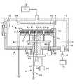
- the film-forming apparatus 1 which concerns on one embodiment of the processing apparatus of this invention is demonstrated with reference to the vertical side view of FIG.1 and FIG.2.
- the film forming apparatus 1 adsorbs a wafer W, which is a circular substrate made of silicon, for example, by an electrostatic chuck, and supplies a film forming gas while a clamp ring described later is in contact with the peripheral end of the wafer W. It is configured to perform CVD. By this CVD, a ruthenium (Ru) film, which is a metal film, is formed on the surface of the wafer W.
- ruthenium (Ru) film which is a metal film
- the film forming apparatus 1 includes a processing container 11, and no plasma is formed in the processing container 11.
- the processing container 11 is grounded to GND (ground).
- reference numeral 12 denotes a transfer port of the wafer W opened on the side wall of the processing container 11 and is opened and closed by the gate valve 13.
- An exhaust port 14 is opened at the bottom of the processing container 11 and is connected to a vacuum pump 16 through an exhaust pipe 15.
- reference 17 indicates a pressure adjusting unit constituted by a valve or the like interposed in the exhaust pipe 15 to adjust the exhaust amount from the exhaust port 14 and adjust the inside of the processing container 11 to a vacuum atmosphere of a desired pressure.
- the processing container 11 is provided with a horizontal and circular mounting table 2 for the wafer W.
- the surface portion (upper surface portion) of the mounting table 2 is configured by a flat circular electrostatic chuck 3.
- the electrostatic chuck 3 is described as a monopolar electrostatic chuck in the item of the problem to be solved by the invention.
- the electrostatic chuck 3 is configured of a main body 31 which is a dielectric and an electrode 32 embedded in the main body 31.
- the dielectric layer 30 is provided above the electrode 32 so as to cover the electrode 32.
- dielectric layers are provided below and to the sides of the electrodes 32.
- the wafer W is mounted on the surface of the electrostatic chuck 3 such that the center thereof overlaps with the center of the main body 31.
- the diameter of the main body portion 31 is formed larger than the diameter of the wafer W in order to suck the entire back surface of the wafer W placed thereon as described later.
- One end of the conductive wire 33 is connected to the electrode 32, and the other end of the conductive wire 33 extends downward in the column 21 of the mounting table 2, for example, via a switch 34 provided outside the processing container 11. It is connected to the positive electrode side of the DC power supply 35 provided outside the processing container 11. The negative electrode side of the DC power supply 35 is connected to the ground.
- a clamp ring 4 which is an annular member is provided on the upper side (surface side) of the electrostatic chuck 3.
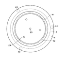
- the clamp ring 4 has a contact 42 at its inner end.
- the contact portion 42 is located slightly inside the peripheral end of the wafer W mounted on the electrostatic chuck 3 and is formed along the peripheral end of the wafer W in a plan view.
- the clamp ring 4 contacts the peripheral end of the wafer W by the contact portion 42 and plays a role of a conductive path for attracting the wafer W to the electrostatic chuck 3 as described later.
- the clamp ring 4 is constituted by a conductive member so as to function as a conductive path.
- a column 43 extends downward from the peripheral edge of the clamp ring 4.
- three columns 43 are provided, and they are provided at intervals in the circumferential direction of the clamp ring 4 so as not to prevent delivery of the wafer W to the electrostatic chuck 3.
- the lower end of the support column 43 is supported by the bottom surface of the processing container 11.
- the column 43 is configured as a conductive path.
- the electrostatic chuck 3 is configured to be able to move up and down.
- the electrostatic chuck 3 is at the standby position shown in FIG. Located at (conveying position).
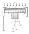
- the electrostatic chuck 3 is located at the processing position shown in FIG.
- the contact portion 42 of the clamp ring 4 is in contact with the peripheral edge of the wafer W over the entire periphery of the wafer W.
- the lower end of the column 43 is connected to the bottom of the processing vessel 11 and to the ground.
- the electrostatic chuck 3 described above is a Johnson-Labeck-type electrostatic chuck, and adsorbs the wafer W by the Johnson-Labeck force.
- the switch 34 is turned on, and a potential difference is formed between the electrode 32 of the electrostatic chuck 3 and the clamp ring 4.
- the Johnson-Labeck force of the electrostatic chuck 3 acts to attract the wafer W to the electrostatic chuck 3.
- the wafer W and the electrode 32 of the electrostatic chuck 3 function as an opposing electrode of the capacitor to polarize the entire surface with the dielectric layer 30 interposed therebetween. Adsorb the entire surface.
- the main body 31 has, for example, a volume resistivity of 1E 9 ⁇ ⁇ cm to 1E 11 ⁇ ⁇ cm in the temperature range in which the electrostatic chuck 3 is used. Is configured as.
- a heater 22 is embedded in the lower side of the electrostatic chuck 3 in the mounting table 2, and the surface of the electrostatic chuck 3 is heated to a desired temperature by the heater 22. Further, three elevating pins 23 are inserted into through holes 24 formed in the mounting table 2 so as to be opened in the surface of the electrostatic chuck 3.
- reference numeral 61 denotes a horizontal plate for supporting the raising and lowering pins 23, and reference numeral 45 in the drawing denotes a support rod whose upper end is connected to the horizontal plate 61. The lower end of the support rod 45 extends to the outside of the processing container 11 and is connected to the elevating mechanism 46.
- reference numeral 47 denotes a bellows which surrounds the support rod 45 at the outside of the processing container 11 and is provided so as to ensure the airtightness in the processing container 11.
- reference numeral 25 denotes a gas discharge hole opened at the center of the surface of the electrostatic chuck 3 and is connected to the gas supply source 26 via a gas supply passage provided in the mounting table 2 and the support 21.
- the gas supplied from the gas supply source 26 and discharged from the gas discharge hole 25 is a gas for transferring the heat of the electrostatic chuck 3 heated by the heater 22 to the wafer W, for example, He (helium) gas It is.
- the He gas discharged from the gas discharge holes 25 may be described as a heat transfer gas.
- the support 21 supporting the mounting table 2 is supported on a lift 63 provided on the outside of the processing container 11 via a through hole opened in the bottom surface of the processing container 11.
- the lifting platform 63 is configured to be lifted and lowered by a lifting mechanism 64. That is, in the film forming apparatus 1, the mounting table 2 is configured to be movable up and down.
- reference numeral 65 denotes a bellows, which is provided to surround the lower end portion of the support 21 supporting the mounting table 2 and to keep the inside of the processing container 11 airtight.
- a film forming gas supply unit 28 which is a processing gas supply unit for supplying a film forming gas as a processing gas into the processing container 11, is provided on the ceiling of the processing container 11 so as to face the mounting table 2.
- reference numeral 29 denotes a film forming gas supply source, which supplies a gas containing, for example, ruthenium carbonyl [Ru 3 (CO) 12 ] as a film forming gas for forming a Ru film to the film forming gas supply unit.
- the film forming apparatus 1 further includes a control unit 10.
- the control unit 10 is configured by a computer, and includes a program, a memory, and a CPU.
- the program incorporates steps so that a series of operations described later in the film forming apparatus 1 can be performed.
- the control unit 10 outputs a control signal to each unit of the film forming apparatus 1 according to the program, and the operation of each unit is controlled.
- each gas from the film forming gas supply source 29 and the heat transfer gas supply source 26 adjustment of the pressure in the processing container 11 by the pressure adjusting unit 17, elevation of the mounting table 2 by the elevation mechanism 64, elevation Control signals control operations such as raising and lowering of the raising and lowering pins 23 by the mechanism 46, adjustment of the temperature of the wafer W by adjusting the amount of heat generation of the heater 22, and on / off of the switch 34.
- the above program is stored in a storage medium such as, for example, a compact disk, a hard disk, a magneto-optical disk, or a DVD, and installed in the control unit 10.
- the wafer W is mounted on the electrostatic chuck 3 located at the standby position shown in FIG.
- the electrostatic chuck 3 moves to the processing position shown in FIG. 2 and the clamp ring 4 is in contact with the wafer W and the switch 34 is turned on, whereby the wafer W is attracted to the electrostatic chuck 3.
- heat is conducted from the electrostatic chuck 3 heated by the heater 22 to the wafer W.
- the heat transfer gas is discharged from the gas discharge holes 25 of the electrostatic chuck 3 to the back surface of the wafer W, and flows in a minute gap between the back surface of the wafer W and the electrostatic chuck 3.
- the heat of the electrostatic chuck 3 is also conducted to the wafer W through the heat transfer gas.
- the entire back surface of the wafer W is attracted to the electrostatic chuck 3 and is filled with the heat transfer gas, so the surface of the wafer W is uniformly heated. As a result, the temperature can be raised with high uniformity at each part in the plane of the wafer W.
- a film forming gas is supplied from the film forming gas supply unit 28, ruthenium carbonyl that constitutes the film forming gas is thermally decomposed on the surface of the wafer W, and a Ru film is formed on the surface of the wafer W.
- the film formation process of the Ru film is performed with the pressure in the processing container 11 relatively low.
- the heat of the mounting table is not easily transferred to the wafer W.
- the configuration of the wafer adsorption, the heat transfer gas, and the clamp ring by the above-described film forming apparatus 1 has an advantage that film formation can be performed with the temperature of the wafer W set to a desired temperature more reliably.
- the supply of the film forming gas from the film forming gas supply unit 28 and the discharge of the heat transfer gas from the gas discharge holes 25 are respectively stopped, and the film forming process is completed. Is carried out of the processing container 11 in a procedure reverse to the procedure performed at the time of loading into the processing container 11.
- the electrostatic chuck 3 for mounting the back surface of the wafer W, and the electrodes 32 constituting the clamp ring 4 in contact with the surface side of the peripheral end of the wafer W Are connected to each other.
- the wafer W is attracted to the electrostatic chuck 3 in an atmosphere where no plasma is formed due to the electrostatic attraction force generated by applying a voltage between the electrodes 32 and the clamp ring 4.
- the wafer W is heated so as to increase the uniformity of the temperature in the plane of the wafer W, so that the Ru film is formed with a film thickness with high uniformity in the plane.
- the yield of semiconductor products manufactured from the wafer W can be improved.
- the processing position of the clamp ring 4 when processing the wafer W may be any position that contacts the wafer W, and may be a position that contacts and presses the wafer W.
- the peripheral end of the wafer W is reliably brought into contact with the electrostatic chuck 3 by the pressing force and the suction action of the electrostatic chuck 3, and is heated by the heater 22. Heat is transferred from the electrostatic chuck 3. That is, the peripheral end of the wafer W can be more reliably prevented from rising from the electrostatic chuck 3, and the temperature decrease of the peripheral end can be suppressed.
- FIG. 5 shows an example in which one end of the flow path 53 is opened below the clamp ring 4 and on the peripheral end of the electrostatic chuck 3.
- the other end of the flow path 53 is connected to a CO gas supply source 54 that supplies, for example, CO (carbon monoxide) gas as a film formation suppression gas.
- CO carbon monoxide
- the film formation suppression gas supplied via the flow path 53 on the peripheral end of the electrostatic chuck 3 below the clamp ring 4 forms a film at a portion where the wafer W contacts the contact portion 42 of the clamp ring 4. It can be suppressed.
- a film forming apparatus 6 which is a modification of the film forming apparatus 1 will be described with reference to FIG. 6, focusing on differences from the film forming apparatus 1.
- the lower end of the column 43 supporting the clamp ring 4 is supported on the outer edge of a horizontal annular lower ring member 44 provided so as to surround the column 21 supporting the mounting table 2.
- the inner edge of the lower ring member 44 is located below the peripheral edge of the mounting table 2.
- the lower ring member 44 is also configured as a conductive path.
- the lower ring member 44 is connected to the lifting mechanism 46 via a support rod 45.
- the raising and lowering pins 23 are supported by the lower ring member 44 instead of being supported by the support plate 61. Accordingly, the clamp ring 4 and the raising and lowering pins 23 are raised and lowered together by the raising and lowering mechanism 46.
- the clamp ring 4 is raised and lowered between a position shown by a solid line in the figure and a position shown by a chain line.
- the position shown by the solid line is the position where the clamp ring 4 contacts the wafer W and the wafer W is attracted to the electrostatic chuck 3, and the electrostatic chuck 3 is seen from the clamp ring 4 by the description of the film forming apparatus 1. It will be located in the processing position mentioned.
- the position indicated by the broken line is the position of the clamp ring 4 when the wafer W is delivered between the transfer mechanism and the lift pins 23.
- the electrostatic chuck 3 has already been described as viewed from the clamp ring 4. It will be located at the standby position.
- the electrostatic chuck 3 may move up and down relative to the clamp ring 4, and either of the electrostatic chuck 3 and the clamp ring 4 may move up and down.
- the clamp ring 4 may be electrically connected to the DC power supply 34 and the ground, and the conductive path for making this connection may be formed by the support column 43 or the lower ring member 44. It is not limited.
- the film formed by the film forming gas by the film forming apparatus 1 is not limited to Ru, and can be used also when forming a conductive film having another conductivity.
- This conductive film is a film other than the insulating film, and includes a metal film.
- a metal film such as Cu (copper), Ti (titanium), W (tungsten), Al (aluminum) or the like can be formed.
- the conductive film includes a semiconductor film such as Si (silicon) or a film having conductivity such as carbon.
- any film forming apparatus may be used as long as the film forming gas is supplied to the substrate in an atmosphere in which plasma is not formed and the film forming is performed on the substrate.
- the present invention is not limited to an apparatus for forming a film by CVD, and configured as an apparatus for forming a film on a substrate by ALD by alternately and repeatedly supplying a source gas and a reaction gas that reacts with the source gas into the processing container 11. It may be done. Specifically, for example, a TiCl 4 (titanium tetrachloride) gas as a source gas and an NH 3 (ammonia) gas as a reaction gas may be supplied to form a TiN (titanium nitride) film by ALD. Good. As described above, in the film forming apparatus 1, the entire back surface of the wafer W is adsorbed, and the heat transfer gas flows below it.
- the conductive film is not easily formed on the back surface of the wafer W, and the loss of the attraction force of the wafer W is suppressed by the film formation of the conductive film.
- the film forming apparatus 1 can also be applied when forming an insulating film such as SiO 2 (silicon oxide) on the wafer W.
- the processing apparatus of the present technology is not limited to being configured as a film forming apparatus, and may be configured as, for example, an etching apparatus that supplies etching gas as a processing gas to the wafer W to perform etching.
- the conductive member provided on the surface side of the electrostatic chuck 3 is the clamp ring 4, ie, an annular member, but the conductive member is in contact with the wafer W in an atmosphere where plasma is not formed as described above. So long as the electrostatic attraction force can be generated. That is, the conductive member can have any shape, and is not limited to being annular.
- the potential difference may be formed between the clamp ring 4 and the electrode 32 of the electrostatic chuck 3 for the electrostatic chuck 3 to be energized, so that the positive electrode and the negative electrode of the DC power supply 35 are not connected to ground. It is included in the scope of Note that the present invention is not limited to the configuration examples described above, and the above-described embodiments can be appropriately modified or combined.
Landscapes
- Chemical & Material Sciences (AREA)
- Engineering & Computer Science (AREA)
- Mechanical Engineering (AREA)
- General Chemical & Material Sciences (AREA)
- Chemical Kinetics & Catalysis (AREA)
- Metallurgy (AREA)
- Materials Engineering (AREA)
- Organic Chemistry (AREA)
- Physics & Mathematics (AREA)
- Electromagnetism (AREA)
- Plasma & Fusion (AREA)
- Container, Conveyance, Adherence, Positioning, Of Wafer (AREA)
- Chemical Vapour Deposition (AREA)
Abstract
Description
前記誘電体層の表面側に設けられる導電部材と、
前記導電部材が前記基板に接触する処理位置と、前記静電チャックに基板を搬送するための待機位置とに各々位置するように、前記静電チャックを当該導電部材に対して相対的に昇降させる昇降機構と、
前記電極及び前記導電部材のうちの一方に正極側が、他方に負極側が各々接続され、前記処理容器内にプラズマが形成されていない状態で前記処理位置に位置する導電部材と前記電極との間に電圧が印加されて生じる静電吸着力により前記基板を前記誘電体層に吸着させるための直流電源と、
前記誘電体層に前記基板が吸着された状態で、当該基板の表面に処理ガスを供給して処理する処理ガス供給部と、
を備えたことを特徴とする。
また、載置台2を支持する支柱21は処理容器11の底面に開口した貫通孔を介して処理容器11の外側に設けられた昇降台63上に支持されている。昇降台63は昇降機構64により昇降自在に構成されている。つまり、この成膜装置1では載置台2が昇降自在に構成されている。図中65はベローズであり、載置台2を支持する支柱21の下端部を囲み、処理容器11内の気密性を保つために設けられる。
1 成膜装置
10 制御部
11 処理容器
2 載置台
28 成膜ガス供給部
3 静電チャック
31 電極
32 本体部
35 直流電源
4 クランプリング
Claims (7)
- 真空雰囲気が形成される処理容器内に設けられ、電極と、当該電極を覆うと共に表面側が基板の吸着領域をなす誘電体層と、を含む静電チャックと、
前記誘電体層の表面側に設けられる導電部材と、
前記導電部材が前記基板に接触する処理位置と、前記静電チャックに基板を搬送するための待機位置とに各々位置するように、前記静電チャックを当該導電部材に対して相対的に昇降させる昇降機構と、
前記電極及び前記導電部材のうちの一方に正極側が、他方に負極側が各々接続され、前記処理容器内にプラズマが形成されていない状態で前記処理位置に位置する導電部材と前記電極との間に電圧が印加されて生じる静電吸着力により前記基板を前記誘電体層に吸着させるための直流電源と、
前記誘電体層に前記基板が吸着された状態で、当該基板の表面に処理ガスを供給して処理する処理ガス供給部と、
を備えた処理装置。 - 前記導電部材は、内縁部が前記基板の周端部に沿って形成される環状部材である請求項1記載の処理装置。
- 前記処理ガスは、前記基板に成膜するための成膜ガスである請求項1記載の処理装置。
- 前記成膜ガスは、前記基板に導電膜を成膜するためのガスである請求項3記載の処理装置
- 前記処理位置は、前記導電部材により前記基板の周端部が前記静電チャックに接触し、且つ押圧される位置である請求項1記載の処理装置。
- 前記電極として、前記直流電源の正極側及び負極側のうちいずれか一方に接続される電極のみを備える請求項1記載の処理装置。
- 前記導電部材と前記基板との間の成膜を抑制するために、導電部材の下方で静電チャックの周端部上に成膜抑制ガスを供給するガス吐出部が設けられる請求項3記載の処理装置。
Priority Applications (4)
| Application Number | Priority Date | Filing Date | Title |
|---|---|---|---|
| CN201880074074.6A CN111417742B (zh) | 2017-11-28 | 2018-10-12 | 处理装置 |
| KR1020207017505A KR102548233B1 (ko) | 2017-11-28 | 2018-10-12 | 처리 장치 |
| US16/767,480 US20210005493A1 (en) | 2017-11-28 | 2018-10-12 | Processing apparatus |
| JP2019557054A JP7103372B2 (ja) | 2017-11-28 | 2018-10-12 | 処理装置 |
Applications Claiming Priority (2)
| Application Number | Priority Date | Filing Date | Title |
|---|---|---|---|
| JP2017-228011 | 2017-11-28 | ||
| JP2017228011 | 2017-11-28 |
Publications (1)
| Publication Number | Publication Date |
|---|---|
| WO2019106979A1 true WO2019106979A1 (ja) | 2019-06-06 |
Family
ID=66663999
Family Applications (1)
| Application Number | Title | Priority Date | Filing Date |
|---|---|---|---|
| PCT/JP2018/038157 Ceased WO2019106979A1 (ja) | 2017-11-28 | 2018-10-12 | 処理装置 |
Country Status (6)
| Country | Link |
|---|---|
| US (1) | US20210005493A1 (ja) |
| JP (1) | JP7103372B2 (ja) |
| KR (1) | KR102548233B1 (ja) |
| CN (1) | CN111417742B (ja) |
| TW (1) | TWI799472B (ja) |
| WO (1) | WO2019106979A1 (ja) |
Cited By (2)
| Publication number | Priority date | Publication date | Assignee | Title |
|---|---|---|---|---|
| JP2021197459A (ja) * | 2020-06-15 | 2021-12-27 | 日新イオン機器株式会社 | ウエハ離脱装置及びウエハ離脱方法 |
| US20220199363A1 (en) * | 2020-12-23 | 2022-06-23 | Tokyo Electron Limited | Plasma processing apparatus and plasma processing method |
Families Citing this family (4)
| Publication number | Priority date | Publication date | Assignee | Title |
|---|---|---|---|---|
| US11282729B2 (en) * | 2018-12-27 | 2022-03-22 | Areesys Technologies, Inc. | Method and apparatus for poling polymer thin films |
| US11232971B2 (en) * | 2019-12-18 | 2022-01-25 | Taiwan Semiconductor Manufacturing Company, Ltd. | Workpiece holding mechanism, process system and manufacturing method of semiconductor structure |
| CN115394877B (zh) * | 2022-08-25 | 2025-08-26 | 北京北方华创微电子装备有限公司 | 一种晶片承载装置及半导体处理设备 |
| US20250343067A1 (en) * | 2024-05-01 | 2025-11-06 | Applied Materials, Inc. | Volume reduction in semiconductor processing chamber |
Citations (3)
| Publication number | Priority date | Publication date | Assignee | Title |
|---|---|---|---|---|
| JPH0513558A (ja) * | 1990-12-25 | 1993-01-22 | Ngk Insulators Ltd | ウエハー加熱装置及びその製造方法 |
| JPH09104986A (ja) * | 1992-06-24 | 1997-04-22 | Anelva Corp | 基板処理方法及びcvd処理方法 |
| JP2006518930A (ja) * | 2003-01-13 | 2006-08-17 | ウナクシス・バルツァース・アクティエンゲゼルシャフト | 基板処理設備 |
Family Cites Families (17)
| Publication number | Priority date | Publication date | Assignee | Title |
|---|---|---|---|---|
| JPS4839294B1 (ja) * | 1967-05-25 | 1973-11-22 | ||
| JPS5528394B2 (ja) * | 1973-12-26 | 1980-07-28 | ||
| JPS5183043A (en) * | 1975-01-18 | 1976-07-21 | Kobe Steel Ltd | Netsukanatsuensenzaino reikyakuhoho narabini sonosochi |
| JP2603909B2 (ja) * | 1992-06-24 | 1997-04-23 | アネルバ株式会社 | Cvd装置、マルチチャンバ方式cvd装置及びその基板処理方法 |
| JP3599204B2 (ja) * | 1995-06-08 | 2004-12-08 | アネルバ株式会社 | Cvd装置 |
| JP2001053030A (ja) * | 1999-08-11 | 2001-02-23 | Tokyo Electron Ltd | 成膜装置 |
| JP4422295B2 (ja) * | 2000-05-17 | 2010-02-24 | キヤノンアネルバ株式会社 | Cvd装置 |
| JP3880896B2 (ja) | 2002-07-16 | 2007-02-14 | 東京エレクトロン株式会社 | プラズマ処理装置およびプラズマ処理方法 |
| JP4839294B2 (ja) * | 2007-10-04 | 2011-12-21 | 株式会社アルバック | 半導体ウエハ保持装置 |
| KR101210210B1 (ko) * | 2008-08-05 | 2012-12-07 | 도쿄엘렉트론가부시키가이샤 | 배치대 구조, 성막 장치 및 성막 방법 |
| JP5554525B2 (ja) * | 2009-08-25 | 2014-07-23 | 日本特殊陶業株式会社 | 静電チャック |
| JP5528394B2 (ja) * | 2011-05-30 | 2014-06-25 | パナソニック株式会社 | プラズマ処理装置、搬送キャリア、及びプラズマ処理方法 |
| JP6056403B2 (ja) * | 2012-11-15 | 2017-01-11 | 東京エレクトロン株式会社 | 成膜装置 |
| JP6010433B2 (ja) * | 2012-11-15 | 2016-10-19 | 東京エレクトロン株式会社 | 基板載置台および基板処理装置 |
| US10153190B2 (en) * | 2014-02-05 | 2018-12-11 | Micron Technology, Inc. | Devices, systems and methods for electrostatic force enhanced semiconductor bonding |
| CN105568244B (zh) * | 2014-10-14 | 2018-07-06 | 北京北方华创微电子装备有限公司 | 一种物理气相沉积方法 |
| CN106158717B (zh) * | 2015-03-31 | 2019-08-23 | 北京北方华创微电子装备有限公司 | 机械卡盘及半导体加工设备 |
-
2018
- 2018-10-12 JP JP2019557054A patent/JP7103372B2/ja active Active
- 2018-10-12 US US16/767,480 patent/US20210005493A1/en not_active Abandoned
- 2018-10-12 WO PCT/JP2018/038157 patent/WO2019106979A1/ja not_active Ceased
- 2018-10-12 KR KR1020207017505A patent/KR102548233B1/ko active Active
- 2018-10-12 CN CN201880074074.6A patent/CN111417742B/zh active Active
- 2018-11-26 TW TW107142010A patent/TWI799472B/zh active
Patent Citations (3)
| Publication number | Priority date | Publication date | Assignee | Title |
|---|---|---|---|---|
| JPH0513558A (ja) * | 1990-12-25 | 1993-01-22 | Ngk Insulators Ltd | ウエハー加熱装置及びその製造方法 |
| JPH09104986A (ja) * | 1992-06-24 | 1997-04-22 | Anelva Corp | 基板処理方法及びcvd処理方法 |
| JP2006518930A (ja) * | 2003-01-13 | 2006-08-17 | ウナクシス・バルツァース・アクティエンゲゼルシャフト | 基板処理設備 |
Cited By (3)
| Publication number | Priority date | Publication date | Assignee | Title |
|---|---|---|---|---|
| JP2021197459A (ja) * | 2020-06-15 | 2021-12-27 | 日新イオン機器株式会社 | ウエハ離脱装置及びウエハ離脱方法 |
| US11476148B2 (en) | 2020-06-15 | 2022-10-18 | Nissin Ion Equipment Co., Ltd. | Wafer separating apparatus, and wafer separating method |
| US20220199363A1 (en) * | 2020-12-23 | 2022-06-23 | Tokyo Electron Limited | Plasma processing apparatus and plasma processing method |
Also Published As
| Publication number | Publication date |
|---|---|
| KR102548233B1 (ko) | 2023-06-27 |
| JP7103372B2 (ja) | 2022-07-20 |
| KR20200083612A (ko) | 2020-07-08 |
| CN111417742A (zh) | 2020-07-14 |
| TW201933443A (zh) | 2019-08-16 |
| JPWO2019106979A1 (ja) | 2020-12-17 |
| US20210005493A1 (en) | 2021-01-07 |
| CN111417742B (zh) | 2022-05-27 |
| TWI799472B (zh) | 2023-04-21 |
Similar Documents
| Publication | Publication Date | Title |
|---|---|---|
| JP7103372B2 (ja) | 処理装置 | |
| KR102434559B1 (ko) | 탑재대 및 플라즈마 처리 장치 | |
| JP6010433B2 (ja) | 基板載置台および基板処理装置 | |
| KR102264575B1 (ko) | 기판 보유 지지 기구 및 성막 장치 | |
| TWI857488B (zh) | 電漿處理裝置及被處理體之搬運方法 | |
| TW201826389A (zh) | 電漿處理裝置 | |
| JP7195307B2 (ja) | 上部電極およびプラズマ処理装置 | |
| TW202105591A (zh) | 靜電卡盤處理 | |
| JP4992630B2 (ja) | 載置台構造及び処理装置 | |
| TW202137321A (zh) | 電漿處理裝置之載置台之清潔方法及電漿處理裝置 | |
| WO2007094416A1 (ja) | プラズマ処理装置及びプラズマ処理方法 | |
| US8268721B2 (en) | Semiconductor device and semiconductor device manufacturing method | |
| CN110473782B (zh) | 蚀刻方法及蚀刻装置 | |
| CN115172163A (zh) | 等离子体蚀刻方法 | |
| US20120247949A1 (en) | Film forming method, resputtering method, and film forming apparatus | |
| JP5335421B2 (ja) | 真空処理装置 | |
| KR102874865B1 (ko) | 기판 탑재대, 기판 처리 장치 및 기판 처리 방법 | |
| KR102778057B1 (ko) | 기판 탑재 방법 및 기판 탑재 기구 | |
| JP2022058790A (ja) | プラズマ処理装置、及び被処理体の搬送方法 |
Legal Events
| Date | Code | Title | Description |
|---|---|---|---|
| 121 | Ep: the epo has been informed by wipo that ep was designated in this application |
Ref document number: 18883550 Country of ref document: EP Kind code of ref document: A1 |
|
| ENP | Entry into the national phase |
Ref document number: 2019557054 Country of ref document: JP Kind code of ref document: A |
|
| NENP | Non-entry into the national phase |
Ref country code: DE |
|
| ENP | Entry into the national phase |
Ref document number: 20207017505 Country of ref document: KR Kind code of ref document: A |
|
| 122 | Ep: pct application non-entry in european phase |
Ref document number: 18883550 Country of ref document: EP Kind code of ref document: A1 |