WO2019087328A1 - 柱状半導体装置と、その製造方法 - Google Patents
柱状半導体装置と、その製造方法 Download PDFInfo
- Publication number
- WO2019087328A1 WO2019087328A1 PCT/JP2017/039538 JP2017039538W WO2019087328A1 WO 2019087328 A1 WO2019087328 A1 WO 2019087328A1 JP 2017039538 W JP2017039538 W JP 2017039538W WO 2019087328 A1 WO2019087328 A1 WO 2019087328A1
- Authority
- WO
- WIPO (PCT)
- Prior art keywords
- layer
- conductor layer
- gate
- contact hole
- layers
- Prior art date
- Legal status (The legal status is an assumption and is not a legal conclusion. Google has not performed a legal analysis and makes no representation as to the accuracy of the status listed.)
- Ceased
Links
Images











Classifications
-
- H—ELECTRICITY
- H10—SEMICONDUCTOR DEVICES; ELECTRIC SOLID-STATE DEVICES NOT OTHERWISE PROVIDED FOR
- H10B—ELECTRONIC MEMORY DEVICES
- H10B10/00—Static random access memory [SRAM] devices
- H10B10/12—Static random access memory [SRAM] devices comprising a MOSFET load element
-
- H—ELECTRICITY
- H10—SEMICONDUCTOR DEVICES; ELECTRIC SOLID-STATE DEVICES NOT OTHERWISE PROVIDED FOR
- H10D—INORGANIC ELECTRIC SEMICONDUCTOR DEVICES
- H10D30/00—Field-effect transistors [FET]
- H10D30/01—Manufacture or treatment
- H10D30/021—Manufacture or treatment of FETs having insulated gates [IGFET]
- H10D30/025—Manufacture or treatment of FETs having insulated gates [IGFET] of vertical IGFETs
-
- H—ELECTRICITY
- H10—SEMICONDUCTOR DEVICES; ELECTRIC SOLID-STATE DEVICES NOT OTHERWISE PROVIDED FOR
- H10D—INORGANIC ELECTRIC SEMICONDUCTOR DEVICES
- H10D30/00—Field-effect transistors [FET]
- H10D30/60—Insulated-gate field-effect transistors [IGFET]
- H10D30/63—Vertical IGFETs
-
- H—ELECTRICITY
- H10—SEMICONDUCTOR DEVICES; ELECTRIC SOLID-STATE DEVICES NOT OTHERWISE PROVIDED FOR
- H10D—INORGANIC ELECTRIC SEMICONDUCTOR DEVICES
- H10D64/00—Electrodes of devices having potential barriers
- H10D64/20—Electrodes characterised by their shapes, relative sizes or dispositions
- H10D64/23—Electrodes carrying the current to be rectified, amplified, oscillated or switched, e.g. sources, drains, anodes or cathodes
- H10D64/251—Source or drain electrodes for field-effect devices
- H10D64/252—Source or drain electrodes for field-effect devices for vertical or pseudo-vertical devices
-
- H—ELECTRICITY
- H10—SEMICONDUCTOR DEVICES; ELECTRIC SOLID-STATE DEVICES NOT OTHERWISE PROVIDED FOR
- H10D—INORGANIC ELECTRIC SEMICONDUCTOR DEVICES
- H10D84/00—Integrated devices formed in or on semiconductor substrates that comprise only semiconducting layers, e.g. on Si wafers or on GaAs-on-Si wafers
- H10D84/01—Manufacture or treatment
- H10D84/0123—Integrating together multiple components covered by H10D12/00 or H10D30/00, e.g. integrating multiple IGBTs
- H10D84/0126—Integrating together multiple components covered by H10D12/00 or H10D30/00, e.g. integrating multiple IGBTs the components including insulated gates, e.g. IGFETs
- H10D84/0165—Integrating together multiple components covered by H10D12/00 or H10D30/00, e.g. integrating multiple IGBTs the components including insulated gates, e.g. IGFETs the components including complementary IGFETs, e.g. CMOS devices
- H10D84/0186—Manufacturing their interconnections or electrodes, e.g. source or drain electrodes
-
- H—ELECTRICITY
- H10—SEMICONDUCTOR DEVICES; ELECTRIC SOLID-STATE DEVICES NOT OTHERWISE PROVIDED FOR
- H10D—INORGANIC ELECTRIC SEMICONDUCTOR DEVICES
- H10D84/00—Integrated devices formed in or on semiconductor substrates that comprise only semiconducting layers, e.g. on Si wafers or on GaAs-on-Si wafers
- H10D84/01—Manufacture or treatment
- H10D84/0123—Integrating together multiple components covered by H10D12/00 or H10D30/00, e.g. integrating multiple IGBTs
- H10D84/0126—Integrating together multiple components covered by H10D12/00 or H10D30/00, e.g. integrating multiple IGBTs the components including insulated gates, e.g. IGFETs
- H10D84/0165—Integrating together multiple components covered by H10D12/00 or H10D30/00, e.g. integrating multiple IGBTs the components including insulated gates, e.g. IGFETs the components including complementary IGFETs, e.g. CMOS devices
- H10D84/0195—Integrating together multiple components covered by H10D12/00 or H10D30/00, e.g. integrating multiple IGBTs the components including insulated gates, e.g. IGFETs the components including complementary IGFETs, e.g. CMOS devices the components including vertical IGFETs
-
- H—ELECTRICITY
- H10—SEMICONDUCTOR DEVICES; ELECTRIC SOLID-STATE DEVICES NOT OTHERWISE PROVIDED FOR
- H10D—INORGANIC ELECTRIC SEMICONDUCTOR DEVICES
- H10D84/00—Integrated devices formed in or on semiconductor substrates that comprise only semiconducting layers, e.g. on Si wafers or on GaAs-on-Si wafers
- H10D84/01—Manufacture or treatment
- H10D84/02—Manufacture or treatment characterised by using material-based technologies
- H10D84/03—Manufacture or treatment characterised by using material-based technologies using Group IV technology, e.g. silicon technology or silicon-carbide [SiC] technology
- H10D84/038—Manufacture or treatment characterised by using material-based technologies using Group IV technology, e.g. silicon technology or silicon-carbide [SiC] technology using silicon technology, e.g. SiGe
-
- H—ELECTRICITY
- H10—SEMICONDUCTOR DEVICES; ELECTRIC SOLID-STATE DEVICES NOT OTHERWISE PROVIDED FOR
- H10W—GENERIC PACKAGES, INTERCONNECTIONS, CONNECTORS OR OTHER CONSTRUCTIONAL DETAILS OF DEVICES COVERED BY CLASS H10
- H10W20/00—Interconnections in chips, wafers or substrates
- H10W20/01—Manufacture or treatment
- H10W20/031—Manufacture or treatment of conductive parts of the interconnections
- H10W20/032—Manufacture or treatment of conductive parts of the interconnections of conductive barrier, adhesion or liner layers
- H10W20/033—Manufacture or treatment of conductive parts of the interconnections of conductive barrier, adhesion or liner layers in openings in dielectrics
-
- H—ELECTRICITY
- H10—SEMICONDUCTOR DEVICES; ELECTRIC SOLID-STATE DEVICES NOT OTHERWISE PROVIDED FOR
- H10W—GENERIC PACKAGES, INTERCONNECTIONS, CONNECTORS OR OTHER CONSTRUCTIONAL DETAILS OF DEVICES COVERED BY CLASS H10
- H10W20/00—Interconnections in chips, wafers or substrates
- H10W20/01—Manufacture or treatment
- H10W20/031—Manufacture or treatment of conductive parts of the interconnections
- H10W20/056—Manufacture or treatment of conductive parts of the interconnections by filling conductive material into holes, grooves or trenches
- H10W20/057—Manufacture or treatment of conductive parts of the interconnections by filling conductive material into holes, grooves or trenches by selectively depositing, e.g. by using selective CVD or plating
-
- H—ELECTRICITY
- H10—SEMICONDUCTOR DEVICES; ELECTRIC SOLID-STATE DEVICES NOT OTHERWISE PROVIDED FOR
- H10W—GENERIC PACKAGES, INTERCONNECTIONS, CONNECTORS OR OTHER CONSTRUCTIONAL DETAILS OF DEVICES COVERED BY CLASS H10
- H10W20/00—Interconnections in chips, wafers or substrates
- H10W20/01—Manufacture or treatment
- H10W20/031—Manufacture or treatment of conductive parts of the interconnections
- H10W20/0698—Local interconnections
-
- H—ELECTRICITY
- H10—SEMICONDUCTOR DEVICES; ELECTRIC SOLID-STATE DEVICES NOT OTHERWISE PROVIDED FOR
- H10W—GENERIC PACKAGES, INTERCONNECTIONS, CONNECTORS OR OTHER CONSTRUCTIONAL DETAILS OF DEVICES COVERED BY CLASS H10
- H10W20/00—Interconnections in chips, wafers or substrates
- H10W20/01—Manufacture or treatment
- H10W20/071—Manufacture or treatment of dielectric parts thereof
- H10W20/081—Manufacture or treatment of dielectric parts thereof by forming openings in the dielectric parts
-
- H—ELECTRICITY
- H10—SEMICONDUCTOR DEVICES; ELECTRIC SOLID-STATE DEVICES NOT OTHERWISE PROVIDED FOR
- H10W—GENERIC PACKAGES, INTERCONNECTIONS, CONNECTORS OR OTHER CONSTRUCTIONAL DETAILS OF DEVICES COVERED BY CLASS H10
- H10W20/00—Interconnections in chips, wafers or substrates
- H10W20/01—Manufacture or treatment
- H10W20/071—Manufacture or treatment of dielectric parts thereof
- H10W20/081—Manufacture or treatment of dielectric parts thereof by forming openings in the dielectric parts
- H10W20/082—Manufacture or treatment of dielectric parts thereof by forming openings in the dielectric parts the openings being tapered via holes
-
- H—ELECTRICITY
- H10—SEMICONDUCTOR DEVICES; ELECTRIC SOLID-STATE DEVICES NOT OTHERWISE PROVIDED FOR
- H10W—GENERIC PACKAGES, INTERCONNECTIONS, CONNECTORS OR OTHER CONSTRUCTIONAL DETAILS OF DEVICES COVERED BY CLASS H10
- H10W20/00—Interconnections in chips, wafers or substrates
- H10W20/01—Manufacture or treatment
- H10W20/071—Manufacture or treatment of dielectric parts thereof
- H10W20/081—Manufacture or treatment of dielectric parts thereof by forming openings in the dielectric parts
- H10W20/083—Manufacture or treatment of dielectric parts thereof by forming openings in the dielectric parts the openings being via holes penetrating underlying conductors
-
- H—ELECTRICITY
- H10—SEMICONDUCTOR DEVICES; ELECTRIC SOLID-STATE DEVICES NOT OTHERWISE PROVIDED FOR
- H10W—GENERIC PACKAGES, INTERCONNECTIONS, CONNECTORS OR OTHER CONSTRUCTIONAL DETAILS OF DEVICES COVERED BY CLASS H10
- H10W20/00—Interconnections in chips, wafers or substrates
- H10W20/40—Interconnections external to wafers or substrates, e.g. back-end-of-line [BEOL] metallisations or vias connecting to gate electrodes
- H10W20/41—Interconnections external to wafers or substrates, e.g. back-end-of-line [BEOL] metallisations or vias connecting to gate electrodes characterised by their conductive parts
- H10W20/42—Vias, e.g. via plugs
-
- H—ELECTRICITY
- H10—SEMICONDUCTOR DEVICES; ELECTRIC SOLID-STATE DEVICES NOT OTHERWISE PROVIDED FOR
- H10W—GENERIC PACKAGES, INTERCONNECTIONS, CONNECTORS OR OTHER CONSTRUCTIONAL DETAILS OF DEVICES COVERED BY CLASS H10
- H10W20/00—Interconnections in chips, wafers or substrates
- H10W20/40—Interconnections external to wafers or substrates, e.g. back-end-of-line [BEOL] metallisations or vias connecting to gate electrodes
- H10W20/41—Interconnections external to wafers or substrates, e.g. back-end-of-line [BEOL] metallisations or vias connecting to gate electrodes characterised by their conductive parts
- H10W20/427—Power or ground buses
-
- H—ELECTRICITY
- H10—SEMICONDUCTOR DEVICES; ELECTRIC SOLID-STATE DEVICES NOT OTHERWISE PROVIDED FOR
- H10W—GENERIC PACKAGES, INTERCONNECTIONS, CONNECTORS OR OTHER CONSTRUCTIONAL DETAILS OF DEVICES COVERED BY CLASS H10
- H10W20/00—Interconnections in chips, wafers or substrates
- H10W20/01—Manufacture or treatment
- H10W20/071—Manufacture or treatment of dielectric parts thereof
- H10W20/072—Manufacture or treatment of dielectric parts thereof of dielectric parts comprising air gaps
-
- H—ELECTRICITY
- H10—SEMICONDUCTOR DEVICES; ELECTRIC SOLID-STATE DEVICES NOT OTHERWISE PROVIDED FOR
- H10W—GENERIC PACKAGES, INTERCONNECTIONS, CONNECTORS OR OTHER CONSTRUCTIONAL DETAILS OF DEVICES COVERED BY CLASS H10
- H10W20/00—Interconnections in chips, wafers or substrates
- H10W20/01—Manufacture or treatment
- H10W20/071—Manufacture or treatment of dielectric parts thereof
- H10W20/074—Manufacture or treatment of dielectric parts thereof of dielectric parts comprising thin functional dielectric layers, e.g. dielectric etch-stop, barrier, capping or liner layers
- H10W20/076—Manufacture or treatment of dielectric parts thereof of dielectric parts comprising thin functional dielectric layers, e.g. dielectric etch-stop, barrier, capping or liner layers in via holes or trenches
-
- H—ELECTRICITY
- H10—SEMICONDUCTOR DEVICES; ELECTRIC SOLID-STATE DEVICES NOT OTHERWISE PROVIDED FOR
- H10W—GENERIC PACKAGES, INTERCONNECTIONS, CONNECTORS OR OTHER CONSTRUCTIONAL DETAILS OF DEVICES COVERED BY CLASS H10
- H10W20/00—Interconnections in chips, wafers or substrates
- H10W20/40—Interconnections external to wafers or substrates, e.g. back-end-of-line [BEOL] metallisations or vias connecting to gate electrodes
- H10W20/45—Interconnections external to wafers or substrates, e.g. back-end-of-line [BEOL] metallisations or vias connecting to gate electrodes characterised by their insulating parts
- H10W20/46—Interconnections external to wafers or substrates, e.g. back-end-of-line [BEOL] metallisations or vias connecting to gate electrodes characterised by their insulating parts comprising air gaps
Definitions
- the present invention relates to a columnar semiconductor device and a method of manufacturing the same.
- SGT Short Gate Transistor
- the channel is in the horizontal direction along the upper surface of the semiconductor substrate.
- the channel of the SGT exists in a direction perpendicular to the upper surface of the semiconductor substrate (see, for example, Non-Patent Document 1). For this reason, SGT can achieve higher density of semiconductor devices than planar MOS transistors.
- FIG. 10 shows a structural schematic diagram of an N-channel SGT.
- P-type or i-type (intrinsic) conductivity type Si pillar 100 (hereinafter, a silicon semiconductor pillar is referred to as "Si pillar").
- N.sup. + Regions 101a and 101b (hereinafter referred to as “N.sup. + Regions” are semiconductor regions containing a high concentration of donor impurities) are formed.
- the portion of the Si pillar 100 between the N + regions 101 a and 101 b serving as the source and drain becomes a channel region 102.
- Gate insulating material layer 103 is formed to surround channel region 102.
- a gate conductor layer 104 is formed to surround the gate insulating material layer 103.
- N + regions 101 a and 101 b serving as sources and drains, a channel region 102, a gate insulating material layer 103, and a gate conductor layer 104 are formed in a single Si pillar 100. Therefore, in plan view, the occupied area of the SGT corresponds to the occupied area of a single source or drain N + region of the planar MOS transistor. Therefore, the circuit chip having the SGT can realize further reduction of the chip size as compared with the circuit chip having the planar type MOS transistor.
- SGTs shown in FIG. 10 are formed on an actual LSI circuit chip.
- the source, drain, and gate conductor layers of each SGT are connected to the other SGT's source, drain, and gate conductor layers, or to the wiring connected to the external circuit according to the circuit design. This connection method greatly affects the degree of integration, performance, and ease of manufacture of the LSI circuit chip.
- a columnar semiconductor device is A first semiconductor column vertically disposed on a substrate; A first impurity region below the first semiconductor column; A first impurity region connection layer formed of a semiconductor or a conductor, which is connected to the first impurity region and extends in the horizontal direction; A second impurity region above the first semiconductor column; A first gate insulating layer surrounding the first semiconductor column between the first impurity region and the second impurity region; A first gate conductor layer surrounding the first insulating layer; A second semiconductor column vertically disposed on the substrate; A third impurity region below the second semiconductor pillar; A fourth impurity region above the second semiconductor pillar; A second gate insulating layer surrounding the second semiconductor pillar between the third impurity region and the fourth impurity region; A second gate conductor layer surrounding the gate insulating layer; A second gate connecting conductor layer formed of a horizontally extending conductor connected to the second gate conductor layer; The position in the vertical direction of the bottom portion of the portion overlapping with the first
- an upper surface position of the first connection conductor layer is lower than upper surface positions of the second gate conductor layer and the second gate connection conductor layer in a vertical direction. Is desirable.
- the second gate conductor layer and the second gate connection conductor layer are made of the same material layer. Is desirable.
- the first contact hole is, in plan view, A second contact hole on the first impurity region connection layer or on the second gate connection conductor layer; When the second contact hole is on the first impurity region connection layer, it is connected to the second gate connection conductor layer, and the second contact hole is on the second gate connection conductor layer. And a third contact hole connected to the first impurity region connection layer, The bottom of the third contact hole is below the upper surface position of the second gate conductor layer and the second gate connection conductor layer, Third connection in which the first connection conductor layer is connected to a second connection conductor layer in the second contact hole and the second connection conductor layer and in the third contact hole Consisting of conductor layers Is desirable.
- a first gate connecting conductor layer connected to the first gate conductor layer and extending in the horizontal direction; A first interlayer insulating layer surrounding side surfaces of the first gate connecting conductor layer and the second gate connecting conductor layer; And a second interlayer insulating layer for forming the first contact hole, which is different in material from the first interlayer insulating layer and which surrounds the side surface of the first interlayer insulating layer. Is desirable.
- the dielectric constant lower than the dielectric constant of the silicon oxide film between the side surface of the first gate connecting conductor layer, the side surface of the second gate connecting conductor layer, and the side surface of the first connecting conductor layer A third interlayer dielectric layer of Is desirable.
- a void is present between one or both of the side surface of the first gate connecting conductor layer and the side surface of the second gate connecting conductor layer and the side surface of the first connecting conductor layer. Having a fourth interlayer dielectric layer, Is desirable.
- a fourth contact hole connected to a bottom of the third contact hole and connected to a semiconductor layer below the third contact hole or a material layer which is a conductive layer. Having a fourth connection conductor layer in the fourth contact hole, Is desirable.
- a bottom of the first contact hole is inside the first impurity region.
- a method of manufacturing a pillar-shaped semiconductor device is The first impurity region, the first semiconductor column, and the second impurity region are hierarchically arranged vertically on the substrate, and the third impurity region, the second semiconductor column, and the fourth impurity region Are arranged hierarchically in the vertical direction on the substrate,
- the first impurity region is disposed below the first semiconductor column
- the third impurity region is disposed below the second semiconductor column
- a semiconductor or conductor first impurity region connecting layer is connected to the first impurity region and extends horizontally; Forming a first gate insulating layer to surround the first semiconductor column; Forming a second gate insulating layer so as to surround the second semiconductor pillar; Forming a first gate conductor layer so as to surround the first gate insulating layer; Forming a second gate conductor layer so as to surround the second gate insulating layer; Forming a horizontally extending second gate connecting conductor layer connected to the second gate conductor layer; The position in the vertical direction of the
- the upper surface position of the first connection conductor layer is formed to be lower than the upper surface position of the second gate conductor layer and the second gate connection conductor layer in the vertical direction. , Is desirable. In the method, it is desirable that the second gate conductor layer and the second gate connecting conductor layer be formed of the same material layer.
- Forming a second contact hole on the first impurity region connection layer in the method Forming a second connection conductor layer in the second contact hole; Forming a third contact hole connected to the second contact hole and the second gate connecting conductor layer; Forming a third connection conductor layer in the third contact hole,
- the second contact hole and the third contact hole are collectively the first contact hole, The second connection conductor layer and the third connection conductor layer are combined to form the first connection conductor layer. Is desirable.
- Forming a fourth contact hole on the second gate connecting conductor layer in the method Forming a fourth connection conductor layer in the fourth contact hole; Forming a fifth contact hole connected to the fourth contact hole and the first impurity connection layer; Forming a fifth connection conductor layer in the fifth contact hole;
- the fourth contact hole and the fifth contact hole are collectively the first contact hole, The fourth connection conductor layer and the fifth connection conductor layer are combined to form the first connection conductor layer. Is desirable.
- first interlayer insulating layer surrounding side surfaces of the first gate connecting conductor layer and the second gate connecting conductor layer in the method; It is a material different from the first interlayer insulating layer and surrounding the side surface of the first interlayer insulating layer, and the etching species for forming the first contact hole is higher than the etching rate of the first interlayer insulating layer.
- Forming a second interlayer dielectric layer Is desirable.
- the method further includes the step of forming a third interlayer insulating layer surrounding the side surface of the first connection conductor layer and having a dielectric constant lower than that of a silicon oxide film. Is desirable.
- the method further comprises the step of forming a fourth interlayer insulating layer surrounding the first connection conductor layer and having holes therein.
- a sixth connection conductor layer is provided inside the third contact hole and the sixth contact hole. Is desirable.
- the bottom of the first contact hole is inside the first impurity region connection layer.
- one memory cell is formed by at least three semiconductor pillars, and is formed by contact holes connecting interconnect layers in a small number of memory cells.
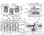
- FIG. 1 is a circuit diagram of an SRAM cell for explaining a columnar semiconductor memory device having an SGT according to a first embodiment of the present invention.
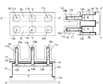
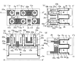
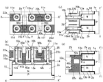
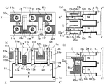
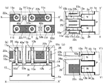
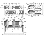
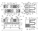
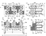
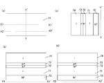
- FIGS. 7A and 7B are a plan view (a) and cross-sectional views (b) and (c), respectively, for explaining the method of manufacturing the columnar semiconductor memory device having the SGT according to the first embodiment.
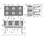
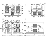
- FIGS. FIGS. 7A and 7B are a plan view (a) and cross-sectional views (b) and (c), respectively, for explaining the method of manufacturing the columnar semiconductor memory device having the SGT according to the first embodiment.
- FIGS. 7A and 7B are a plan view (a) and cross-sectional views (b) and (c), respectively, for explaining the method of manufacturing the columnar semiconductor memory device having the SGT according to the first embodiment.
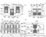
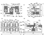
- FIGS. FIGS. 7A and 7B are a plan view (a) and cross-sectional views (b) and (c), respectively, for explaining the method of manufacturing the columnar semiconductor memory device having the SGT according to the first embodiment.
- FIGS. FIGS. 7A and 7B are a plan view (a) and cross-sectional views (b) and (c), respectively, for explaining the method of manufacturing the columnar semiconductor memory device having the SGT according to the first embodiment.
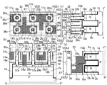
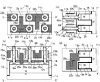
- FIGS. It is the top view (a) for demonstrating the manufacturing method of the columnar semiconductor memory device which has SGT which concerns on 1st Embodiment, and a cross-section figure (b), (c), (d). It is the top view (a) for demonstrating the manufacturing method of the columnar semiconductor memory device which has SGT which concerns on 1st Embodiment, and a cross-section figure (b), (c), (d).
- FIGS. 1-10 It is the top view (a) for demonstrating the manufacturing method of the columnar semiconductor memory device which has SGT which concerns on 1st Embodiment, and a cross-section figure (b), (c), (d). It is the top view (a) for demonstrating the manufacturing method of the columnar semiconductor memory device which has SGT which concerns on 1st Embodiment, and a cross-section figure (b), (c), (d). It is the top view (a) for demonstrating the manufacturing method of the columnar semiconductor memory device which has SGT which concerns on 1st Embodiment, and a cross-section figure (b), (c), (d).
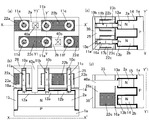
- 7A and 7B are a plan view (a) and cross-sectional views (b), (c), and (d), respectively, for explaining a method of manufacturing a pillar-shaped semiconductor memory device having an SGT according to a second embodiment of the present invention. It is the top view (a) for demonstrating the manufacturing method of the columnar semiconductor memory device which has SGT which concerns on 2nd Embodiment, and a cross-section figure (b), (c), (d). It is the top view (a) for demonstrating the manufacturing method of the columnar semiconductor memory device which has SGT which concerns on 2nd Embodiment, and a cross-section figure (b), (c), (d).
- FIGS. 7A and 7B are a plan view (a) and cross-sectional views (b), (c), and (d), respectively, for explaining a method of manufacturing a pillar-shaped semiconductor memory device having an SGT according to a second embodiment of the present invention.
- FIGS. 7A and 7B are a plan view (a) and cross-sectional views (b), (c), and (d), respectively, for explaining a method of manufacturing a pillar-shaped semiconductor memory device having an SGT according to a second embodiment of the present invention. It is the top view (a) for demonstrating the manufacturing method of the columnar semiconductor memory device which has SGT which concerns on 2nd Embodiment, and a cross-section figure (b), (c), (d).
- FIGS. 7A and 7B are a plan view (a) and cross-sectional views (b), (c), and (d), respectively, for explaining a method of manufacturing a pillar-shaped semiconductor memory device having an SGT according to a second embodiment of the present invention. It is the top view (a) for demonstrating the manufacturing method of the columnar semiconductor memory device which has SGT which concerns on 2nd Embodiment, and a cross-section figure (b), (c), (d).
- FIGS. 7A and 7B are a plan view (a) and cross-sectional views (b), (c), and (d), respectively, for explaining a method of manufacturing a pillar-shaped semiconductor memory device having an SGT according to a second embodiment of the present invention. It is the top view (a) for demonstrating the manufacturing method of the columnar semiconductor memory device which has SGT which concerns on 2nd Embodiment, and a cross-section figure (b), (c), (d).
- FIGS. 7A and 7B are a plan view (a) and cross-sectional views (b), (c), and (d), respectively, for explaining a method of manufacturing a pillar-shaped semiconductor memory device having an SGT according to a second embodiment of the present invention.
- FIGS. 7A and 7B are a plan view (a) and cross-sectional views (b), (c), and (d), respectively, for explaining a method of manufacturing a pillar-shaped semiconductor memory device having an SGT according to a second embodiment of the present invention. It is the top view (a) for demonstrating the manufacturing method of the columnar semiconductor memory device which has SGT which concerns on 2nd Embodiment, and a cross-section figure (b), (c), (d).
- top view (a) for demonstrating the manufacturing method of the inverter chain circuit apparatus which has SGT which concerns on 1st Embodiment, and a cross-section figure (b), (c), (d). It is the top view (a) for demonstrating the manufacturing method of the inverter chain circuit apparatus which has SGT which concerns on 1st Embodiment, and a cross-section figure (b), (c), (d). It is the top view (a) for demonstrating the manufacturing method of the inverter chain circuit apparatus which has SGT which concerns on 1st Embodiment, and a cross-section figure (b), (c), (d).
- FIG. 1 shows an equivalent circuit diagram of the SRAM cell structure of this embodiment.
- the SRAM cell circuit includes two inverter circuits.
- One inverter circuit is composed of a P-channel SGT_Pc1 as a load transistor and an N-channel SGT_Nc1 as a drive transistor.
- Another inverter circuit is composed of P-channel SGT_Pc2 as a load transistor and N-channel SGT_Nc2 as a drive transistor.
- the gate of P-channel SGT_Pc1 and the gate of N-channel SGT_Nc1 are connected.
- the drain of P-channel SGT_Pc2 is connected to the drain of N-channel SGT_Nc2.
- the gate of P channel SGT_Pc2 and the gate of N channel SGT_Nc2 are connected.
- the drain of the P-channel SGT_Pc1 is connected to the drain of the N-channel SGT_Nc1.
- the sources of the P-channels SGT_Pc1 and Pc2 are connected to the power supply terminal Vdd.
- the sources of the N-channel SGT_Nc1 and Nc2 are connected to the ground terminal Vss.
- the selected N-channels SGT_SN1 and SN2 are disposed on both sides of the two inverter circuits.
- the gates of the selected N-channels SGT_SN1 and SN2 are connected to the word line terminal WLt.
- the source and drain of the selected N-channel SGT_SN1 are connected to the N-channel SGT_Nc1, the drain of the P-channel SGT_Pc1 and the bit line terminal BLt.
- the source and drain of the selected N-channel SGT_SN2 are connected to the N-channel SGT_Nc2, the drain of the P-channel SGT_Pc2 and the inverted bit line terminal BLRt.
- the circuit having the SRAM cell of the present embodiment (hereinafter referred to as "SRAM cell circuit") comprises two P-channels SGT_Pc1 and Pc2 and four N-channels SGT_Nc1, Nc2, SN1 and SN2 Total of six SGTs.
- an N layer 2 is formed on a P layer substrate 1 by an epitaxial growth method.
- N + layers 3 a and 3 b and a P + layer 4 are formed on the surface of the N layer 2 by, eg, ion implantation.
- the i layer 5 is formed on the N + layers 3 a and 3 b and the P + layer 4 by epitaxial growth.
- an insulating material layer 6 formed of a silicon oxide (SiO 2 ) layer (not shown), a silicon nitride (SiN) layer (not shown), and an SiO 2 layer (not shown) on the i layer 5
- the N layer 2 contains a larger donor impurity concentration than the acceptor impurity concentration contained in the P layer substrate 1.
- the N + layers 3a and 3b and the P + layer 4 serve as the source or drain of SGT, it is desirable that the N + layers 3a and 3b and the P + layer 4 contain donor or acceptor impurities as high as possible.
- the i-layer 5 may be an acceptor and a P layer or an N layer containing donor or acceptor impurities as well as intrinsic conductivity type not including donor impurities.
- the insulating material layers 6 a and 6 b are formed on the i layer 5 by the lithography method and the RIE (Reactive Ion Etching) method of the insulating material layer 6. Then, using the insulating material layers 6a and 6b as a mask, the i layer 5, N + layers 3a and 3b, P + layer 4, N layer 2 and P layer 1 are etched to form an i layer under the insulating material layer 6a.
- Si pillar stand consisting P layer substrate 1a, i layer 5b under the insulating material layer 6b, N + layer 3 cc (not shown), A Si pillar composed of 3dd (not shown), P + layer 4b, N layer 2b, and P layer substrate 1a is formed.
- the insulating material layer 6a is patterned using lithography and RIE to form insulating material layers 10a, 10b, 10c, 10d (not shown), 10e, 10f. Form. Then, using the insulating material layers 10a to 10f as masks, the insulating material layers 6a and 6b, the i layers 5a and 5b, and the N + layers 3aa, 3bb, 3cc, and 3dd are etched to form Si pillars 11a, 11b, 11c, and 11d. , 11e, 11f.
- N + layers 12a, 12b and 12c (not shown) and 12d (not shown) and P + layers 13a and 13b are formed at the bottom of the Si pillars 11a to 11f. Then, an N layer 2a is formed on the P layer substrate 1a under the N + layers 12a and 12b. Then, an N layer 2 b is formed on the P layer substrate 1 a under the N + layers 12 c and 12 d.
- the whole is covered with a SiN layer (not shown), and the position of the upper surface of the Si pillars 11a to 11f is N
- the SiO 2 layer 15 is formed above the upper surfaces of the + layers 12a, 12b, 12c, 12d and the P + layers 13a, 13b.
- the SiN layer surrounding the upper Si pillars 11a to 11f and the SiO 2 layer are removed.
- a thin SiO 2 layer (not shown) is formed on the side surfaces of the Si pillars 11a to 11f by, for example, chemical cleaning, a hafnium oxide (HfO 2 ) layer 16 which is a gate insulating material layer is formed on the whole. , ALD (Atomic Layer Deposition) method to form. Then, a titanium nitride (TiN) layer 17 which is a gate conductor layer is formed on the whole.
- a tungsten (W) film (not shown) is formed so that the upper surface position thereof is above the insulating material layers 10a to 10f. Then, CMP by (Chemical Mechanical Polish) method, W layer and, by polishing the TiN layer 17, W layer 20 on the surface position is like the surface position on the insulating material layer 10a ⁇ 10f and the TiN layer 17a, HfO 2 The layer 16a is formed.
- the W layer 20 and the TiN layer 17a are etched back (etch back) using the RIE (Reactive Ion Etching) method to form the W layer 20a and the TiN layer 17b.
- RIE Reactive Ion Etching
- the upper surface position of the SiO 2 layer is made the same as the upper surface position of the insulating layers 10a to 10f by CMP.
- the SiO 2 layer 25 is formed by polishing.
- the SiN layer 26 is formed on the whole.
- the SiN layer 26 and the SiO 2 layer 25 are etched using the lithography method and the RIE method, and the bottom part becomes the upper surface of the W layers 22a to 22d.
- the N + layer 12a and the P + layer 13a In plan view, the N + layer 12a and the P + layer 13a.
- the SiO 2 layer 25 empty hole 27a, the bottom of 27b, due overetching of the SiO 2 layer 25, becomes lower than the upper surface of the W layer 22a ⁇ 22 d.
- the etching of the W layers 22a to 22d is further advanced.
- the etching of the SiO 2 layer 25 is further advanced.
- the bottom is below the upper surface of W layer 22c, and in plan view, on the boundary between N + layer 12a and P + layer 13a, and the bottom is on N + layer 12a, P + layer 13a.
- a contact hole 27aa formed so as to be at the surface position or inside the N + layer 12a and the P + layer 13a is formed.
- the bottom is below the upper surface of W layer 22b, and on a boundary between N + layer 12d and P + layer 13b in plan view, and the bottom is N + layer 12d, P + layer 13b.
- a contact hole 27aa formed so as to be at the upper surface position, or inside the N + layer 12d and the P + layer 13b is formed.
- a barrier conductor layer made of, for example, Ti and TiN is formed in the contact holes 27aa and 27bb by using the ALD method.
- a W layer (not shown) is formed on the entire surface so that the upper surface position thereof is higher than the upper surface positions of the insulating material layers 10a to 10f and the SiO 2 layer 25.
- the W layer and the barrier conductor layer on the SiO 2 layer 25 are polished and removed by the CMP method.
- the upper portions of the W layer and the barrier conductor layer in the contact holes 27aa and 27bb are etched to form barrier conductor layers 28a and 28b and W layers 29a and 29b.
- the N + layer 12a, the P + layer 13a, and the W layer 22c are connected via the barrier conductor layer 28a and the W layer 29a.
- the N + layer 12 d, the P + layer 13 b, and the W layer 22 b are connected via the barrier conductor layer 28 b and the W layer 29 b.
- an SiO 2 layer (not shown) is formed on the entire surface, and the upper surface position thereof is formed higher than the upper surface positions of the insulating material layers 10a to 10f.
- the SiO 2 layer is polished by the CMP method so that the upper surface position is the same as the upper surface position of the insulating material layers 10a to 10f, and the barrier conductor layers 28a, 28b, W in the contact holes 27aa, 27bb.
- the SiO 2 layers 30a, 30b are formed on the layers 29a, 29b.
- the upper layer of the SiO 2 layers 25, 30a, and 30b is etched by the RIE method.
- an SiO 2 layer 32 is formed on the outer periphery of the Si pillars 11a to 11f.
- N + layers 33a, 33c, 33d (not shown), 33f (not shown), and Si pillars 11b, 11e are formed on top of the Si pillars 11a, 11c, 11d, 11f by lithography and ion implantation. Form P + layers 33b, 33e on top.
- the N + layers 33a, 33c, 33d, and 33f and the P + layers 33b and 33e become the source or drain of SGT, it is desirable that the N + layers 33a, 33c, 33d, and 33f contain as many donor or acceptor impurities as possible.
- a SiO 2 layer 35 is formed on the whole.
- the contact holes 36a and 36d are formed on the W layers 22a and 22d, and the contact holes 36b and 36d are formed on the Si pillars 11c and 11d by the lithography method and the RIE etching method.
- the word wiring metal layer WL connected to the W layers 22a and 22d via the contact holes 36a and 36b, and the N + layers 33c and 33d via the contact holes 36b and 36c.
- the ground wiring metal layers Vss1 and Vss2 are formed.
- the SiO 2 layer 37 is formed on the whole.
- contact holes 38a, 38b, 38c and 38d are formed on the Si pillars 11a, 11b, 11e and 11f by using the lithography method and the RIE etching method. Then, on the SiO 2 layer 37, the bit wiring metal layer BL connected to the N + layer 33a via the contact hole 38a, and the power supply wiring metal connected to the P + layers 33b and 33e via the contact holes 38b and 38c. A layer VDD and an inversion bit line metal layer RBL connected to the N + layer 33 f via the contact hole 38 d are formed. Thereby, the SRAM cell circuit is formed on the P layer substrate 1a.
- the N + layer 12a, the P + layer 13a, and the W layer 22c connected to the gate TiN layer 17b are connected via the W layer 29a.
- W layer 29a has a structure embedded in contact hole 27aa in W layer 22c.
- the W layer 29b is embedded in the contact hole 27bb.
- the W layer 22c and the W layer 29a are connected more securely than in the case where the embedding is not performed.
- the connection area of the W layer 22c and the W layer 29a can be increased, the connection resistance between the W layer 22c and the W layer 29a can be reduced as compared with the case without this embedding.
- the upper surface position of the W layer 29a, 29b is the upper surface position of the gate TiN layer 23a, 23b, 23c, 23d and the W layer 22a, 22b, 22c connected to the gate TiN layer 23a, 23b, 23c, 23d. , 22d and the lower surface position.
- the upper surface position of W layers 29a and 29b can be reliably made lower than the upper surface positions of gate TiN layers 23a, 23b, 23c and 23d and W layers 22a, 22b, 22c and 22d.
- the bottom of contact hole 27aa is below the upper surface of W layer 22c, and in plan view on the boundary between N + layer 12a and P + layer 13a, and the bottom thereof is N + layer 12a. , The upper surface position of the P + layer 13a, or the inside of the N + layer 12a and the P + layer 13a.
- the bottom of the contact hole 27aa is N + layer 12a, by forming such that the inside of the P + layer 13a, can be widely and W layer 29a, the N + layer 12a, the contact area between the P + layer 13a . Thereby, the connection resistance between the W layer 29a, the N + layer 12a, and the P + layer 13a can be reduced.
- the connection resistance reduction effect increases as the area of the contact hole 27aa in a plan view decreases. This is effective for high integration of the SGT circuit.
- contact holes 40a and 40b are formed on the region including the boundary of N + layer 12a and P + layer 13a and on the region including the boundary of N + layer 12d and P + layer 13b.
- barrier conductor layers 41a and 41b (not shown) in contact holes 40a and 40b so that the upper surface position thereof is lower than the upper surface position of W layers 22a to 22d.
- W layers 42a and 42b (not shown).
- SiO 2 layers 43a and 43b are formed on the W layers 42a and 42b and the barrier conductor layers 41a and 41b and in the contact holes 40a and 40b.
- the contact hole 40a, the contact hole 46a connected to the W layer 22c, the contact hole 40b, and the contact connected to the W layer 22b The holes 46 b are formed by the lithography method and the RIE etching method of the SiN layer 45 and the SiO 2 layer 25.
- the bottom of contact hole 46a is the upper surface of W layers 42a and 22c
- the bottom of contact hole 46b is the upper surface of W layers 42b and 22b.
- the W layers 42a, 42b, 22c, 22b and the barrier conductor layers 41a, 41b are subsequently etched.
- contact holes 46aa and 46bb having depressions connecting the upper surfaces of W layers 22c and 22b to the inside are formed.
- a barrier conductor layer (not shown) and a W layer (not shown) are formed in the contact holes 46aa and 46bb and on the SiN layer 45, and the barrier conductor layer and W are formed by CMP.
- the layer is polished to the top surface of the SiO 2 layer 25.
- the barrier conductor layer and the W layer are etched by the RIE method.
- the barrier conductor layers 48a and 48b and the W layers 49a and 49b are lower in upper surface position than the upper surface position of the gate W layers 22a to 22d. And.
- SiO 2 layers 50a and 50b are formed in the contact holes 46aa and 46bb on the barrier conductor layers 48a and 48b and the W layers 49a and 49b. Then, by performing the same steps as in FIGS. 2I to 2K, an SRAM circuit is formed on P layer substrate 1a.
- the connection between the N + layer 12a, the P + layer 13a and the W layer 22c, and the connection between the N + layer 12d and the P + layer 13b and the W layer 22b are performed by a single lithography method and RIE etching Method via contact holes 27aa and 27bb (see FIG. 2H).
- the first contact holes 40a and 40b are formed on the top surfaces of the N + layers 12a and 12d and the P + layers 13a and 13b
- the second contact holes 46aa and 46bb are The inside of the first contact holes 40a and 40b was formed after the upper surface position was embedded with W to the upper surface position of the W layers 22a to 22d. Therefore, the second contact holes 46aa and 46bb can be formed on the W layers 42a and 42b and the W layers 22b and 22c to the same depth. Thus, the W layers 49a and 49b can be reliably formed.
- the steps up to the step shown in FIG. 3D of the second embodiment are performed, and are on the barrier conductor layers 41a and 41b and the W layers 42a and 42b and at the bottoms of the contact holes 46aa and 46bb.
- W layers 51a and 51b are formed using a W selective epitaxial method.
- W atoms do not adhere to the surfaces of the SiO 2 layer 25 as the insulating material layer and the insulating material layers 10a to 10f, and W on the bottom of the contact hole 46aa It is formed on the layers 42a and 22c, on the barrier conductor layer 41a, on the W layers 42b and 22b at the bottom of the contact hole 46bb, and on the barrier conductor layer 41b. Then, by further advancing the growth of W and performing the horizontal growth of W, the W layer 51a connected to the W layer 42a and the W layer 22c, and the W connected to the W layer 22b and the W layer 42b The layer 51 b is formed.
- the upper surface of the W layers 51a and 51b is located on the SiO 2 layer 25 and the insulating material layers 10a to 10f.
- SiO 2 layers 52a and 52b which are the same as the upper surface position are formed in the contact holes 46aa and 46bb. Then, by performing the steps shown in FIGS. 2J and 2K of the first embodiment, an SRAM circuit can be formed on the P layer substrate 1a.
- the barrier conductor layer (not shown) and the W layer (not shown) are formed in the contact holes 46aa and 46bb and on the SiN layer 45.
- the barrier conductor layer and the W layer are polished to the upper surface of the SiO 2 layer 25 by the CMP method.
- the barrier conductor layer and the W layer are etched by the RIE method.
- barrier conductor layers 48a and 48b and W layers 49a and 49b are formed at the bottoms of the contact holes 46aa and 46bb on the barrier conductor layers 48a and 48b and the W layers 49a and 49b.
- the W layer 51a, 41a, 41b and the W layer 42a, 42b are directly formed by the direct W selective growth method without using the CMP method and the RIE method. 51b was formed. This simplifies the manufacturing process.
- the process of forming the contact holes 40a and 40b in FIG. 3A is performed, and thereafter, the entire SiO 2 layer (not shown) is formed by CVD (Chemical Vapor Deposition) method or ALD method. Then, the SiO 2 layer is deposited by RIE and etched to form SiO 2 layers 53 a and 53 b on the side surfaces of the contact holes 40 a and 40 b .
- barrier material layers 54a and 54b and W layers 55a and 55b are formed in the contact holes 40a and 40b. Then, the SRAM circuit can be formed on the P layer substrate 1a by performing the same process as the second embodiment.
- the SiO 2 layers 53a and 53b which are insulating material layers, exist between the W layers 55a and 55b and the W layers 22a to 22d. As a result, it is possible to prevent a short circuit failure between the W layers 55a and 55b and the W layers 22a to 22d caused by the mask misalignment in the lithography method when forming the contact holes 40a and 40b.
- a SiN layer 56 is entirely formed by the ALD method.
- contact holes 27aa and 27bb are formed on the N + layers 12a and 12d, the P + layers 13a and 13b, and the W layers 22c and 22b by lithography and RIE. Then, by performing the steps shown in FIGS. 2I to 2K, an SRAM circuit can be formed on the P layer substrate 1a.
- the SiN layer 56 and the SiO 2 layer 25 are provided between the contact holes 27aa and 27bb and the W layers 22a to 22d.
- the contact holes 27aa and 27bb are formed by etching the SiO 2 layer 25 by the RIE method.
- the SiN layer 56 acts as an etching stopper for the etching of the SiO 2 layer 25.
- a low dielectric constant material whose upper surface position also becomes the surface position of the W layer 22a ⁇ 22 d, for example, carbon-containing SiO 2 (SiOC: Carbon-incorporated Silicon Oxide) layer 60 is formed.
- the SiOC layer 60 is deposited by depositing a SiOC layer (not shown) on the entire surface so that the upper surface position is above the upper surface of the insulating material layers 10a to 10f, and the upper surface is made flat by the CMP method. After that, etching is performed by RIE etching so that the upper surface position becomes the upper surface position of the W layers 22a to 22d.
- the SiO 2 layer 61 is formed to surround the outer periphery of the Si pillar.
- the SiN layer 26 is formed on the whole.
- the bottom is below the upper surface of W layer 22c, and contact holes 27aa on N + layer 12a and P + layer 13a, and the bottom is below the upper surface of W layer 22b.
- contact holes 27bb on the N + layer 12d and the P + layer 13b can be formed on the P layer substrate 1a.
- a SiOC layer 60 (dielectric constant: 2.7 to 2) having a low dielectric constant is used. 9) is used.
- the coupling capacitances between the W layers 22a to 22d which are gate conductor layers on both sides of the low dielectric constant SiOC layer 60 and the W layers 29a and 29b which are connection wiring conductor layers are It can be made smaller than the embodiment.
- power consumption can be reduced by reducing the driving voltage.
- the SiO 2 layers 25, 30a and 30b are removed as shown in FIG. 8A.
- a space 63 including a narrow portion is formed between the W layers 22a to 22d and the W layer 29a.
- the SiO 2 layer 64 is formed by the CVD method.
- holes 65a, 65b, 65c and 65d are formed in narrow portions between the W layers 22a to 22d and the W layers 29a and 29b.
- an SRAM circuit is formed on the P layer substrate 1a by performing the same steps as in FIGS. 2J and 2K in the first embodiment.
- the holes 65a, 65b, and 65c having a non-dielectric constant of 1 exist between the W layers 22a to 22d, which are gate conductor layers, and the W layers 29a and 29b, which are connection wiring conductor layers.
- the coupling capacitance between the W layers 22a to 22d, which are gate conductor layers, and the W layers 29a and 29b, which are connection wiring conductor layers is a SiO 2 layer having a non-dielectric constant of 3.9 to 4.3 as a whole
- the second embodiment can be made smaller than the first embodiment using 25. Thus, power consumption can be reduced by reducing the driving voltage.
- the i layer 71, the N + layer 72, the P + layer 73, and the i layer 74 are formed on the N + layer substrate 70 sequentially from the bottom by using the Si epitaxial growth method.
- mask material layers 75a, 75b, and 75c made of, for example, an SiO 2 layer and an SiN layer are formed.
- Si pillars 76a, 76b and 76c are formed using the mask material layer as an etching mask.
- N + layers 72a, 72b, 72c and P + layers 73a, 73b, 73c are formed in the Si pillars 76a, 76b, 76c.
- the Si pillars 76a, 76b and 76c are surrounded to form, for example, a HfO2 layer (not shown) which is a gate insulating material layer.
- a gate conductor layer for example, a TiN layer (not shown) and a W layer (not shown) are formed.
- the SiN layer 90a whose upper surface position is located at the lower end of the N + layers 72a, 72b and 72c is formed in the outer peripheral portion of the W layer.
- the W layer, the TiN layer, and the HfO 2 layers 79a, 79b, 79c are horizontal with the lower end being the lower end of the N + layers 72a, 72b, 72c and the upper end being the upper end of the P + layers 73a, 73b, 73c.
- the HfO2 layer, the TiN layer, and the W layer are vertically separated, and the HfO2 layers 78, 79a, 79b, 79c, the TiN layers 80a, 80b, 80c, 81a, 81b, 81c, the W layers 82a, 82b, 82c, 83a. , 83b, 83c are formed.
- the layers 80b and 81b and the W layers 82b and 83b are arranged in the up-down direction differently.
- SiO 2 layers 85 a, 85 b, 85 c, 86 a, 86 b and 86 c are formed on the upper and lower side surfaces of the holes.
- NiSi layer 88a connected to the side surfaces of N + layer 72a and P + layer 73a
- NiSi layer 88b connected to the side surfaces of N + layer 72b and P + layer 73b
- the NiSi layers 88a, 88b, 88c, the TiN layers 80a, 80b, 80c, 81a, 81b, 81c, the W layers 82a, 82b, 82c, 83a, 83b, 83c are Si pillars 76a, 76b, 76c.
- a contact hole 93a which penetrates the SiO 2 layer 90c, the W layer 83a, the SiO 2 layer 86a, the SiO 2 layer 90b, and the SiO 2 layer 85a and the bottom thereof reaches the inside of the W layer 82a.
- a contact hole 93b which penetrates the SiO 2 layer 90c, the W layer 83b, the SiO 2 layer 86b, the SiO 2 layer 90b, and the SiO 2 layer 85b and the bottom thereof reaches the inside of the W layer 82b;
- a contact hole 93a is formed which penetrates 83c, the SiO 2 layer 86c, the SiO 2 layer 90b, and the SiO 2 layer 85c and the bottom thereof reaches the inside of the W layer 82c.
- the barrier conductor layers 91a, 91b, 91c whose upper surface position is lower than the upper surface position of the W layers 83a, 83b, 83c, W layers 92a, 92b, 92c, Form
- a contact hole 97a which penetrates the SiO 2 layer 90c and the SiO 2 layer 90b and whose bottom is connected to the top of the NiSi layer 88a and the inside of the W layer 83b, and the bottom is on the NiSi layer 88b.
- a contact hole 97c connected to the inside of the W layer 83c, and a contact hole 97c connected to the bottom of the NiSi layer 88c and the inside of the W layer (not shown).
- barrier conductor layers 95a, 95b, 95c whose upper surface positions are lower than the upper surface positions of W layers 83a, 83b, 83c, and W layers 96a, 96b, 96c inside contact holes 97a, 97b, 97c, Form
- the upper portions of the TiN layers 81a, 81b, 81c, the HfO 2 layers 79a, 79b, 79c, the SiO layer 90c, and the mask material layers 75a, 75b, 75c are removed by RIE.
- a P + layer 98a is formed on the top of the Si pillar 76a, a P + layer 98b on the top of the Si pillar 76b, and a P + layer 98c on the top of the Si pillar 76c by ion implantation, for example.
- contact holes 97a, 97b, 97c are filled, and a SiO 2 layer 99 having a flat upper surface is formed on the whole.
- the contact hole 100a is formed on the W layer 92a, and the contact holes 100b, 100c, and 100d are formed on the P + layers 98a, 98b, and 98c.
- an input wiring metal layer VIN connected to W layers 82a and 83a through contact hole 100a, and a power supply wiring metal layer Vdd connected to P + layers 98a, 98b and 98c through contact holes 100b, 100c and 100d,
- the bottom N + layer substrate 70 a is connected to the ground wiring metal layer (not shown) outside.
- a CMOS inverter chain circuit is formed on the N + layer substrate 70a.
- the NiSi layer 88a formed in three layers in the vertical direction and the gate conductor layer A certain W layer 82 b and W layer 83 b are connected via W layers 96 a and 92 b which are connection conductor layers.
- the N + layer 12a and the P + layer 13a correspond to the NiSi layer 88a
- the W layer 22c of the gate corresponds to the W layer 83b of the gate
- the W layer 42a which is a connection conductor layer is connected.
- the W layer 49a which is a connection conductor layer corresponds to the W layer 92a of the conductor layer, and corresponds to the W layer 96a of the connection conductor layer.
- the bottom portion of the W layer 42a, which is the connection conductor layer rests inside the W layer 22c of the gate, while in the present embodiment, the W layer 92a, which is the connection conductor layer, is The W layer 82b of the gate and the W layer 83b of the gate are formed to be connected in the vertical direction. This indicates that connections can be formed at high density between the overlapping layers in plan view. Thereby, the density of the circuit using SGT can be increased.
- the SRAM circuit is formed on the P layer substrate 1a.
- another substrate such as SOI (Silicon On Insulator) may be used. The same applies to the other embodiments.
- the W layer 29 a connects the N + layer 12 a at the bottom of one Si pillar 11 a and the gate W layer 22 c of another Si pillar 11 d. Further, the N + layer 12a at the bottom of one Si pillar 11a and the gate W layer 22c of another Si pillar 11e are connected by the W layer 29a. Similarly, the P + layer 13a at the bottom of one Si pillar 11b and the gate W layer 22c of the other Si pillars 11d and 11e are connected by the W layer 29a.
- the present invention is applied to the connection between the impurity layer at the bottom of the Si pillar in which one SGT is formed and the gate conductor layer of the Si pillar in which another SGT is formed. Therefore, according to the present invention, a circuit connecting the source or drain of one MOS field effect transistor to the gate of another MOS field effect transistor, such as various flip flop circuits, latch circuits, sense circuits of DRAM (Random Access Memory) It can be applied to Thereby, high integration of these circuits can be achieved. The same applies to the other embodiments.
- the gate TiN layers 23a to 23d and the W layers 22a to 22d are formed in connection with the gate TiN layers 23a to 23d.
- the gate TiN layers 23a-23d and the W layers 22a-22d may be other material layers.
- the gate TiN layers 23a-23d and the W layers 22a-22d may be formed of the same material layer.
- the gate TiN layers 23a to 23d and the W layers 22a to 22d, including the barrier metal layer may be conductor layers composed of a plurality of layers. The same applies to the other embodiments.
- the N + layers 12a to 12d and the P + layers 13a and 13b at the bottom of the Si pillars 11a to 11f are formed extending in the horizontal direction while being connected to the bottoms of the Si pillars 11a to 11f.
- the horizontally extending region serves as an impurity region connection layer for forming the connection W layers 29a and 29b on this region.
- the horizontally extending impurity region connection layer may be formed of another semiconductor or conductor material layer. The same applies to the other embodiments.
- the W layers 22a to 22d extend in the horizontal direction so as to be connected to the TiN layers 23a to 23d which are the gate conductor layers.
- the W layers 22a to 22d have a role of gate connection conductor layers for forming the connection W layers 29a and 29b on the W layers 22a to 22d.
- the horizontally extending gate connection conductor layer may be the same conductor material layer as the gate conductor layer or a different conductor material layer. The same applies to the other embodiments.
- the contact holes 27aa and 27bb are formed on the N + layers 12a and 22d and the P + layers 13a and 13b.
- the contact holes 27aa and 27bb may be formed on the silicide layer or metal layer formed on the N + layers 12a and 22d and the P + layers 13a and 13b.
- an N + layer or a P + layer is formed under the Si pillars 11a to 11f, and contact holes 27aa and 27bb are formed on the low resistance semiconductor layer or conductor layer connected to the side of the N + layer or P + layer. It may be done.
- the low resistance semiconductor layer connected to the side surface of the N + layer or the P + layer may be formed by connecting the same semiconductor layers, or may be formed of different semiconductor layers. The same applies to the other embodiments.
- the HfO 2 layer 16a is used as the gate insulating film, but another material layer may be used.
- the gate insulating material layer may be formed of a plurality of material layers. The same applies to the other embodiments.
- the Si pillars 11a to 11f and the N + layers 12a to 12d, 33a, 33c, 33d, and 33f, and the P + layers 13a, 13b, 33b, and 33e made of Si are used.
- Semiconductor materials may be used. The same applies to the other embodiments.
- the source and drain of the SGT are formed of the same conductivity.
- tunnel type SGTs having different conductivity of the source and drain may be used. The same applies to the other embodiments.
- patterning of each material layer is performed using a lithography method.
- a lithography method not only patterning of the resist layer, but also a single layer or plural layers of material may be formed under the resist layer to form a mask material layer of the material layer to be etched. The same applies to the other embodiments.
- the contact holes 43a on the N + layer 12a and the P + layer 13a, and the contact holes 43b on the N + layer 12d and the P + layer 13b are formed.
- the contact hole 46a straddling the contact hole 43a and the W layer 22c, the contact hole 43b and the contact hole 46b spanning the W layer 22b are formed.
- the order of forming the contact holes 43a and 43b and the contact holes 46a and 46b may be changed.
- the barrier conductor layers 48a and 48b are formed on the W layers 42a and 22b, but the barrier conductor layers 48a and 48b are not present in connection between the W layers 42a and 22b and the W layers 49a and 49b. May be When the W layer 42a, 22b and the W layer 49a, 49b are replaced with another conductive material layer, the barrier conductive layer may be omitted if the barrier conductive layer may not be necessary for circuit operation. . The same applies to other embodiments in which at least two conductor layers are connected, such as the connection between the W layers 42a and 22b and the W layers 49a and 49b.
- the W layers 51a, 51b, 55a, 55b are formed by the selective growth method.
- other conductor materials by selective growth may be used.
- the SiO 2 layers 53a and 53b are formed on the side surfaces of the contact holes 40a and 40b, but instead of the SiO 2 layers 53a and 53b, another insulating material layer may be used.
- the SiN layer 56 in the fifth embodiment may be another insulating material layer as long as it is a material that becomes an etching stopper with respect to etching when forming the contact holes 27aa and 27bb.
- the SiOC layer 60 which is a low dielectric constant material is used, but another material layer such as porous silica or SiOF may be used.
- SiO 2 layer 64 instead of the SiO 2 layer 64 in the seventh embodiment, another insulating layer may be used.
- the holes 65a and 65b are formed in the SiO 2 layer 64 between the W layers 22a and 22b on both sides of the W layer 29a.
- the formation locations of these holes 65a to 65d may differ depending on the design of the SRAM cell or other circuits.
- the gate W layer 82b and the gate W layer 83b are connected by the W layer 92b which is a connection conductor layer, but the W layer 83b and the impurity in the same Si pillar 76b are formed by the forming circuit. It may be a connection with either or both of the region P + layer 73 b and the N + layer 72 b or a connection with the impurity region N + layer 70 a.
- the W layer 96a connects the NiSi layer 88a connected to the P + layer 73a and the N + layer 72a, and the W layer 83b connected to the gate TiN layer 81b.
- the W layer 96a may be connected to the connection conductor layer connected to either the P + layer 73a or the N + layer 72a depending on the circuit to be formed.
- the W layer 96a may be connected to one or both of the W layer 82a and the N + layer 70a below the P + layer 73a and the N + layer 72a. This is the same in relation to the Si pillars 76c other than the Si pillars 76a. Further, depending on the circuit to be formed, the same is true for the connection spanning between the Si pillar 76 b and a plurality of other Si pillars.
- the present invention is applied to a circuit in which two SGTs are formed in one Si column, but one or three or more SGTs are formed in one Si column.
- the invention applies.
- a circuit in which one SGT is formed in one Si column it has a gate conductor layer and a conductor layer connected via a contact hole penetrating the impurity region of the source or the drain below the gate conductor layer.
- through contact holes are formed corresponding to the contact holes 93b, for example, connecting three or more conductor layers or impurity regions.
- the lower end is the lower end of the N + layers 72a, 72b and 72c
- the upper end is the upper end of the P + layers 73a, 73b and 73c.
- the HfO2 layer, the TiN layer, and the W layer are vertically separated, and the HfO2 layers 78, 79a, 79b, 79c, the TiN layers 80a, 80b, 80c, 81a, 81b, 81c, the W layers 82a, 82b, 82c, 83a. , 83b, 83c were formed.
- the HfO 2 layer 78, the TiN layers 80a, 80b, 80c, the W layers 82a, 82b, 82c are formed, and the SiO 2 layers 85a, 85b, 85c, 86a, 86b, 86c are formed on the upper and lower sides.
- the NiSi layers 88a, 88b and 88c may be formed, and the HfO 2 layers 79a, 79b and 79c, the TiN layers 81a, 81b and 81c, and the W layers 83a, 83b and 83c may be formed.
- a conductor connection layer connected to the gate insulating layer, gate conductor layer, N + layers 72a, 72b, 72c, and P + layers 73a, 73b, 73c of each SGT by another method and material layer, the conductor connection layer Upper and lower insulating layers may be formed.
- the bottom of the contact hole 27aa is formed inside the N + layer 12a and the P + layer 13a, whereby the W layer 29a and the N + layer 12a and the P + layer 13a are formed. It was stated that the contact area could be increased. Thereby, the connection resistance between the W layer 29a, the N + layer 12a, and the P + layer 13a can be reduced. The same applies to the other embodiments.
- the present invention is capable of various embodiments and modifications without departing from the broad spirit and scope of the present invention.
- the embodiment described above is for describing an example of the present invention, and does not limit the scope of the present invention.
- the above-mentioned embodiment and modification can be combined arbitrarily. Furthermore, even if part of the configuration requirements of the above-described embodiment is removed as necessary, it is within the scope of the technical idea of the present invention.
Landscapes
- Semiconductor Memories (AREA)
- Metal-Oxide And Bipolar Metal-Oxide Semiconductor Integrated Circuits (AREA)
- Insulated Gate Type Field-Effect Transistor (AREA)
- Thin Film Transistor (AREA)
Abstract
Description
基板上に、垂直方向に配置される第1の半導体柱と、
前記第1の半導体柱の下方にある第1の不純物領域と、
前記第1の不純物領域に繋がり、且つ水平方向に延びている、半導体または導体よりなる第1不純物領域接続層と、
前記第1の半導体柱の上方にある第2の不純物領域と、
前記第1の不純物領域と、前記第2の不純物領域の間にある前記第1の半導体柱を囲んだ第1のゲート絶縁層と、
前記第1の絶縁層を囲んだ第1のゲート導体層と、
前記基板上に、垂直方向に配置される第2の半導体柱と、
前記第2の半導体柱の下方にある第3の不純物領域と、
前記第2の半導体柱の上方にある第4の不純物領域と、
前記第3の不純物領域と、前記第4の不純物領域の間にある前記第2の半導体柱を囲んだ第2のゲート絶縁層と、
前記ゲート絶縁層を囲んだ第2のゲート導体層と、
前記第2のゲート導体層に繋がり、且つ水平方向に延びている導体よりなる第2ゲート接続導体層と、
前記第1不純物領域接続層と、前記第2ゲート接続導体層と、に繋がり、且つ、平面視において、少なくとも前記第2ゲート接続導体層に重なる部分の底部の垂直方向での位置が、前記第2のゲート導体層と、前記第2ゲート接続導体層と、の上表面位置より低い第1のコンタクトホールと、
前記第1のコンタクトホール内に前記第1の不純物領域と、前記第2ゲート接続導体層と、に繋がる第1の接続導体層を有する、
ことを特徴とする。
ことが望ましい。
前記柱状半導体装置において、前記第2のゲート導体層と、前記第2ゲート接続導体層と、が同じ材料層よりなる、
ことが望ましい。
前記第1不純物領域接続層上または前記第2ゲート接続導体層上にある第2のコンタクトホールと、
前記第2のコンタクトホールが前記第1不純物領域接続層上にある場合は、前記第2ゲート接続導体層とに繋がり、前記第2のコンタクトホールが前記第2ゲート接続導体層上にある場合は、前記第1不純物領域接続層に繋がる、第3のコンタクトホールと、よりなり、
前記第3のコンタクトホールの底部が、前記第2のゲート導体層、及び前記第2ゲート接続導体層の上表面位置より下にあり、
前記第1の接続導体層が、前記第2のコンタクトホール内にある第2の接続導体層と、前記第2の接続導体層に繋がり、且つ前記第3のコンタクトホール内にある第3の接続導体層と、よりなる、
ことが望ましい。
前記第1ゲート接続導体層と、前記第2ゲート接続導体層との側面を囲んだ第1の層間絶縁層と、
前記第1の層間絶縁層側面を囲んだ、前記第1の層間絶縁層と異なる材料であり、且つ前記第1のコンタクトホール形成のための第2の層間絶縁層とを有する、
ことが望ましい。
ことが望ましい。
ことが望ましい。
前記第4のコンタクトホール内に、第4の接続導体層を有する、
ことが望ましい。
第1の不純物領域、第1の半導体柱及び第2の不純物領域が、基板上に垂直方向に階層的に配置されると共に、第3の不純物領域、第2の半導体柱及び第4の不純物領域が、基板上に垂直方向に階層的に配置されており、
前記第1の不純物領域は、前記第1の半導体柱の下方に配置されており、
前記第3の不純物領域は、前記第2の半導体柱の下方に配置されており、
半導体または導体の第1不純物領域接続層が、前記第1の不純物領域に繋がり、且つ水平方向に延びており、
前記第1の半導体柱を囲むように第1のゲート絶縁層を形成する工程と、
前記第2の半導体柱を囲むように第2のゲート絶縁層を形成する工程と、
前記第1のゲート絶縁層を囲むように第1のゲート導体層を形成する工程と、
前記第2のゲート絶縁層を囲むように第2のゲート導体層を形成する工程と、
前記第2のゲート導体層に繋がり、且つ水平方向に延びた第2ゲート接続導体層を形成する工程と、
前記第1不純物領域接続層と、前記第2ゲート接続導体層と、に繋がり、且つ、平面視において、少なくとも前記第2のゲート導体層に重なる部分の底部の垂直方向での位置が、前記第2のゲート導体層、及び前記第2ゲート接続導体層の上表面位置より低い第1のコンタクトホールを形成する工程と、
前記第1のコンタクトホール内に前記第1の不純物領域と、前記第2ゲート接続導体層と、に繋がる第1の接続導体層を形成する工程を有する、
ことを特徴とする。
ことが望ましい。
前記方法において、前記第2のゲート導体層と、前記第2ゲート接続導体層と、を同じ材料層で形成する、ことが望ましい。
前記第2のコンタクトホール内に第2の接続導体層を形成する工程と、
前記第2のコンタクトホール上と、前記第2ゲート接続導体層上と、に繋がる第3のコンタクトホールを形成する工程と、
第3のコンタクトホール内に第3の接続導体層を形成する工程を有し、
前記第2のコンタクトホールと、前記第3のコンタクトホールとが、合わさって前記第1のコンタクトホールであり、
前記第2の接続導体層と、第3の接続導体層と、が合わさって前記第1の接続導体層となっている、
ことが望ましい。
前記第4のコンタクトホール内に第4の接続導体層を形成する工程と、
前記第4のコンタクトホール上と、前記第1不純物接続層上と、に繋がる第5のコンタクトホールを形成する工程と、
前記第5のコンタクトホール内に第5の接続導体層を形成する工程を有し、
前記第4のコンタクトホールと、前記第5のコンタクトホールとが、合わさって前記第1のコンタクトホールであり、
前記第4の接続導体層と、第5の接続導体層と、が合わさって前記第1の接続導体層となっている、
ことが望ましい。
前記第1の層間絶縁層側面を囲み、前記第1の層間絶縁層と異なる材料であり、且つ前記第1のコンタクトホール形成のためのエッチング種が前記第1の層間絶縁層より高いエッチング速度である第2の層間絶縁層を形成する工程とを有する、
ことが望ましい。
ことが望ましい。
前記第3のコンタクトホールと、前記第6のコンタクトホールとの内側に、第6の接続導体層を有する、
ことが望ましい。
前記第4のコンタクトホールと、前記第7のコンタクトホールとの内側に、第7の接続導体層を形成する工程を有する、
ことが望ましい。
以下、図1、図2A~図2Kを参照しながら、本発明の第1実施形態に係る、SGTを有する柱状半導体メモリ装置であるSRAMセルの製造方法について説明する。
まず、図2Aに示すように、P層基板1上にエピタキシャル成長法によりN層2を形成する。そして、N層2表層に例えばイオン注入法により、N+層3a、3b、P+層4を形成する。そして、N+層3a、3b、P+層4上にエピタキシャル成長法によりi層5を形成する。そして、i層5上に酸化シリコン(SiO2)層(図示せず)と、窒化シリコン(SiN)層(図示せず)と、SiO2層(図示せず)と、よりなる絶縁材料層6を形成する。なお、N層2は、P層基板1に含まれているアクセプタ不純物濃度よりも、多くのドナー不純物濃度を含んでいるのが望ましい。そして、N+層3a、3b、P+層4はSGTのソース、またはドレインとなるので、出来るだけ高い濃度のドナー、またはアクセプタ不純物を含んでいることが望ましい。そして、i層5はアクセプタ、及びドナー不純物を含まない固有形(Intrinsic conductivity type)だけでなく、ドナーまたはアクセプタ不純物を含んだP層、またはN層であってもよい。
1.本実施形態では、N+層12a、P+層13aと、ゲートTiN層17bに繋がったW層22cと、がW層29aを介して接続されている。W層29aは、W層22c内では、コンタクトホール27aaに埋め込まれた構造になっている。同様に、W層29bは、W層22b内では、コンタクトホール27bbに埋め込まれた構造になっている。これにより、この埋め込みがない場合と比べて、W層22cとW層29aと、が確実に接続される。そして、W層22cとW層29aの接続面積を大きくできるため、この埋め込みがない場合と比べて、W層22cとW層29aと、の接続抵抗を小さくできる。これは、W層22bとW層29bにおいても同様である。
2.本実施形態では、W層29a、29bの上表面位置が、ゲートTiN層23a、23b、23c、23dの上面位置、およびゲートTiN層23a、23b、23c、23dに繋がるW層22a、22b、22c、22dの上表面位置とより低くなっている。これにより、W層29a、29bの上表面位置が、ゲートTiN層23a、23b、23c、23d、およびW層22a、22b、22c、22dの上表面位置より確実に低くできるので、W層29a、29bと、SiO2層35上に形成されたワード配線金属層WL、グランド配線金属層VSS1、VSS2との電気的短絡不良を確実に防止できる。そして、W層29a、29bと、例えばゲートTiN層23a~23d、W層22a~22dと、の結合容量を小さく出来る。これにより、駆動電圧の低減による低消費電力化を図ることができる。
3.本実施形態では、コンタクトホール27aaの底部は、W層22cの上表面より下にあり、且つ平面視において、N+層12aとP+層13aと境界上あり、且つその底部がN+層12a、P+層13aの上表面位置、またはN+層12a、P+層13aの内部になるように形成した。コンタクトホール27aaの底部がN+層12a、P+層13aの内部になるように形成することにより、W層29aと、N+層12a、P+層13aとの接触面積を広くすることができる。これにより、W層29aと、N+層12a、P+層13aとの接続抵抗を低くできる。この接続抵抗減少効果は、平面視におけるコンタクトホール27aaの面積が小さくなるほど大きい。このため、SGT回路の高集積化に対して有効となる。
以下、図3A~図3Eを参照しながら、本発明の第2実施形態に係る、SGTを有する柱状半導体メモリ装置であるSRAMセルの製造方法について説明する。
第1実施形態では、N+層12a、P+層13aとW層22cとの接続、及びN+層12d、P+層13bと、W層22bとの接続を、一度のリソグラフィ法とRIEエッチング法により形成したコンタクトホール27aa、27bbを介して行った(図2H参照)。これに対して、本実施形態では、最初のコンタクトホール40a、40bは、N+層12a、12d、P+層13a、13bの上面に形成され、且つ2回目目のコンタクトホール46aa、46bbは、最初のコンタクトホール40a、40b内を、上面位置がW層22a~22dの上表面位置までWを埋め込んだ後に形成した。このため、2回目目のコンタクトホール46aa、46bbは、W層42a、42bと、W層22b、22cとの上で同じ深さに形成することができる。これにより、W層49a、49bを確実に形成することができる。
以下、図4A、図4Bを参照しながら、本発明の第3実施形態に係る、SGTを有する柱状半導体メモリ装置であるSRAMセルの製造方法について説明する。
第2実施形態では、図3D,図3Eを用いて説明したように、コンタクトホール46aa、46bb内とSiN層45上にバリヤ導体層(図示せず)とW層(図示せず)を形成し、CMP法によりバリヤ導体層とW層をSiO2層25の上表面まで研磨する。そして、バリヤ導体層とW層をRIE法によりエッチングする。そして、バリヤ導体層48a、48bとW層49a、49bとの上のコンタクトホール46aa、46bbの底部にバリヤ導体層48a、48bとW層49a、49bとを形成した。これに対して、本実施形態では、CMP法、そしてRIE法を用いないで、直接Wの選択成長法により、直接に、41a、41bとW層42a、42bとの上に、W層51a、51bを形成した。これにより、製造工程が簡略化される。
以下、図5A、図5Bを参照しながら、本発明の第4実施形態に係る、SGTを有する柱状半導体メモリ装置であるSRAMセルの製造方法について説明する。
本実施形態では、W層55a、55bとW層22a~22dとの間に、絶縁材料層であるSiO2層53a、53bが存在する。これによって、コンタクトホール40a、40bの形成時でのリソグラフィ法におけるマスク合せズレによって、発生するW層55a、55bとW層22a~22dとの間の電気的短絡不良を防止することができる。
以下、図6A、図6Bを参照しながら、本発明の第5実施形態に係る、SGTを有する柱状半導体メモリ装置であるSRAMセルの製造方法について説明する。
本実施形態ではコンタクトホール27aa、27bbとW層22a~22dとの間にはSiN層56と、SiO2層25がある。コンタクトホール27aa、27bb形成はSiO2層25のRIE法によるエッチングによりなされる。この場合、SiN層56はSiO2層25のエッチングに対するエッチングストッパーの役割をおこなう。これにより、コンタクトホール27aa、27bbの形成時におけるリソグラフィ法のマスク合せズレによるW層22a~22dとW層29a、29bとの電気的短絡不良を防止することができる。
(第6実施形態)
以下、図7A、図7Bを参照しながら、本発明の第6実施形態に係る、SGTを有する柱状半導体メモリ装置であるSRAMセルの製造方法について説明する。
本実施形態では、第1実施形態におけるSiO2層25(比誘電率:3.9~4.3)に替えて低い比誘電率を有するSiOC層60(比誘電率:2.7~2.9)が用いられる。 これにより、SRAM回路として完成すると、低誘電率SiOC層60の両側にあるゲート導体層であるW層22a~22dと、接続配線導体層であるW層29a、29bとの結合容量を、第1実施形態と比べて小さくすることができる。これにより、駆動電圧の低減による低消費電力化を図ることができる。
以下、図8A、図8Bを参照しながら、本発明の第7実施形態に係る、SGTを有する柱状半導体メモリ装置であるSRAMセルの製造方法について説明する。
そして、第1実施形態における図2J,図2Kと同じ工程を行うことにより、P層基板1a上にSRAM回路が形成される。
本実施形態では、ゲート導体層であるW層22a~22dと、接続配線導体層であるW層29a、29bとの間に非誘電率が1である空孔65a、65b、65cが存在することにより、ゲート導体層であるW層22a~22dと、接続配線導体層であるW層29a、29bとの間の結合容量を、全体に非誘電率が3.9~4.3のSiO2層25を用いている第1実施形態と比べて小さくすることができる。これにより、駆動電圧の低減による低消費電力化を図ることができる。
以下、図9A~図9Eを参照しながら、本発明の第8実施形態に係る、SGTを有するCMOSインバータチエーン回路の製造方法について説明する。
本実施形態では、Si柱76a、76b、76cの上下に2個のSGTが形成されている構造において、垂直方向において、3つの層に分かれて形成されているNiSi層88aと、ゲート導体層であるW層82bと、W層83bとが、接続導体層であるW層96a、92bを介して接続されている。第2実施形態を参照すると、N+層12a、P+層13aがNiSi層88aに対応し、ゲートのW層22cがゲートのW層83bに対応し、接続導体層であるW層42aが接続導体層のW層92aに対応し、接続導体層であるW層49aが接続導体層のW層96aに対応している。ただ、第1実施形態では、接続導体層であるW層42aの底部が、ゲートのW層22cの内部に止まっているのに対して、本実施形態では、接続導体層であるW層92aが、ゲートのW層82bと、ゲートのW層83bとが、垂直方向に繋がって形成される。これは、平面視において、重なった層間に接続を高密度に形成できることを示している。これにより、SGTを用いた回路の高密度化ができる。
Nc1、Nc2、Nc3、Nc4、SN1、SN2 NチャネルSGT
BLt ビット線端子
BLRt 反転ビット線端子
WLt ワード線端子
Vss グランド端子
Vdd 電源端子Gp1、Gp2、Gn1、Gn2、Gn3、Gn4、Gs1、Gs2 ゲート
1、1a P層基板
2、2a、2b N層
3a、3b、3aa、3bb、12a、12b、12c、12d、33a、33c、33f、72、72a、72b、72c N+層
4、4a、4b、13a、13b、33b、33e、73、73a、73b、73c P+層
5、5a、5b、71、74 i層
6、6a、6b、10a、10b、10c、10d、10e、10f、75a、75b、75c 絶縁材料層
11a、11b、11c、11d、11e、11、76a、76b、76c Si柱
14、26、45、56、90a SiN層
15、25、30a、30b、32、35、36、37、43a、43b、50a、50b、52a、52b、53a、53b、64、77、90b、90c、99、85a、85b、85c、86a、86b、86c SiO2層
16、16a、78、79a、79b、79c HfO2層
17、17a、17b、23a、23b、23c、23d、80a、80b、80c、81a、81b、81c TiN層
20、20a、22a、22b、22c、22d、29a、29b、42a、42b、49a、49b、51a、51b、55a、55b、82a、82b、82c、83a、83b、83c、92a、92b、92c、96a、96b、96c W層
27a、27b 空孔
27aa、27bb、36a、36b、36c、36d、38a、38b、38c、38d、40a、40b、46a、46b、46aa、46bb、93a、93b、93c、97a、97b、97c 100a、100b、100c、100d コンタクトホール
28a、28b、41a、41b、48a、48b、54a、54b、91a、91b、91c、95a、95b、95c バリヤ導体層
WL ワード配線金属層
Vss1、Vss2 グランド配線金属層
BL ビット配線金属層
RBL 反転ビット配線金属層
VDD、Vdd 電源配線金属層
60 SiCO層
63 空間
65a、65b、65c 空孔
70、70a N+層基板
88a、88b、88c NiSi層
Claims (20)
- 基板上に、垂直方向に配置される第1の半導体柱と、
前記第1の半導体柱の下方にある第1の不純物領域と、
前記第1の不純物領域に繋がり、且つ水平方向に延びている、半導体または導体よりなる第1不純物領域接続層と、
前記第1の半導体柱の上方にある第2の不純物領域と、
前記第1の不純物領域と、前記第2の不純物領域の間にある前記第1の半導体柱を囲んだ第1のゲート絶縁層と、
前記第1のゲート絶縁層を囲んだ第1のゲート導体層と、
前記基板上に、垂直方向に配置される第2の半導体柱と、前記第2の半導体柱の下方にある第3の不純物領域と、
前記第2の半導体柱の上方にある第4の不純物領域と、
前記第3の不純物領域と、前記第4の不純物領域の間にある前記第2の半導体柱を囲んだ第2のゲート絶縁層と、
前記第2のゲート絶縁層を囲んだ第2のゲート導体層と、
前記第2のゲート導体層に繋がり、且つ水平方向に延びている導体よりなる第2ゲート接続導体層と、
前記第1不純物領域接続層と、前記第2ゲート接続導体層と、に繋がり、且つ、平面視において、少なくとも前記第2ゲート接続導体層に重なる部分の底部の垂直方向での位置が、前記第2のゲート導体層と、前記第2ゲート接続導体層と、の上表面位置より低い第1のコンタクトホールと、
前記第1のコンタクトホール内に前記第1の不純物領域と、前記第2ゲート接続導体層と、に繋がる第1の接続導体層を有する、
ことを特徴とする柱状半導体装置。 - 前記第1の接続導体層の上表面位置が、垂直方向において、前記第2のゲート導体層、及び前記第2ゲート接続導体層の上表面位置より下にある、
ことを特徴にする請求項1に記載の柱状半導体装置。 - 前記第2のゲート導体層と、前記第2ゲート接続導体層と、が同じ材料層よりなる、
ことを特徴にする請求項1に記載の柱状半導体装置。 - 平面視において、前記第1のコンタクトホールが、
前記第1不純物領域接続層上または前記第2ゲート接続導体層上にある第2のコンタクトホールと、
前記第2のコンタクトホールが前記第1不純物領域接続層上にある場合は、前記第2ゲート接続導体層に繋がり、前記第2のコンタクトホールが前記第2ゲート接続導体層上にある場合は、前記第1不純物領域接続層に繋がる、第3のコンタクトホールと、よりなり、
前記第3のコンタクトホールの底部が、前記第2のゲート導体層、及び前記第2ゲート接続導体層の上表面位置より下にあり、
前記第1の接続導体層が、前記第2のコンタクトホール内にある第2の接続導体層と、前記第2の接続導体層に繋がり、且つ前記第3のコンタクトホール内にある第3の接続導体層と、よりなる、
ことを特徴にする請求項1に記載の柱状半導体装置。 - 前記第1のゲート導体層に繋がり、且つ水平方向に延びている第1ゲート接続導体層と、
前記第1ゲート接続導体層と、前記第2ゲート接続導体層との側面を囲んだ第1の層間絶縁層と、
前記第1の層間絶縁層側面を囲んだ、前記第1の層間絶縁層と異なる材料であり、且つ前記第1のコンタクトホール形成のための第2の層間絶縁層とを有する、
ことを特徴にする請求項1に記載の柱状半導体装置。 - 前記第1ゲート接続導体層側面と、前記第2ゲート接続導体層の側面と、前記第1の接続導体層側面と、の間にシリコン酸化膜の誘電率より低い誘電率の第3の層間絶縁層を有する、
ことを特徴にする請求項1に記載の柱状半導体装置。 - 前記第1ゲート接続導体層側面と、前記第2ゲート接続導体層の側面と、の片方または両方と、前記第1の接続導体層側面と、の間に、空孔がある第4の層間絶縁層を有する、
ことを特徴にする請求項1に記載の柱状半導体装置。 - 前記第3のコンタクトホールの底に繋がり、且つ前記第3のコンタクトホールより下方にある半導体、または導電層である材料層まで繋がった第4のコンタクトホールと、
前記第4のコンタクトホール内に、第4の接続導体層を有する、
ことを特徴にする請求項4に記載の柱状半導体装置。 - 前記第1のコンタクトホールの底部が前記第1の不純物領域の内部にある、
ことを特徴にする請求項1に記載の柱状半導体装置。 - 柱状半導体装置の製造方法であって、
第1の不純物領域、第1の半導体柱及び第2の不純物領域が、基板上に垂直方向に階層的に配置されると共に、第3の不純物領域、第2の半導体柱及び第4の不純物領域が、基板上に垂直方向に階層的に配置されており、
前記第1の不純物領域は、前記第1の半導体柱の下方に配置されており、
前記第3の不純物領域は、前記第2の半導体柱の下方に配置されており、
半導体または導体の第1不純物領域接続層が、前記第1の不純物領域に繋がり、且つ水平方向に延びており、
前記第1の半導体柱を囲むように第1のゲート絶縁層を形成する工程と、
前記第2の半導体柱を囲むように第2のゲート絶縁層を形成する工程と、
前記第1のゲート絶縁層を囲むように第1のゲート導体層を形成する工程と、
前記第2のゲート絶縁層を囲むように第2のゲート導体層を形成する工程と、
前記第2のゲート導体層に繋がり、且つ水平方向に延びた第2ゲート接続導体層を形成する工程と、
前記第1不純物領域接続層と、前記第2ゲート接続導体層と、に繋がり、且つ、平面視において、少なくとも前記第2ゲート接続導体層に重なる部分の底部の垂直方向での位置が、前記第2のゲート導体層、及び前記第2ゲート接続導体層の上表面位置より低い第1のコンタクトホールを形成する工程と、
前記第1のコンタクトホール内に前記第1不純物領域接続層と、前記第2ゲート接続導体層と、に繋がる第1の接続導体層を形成する工程を有する、
ことを特徴とする柱状半導体装置の製造方法。 - 前記第1の接続導体層の上表面位置が、垂直方向において、前記第2のゲート導体層、及び前記第2ゲート接続導体層の、上表面位置より下になるように形成する、
ことを特徴にする請求項10に記載の柱状半導体装置の製造方法。 - 前記第2のゲート導体層と、前記第2ゲート接続導体層と、を同じ材料層で形成する、
ことを特徴にする請求項10に記載の柱状半導体装置の製造方法。 - 前記第1不純物領域接続層上に、第2のコンタクトホールを形成する工程と、
前記第2のコンタクトホール内に第2の接続導体層を形成する工程と、
前記第2のコンタクトホール上と、前記第2ゲート接続導体層上と、に繋がる第3のコンタクトホールを形成する工程と、
第3のコンタクトホール内に第3の接続導体層を形成する工程を有し、
前記第2のコンタクトホールと、前記第3のコンタクトホールとが、合わさって前記第1のコンタクトホールであり、
前記第2の接続導体層と、第3の接続導体層と、が合わさって前記第1の接続導体層となっている、
ことを特徴にする請求項10に記載の柱状半導体装置の製造方法。 - 前記第2ゲート接続導体層上に、第4のコンタクトホールを形成する工程と、
前記第4のコンタクトホール内に第4の接続導体層を形成する工程と、
前記第4のコンタクトホール上と、前記第1不純物接続層上と、に繋がる第5のコンタクトホールを形成する工程と、
前記第5のコンタクトホール内に第5の接続導体層を形成する工程を有し、
前記第4のコンタクトホールと、前記第5のコンタクトホールとが、合わさって前記第1のコンタクトホールであり、
前記第4の接続導体層と、第5の接続導体層と、が合わさって前記第1の接続導体層となっている、
ことを特徴にする請求項10に記載の柱状半導体装置の製造方法。 - 前記第1ゲート接続導体層と、前記第2ゲート接続導体層との側面を囲んだ第1の層間絶縁層を形成する工程と、
前記第1の層間絶縁層側面を囲み、前記第1の層間絶縁層と異なる材料であり、且つ前記第1のコンタクトホール形成のためのエッチング種が前記第1の層間絶縁層より高いエッチング速度である第2の層間絶縁層を形成する工程とを有する、
ことを特徴にする請求項10に記載の柱状半導体装置の製造方法。 - 前記第1の接続導体層側面を囲み、且つ比誘電率がシリコン酸化膜より低い第3の層間絶縁層を形成する工程を有する、
ことを特徴にする請求項10に記載の柱状半導体装置の製造方法。 - 前記第1の接続導体層を囲み、且つその中に空孔がある第4の層間絶縁層を形成する工程を有する、
ことを特徴にする請求項10に記載の柱状半導体装置の製造方法。 - 前記第3のコンタクトホールの底に繋がり、且つ前記第3のコンタクトホールより下方にある半導体、または導電層である材料層まで繋がった第6のコンタクトホールを形成する工程と、
前記第3のコンタクトホールと、前記第6のコンタクトホールとの内側に、第6の接続導体層を形成する工程を有する、
ことを特徴にする請求項13に記載の柱状半導体装置の製造方法。 - 前記第4のコンタクトホールの底に繋がり、且つ前記第4のコンタクトホールより下方にある半導体、または導電層である材料層まで繋がった第7のコンタクトホールを形成する工程と、
前記第4のコンタクトホールと、前記第7のコンタクトホールとの内側に、第7の接続導体層を形成する工程を有する、
ことを特徴にする請求項14に記載の柱状半導体装置の製造方法。 - 前記第1のコンタクトホールの底部が、前記第1不純物領域接続層の内部にある、
ことを特徴にする請求項10に記載の柱状半導体装置の製造方法。
Priority Applications (5)
| Application Number | Priority Date | Filing Date | Title |
|---|---|---|---|
| CN201780096442.2A CN111344841B (zh) | 2017-11-01 | 2017-11-01 | 柱状半导体装置、及其制造方法 |
| KR1020207009536A KR102210793B1 (ko) | 2017-11-01 | 2017-11-01 | 주상 반도체 장치와, 그 제조 방법 |
| PCT/JP2017/039538 WO2019087328A1 (ja) | 2017-11-01 | 2017-11-01 | 柱状半導体装置と、その製造方法 |
| JP2018567323A JP6651657B2 (ja) | 2017-11-01 | 2017-11-01 | 柱状半導体装置と、その製造方法 |
| US16/225,804 US10825822B2 (en) | 2017-11-01 | 2018-12-19 | Pillar-shaped semiconductor device and method for producing the same |
Applications Claiming Priority (1)
| Application Number | Priority Date | Filing Date | Title |
|---|---|---|---|
| PCT/JP2017/039538 WO2019087328A1 (ja) | 2017-11-01 | 2017-11-01 | 柱状半導体装置と、その製造方法 |
Related Child Applications (1)
| Application Number | Title | Priority Date | Filing Date |
|---|---|---|---|
| US16/225,804 Continuation US10825822B2 (en) | 2017-11-01 | 2018-12-19 | Pillar-shaped semiconductor device and method for producing the same |
Publications (1)
| Publication Number | Publication Date |
|---|---|
| WO2019087328A1 true WO2019087328A1 (ja) | 2019-05-09 |
Family
ID=66332987
Family Applications (1)
| Application Number | Title | Priority Date | Filing Date |
|---|---|---|---|
| PCT/JP2017/039538 Ceased WO2019087328A1 (ja) | 2017-11-01 | 2017-11-01 | 柱状半導体装置と、その製造方法 |
Country Status (5)
| Country | Link |
|---|---|
| US (1) | US10825822B2 (ja) |
| JP (1) | JP6651657B2 (ja) |
| KR (1) | KR102210793B1 (ja) |
| CN (1) | CN111344841B (ja) |
| WO (1) | WO2019087328A1 (ja) |
Cited By (7)
| Publication number | Priority date | Publication date | Assignee | Title |
|---|---|---|---|---|
| WO2020245946A1 (ja) * | 2019-06-05 | 2020-12-10 | ユニサンティス エレクトロニクス シンガポール プライベート リミテッド | 柱状半導体装置の製造方法 |
| WO2021084652A1 (ja) * | 2019-10-30 | 2021-05-06 | ユニサンティス エレクトロニクス シンガポール プライベート リミテッド | 柱状半導体装置と、その製造方法 |
| WO2021176693A1 (ja) * | 2020-03-06 | 2021-09-10 | ユニサンティス エレクトロニクス シンガポール プライベート リミテッド | 柱状半導体装置とその製造方法 |
| JPWO2022091282A1 (ja) * | 2020-10-29 | 2022-05-05 | ||
| WO2022113187A1 (ja) * | 2020-11-25 | 2022-06-02 | ユニサンティス エレクトロニクス シンガポール プライベート リミテッド | 柱状半導体装置の製造方法 |
| JPWO2022130451A1 (ja) * | 2020-12-14 | 2022-06-23 | ||
| US20220384446A1 (en) * | 2020-12-25 | 2022-12-01 | Unisantis Electronics Singapore Pte. Ltd. | Method for manufacturing memory device using semiconductor element |
Families Citing this family (2)
| Publication number | Priority date | Publication date | Assignee | Title |
|---|---|---|---|---|
| WO2022234655A1 (ja) * | 2021-05-07 | 2022-11-10 | ユニサンティス エレクトロニクス シンガポール プライベート リミテッド | 柱状半導体の製造方法 |
| KR102784170B1 (ko) * | 2021-09-06 | 2025-03-19 | 유니산티스 일렉트로닉스 싱가포르 프라이빗 리미티드 | 반도체 소자를 사용한 메모리 장치 |
Citations (4)
| Publication number | Priority date | Publication date | Assignee | Title |
|---|---|---|---|---|
| WO2009096465A1 (ja) * | 2008-01-29 | 2009-08-06 | Unisantis Electronics (Japan) Ltd. | 半導体記憶装置 |
| WO2012077178A1 (ja) * | 2010-12-07 | 2012-06-14 | ユニサンティス エレクトロニクス シンガポール プライベート リミテッド | 半導体装置 |
| WO2013171873A1 (ja) * | 2012-05-17 | 2013-11-21 | ユニサンティス エレクトロニクス シンガポール プライベート リミテッド | 半導体装置 |
| WO2015022744A1 (ja) * | 2013-08-15 | 2015-02-19 | ユニサンティス エレクトロニクス シンガポール プライベート リミテッド | Sgtを有する半導体装置の製造方法 |
Family Cites Families (5)
| Publication number | Priority date | Publication date | Assignee | Title |
|---|---|---|---|---|
| JP5355892B2 (ja) | 2005-09-16 | 2013-11-27 | ルネサスエレクトロニクス株式会社 | 配線構造並びに半導体装置及びその製造方法 |
| US8058683B2 (en) * | 2007-01-18 | 2011-11-15 | Samsung Electronics Co., Ltd. | Access device having vertical channel and related semiconductor device and a method of fabricating the access device |
| JP2014099664A (ja) * | 2008-01-29 | 2014-05-29 | Unisantis Electronics Singapore Pte Ltd | 半導体記憶装置 |
| SG166752A1 (en) * | 2009-05-22 | 2010-12-29 | Unisantis Electronics Jp Ltd | Semiconductor memory device and production method therefor |
| US9251888B1 (en) * | 2014-09-15 | 2016-02-02 | Taiwan Semiconductor Manufacturing Company, Ltd. | SRAM cells with vertical gate-all-round MOSFETs |
-
2017
- 2017-11-01 CN CN201780096442.2A patent/CN111344841B/zh active Active
- 2017-11-01 WO PCT/JP2017/039538 patent/WO2019087328A1/ja not_active Ceased
- 2017-11-01 JP JP2018567323A patent/JP6651657B2/ja active Active
- 2017-11-01 KR KR1020207009536A patent/KR102210793B1/ko active Active
-
2018
- 2018-12-19 US US16/225,804 patent/US10825822B2/en active Active
Patent Citations (4)
| Publication number | Priority date | Publication date | Assignee | Title |
|---|---|---|---|---|
| WO2009096465A1 (ja) * | 2008-01-29 | 2009-08-06 | Unisantis Electronics (Japan) Ltd. | 半導体記憶装置 |
| WO2012077178A1 (ja) * | 2010-12-07 | 2012-06-14 | ユニサンティス エレクトロニクス シンガポール プライベート リミテッド | 半導体装置 |
| WO2013171873A1 (ja) * | 2012-05-17 | 2013-11-21 | ユニサンティス エレクトロニクス シンガポール プライベート リミテッド | 半導体装置 |
| WO2015022744A1 (ja) * | 2013-08-15 | 2015-02-19 | ユニサンティス エレクトロニクス シンガポール プライベート リミテッド | Sgtを有する半導体装置の製造方法 |
Cited By (22)
| Publication number | Priority date | Publication date | Assignee | Title |
|---|---|---|---|---|
| JPWO2020245946A1 (ja) * | 2019-06-05 | 2021-11-18 | ユニサンティス エレクトロニクス シンガポール プライベート リミテッドUnisantis Electronics Singapore Pte Ltd. | 柱状半導体装置の製造方法 |
| US12108585B2 (en) | 2019-06-05 | 2024-10-01 | Unisantis Electronics Singapore Pte. Ltd. | Manufacturing method of pillar-shaped semiconductor device |
| WO2020245946A1 (ja) * | 2019-06-05 | 2020-12-10 | ユニサンティス エレクトロニクス シンガポール プライベート リミテッド | 柱状半導体装置の製造方法 |
| JP7231282B2 (ja) | 2019-06-05 | 2023-03-01 | ユニサンティス エレクトロニクス シンガポール プライベート リミテッド | 柱状半導体装置の製造方法 |
| JP7350371B2 (ja) | 2019-10-30 | 2023-09-26 | ユニサンティス エレクトロニクス シンガポール プライベート リミテッド | 柱状半導体装置と、その製造方法 |
| JPWO2021084652A1 (ja) * | 2019-10-30 | 2021-05-06 | ||
| WO2021084652A1 (ja) * | 2019-10-30 | 2021-05-06 | ユニサンティス エレクトロニクス シンガポール プライベート リミテッド | 柱状半導体装置と、その製造方法 |
| US12029022B2 (en) | 2019-10-30 | 2024-07-02 | Unisantis Electronics Singapore Pte. Ltd. | Pillar-shaped semiconductor device and method for producing the same |
| WO2021176693A1 (ja) * | 2020-03-06 | 2021-09-10 | ユニサンティス エレクトロニクス シンガポール プライベート リミテッド | 柱状半導体装置とその製造方法 |
| JP7610860B2 (ja) | 2020-03-06 | 2025-01-09 | ユニサンティス エレクトロニクス シンガポール プライベート リミテッド | 柱状半導体装置とその製造方法 |
| JPWO2021176693A1 (ja) * | 2020-03-06 | 2021-09-10 | ||
| JPWO2022091282A1 (ja) * | 2020-10-29 | 2022-05-05 | ||
| TWI780948B (zh) * | 2020-10-29 | 2022-10-11 | 新加坡商新加坡優尼山帝斯電子私人有限公司 | 柱狀半導體裝置及其製造方法 |
| JP7601424B2 (ja) | 2020-10-29 | 2024-12-17 | ユニサンティス エレクトロニクス シンガポール プライベート リミテッド | 柱状半導体装置と、その製造方法 |
| WO2022091282A1 (ja) * | 2020-10-29 | 2022-05-05 | ユニサンティス エレクトロニクス シンガポール プライベート リミテッド | 柱状半導体装置と、その製造方法 |
| US12520512B2 (en) | 2020-11-25 | 2026-01-06 | Unisantis Electronics Singapore Pte. Ltd. | Manufacturing method of pillar-shaped semiconductor device |
| WO2022113187A1 (ja) * | 2020-11-25 | 2022-06-02 | ユニサンティス エレクトロニクス シンガポール プライベート リミテッド | 柱状半導体装置の製造方法 |
| JP7565627B2 (ja) | 2020-12-14 | 2024-10-11 | ユニサンティス エレクトロニクス シンガポール プライベート リミテッド | 柱状半導体装置とその製造方法 |
| JPWO2022130451A1 (ja) * | 2020-12-14 | 2022-06-23 | ||
| TWI815211B (zh) * | 2020-12-14 | 2023-09-11 | 新加坡商新加坡優尼山帝斯電子私人有限公司 | 柱狀半導體裝置及其製造方法 |
| WO2022130451A1 (ja) * | 2020-12-14 | 2022-06-23 | ユニサンティス エレクトロニクス シンガポール プライベート リミテッド | 柱状半導体装置とその製造方法 |
| US20220384446A1 (en) * | 2020-12-25 | 2022-12-01 | Unisantis Electronics Singapore Pte. Ltd. | Method for manufacturing memory device using semiconductor element |
Also Published As
| Publication number | Publication date |
|---|---|
| US10825822B2 (en) | 2020-11-03 |
| JPWO2019087328A1 (ja) | 2019-11-14 |
| JP6651657B2 (ja) | 2020-02-19 |
| US20190148387A1 (en) | 2019-05-16 |
| CN111344841A (zh) | 2020-06-26 |
| KR20200044114A (ko) | 2020-04-28 |
| KR102210793B1 (ko) | 2021-02-03 |
| CN111344841B (zh) | 2023-07-04 |
Similar Documents
| Publication | Publication Date | Title |
|---|---|---|
| JP6651657B2 (ja) | 柱状半導体装置と、その製造方法 | |
| JP6503470B2 (ja) | 柱状半導体装置の製造方法 | |
| US9111794B2 (en) | Method for producing a semiconductor device having SGTS | |
| JP6175196B2 (ja) | 柱状半導体メモリ装置と、その製造方法 | |
| US20150325444A1 (en) | Method for producing an sgt-including semiconductor device | |
| WO2020245946A1 (ja) | 柱状半導体装置の製造方法 | |
| US12127386B2 (en) | Semiconductor memory device | |
| JPWO2021005789A5 (ja) | ||
| US20180012896A1 (en) | Method for producing pillar-shaped semiconductor device | |
| US10410932B2 (en) | Method for producing pillar-shaped semiconductor device | |
| WO2022113187A1 (ja) | 柱状半導体装置の製造方法 | |
| WO2023017618A1 (ja) | 柱状半導体の製造方法 | |
| TWI815229B (zh) | 柱狀半導體記憶裝置及其製造方法 | |
| CN110366775B (zh) | 柱状半导体装置的制造方法 |
Legal Events
| Date | Code | Title | Description |
|---|---|---|---|
| ENP | Entry into the national phase |
Ref document number: 2018567323 Country of ref document: JP Kind code of ref document: A |
|
| 121 | Ep: the epo has been informed by wipo that ep was designated in this application |
Ref document number: 17930290 Country of ref document: EP Kind code of ref document: A1 |
|
| ENP | Entry into the national phase |
Ref document number: 20207009536 Country of ref document: KR Kind code of ref document: A |
|
| NENP | Non-entry into the national phase |
Ref country code: DE |
|
| 122 | Ep: pct application non-entry in european phase |
Ref document number: 17930290 Country of ref document: EP Kind code of ref document: A1 |