WO2019069687A1 - 光学フィルタ及び撮像装置 - Google Patents
光学フィルタ及び撮像装置 Download PDFInfo
- Publication number
- WO2019069687A1 WO2019069687A1 PCT/JP2018/034695 JP2018034695W WO2019069687A1 WO 2019069687 A1 WO2019069687 A1 WO 2019069687A1 JP 2018034695 W JP2018034695 W JP 2018034695W WO 2019069687 A1 WO2019069687 A1 WO 2019069687A1
- Authority
- WO
- WIPO (PCT)
- Prior art keywords
- wavelength
- optical filter
- light
- transmittance
- incident angle
- Prior art date
Links
- 230000003287 optical effect Effects 0.000 title claims abstract description 285
- 238000003384 imaging method Methods 0.000 title claims description 65
- 238000002834 transmittance Methods 0.000 claims description 217
- 230000003595 spectral effect Effects 0.000 claims description 207
- 239000006096 absorbing agent Substances 0.000 claims description 34
- ABLZXFCXXLZCGV-UHFFFAOYSA-N Phosphorous acid Chemical compound OP(O)=O ABLZXFCXXLZCGV-UHFFFAOYSA-N 0.000 claims description 26
- 238000010606 normalization Methods 0.000 claims description 14
- JPVYNHNXODAKFH-UHFFFAOYSA-N Cu2+ Chemical compound [Cu+2] JPVYNHNXODAKFH-UHFFFAOYSA-N 0.000 claims description 10
- 125000003118 aryl group Chemical group 0.000 claims description 10
- 229910001431 copper ion Inorganic materials 0.000 claims description 10
- 125000000217 alkyl group Chemical group 0.000 claims description 9
- 239000003086 colorant Substances 0.000 claims description 3
- 230000031700 light absorption Effects 0.000 abstract description 29
- 238000002329 infrared spectrum Methods 0.000 abstract 1
- 239000010410 layer Substances 0.000 description 194
- 230000035945 sensitivity Effects 0.000 description 162
- 239000011248 coating agent Substances 0.000 description 99
- 238000000576 coating method Methods 0.000 description 99
- 239000000243 solution Substances 0.000 description 83
- 239000000758 substrate Substances 0.000 description 65
- 238000010521 absorption reaction Methods 0.000 description 64
- 239000000047 product Substances 0.000 description 44
- 238000000411 transmission spectrum Methods 0.000 description 42
- 229920005989 resin Polymers 0.000 description 41
- 239000011347 resin Substances 0.000 description 41
- 230000000052 comparative effect Effects 0.000 description 40
- 239000011521 glass Substances 0.000 description 36
- 230000003667 anti-reflective effect Effects 0.000 description 32
- 239000011265 semifinished product Substances 0.000 description 30
- ZWEHNKRNPOVVGH-UHFFFAOYSA-N 2-Butanone Chemical compound CCC(C)=O ZWEHNKRNPOVVGH-UHFFFAOYSA-N 0.000 description 27
- WYURNTSHIVDZCO-UHFFFAOYSA-N Tetrahydrofuran Chemical compound C1CCOC1 WYURNTSHIVDZCO-UHFFFAOYSA-N 0.000 description 26
- 238000010438 heat treatment Methods 0.000 description 26
- 229910004298 SiO 2 Inorganic materials 0.000 description 25
- YXFVVABEGXRONW-UHFFFAOYSA-N Toluene Chemical compound CC1=CC=CC=C1 YXFVVABEGXRONW-UHFFFAOYSA-N 0.000 description 24
- -1 phosphate ester Chemical class 0.000 description 24
- 239000011241 protective layer Substances 0.000 description 24
- 239000007788 liquid Substances 0.000 description 22
- 102100026353 F-box-like/WD repeat-containing protein TBL1XR1 Human genes 0.000 description 16
- 101000835675 Homo sapiens F-box-like/WD repeat-containing protein TBL1XR1 Proteins 0.000 description 16
- 239000011159 matrix material Substances 0.000 description 16
- 239000002904 solvent Substances 0.000 description 16
- 229910019142 PO4 Inorganic materials 0.000 description 15
- 239000010452 phosphate Substances 0.000 description 15
- 230000008859 change Effects 0.000 description 14
- 229920002050 silicone resin Polymers 0.000 description 14
- 229910010413 TiO 2 Inorganic materials 0.000 description 13
- 229920002037 poly(vinyl butyral) polymer Polymers 0.000 description 13
- YLQBMQCUIZJEEH-UHFFFAOYSA-N tetrahydrofuran Natural products C=1C=COC=1 YLQBMQCUIZJEEH-UHFFFAOYSA-N 0.000 description 13
- 238000007738 vacuum evaporation Methods 0.000 description 13
- 238000001228 spectrum Methods 0.000 description 12
- 101100341123 Saccharomyces cerevisiae (strain ATCC 204508 / S288c) IRA2 gene Proteins 0.000 description 11
- 239000000463 material Substances 0.000 description 11
- 238000007740 vapor deposition Methods 0.000 description 11
- 150000001879 copper Chemical class 0.000 description 8
- 230000035699 permeability Effects 0.000 description 8
- 238000004528 spin coating Methods 0.000 description 8
- 238000000034 method Methods 0.000 description 7
- 239000007787 solid Substances 0.000 description 7
- 229920003171 Poly (ethylene oxide) Polymers 0.000 description 6
- 230000005540 biological transmission Effects 0.000 description 6
- 238000009835 boiling Methods 0.000 description 6
- 125000001997 phenyl group Chemical group [H]C1=C([H])C([H])=C(*)C([H])=C1[H] 0.000 description 6
- 229910052594 sapphire Inorganic materials 0.000 description 6
- 239000010980 sapphire Substances 0.000 description 6
- 239000011358 absorbing material Substances 0.000 description 5
- 239000000203 mixture Substances 0.000 description 5
- RYGMFSIKBFXOCR-UHFFFAOYSA-N Copper Chemical compound [Cu] RYGMFSIKBFXOCR-UHFFFAOYSA-N 0.000 description 4
- CTQNGGLPUBDAKN-UHFFFAOYSA-N O-Xylene Chemical group CC1=CC=CC=C1C CTQNGGLPUBDAKN-UHFFFAOYSA-N 0.000 description 4
- RWCCWEUUXYIKHB-UHFFFAOYSA-N benzophenone Chemical compound C=1C=CC=CC=1C(=O)C1=CC=CC=C1 RWCCWEUUXYIKHB-UHFFFAOYSA-N 0.000 description 4
- 239000012965 benzophenone Substances 0.000 description 4
- 230000015572 biosynthetic process Effects 0.000 description 4
- 239000010949 copper Substances 0.000 description 4
- 229910052802 copper Inorganic materials 0.000 description 4
- NWFNSTOSIVLCJA-UHFFFAOYSA-L copper;diacetate;hydrate Chemical compound O.[Cu+2].CC([O-])=O.CC([O-])=O NWFNSTOSIVLCJA-UHFFFAOYSA-L 0.000 description 4
- 238000004807 desolvation Methods 0.000 description 4
- 230000000694 effects Effects 0.000 description 4
- 125000000524 functional group Chemical group 0.000 description 4
- 238000003756 stirring Methods 0.000 description 4
- ANRHNWWPFJCPAZ-UHFFFAOYSA-M thionine Chemical compound [Cl-].C1=CC(N)=CC2=[S+]C3=CC(N)=CC=C3N=C21 ANRHNWWPFJCPAZ-UHFFFAOYSA-M 0.000 description 4
- QTBSBXVTEAMEQO-UHFFFAOYSA-N Acetic acid Chemical compound CC(O)=O QTBSBXVTEAMEQO-UHFFFAOYSA-N 0.000 description 3
- 229920000178 Acrylic resin Polymers 0.000 description 3
- 239000004925 Acrylic resin Substances 0.000 description 3
- 239000004962 Polyamide-imide Substances 0.000 description 3
- 239000004695 Polyether sulfone Substances 0.000 description 3
- 125000001797 benzyl group Chemical group [H]C1=C([H])C([H])=C(C([H])=C1[H])C([H])([H])* 0.000 description 3
- 230000007423 decrease Effects 0.000 description 3
- 239000003822 epoxy resin Substances 0.000 description 3
- 238000004519 manufacturing process Methods 0.000 description 3
- NBIIXXVUZAFLBC-UHFFFAOYSA-K phosphate Chemical compound [O-]P([O-])([O-])=O NBIIXXVUZAFLBC-UHFFFAOYSA-K 0.000 description 3
- 150000003014 phosphoric acid esters Chemical class 0.000 description 3
- 229920002492 poly(sulfone) Polymers 0.000 description 3
- 229920006122 polyamide resin Polymers 0.000 description 3
- 229920002312 polyamide-imide Polymers 0.000 description 3
- 229920005668 polycarbonate resin Polymers 0.000 description 3
- 239000004431 polycarbonate resin Substances 0.000 description 3
- 229920000647 polyepoxide Polymers 0.000 description 3
- 229920006393 polyether sulfone Polymers 0.000 description 3
- 229920001721 polyimide Polymers 0.000 description 3
- 239000009719 polyimide resin Substances 0.000 description 3
- 229920005672 polyolefin resin Polymers 0.000 description 3
- 238000001771 vacuum deposition Methods 0.000 description 3
- SIKJAQJRHWYJAI-UHFFFAOYSA-N Indole Chemical compound C1=CC=C2NC=CC2=C1 SIKJAQJRHWYJAI-UHFFFAOYSA-N 0.000 description 2
- 239000011230 binding agent Substances 0.000 description 2
- 125000004432 carbon atom Chemical group C* 0.000 description 2
- 239000003795 chemical substances by application Substances 0.000 description 2
- 238000005229 chemical vapour deposition Methods 0.000 description 2
- 230000000295 complement effect Effects 0.000 description 2
- 238000013329 compounding Methods 0.000 description 2
- 238000012937 correction Methods 0.000 description 2
- 150000002148 esters Chemical class 0.000 description 2
- RTZKZFJDLAIYFH-UHFFFAOYSA-N ether Substances CCOCC RTZKZFJDLAIYFH-UHFFFAOYSA-N 0.000 description 2
- 238000011156 evaluation Methods 0.000 description 2
- 239000005303 fluorophosphate glass Substances 0.000 description 2
- 125000005843 halogen group Chemical group 0.000 description 2
- 125000004435 hydrogen atom Chemical group [H]* 0.000 description 2
- 238000010030 laminating Methods 0.000 description 2
- 229910052751 metal Inorganic materials 0.000 description 2
- 239000002184 metal Substances 0.000 description 2
- 229910044991 metal oxide Inorganic materials 0.000 description 2
- 150000004706 metal oxides Chemical class 0.000 description 2
- 229940078552 o-xylene Drugs 0.000 description 2
- 125000005429 oxyalkyl group Chemical group 0.000 description 2
- 230000002093 peripheral effect Effects 0.000 description 2
- 239000005365 phosphate glass Substances 0.000 description 2
- 125000004437 phosphorous atom Chemical group 0.000 description 2
- 229910052698 phosphorus Inorganic materials 0.000 description 2
- 239000004065 semiconductor Substances 0.000 description 2
- 238000004904 shortening Methods 0.000 description 2
- 230000007704 transition Effects 0.000 description 2
- JYEUMXHLPRZUAT-UHFFFAOYSA-N 1,2,3-triazine Chemical compound C1=CN=NN=C1 JYEUMXHLPRZUAT-UHFFFAOYSA-N 0.000 description 1
- 229910018072 Al 2 O 3 Inorganic materials 0.000 description 1
- KRHYYFGTRYWZRS-UHFFFAOYSA-M Fluoride anion Chemical compound [F-] KRHYYFGTRYWZRS-UHFFFAOYSA-M 0.000 description 1
- 241000511976 Hoya Species 0.000 description 1
- ZCQWOFVYLHDMMC-UHFFFAOYSA-N Oxazole Chemical compound C1=COC=N1 ZCQWOFVYLHDMMC-UHFFFAOYSA-N 0.000 description 1
- QLZHNIAADXEJJP-UHFFFAOYSA-N Phenylphosphonic acid Chemical compound OP(O)(=O)C1=CC=CC=C1 QLZHNIAADXEJJP-UHFFFAOYSA-N 0.000 description 1
- 229910000831 Steel Inorganic materials 0.000 description 1
- 229910052782 aluminium Inorganic materials 0.000 description 1
- XAGFODPZIPBFFR-UHFFFAOYSA-N aluminium Chemical compound [Al] XAGFODPZIPBFFR-UHFFFAOYSA-N 0.000 description 1
- 230000000903 blocking effect Effects 0.000 description 1
- 239000005388 borosilicate glass Substances 0.000 description 1
- 238000005282 brightening Methods 0.000 description 1
- UOKRBSXOBUKDGE-UHFFFAOYSA-N butylphosphonic acid Chemical compound CCCCP(O)(O)=O UOKRBSXOBUKDGE-UHFFFAOYSA-N 0.000 description 1
- 229910052799 carbon Inorganic materials 0.000 description 1
- 238000005266 casting Methods 0.000 description 1
- 230000008094 contradictory effect Effects 0.000 description 1
- 150000004696 coordination complex Chemical class 0.000 description 1
- RYGMFSIKBFXOCR-AHCXROLUSA-N copper-60 Chemical compound [60Cu] RYGMFSIKBFXOCR-AHCXROLUSA-N 0.000 description 1
- 239000006059 cover glass Substances 0.000 description 1
- 230000007547 defect Effects 0.000 description 1
- 230000006866 deterioration Effects 0.000 description 1
- 238000007607 die coating method Methods 0.000 description 1
- 239000003989 dielectric material Substances 0.000 description 1
- 238000010494 dissociation reaction Methods 0.000 description 1
- 230000005593 dissociations Effects 0.000 description 1
- 238000001035 drying Methods 0.000 description 1
- 238000005516 engineering process Methods 0.000 description 1
- 230000001747 exhibiting effect Effects 0.000 description 1
- 239000005357 flat glass Substances 0.000 description 1
- LNEPOXFFQSENCJ-UHFFFAOYSA-N haloperidol Chemical compound C1CC(O)(C=2C=CC(Cl)=CC=2)CCN1CCCC(=O)C1=CC=C(F)C=C1 LNEPOXFFQSENCJ-UHFFFAOYSA-N 0.000 description 1
- 125000004464 hydroxyphenyl group Chemical group 0.000 description 1
- 230000006872 improvement Effects 0.000 description 1
- PZOUSPYUWWUPPK-UHFFFAOYSA-N indole Natural products CC1=CC=CC2=C1C=CN2 PZOUSPYUWWUPPK-UHFFFAOYSA-N 0.000 description 1
- RKJUIXBNRJVNHR-UHFFFAOYSA-N indolenine Natural products C1=CC=C2CC=NC2=C1 RKJUIXBNRJVNHR-UHFFFAOYSA-N 0.000 description 1
- 230000010354 integration Effects 0.000 description 1
- 230000003993 interaction Effects 0.000 description 1
- 239000000395 magnesium oxide Substances 0.000 description 1
- CPLXHLVBOLITMK-UHFFFAOYSA-N magnesium oxide Inorganic materials [Mg]=O CPLXHLVBOLITMK-UHFFFAOYSA-N 0.000 description 1
- AXZKOIWUVFPNLO-UHFFFAOYSA-N magnesium;oxygen(2-) Chemical compound [O-2].[Mg+2] AXZKOIWUVFPNLO-UHFFFAOYSA-N 0.000 description 1
- 238000005259 measurement Methods 0.000 description 1
- DZVCFNFOPIZQKX-LTHRDKTGSA-M merocyanine Chemical compound [Na+].O=C1N(CCCC)C(=O)N(CCCC)C(=O)C1=C\C=C\C=C/1N(CCCS([O-])(=O)=O)C2=CC=CC=C2O\1 DZVCFNFOPIZQKX-LTHRDKTGSA-M 0.000 description 1
- 230000004048 modification Effects 0.000 description 1
- 238000012986 modification Methods 0.000 description 1
- 125000006501 nitrophenyl group Chemical group 0.000 description 1
- RCMHUQGSSVZPDG-UHFFFAOYSA-N phenoxybenzene;phosphoric acid Chemical class OP(O)(O)=O.C=1C=CC=CC=1OC1=CC=CC=C1 RCMHUQGSSVZPDG-UHFFFAOYSA-N 0.000 description 1
- IEQIEDJGQAUEQZ-UHFFFAOYSA-N phthalocyanine Chemical compound N1C(N=C2C3=CC=CC=C3C(N=C3C4=CC=CC=C4C(=N4)N3)=N2)=C(C=CC=C2)C2=C1N=C1C2=CC=CC=C2C4=N1 IEQIEDJGQAUEQZ-UHFFFAOYSA-N 0.000 description 1
- 230000008569 process Effects 0.000 description 1
- 230000001681 protective effect Effects 0.000 description 1
- 239000010453 quartz Substances 0.000 description 1
- 230000009467 reduction Effects 0.000 description 1
- 239000012266 salt solution Substances 0.000 description 1
- 230000003678 scratch resistant effect Effects 0.000 description 1
- VYPSYNLAJGMNEJ-UHFFFAOYSA-N silicon dioxide Inorganic materials O=[Si]=O VYPSYNLAJGMNEJ-UHFFFAOYSA-N 0.000 description 1
- 239000002356 single layer Substances 0.000 description 1
- 239000005361 soda-lime glass Substances 0.000 description 1
- 238000004544 sputter deposition Methods 0.000 description 1
- 229910001220 stainless steel Inorganic materials 0.000 description 1
- 239000010935 stainless steel Substances 0.000 description 1
- 239000010959 steel Substances 0.000 description 1
- 239000000126 substance Substances 0.000 description 1
- 125000005425 toluyl group Chemical group 0.000 description 1
- 239000006097 ultraviolet radiation absorber Substances 0.000 description 1
- 238000000870 ultraviolet spectroscopy Methods 0.000 description 1
Images


Classifications
-
- G—PHYSICS
- G02—OPTICS
- G02B—OPTICAL ELEMENTS, SYSTEMS OR APPARATUS
- G02B5/00—Optical elements other than lenses
- G02B5/20—Filters
- G02B5/22—Absorbing filters
-
- G—PHYSICS
- G02—OPTICS
- G02B—OPTICAL ELEMENTS, SYSTEMS OR APPARATUS
- G02B5/00—Optical elements other than lenses
- G02B5/20—Filters
- G02B5/28—Interference filters
- G02B5/281—Interference filters designed for the infrared light
-
- B—PERFORMING OPERATIONS; TRANSPORTING
- B32—LAYERED PRODUCTS
- B32B—LAYERED PRODUCTS, i.e. PRODUCTS BUILT-UP OF STRATA OF FLAT OR NON-FLAT, e.g. CELLULAR OR HONEYCOMB, FORM
- B32B7/00—Layered products characterised by the relation between layers; Layered products characterised by the relative orientation of features between layers, or by the relative values of a measurable parameter between layers, i.e. products comprising layers having different physical, chemical or physicochemical properties; Layered products characterised by the interconnection of layers
- B32B7/02—Physical, chemical or physicochemical properties
-
- G—PHYSICS
- G02—OPTICS
- G02B—OPTICAL ELEMENTS, SYSTEMS OR APPARATUS
- G02B1/00—Optical elements characterised by the material of which they are made; Optical coatings for optical elements
- G02B1/10—Optical coatings produced by application to, or surface treatment of, optical elements
- G02B1/11—Anti-reflection coatings
- G02B1/113—Anti-reflection coatings using inorganic layer materials only
- G02B1/115—Multilayers
-
- G—PHYSICS
- G02—OPTICS
- G02B—OPTICAL ELEMENTS, SYSTEMS OR APPARATUS
- G02B5/00—Optical elements other than lenses
- G02B5/20—Filters
-
- G—PHYSICS
- G02—OPTICS
- G02B—OPTICAL ELEMENTS, SYSTEMS OR APPARATUS
- G02B5/00—Optical elements other than lenses
- G02B5/20—Filters
- G02B5/208—Filters for use with infrared or ultraviolet radiation, e.g. for separating visible light from infrared and/or ultraviolet radiation
-
- G—PHYSICS
- G02—OPTICS
- G02B—OPTICAL ELEMENTS, SYSTEMS OR APPARATUS
- G02B5/00—Optical elements other than lenses
- G02B5/20—Filters
- G02B5/22—Absorbing filters
- G02B5/223—Absorbing filters containing organic substances, e.g. dyes, inks or pigments
-
- H—ELECTRICITY
- H04—ELECTRIC COMMUNICATION TECHNIQUE
- H04N—PICTORIAL COMMUNICATION, e.g. TELEVISION
- H04N23/00—Cameras or camera modules comprising electronic image sensors; Control thereof
- H04N23/10—Cameras or camera modules comprising electronic image sensors; Control thereof for generating image signals from different wavelengths
- H04N23/12—Cameras or camera modules comprising electronic image sensors; Control thereof for generating image signals from different wavelengths with one sensor only
-
- G—PHYSICS
- G03—PHOTOGRAPHY; CINEMATOGRAPHY; ANALOGOUS TECHNIQUES USING WAVES OTHER THAN OPTICAL WAVES; ELECTROGRAPHY; HOLOGRAPHY
- G03B—APPARATUS OR ARRANGEMENTS FOR TAKING PHOTOGRAPHS OR FOR PROJECTING OR VIEWING THEM; APPARATUS OR ARRANGEMENTS EMPLOYING ANALOGOUS TECHNIQUES USING WAVES OTHER THAN OPTICAL WAVES; ACCESSORIES THEREFOR
- G03B11/00—Filters or other obturators specially adapted for photographic purposes
Definitions
- the present invention relates to an optical filter and an imaging device.
- Patent Document 1 describes a near-infrared cut filter including a laminate having a resin layer containing a near-infrared absorber on at least one side of a glass plate substrate.
- this near infrared cut filter has a dielectric multilayer film on at least one side of a laminate.
- of the difference between the wavelength value (Ya) and the wavelength value (Yb) is less than 15 nm.
- the value of the wavelength (Ya) is a value of the wavelength at which the transmittance is 50% when measured from the vertical direction of the near infrared cut filter in the wavelength range of 560 to 800 nm.
- the wavelength value (Yb) is a wavelength value at which the transmittance is 50% when measured from an angle of 30 ° with respect to the vertical direction of the near infrared cut filter in the wavelength range of 560 to 800 nm.
- Patent Document 2 describes a near-infrared cut filter provided with a near-infrared absorbing glass substrate, a near-infrared absorbing layer, and a dielectric multilayer film.
- the near infrared absorbing layer contains a near infrared absorbing dye and a transparent resin.
- Patent Document 2 describes a solid-state imaging device including the near-infrared cut filter and a solid-state imaging device. According to Patent Document 2, by laminating a near-infrared absorbing glass substrate and a near-infrared absorbing layer, the dielectric multilayer film inherently has an angle dependency in which the shielding wavelength is shifted depending on the incident angle of light. The effects can be almost eliminated. For example, in Patent Document 2, the transmittance (T 0 ) at an incident angle of 0 ° and the transmittance (T 30 ) at an incident angle of 30 ° in a near infrared cut filter are measured.
- Patent Documents 3 and 4 describe an infrared cut filter provided with a dielectric substrate, an infrared reflection layer, and an infrared absorption layer.
- the infrared reflection layer is formed of a dielectric multilayer film.
- the infrared absorbing layer contains an infrared absorbing dye.
- Patent Documents 3 and 4 describe an imaging device provided with this infrared cut filter.
- Patent Documents 3 and 4 describe the transmittance spectrum of the infrared cut filter when the incident angle of light is 0 °, 25 °, and 35 °.
- Patent Document 5 describes a near-infrared cut filter that includes an absorption layer and a reflection layer and that satisfies predetermined requirements. For example, in this near infrared cut filter, the integral T 0 (600-725) of the transmittance of light of wavelength 600 to 725 nm in the spectral transmittance curve at an incident angle of 0 ° and the spectral transmittance curve at an incident angle of 30 °. The difference
- with the integral value T 30 (600-725) of the transmittance of light with a wavelength of 600 to 725 nm is 3% ⁇ nm or less.
- Patent Document 5 also describes an imaging device provided with this near infrared cut filter.
- Patent Documents 6 and 7 describe an optical filter that includes a light absorption layer and a near infrared reflection layer and satisfies ⁇ E * ⁇ 1.5.
- ⁇ E * is the color difference between the light incident perpendicularly to the optical filter and transmitted through the optical filter and the light incident at an angle of 30 ° from the direction perpendicular to the optical filter and transmitted through the optical filter.
- the light absorbing layer includes, for example, a binder resin, and the light absorbing agent is dispersed in the binder resin.
- the near infrared reflection layer is, for example, a dielectric multilayer film.
- Patent Documents 6 and 7 also describe an imaging device such as a camera provided with this optical filter.
- JP 2012-103340 A International Publication No. 2014/030628 U.S. Patent Application Publication No. 2014/0300956 U.S. Patent Application Publication No. 2014/0063597 Patent No. 6119920 Korean Registered Patent No. 10-1474902 Korean Registered Patent No. 10-1527822
- the characteristics of the optical filter when the incident angle of light to the optical filter is larger than 35 ° (for example, 40 °) are not specifically studied.
- an imaging device such as a camera is equipped with an image sensor having color filters of red (R), green (G) and blue (B)
- characteristics of these color filters are there is no consideration on the suitability of Therefore, according to the present invention, even when the incident angle of light is large, it is easy to conform to the characteristics of the color filter used in the image sensor mounted in the imaging device, and the color unevenness is generated in the image generated by the imaging device such as a camera.
- an optical filter having advantageous properties to prevent it from occurring.
- the present invention also provides an imaging device provided with this optical filter.
- the present invention An optical filter, A light absorbing layer containing a light absorbing agent that absorbs at least part of light in the near infrared region,
- the spectral transmittance at a wavelength of 700 nm is 3% or less.
- the spectral transmittance at a wavelength of 715 nm is 1% or less.
- the spectral transmittance at a wavelength of 1100 nm is 7.5% or less.
- the average transmittance at a wavelength of 700 nm to 800 nm is 1% or less.
- the average transmittance at a wavelength of 500 nm to 600 nm is 85% or more.
- the spectral transmittance at a wavelength of 400 nm is 45% or less.
- the spectral transmittance at a wavelength of 450 nm is 80% or more.
- the spectral transmittance of the optical filter at the wavelength ⁇ when the incident angle is ⁇ ° is expressed as T ⁇ ( ⁇ )
- the functions of the wavelength ⁇ defined by Table (I) in the wavelength range of 400 nm to 700 nm are represented as R ( ⁇ ), G ( ⁇ ), and B ( ⁇ )
- R ( ⁇ ), G ( ⁇ ), and B ( ⁇ ) In three functions which are the products of T 0 ( ⁇ ) and R ( ⁇ ), G ( ⁇ ) and B ( ⁇ ) Determine the normalization factor so that the maximum value is 1.
- a function which is a product of T ⁇ ( ⁇ ), R ( ⁇ ), G ( ⁇ ), and B ( ⁇ ) multiplied by the normalization coefficient is CR ⁇ ( ⁇ ) and CG ⁇ ( ⁇ ) respectively.
- the present invention is Lens system, An imaging element that receives light passing through the lens system; A color filter disposed in front of the imaging element and having a filter of three colors of R (red), G (green), and B (blue); And the above-mentioned optical filter disposed in front of the color filter, An imaging device is provided.
- the above optical filter easily conforms to the characteristics of a color filter used in an imaging device such as a camera even when the incident angle of light is large, and prevents occurrence of color unevenness in an image generated by the imaging device Have advantageous properties. Further, in the above-described imaging device, even when the incident angle of light is large, color unevenness hardly occurs in the generated image.
- FIG. 1A is a cross-sectional view showing an example of the optical filter of the present invention.
- FIG. 1B is a cross-sectional view showing another example of the optical filter of the present invention.
- FIG. 1C is a cross-sectional view showing still another example of the optical filter of the present invention.
- FIG. 1D is a cross-sectional view showing still another example of the optical filter of the present invention.
- FIG. 1E is a cross-sectional view showing still another example of the optical filter of the present invention.
- FIG. 1F is a cross-sectional view showing still another example of the optical filter of the present invention.
- FIG. 2 is a graph of R ( ⁇ ), G ( ⁇ ), and B ( ⁇ ).
- FIG. 3 is a cross-sectional view showing an example of the imaging device of the present invention.
- FIG. 4A is a transmittance spectrum of a semifinished product of the optical filter according to Example 1.
- FIG. 4B is a transmittance spectrum of another semifinished product of the optical filter according to Example 1.
- FIG. 4C is a transmittance spectrum of the laminate according to Reference Example 1.
- FIG. 4D is a transmittance spectrum of the laminate according to Reference Example 2.
- FIG. 4E is a transmittance spectrum of the optical filter according to the first embodiment.
- 5A is a graph showing a normalized spectral sensitivity function at an incident angle of 0 ° of the optical filter according to Example 1.
- FIG. FIG. 5B is a graph showing a normalized spectral sensitivity function at an incident angle of 30 ° of the optical filter according to the first embodiment.
- FIG. 5C is a graph showing a normalized spectral sensitivity function at an incident angle of 40 ° of the optical filter according to the first embodiment.
- FIG. 6A is a graph showing a difference between normalized spectral sensitivity functions at incident angles of 0 ° and 30 ° of the optical filter according to Example 1.
- FIG. 6B is a graph showing the difference between the normalized spectral sensitivity functions at incident angles of 0 ° and 40 ° of the optical filter according to Example 1.
- FIG. 6C is a graph showing a difference between normalized spectral sensitivity functions at incident angles of 30 ° and 40 ° of the optical filter according to Example 1.
- FIG. 7A is a transmittance spectrum of a laminate according to Reference Example 3.
- FIG. 7B is a transmittance spectrum of the optical filter according to the second embodiment.
- FIG. 8A is a graph showing a normalized spectral sensitivity function at an incident angle of 0 ° of an optical filter according to Example 2.
- FIG. 8B is a graph showing a normalized spectral sensitivity function at an incident angle of 30 ° of the optical filter according to the second embodiment.
- FIG. 8C is a graph showing a normalized spectral sensitivity function at an incident angle of 40 ° of the optical filter according to the second embodiment.
- FIG. 9A is a graph showing a difference between normalized spectral sensitivity functions at incident angles of 0 ° and 30 ° of the optical filter according to Example 2.
- FIG. 9B is a graph showing the difference between the normalized spectral sensitivity functions at incident angles of 0 ° and 40 ° of the optical filter according to Example 2.
- FIG. 9C is a graph showing a difference between normalized spectral sensitivity functions at incident angles of 30 ° and 40 ° of the optical filter according to Example 2.
- 10A is a transmittance spectrum of a semifinished product of the optical filter according to Example 3.
- FIG. 10B is a transmittance spectrum of the optical filter according to the third embodiment.
- 11A is a graph showing a normalized spectral sensitivity function at an incident angle of 0 ° of an optical filter according to Example 3.
- FIG. 11B is a graph showing a normalized spectral sensitivity function at an incidence angle of 30 ° of an optical filter according to Example 3.
- FIG. 11C is a graph showing a normalized spectral sensitivity function at an incident angle of 40 ° of the optical filter according to Example 3.
- FIG. 12A is a graph showing a difference between normalized spectral sensitivity functions at incident angles of 0 ° and 30 ° of the optical filter according to Example 3.
- FIG. 12B is a graph showing a difference between normalized spectral sensitivity functions at incident angles of 0 ° and 40 ° of the optical filter according to Example 3.
- FIG. 12C is a graph showing a difference between normalized spectral sensitivity functions at incident angles of 30 ° and 40 ° of the optical filter according to Example 3.
- FIG. 13A is a transmittance spectrum of a laminate according to Reference Example 4.
- 13B is a transmittance spectrum of the optical filter according to Example 4.
- FIG. 14A is a graph showing a normalized spectral sensitivity function at an incident angle of 0 ° of an optical filter according to Example 4.
- FIG. 14B is a graph showing the normalized spectral sensitivity function at an incidence angle of 30 ° of the optical filter according to Example 4.
- FIG. 14C is a graph showing the normalized spectral sensitivity function at an incident angle of 40 ° of the optical filter according to Example 4.
- FIG. 15A is a graph showing a difference between normalized spectral sensitivity functions at incident angles of 0 ° and 30 ° of the optical filter according to Example 4.
- FIG. 14A is a graph showing a difference between normalized spectral sensitivity functions at incident angles of 0 ° and 30 ° of the optical filter according to Example 4.
- FIG. 15B is a graph showing a difference between normalized spectral sensitivity functions at incident angles of 0 ° and 40 ° of the optical filter according to Example 4.
- FIG. 15C is a graph showing the difference in normalized spectral sensitivity function at incidence angles of 30 ° and 40 ° of the optical filter according to Example 4.
- FIG. 16 is a transmittance spectrum of the optical filter according to the fifth embodiment.
- FIG. 17A is a graph showing a normalized spectral sensitivity function at an incident angle of 0 ° of an optical filter according to Example 5.
- FIG. 17B is a graph showing the normalized spectral sensitivity function at an incidence angle of 30 ° of the optical filter according to Example 5.
- FIG. 17C is a graph showing the normalized spectral sensitivity function at an incident angle of 40 ° of the optical filter according to Example 5.
- FIG. 18A is a graph showing a difference between normalized spectral sensitivity functions at incident angles of 0 ° and 30 ° of the optical filter according to Example 5.
- FIG. 18B is a graph showing a difference between normalized spectral sensitivity functions at incident angles of 0 ° and 40 ° of the optical filter according to Example 5.
- FIG. 18C is a graph showing the difference in normalized spectral sensitivity function at incidence angles of 30 ° and 40 ° of the optical filter according to Example 5.
- FIG. 19A is a transmittance spectrum of a semifinished product of the optical filter according to Example 6.
- FIG. 19B is a transmittance spectrum of the optical filter according to Example 6.
- FIG. 20A is a graph showing a normalized spectral sensitivity function at an incident angle of 0 ° of an optical filter according to Example 6.
- FIG. 20B is a graph showing the normalized spectral sensitivity function at an incidence angle of 30 ° of the optical filter according to Example 6.
- FIG. 20C is a graph showing the normalized spectral sensitivity function at an incident angle of 40 ° of the optical filter according to Example 6.
- FIG. 21A is a graph showing a difference between normalized spectral sensitivity functions at incident angles of 0 ° and 30 ° of the optical filter according to Example 6.
- FIG. 21B is a graph showing a difference between normalized spectral sensitivity functions at incident angles of 0 ° and 40 ° of the optical filter according to Example 6.
- FIG. 21C is a graph showing a difference between normalized spectral sensitivity functions at incident angles of 30 ° and 40 ° of the optical filter according to Example 6.
- FIG. 22A is a transmittance spectrum of a semifinished product of the optical filter according to Comparative Example 1.
- FIG. 22B is a transmittance spectrum of the laminate according to Reference Example 5.
- FIG. 22C is a transmittance spectrum of the optical filter according to Comparative Example 1.
- FIG. 23A is a graph showing a normalized spectral sensitivity function at an incident angle of 0 ° of an optical filter according to Comparative Example 1.
- FIG. 23B is a graph showing the normalized spectral sensitivity function at an incidence angle of 30 ° of the optical filter according to Comparative Example 1.
- FIG. 23C is a graph showing the normalized spectral sensitivity function at an incident angle of 40 ° of the optical filter according to Comparative Example 1.
- FIG. 24A is a graph showing a difference between normalized spectral sensitivity functions at incident angles of 0 ° and 30 ° of the optical filter according to Comparative Example 1.
- FIG. 24B is a graph showing the difference between normalized spectral sensitivity functions at incident angles of 0 ° and 40 ° of the optical filter according to Comparative Example 1.
- FIG. 24C is a graph showing the difference between normalized spectral sensitivity functions at incident angles of 30 ° and 40 ° of the optical filter according to Comparative Example 1.
- FIG. 25A is a transmittance spectrum of an infrared absorptive glass substrate of an optical filter according to Comparative Example 2.
- FIG. 25B is a transmittance spectrum of the layered product of the reference example 6.
- FIG. 25C is a transmittance spectrum of the laminate according to Reference Example 7.
- FIG. 25D is a transmittance spectrum of the optical filter according to Comparative Example 2.
- FIG. 26A is a graph showing a normalized spectral sensitivity function at an incident angle of 0 ° of an optical filter according to Comparative Example 2.
- 26B is a graph showing the normalized spectral sensitivity function at an incidence angle of 30 ° of the optical filter according to Comparative Example 2.
- FIG. 26C is a graph showing the normalized spectral sensitivity function at an incident angle of 40 ° of the optical filter according to Comparative Example 2.
- FIG. 27A is a graph showing a difference between normalized spectral sensitivity functions at incident angles of 0 ° and 30 ° of the optical filter according to Comparative Example 2.
- FIG. 27B is a graph showing the difference between normalized spectral sensitivity functions at incident angles of 0 ° and 40 ° of the optical filter according to Comparative Example 2.
- FIG. 27C is a graph showing a difference between normalized spectral sensitivity functions at incident angles of 30 ° and 40 ° of the optical filter according to Comparative Example 2.
- the inventors of the present invention have devised an optical filter according to the present invention based on new findings obtained by the following study on an optical filter.
- an optical filter for blocking unnecessary light rays other than visible light rays is disposed.
- the use of optical filters with light absorbing layers to block unwanted light is being considered.
- an optical filter provided with a light absorbing layer often further includes a reflective film formed of a dielectric multilayer film.
- the wavelength band of the transmitted light and the wavelength band of the reflected light are determined by the interference of the light beams reflected on the front and back surfaces of each layer of the reflective film. Rays can be incident on the optical filter from various angles of incidence.
- the optical path length in the reflective film changes depending on the incident angle of light to the optical filter.
- the wavelength bands of the transmitted and reflected light rays change to the short wavelength side. Therefore, the boundary between the wavelength band of the light beam to be shielded and the wavelength band of the light beam to be transmitted is defined by the absorption of light so that the characteristic of the transmittance of the optical filter does not greatly fluctuate depending on the incident angle of light. It can be considered that the wavelength band of the light beam to be reflected is separated from the wavelength band of the light beam to be transmitted.
- Patent Documents 1 and 2 evaluate the light transmission characteristics of the near infrared cut filter when the incident angles of light are 0 ° and 30 °. Moreover, in patent documents 3 and 4, the transmittance
- an optical filter provided with a reflective film formed of a dielectric multilayer film
- the light reflectance is locally local in the wavelength band of light that is desired to suppress reflection and achieve high transmittance. It may increase. This causes a defect called ripple in which the transmittance locally decreases in the optical filter. For example, even in the case of an optical filter designed so that ripples do not occur when the incident angle of light is 0 ° to 30 °, ripples easily occur when the incident angle of light is increased to 40 °.
- the present inventors repeatedly studied about an optical filter which is easily adapted to the characteristics of a color filter used in an imaging device, even when the incident angle of light is large.
- the inventors of the present invention have conducted day-and-day studies on optical filters having advantageous properties for preventing the occurrence of color unevenness in an image generated by an imaging device. As a result, the inventors devised an optical filter according to the present invention.
- spectral transmittance is transmittance when incident light of a specific wavelength is incident on an object such as a sample
- average transmittance is spectral transmittance within a predetermined wavelength range. It is the average value of the rate.
- transmittance spectrum is a spectrum in which the spectral transmittance at each wavelength within a predetermined wavelength range is arranged in order of wavelength.
- IR cutoff wavelength indicates 50% spectral transmittance in a wavelength range of 600 nm or more when light having a wavelength of 300 nm to 1200 nm is incident on an optical filter at a predetermined incident angle. It means the wavelength.
- UV cut-off wavelength means a wavelength that exhibits 50% spectral transmittance in the wavelength range of 450 nm or less when light having a wavelength of 300 nm to 1200 nm is incident on an optical filter at a predetermined incident angle. .
- the optical filter 1 a includes a light absorption layer 10.
- the light absorbing layer 10 contains a light absorbing agent, and the light absorbing agent absorbs at least part of light in the near infrared region.
- the optical filter 1a satisfies the following conditions when light having a wavelength of 300 nm to 1200 nm is incident on the optical filter 1a at incident angles of 0 °, 30 °, and 40 °.
- the spectral transmittance at a wavelength of 700 nm is 3% or less.
- the spectral transmittance at a wavelength of 715 nm is 1% or less.
- the spectral transmittance at a wavelength of 1100 nm is 7.5% or less.
- the average transmittance at a wavelength of 700 nm to 800 nm is 1% or less.
- the average transmittance at a wavelength of 500 nm to 600 nm is 85% or more.
- the spectral transmittance at a wavelength of 400 nm is 45% or less.
- the spectral transmittance at a wavelength of 450 nm is 80% or more.
- the optical filter 1a Since the optical filter 1a satisfies the above conditions (i) to (vii), it can block unnecessary light rays without losing the brightness even if it is incorporated in a camera module or an imaging device in which a wide-angle lens is mounted.
- the spectral transmittance of the optical filter 1a at the wavelength ⁇ when the incident angle of light is ⁇ ° is expressed as T ⁇ ( ⁇ ).
- the functions of the wavelength ⁇ defined by the following Table (I) in the wavelength range of 400 nm to 700 nm are denoted as R ( ⁇ ), G ( ⁇ ), and B ( ⁇ ).
- the normalization coefficients are determined such that the maximum value is 1 in three functions that are the products of T 0 ( ⁇ ), R ( ⁇ ), G ( ⁇ ), and B ( ⁇ ).
- a function which is a product of T ⁇ ( ⁇ ), R ( ⁇ ), G ( ⁇ ), and B ( ⁇ ) multiplied by a normalization coefficient is CR ⁇ ( ⁇ ) and CG ⁇ ( ⁇ ), respectively.
- CR ⁇ ( ⁇ ), CG ⁇ ( ⁇ ), and CB ⁇ ( ⁇ ) are also referred to as normalized spectral sensitivity functions.
- IE ⁇ 1 / ⁇ 2 defined by the following equations (1) to (3) with respect to two incident angles ⁇ 1 ° and ⁇ 2 ° ( ⁇ 1 ⁇ 2) selected from 0 °, 30 ° and 40 ° CR to IE ⁇ 1 / ⁇ 2 CG and IE ⁇ 1 / ⁇ 2 CB and IE ⁇ 1 / ⁇ 2 CR for the same two incident angles ⁇ 1 ° and ⁇ 2 °, IE ⁇ 1 / ⁇ 2 CG and IE ⁇ 1 / ⁇ 2 CB from maximum to minimum
- Table (II) The range obtained by subtracting the values satisfies the conditions shown in Table (II).
- FIG. 2 shows a graph of R ( ⁇ ), G ( ⁇ ), or B ( ⁇ ) shown in Table (I).
- the functions R ( ⁇ ), G ( ⁇ ), or B ( ⁇ ) were determined as follows.
- image sensors ten types of commercially available color image sensors (hereinafter simply referred to as "image sensors") were prepared. These image sensors were provided with imaging devices such as a charge-coupled device (CCD) and a complementary metal oxide semiconductor (CMOS), and color filters of red (R), green (G) and blue (B).
- CCD charge-coupled device
- CMOS complementary metal oxide semiconductor
- RGB red
- G green
- blue blue
- a color showing the largest relative value among the maximum value of the spectral sensitivity characteristic corresponding to R, the maximum value of the spectral sensitivity characteristic corresponding to G, and the maximum value of the spectral sensitivity characteristic corresponding to B Filter (attribute) was selected.
- a coefficient is determined such that the maximum value of the spectral sensitivity characteristic corresponding to the selected color filter is 1, and the coefficient is a spectral sensitivity characteristic corresponding to R, a spectral sensitivity characteristic corresponding to G, and a spectrum corresponding to B
- the sensitivity characteristics were normalized by multiplying for each wavelength. These operations were performed on the spectral sensitivity characteristics of 10 types of prepared image sensors to obtain spectral sensitivity characteristics normalized for each image sensor.
- the spectral sensitivity characteristics corresponding to R, the spectral sensitivity characteristics corresponding to G, and the spectral sensitivity characteristics corresponding to B are arithmetically averaged for each of the 10 types of normalized spectral sensitivity characteristics.
- R, G, and B were determined to determine the functions R ( ⁇ ), G ( ⁇ ), and B ( ⁇ ).
- the normalized spectral sensitivity functions CR ⁇ ( ⁇ ), CG ⁇ ( ⁇ ), and CB ⁇ ( ⁇ ) are the spectral transmittance T ⁇ ( ⁇ ) of the optical filter 1 a and the functions R ( ⁇ ), G ( ⁇ ), And B ( ⁇ ), respectively.
- the function T 0 ( ⁇ ) and G obtained by multiplying the spectral transmittance T 0 ( ⁇ ) when the incident angle ⁇ of light to the optical filter is 0 ° and R ( ⁇ ) shown in Table (I) function determined by the product of the (lambda), and T 0 ( ⁇ ) and calculates a function determined by the product of the B (lambda), the maximum value of each function, yet in those values
- the coefficient (normalization coefficient) was determined so that the maximum value of was 1.
- the normalized spectral sensitivity function CR 0 ( ⁇ ) was determined by multiplying the normalized coefficient by a function determined from the product of the spectral transmittance T 0 ( ⁇ ) and R ( ⁇ ) shown in Table (I) .
- normalized spectral sensitivity functions CG 0 ( ⁇ ) and CB 0 ( ⁇ ) were determined.
- Each of the function obtained from the product of ( ⁇ ) and G ( ⁇ ) and the function obtained from the product of T ⁇ ( ⁇ ) and B ( ⁇ ) is multiplied by the above normalization factor to obtain the light incidence
- the normalized spectral sensitivity functions CR ⁇ ( ⁇ ), CG ⁇ ( ⁇ ), and CB ⁇ ( ⁇ ) were obtained when the angle was ⁇ °.
- the product of the spectral transmittance T ⁇ ( ⁇ ) and other functions is determined by multiplying them by wavelength unless otherwise noted. Therefore, the normalized spectral sensitivity functions CR ⁇ ( ⁇ ), CG ⁇ ( ⁇ ), and CB ⁇ ( ⁇ ) are not only the characteristics of the optical filter 1a but also the functions of the color filter of the camera. It can be said.
- the incident angle of the chief ray incident on the center of the imaging device of the camera is close to 0 °, and the incident angle of the chief ray incident on the peripheral portion of the imaging device is large.
- the shape of the curve of the normalized spectral sensitivity function changes with the incident angle of light, the hue changes when displaying or printing the image generated by the imaging device.
- the color of the subject that should be the same color changes from the central portion toward the peripheral portion, and may be recognized as color unevenness. It corresponds to a change of light incidence angle of 30 ° to 40 ° compared to the area of the image corresponding to a change of light incidence angle of 0 ° to 40 ° and a change of light incidence angle of 0 ° to 30 °
- the area of the image is narrow, and color unevenness is more easily recognized in this area. Therefore, even if the incident angle of light changes, if the change in the shape of the curve of the normalized spectral sensitivity function is small, it is possible to prevent the occurrence of color unevenness in the image generated by the imaging device.
- the optical filter 1a satisfies the conditions shown in Table (II), even if the incident angle of light changes, the change in the shape of the curve of the normalized spectral sensitivity function is small, and the imaging device By providing, it is possible to prevent the occurrence of color unevenness in the image generated by the imaging device.
- IE ⁇ 1 / ⁇ 2 CR , IE ⁇ 1 / ⁇ 2 CG , and IE ⁇ 1 / ⁇ 2 CB are incident angles selected from 0 ° and 30 ° in the wavelength range of 400 nm to 700 nm. It is determined by integrating the difference obtained by subtracting the normalized spectral sensitivity function at an incident angle ⁇ 2 ° ( ⁇ 1 ⁇ 2) selected from 30 ° and 40 ° from the normalized spectral sensitivity function at ⁇ 1 °.
- the correction made to optimize the lightness or color reproduction is performed on a pixel-by-pixel basis, so the actual value of the spectral sensitivity directly corresponds to this correction.
- the optical filter 1a Characteristics can be properly identified.
- the incident angle of the chief ray to each pixel of the imaging device can be predicted, it is also conceivable to correct and display or print the image captured by the imaging device according to the incident angle.
- the optical filter 1a it is preferably defined by the following equations (4) to (6) for two incident angles ⁇ 1 ° and ⁇ 2 ° ( ⁇ 1 ⁇ 2) selected from 0 °, 30 ° and 40 ° IAE ⁇ 1 / ⁇ 2 CR , IAE ⁇ 1 / ⁇ 2 CG , and IAE ⁇ 1 / ⁇ 2 CB and the same two incident angles ⁇ 1 ° and ⁇ 2 ° for IAE ⁇ 1 / ⁇ 2 CR , IAE ⁇ 1 / ⁇ 2 CG , and IAE ⁇ 1 / ⁇ 2 CB
- Table (III) The range obtained by subtracting the minimum value from the maximum value of the condition satisfies the conditions shown in Table (III).
- IAE ⁇ 1 / ⁇ 2 CR , IAE ⁇ 1 / ⁇ 2 CG , and IAE ⁇ 1 / ⁇ 2 CB are incident angles selected from 0 ° and 30 ° in the wavelength range of 400 nm to 700 nm.
- the absolute value of the difference obtained by subtracting the normalized spectral sensitivity function at an incident angle ⁇ 2 ° ( ⁇ 1 ⁇ 2) selected from 30 ° and 40 ° from the normalized spectral sensitivity function at ⁇ 1 ° is determined by integration.
- the difference between the normalized spectral sensitivity function at the incident angle ⁇ 1 ° minus the normalized spectral sensitivity function at the incident angle ⁇ 2 ° is negative only by the evaluation based on IE ⁇ 1 / ⁇ 2 CR , IE ⁇ 1 / ⁇ 2 CG , and IE ⁇ 1 / ⁇ 2 CB
- the integrated value in one wavelength band may be offset by the integrated value in another wavelength band in which the difference is positive, and it may be difficult to appropriately specify the characteristics of the optical filter.
- the optical filter 1a can be more appropriately evaluated using IAE ⁇ 1 / ⁇ 2 CR , IAE ⁇ 1 / ⁇ 2 CG , and IAE ⁇ 1 / ⁇ 2 CB .
- optical filter 1a for example, it is defined by the following formulas (7) to (9) for two incident angles ⁇ 1 ° and ⁇ 2 ° ( ⁇ 1 ⁇ 2) selected from 0 °, 30 ° and 40 ° ISE ⁇ 1 / ⁇ 2 CR , ISE ⁇ 1 / ⁇ 2 CG , and ISE ⁇ 1 / ⁇ 2 CB and the same two incident angles ⁇ 1 ° and ⁇ 2 ° for ISE ⁇ 1 / ⁇ 2 CR , ISE ⁇ 1 / ⁇ 2 CG , and ISE ⁇ 1 / ⁇ 2 CB
- a range which is a difference obtained by subtracting the minimum value from the maximum value satisfies the conditions shown in Table (IV).
- ISE ⁇ 1 / ⁇ 2 CR , ISE ⁇ 1 / ⁇ 2 CG , and ISE ⁇ 1 / ⁇ 2 CB are incident angles selected from 0 ° and 30 ° in the wavelength range of 400 nm to 700 nm. It is determined by integrating the square value of the difference obtained by subtracting the normalized spectral sensitivity function at an incident angle ⁇ 2 ° ( ⁇ 1 ⁇ 2) selected from 30 ° and 40 ° from the normalized spectral sensitivity function at ⁇ 1 °.
- the optical filter 1a can be more appropriately evaluated using ISE ⁇ 1 / ⁇ 2 CR , ISE ⁇ 1 / ⁇ 2 CG , and ISE ⁇ 1 / ⁇ 2 CB .
- the light absorbing agent contained in the light absorbing layer 10 absorbs at least a part of light in the near infrared region, the optical filter 1a satisfies the above conditions (i) to (vii), and Table II There is no particular limitation as long as the conditions shown in 2.) are satisfied.
- the light absorber is formed of, for example, phosphonic acid and copper ions.
- the light absorption layer 10 can absorb light in the near infrared region and a wide wavelength band of the visible light region adjacent to the near infrared region. For this reason, even if the optical filter 1a is not provided with a reflective film, desired characteristics can be exhibited.
- the optical filter 1a can be designed so that the wavelength band of the light beam reflected by the reflective film is sufficiently separated from the wavelength band of the light beam to be transmitted.
- the wavelength band of the light beam reflected by the reflective film can be set to a wavelength band longer by 100 nm or more from the wavelength band of the transition region in which the transmittance sharply decreases as the wavelength increases.
- the incident angle of light is large and the wavelength band of the light beam reflected by the reflection film is shifted to the short wavelength side, it overlaps with the wavelength band of the light beam absorbed by the light absorption layer 10, and the transition of the optical filter 1a
- the transmittance characteristics in the region hardly change with respect to the change of the incident angle of light.
- the light absorbing layer 10 can absorb light in a wide range of the wavelength band of the ultraviolet region.
- the phosphonic acid contains, for example, a first phosphonic acid having an aryl group.
- the aryl group is attached to the phosphorus atom.
- the aryl group which the first phosphonic acid has is, for example, a phenyl group, a benzyl group, a toluyl group, a nitrophenyl group, a hydroxyphenyl group, a halogenated phenyl group in which at least one hydrogen atom in the phenyl group is substituted by a halogen atom, Alternatively, it is a halogenated benzyl group in which at least one hydrogen atom in the benzene ring of the benzyl group is substituted by a halogen atom.
- the phosphonic acid desirably further comprises a second phosphonic acid having an alkyl group.
- the alkyl group is attached to the phosphorus atom.
- the alkyl group possessed by the second phosphonic acid is, for example, an alkyl group having 6 or less carbon atoms.
- the alkyl group may have either linear or branched chain.
- the light absorbing layer 10 includes a light absorbing agent formed of phosphonic acid and copper ions
- the light absorbing layer 10 desirably further includes a phosphate ester for dispersing the light absorbing agent and a matrix resin.
- the phosphate ester contained in the light absorption layer 10 is not particularly limited as long as the light absorber can be appropriately dispersed, but for example, a phosphate diester represented by the following formula (c1) and a table by the following formula (c2) And / or at least one of the following phosphoric monoesters.
- R 21 , R 22 and R 3 are each a monovalent functional group represented by — (CH 2 CH 2 O) n R 4 and n Is an integer of 1 to 25 and R 4 is an alkyl group having 6 to 25 carbon atoms.
- R 21 , R 22 and R 3 are functional groups of the same or different type from one another.
- the phosphoric acid ester is not particularly limited.
- Plysurf A208N polyoxyethylene alkyl (C12, C13) ether phosphoric acid ester
- Plysurf A208 F polyoxyethylene alkyl (C8) ether phosphoric acid ester
- Plysurf A208 B Polyoxyethylene lauryl ether phosphate
- Plysurf A 219 B Polyoxyethylene lauryl ether phosphate
- Plysurf AL Polyoxyethylene styrenated phenyl ether phosphate
- Plysurf A 212 C Polyoxyethylene tridecyl ether phosphate
- Plysurf A 215 C polyoxyethylene tridecyl ether phosphate ester.
- NIKKOL DDP-2 polyoxyethylene alkyl ether phosphate
- NIKKOL DDP-4 polyoxyethylene alkyl ether phosphate
- NIKKOL DDP-6 polyoxyethylene alkyl ether phosphate possible.
- the matrix resin contained in the light absorbing layer 10 is, for example, a resin capable of dispersing a light absorbing agent and capable of being thermally cured or ultraviolet curable. Furthermore, when a resin layer of 0.1 mm is formed of the resin as a matrix resin, the transmittance of the resin layer to light with a wavelength of 350 nm to 900 nm is, for example, 80% or more, preferably 85% or more, More preferably, a resin of 90% or more can be used, but it is not particularly limited as long as the conditions (i) to (vii) and the conditions shown in Table (II) in the optical filter 1a are satisfied.
- the content of phosphonic acid in the light absorption layer 10 is, for example, 3 to 180 parts by mass with respect to 100 parts by mass of the matrix resin.
- the matrix resin contained in the light absorption layer 10 is not particularly limited as long as the above-mentioned properties are satisfied, but, for example, (poly) olefin resin, polyimide resin, polyvinyl butyral resin, polycarbonate resin, polyamide resin, polysulfone resin, polyether sulfone Resin, polyamide imide resin, (modified) acrylic resin, epoxy resin, or silicone resin.
- the matrix resin may contain an aryl group such as a phenyl group, and is preferably a silicone resin containing an aryl group such as a phenyl group.
- the light absorbing layer 10 When the light absorbing layer 10 is hard (is rigid) and the thickness of the light absorbing layer 10 is increased, cracks easily occur due to curing shrinkage during the manufacturing process of the optical filter 1a.
- the matrix resin is a silicone resin containing an aryl group
- the light absorption layer 10 tends to have good crack resistance.
- the light absorber does not easily aggregate when it contains the light absorber formed of the above phosphonic acid and copper ion.
- the phosphoric acid ester contained in the light absorbing layer 10 may be a phosphoric acid ester represented by Formula (c1) or Formula (c2) It is desirable to have a flexible linear organic functional group such as an oxyalkyl group. This is because the light absorber is less likely to aggregate due to the interaction based on the combination of the above-mentioned phosphonic acid, the silicone resin containing an aryl group, and the phosphate ester having a linear organic functional group such as an oxyalkyl group, and It is because the light absorption layer can be provided with good rigidity and good flexibility.
- silicone resins used as matrix resins include KR-255, KR-300, KR-2621-1, KR-211, KR-311, KR-216, KR-212, and KR-251. be able to. All of these are silicone resins manufactured by Shin-Etsu Chemical Co., Ltd.
- the optical filter 1a further includes, for example, a transparent dielectric substrate 20.
- a transparent dielectric substrate 20 One main surface of the transparent dielectric substrate 20 is covered with the light absorption layer 10.
- the characteristics of the transparent dielectric substrate 20 are not particularly limited as long as the conditions (i) to (vii) and the conditions shown in Table (II) are satisfied in the optical filter 1a.
- the transparent dielectric substrate 20 is, for example, a dielectric substrate having high average transmittance (for example, 80% or more, preferably 85% or more, more preferably 90% or more) at 450 nm to 600 nm.
- the transparent dielectric substrate 20 is made of, for example, glass or resin.
- the glass contains, for example, borosilicate glass such as D263 T eco, soda lime glass (blue plate), white sheet glass such as B270, alkali-free glass, or copper.
- Infrared absorbing glass such as phosphate glass or fluorophosphate glass containing copper.
- the transparent dielectric substrate 20 is an infrared absorbing glass such as copper containing phosphate glass or copper containing fluorophosphate glass, the infrared absorption performance and light of the transparent dielectric substrate 20
- the combination with the infrared absorption performance of the absorption layer 10 can provide the optical filter 1a with a desired infrared absorption performance.
- Such infrared absorbing glass is, for example, BG-60, BG-61, BG-62, BG-63, or BG-67 manufactured by SCHOTT, 500EXL manufactured by Nippon Electric Glass Co., Ltd., or Hoya Company CM5000, CM500, C5000, or C500S.
- the transparent dielectric substrate 20 may have an ultraviolet absorbing property.
- the transparent dielectric substrate 20 may be a crystalline substrate having transparency, such as magnesium oxide, sapphire, or quartz.
- sapphire is hard to scratch because of its high hardness.
- plate-shaped sapphire is disposed on the front surface of a camera module or lens provided in a smartphone or a portable terminal such as a mobile phone as a scratch-resistant protective material (sometimes called a protect filter or cover glass). May be By forming the light absorption layer 10 on such plate-like sapphire, it is possible to effectively cut off light with a wavelength of 650 nm to 1100 nm together with the protection of the camera module and the lens.
- an optical filter having infrared ray shielding properties at a wavelength of 650 nm to 1100 nm it is not necessary to dispose an optical filter having infrared ray shielding properties at a wavelength of 650 nm to 1100 nm around an imaging device such as a CCD (Charge-Coupled Device) sensor and a CMOS (Complementary Metal Oxide Semiconductor) sensor or inside a camera module.
- an imaging device such as a CCD (Charge-Coupled Device) sensor and a CMOS (Complementary Metal Oxide Semiconductor) sensor or inside a camera module.
- the light absorption layer 10 is formed on plate-shaped sapphire, it can contribute to shortening of a camera module or an imaging device.
- the resin is, for example, (poly) olefin resin, polyimide resin, polyvinyl butyral resin, polycarbonate resin, polyamide resin, polysulfone resin, polyether sulfone resin, polyamide imide resin, (Modified) Acrylic resin, epoxy resin, or silicone resin.
- the optical filter 1a can be manufactured, for example, by applying a coating solution for forming the light absorption layer 10 on one main surface of the transparent dielectric substrate 20 to form a coating, and drying the coating.
- the method of preparing the coating solution and the method of manufacturing the optical filter 1a will be described by taking, as an example, the case where the light absorbing layer 10 contains a light absorbing agent formed of phosphonic acid and copper ions.
- a copper salt such as copper acetate monohydrate is added to a predetermined solvent such as tetrahydrofuran (THF) and stirred to obtain a solution of copper salt.
- a phosphate diester represented by the formula (c1) or a phosphate ester compound such as a phosphate monoester represented by the formula (c2) is added to the copper salt solution and stirred to prepare a solution A.
- the first phosphonic acid is added to a predetermined solvent such as THF and stirred to prepare a solution B.
- solution B is added to solution A and stirred for a predetermined time.
- a predetermined solvent such as toluene is added to the solution and stirred to obtain a solution C.
- a desolvation process is performed for a predetermined time while heating the solution C to obtain the solution D.
- a solvent such as THF and a component generated by dissociation of a copper salt such as acetic acid (boiling point: about 118 ° C.) are removed, and a light absorbing agent is generated by the first phosphonic acid and the copper ion.
- the temperature for heating solution C is determined based on the boiling point of the component to be removed which has been dissociated from the copper salt.
- a solvent such as toluene (boiling point: about 110 ° C.) used to obtain the liquid C also evaporates. Since it is desirable that the solvent remains to some extent in the coating solution, it is preferable from this viewpoint that the amount of the solvent added and the time for the desolvation treatment be defined.
- o-xylene (boiling point: about 144 ° C.) can be used instead of toluene. In this case, since the boiling point of o-xylene is higher than the boiling point of toluene, the amount of addition can be reduced to about one fourth of the amount of addition of toluene.
- a matrix resin such as silicone resin is added to solution D and stirred to prepare a coating solution.
- the coating solution is applied to one of the main surfaces of the transparent dielectric substrate 20 to form a coating.
- the coating liquid is applied to one main surface of the transparent dielectric substrate 20 by die coating, spin coating, or application by a dispenser to form a coating.
- this coating film is subjected to a predetermined heat treatment to cure the coating film.
- the coating is exposed to an environment at a temperature of 50 ° C. to 200 ° C. for a predetermined time.
- the light absorption layer 10 may be formed as a single layer or may be formed as a plurality of layers.
- the light absorbing layer 10 may be, for example, a first layer containing a light absorbing agent formed of a first phosphonic acid and a copper ion, and a second layer It has a second layer containing a light absorber formed by phosphonic acid and copper ions.
- the coating solution for forming the first layer can be prepared as described above.
- the second layer is formed using a coating solution prepared separately from the coating solution for forming the first layer.
- the coating liquid for forming the second layer can be prepared, for example, as follows.
- a copper salt such as copper acetate monohydrate is added to a predetermined solvent such as tetrahydrofuran (THF) and stirred to obtain a solution of copper salt.
- a phosphate diester represented by the formula (c1) or a phosphate ester compound such as a phosphate monoester represented by the formula (c2) is added to the solution of the copper salt and stirred to prepare a solution E.
- a phosphate ester compound such as a phosphate monoester represented by the formula (c2)
- secondary phosphonic acid is added to a predetermined solvent such as THF and stirred to prepare solution F.
- the solution F is added to the solution E and stirred for a predetermined time.
- a predetermined solvent such as toluene is added to the solution and stirred, and the solvent is further evaporated to obtain a G liquid.
- a matrix resin such as silicone resin is added to solution G and stirred to obtain a coating solution for forming a second layer.
- a coating solution for forming the first layer and a coating solution for forming the second layer are applied to form a coating, and the coating is subjected to a predetermined heat treatment to cure the coating.
- the first layer and the second layer can be formed.
- the coating is exposed to an environment at a temperature of 50 ° C. to 200 ° C. for a predetermined time.
- the order in which the first layer and the second layer are formed is not particularly limited, and the first layer and the second layer may be formed in different periods or may be formed in the same period.
- a protective layer may be formed between the first layer and the second layer.
- the protective layer is formed of, for example, a vapor deposited film of SiO 2 .
- the optical filter 1a can be changed from various viewpoints.
- the optical filter 1a may be changed to the optical filters 1b to 1f shown in FIGS. 1B to 1F, respectively.
- the optical filters 1b to 1f are configured in the same manner as the optical filter 1a, unless otherwise specified.
- the components of the optical filters 1b to 1f which are the same as or correspond to the components of the optical filter 1a are designated by the same reference numerals, and the detailed description thereof is omitted.
- the description on the optical filter 1a also applies to the optical filters 1b to 1f unless technically contradictory.
- the light absorption layer 10 is formed on both main surfaces of the transparent dielectric substrate 20.
- the conditions of (i) to (vii) above and the conditions shown in Table (II) are satisfied by the two light absorbing layers 10, not by one light absorbing layer 10.
- the thickness of the light absorption layer 10 on both main surfaces of the transparent dielectric substrate 20 may be the same or different. That is, the light absorbing layer is formed on both main surfaces of the transparent dielectric substrate 20 so that the thickness of the light absorbing layer 10 necessary for the optical filter 1b to obtain the desired optical characteristics may be evenly or unevenly distributed. 10 are formed.
- each light absorption layer 10 formed on one main surface of the transparent dielectric substrate 20 of the optical filter 1b is smaller than that of the optical filter 1a.
- the light absorption layer 10 may be formed as a plurality of layers.
- the light absorption layer 10 is formed on both main surfaces of the transparent dielectric substrate 20.
- the optical filter 1 c includes the anti-reflection film 30.
- the anti-reflection film 30 is a film formed to form an interface between the optical filter 1c and air, for reducing reflection of light in the visible light region.
- the antireflective film 30 is a film formed of, for example, a resin, an oxide, and a dielectric such as a fluoride.
- the antireflective film 30 may be a multilayer film formed by laminating two or more types of dielectrics having different refractive indexes.
- the antireflective film 30 may be a dielectric multilayer film made of a low refractive index material such as SiO 2 and a high refractive index material such as TiO 2 or Ta 2 O 5 . In this case, Fresnel reflection at the interface between the optical filter 1c and the air is reduced, and the amount of light in the visible light region of the optical filter 1c can be increased.
- the antireflection film 30 may be formed on both sides of the optical filter 1c, or may be formed on one side of the optical filter 1c.
- the light absorption layer 10 is formed on both main surfaces of the transparent dielectric substrate 20.
- the optical filter 1 d further includes a reflective film 40.
- the reflective film 40 reflects infrared light and / or ultraviolet light.
- the reflective film 40 is, for example, a film formed by vapor deposition of a metal such as aluminum, or a dielectric multilayer film in which a layer made of a high refractive index material and a layer made of a low refractive index material are alternately stacked. is there.
- the high refractive index material a material having a refractive index of 1.7 to 2.5 such as TiO 2 , ZrO 2 , Ta 2 O 5 , Nb 2 O 5 , ZnO, and In 2 O 3 is used.
- the low refractive index material materials having a refractive index of 1.2 to 1.6, such as SiO 2 , Al 2 O 3 and MgF 2 are used.
- the method of forming the dielectric multilayer film is, for example, a chemical vapor deposition (CVD) method, a sputtering method, or a vacuum evaporation method.
- such a reflective film may be formed so that it may make both the main surfaces of an optical filter (illustration omitted). When the reflective film is formed on both main surfaces of the optical filter, the stress is balanced on both the front and back sides of the optical filter, and the merit that the optical filter is hardly warped is obtained.
- the optical filter 1 e is constituted only by the light absorption layer 10.
- the optical filter 1e is formed by, for example, applying a coating solution to a predetermined substrate such as a glass substrate, a resin substrate, a metal substrate (for example, a steel substrate or a stainless steel substrate) to form a coating and curing the coating. It can be manufactured by peeling from a substrate.
- the optical filter 1e may be manufactured by a casting method.
- the optical filter 1 e is thin because it does not include the transparent dielectric substrate 20. Therefore, the optical filter 1e can contribute to the shortening of the height of the imaging device.
- the optical filter 1 f includes the light absorption layer 10 and a pair of anti-reflection films 30 disposed on both sides thereof.
- the optical filter 1 f can contribute to reducing the height of the imaging device, and can increase the amount of light in the visible light region as compared to the optical filter 1 e.
- Each of the optical filters 1a to 1f may be changed to include an infrared absorption layer (not shown) separately from the light absorption layer 10, as necessary.
- the infrared absorbing layer contains, for example, an organic infrared absorber such as a cyanine type, phthalocyanine type, squarylium type, diimmonium type, or azo type, or an infrared absorber made of a metal complex.
- the infrared absorption layer contains, for example, one or more infrared absorbers selected from these infrared absorbers. This organic infrared absorber has a small wavelength range (absorption band) of absorbable light and is suitable for absorbing light in a specific range of wavelengths.
- Each of the optical filters 1a to 1f may be changed to include an ultraviolet absorbing layer (not shown) separately from the light absorbing layer 10, as necessary.
- the ultraviolet absorbing layer contains, for example, ultraviolet absorbers such as benzophenone type, triazine type, indole type, merocyanine type, and oxazole type.
- the ultraviolet absorbing layer contains, for example, one or more ultraviolet absorbers selected from these ultraviolet absorbers.
- UV absorbers may be included, for example, those that absorb UV light of around 300 nm to 340 nm, emit light (fluorescent light) having a wavelength longer than the absorbed wavelength, and function as a fluorescent agent or a brightening agent,
- the ultraviolet absorbing layer can reduce the incidence of ultraviolet light that causes deterioration of the material used for the optical filter such as resin.
- the above-mentioned infrared ray absorbing agent and / or ultraviolet ray absorbing agent may be previously contained in a transparent dielectric substrate 20 made of resin to form a substrate having a property of absorbing infrared rays and / or ultraviolet rays.
- the resin needs to be able to appropriately dissolve or disperse the infrared absorber and / or the ultraviolet absorber and be transparent.
- Such resins include (poly) olefin resins, polyimide resins, polyvinyl butyral resins, polycarbonate resins, polyamide resins, polysulfone resins, polyether sulfone resins, polyamideimide resins, (modified) acrylic resins, epoxy resins, and silicone resins Can be illustrated.
- the optical filter 1a is used, for example, to manufacture the imaging device 100 (camera module).
- the imaging device 100 includes a lens system 2, an imaging device 4, a color filter 3, and an optical filter 1 a.
- the imaging element 4 receives light that has passed through the lens system 2.
- the color filter 3 is disposed in front of the imaging device 4 and has three color filters of R (red), G (green), and B (blue).
- the optical filter 1 a is disposed in front of the color filter 3.
- the light absorption layer 10 is formed in contact with the surface of the transparent dielectric substrate 20 close to the lens system 2.
- a high hardness material such as sapphire for the transparent dielectric substrate 20
- the effect of protecting the lens system 2 or the imaging device 4 is enhanced.
- the color filter 3 filters of three colors of R (red), G (green), and B (blue) are arranged in a matrix, and R (red) right above each pixel of the imaging device 4, A filter of any of G (green) and B (blue) is disposed.
- the image sensor 4 receives light from an object that has passed through the lens system 2, the optical filter 1 a, and the color filter 3.
- the imaging device 100 generates an image based on the information related to the charge generated by the light received by the imaging device 4.
- the color image sensor may be configured by integrating the color filter 3 and the imaging device 4.
- the image pickup apparatus 100 Since the optical filter 1a satisfies the above conditions (i) to (vii) and the conditions shown in Table (II), the image pickup apparatus 100 provided with such an optical filter 1a produces an image in which color unevenness is prevented. Can be generated.
- the transmittance spectrum when light having a wavelength of 300 nm to 1200 nm is made incident on the optical filters according to the examples and comparative examples, the semi-finished products thereof, or the laminate according to the reference example is an ultraviolet-visible spectrophotometer (manufactured by JASCO Corporation) Product name: measured using V-670).
- the incident angles of incident light are set to 0 °, 30 °, and 40 ° with respect to the optical filters of Examples and Comparative Examples, some semi-finished products, and laminates according to some Reference Examples
- the transmittance spectrum of was measured.
- permeability spectrum at the time of setting the incident angle of incident light to 0 degree was measured with respect to the laminated body which concerns on other semi-finished products and other reference examples.
- Example 1 The coating solution IRA1 was prepared as follows. A mixture of 1.1 g of copper acetate monohydrate and 60 g of tetrahydrofuran (THF) was stirred for 3 hours, and a phosphate ester (product name: Plysurf A208F, manufactured by Dai-ichi Kogyo Seiyaku Co., Ltd.) was added to the obtained solution. 3 g was added and stirred for 30 minutes to obtain solution A. 10 g of THF was added to 0.6 g of phenylphosphonic acid (manufactured by Tokyo Kasei Kogyo Co., Ltd.) and stirred for 30 minutes to obtain solution B. Solution B was added while stirring solution A, and stirred at room temperature for 1 minute.
- THF tetrahydrofuran
- the coating liquid IRA2 was prepared as follows. A mixture of 2.25 g of copper acetate monohydrate and 120 g of tetrahydrofuran (THF) was stirred for 3 hours, and the obtained solution was treated with 1.8 g of phosphoric ester (product name: Plysurf A208F, manufactured by Dai-ichi Kogyo Seiyaku Co., Ltd.). Was added and stirred for 30 minutes to obtain solution E. 20 g of THF was added to 1.35 g of butylphosphonic acid and stirred for 30 minutes to obtain a solution F.
- THF tetrahydrofuran
- Solution F was added while stirring solution E and stirred at room temperature for 3 hours, 40 g of toluene was added, and then the solvent was evaporated in an environment of 85 ° C. for 7.5 hours to obtain solution G.
- a 8.8 g silicone resin manufactured by Shin-Etsu Chemical Co., Ltd., product name: KR-300 was added to solution G, and the mixture was stirred for 3 hours to obtain a coating solution IRA2.
- the coating solution IRA1 is applied to one main surface of a transparent glass substrate (manufactured by SCHOTT, product name: D263 T eco) by a die coater, dried in an oven at 85 ° C for 3 hours, then at 125 ° C for 3 hours, then at 150 ° C.
- the coating film was cured by heat treatment at 170 ° C. for 3 hours to form an infrared absorbing layer ira11.
- the coating liquid IRA1 was applied also to the opposite principal surface of the transparent glass substrate, and heat treatment was performed under the same conditions as described above to cure the coating, thereby forming the infrared absorption layer ira12.
- a semi-finished product ⁇ of the optical filter according to Example 1 was obtained.
- the thickness of the infrared absorption layer ira11 and the infrared absorption layer ira12 was 0.2 mm in total.
- the transmission spectrum of the semifinished product ⁇ at an incidence angle of 0 ° is shown in FIG. 4A.
- the semi-finished product ⁇ had the following characteristics ( ⁇ 1) to ( ⁇ 6).
- ( ⁇ 1) The average transmittance at a wavelength of 700 to 1000 nm was 0.5% or less.
- the IR cutoff wavelength is 632 nm
- the UV cutoff wavelength is 394 nm
- the difference between the IR cutoff wavelength and the UV cutoff wavelength is considered to be the full width at half maximum of the transmission region.
- the total width was 238 nm.
- a deposited film (protective layer p1) of SiO 2 having a thickness of 500 nm was formed on the infrared absorption layer ira11 of the semifinished product ⁇ using a vacuum deposition apparatus.
- a 500 nm thick SiO 2 vapor deposition film (protective layer p 2) was formed on the infrared absorption layer ira 12 of the semifinished product ⁇ .
- the coating solution IRA2 is applied to the surface of the protective layer p1 by a die coater, and heat treated in an oven at 85 ° C. for 3 hours, then at 125 ° C. for 3 hours, then at 150 ° C. for 1 hour, then at 170 ° C.
- the coating was cured to form an infrared absorbing layer ira21.
- the coating liquid IRA2 was also applied to the surface of the protective layer p2 by a die coater, and the coating was cured under the same heating conditions to form an infrared absorption layer ira22.
- a semi-finished product ⁇ was obtained.
- the thicknesses of the infrared absorbing layer ira21 and the infrared absorbing layer ira22 were 50 ⁇ m in total.
- the transmittance spectrum of semifinished product ⁇ is shown in FIG. 4B.
- the semifinished product ⁇ had the following characteristics ( ⁇ 1) to ( ⁇ 6).
- a deposited film (protective layer p3) of SiO 2 having a thickness of 500 nm was formed on the infrared absorption layer ira22 of the semifinished product ⁇ using a vacuum deposition apparatus.
- the coating solution UVA1 was adjusted as follows.
- As the ultraviolet absorbing material a benzophenone-based ultraviolet absorbing material which has low light absorption in the visible light region and is soluble in MEK (methyl ethyl ketone) was used.
- the ultraviolet absorbing material was dissolved in MEK as a solvent, and 60% by weight of polyvinyl butyral (PVB) of solid content was added, and the mixture was stirred for 2 hours to obtain a coating solution UVA1.
- the coating liquid UVA1 was applied by spin coating on the protective layer p3 and cured by heating at 140 ° C. for 30 minutes to form an ultraviolet absorbing layer uva1.
- the thickness of the ultraviolet absorbing layer uva1 was 6 ⁇ m.
- a UV absorbing layer having a thickness of 6 ⁇ m was formed on the surface of a transparent glass substrate (manufactured by SCHOTT, product name: D263 T eco) by spin coating using a coating solution UVA1 to obtain a laminate according to Reference Example 1 .
- permeability spectrum of the laminated body which concerns on the reference example 1 is shown to FIG. 4C.
- the laminate according to Reference Example 1 had the following characteristics (r1) to (r3).
- R2 The transmittance at a wavelength of 400 nm is 12.9%, the transmittance at 410 nm is 51.8%, the transmittance at 420 nm is 77.1%, and the transmittance at 450 nm is 89.8% Met.
- R3 The average transmittance at a wavelength of 450 to 750 nm was 91.0%.
- Antireflection film ar1 was formed on infrared absorption layer ira21 using a vacuum evaporation system. Further, an antireflective film ar2 was formed on the ultraviolet absorbing layer uva1 by using a vacuum evaporation system.
- the antireflective film ar1 and the antireflective film ar2 have the same specifications, and are films in which SiO 2 and TiO 2 are alternately stacked, and the number of layers in the antireflective film ar1 and the antireflective film ar2 is seven.
- the layer thickness was about 0.4 ⁇ m. Thus, an optical filter according to Example 1 was obtained.
- An antireflection film was formed on one side of a transparent glass substrate (manufactured by SCHOTT, product name: D263T eco) under the same conditions as the film formation of the antireflection film ar1, and a laminate according to Reference Example 2 was obtained.
- permeability spectrum of the laminated body which concerns on the reference example 2 is shown to FIG. 4D.
- the laminate according to Reference Example 2 had the following characteristics (s1) to (s4). (S1): When the incident angle of light is 0 °, the transmittance at a wavelength of 350 nm is 73.4%, the transmittance at a wavelength of 380 nm is 88.9%, and the transmittance at a wavelength of 400 nm is 95.
- the transmittance spectrum of the optical filter according to Example 1 is shown in FIG. 4E and Table 7.
- the optical filter according to Example 1 had the characteristics shown in Table 8.
- a function obtained from the product of G) and G ( ⁇ ) and a function obtained from the product of T 0 ( ⁇ ) and B ( ⁇ ) were calculated.
- the maximum value of each function was determined, and the normalization factor was determined such that the maximum value among those values was 1.
- normalized spectral sensitivity function CR 0 ( ⁇ ) was determined by multiplying the normalization coefficient by a function obtained from the product of the spectral transmittance T 0 ( ⁇ ) and R ( ⁇ ) shown in Table (I). Similarly, normalized spectral sensitivity functions CG 0 ( ⁇ ) and CB 0 ( ⁇ ) were determined.
- T 30 ( ⁇ ) A function obtained from the product of the spectral transmittance T 30 ( ⁇ ) of the optical filter and the R ( ⁇ ) shown in Table (I) when the incident angle ⁇ of light to the optical filter is 30 °, T 30 ( ⁇ The incident angle ⁇ of light is 30 ° by multiplying the function obtained from the product of G) and G ( ⁇ ) and the function obtained from the product of T 30 ( ⁇ ) and B ( ⁇ ) by the normalization factor.
- the normalized spectral sensitivity functions CR 30 ( ⁇ ), CG 30 ( ⁇ ), and CB 30 ( ⁇ ) were determined.
- the normalized spectral sensitivity functions CR 40 ( ⁇ ), CG 40 ( ⁇ ), and CB 40 ( ⁇ ) were determined.
- the normalized spectral sensitivity functions when the incident angle ⁇ of light to the optical filter is 0 °, 30 °, and 40 ° are shown in FIGS.
- FIG. 6A A graph of a difference obtained by subtracting the normalized spectral sensitivity function when the incident angle ⁇ of light is 40 ° from the normalized spectral sensitivity function when the incident angle ⁇ of light is 0 ° is shown in FIG. 6B.
- FIG. 6C A graph of a difference obtained by subtracting the normalized spectral sensitivity function when the incident angle ⁇ of light is 40 ° from the normalized spectral sensitivity function when the incident angle ⁇ of light is 30 ° is shown in FIG. 6C.
- IE ⁇ 1 / ⁇ 2 CR IE ⁇ 1 / ⁇ 2 CG
- IE ⁇ 1 / ⁇ 2 CB IAE ⁇ 1 / ⁇ 2 CR
- IAE ⁇ 1 / ⁇ 2 CG IAE ⁇ 1 / ⁇ 2 CG
- IAE ⁇ 1 / ⁇ 2 CB IAE ⁇ 1 / ⁇ 2 CB
- ISE ⁇ 1 / ⁇ 2 CR ISE ⁇ 1 / ⁇ 2 CG
- ISE ⁇ 1 / ⁇ 2 CB ISE ⁇ 1 / ⁇ 2 CB
- Example 2 In the same manner as in Example 1, a coating solution IRA1 and a coating solution IRA2 were prepared.
- the coating solution IRA1 is applied to one main surface of a transparent glass substrate (manufactured by SCHOTT, product name: D263 T eco) by a die coater, dried in an oven at 85 ° C for 3 hours, then at 125 ° C for 3 hours, then at 150 ° C.
- the coating film was cured by heat treatment at 170 ° C. for 3 hours to form an infrared absorbing layer ira11.
- the coating liquid IRA1 was applied also to the opposite principal surface of the transparent glass substrate, and heat treatment was performed under the same conditions as described above to cure the coating, thereby forming the infrared absorption layer ira12.
- the thickness of the infrared absorption layer ira11 and the infrared absorption layer ira12 was 0.2 mm in total.
- a 500 nm thick SiO 2 vapor deposition film (protective layer p1) was formed using a vacuum vapor deposition apparatus.
- a deposited film (protective layer p2) of SiO 2 having a thickness of 500 nm was formed on the infrared absorption layer ira12.
- the coating solution IRA2 is applied to the surface of the protective layer p1 by a die coater, and heat treated in an oven at 85 ° C. for 3 hours, then at 125 ° C. for 3 hours, then at 150 ° C. for 1 hour, then at 170 ° C. for 3 hours The coating was cured to form an infrared absorbing layer ira21.
- the coating liquid IRA2 was also applied to the surface of the protective layer p2 by a die coater, and the coating was cured under the same heating conditions to form an infrared absorption layer ira22.
- the thicknesses of the infrared absorbing layer ira21 and the infrared absorbing layer ira22 were 50 ⁇ m in total.
- a 500 nm-thick SiO 2 vapor deposition film (protective layer p3) was formed using a vacuum vapor deposition apparatus.
- a coating solution UVIRA1 containing an infrared absorbing dye and an ultraviolet absorbing dye was prepared as follows.
- the infrared absorbing dye was a combination of a cyanine-based organic dye and a squalilium-based organic dye, which has an absorption peak at a wavelength of 680 to 780 nm and hardly absorbs light in the visible light range.
- the ultraviolet absorbing dye was a dye made of an ultraviolet absorbing material of benzophenone type which hardly absorbs light in the visible light range.
- the infrared absorbing dye and the ultraviolet absorbing dye were soluble in MEK.
- An infrared absorbing dye and an ultraviolet absorbing dye were added to MEK as a solvent, and PVB as a matrix material was further added, and then stirred for 2 hours to obtain a coating solution UVIRA1.
- the compounding ratio of the infrared absorbing dye in the coating solution UVIRA1 and the compounding ratio of the ultraviolet absorbing dye were determined so that the laminate according to Reference Example 3 exhibited the transmittance spectrum shown in FIG. 7A.
- the laminate according to Reference Example 3 is obtained by applying the coating solution UVIRA1 by spin coating on a transparent glass substrate (manufactured by SCHOTT, product name: D263 T eco), and heating the coating film at 140 ° C. for 30 minutes.
- the mass ratio of the infrared absorbing dye to the solid content of PVB was about 1: 199. Further, the mass ratio of the ultraviolet absorbing dye to the solid content of PVB (mass of ultraviolet absorbing dye: mass of solid content of PVB) was about 40:60.
- the laminate according to Reference Example 3 had the following characteristics (t1) to (t5). (T1): The transmittance at a wavelength of 700 nm was 8.7%, the transmittance at a wavelength of 715 nm was 13.6%, and the average transmittance at a wavelength of 700 to 800 nm was 66.2%.
- T2 The transmittance at a wavelength of 1100 nm was 92.1%.
- T3 The transmittance at a wavelength of 400 nm was 11.8%, the transmittance at 450 nm was 85.3%, and the average transmittance at wavelengths of 500 to 600 nm was 89.1%.
- T4 The IR cutoff wavelength at a wavelength of 600 nm to 700 nm was 669 nm, the IR cutoff wavelength at a wavelength of 700 nm to 800 nm was 729 nm, and their difference was 60 nm. The wavelength (maximum absorption wavelength) showing the lowest transmittance at wavelengths of 600 nm to 800 nm was 705 nm.
- T5 The UV cutoff wavelength at a wavelength of 350 nm to 450 nm was 411 nm.
- the coating liquid UVIRA1 was applied on the protective layer p3 by spin coating, and the coated film was cured by heating at 140 ° C for 30 minutes to form an infrared / ultraviolet absorbing layer uvira1.
- the thickness of the infrared and ultraviolet absorbing layer uvira 1 was 7 ⁇ m.
- Antireflection film ar1 was formed on infrared absorption layer ira21 using a vacuum evaporation system. Further, an antireflective film ar2 was formed on the infrared / ultraviolet absorbing layer uvira1 using a vacuum vapor deposition apparatus.
- the antireflective film ar1 and the antireflective film ar2 have the same specifications, and are films in which SiO 2 and TiO 2 are alternately stacked, and the number of layers in the antireflective film ar1 and the antireflective film ar2 is seven.
- the layer thickness was about 0.4 ⁇ m. Thus, an optical filter according to Example 2 was obtained.
- Transmittance spectra of the optical filter according to Example 2 are shown in FIG. 7B and Table 12.
- the optical filter according to Example 2 had the characteristics shown in Table 13.
- R ( ⁇ ), G ( ⁇ ), and B ( ⁇ ) normalized spectral sensitivity functions CR ⁇ ( ⁇ ), CG ⁇ ( ⁇ ), and CB ⁇ ( ⁇ ) were obtained.
- the normalized spectral sensitivity functions when the incident angle ⁇ of light is 0 °, 30 °, and 40 ° are shown in FIGS.
- FIG. 9A A graph of a difference obtained by subtracting the normalized spectral sensitivity function when the incident angle ⁇ of light is 30 ° from the normalized spectral sensitivity function when the incident angle ⁇ of light is 0 ° is shown in FIG. 9A.
- FIG. 9B A graph of a difference obtained by subtracting the normalized spectral sensitivity function when the incident angle ⁇ of light is 40 ° from the normalized spectral sensitivity function when the incident angle ⁇ of light is 0 ° is shown in FIG. 9B.
- FIG. 9C A graph of a difference obtained by subtracting the normalized spectral sensitivity function in the case where the incident angle ⁇ of light is 40 ° from the normalized spectral sensitivity function in the case where the incident angle ⁇ of light is 30 ° is shown in FIG. 9C.
- Example 3 In the same manner as in Example 1, a coating solution IRA1 and a coating solution IRA2 were prepared.
- the coating solution IRA1 is applied to one main surface of a transparent glass substrate (manufactured by SCHOTT, product name: D263 T eco) by a die coater, dried in an oven at 85 ° C for 3 hours, then at 125 ° C for 3 hours, then at 150 ° C.
- the coating film was cured by heat treatment at 170 ° C. for 3 hours to form an infrared absorbing layer ira11.
- the coating liquid IRA1 was applied also to the opposite principal surface of the transparent glass substrate, and heat treatment was performed under the same conditions as described above to cure the coating, thereby forming the infrared absorption layer ira12.
- a semifinished product ⁇ of the optical filter according to Example 3 was obtained.
- the thickness of the infrared absorption layer ira11 and the infrared absorption layer ira12 was 0.2 mm in total.
- the transmission spectrum of semifinished product ⁇ at an incidence angle of 0 ° is shown in FIG. 10A.
- the semi-finished product ⁇ had the following characteristics ( ⁇ 1) to ( ⁇ 6).
- a vapor deposited film (protective layer p2) of SiO 2 having a thickness of 500 nm was formed on the infrared absorption layer ira12 of the semifinished product ⁇ .
- the coating solution UVA1 used in Example 1 was applied by spin coating, and the coated film was cured by heating at 140 ° C. for 30 minutes to form an ultraviolet absorbing layer uva1.
- the thickness of the ultraviolet absorbing layer uva1 was 6 ⁇ m.
- Antireflection film ar1 was formed on infrared absorption layer ira11 using a vacuum evaporation system. Further, an antireflective film ar2 was formed on the ultraviolet absorbing layer uva1 by using a vacuum evaporation system.
- the antireflective film ar1 and the antireflective film ar2 have the same specifications, and are films in which SiO 2 and TiO 2 are alternately stacked, and the number of layers in the antireflective film ar1 and the antireflective film ar2 is seven.
- the layer thickness was about 0.4 ⁇ m. Thus, an optical filter according to Example 3 was obtained.
- the transmittance spectrum of the optical filter according to Example 3 is shown in FIG. 10B and Table 17.
- the optical filter according to Example 3 had the characteristics shown in Table 18.
- R ( ⁇ ), G ( ⁇ ), and B ( ⁇ ) normalized spectral sensitivity functions CR ⁇ ( ⁇ ), CG ⁇ ( ⁇ ), and CB ⁇ ( ⁇ ) were obtained.
- the normalized spectral sensitivity functions when the incident angle ⁇ of light is 0 °, 30 °, and 40 ° are shown in FIGS.
- FIG. 12A A graph of a difference obtained by subtracting the normalized spectral sensitivity function when the incident angle ⁇ of light is 30 ° from the normalized spectral sensitivity function when the incident angle ⁇ of light is 0 ° is illustrated in FIG. 12A.
- FIG. 12B A graph of a difference obtained by subtracting the normalized spectral sensitivity function when the incident angle ⁇ of light is 40 ° from the normalized spectral sensitivity function when the incident angle ⁇ of light is 0 ° is shown in FIG. 12B.
- FIG. 12C A graph of a difference obtained by subtracting the normalized spectral sensitivity function in the case where the incident angle ⁇ of light is 40 ° from the normalized spectral sensitivity function in the case where the incident angle ⁇ of light is 30 ° is shown in FIG. 12C.
- Example 4 In the same manner as in Example 1, a coating solution IRA1 was prepared. Apply to one of the main surfaces of a transparent glass substrate (SCHOTT, product name: D263 T eco) by a die coater, use an oven at 85 ° C for 3 hours, then 125 ° C for 3 hours, then 150 ° C for 1 hour, then A heat treatment was performed at 170 ° C. for 3 hours to cure the coating, thereby forming an infrared absorption layer ira11. Similarly, the coating liquid IRA1 was applied also to the opposite principal surface of the transparent glass substrate, and heat treatment was performed under the same conditions as described above to cure the coating, thereby forming the infrared absorption layer ira12. The thickness of the infrared absorption layer ira11 and the infrared absorption layer ira12 was 0.2 mm in total.
- a transparent glass substrate SCHOTT, product name: D263 T eco
- an infrared reflective film irr1 was formed on the infrared absorption layer ira11 using a vacuum evaporation system.
- 16 layers of SiO 2 and TiO 2 were alternately laminated.
- An infrared ray reflective film was formed on one main surface of a transparent glass substrate (manufactured by SCHOTT, product name: D263 T eco) under the same conditions as the formation of the infrared ray reflective film irr1, and a laminate according to Reference Example 4 was produced.
- permeability spectrum of the laminated body which concerns on the reference example 4 is shown to FIG. 13A.
- the laminate according to Reference Example 4 had the following characteristics (u1) to (u3).
- a deposited film (protective layer p2) of SiO 2 having a thickness of 500 nm was formed on the infrared absorption layer ira12.
- the coating solution UVA1 used in Example 1 was applied by spin coating, and the coated film was cured by heating at 140 ° C. for 30 minutes to form an ultraviolet absorbing layer uva1.
- the thickness of the ultraviolet absorbing layer uva1 was 6 ⁇ m.
- An antireflective film ar2 was formed on the ultraviolet absorbing layer uva1 using a vacuum evaporation system.
- the antireflective film ar2 is a film in which SiO 2 and TiO 2 are alternately stacked, and in the antireflective film ar2, the number of layers is 7, and the total film thickness is about 0.4 ⁇ m. Thus, an optical filter according to Example 4 was obtained.
- the transmittance spectrum of the optical filter according to Example 4 is shown in FIG. 13B and Table 22.
- the optical filter according to Example 4 had the characteristics shown in Table 23.
- the spectral transmittance T ⁇ ( ⁇ ) of the optical filter according to Example 4 in the case where the incident angle ⁇ of light is 0 °, 30 °, and 40 ° is shown in Table (I).
- R ( ⁇ ), G ( ⁇ ), and B ( ⁇ ) normalized spectral sensitivity functions CR ⁇ ( ⁇ ), CG ⁇ ( ⁇ ), and CB ⁇ ( ⁇ ) were obtained.
- the normalized spectral sensitivity functions when the incident angle ⁇ of light is 0 °, 30 °, and 40 ° are shown in FIGS.
- FIG. 15A A graph of a difference obtained by subtracting the normalized spectral sensitivity function when the incident angle ⁇ of light is 30 ° from the normalized spectral sensitivity function when the incident angle ⁇ of light is 0 ° is illustrated in FIG. 15A.
- the graph of the difference which deducted the normalization spectral sensitivity function in case the incident angle (theta) of light is 40 degrees from the normalization spectral sensitivity function in case the incident angle (theta) of light is 0 degree is shown to FIG. 15B.
- FIG. 15C A graph of a difference obtained by subtracting the normalized spectral sensitivity function in the case where the incident angle ⁇ of light is 40 ° from the normalized spectral sensitivity function in the case where the incident angle ⁇ of light is 30 ° is shown in FIG. 15C.
- Example 5 In the same manner as in Example 1, a coating solution IRA1 was prepared. Apply to one of the main surfaces of a transparent glass substrate (SCHOTT, product name: D263 T eco) by a die coater, use an oven at 85 ° C for 3 hours, then 125 ° C for 3 hours, then 150 ° C for 1 hour, then A heat treatment was performed at 170 ° C. for 3 hours to cure the coating, thereby forming an infrared absorption layer ira11. Similarly, the coating liquid IRA1 was applied also to the opposite principal surface of the transparent glass substrate, and heat treatment was performed under the same conditions as described above to cure the coating, thereby forming the infrared absorption layer ira12. The thickness of the infrared absorption layer ira11 and the infrared absorption layer ira12 was 0.2 mm in total.
- a transparent glass substrate SCHOTT, product name: D263 T eco
- an infrared reflection film irr1 was formed on the infrared absorption layer ira11 using a vacuum evaporation system.
- the infrared reflective film irr1 16 layers of SiO 2 and TiO 2 were alternately laminated.
- a deposited film (protective layer p2) of SiO 2 having a thickness of 500 nm was formed on the infrared absorption layer ira12.
- the coating solution UVIRA1 used in Example 2 is applied under the same conditions as in Example 2, and the coating film is cured by heating at 140 ° C. for 30 minutes to form an infrared / ultraviolet absorbing layer uvira1. did.
- the thickness of the infrared and ultraviolet absorbing layer uvira 1 was 7 ⁇ m.
- An antireflective film ar2 was formed on the infrared / ultraviolet absorbing layer uvira1 using a vacuum evaporation system.
- the antireflective film ar2 is a film in which SiO 2 and TiO 2 are alternately stacked, and in the antireflective film ar2, the number of layers is 7, and the total film thickness is about 0.4 ⁇ m. Thus, an optical filter according to Example 5 was obtained.
- the transmittance spectrum of the optical filter according to Example 5 is shown in FIG. 16 and Table 27.
- the optical filter according to Example 5 had the characteristics shown in Table 28.
- R ( ⁇ ), G ( ⁇ ), and B ( ⁇ ) normalized spectral sensitivity functions CR ⁇ ( ⁇ ), CG ⁇ ( ⁇ ), and CB ⁇ ( ⁇ ) were obtained.
- the normalized spectral sensitivity functions when the incident angle ⁇ of light is 0 °, 30 °, and 40 ° are shown in FIGS.
- FIG. 18A A graph of a difference obtained by subtracting the normalized spectral sensitivity function when the incident angle ⁇ of light is 30 ° from the normalized spectral sensitivity function when the incident angle ⁇ of light is 0 ° is shown in FIG. 18A.
- FIG. 18B is a graph showing the difference between the normalized spectral sensitivity function when the light incident angle ⁇ is 0 ° and the normalized spectral sensitivity function when the light incident angle ⁇ is 40 °.
- FIG. 18C A graph of the difference between the normalized spectral sensitivity function when the light incident angle ⁇ is 30 ° and the normalized spectral sensitivity function when the light incident angle ⁇ is 40 ° is shown in FIG. 18C.
- Example 6 In the same manner as in Example 1, a coating solution IRA1 and a coating solution IRA2 were prepared. Apply to one of the main surfaces of a transparent glass substrate (SCHOTT, product name: D263 T eco) by a die coater, use an oven at 85 ° C for 3 hours, then 125 ° C for 3 hours, then 150 ° C for 1 hour, then A heat treatment was performed at 170 ° C. for 3 hours to cure the coating, thereby forming an infrared absorption layer ira11. Similarly, the coating liquid IRA1 was applied also to the opposite principal surface of the transparent glass substrate, and heat treatment was performed under the same conditions as described above to cure the coating, thereby forming the infrared absorption layer ira12. The thickness of the infrared absorption layer ira11 and the infrared absorption layer ira12 was 0.4 mm in total.
- a transparent glass substrate SCHOTT, product name: D263 T eco
- a 500 nm thick SiO 2 vapor deposition film (protective layer p1) was formed using a vacuum vapor deposition apparatus.
- a deposited film (protective layer p2) of SiO 2 having a thickness of 500 nm was formed on the infrared absorption layer ira12.
- the coating solution IRA2 is applied to the surface of the protective layer p1 by a die coater, and heat treated in an oven at 85 ° C. for 3 hours, then at 125 ° C. for 3 hours, then at 150 ° C. for 1 hour, then at 170 ° C. for 3 hours The coating was cured to form an infrared absorbing layer ira21.
- the coating liquid IRA2 was also applied to the surface of the protective layer p2 by a die coater, and the coating was cured under the same heating conditions to form an infrared absorption layer ira22, to obtain a semifinished product ⁇ .
- the transmission spectrum of the semifinished product ⁇ at an incidence angle of 0 ° C. is shown in FIG. 19A.
- the semifinished product ⁇ had the following characteristics ( ⁇ 1) to ( ⁇ 8).
- ⁇ 2 The average transmittance at a wavelength of 700 to 1000 nm was 0.5% or less.
- ⁇ 3 The average transmittance at a wavelength of 1100 to 1200 nm was 0.5% or less.
- Antireflection film ar1 was formed on infrared absorption layer ira21 using a vacuum evaporation system. Further, an antireflective film ar2 was formed on the infrared absorption layer ira22 using a vacuum evaporation system.
- the antireflective film ar1 and the antireflective film ar2 have the same specifications, and are films in which SiO 2 and TiO 2 are alternately stacked, and the number of layers in the antireflective film ar1 and the antireflective film ar2 is seven.
- the layer thickness was about 0.4 ⁇ m. Thus, an optical filter according to Example 6 was obtained.
- the transmittance spectrum of the optical filter according to Example 6 is shown in FIG. 19B and Table 32.
- the optical filter according to Example 6 had the characteristics shown in Table 33.
- R ( ⁇ ), G ( ⁇ ), and B ( ⁇ ) normalized spectral sensitivity functions CR ⁇ ( ⁇ ), CG ⁇ ( ⁇ ), and CB ⁇ ( ⁇ ) were obtained.
- the normalized spectral sensitivity functions when the incident angle ⁇ of light is 0 °, 30 °, and 40 ° are shown in FIGS.
- FIG. 21A shows a graph of a difference obtained by subtracting the normalized spectral sensitivity function when the incident angle ⁇ of light is 30 ° from the normalized spectral sensitivity function when the incident angle ⁇ of light is 0 °.
- FIG. 21B is a graph showing the difference between the normalized spectral sensitivity function when the light incident angle ⁇ is 0 ° and the normalized spectral sensitivity function when the light incident angle ⁇ is 40 °.
- a graph of a difference obtained by subtracting the normalized spectral sensitivity function when the incident angle ⁇ of light is 40 ° from the normalized spectral sensitivity function when the incident angle ⁇ of light is 30 ° is shown in FIG. 21C.
- Comparative Example 1 By using a vacuum evaporation system, 24 layers of SiO 2 and TiO 2 are alternately laminated on one main surface of a transparent glass substrate (manufactured by SCHOTT, product name: D263T eco) to form an infrared reflection film irr2, and a semi-finished product ⁇ I got The transmission spectrum of the semifinished product ⁇ is shown in FIG. 22A.
- the semifinished product ⁇ had the following characteristics ( ⁇ 1) to ( ⁇ 3).
- the transmittance at a wavelength of 380 nm is 13.1%
- the transmittance at a wavelength of 400 nm is 90.5%
- the average transmittance at a wavelength of 450 to 600 nm is 92.1%
- the lowest value of the transmittance at a wavelength of 450 to 600 nm is 87.6%
- the transmittance at a wavelength of 700 nm is 2.0%
- the transmittance at a wavelength of 715 nm is 0.8%
- the average transmittance at a wavelength of 700 to 800 nm was 0.5% or less
- the transmittance at a wavelength of 1100 nm was 5.4%
- the IR cut-off wavelength was 661 nm
- the UV cut-off length was 386 nm.
- Coating solution IRA3 containing an infrared absorbing dye was prepared as follows.
- the infrared absorbing dye was a combination of a cyanine-based organic dye soluble in MEK and a squarylium-based organic dye.
- An infrared absorbing dye was added to MEK as a solvent, and PVB as a matrix material was further added, and then stirred for 2 hours to obtain a coating solution IRA3.
- the content of the matrix material in the solid content of the coating solution IRA3 was 99% by mass.
- the coating liquid IRA3 was applied by spin coating to the other principal surface of the transparent glass substrate of the semifinished product ⁇ , the coating was heated at 140 ° C. for 30 minutes to be cured to form an infrared absorption layer ira3.
- an infrared absorption layer is formed on one main surface of a transparent glass substrate (manufactured by SCHOTT, product name: D263 T eco) under the same conditions as the formation conditions of the infrared absorption layer ira3, and the laminate according to Reference Example 5 is obtained. Obtained.
- permeability spectrum of the laminated body which concerns on the reference example 5 in the incident angle of 0 degree is shown to FIG. 22B.
- the laminate according to Reference Example 5 had the following characteristics (v1) to (v4).
- V1 The transmittance at a wavelength of 700 nm was 2.0%, the transmittance at a wavelength of 715 nm was 2.6%, and the average transmittance at a wavelength of 700 to 800 nm was 15.9%.
- V2 The transmittance at a wavelength of 1100 nm was 91.1%.
- V3 The transmittance at a wavelength of 400 nm was 78.2%, the transmittance at 450 nm was 83.8%, and the average transmittance at wavelengths of 500 to 600 nm was 86.9%.
- V4 The IR cut-off wavelength at a wavelength of 600 nm to 700 nm is 637 nm, the IR cut-off wavelength at a wavelength of 700 nm to 800 nm is 800 nm, and the difference between these IR cut-off wavelengths is 163 nm.
- the maximum absorption wavelength was 706 nm.
- An antireflection film ar1 was formed on the infrared absorption layer ira3 in the same manner as in Example 1 using a vacuum vapor deposition apparatus, to obtain an optical filter according to Comparative Example 1.
- the transmittance spectrum of the optical filter according to Comparative Example 1 is shown in FIG. 22C and Table 37.
- the optical filter according to Comparative Example 1 had the characteristics shown in Table 38.
- the spectral transmittance T ⁇ ( ⁇ ) of the optical filter according to Comparative Example 1 in the case where the incident angle ⁇ of light is 0 °, 30 °, and 40 ° is shown in Table (I).
- R ( ⁇ ), G ( ⁇ ), and B ( ⁇ ) normalized spectral sensitivity functions CR ⁇ ( ⁇ ), CG ⁇ ( ⁇ ), and CB ⁇ ( ⁇ ) were obtained.
- FIGS. 23A, 23B, and 23C The normalized spectral sensitivity functions when the incident angle ⁇ of light is 0 °, 30 °, and 40 ° are shown in FIGS. 23A, 23B, and 23C, respectively.
- FIG. 24A is a graph showing the difference between the normalized spectral sensitivity function when the light incident angle ⁇ is 0 ° and the normalized spectral sensitivity function when the light incident angle ⁇ is 30 °.
- FIG. 24B is a graph showing the difference between the normalized spectral sensitivity function when the light incident angle ⁇ is 0 ° and the normalized spectral sensitivity function when the light incident angle ⁇ is 40 °.
- FIG. 24A is a graph showing the difference between the normalized spectral sensitivity function when the light incident angle ⁇ is 0 ° and the normalized spectral sensitivity function when the light incident angle ⁇ is 40 °.
- 24C is a graph showing the difference between the normalized spectral sensitivity function when the light incident angle ⁇ is 30 ° and the normalized spectral sensitivity function when the light incident angle ⁇ is 40 °. From the above equations (1) to (9) using the normalized spectral sensitivity function for two incident angles ⁇ 1 ° and ⁇ 2 ° ( ⁇ 1 ⁇ 2) selected from 0 °, 30 °, and 40 °, IE ⁇ 1 / ⁇ 2 CR , IE ⁇ 1 / ⁇ 2 CG , and IE ⁇ 1 / ⁇ 2 CB , IAE ⁇ 1 / ⁇ 2 CR , IAE ⁇ 1 / ⁇ 2 CG , and IAE ⁇ 1 / ⁇ 2 CB , ISE ⁇ 1 / ⁇ 2 CR , ISE ⁇ 1 / ⁇ 2 CG , and ISE ⁇ 1 / ⁇ 2 CB was determined. The results are shown in Tables 39-41.
- the laminate according to Reference Example 6 had the following characteristics (w1) to (w3).
- the IR cut-off wavelength is 702 nm
- the UV cut-off wavelength is 411 nm.
- W2 When the incident angle of light is 30 °, the transmittance at a wavelength of 380 nm is 1.7%, the transmittance at a wavelength of 400 nm is 77.7%, and the average transmittance at a wavelength of 450 to 600 nm is 94.1%, the lowest value of the transmittance at a wavelength of 450 to 600 nm is 93.0%, the average transmittance at a wavelength of 700 to 800 nm is 1.1%, and the transmittance at a wavelength of 1100 nm is 1.2 %, The IR cut-off wavelength was 680 nm, and the UV cut-off wavelength was 397 nm.
- a coating solution UVIRA2 containing an infrared absorbing dye and an ultraviolet absorbing dye was prepared as follows.
- the ultraviolet absorbing dye was a dye made of an ultraviolet absorbing material of benzophenone type which hardly absorbs light in the visible light range.
- the infrared absorbing dye was a combination of a cyanine-based organic dye and a squarylium-based organic dye.
- the infrared absorbing dye and the ultraviolet absorbing dye were soluble in MEK.
- An infrared absorbing dye and an ultraviolet absorbing dye were added to MEK as a solvent, and PVB as a matrix material was further added, and then stirred for 2 hours to obtain a coating solution UVIRA2.
- the content of PVB in the solid content of the coating solution UVIRA2 was 60% by mass.
- the coating solution UVIRA2 was applied to the other principal surface of the semifinished product, and the coating was heated and cured to form an infrared / ultraviolet absorbing layer uvira2.
- the thickness of the infrared and ultraviolet absorbing layer uvira 2 was 7 ⁇ m.
- An infrared / ultraviolet absorbing layer is formed on one main surface of a transparent glass substrate (SCHOTT's product name: D263 T eco) using the coating solution UVIRA2 under the same conditions as the forming conditions of the infrared / ultraviolet absorbing layer uvira 2
- the laminate according to Reference Example 7 was obtained.
- permeability spectrum of the laminated body which concerns on the reference example 7 in the incident angle of 0 degree is shown to FIG. 25C.
- the laminate according to Reference Example 7 had the following characteristics (p1) to (p5).
- P1 The transmittance at a wavelength of 700 nm was 4.9%, the transmittance at a wavelength of 715 nm was 8.4%, and the average transmittance at a wavelength of 700 to 800 nm was 63.9%.
- P2 The transmittance at a wavelength of 1100 nm was 92.3%.
- P3 The transmittance at a wavelength of 400 nm was 12.6%, the transmittance at 450 nm was 84.4%, and the average transmittance at wavelengths of 500 to 600 nm was 88.7%.
- An antireflective film ar1 was formed on the infrared / ultraviolet absorbing layer uvira 2 in the same manner as in Example 1 using a vacuum evaporation system.
- the antireflective film ar1 is a film in which SiO 2 and TiO 2 are alternately stacked, and in the antireflective film ar1, the number of layers is 7, and the total film thickness is about 0.4 ⁇ m.
- the optical filter according to Comparative Example 2 was obtained.
- the transmittance spectrum of the optical filter according to Comparative Example 2 is shown in FIG. 25D and Table 42.
- the optical filter according to Comparative Example 2 had the characteristics shown in Table 43.
- the spectral transmittance T ⁇ ( ⁇ ) of the optical filter according to Comparative Example 2 in the case where the incident angle ⁇ of light is 0 °, 30 °, and 40 ° is shown in Table (I).
- R ( ⁇ ), G ( ⁇ ), and B ( ⁇ ) normalized spectral sensitivity functions CR ⁇ ( ⁇ ), CG ⁇ ( ⁇ ), and CB ⁇ ( ⁇ ) were obtained.
- FIGS. 26A, 26B, and 26C The normalized spectral sensitivity functions when the incident angle ⁇ of light is 0 °, 30 °, and 40 ° are shown in FIGS. 26A, 26B, and 26C, respectively.
- FIG. 27A is a graph showing the difference between the normalized spectral sensitivity function when the light incident angle ⁇ is 0 ° and the normalized spectral sensitivity function when the light incident angle ⁇ is 30 °.
- a graph of a difference obtained by subtracting the normalized spectral sensitivity function in the case where the incident angle ⁇ of light is 40 ° from the normalized spectral sensitivity function in the case where the incident angle ⁇ of light is 0 ° is shown in FIG. 27B.
- FIG. 27B A graph of a difference obtained by subtracting the normalized spectral sensitivity function in the case where the incident angle ⁇ of light is 40 ° from the normalized spectral sensitivity function in the case where the incident angle ⁇ of light is 0 °
- 27C is a graph showing the difference between the normalized spectral sensitivity function when the light incident angle ⁇ is 30 ° and the normalized spectral sensitivity function when the light incident angle ⁇ is 40 °. From the above equations (1) to (9) using the normalized spectral sensitivity function for two incident angles ⁇ 1 ° and ⁇ 2 ° ( ⁇ 1 ⁇ 2) selected from 0 °, 30 °, and 40 °, IE ⁇ 1 / ⁇ 2 CR , IE ⁇ 1 / ⁇ 2 CG , and IE ⁇ 1 / ⁇ 2 CB , IAE ⁇ 1 / ⁇ 2 CR , IAE ⁇ 1 / ⁇ 2 CG , and IAE ⁇ 1 / ⁇ 2 CB , ISE ⁇ 1 / ⁇ 2 CR , ISE ⁇ 1 / ⁇ 2 CG , and ISE ⁇ 1 / ⁇ 2 CB was determined. The results are shown in Tables 44-46.
- the above conditions (i) to (vii) were satisfied.
- the transmittance in the wavelength range of 700 nm or more was sufficiently low, and it was shown that the optical filters according to Examples 1 to 6 can well shield near infrared rays.
- the optical filter according to Example 2 exhibited lower transmittance in the wavelength range of 700 nm or more, as compared to the optical filter according to Example 1.
- the transmittance of the visible light region was about 2 points lower than that of the optical filter according to Example 1 due to the inclusion of the organic infrared absorbing dye.
- the optical filter according to the third embodiment has only the infrared absorbing layer ira11 and the infrared absorbing layer ira12 as the infrared absorbing layer, and therefore, in comparison with the optical filters according to the first and second embodiments, the wavelength range of 1100 nm or more It showed higher transmittance than the wavelength range of ⁇ 1100 nm. However, since the sensitivity of an imaging device such as a CMOS sensor to light having a wavelength of 1100 nm or more is low, it is considered that the optical filter according to the third embodiment has appropriate characteristics for an imaging device. In the optical filter according to Example 6, the transmittance near the wavelength of 400 nm was higher than that of the optical filters of the other examples, but was 45% or less.
- the optical filters according to Examples 1 to 6 the conditions shown in the above Tables (II) to (IV) were satisfied.
- the spectral transmittances for the incident angles of 0 °, 30 °, and 40 ° hardly changed. Therefore, when the optical filters according to the first to sixth embodiments are incorporated in an imaging device, the change in sensitivity curve based on the output from the imaging device is slight even if the incident angle of light to the optical filter changes.
- the boundary between the wavelength band for transmitting light with an incident angle of 40 ° and the wavelength band for reflecting light with an incident angle of 40 ° is around 850 nm. It was set.
- the spectral transmittances of the optical filters according to Examples 4 and 5 hardly changed at incident angles of 0 °, 30 °, and 40 °.
- the transmittance near the wavelength of 400 nm was higher as the incident angle of light was larger.
- IE ⁇ 1 / ⁇ 2 CB , IAE ⁇ 1 / ⁇ 2 CB and ISE The influence appeared in the value of ⁇ 1 / ⁇ 2 CB .
- the transmittance of the optical filter at an incident angle of 30 ° is higher at a wavelength of around 530 nm compared to the transmittance of the optical filter at incident angles of 0 ° and 40 °. It had become.
- IE ⁇ 1 / ⁇ 2 CG , IAE ⁇ 1 / ⁇ 2 CG , and ISE The influence appeared in the value of ⁇ 1 / ⁇ 2 CG .
- both effects were so small that the conditions shown in Tables (II) to (IV) were satisfied.
- the optical filter according to the first to sixth embodiments is incorporated in an imaging device such as a camera module, even when a light beam is incident on the optical filter in the incident angle range of 0 ° to 40 ° It is considered that color unevenness does not occur inside.
- the infrared absorbing layer ira3 defines the boundary between the wavelength band for transmitting light and the wavelength band for shielding light in the region adjacent to the near infrared region of the visible light region and the near infrared region. It is done. However, since the absorption band of the infrared absorption layer ira3 is narrow, in the transmittance spectrum of the optical filter according to Comparative Example 1, the reflection band of the infrared reflection film shifts to the short wavelength side as the incident angle of light increases. I was affected.
- the light absorbing ability in the ultraviolet region of the optical filter according to Comparative Example 1 is insufficient, and the optical filter according to Comparative Example 1 substantially shields the light in the ultraviolet region by the infrared reflection film irr2 alone. . Therefore, the optical filter according to Comparative Example 1 is strongly affected by the shift of the reflection band to the short wavelength side depending on the incident angle of light in the ultraviolet region.
- CB ⁇ ( ⁇ ) fluctuated largely at around 400 nm between the incident angle of 0 ° and the incident angle of 30 °.
- CR ⁇ ( ⁇ ) largely fluctuated near 650 nm between the incident angle of 30 ° and the incident angle of 40 °.
- the boundary between the wavelength band transmitting light and the wavelength band shielding the light is infrared / ultraviolet absorption Was determined by layer uvira2.
- the absorption band of the infrared / ultraviolet absorption layer uvira 2 in the near infrared region is narrow, in the optical filter according to the comparative example 2, the reflection band by the infrared reflection film irr 3 can not be set sufficiently long. For this reason, in the optical filter according to Comparative Example 2, as the incident angle of light increases, the influence of the reflection band shifting to the short wavelength side can not be avoided.
Landscapes
- Physics & Mathematics (AREA)
- General Physics & Mathematics (AREA)
- Optics & Photonics (AREA)
- Health & Medical Sciences (AREA)
- Toxicology (AREA)
- Engineering & Computer Science (AREA)
- Multimedia (AREA)
- Signal Processing (AREA)
- Chemical & Material Sciences (AREA)
- Inorganic Chemistry (AREA)
- Optical Filters (AREA)
- Solid State Image Pick-Up Elements (AREA)
Abstract
光学フィルタ(1a)は、光吸収層(10)を備える。光吸収層は、近赤外線領域の少なくとも一部の光を吸収する。光学フィルタ(1a)は、0°、30°、及び40°の入射角度で波長300nm~1200nmの光を当該光学フィルタに入射させたときに、透過率に関する所定の条件を満たす。また、0°、30°、及び40°から選ばれる2つの入射角度θ1°及びθ2°(θ1<θ2)に対して定義されるIEθ1/θ2 CR、IEθ1/θ2 CG、及びIEθ1/θ2 CB及び同一の2つの入射角度θ1°及びθ2°に対するIEθ1/θ2 CR、IEθ1/θ2 CG、及びIEθ1/θ2 CBの最大値から最小値を差し引いた差であるレンジが所定の条件を満たす。
Description
本発明は、光学フィルタ及び撮像装置に関する。
従来、近赤外線カットフィルタ等の光学フィルタを備えた撮像装置が知られている。例えば、特許文献1には、ガラス板基板の少なくとも片面に近赤外線吸収剤を含有する樹脂層を有する積層板を含む近赤外線カットフィルタが記載されている。例えば、この近赤外線カットフィルタは、積層板の少なくとも片面に誘電体多層膜を有する。この近赤外線カットフィルタにおいて、波長の値(Ya)と、波長の値(Yb)との差の絶対値|Ya-Yb|が15nm未満である。波長の値(Ya)は、波長560~800nmの範囲において、近赤外線カットフィルタの垂直方向から測定した場合の透過率が50%となる波長の値である。波長の値(Yb)は、波長560~800nmの範囲において、近赤外線カットフィルタの垂直方向に対して30°の角度から測定した場合の透過率が50%となる波長の値である。このように、特許文献1によれば、近赤外線カットフィルタにおける透過特性の角度依存性が小さく調節されている。
特許文献2には、近赤外線吸収ガラス基材と、近赤外線吸収層と、誘電体多層膜とを備えた、近赤外線カットフィルタが記載されている。近赤外線吸収層は、近赤外線吸収色素及び透明樹脂を含有している。特許文献2には、この近赤外線カットフィルタと、固体撮像素子とを備えた固体撮像装置が記載されている。特許文献2によれば、近赤外線吸収ガラス基材と、近赤外線吸収層とを積層することにより、誘電体多層膜が本来的に有する、光の入射角度によって遮蔽波長がシフトする角度依存性の影響をほぼ排除できる。例えば、特許文献2において、近赤外線カットフィルタにおける入射角0°のときの透過率(T0)及び入射角30°のときの透過率(T30)が測定されている。
特許文献3及び4には、誘電体基板と、赤外線反射層と、赤外線吸収層とを備えた赤外線カットフィルタが記載されている。赤外線反射層は、誘電体多層膜で形成されている。赤外線吸収層は、赤外線吸収色素を含有している。特許文献3及び4には、この赤外線カットフィルタを備えた撮像装置が記載されている。特許文献3及び4には、光の入射角度が0°、25°、及び35°である場合の赤外線カットフィルタの透過率スペクトルが記載されている。
特許文献5には、吸収層と、反射層とを備え、所定の要件を満たす近赤外線カットフィルタが記載されている。例えば、この近赤外線カットフィルタにおいて、入射角0°の分光透過率曲線における波長600~725nmの光の透過率の積分値T0(600-725)と、入射角30°の分光透過率曲線における波長600~725nmの光の透過率の積分値T30(600-725)との差|T0(600-725)-T30(600-725)|が3%・nm以下である。特許文献5には、この近赤外線カットフィルタを備えた撮像装置も記載されている。
特許文献6及び7には、光吸収層及び近赤外線反射層を含み、ΔE*≦1.5を満たす光学フィルタが記載されている。ΔE*は、光学フィルタに垂直に入射され光学フィルタを透過する光と、光学フィルタに垂直な方向から30°の角度で入射され光学フィルタを透過する光との色差である。光吸収層は、例えば、バインダー樹脂を備え、バインダー樹脂に光吸収剤が分散している。近赤外線反射層は、例えば、誘電体多層膜である。特許文献6及び7には、この光学フィルタを備えたカメラ等の撮像装置も記載されている。
上記の特許文献では、光学フィルタへの光の入射角度が35°より大きい(例えば40°)場合の光学フィルタの特性について具体的に検討されていない。また、カメラなどの撮像装置は、R(赤)、G(緑)、B(青)のカラーフィルタを有するイメージセンサを搭載しているが、上記の特許文献では、これらのカラーフィルタの特性との適合性については検討されていない。そこで、本発明は、光の入射角度がより大きい場合においても撮像装置に搭載されるイメージセンサに用いられるカラーフィルタの特性に適合しやすく、カメラなどの撮像装置によって生成される画像に色むらが発生することを防止するのに有利な特性を有する光学フィルタを提供する。また、本発明は、この光学フィルタを備えた撮像装置を提供する。
本発明は、
光学フィルタであって、
近赤外線領域の少なくとも一部の光を吸収する光吸収剤を含有している光吸収層を備え、
0°、30°、及び40°の入射角度で波長300nm~1200nmの光を当該光学フィルタに入射させたときに、下記の条件を満たし、
(i)波長700nmにおける分光透過率が3%以下である。
(ii)波長715nmにおける分光透過率が1%以下である。
(iii)波長1100nmにおける分光透過率が7.5%以下である。
(iv)波長700nm~800nmにおける平均透過率が1%以下である。
(v)波長500nm~600nmにおける平均透過率が85%以上である。
(vi)波長400nmにおける分光透過率が45%以下である。
(vii)波長450nmにおける分光透過率が80%以上である。
入射角度がθ°であるときの波長λにおける当該光学フィルタの分光透過率をTθ(λ)と表し、
波長400nm~700nmの変域において表(I)によって定義される波長λの関数をR(λ)、G(λ)、及びB(λ)と表し、
T0(λ)と、R(λ)、G(λ)、及びB(λ)との積である3つの関数において、
最大値が1になるように正規化係数を定め、
Tθ(λ)と、R(λ)、G(λ)、及びB(λ)との積である関数に前記正規化係数を乗じて定まる関数をそれぞれCRθ(λ)、CGθ(λ)、及びCBθ(λ)と表し、
CRθ(λ)、CGθ(λ)、及びCBθ(λ)の変数である波長λを0以上の整数であるnの関数として、λ(n)=(Δλ×n+400)nmと表すとき(ただし、Δλ=5)、
0°、30°、及び40°から選ばれる2つの入射角度θ1°及びθ2°(θ1<θ2)に対して下記の式(1)~(3)によって定義されるIEθ1/θ2 CR、IEθ1/θ2 CG、及びIEθ1/θ2 CB及び同一の2つの入射角度θ1°及びθ2°に対するIEθ1/θ2 CR、IEθ1/θ2 CG、及びIEθ1/θ2 CBの最大値から最小値を差し引いた差であるレンジが表(II)に示す条件を満たす、
光学フィルタを提供する。


また、本発明は、
レンズ系と、
前記レンズ系を通過した光を受光する撮像素子と、
前記撮像素子の前方に配置され、R(赤)、G(緑)、及びB(青)の3色のフィルタを有するカラーフィルタと、
前記カラーフィルタの前方に配置された上記の光学フィルタと、を備えた、
撮像装置を提供する。
レンズ系と、
前記レンズ系を通過した光を受光する撮像素子と、
前記撮像素子の前方に配置され、R(赤)、G(緑)、及びB(青)の3色のフィルタを有するカラーフィルタと、
前記カラーフィルタの前方に配置された上記の光学フィルタと、を備えた、
撮像装置を提供する。
上記の光学フィルタは、光の入射角度がより大きい場合でも、カメラなどの撮像装置に用いられるカラーフィルタの特性に適合しやすく、撮像装置によって生成される画像に色むらが発生することを防止するのに有利な特性を有する。また、上記の撮像装置において、光の入射角度がより大きい場合でも、生成される画像に色むらが発生しにくい。
以下、本発明の実施形態について図面を参照しながら説明する。なお、以下の説明は、本発明の一例に関するものであり、本発明はこれらによって限定されるものではない。
本発明者らは、光学フィルタに関する以下の検討によって得られた新たな知見に基づいて本発明に係る光学フィルタを案出した。
スマートフォン等の携帯情報端末に搭載されているカメラモジュール又は撮像装置には、可視光線以外の不要な光線を遮蔽する光学フィルタが配置されている。不要な光線を遮蔽するために光吸収層を備えた光学フィルタの使用が検討されている。特許文献1~7に記載の光学フィルタのように、光吸収層を備えた光学フィルタは、多くの場合、誘電体多層膜によって構成された反射膜をさらに備えている。
誘電体多層膜によって構成された反射膜において、反射膜の各層の表面及び裏面で反射する光線の干渉によって透過する光線の波長帯及び反射する光線の波長帯が決まっている。光学フィルタには様々な入射角度から光線が入射しうる。光学フィルタへの光の入射角度によって反射膜における光路長が変わる。その結果、透過する光線及び反射する光線の波長帯が短波長側に変化する。そこで、光の入射角度によって光学フィルタの透過率の特性が大きく変動しないように、遮蔽すべき光線の波長帯と透過させるべき光線の波長帯との境界を光の吸収によって定め、誘電体多層膜によって反射させるべき光線の波長帯を透過させるべき光線の波長帯から離すことが考えられる。
特許文献1及び2では、光の入射角度が0°及び30°である場合の近赤外線カットフィルタにおける光の透過特性が評価されている。また、特許文献3及び4では、光の入射角度が0°、25°、及び35°である場合の赤外線カットフィルタの透過率スペクトルが評価されている。近年では、スマートフォン等の携帯情報端末に搭載されているカメラモジュールにおいてより広角な画角及び一層の低背化を実現することが求められている。このため、光学フィルタにおいて、光の入射角度がより大きい場合(例えば、40°)でも、透過する光線の波長帯及び光量が変化しにくいことが望ましい。
誘電体多層膜によって構成された反射膜を備えた光学フィルタにおいて、光の入射角度が大きいと、本来反射を抑制して高透過率を実現したい光線の波長帯において局所的に光の反射率が増加することがある。これにより、光学フィルタにおいて透過率が局所的に減少するリップルと呼ばれる不具合が生じる。例えば、光の入射角度が0°~30°である場合にリップルが生じないように設計された光学フィルタであっても、光の入射角度が40°まで大きくなると、リップルが生じやすい。
透過する光線の波長帯と遮蔽される光線の波長帯との境界が光の入射角度の変動によってシフトすることと、リップルの発生とによって生じる影響を包括的に評価する指標は現時点では確立されていない。特許文献5に記載の技術によれば、透過させたい可視光線の波長帯と、反射又は吸収させたい近赤外線の波長帯との境界が光の入射角度の変動に対して安定している。しかし、特許文献5に記載の技術は、可視光線の波長帯と紫外線の波長帯との境界の入射角度の変動によるシフト及びリップルの発生の観点から改良の余地を有する。
特許文献6及び7によれば、色差ΔE*によって光学フィルタ単体の特性が特定されているが、光学フィルタが実際の撮像装置に適合することが保証されるわけではない。なぜなら、撮像装置に備えられているイメージセンサの各画素には、RGBのカラーフィルタが組み込まれており、センサの各画素が感知する光量は、不要な光線を遮蔽する光学フィルタの分光透過率とカラーフィルタの分光透過率との積に相関するためである。このため、光学フィルタは、撮像装置に使用されるカラーフィルタの特性と適合する特性を有していることが望ましい。
このような事情を踏まえて、本発明者らは、光の入射角度がより大きい場合でも、撮像装置に用いられるカラーフィルタの特性に適合しやすい光学フィルタについて日夜検討を重ねた。加えて、本発明者らは、撮像装置によって生成される画像に色むらが発生することを防止するのに有利な特性を有する光学フィルタについて日夜検討を重ねた。その結果、本発明者らは、本発明に係る光学フィルタを案出した。
本明細書において、「分光透過率」とは、特定の波長の入射光が試料等の物体に入射するときの透過率であり、「平均透過率」とは、所定の波長範囲内の分光透過率の平均値である。また、本明細書において、「透過率スペクトル」とは所定の波長範囲内の各波長における分光透過率を波長の順に並べたものである。
本明細書において、「IRカットオフ波長」とは、光学フィルタに波長300nm~1200nmの光を、所定の入射角度で入射させたときに、600nm以上の波長範囲において50%の分光透過率を示す波長を意味する。「UVカットオフ波長」とは、光学フィルタに波長300nm~1200nmの光を、所定の入射角度で入射させたときに、450nm以下の波長範囲において、50%の分光透過率を示す波長を意味する。
図1Aに示す通り、光学フィルタ1aは、光吸収層10を備えている。光吸収層10は、光吸収剤を含有しており、光吸収剤は、近赤外線領域の少なくとも一部の光を吸収する。光学フィルタ1aは、0°、30°、及び40°の入射角度で波長300nm~1200nmの光を光学フィルタ1aに入射させたときに、下記の条件を満たす。
(i)波長700nmにおける分光透過率が3%以下である。
(ii)波長715nmにおける分光透過率が1%以下である。
(iii)波長1100nmにおける分光透過率が7.5%以下である。
(iv)波長700nm~800nmにおける平均透過率が1%以下である。
(v)波長500nm~600nmにおける平均透過率が85%以上である。
(vi)波長400nmにおける分光透過率が45%以下である。
(vii)波長450nmにおける分光透過率が80%以上である。
(i)波長700nmにおける分光透過率が3%以下である。
(ii)波長715nmにおける分光透過率が1%以下である。
(iii)波長1100nmにおける分光透過率が7.5%以下である。
(iv)波長700nm~800nmにおける平均透過率が1%以下である。
(v)波長500nm~600nmにおける平均透過率が85%以上である。
(vi)波長400nmにおける分光透過率が45%以下である。
(vii)波長450nmにおける分光透過率が80%以上である。
光学フィルタ1aは、上記の(i)~(vii)の条件を満たすので、広角レンズが搭載されたカメラモジュール又は撮像装置に組み込まれても、明るさを損なうことなく不要な光線を遮蔽できる。
光の入射角度がθ°であるときの波長λにおける光学フィルタ1aの分光透過率をTθ(λ)と表す。波長400nm~700nmの変域において下記の表(I)によって定義される波長λの関数をR(λ)、G(λ)、及びB(λ)と表す。T0(λ)と、R(λ)、G(λ)、及びB(λ)との積である3つの関数において、最大値が1になるように正規化係数を定める。Tθ(λ)と、R(λ)、G(λ)、及びB(λ)との積である関数に正規化係数を乗じて定まる関数をそれぞれCRθ(λ)、CGθ(λ)、及びCBθ(λ)と表す。本明細書において、CRθ(λ)、CGθ(λ)、及びCBθ(λ)を正規化分光感度関数とも呼ぶ。CRθ(λ)、CGθ(λ)、及びCBθ(λ)の変数である波長λを0以上の整数であるnの関数として、λ(n)=(Δλ×n+400)nmと表す(ただし、Δλ=5)。この場合、0°、30°、及び40°から選ばれる2つの入射角度θ1°及びθ2°(θ1<θ2)に対して下記の式(1)~(3)によって定義されるIEθ1/θ2
CR、IEθ1/θ2
CG、及びIEθ1/θ2
CB及び同一の2つの入射角度θ1°及びθ2°に対するIEθ1/θ2
CR、IEθ1/θ2
CG、及びIEθ1/θ2
CBの最大値から最小値を差し引いた差であるレンジが表(II)に示す条件を満たす。


図2に、表(I)に示すR(λ)、G(λ)、又はB(λ)のグラフを示す。関数R(λ)、G(λ)、又はB(λ)は以下のように決定した。まず、10種類の市販のカラーイメージセンサ(以下、単に「イメージセンサ」という)を用意した。これらのイメージセンサは、CCD(Charge-Coupled Device)及びCMOS(Complementary Metal Oxide Semiconductor)等の撮像素子と、R(赤)、G(緑)及びB(青)のカラーフィルタとを備えていた。各イメージセンサについて、R、G及びBに対応し、波長毎の感度スペクトルとしての分光感度特性が開示されていた。各イメージセンサについて、Rに対応した分光感度特性の最大値、Gに対応した分光感度特性の最大値、及びBに対応した分光感度特性の最大値のうち、相対的に最も大きい値を示すカラーフィルタ(の属性)を選択した。この選択されたカラーフィルタに対応した分光感度特性の最大値が1になるように係数を求め、該係数をRに対応した分光感度特性、Gに対応した分光感度特性、及びBに対応した分光感度特性に対して波長毎に乗じて正規化を行った。これらの作業を、用意した10種類のイメージセンサの分光感度特性に対して行い、各イメージセンサについて正規化がなされた分光感度特性を得た。次に、これら10種類の正規化がなされた分光感度特性について、Rに対応した分光感度特性、Gに対応した分光感度特性、及びBに対応した分光感度特性のそれぞれを波長毎に算術平均し、R、G、及びBのそれぞれに対応した平均的な分光感度特性を求めて関数R(λ)、G(λ)、及びB(λ)を決定した。
正規化分光感度関数CRθ(λ)、CGθ(λ)、及びCBθ(λ)は、光学フィルタ1aの分光透過率Tθ(λ)と、関数R(λ)、G(λ)、及びB(λ)との積に基づいてそれぞれ決定されている。光学フィルタへの光の入射角度θが0°の場合の分光透過率T0(λ)と表(I)に示すR(λ)との積によって求められた関数、T0(λ)とG(λ)との積によって求められた関数、及びT0(λ)とB(λ)との積によって求められた関数を算出し、それぞれの関数の最大値を求め、さらにそれらの値の中の最大値が1になるように係数(正規化係数)を決定した。さらに、その正規化係数を、分光透過率T0(λ)と表(I)に示すR(λ)との積から求められる関数に乗じて正規化分光感度関数CR0(λ)を求めた。同様にして正規化分光感度関数CG0(λ)及びCB0(λ)を求めた。同様に、光学フィルタへの光の入射角度がθ°であるときの光学フィルタの分光透過率Tθ(λ)と表(I)に示すR(λ)との積から求められる関数、Tθ(λ)とG(λ)との積から求められる関数、及びTθ(λ)とB(λ)との積から求められる関数のそれぞれに、上記の正規化係数を掛けて、光の入射角度がθ°であるときの正規化分光感度関数CRθ(λ)、CGθ(λ)、及びCBθ(λ)を求めた。ここで、分光透過率Tθ(λ)及び他の関数同士の積は、特段の断りのない限りそれらを波長毎に掛けあわせて求める。このため、正規化分光感度関数CRθ(λ)、CGθ(λ)、及びCBθ(λ)は、光学フィルタ1aの特性のみでなく、カメラのカラーフィルタの特性をも考慮された関数といえる。カメラの撮像素子の中央に入射する主光線の入射角度は0°に近く、撮像素子の周辺部に入射する主光線の入射角度は大きい。光の入射角度によって正規化分光感度関数の曲線の形状が変化すると、撮像装置によって生成された画像を表示又は印刷する場合に色合いが変化する。このため、撮像装置によって撮影した画像を表示又は印刷する場合に、同じ色であるはずの被写体の色が中心部から周辺部に向かって変化し、色むらとして認識されうる。光の入射角度の0°から40°の変化及び光の入射角度の0°から30°の変化に対応する画像の領域に比べて、光の入射角度の30°から40°の変化に対応する画像の領域は狭く、この領域において色むらがより認識されやすい。このため、光の入射角度が変化しても、正規化分光感度関数の曲線の形状の変化が小さければ、撮像装置によって生成される画像に色むらが発生することを防止できる。光学フィルタ1aは、表(II)に示す条件を満たすので、光の入射角度が変化しても、正規化分光感度関数の曲線の形状の変化が小さく、撮像装置がこのような光学フィルタ1aを備えることによって、撮像装置によって生成される画像に色むらが発生することを防止できる。
式(1)~(3)に示す通り、IEθ1/θ2
CR、IEθ1/θ2
CG、及びIEθ1/θ2
CBは、400nm~700nmの波長範囲において、0°及び30°から選ばれる入射角度θ1°における正規化分光感度関数から30°及び40°から選ばれる入射角度θ2°(θ1<θ2)における正規化分光感度関数を差し引いた差を積分して定まる。このため、IEθ1/θ2
CR、IEθ1/θ2
CG、及びIEθ1/θ2
CBを参照することにより、光の入射角度の変動よる正規化分光感度関数の曲線の形状変化を定量的に評価できる。
撮像装置によって撮影された画像を表示又は印刷する場合、明度又は色再現性を最適化するためになされる補正は画素毎に行われるので、分光感度の実際の値は、直接的にはこの補正に関係しない。このため、上記の通り、正規化分光感度関数CRθ(λ)、CGθ(λ)、及びCBθ(λ)に基づいて、異なる入射角度に対する関数同士を比較することで、光学フィルタ1aの特性を適切に特定できる。なお、撮像素子の各画素への主光線の入射角度は予測可能であるので、その入射角度に応じて撮像装置によって撮影された画像を補正して表示又は印刷することも考えられる。
光学フィルタ1aにおいて、望ましくは、0°、30°、及び40°から選ばれる2つの入射角度θ1°及びθ2°(θ1<θ2)に対して下記の式(4)~(6)によって定義されるIAEθ1/θ2
CR、IAEθ1/θ2
CG、及びIAEθ1/θ2
CB及び同一の2つの入射角度θ1°及びθ2°に対するIAEθ1/θ2
CR、IAEθ1/θ2
CG、及びIAEθ1/θ2
CBの最大値から最小値を差し引いた差であるレンジが表(III)に示す条件を満たす。


式(4)~(6)に示す通り、IAEθ1/θ2
CR、IAEθ1/θ2
CG、及びIAEθ1/θ2
CBは、400nm~700nmの波長範囲において、0°及び30°から選ばれる入射角度θ1°における正規化分光感度関数から30°及び40°から選ばれる入射角度θ2°(θ1<θ2)における正規化分光感度関数を差し引いた差の絶対値を積分して定まる。IEθ1/θ2
CR、IEθ1/θ2
CG、及びIEθ1/θ2
CBによる評価のみでは、入射角度θ1°における正規化分光感度関数から入射角度θ2°における正規化分光感度関数を差し引いた差が負である波長帯における積算値がその差が正である別の波長帯における積算値によって相殺される可能性があり、光学フィルタの特性を適切に特定することが難しい場合もあり得る。しかし、光学フィルタ1aが、表(III)に示す条件を満たすことにより、より確実に、光の入射角度が変化しても、正規化分光感度関数の曲線の形状の変化が小さく、撮像装置がこのような光学フィルタ1aを備えることによって、撮像装置によって生成される画像に色むらが発生することをより効果的に防止できる。このように、IAEθ1/θ2
CR、IAEθ1/θ2
CG、及びIAEθ1/θ2
CBを用いてより適切に光学フィルタ1aを評価できる。
光学フィルタ1aにおいて、例えば、0°、30°、及び40°から選ばれる2つの入射角度θ1°及びθ2°(θ1<θ2)に対して下記の式(7)~(9)によって定義されるISEθ1/θ2
CR、ISEθ1/θ2
CG、及びISEθ1/θ2
CB及び同一の2つの入射角度θ1°及びθ2°に対するISEθ1/θ2
CR、ISEθ1/θ2
CG、及びISEθ1/θ2
CBの最大値から最小値を差し引いた差であるレンジが表(IV)に示す条件を満たす。


式(7)~(9)に示す通り、ISEθ1/θ2
CR、ISEθ1/θ2
CG、及びISEθ1/θ2
CBは、400nm~700nmの波長範囲において、0°及び30°から選ばれる入射角度θ1°における正規化分光感度関数から30°及び40°から選ばれる入射角度θ2°(θ1<θ2)における正規化分光感度関数を差し引いた差の二乗値を積分して定まる。上記の通り、IEθ1/θ2
CR、IEθ1/θ2
CG、及びIEθ1/θ2
CBによる評価のみでは、光学フィルタの特性を適切に特定することが難しい場合もあり得る。しかし、光学フィルタ1aが、表(IV)に示す条件を満たすことにより、より確実に、光の入射角度が変化しても、正規化分光感度関数の曲線の形状の変化が小さく、撮像装置がこのような光学フィルタ1aを備えることによって、撮像装置によって生成される画像に色むらが発生することをさらに効果的に防止できる。このように、ISEθ1/θ2
CR、ISEθ1/θ2
CG、及びISEθ1/θ2
CBを用いてより適切に光学フィルタ1aを評価できる。
光吸収層10に含有されている光吸収剤は、近赤外線領域の少なくとも一部の光を吸収し、光学フィルタ1aが上記の(i)~(vii)の条件を満たし、かつ、表(II)に示す条件が満たされる限り特に制限されない。光吸収剤は、例えば、ホスホン酸と銅イオンとによって形成されている。この場合、光吸収層10によって、近赤外線領域及び近赤外線領域に隣接する可視光領域の広い波長帯において光を吸収できる。このため、光学フィルタ1aが反射膜を備えていなくても所望の特性を発揮できる。また、光学フィルタ1aが反射膜を備える場合でも、その反射膜によって反射される光線の波長帯が透過すべき光線の波長帯から十分に離れるように光学フィルタ1aを設計できる。例えば、反射膜によって反射される光線の波長帯を、波長の増加に伴い透過率が急激に減少する遷移領域の波長帯から100nm以上長い波長帯に設定できる。これにより、光の入射角度が大きく、反射膜によって反射される光線の波長帯が短波長側にシフトしても、光吸収層10によって吸収される光線の波長帯に重なり、光学フィルタ1aの遷移領域における透過率特性が光の入射角度の変化に対して変動しにくい。加えて、光吸収層10によって、紫外線領域の波長帯の広い範囲で光を吸収できる。
光吸収層10がホスホン酸と銅イオンとによって形成された光吸収剤を含む場合、そのホスホン酸は、例えば、アリール基を有する第一ホスホン酸を含む。第一ホスホン酸においてアリール基はリン原子に結合している。これにより、光学フィルタ1aにおいて上記の条件が満たされやすい。
第一ホスホン酸が有するアリール基は、例えば、フェニル基、ベンジル基、トルイル基、ニトロフェニル基、ヒドロキシフェニル基、フェニル基における少なくとも1つの水素原子がハロゲン原子に置換されているハロゲン化フェニル基、又はベンジル基のベンゼン環における少なくとも1つの水素原子がハロゲン原子に置換されているハロゲン化ベンジル基である。
光吸収層10がホスホン酸と銅イオンとによって形成された光吸収剤を含む場合、そのホスホン酸は、望ましくは、さらに、アルキル基を有する第二ホスホン酸を含む。第二ホスホン酸において、アルキル基はリン原子に結合している。
第二ホスホン酸が有するアルキル基は、例えば、6個以下の炭素原子を有するアルキル基である。このアルキル基は、直鎖及び分岐鎖のいずれを有していてもよい。
光吸収層10がホスホン酸と銅イオンとによって形成された光吸収剤を含む場合、光吸収層10は、望ましくは、光吸収剤を分散させるリン酸エステルと、マトリクス樹脂とをさらに含む。
光吸収層10に含有されているリン酸エステルは、光吸収剤を適切に分散できる限り特に制限されないが、例えば、下記式(c1)で表されるリン酸ジエステル及び下記式(c2)で表されるリン酸モノエステルの少なくとも一方を含む。下記式(c1)及び下記式(c2)において、R21、R22、及びR3は、それぞれ、-(CH2CH2O)nR4で表される1価の官能基であり、nは、1~25の整数であり、R4は、炭素数6~25のアルキル基を示す。R21、R22、及びR3は、互いに同一又は異なる種類の官能基である。

リン酸エステルは、特に制限されないが、例えば、プライサーフA208N:ポリオキシエチレンアルキル(C12、C13)エーテルリン酸エステル、プライサーフA208F:ポリオキシエチレンアルキル(C8)エーテルリン酸エステル、プライサーフA208B:ポリオキシエチレンラウリルエーテルリン酸エステル、プライサーフA219B:ポリオキシエチレンラウリルエーテルリン酸エステル、プライサーフAL:ポリオキシエチレンスチレン化フェニルエーテルリン酸エステル、プライサーフA212C:ポリオキシエチレントリデシルエーテルリン酸エステル、又はプライサーフA215C:ポリオキシエチレントリデシルエーテルリン酸エステルであり得る。これらはいずれも第一工業製薬社製の製品である。また、リン酸エステルは、NIKKOL DDP-2:ポリオキシエチレンアルキルエーテルリン酸エステル、NIKKOL DDP-4:ポリオキシエチレンアルキルエーテルリン酸エステル、又はNIKKOL DDP-6:ポリオキシエチレンアルキルエーテルリン酸エステルであり得る。これらは、いずれも日光ケミカルズ社製の製品である。
光吸収層10に含まれるマトリクス樹脂は、例えば、光吸収剤を分散させることができ、熱硬化又は紫外線硬化が可能な樹脂である。さらに、マトリクス樹脂として、その樹脂によって0.1mmの樹脂層を形成した場合に、その樹脂層の波長350nm~900nmの光に対する透過率が例えば80%以上であり、好ましくは85%以上であり、より好ましくは90%以上である樹脂を用いることができるが、光学フィルタ1aにおいて上記の(i)~(vii)の条件及び表(II)に示す条件が満たされる限り、特に制限されない。光吸収層10におけるホスホン酸の含有量は、例えば、マトリクス樹脂100質量部に対して3~180質量部である。
光吸収層10に含まれるマトリクス樹脂は、上記の特性を満足する限り特に限定されないが、例えば(ポリ)オレフィン樹脂、ポリイミド樹脂、ポリビニルブチラール樹脂、ポリカーボネート樹脂、ポリアミド樹脂、ポリサルホン樹脂、ポリエーテルサルホン樹脂、ポリアミドイミド樹脂、(変性)アクリル樹脂、エポキシ樹脂、又はシリコーン樹脂である。マトリクス樹脂は、フェニル基等のアリール基を含んでいてもよく、望ましくはフェニル基等のアリール基を含んでいるシリコーン樹脂である。光吸収層10が硬い(リジッドである)と、その光吸収層10の厚みが増すにつれて、光学フィルタ1aの製造工程中に硬化収縮によりクラックが生じやすい。マトリクス樹脂がアリール基を含むシリコーン樹脂であると光吸収層10が良好な耐クラック性を有しやすい。また、アリール基を含むシリコーン樹脂を用いると、上記のホスホン酸と銅イオンとによって形成された光吸収剤を含有する場合に光吸収剤が凝集しにくい。さらに、光吸収層10のマトリクス樹脂がアリール基を含むシリコーン樹脂である場合に、光吸収層10に含まれるリン酸エステルが式(c1)又は式(c2)で表されるリン酸エステルのようにオキシアルキル基等の柔軟性を有する直鎖有機官能基を有することが望ましい。なぜなら、上記のホスホン酸と、アリール基を含むシリコーン樹脂と、オキシアルキル基等の直鎖有機官能基を有するリン酸エステルとの組合せに基づく相互作用により、光吸収剤が凝集しにくく、かつ、光吸収層に良好な剛性及び良好な柔軟性をもたらすことができるからである。マトリクス樹脂として使用されるシリコーン樹脂の具体例としては、KR-255、KR-300、KR-2621-1、KR-211、KR-311、KR-216、KR-212、及びKR-251を挙げることができる。これらはいずれも信越化学工業社製のシリコーン樹脂である。
図1Aに示す通り、光学フィルタ1aは、例えば透明誘電体基板20をさらに備えている。透明誘電体基板20の一方の主面は光吸収層10に覆われている。透明誘電体基板20の特性は、光学フィルタ1aにおいて上記の(i)~(vii)の条件及び表(II)に示す条件が満たされる限り、特に制限されない。透明誘電体基板20は、例えば、450nm~600nmにおいて高い平均透過率(例えば、80%以上、好ましくは85%以上、より好ましくは90%以上)を有する誘電体基板である。
透明誘電体基板20は、例えば、ガラス製又は樹脂製である。透明誘電体基板20がガラス製である場合、そのガラスは、例えば、D263 T eco等のホウケイ酸ガラス、ソーダ石灰ガラス(青板)、B270等の白板ガラス、無アルカリガラス、又は銅を含有しているリン酸塩ガラス若しくは銅を含有しているフツリン酸塩ガラス等の赤外線吸収性ガラスである。透明誘電体基板20が、銅を含有しているリン酸塩ガラス又は銅を含有しているフツリン酸塩ガラス等の赤外線吸収性ガラスである場合、透明誘電体基板20が有する赤外線吸収性能と光吸収層10が有する赤外線吸収性能との組み合わせによって光学フィルタ1aに所望の赤外線吸収性能をもたらすことができる。このような赤外線吸収性ガラスは、例えば、SCHOTT社製のBG-60、BG-61、BG-62、BG-63、若しくはBG-67であり、日本電気硝子社製の500EXLであり、又はHOYA社製のCM5000、CM500、C5000、若しくはC500Sである。また、透明誘電体基板20は紫外線吸収特性を有していてもよい。
透明誘電体基板20は、酸化マグネシウム、サファイア、又は石英などの透明性を有する結晶性の基板であってもよい。例えば、サファイアは高硬度であるので、傷がつきにくい。このため、板状のサファイアは、耐擦傷性の保護材料(プロテクトフィルタ又はカバーガラスと呼ばれることもある)として、スマートフォン及び携帯電話等の携帯端末に備えられているカメラモジュール又はレンズの前面に配置される場合がある。このような板状のサファイア上に光吸収層10が形成されることにより、カメラモジュール及びレンズの保護とともに、波長650nm~1100nmの光を効果的にカットできる。波長650nm~1100nmの赤外線の遮蔽性を備える光学フィルタをCCD(Charge-Coupled Device)センサ及びCMOS(Complementary Metal Oxide Semiconductor)センサなどの撮像素子の周辺又はカメラモジュールの内部に配置する必要がなくなる。このため、板状のサファイア上に光吸収層10を形成すれば、カメラモジュール又は撮像装置の低背化に貢献できる。
透明誘電体基板20が樹脂製である場合、その樹脂は、例えば、(ポリ)オレフィン樹脂、ポリイミド樹脂、ポリビニルブチラール樹脂、ポリカーボネート樹脂、ポリアミド樹脂、ポリサルホン樹脂、ポリエーテルサルホン樹脂、ポリアミドイミド樹脂、(変性)アクリル樹脂、エポキシ樹脂、又はシリコーン樹脂である。
光学フィルタ1aは、例えば、光吸収層10を形成するためのコーティング液を透明誘電体基板20の一方の主面に塗布して塗膜を形成し、その塗膜を乾燥させることによって製造できる。光吸収層10が、ホスホン酸と銅イオンとによって形成された光吸収剤を含む場合を例に、コーティング液の調製方法及び光学フィルタ1aの製造方法を説明する。
まず、コーティング液の調製方法の一例を説明する。酢酸銅一水和物などの銅塩をテトラヒドロフラン(THF)などの所定の溶媒に添加して撹拌し、銅塩の溶液を得る。次に、この銅塩の溶液に、式(c1)で表されるリン酸ジエステル又は式(c2)で表されるリン酸モノエステルなどのリン酸エステル化合物を加えて撹拌し、A液を調製する。また、第一ホスホン酸をTHFなどの所定の溶媒に加えて撹拌し、B液を調製する。次に、A液を撹拌しながら、A液にB液を加えて所定時間撹拌する。次に、この溶液にトルエンなどの所定の溶媒を加えて撹拌し、C液を得る。次に、C液を加温しながら所定時間脱溶媒処理を行って、D液を得る。これにより、THFなどの溶媒及び酢酸(沸点:約118℃)などの銅塩の解離により発生する成分が除去され、第一ホスホン酸と銅イオンとによって光吸収剤が生成される。C液を加温する温度は、銅塩から解離した除去されるべき成分の沸点に基づいて定められている。なお、脱溶媒処理においては、C液を得るために用いたトルエン(沸点:約110℃)などの溶媒も揮発する。この溶媒は、コーティング液においてある程度残留していることが望ましいので、この観点から溶媒の添加量及び脱溶媒処理の時間が定められているとよい。なお、C液を得るためにトルエンに代えてo‐キシレン(沸点:約144℃)を用いることもできる。この場合、o‐キシレンの沸点はトルエンの沸点よりも高いので、添加量をトルエンの添加量の4分の1程度に低減できる。D液にシリコーン樹脂等のマトリクス樹脂を加えて撹拌しコーティング液を調製できる。
コーティング液を透明誘電体基板20の一方の主面に塗布して塗膜を形成する。例えば、コーティング液をダイコーティング、スピンコーティング、又はディスペンサによる塗布により、透明誘電体基板20の一方の主面に塗布して塗膜を形成する。次に、この塗膜に対して所定の加熱処理を行って塗膜を硬化させる。例えば、50℃~200℃の温度の環境に所定時間この塗膜を曝す。
光学フィルタ1aにおいて、光吸収層10は、単一の層として形成されていてもよいし、複数の層として形成されていてもよい。光吸収層10が複数の層として形成されている場合、光吸収層10は、例えば、第一ホスホン酸と銅イオンとによって形成された光吸収剤を含有している第一層と、第二ホスホン酸と銅イオンとによって形成された光吸収剤を含有している第二層とを有する。この場合、第一層を形成するためのコーティング液は上記の通り調製できる。一方、第二層は、第一層を形成するためのコーティング液とは別に調製されたコーティング液を用いて形成される。第二層を形成するためのコーティング液は、例えば、以下のように調製できる。
酢酸銅一水和物などの銅塩をテトラヒドロフラン(THF)などの所定の溶媒に添加して撹拌し、銅塩の溶液を得る。次に、この銅塩の溶液に、式(c1)で表されるリン酸ジエステル又は式(c2)で表されるリン酸モノエステルなどのリン酸エステル化合物を加えて撹拌し、E液を調製する。また、第二ホスホン酸をTHFなどの所定の溶媒に加えて撹拌し、F液を調製する。次に、E液を撹拌しながら、E液にF液を加えて所定時間撹拌する。次に、この溶液にトルエンなどの所定の溶媒を加えて撹拌し、さらに溶媒を揮発させてG液を得る。次に、G液にシリコーン樹脂等のマトリクス樹脂を加えて撹拌し、第二層を形成するためのコーティング液が得られる。
第一層を形成するためのコーティング液及び第二層を形成するためのコーティング液を塗布して塗膜を形成し、この塗膜に対して所定の加熱処理を行って塗膜を硬化させることにより、第一層及び第二層を形成できる。例えば、50℃~200℃の温度の環境に所定時間この塗膜を曝す。第一層及び第二層を形成する順序は特に制限されず、第一層及び第二層は異なる期間に形成されてもよいし、同一の期間に形成されてもよい。また、第一層と第二層との間には、保護層が形成されてもよい。保護層は、例えばSiO2の蒸着膜によって形成されている。
<変形例>
光学フィルタ1aは、様々な観点から変更可能である。例えば、光学フィルタ1aは、図1B~図1Fに示す光学フィルタ1b~1fにそれぞれ変更されてもよい。光学フィルタ1b~1fは、特に説明する場合を除き、光学フィルタ1aと同様に構成されている。光学フィルタ1aの構成要素と同一又は対応する光学フィルタ1b~1fの構成要素には同一の符号を付し、詳細な説明を省略する。光学フィルタ1aに関する説明は、技術的に矛盾しない限り光学フィルタ1b~1fにも当てはまる。
光学フィルタ1aは、様々な観点から変更可能である。例えば、光学フィルタ1aは、図1B~図1Fに示す光学フィルタ1b~1fにそれぞれ変更されてもよい。光学フィルタ1b~1fは、特に説明する場合を除き、光学フィルタ1aと同様に構成されている。光学フィルタ1aの構成要素と同一又は対応する光学フィルタ1b~1fの構成要素には同一の符号を付し、詳細な説明を省略する。光学フィルタ1aに関する説明は、技術的に矛盾しない限り光学フィルタ1b~1fにも当てはまる。
図1Bに示す通り、光学フィルタ1bにおいて、透明誘電体基板20の両方の主面上に光吸収層10が形成されている。これにより、1つの光吸収層10によってではなく、2つの光吸収層10によって、上記の(i)~(vii)の条件及び表(II)に示す条件が満たされる。透明誘電体基板20の両方の主面上における光吸収層10の厚みは同一であってもよいし、異なっていてもよい。すなわち、光学フィルタ1bが所望の光学特性を得るために必要な光吸収層10の厚みが均等に又は不均等に分配されるように、透明誘電体基板20の両方の主面上に光吸収層10が形成されている。これにより、光学フィルタ1bの透明誘電体基板20の一方の主面上に形成された各光吸収層10の厚みは、光学フィルタ1aのそれより小さい。透明誘電体基板20の両方の主面上に光吸収層10が形成されていることにより、透明誘電体基板20が薄い場合でも、光学フィルタ1bにおいて反りが抑制される。2つの光吸収層10のそれぞれは、複数の層として形成されていてもよい。
図1Cに示す通り、光学フィルタ1cにおいて、透明誘電体基板20の両方の主面上に光吸収層10が形成されている。加えて、光学フィルタ1cは、反射防止膜30を備えている。反射防止膜30は、光学フィルタ1cと空気との界面をなすように形成された、可視光領域の光の反射を低減するための膜である。反射防止膜30は、例えば、樹脂、酸化物、及びフッ化物等の誘電体によって形成された膜である。反射防止膜30は、屈折率の異なる二種類以上の誘電体を積層して形成された多層膜であってもよい。特に、反射防止膜30は、SiO2等の低屈折率材料とTiO2又はTa2O5等の高屈折率材料とからなる誘電体多層膜であってもよい。この場合、光学フィルタ1cと空気との界面におけるフレネル反射が低減され、光学フィルタ1cの可視光領域の光量を増大させることができる。反射防止膜30は、光学フィルタ1cの両面に形成されていてもよいし、光学フィルタ1cの片面に形成されていてもよい。
図1Dに示す通り、光学フィルタ1dにおいて、透明誘電体基板20の両方の主面上に光吸収層10が形成されている。加えて、光学フィルタ1dは、反射膜40をさらに備えている。反射膜40は、赤外線及び/又は紫外線を反射する。反射膜40は、例えば、アルミニウム等の金属を蒸着することにより形成された膜、又は、高屈折率材料からなる層と低屈折率材料からなる層とが交互に積層された誘電体多層膜である。高屈折率材料としてはTiO2、ZrO2、Ta2O5、Nb2O5、ZnO、及びIn2O3等の1.7~2.5の屈折率を有する材料が用いられる。低屈折率材料としては、SiO2、Al2O3、及びMgF2等の1.2~1.6の屈折率を有する材料が用いられる。誘電体多層膜を形成する方法は、例えば、化学気相成長(CVD)法、スパッタ法、又は真空蒸着法である。また、このような反射膜が光学フィルタの両方の主面をなすように形成されてもよい(図示省略)。光学フィルタの両方の主面に反射膜が形成されていると、光学フィルタの表裏両面で応力がバランスし、光学フィルタが反りにくいというメリットが得られる。
図1Eに示す通り、光学フィルタ1eは、光吸収層10のみによって構成されている。光学フィルタ1eは、例えば、ガラス基板、樹脂基板、金属基板(例えば、スチール基板又はステンレス基板)等の所定の基板にコーティング液を塗布して塗膜を形成し、この塗膜を硬化させた後に基板から剥離させることによって製造できる。光学フィルタ1eは、キャスト法によって製造されてもよい。光学フィルタ1eは、透明誘電体基板20を備えていないので薄い。このため、光学フィルタ1eは、撮像装置の低背化に貢献できる。
図1Fに示す通り、光学フィルタ1fは、光吸収層10と、その両面に配置された一対の反射防止膜30とを備えている。この場合、光学フィルタ1fは、撮像装置の低背化に貢献でき、かつ、光学フィルタ1eに比べて可視光領域の光量を増大させることができる。
光学フィルタ1a~1fは、それぞれ、必要に応じて、光吸収層10とは別に、赤外線吸収層(図示省略)を備えるように変更されてもよい。赤外線吸収層は、例えば、シアニン系、フタロシアニン系、スクアリリウム系、ジインモニウム系、及びアゾ系等の有機系の赤外線吸収剤又は金属錯体からなる赤外線吸収剤を含有している。赤外線吸収層は、例えば、これらの赤外線吸収剤から選ばれる1つ又は複数の赤外線吸収剤を含有している。この有機系の赤外線吸収剤は、吸収可能な光の波長範囲(吸収バンド)が小さく、特定の範囲の波長の光を吸収するのに適している。
光学フィルタ1a~1fは、それぞれ、必要に応じて、光吸収層10とは別に、紫外線吸収層(図示省略)を備えるように変更されてもよい。紫外線吸収層は、例えば、ベンゾフェノン系、トリアジン系、インドール系、メロシアニン系、及びオキサゾール系等の紫外線吸収剤を含有している。紫外線吸収層は、例えば、これらの紫外線吸収剤から選ばれる1つ又は複数の紫外線吸収剤を含有している。これらの紫外線吸収剤は、例えば300nm~340nm付近の紫外線を吸収し、吸収した波長よりも長い波長の光(蛍光)を発し、蛍光剤又は蛍光増白剤として機能するものも含まれうるが、紫外線吸収層により、樹脂等の光学フィルタに使用されている材料の劣化をもたらす紫外線の入射を低減できる。
上記の赤外線吸収剤及び/又は紫外線吸収剤を、樹脂製の透明誘電体基板20に予め含有させて、赤外線及び/又は紫外線を吸収する特性を有する基板を形成してもよい。この場合、樹脂は、赤外線吸収剤及び/又は紫外線吸収剤を適切に溶解又は分散させることができ、かつ、透明であることが必要である。このような樹脂として、(ポリ)オレフィン樹脂、ポリイミド樹脂、ポリビニルブチラール樹脂、ポリカーボネート樹脂、ポリアミド樹脂、ポリサルホン樹脂、ポリエーテルサルホン樹脂、ポリアミドイミド樹脂、(変性)アクリル樹脂、エポキシ樹脂、及びシリコーン樹脂を例示できる。
図3に示す通り、光学フィルタ1aは、例えば、撮像装置100(カメラモジュール)を製造するのに使用される。撮像装置100は、レンズ系2と、撮像素子4と、カラーフィルタ3と、光学フィルタ1aとを備えている。撮像素子4は、レンズ系2を通過した光を受光する。カラーフィルタ3は、撮像素子4の前方に配置され、R(赤)、G(緑)、及びB(青)の3色のフィルタを有する。光学フィルタ1aは、カラーフィルタ3の前方に配置されている。特に、光吸収層10は、透明誘電体基板20のレンズ系2に近い面に接して形成されている。前述したように透明誘電体基板20にサファイアなどの高硬度の材料を用いることにより、レンズ系2又は撮像素子4を保護する効果が増大する。例えば、カラーフィルタ3においてR(赤)、G(緑)、及びB(青)の3色のフィルタがマトリクス状に配置されており、撮像素子4の各画素の真上にR(赤)、G(緑)、及びB(青)のいずれかの色のフィルタが配置されている。撮像素子4は、レンズ系2、光学フィルタ1a、及びカラーフィルタ3を通過した被写体からの光を受光する。撮像装置100は、撮像素子4において受光した光によって生じた電荷に関する情報に基づいて画像を生成する。なお、カラーフィルタ3と撮像素子4とが一体化されて、カラーイメージセンサが構成されていてもよい。
光学フィルタ1aにおいて、上記の(i)~(vii)の条件及び表(II)に示す条件が満たされるので、このような光学フィルタ1aを備えた撮像装置100は色むらが防止された画像を生成できる。
実施例により、本発明をより詳細に説明する。なお、本発明は以下の実施例に限定されない。
<透過率スペクトル測定>
波長300nm~1200nmの光を実施例及び比較例に係る光学フィルタ、その半製品、又は参考例に係る積層体に入射させたときの透過率スペクトルを、紫外線可視分光光度計(日本分光社製、製品名:V-670)を用いて測定した。実施例及び比較例の光学フィルタと、一部の半製品と、一部の参考例に係る積層体とに対して、入射光の入射角度を0°、30°、及び40°に設定した場合の透過率スペクトルを測定した。他の半製品及び他の参考例に係る積層体に対して、入射光の入射角度を0°に設定した場合の透過率スペクトルを測定した。
波長300nm~1200nmの光を実施例及び比較例に係る光学フィルタ、その半製品、又は参考例に係る積層体に入射させたときの透過率スペクトルを、紫外線可視分光光度計(日本分光社製、製品名:V-670)を用いて測定した。実施例及び比較例の光学フィルタと、一部の半製品と、一部の参考例に係る積層体とに対して、入射光の入射角度を0°、30°、及び40°に設定した場合の透過率スペクトルを測定した。他の半製品及び他の参考例に係る積層体に対して、入射光の入射角度を0°に設定した場合の透過率スペクトルを測定した。
<実施例1>
コーティング液IRA1を以下のようにして調製した。酢酸銅一水和物1.1gとテトラヒドロフラン(THF)60gとを混合して3時間撹拌し、得られた液にリン酸エステル(第一工業製薬社製 製品名:プライサーフA208F)を2.3g加えて30分間撹拌し、A液を得た。フェニルホスホン酸(東京化成工業株式会社製)0.6gにTHF10gを加えて30分撹拌し、B液を得た。A液を撹拌しながらB液を加え、室温で1分間撹拌した。この溶液にトルエン45gを加えた後、室温で1分間撹拌し、C液を得た。C液をフラスコに入れて120℃に調整したオイルバス(東京理化器械社製、型式:OSB-2100)で加温しながら、ロータリーエバポレータ(東京理化器械社製、型式:N-1110SF)によって、25分間脱溶媒処理を行い、D液を得た。フラスコの中からD液を取り出し、シリコーン樹脂(信越化学工業社製、製品名:KR-300)を4.4g添加して室温で30分間撹拌し、コーティング液IRA1を得た。
コーティング液IRA1を以下のようにして調製した。酢酸銅一水和物1.1gとテトラヒドロフラン(THF)60gとを混合して3時間撹拌し、得られた液にリン酸エステル(第一工業製薬社製 製品名:プライサーフA208F)を2.3g加えて30分間撹拌し、A液を得た。フェニルホスホン酸(東京化成工業株式会社製)0.6gにTHF10gを加えて30分撹拌し、B液を得た。A液を撹拌しながらB液を加え、室温で1分間撹拌した。この溶液にトルエン45gを加えた後、室温で1分間撹拌し、C液を得た。C液をフラスコに入れて120℃に調整したオイルバス(東京理化器械社製、型式:OSB-2100)で加温しながら、ロータリーエバポレータ(東京理化器械社製、型式:N-1110SF)によって、25分間脱溶媒処理を行い、D液を得た。フラスコの中からD液を取り出し、シリコーン樹脂(信越化学工業社製、製品名:KR-300)を4.4g添加して室温で30分間撹拌し、コーティング液IRA1を得た。
また、コーティング液IRA2を以下のようにして調製した。酢酸銅一水和物2.25gとテトラヒドロフラン(THF)120gとを混合して3時間撹拌し、得られた液にリン酸エステル(第一工業製薬社製 製品名:プライサーフA208F)1.8gを加えて30分間撹拌し、E液を得た。ブチルホスホン酸1.35gにTHF20gを加えて30分間撹拌し、F液を得た。E液を撹拌しながらF液を加え、室温で3時間攪拌した後、トルエンを40g加え、その後85℃の環境で7.5時間かけて溶媒を揮発させ、G液を得た。G液にシリコーン樹脂(信越化学工業社製、製品名:KR-300)8.8gを加えて3時間撹拌し、コーティング液IRA2を得た。
コーティング液IRA1を、透明ガラス基板(SCHOTT社製、製品名:D263 T eco)の一方の主面にダイコータによって塗布し、オーブンにて85℃で3時間、次いで125℃で3時間、次いで150℃で1時間、次いで170℃で3時間の加熱処理を行い、塗膜を硬化させ赤外線吸収層ira11を形成した。同様にして、透明ガラス基板の反対側主面にもコーティング液IRA1を塗布し、上記と同じ条件で加熱処理を行って塗膜を硬化させ、赤外線吸収層ira12を形成した。このようにして、実施例1に係る光学フィルタの半製品αを得た。赤外線吸収層ira11及び赤外線吸収層ira12の厚さは合わせて0.2mmであった。0°の入射角度における半製品αの透過率スペクトルを図4Aに示す。半製品αは以下の(α1)~(α6)の特性を有していた。
(α1):波長700~1000nmにおける平均透過率が0.5%以下であった。
(α2):波長1100~1200nmにおける平均透過率が29.5%であった。
(α3):波長450~600nmにおける平均透過率が88.0%であった。
(α4):波長400nmにおける透過率が63.7%であった。
(α5):IRカットオフ波長が632nmであり、UVカットオフ波長が394nmであり、IRカットオフ波長とUVカットオフ波長との差を透過領域の半値全幅とみなしたときに、透過領域の半値全幅が238nmであった。
(α6):波長600~800nmにおいて分光透過率が20%である波長が661nmであった。
(α1):波長700~1000nmにおける平均透過率が0.5%以下であった。
(α2):波長1100~1200nmにおける平均透過率が29.5%であった。
(α3):波長450~600nmにおける平均透過率が88.0%であった。
(α4):波長400nmにおける透過率が63.7%であった。
(α5):IRカットオフ波長が632nmであり、UVカットオフ波長が394nmであり、IRカットオフ波長とUVカットオフ波長との差を透過領域の半値全幅とみなしたときに、透過領域の半値全幅が238nmであった。
(α6):波長600~800nmにおいて分光透過率が20%である波長が661nmであった。
半製品αの赤外線吸収層ira11の上に真空蒸着装置を用いて500nmの厚みのSiO2の蒸着膜(保護層p1)を形成した。同様にして、半製品αの赤外線吸収層ira12の上に500nmの厚みのSiO2の蒸着膜(保護層p2)を形成した。保護層p1の表面に、コーティング液IRA2をダイコータによって塗布し、オーブンにて85℃で3時間、次いで125℃で3時間、次いで150℃で1時間、次いで170℃で3時間の加熱処理を行い、塗膜を硬化させて赤外線吸収層ira21を形成した。また、保護層p2の表面にも、コーティング液IRA2をダイコータによって塗布し、同一の加熱条件で塗膜を硬化させて赤外線吸収層ira22を形成した。このようにして、半製品βを得た。赤外線吸収層ira21及び赤外線吸収層ira22の厚さは合わせて50μmであった。半製品βの透過率スペクトルを図4Bに示す。半製品βは以下の(β1)~(β6)の特性を有していた。
(β1):波長700~1000nmにおける平均透過率が0.5%以下であった。
(β2):波長1100~1200nmにおける平均透過率が4.5%であった。
(β3):波長450~600nmにおける平均透過率が86.9%であった。
(β4):波長400nmにおける透過率が62.1%であった。
(β5):IRカットオフ波長は631nmであり、UVカットオフ波長は394nmであり、透過領域の半値全幅は237nmであった。
(β6):波長600~800nmにおいて分光透過率が20%である波長が659nmであった。
(β1):波長700~1000nmにおける平均透過率が0.5%以下であった。
(β2):波長1100~1200nmにおける平均透過率が4.5%であった。
(β3):波長450~600nmにおける平均透過率が86.9%であった。
(β4):波長400nmにおける透過率が62.1%であった。
(β5):IRカットオフ波長は631nmであり、UVカットオフ波長は394nmであり、透過領域の半値全幅は237nmであった。
(β6):波長600~800nmにおいて分光透過率が20%である波長が659nmであった。
半製品βの赤外線吸収層ira22の上に真空蒸着装置を用いて500nmの厚みのSiO2の蒸着膜(保護層p3)を形成した。
コーティング液UVA1を以下のようにして調整した。紫外線吸収性物質として、可視光領域における光の吸収が少なく、MEK(メチルエチルケトン)に可溶なベンゾフェノン系紫外線吸収性物質を用いた。この紫外線吸収性物質を溶媒であるMEKに溶かすとともに、固形分の60重量%のポリビニルブチラール(PVB)を添加し、2時間撹拌してコーティング液UVA1を得た。保護層p3の上にコーティング液UVA1をスピンコーティングによって塗布し、140℃で30分間加熱し硬化させて紫外線吸収層uva1を形成した。紫外線吸収層uva1の厚さは6μmであった。別途、透明ガラス基板(SCHOTT社製、製品名:D263 T eco)の表面にコーティング液UVA1を用いてスピンコーティングによって6μmの厚みの紫外線吸収層を形成し、参考例1に係る積層体を得た。参考例1に係る積層体の透過率スペクトルを図4Cに示す。参考例1に係る積層体は、以下の(r1)~(r3)の特性を有していた。
(r1):波長350~390nmにおける透過率が0.5%以下であった。
(r2):波長400nmにおける透過率が12.9%であり、410nmにおける透過率が51.8%であり、420nmにおける透過率が77.1%であり、450nmにおける透過率が89.8%であった。
(r3):波長450~750nmにおける平均透過率は91.0%であった。
(r1):波長350~390nmにおける透過率が0.5%以下であった。
(r2):波長400nmにおける透過率が12.9%であり、410nmにおける透過率が51.8%であり、420nmにおける透過率が77.1%であり、450nmにおける透過率が89.8%であった。
(r3):波長450~750nmにおける平均透過率は91.0%であった。
赤外線吸収層ira21の上に真空蒸着装置を用いて反射防止膜ar1を形成した。また、紫外線吸収層uva1上に真空蒸着装置を用いて反射防止膜ar2を形成した。反射防止膜ar1及び反射防止膜ar2は、同一の仕様を有しており、SiO2とTiO2とを交互に積層した膜であり、反射防止膜ar1及び反射防止膜ar2において、層数は7層、総膜厚は約0.4μmであった。このようにして、実施例1に係る光学フィルタを得た。反射防止膜ar1の成膜と同一の条件で透明ガラス基板(SCHOTT社製、製品名:D263T eco)の片面に反射防止膜を形成し、参考例2に係る積層体を得た。参考例2に係る積層体の透過率スペクトルを図4Dに示す。参考例2に係る積層体は、以下(s1)~(s4)の特性を有していた。
(s1):光の入射角度が0°である場合に、波長350nmにおける透過率が73.4%であり、波長380nmにおける透過率が88.9%であり、波長400nmにおける透過率が95.3%であり、波長400~700nmの平均透過率が95.3%であり、波長715nmにおける透過率が95.7%であった。
(s2):光の入射角度が30°である場合に、波長350nmにおける透過率が78.5%であり、波長380nmにおける透過率が92.0%であり、波長400nmにおける透過率が94.5%であり、波長400~700nmの平均透過率が94.3%であり、波長715nmにおける透過率は94.6%であった。
(s3):光の入射角度が40°である場合に、波長350nmにおける透過率が82.3%であり、波長380nmにおける透過率が93.3%であり、波長400nmにおける透過率が94.3%であり、波長400~700nmの平均透過率が94.0%であり、波長715nmにおける透過率が94.1%であった。
(s4):光の入射角度に依らず、波長400~700nmにおいて局所的に透過率が低下するリップルを生じさせる波長帯が存在しなかった。
実施例1に係る光学フィルタの透過率スペクトルを図4E及び表7に示す。また、実施例1に係る光学フィルタは、表8に示す特性を有していた。光学フィルタへの光の入射角度θが0°であるときの光学フィルタの分光透過率T0(λ)と表(I)に示すR(λ)との積から求められる関数、T0(λ)とG(λ)との積から求められる関数、及びT0(λ)とB(λ)との積から求められる関数を算出した。次に、それぞれの関数の最大値を求め、さらにそれらの値の中の最大値が1になるように正規化係数を決定した。さらに正規化係数を、分光透過率T0(λ)と表(I)に示すR(λ)との積から求められる関数に乗じて正規化分光感度関数CR0(λ)を求めた。同様にして、正規化分光感度関数CG0(λ)及びCB0(λ)を求めた。光学フィルタへの光の入射角度θが30°であるときの光学フィルタの分光透過率T30(λ)と表(I)に示すR(λ)との積から求められる関数、T30(λ)とG(λ)との積から求められる関数、及びT30(λ)とB(λ)との積から求められる関数に、正規化係数をそれぞれ掛けて、光の入射角度θが30°であるときの正規化分光感度関数CR30(λ)、CG30(λ)、及びCB30(λ)を求めた。光学フィルタへの光の入射角度θが40°であるときの光学フィルタの分光透過率T40(λ)と表(I)に示すR(λ)との積から求められる関数、T40(λ)とG(λ)との積から求められる関数、及びT40(λ)とB(λ)との積から求められる関数に、正規化係数をそれぞれ掛けて、光の入射角度θが30°であるときの正規化分光感度関数CR40(λ)、CG40(λ)、及びCB40(λ)を求めた。光学フィルタへの光の入射角度θが0°、30°、及び40°である場合の正規化分光感度関数をそれぞれ図5A、図5B、及び図5Cに示す。光学フィルタへの光の入射角度θが0°である場合の正規化分光感度関数から光の入射角度θが30°である場合の正規化分光感度関数を差し引いた差のグラフを図6Aに示す。光の入射角度θが0°である場合の正規化分光感度関数から光の入射角度θが40°である場合の正規化分光感度関数を差し引いた差のグラフを図6Bに示す。光の入射角度θが30°である場合の正規化分光感度関数から光の入射角度θが40°である場合の正規化分光感度関数を差し引いた差のグラフを図6Cに示す。0°、30°、及び40°から選ばれる2つの入射角度θ1°及びθ2°(θ1<θ2)に対する正規化分光感度関数を用いて上記の式(1)~(9)より、IEθ1/θ2
CR、IEθ1/θ2
CG、及びIEθ1/θ2
CBと、IAEθ1/θ2
CR、IAEθ1/θ2
CG、及びIAEθ1/θ2
CBと、ISEθ1/θ2
CR、ISEθ1/θ2
CG、及びISEθ1/θ2
CBとを求めた。結果を表9~11に示す。
<実施例2>
実施例1と同様にしてコーティング液IRA1及びコーティング液IRA2を調製した。コーティング液IRA1を、透明ガラス基板(SCHOTT社製、製品名:D263 T eco)の一方の主面にダイコータによって塗布し、オーブンにて85℃で3時間、次いで125℃で3時間、次いで150℃で1時間、次いで170℃で3時間の加熱処理を行い、塗膜を硬化させ赤外線吸収層ira11を形成した。同様にして、透明ガラス基板の反対側主面にもコーティング液IRA1を塗布し、上記と同じ条件で加熱処理を行って塗膜を硬化させ、赤外線吸収層ira12を形成した。赤外線吸収層ira11及び赤外線吸収層ira12の厚さは合わせて0.2mmであった。
実施例1と同様にしてコーティング液IRA1及びコーティング液IRA2を調製した。コーティング液IRA1を、透明ガラス基板(SCHOTT社製、製品名:D263 T eco)の一方の主面にダイコータによって塗布し、オーブンにて85℃で3時間、次いで125℃で3時間、次いで150℃で1時間、次いで170℃で3時間の加熱処理を行い、塗膜を硬化させ赤外線吸収層ira11を形成した。同様にして、透明ガラス基板の反対側主面にもコーティング液IRA1を塗布し、上記と同じ条件で加熱処理を行って塗膜を硬化させ、赤外線吸収層ira12を形成した。赤外線吸収層ira11及び赤外線吸収層ira12の厚さは合わせて0.2mmであった。
赤外線吸収層ira11の上に真空蒸着装置を用いて500nmの厚みのSiO2の蒸着膜(保護層p1)を形成した。同様にして、赤外線吸収層ira12の上に500nmの厚みのSiO2の蒸着膜(保護層p2)を形成した。保護層p1の表面に、コーティング液IRA2をダイコータによって塗布し、オーブンにて85℃で3時間、次いで125℃で3時間、次いで150℃で1時間、次いで170℃で3時間の加熱処理を行い、塗膜を硬化させて赤外線吸収層ira21を形成した。また、保護層p2の表面にも、コーティング液IRA2をダイコータによって塗布し、同一の加熱条件で塗膜を硬化させて赤外線吸収層ira22を形成した。赤外線吸収層ira21及び赤外線吸収層ira22の厚さは合わせて50μmであった。
赤外線吸収層ira22の上に真空蒸着装置を用いて500nmの厚みのSiO2の蒸着膜(保護層p3)を形成した。赤外線吸収色素及び紫外線吸収色素を含んだコーティング液UVIRA1を以下のように調製した。赤外線吸収色素は、波長680~780nmに吸収ピークを有し、可視光領域の光を吸収しにくい、シアニン系の有機色素とスクアリリウム系の有機色素との組み合わせであった。紫外線吸収色素は、可視光領域の光を吸収しにくい、ベンゾフェノン系の紫外線吸収性物質からなる色素であった。赤外線吸収色素及び紫外線吸収色素はMEKに可溶であった。赤外線吸収色素及び紫外線吸収色素を溶媒であるMEKに加え、マトリクス材料であるPVBをさらに加え、その後2時間撹拌してコーティング液UVIRA1を得た。コーティング液UVIRA1における赤外線吸収色素の配合比及び紫外線吸収色素の配合比は、参考例3に係る積層体が図7Aに示す透過率スペクトルを示すように決定した。参考例3に係る積層体は、透明ガラス基板(SCHOTT社製、製品名:D263 T eco)の上にコーティング液UVIRA1をスピンコーティングにより塗布した後に、その塗膜を140℃で30分間加熱して硬化させて作製された。コーティング液UVIRA1において、赤外線吸収色素とPVBの固形分との質量比(赤外線吸収色素の質量:PVBの固形分の質量)は、約1:199であった。また、紫外線吸収色素とPVBの固形分との質量比(紫外線吸収色素の質量:PVBの固形分の質量)は約40:60であった。参考例3に係る積層体は以下の特性(t1)~(t5)を有していた。
(t1):波長700nmにおける透過率が8.7%であり、波長715nmにおける透過率が13.6%であり、波長700~800nmにおける平均透過率が66.2%であった。
(t2):波長1100nmにおける透過率が92.1%であった。
(t3):波長400nmにおける透過率が11.8%であり、450nmにおける透過率が85.3%であり、波長500~600nmにおける平均透過率が89.1%であった。
(t4):波長600nm~700nmにおけるIRカットオフ波長は669nmであり、波長700nm~800nmにおけるIRカットオフ波長は729nmであり、それらの差は60nmであった。波長600nm~800nmにおいて最も低い透過率を示す波長(極大吸収波長)は705nmであった。
(t5):波長350nm~450nmにおけるUVカットオフ波長は411nmであった。
保護層p3の上にスピンコーティングによりコーティング液UVIRA1を塗布し、その塗膜を140℃で30分間加熱して硬化させ、赤外線・紫外線吸収層uvira1を形成した。赤外線・紫外線吸収層uvira1の厚さは7μmであった。
赤外線吸収層ira21の上に真空蒸着装置を用いて反射防止膜ar1を形成した。また、赤外線・紫外線吸収層uvira1の上に真空蒸着装置を用いて反射防止膜ar2を形成した。反射防止膜ar1及び反射防止膜ar2は、同一の仕様を有しており、SiO2とTiO2とを交互に積層した膜であり、反射防止膜ar1及び反射防止膜ar2において、層数は7層、総膜厚は約0.4μmであった。このようにして、実施例2に係る光学フィルタを得た。
実施例2に係る光学フィルタの透過率スペクトルを図7B及び表12に示す。また、実施例2に係る光学フィルタは、表13に示す特性を有していた。実施例1と同様にして、光の入射角度θが0°、30°及び40°である場合の実施例2に係る光学フィルタの分光透過率Tθ(λ)と、表(I)に示す関数R(λ)、G(λ)、及びB(λ)とに基づいて、正規化分光感度関数CRθ(λ)、CGθ(λ)、及びCBθ(λ)を求めた。光の入射角度θが0°、30°、及び40°である場合の正規化分光感度関数をそれぞれ図8A、図8B、及び図8Cに示す。光の入射角度θが0°である場合の正規化分光感度関数から光の入射角度θが30°である場合の正規化分光感度関数を差し引いた差のグラフを図9Aに示す。光の入射角度θが0°である場合の正規化分光感度関数から光の入射角度θが40°である場合の正規化分光感度関数を差し引いた差のグラフを図9Bに示す。光の入射角度θが30°である場合の正規化分光感度関数から光の入射角度θが40°である場合の正規化分光感度関数を差し引いた差のグラフを図9Cに示す。0°、30°、及び40°から選ばれる2つの入射角度θ1°及びθ2°(θ1<θ2)に対する正規化分光感度関数を用いて上記の式(1)~(9)より、IEθ1/θ2
CR、IEθ1/θ2
CG、及びIEθ1/θ2
CBと、IAEθ1/θ2
CR、IAEθ1/θ2
CG、及びIAEθ1/θ2
CBと、ISEθ1/θ2
CR、ISEθ1/θ2
CG、及びISEθ1/θ2
CBとを求めた。結果を表14~16に示す。
<実施例3>
実施例1と同様にしてコーティング液IRA1及びコーティング液IRA2を調製した。コーティング液IRA1を、透明ガラス基板(SCHOTT社製、製品名:D263 T eco)の一方の主面にダイコータによって塗布し、オーブンにて85℃で3時間、次いで125℃で3時間、次いで150℃で1時間、次いで170℃で3時間の加熱処理を行い、塗膜を硬化させ赤外線吸収層ira11を形成した。同様にして、透明ガラス基板の反対側主面にもコーティング液IRA1を塗布し、上記と同じ条件で加熱処理を行って塗膜を硬化させ、赤外線吸収層ira12を形成した。このようにして、実施例3に係る光学フィルタの半製品γを得た。赤外線吸収層ira11及び赤外線吸収層ira12の厚さは合わせて0.2mmであった。0°の入射角度における半製品γの透過率スペクトルを図10Aに示す。半製品γは以下の(γ1)~(γ6)の特性を有していた。
(γ1):波長700~1000nmにおける平均透過率が0.5%以下であった。
(γ2):波長1100~1200nmにおける平均透過率が25.9%であった。
(γ3):波長450~600nmにおける平均透過率が87.5%であった。
(γ4):波長400nmにおける透過率が60.9%であった。
(γ5):IRカットオフ波長が629nmであり、UVカットオフ波長が395nmであり、透過領域の半値全幅が234nmであった。
(γ6):波長600~800nmにおいて分光透過率が20%である波長が657nmであった。
半製品γの赤外線吸収層ira12の上に500nmの厚みのSiO2の蒸着膜(保護層p2)を形成した。保護層p2の上に、実施例1で使用したコーティング液UVA1をスピンコーティングにより塗布し、その塗膜を140℃で30分間加熱して硬化させ紫外線吸収層uva1を形成した。紫外線吸収層uva1の厚みは6μmであった。
赤外線吸収層ira11の上に真空蒸着装置を用いて反射防止膜ar1を形成した。また、紫外線吸収層uva1上に真空蒸着装置を用いて反射防止膜ar2を形成した。反射防止膜ar1及び反射防止膜ar2は、同一の仕様を有しており、SiO2とTiO2とを交互に積層した膜であり、反射防止膜ar1及び反射防止膜ar2において、層数は7層、総膜厚は約0.4μmであった。このようにして、実施例3に係る光学フィルタを得た。
実施例3に係る光学フィルタの透過率スペクトルを図10B及び表17に示す。また、実施例3に係る光学フィルタは、表18に示す特性を有していた。実施例1と同様にして、光の入射角度θが0°、30°及び40°である場合の実施例3に係る光学フィルタの分光透過率Tθ(λ)と、表(I)に示す関数R(λ)、G(λ)、及びB(λ)とに基づいて、正規化分光感度関数CRθ(λ)、CGθ(λ)、及びCBθ(λ)を求めた。光の入射角度θが0°、30°、及び40°である場合の正規化分光感度関数をそれぞれ図11A、図11B、及び図11Cに示す。光の入射角度θが0°である場合の正規化分光感度関数から光の入射角度θが30°である場合の正規化分光感度関数を差し引いた差のグラフを図12Aに示す。光の入射角度θが0°である場合の正規化分光感度関数から光の入射角度θが40°である場合の正規化分光感度関数を差し引いた差のグラフを図12Bに示す。光の入射角度θが30°である場合の正規化分光感度関数から光の入射角度θが40°である場合の正規化分光感度関数を差し引いた差のグラフを図12Cに示す。0°、30°、及び40°から選ばれる2つの入射角度θ1°及びθ2°(θ1<θ2)に対する正規化分光感度関数を用いて上記の式(1)~(9)より、IEθ1/θ2
CR、IEθ1/θ2
CG、及びIEθ1/θ2
CBと、IAEθ1/θ2
CR、IAEθ1/θ2
CG、及びIAEθ1/θ2
CBと、ISEθ1/θ2
CR、ISEθ1/θ2
CG、及びISEθ1/θ2
CBとを求めた。結果を表19~21に示す。
<実施例4>
実施例1と同様にしてコーティング液IRA1を調製した。透明ガラス基板(SCHOTT社製、製品名:D263 T eco)の一方の主面にダイコータによって塗布し、オーブンにて85℃で3時間、次いで125℃で3時間、次いで150℃で1時間、次いで170℃で3時間の加熱処理を行い、塗膜を硬化させ赤外線吸収層ira11を形成した。同様にして、透明ガラス基板の反対側主面にもコーティング液IRA1を塗布し、上記と同じ条件で加熱処理を行って塗膜を硬化させ、赤外線吸収層ira12を形成した。赤外線吸収層ira11及び赤外線吸収層ira12の厚さは合わせて0.2mmであった。
実施例1と同様にしてコーティング液IRA1を調製した。透明ガラス基板(SCHOTT社製、製品名:D263 T eco)の一方の主面にダイコータによって塗布し、オーブンにて85℃で3時間、次いで125℃で3時間、次いで150℃で1時間、次いで170℃で3時間の加熱処理を行い、塗膜を硬化させ赤外線吸収層ira11を形成した。同様にして、透明ガラス基板の反対側主面にもコーティング液IRA1を塗布し、上記と同じ条件で加熱処理を行って塗膜を硬化させ、赤外線吸収層ira12を形成した。赤外線吸収層ira11及び赤外線吸収層ira12の厚さは合わせて0.2mmであった。
次に、赤外線吸収層ira11の上に真空蒸着装置を用いて赤外線反射膜irr1を形成した。赤外線反射膜irr1において、SiO2とTiO2が交互に16層積層されていた。透明ガラス基板(SCHOTT社製、製品名:D263 T eco)の一方の主面に、赤外線反射膜irr1の形成と同一条件で赤外線反射膜を形成し、参考例4に係る積層体を作製した。参考例4に係る積層体の透過率スペクトルを図13Aに示す。参考例4に係る積層体は以下の特性(u1)~(u3)を有していた。
(u1):光の入射角度が0°である場合に、波長380nmにおける透過率が1.8%であり、波長400nmにおける透過率が7.3%であり、波長450~700nmにおける平均透過率が94.8%であり、波長450~700nmにおける透過率の最低値が93.4%であり、波長700~800nmにおける平均透過率が94.0%であり、波長1100nmにおける透過率が4.1%であり、IRカットオフ波長が902nmであり、UVカットオフ波長が410nmであった。
(u2):光の入射角度が30°である場合に、波長380nmにおける透過率が1.8%であり、波長400nmにおける透過率が67.8%であり、波長450~700nmにおける平均透過率が95.0%であり、波長450~700nmにおける透過率の最低値が93.8%であり、波長700~800nmにおける平均透過率が92.1%であり、波長1100nmにおける透過率が5.3%であり、IRカットオフ波長が863nmであり、UVカットオフ波長が398nmであった。
(u3):光の入射角度が40°である場合に、波長380nmにおける透過率が4.0%であり、波長400nmにおける透過率が90.2%であり、波長450~700nmにおける平均透過率が94.1%であり、波長450~700nmにおける透過率の最低値が92.9%であり、波長700~800nmにおける平均透過率が91.5%であり、波長1100nmにおける透過率が8.3%であり、IRカットオフ波長が837nmであり、UVカットオフ波長が391nmであった。
赤外線吸収層ira12の上に500nmの厚みのSiO2の蒸着膜(保護層p2)を形成した。保護層p2の上に、実施例1で使用したコーティング液UVA1をスピンコーティングにより塗布し、その塗膜を140℃で30分間加熱して硬化させ紫外線吸収層uva1を形成した。紫外線吸収層uva1の厚みは6μmであった。紫外線吸収層uva1上に真空蒸着装置を用いて反射防止膜ar2を形成した。反射防止膜ar2は、SiO2とTiO2とを交互に積層した膜であり、反射防止膜ar2において、層数は7層、総膜厚は約0.4μmであった。このようにして、実施例4に係る光学フィルタを得た。
実施例4に係る光学フィルタの透過率スペクトルを図13B及び表22に示す。また、実施例4に係る光学フィルタは、表23に示す特性を有していた。実施例1と同様にして、光の入射角度θが0°、30°及び40°である場合の実施例4に係る光学フィルタの分光透過率Tθ(λ)と、表(I)に示す関数R(λ)、G(λ)、及びB(λ)とに基づいて、正規化分光感度関数CRθ(λ)、CGθ(λ)、及びCBθ(λ)を求めた。光の入射角度θが0°、30°、及び40°である場合の正規化分光感度関数をそれぞれ図14A、図14B、及び図14Cに示す。光の入射角度θが0°である場合の正規化分光感度関数から光の入射角度θが30°である場合の正規化分光感度関数を差し引いた差のグラフを図15Aに示す。光の入射角度θが0°である場合の正規化分光感度関数から光の入射角度θが40°である場合の正規化分光感度関数を差し引いた差のグラフを図15Bに示す。光の入射角度θが30°である場合の正規化分光感度関数から光の入射角度θが40°である場合の正規化分光感度関数を差し引いた差のグラフを図15Cに示す。0°、30°、及び40°から選ばれる2つの入射角度θ1°及びθ2°(θ1<θ2)に対する正規化分光感度関数を用いて上記の式(1)~(9)より、IEθ1/θ2
CR、IEθ1/θ2
CG、及びIEθ1/θ2
CBと、IAEθ1/θ2
CR、IAEθ1/θ2
CG、及びIAEθ1/θ2
CBと、ISEθ1/θ2
CR、ISEθ1/θ2
CG、及びISEθ1/θ2
CBとを求めた。結果を表24~26に示す。
<実施例5>
実施例1と同様にしてコーティング液IRA1を調製した。透明ガラス基板(SCHOTT社製、製品名:D263 T eco)の一方の主面にダイコータによって塗布し、オーブンにて85℃で3時間、次いで125℃で3時間、次いで150℃で1時間、次いで170℃で3時間の加熱処理を行い、塗膜を硬化させ赤外線吸収層ira11を形成した。同様にして、透明ガラス基板の反対側主面にもコーティング液IRA1を塗布し、上記と同じ条件で加熱処理を行って塗膜を硬化させ、赤外線吸収層ira12を形成した。赤外線吸収層ira11及び赤外線吸収層ira12の厚さは合わせて0.2mmであった。
実施例1と同様にしてコーティング液IRA1を調製した。透明ガラス基板(SCHOTT社製、製品名:D263 T eco)の一方の主面にダイコータによって塗布し、オーブンにて85℃で3時間、次いで125℃で3時間、次いで150℃で1時間、次いで170℃で3時間の加熱処理を行い、塗膜を硬化させ赤外線吸収層ira11を形成した。同様にして、透明ガラス基板の反対側主面にもコーティング液IRA1を塗布し、上記と同じ条件で加熱処理を行って塗膜を硬化させ、赤外線吸収層ira12を形成した。赤外線吸収層ira11及び赤外線吸収層ira12の厚さは合わせて0.2mmであった。
次に、実施例4と同様にして、赤外線吸収層ira11の上に真空蒸着装置を用いて赤外線反射膜irr1を形成した。赤外線反射膜irr1において、SiO2とTiO2が交互に16層積層されていた。
赤外線吸収層ira12の上に500nmの厚みのSiO2の蒸着膜(保護層p2)を形成した。保護層p2の上に、実施例2で使用したコーティング液UVIRA1を実施例2と同様の条件で塗布し、その塗膜を140℃で30分間加熱して硬化させ赤外線・紫外線吸収層uvira1を形成した。赤外線・紫外線吸収層uvira1の厚みは7μmであった。赤外線・紫外線吸収層uvira1上に真空蒸着装置を用いて反射防止膜ar2を形成した。反射防止膜ar2は、SiO2とTiO2とを交互に積層した膜であり、反射防止膜ar2において、層数は7層、総膜厚は約0.4μmであった。このようにして、実施例5に係る光学フィルタを得た。
実施例5に係る光学フィルタの透過率スペクトルを図16及び表27に示す。また、実施例5に係る光学フィルタは、表28に示す特性を有していた。実施例1と同様にして、光の入射角度θが0°、30°及び40°である場合の実施例5に係る光学フィルタの分光透過率Tθ(λ)と、表(I)に示す関数R(λ)、G(λ)、及びB(λ)とに基づいて、正規化分光感度関数CRθ(λ)、CGθ(λ)、及びCBθ(λ)を求めた。光の入射角度θが0°、30°、及び40°である場合の正規化分光感度関数をそれぞれ図17A、図17B、及び図17Cに示す。光の入射角度θが0°である場合の正規化分光感度関数から光の入射角度θが30°である場合の正規化分光感度関数を差し引いた差のグラフを図18Aに示す。光の入射角度θが0°である場合の正規化分光感度関数から光の入射角度θが40°である場合の正規化分光感度関数を差し引いた差のグラフを図18Bに示す。光の入射角度θが30°である場合の正規化分光感度関数から光の入射角度θが40°である場合の正規化分光感度関数を差し引いた差のグラフを図18Cに示す。0°、30°、及び40°から選ばれる2つの入射角度θ1°及びθ2°(θ1<θ2)に対する正規化分光感度関数を用いて上記の式(1)~(9)より、IEθ1/θ2
CR、IEθ1/θ2
CG、及びIEθ1/θ2
CBと、IAEθ1/θ2
CR、IAEθ1/θ2
CG、及びIAEθ1/θ2
CBと、ISEθ1/θ2
CR、ISEθ1/θ2
CG、及びISEθ1/θ2
CBとを求めた。結果を表29~31に示す。
<実施例6>
実施例1と同様にしてコーティング液IRA1及びコーティング液IRA2を調製した。透明ガラス基板(SCHOTT社製、製品名:D263 T eco)の一方の主面にダイコータによって塗布し、オーブンにて85℃で3時間、次いで125℃で3時間、次いで150℃で1時間、次いで170℃で3時間の加熱処理を行い、塗膜を硬化させ赤外線吸収層ira11を形成した。同様にして、透明ガラス基板の反対側主面にもコーティング液IRA1を塗布し、上記と同じ条件で加熱処理を行って塗膜を硬化させ、赤外線吸収層ira12を形成した。赤外線吸収層ira11及び赤外線吸収層ira12の厚さは合わせて0.4mmであった。
実施例1と同様にしてコーティング液IRA1及びコーティング液IRA2を調製した。透明ガラス基板(SCHOTT社製、製品名:D263 T eco)の一方の主面にダイコータによって塗布し、オーブンにて85℃で3時間、次いで125℃で3時間、次いで150℃で1時間、次いで170℃で3時間の加熱処理を行い、塗膜を硬化させ赤外線吸収層ira11を形成した。同様にして、透明ガラス基板の反対側主面にもコーティング液IRA1を塗布し、上記と同じ条件で加熱処理を行って塗膜を硬化させ、赤外線吸収層ira12を形成した。赤外線吸収層ira11及び赤外線吸収層ira12の厚さは合わせて0.4mmであった。
赤外線吸収層ira11の上に真空蒸着装置を用いて500nmの厚みのSiO2の蒸着膜(保護層p1)を形成した。同様にして、赤外線吸収層ira12の上に500nmの厚みのSiO2の蒸着膜(保護層p2)を形成した。保護層p1の表面に、コーティング液IRA2をダイコータによって塗布し、オーブンにて85℃で3時間、次いで125℃で3時間、次いで150℃で1時間、次いで170℃で3時間の加熱処理を行い、塗膜を硬化させて赤外線吸収層ira21を形成した。また、保護層p2の表面にも、コーティング液IRA2をダイコータによって塗布し、同一の加熱条件で塗膜を硬化させて赤外線吸収層ira22を形成し、半製品δを得た。0℃の入射角度における半製品δの透過率スペクトルを図19Aに示す。半製品δは、以下の特性(δ1)~(δ8)を有していた。
(δ1):波長700~1100nmにおける平均透過率が0.5%以下であった。
(δ2):波長700~1000nmにおける平均透過率が0.5%以下であった。
(δ3):波長1100~1200nmにおける平均透過率が0.5%以下であった。
(δ4):波長450~600nmにおける平均透過率が82.2%であった。
(δ5):波長500~600nmにおける平均透過率が82.7%であった。
(δ6):波長400nmにおける透過率が42.0%であり、波長450nmにおける透過率が76.7%であった。
(δ7):IRカットオフ波長が613nmであり、UVカットオフ波長が404nmであり、透過領域の半値全幅が209nmであった。
(δ8):波長600~800nmにおいて分光透過率が20%である波長が637nmであった。
赤外線吸収層ira21の上に真空蒸着装置を用いて反射防止膜ar1を形成した。また、赤外線吸収層ira22の上に真空蒸着装置を用いて反射防止膜ar2を形成した。反射防止膜ar1及び反射防止膜ar2は、同一の仕様を有しており、SiO2とTiO2とを交互に積層した膜であり、反射防止膜ar1及び反射防止膜ar2において、層数は7層、総膜厚は約0.4μmであった。このようにして、実施例6に係る光学フィルタを得た。
実施例6に係る光学フィルタの透過率スペクトルを図19B及び表32に示す。また、実施例6に係る光学フィルタは、表33に示す特性を有していた。実施例1と同様にして、光の入射角度θが0°、30°及び40°である場合の実施例6に係る光学フィルタの分光透過率Tθ(λ)と、表(I)に示す関数R(λ)、G(λ)、及びB(λ)とに基づいて、正規化分光感度関数CRθ(λ)、CGθ(λ)、及びCBθ(λ)を求めた。光の入射角度θが0°、30°、及び40°である場合の正規化分光感度関数をそれぞれ図20A、図20B、及び図20Cに示す。光の入射角度θが0°である場合の正規化分光感度関数から光の入射角度θが30°である場合の正規化分光感度関数を差し引いた差のグラフを図21Aに示す。光の入射角度θが0°である場合の正規化分光感度関数から光の入射角度θが40°である場合の正規化分光感度関数を差し引いた差のグラフを図21Bに示す。光の入射角度θが30°である場合の正規化分光感度関数から光の入射角度θが40°である場合の正規化分光感度関数を差し引いた差のグラフを図21Cに示す。0°、30°、及び40°から選ばれる2つの入射角度θ1°及びθ2°(θ1<θ2)に対する正規化分光感度関数を用いて上記の式(1)~(9)より、IEθ1/θ2
CR、IEθ1/θ2
CG、及びIEθ1/θ2
CBと、IAEθ1/θ2
CR、IAEθ1/θ2
CG、及びIAEθ1/θ2
CBと、ISEθ1/θ2
CR、ISEθ1/θ2
CG、及びISEθ1/θ2
CBとを求めた。結果を表34~36に示す。
<比較例1>
透明ガラス基板(SCHOTT社製、製品名:D263T eco)の一方の主面に真空蒸着装置を用いてSiO2及びTiO2を交互に24層積層して赤外線反射膜irr2を形成し、半製品εを得た。半製品εの透過率スペクトルを図22Aに示す。半製品εは、以下の特性(ε1)~(ε3)を有していた。
(ε1):光の入射角度が0°の場合に、波長380nmにおける透過率が0.5%以下であり、波長400nmにおける透過率が3.1%であり、波長450~600nmにおける平均透過率が94.1%であり、波長450~600nmにおける透過率の最低値が92.6%であり、波長700nmにおける透過率が86.2%であり、波長715nmにおける透過率が30.8%であり、波長700~800nmにおける平均透過率が12.4%であり、波長1100nmにおける透過率が0.5%以下であり、IRカットオフ波長が710nmであり、UVカットオフ波長が410nmであった。
(ε2):光の入射角度が30°の場合に、波長380nmにおける透過率が1.7%であり、波長400nmにおける透過率が77.7%であり、波長450~600nmにおける平均透過率が94.1%、波長450~600nmにおける透過率の最低値が93.0%であり、波長700nmにおける透過率が8.2%であり、波長715nmにおける透過率が2.2%であり、波長700~800nmにおける平均透過率が1.1%であり、波長1100nmにおける透過率が1.2%であり、IRカットオフ波長が680nmであり、UVカットオフ波長が397nmであった。
(ε3):光の入射角度が40°の場合に、波長380nmにおける透過率が13.1%であり、波長400nmにおける透過率が90.5%であり、波長450~600nmにおける平均透過率が92.1%であり、波長450~600nmにおける透過率の最低値が87.6%であり、波長700nmにおける透過率が2.0%であり、波長715nmにおける透過率が0.8%であり、波長700~800nmにおける平均透過率が0.5%以下であり、波長1100nmにおける透過率が5.4%であり、IRカットオフ波長が661nmであり、UVカットオフ長が386nmであった。
赤外線吸収色素を含んだコーティング液IRA3を以下のように調製した。赤外線吸収色素は、MEKに可溶なシアニン系の有機色素とスクアリリウム系の有機色素との組み合わせであった。赤外線吸収色素を溶媒であるMEKに加え、マトリクス材料であるPVBをさらに加え、その後2時間撹拌してコーティング液IRA3を得た。コーティング液IRA3の固形分におけるマトリクス材料の含有率は99質量%であった。半製品εの透明ガラス基板の他方の主面にコーティング液IRA3をスピンコーティングにより塗布した後に、その塗膜を140℃で30分間加熱して硬化させて赤外線吸収層ira3を形成した。別途、透明ガラス基板(SCHOTT社製、製品名:D263 T eco)の一方の主面に、赤外線吸収層ira3の形成条件と同一条件で赤外線吸収層を形成し、参考例5に係る積層体を得た。0°の入射角度における参考例5に係る積層体の透過率スペクトルを図22Bに示す。参考例5に係る積層体は以下の特性(v1)~(v4)を有していた。
(v1):波長700nmにおける透過率が2.0%であり、波長715nmにおける透過率が2.6%であり、波長700~800nmにおける平均透過率が15.9%であった。
(v2):波長1100nmにおける透過率が91.1%であった。
(v3):波長400nmにおける透過率が78.2%であり、450nmにおける透過率が83.8%であり、波長500~600nmにおける平均透過率が86.9%であった。
(v4):波長600nm~700nmにおけるIRカットオフ波長は637nmであり、波長700nm~800nmにおけるIRカットオフ波長は800nmであり、これらのIRカットオフ波長の差は163nmであり、波長600~800nmにおける極大吸収波長は706nmであった。
赤外線吸収層ira3の上に真空蒸着装置を用いて実施例1と同様にして反射防止膜ar1を形成し、比較例1に係る光学フィルタを得た。
比較例1に係る光学フィルタの透過率スペクトルを図22C及び表37に示す。また、比較例1に係る光学フィルタは、表38に示す特性を有していた。実施例1と同様にして、光の入射角度θが0°、30°及び40°である場合の比較例1に係る光学フィルタの分光透過率Tθ(λ)と、表(I)に示す関数R(λ)、G(λ)、及びB(λ)とに基づいて、正規化分光感度関数CRθ(λ)、CGθ(λ)、及びCBθ(λ)を求めた。光の入射角度θが0°、30°、及び40°である場合の正規化分光感度関数をそれぞれ図23A、図23B、及び図23Cに示す。光の入射角度θが0°である場合の正規化分光感度関数から光の入射角度θが30°である場合の正規化分光感度関数を差し引いた差のグラフを図24Aに示す。光の入射角度θが0°である場合の正規化分光感度関数から光の入射角度θが40°である場合の正規化分光感度関数を差し引いた差のグラフを図24Bに示す。光の入射角度θが30°である場合の正規化分光感度関数から光の入射角度θが40°である場合の正規化分光感度関数を差し引いた差のグラフを図24Cに示す。0°、30°、及び40°から選ばれる2つの入射角度θ1°及びθ2°(θ1<θ2)に対する正規化分光感度関数を用いて上記の式(1)~(9)より、IEθ1/θ2
CR、IEθ1/θ2
CG、及びIEθ1/θ2
CBと、IAEθ1/θ2
CR、IAEθ1/θ2
CG、及びIAEθ1/θ2
CBと、ISEθ1/θ2
CR、ISEθ1/θ2
CG、及びISEθ1/θ2
CBとを求めた。結果を表39~41に示す。
<比較例2>
0°の入射角度において、図25Aに示す透過率スペクトルを示す赤外線吸収性ガラス基板を準備した。この赤外線吸収性ガラス基板は、以下の特性(g1)~(g5)を有していた。
(g1):波長700~1000nmにおける平均透過率が16.8%であった。
(g2):波長1100~1200nmにおける平均透過率が38.5%であった。
(g3):波長450~600nmにおける平均透過率が87.8%であった。
(g4):波長400nmにおける透過率が88.5%であった。
(g5):IRカットオフ波長が653nmであった。また波長600~800nmにおける透過率が20%に対応する波長が738nmであった。
0°の入射角度において、図25Aに示す透過率スペクトルを示す赤外線吸収性ガラス基板を準備した。この赤外線吸収性ガラス基板は、以下の特性(g1)~(g5)を有していた。
(g1):波長700~1000nmにおける平均透過率が16.8%であった。
(g2):波長1100~1200nmにおける平均透過率が38.5%であった。
(g3):波長450~600nmにおける平均透過率が87.8%であった。
(g4):波長400nmにおける透過率が88.5%であった。
(g5):IRカットオフ波長が653nmであった。また波長600~800nmにおける透過率が20%に対応する波長が738nmであった。
210μmの厚みを有する赤外線吸収性ガラス基板の一方の主面に真空蒸着装置を用いてSiO2及びTiO2を交互に20層積層して赤外線反射膜irr3を形成し、半製品ζを得た。透明ガラス基板(SCHOTT社製、製品名:D263 T eco)の一方の主面に赤外線反射膜irr3の形成条件と同一の条件で赤外線反射膜を形成し、参考例6に係る積層体を得た。参考例6に係る積層体の透過率スペクトルを図25Bに示す。参考例6に係る積層体は、以下の特性(w1)~(w3)を有していた。
(w1):光の入射角度が0°の場合に、波長380nmにおける透過率が0.5%以下であり、波長400nmにおける透過率が0.5%以下であり、波長450~600nmにおける平均透過率が95.2%であり、波長450~600nmにおける透過率の最低値が93.7%であり、波長700~800nmにおける平均透過率が4.7%であり、波長1100nmにおける透過率が0.5%以下であり、IRカットオフ波長が702nmであり、UVカットオフ波長が411nmであった。
(w2):光の入射角度が30°の場合に、波長380nmにおける透過率が1.7%であり、波長400nmにおける透過率が77.7%であり、波長450~600nmにおける平均透過率が94.1%であり、波長450~600nmにおける透過率の最低値が93.0%であり、波長700~800nmにおける平均透過率が1.1%であり、波長1100nmにおける透過率が1.2%であり、IRカットオフ波長が680nmであり、UVカットオフ波長が397nmであった。
(w3):光の入射角度が40°の場合に、波長380nmにおける透過率が13.1%であり、波長400nmにおける透過率が90.5%であり、波長450~600nmにおける平均透過率が92.1%であり、波長450~600nmにおける透過率の最低値が87.6%であり、波長700~800nmにおける平均透過率が0.5%以下であり、波長1100nmにおける透過率が5.4%であり、IRカットオフ波長が661nmであり、UVカットオフ波長が386nmであった。
赤外線吸収色素及び紫外線吸収色素を含んだコーティング液UVIRA2を以下のように調製した。紫外線吸収色素は、可視光領域の光を吸収しにくい、ベンゾフェノン系の紫外線吸収性物質からなる色素であった。赤外線吸収色素は、シアニン系の有機色素とスクアリリウム系の有機色素との組み合わせであった。赤外線吸収色素及び紫外線吸収色素はMEKに可溶であった。赤外線吸収色素及び紫外線吸収色素を溶媒であるMEKに加え、マトリクス材料であるPVBをさらに加え、その後2時間撹拌してコーティング液UVIRA2を得た。コーティング液UVIRA2の固形分におけるPVBの含有率は60質量%であった。コーティング液UVIRA2を半製品ζの他方の主面に塗布し、その塗膜を加熱して硬化させ、赤外線・紫外線吸収層uvira2を形成した。赤外線・紫外線吸収層uvira2の厚みは7μmであった。透明ガラス基板(SCHOTT社製、製品名:D263 T eco)の一方の主面に、コーティング液UVIRA2を用いて、赤外線・紫外線吸収層uvira2の形成条件と同一の条件で赤外線・紫外線吸収層を形成し、参考例7に係る積層体を得た。0°の入射角度における参考例7に係る積層体の透過率スペクトルを図25Cに示す。参考例7に係る積層体は、以下の特性(p1)~(p5)を有していた。
(p1):波長700nmにおける透過率が4.9%であり、波長715nmにおける透過率が8.4%であり、波長700~800nmにおける平均透過率が63.9%であった。
(p2):波長1100nmにおける透過率が92.3%であった。
(p3):波長400nmにおける透過率が12.6%であり、450nmにおける透過率が84.4%であり、波長500~600nmにおける平均透過率が88.7%であった。
(p4):波長600nm~700nmにおけるIRカットオフ波長は664nmであり、波長700nm~800nmにおけるIRカットオフ波長は731nmであり、それらの差は67nmであった。波長600nm~800nmにおいて最も低い透過率を示す波長(極大吸収波長)は705nmであった。
(p5):波長350nm~450nmにおけるUVカットオフ波長は411nmであった。
赤外線・紫外線吸収層uvira2の上に真空蒸着装置を用いて反射防止膜ar1を実施例1と同様にして形成した。反射防止膜ar1はSiO2とTiO2とを交互に積層した膜であり、反射防止膜ar1において、層数は7層、総膜厚は約0.4μmであった。このようにして、比較例2に係る光学フィルタを得た。
比較例2に係る光学フィルタの透過率スペクトルを図25D及び表42に示す。また、比較例2に係る光学フィルタは、表43に示す特性を有していた。実施例1と同様にして、光の入射角度θが0°、30°及び40°である場合の比較例2に係る光学フィルタの分光透過率Tθ(λ)と、表(I)に示す関数R(λ)、G(λ)、及びB(λ)とに基づいて、正規化分光感度関数CRθ(λ)、CGθ(λ)、及びCBθ(λ)を求めた。光の入射角度θが0°、30°、及び40°である場合の正規化分光感度関数をそれぞれ図26A、図26B、及び図26Cに示す。光の入射角度θが0°である場合の正規化分光感度関数から光の入射角度θが30°である場合の正規化分光感度関数を差し引いた差のグラフを図27Aに示す。光の入射角度θが0°である場合の正規化分光感度関数から光の入射角度θが40°である場合の正規化分光感度関数を差し引いた差のグラフを図27Bに示す。光の入射角度θが30°である場合の正規化分光感度関数から光の入射角度θが40°である場合の正規化分光感度関数を差し引いた差のグラフを図27Cに示す。0°、30°、及び40°から選ばれる2つの入射角度θ1°及びθ2°(θ1<θ2)に対する正規化分光感度関数を用いて上記の式(1)~(9)より、IEθ1/θ2
CR、IEθ1/θ2
CG、及びIEθ1/θ2
CBと、IAEθ1/θ2
CR、IAEθ1/θ2
CG、及びIAEθ1/θ2
CBと、ISEθ1/θ2
CR、ISEθ1/θ2
CG、及びISEθ1/θ2
CBとを求めた。結果を表44~46に示す。
実施例1~6に係る光学フィルタにおいて、上記(i)~(vii)の条件が満たされていた。実施例1~6に係る光学フィルタにおいて、700nm以上の波長範囲における透過率は十分に低く、実施例1~6に係る光学フィルタは、近赤外線を良好に遮蔽できることが示された。実施例2に係る光学フィルタは、実施例1に係る光学フィルタに比べて、700nm以上の波長範囲において低い透過率を示した。実施例2に係る光学フィルタにおいて、有機系の赤外線吸収色素の含有により、実施例1に係る光学フィルタに比べて、可視光領域の透過率が2ポイント程度低かった。しかし、実用上問題はないと考えられる。実施例3に係る光学フィルタは、赤外線吸収層として、赤外線吸収層ira11及び赤外線吸収層ira12のみを有するので、実施例1及び2に係る光学フィルタと比較する限り、1100nm以上の波長範囲において、700~1100nmの波長範囲に比べてより高い透過率を示した。しかし、1100nm以上の波長の光に対するCMOSセンサ等の撮像素子の感度は低いので、実施例3に係る光学フィルタは撮像装置にとって適切な特性を有していると考えられる。実施例6に係る光学フィルタにおいて、他の実施例の光学フィルタに比べて、波長400nm付近の透過率が高いものの、45%以下であった。
実施例1~6に係る光学フィルタにおいて、上記表(II)~(IV)に示す条件が満たされていた。加えて、実施例1~6に係る光学フィルタにおいて、0°、30°、40°の入射角度に対する分光透過率はほとんど変化していなかった。このため、実施例1~6に係る光学フィルタを撮像装置に組み込んだ場合、光学フィルタへの光の入射角度が変化しても、撮像装置からの出力に基づく感度曲線の変化はわずかであることが示唆された。実施例4及び5に係る光学フィルタの赤外線反射膜において、40°の入射角度の光を透過させる波長帯と40°の入射角度の光を反射させる波長帯との境界が850nm付近になるように設定されていた。このため、入射角度0°、30°、及び40°において、実施例4及び5に係る光学フィルタの分光透過率はほとんど変化しなかった。実施例4及び5に係る光学フィルタにおいて、光の入射角度が大きいほど波長400nm付近の透過率が高かった。これにより、θ1=0であり、かつ、θ2=30である場合、及び、θ1=0であり、かつ、θ2=40である場合において、IEθ1/θ2
CB、IAEθ1/θ2
CB、及びISEθ1/θ2
CBの値にその影響が表れていた。加えて、実施例4及び5に係る光学フィルタにおいて、30°の入射角度における光学フィルタの透過率は、0°及び40°の入射角度における光学フィルタの透過率に比べて、波長530nm付近で高くなっていた。これにより、θ1=0であり、かつ、θ2=30である場合、及び、θ1=30であり、かつ、θ2=40である場合において、IEθ1/θ2
CG、IAEθ1/θ2
CG、及びISEθ1/θ2
CGの値にその影響が表れていた。しかし、いずれの影響も、表(II)~(IV)に示す条件が満たされるほどに小さかった。このため、実施例1~6に係る光学フィルタをカメラモジュール等の撮像装置に組み込んだ場合、0°~40°の入射角度の範囲で光学フィルタに光線を入射させても、撮影された画像の内部に色むらを生じることがないと考えられる。
比較例1に係る光学フィルタによれば、可視光領域の近赤外線領域に隣接した領域及び近赤外線領域における光を透過させる波長帯と光を遮蔽する波長帯との境界が赤外線吸収層ira3によって定められている。しかし、赤外線吸収層ira3の吸収帯域が狭いので、比較例1に係る光学フィルタの透過率スペクトルは、光の入射角度が大きくなるに従って、赤外線反射膜の反射帯域が短波長側にシフトしてくる影響を受けていた。また、比較例1に係る光学フィルタの紫外線領域における光の吸収能は不足しており、比較例1に係る光学フィルタは実質的には赤外線反射膜irr2だけで紫外線領域の光を遮蔽していた。このため、比較例1に係る光学フィルタは、紫外線領域において、光の入射角度によって反射帯域が短波長側にシフトする影響を強く受けていた。比較例1に係る光学フィルタにおいて、0°の入射角度と30°の入射角度との間で、CBθ(λ)が400nm付近で大きく変動していた。また、比較例1に係る光学フィルタにおいて、30°の入射角度と40°の入射角度との間で、CRθ(λ)が650nm付近で大きく変動していた。比較例1に係る光学フィルタにおいて、CBθ(λ)は、0°の入射角度と30°の入射角度との間で変動するとともに、30°の入射角度と40°の入射角度との間で狭い波長帯で変動していたので、θ1=30であり、かつ、θ2=40である場合に、IEθ1/θ2
CBの値が大きくなっていた。加えて、θ1=30であり、かつ、θ2=40である場合に、IEθ1/θ2、IAEθ1/θ2、及びISEθ1/θ2の値が大きかった。このため、この光学フィルタを撮像装置に組み込んだ場合、得られた画像の狭い範囲で強い色むらが発生することが懸念された。
比較例2に係る光学フィルタにおいて、可視光領域の近赤外線領域に隣接した領域及び近赤外線領域並びに紫外線領域において、光を透過させる波長帯と光を遮蔽する波長帯との境界が赤外線・紫外線吸収層uvira2によって定まっていた。しかし、近赤外線領域における赤外線・紫外線吸収層uvira2の吸収帯域が狭いので、比較例2に係る光学フィルタにおいて、赤外線反射膜irr3による反射帯域を十分に長波長側に設定できなかった。このため、比較例2に係る光学フィルタにおいて、光の入射角度が大きくなるに従って、反射帯域が短波長側にシフトしてくる影響を避けられなかった。θ1=0であり、かつ、θ2=30である場合におけるIEθ1/θ2、IAEθ1/θ2、及びISEθ1/θ2は表(II)に示す範囲に収まっていた。しかし、40°の入射角度における比較例2に係る光学フィルタの透過率スペクトルにおいて、透過率の局所的な変動(リップル)が可視光領域に認められた。このため、θ1=30であり、かつ、θ2=40である場合におけるIEθ1/θ2、IAEθ1/θ2、及びISEθ1/θ2が大きな値になっていた。この光学フィルタを撮像装置に組み込んだ場合、得られた画像の狭い範囲で強い色むらが発生することが懸念された。


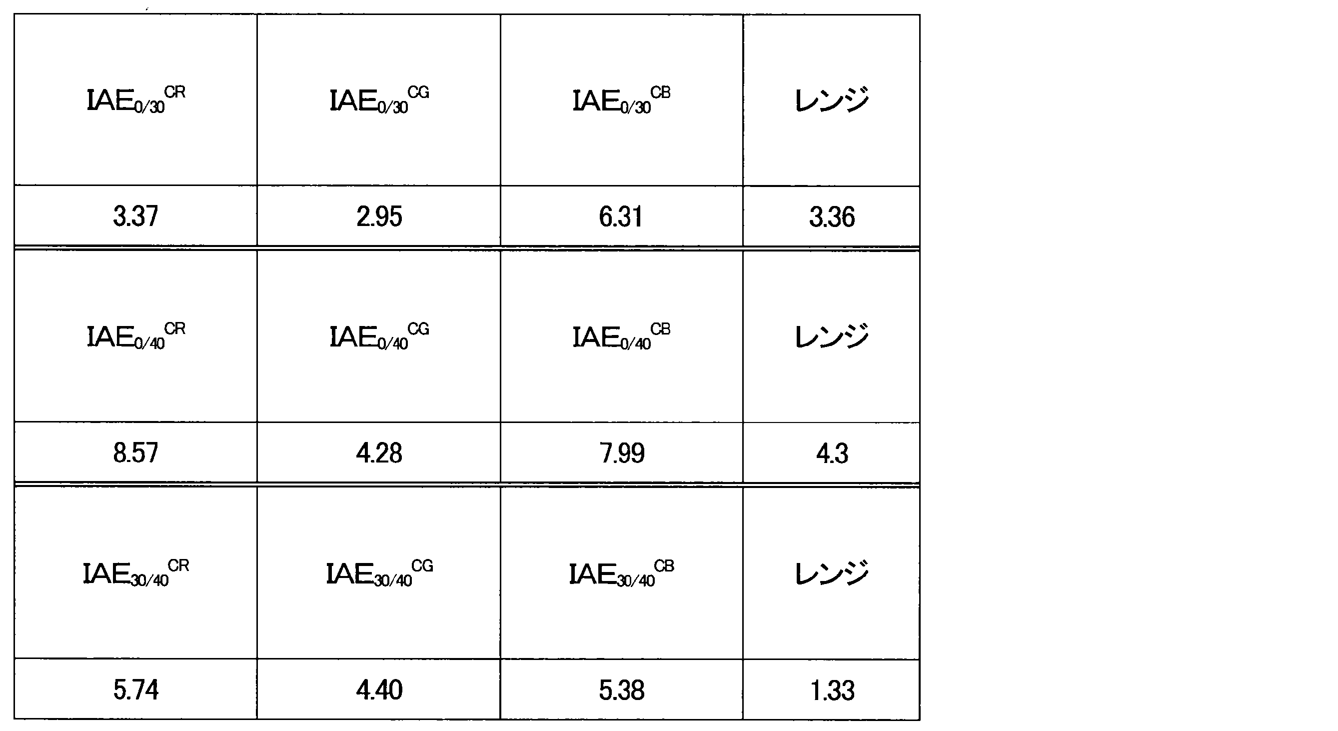


Claims (7)
- 光学フィルタであって、
近赤外線領域の少なくとも一部の光を吸収する光吸収剤を含有している光吸収層を備え、
0°、30°、及び40°の入射角度で波長300nm~1200nmの光を当該光学フィルタに入射させたときに、下記の条件を満たし、
(i)波長700nmにおける分光透過率が3%以下である。
(ii)波長715nmにおける分光透過率が1%以下である。
(iii)波長1100nmにおける分光透過率が7.5%以下である。
(iv)波長700nm~800nmにおける平均透過率が1%以下である。
(v)波長500nm~600nmにおける平均透過率が85%以上である。
(vi)波長400nmにおける分光透過率が45%以下である。
(vii)波長450nmにおける分光透過率が80%以上である。
入射角度がθ°であるときの波長λにおける当該光学フィルタの分光透過率をTθ(λ)と表し、
波長400nm~700nmの変域において表(I)によって定義される波長λの関数をR(λ)、G(λ)、及びB(λ)と表し、
T0(λ)と、R(λ)、G(λ)、及びB(λ)との積である3つの関数において、
最大値が1になるように正規化係数を定め、
Tθ(λ)と、R(λ)、G(λ)、及びB(λ)との積である関数に前記正規化係数を乗じて定まる関数をそれぞれCRθ(λ)、CGθ(λ)、及びCBθ(λ)と表し、
CRθ(λ)、CGθ(λ)、及びCBθ(λ)の変数である波長λを0以上の整数であるnの関数として、λ(n)=(Δλ×n+400)nmと表すとき(ただし、Δλ=5)、
0°、30°、及び40°から選ばれる2つの入射角度θ1°及びθ2°(θ1<θ2)に対して下記の式(1)~(3)によって定義されるIEθ1/θ2 CR、IEθ1/θ2 CG、及びIEθ1/θ2 CB及び同一の2つの入射角度θ1°及びθ2°に対するIEθ1/θ2 CR、IEθ1/θ2 CG、及びIEθ1/θ2 CBの最大値から最小値を差し引いた差であるレンジが表(II)に示す条件を満たす、
光学フィルタ。


- 0°、30°、及び40°から選ばれる2つの入射角度θ1°及びθ2°(θ1<θ2)に対して下記の式(4)~(6)によって定義されるIAEθ1/θ2 CR、IAEθ1/θ2 CG、及びIAEθ1/θ2 CB及び同一の2つの入射角度θ1°及びθ2°に対するIAEθ1/θ2 CR、IAEθ1/θ2 CG、及びIAEθ1/θ2 CBの最大値から最小値を差し引いた差であるレンジが表(III)に示す条件を満たす、請求項1に記載の光学フィルタ。


- 0°、30°、及び40°から選ばれる2つの入射角度θ1°及びθ2°(θ1<θ2)に対して下記の式(7)~(9)によって定義されるISEθ1/θ2 CR、ISEθ1/θ2 CG、及びISEθ1/θ2 CB及び同一の2つの入射角度θ1°及びθ2°に対するISEθ1/θ2 CR、ISEθ1/θ2 CG、及びISEθ1/θ2 CBの最大値から最小値を差し引いた差であるレンジが表(IV)に示す条件を満たす、請求項1又は2に記載の光学フィルタ。


- 前記光吸収剤は、ホスホン酸と銅イオンとによって形成されている、請求項1~3のいずれか1項に記載の光学フィルタ。
- 前記ホスホン酸は、アリール基を有する第一ホスホン酸を含む、請求項4に記載の光学フィルタ。
- 前記ホスホン酸は、さらに、アルキル基を有する第二ホスホン酸を含む、請求項5に記載の光学フィルタ。
- レンズ系と、
前記レンズ系を通過した光を受光する撮像素子と、
前記撮像素子の前方に配置され、R(赤)、G(緑)、及びB(青)の3色のフィルタを有するカラーフィルタと、
前記カラーフィルタの前方に配置された請求項1~6のいずれか1項に記載の光学フィルタと、を備えた、
撮像装置。
Priority Applications (3)
| Application Number | Priority Date | Filing Date | Title |
|---|---|---|---|
| KR1020207010315A KR102540605B1 (ko) | 2017-10-03 | 2018-09-19 | 광학 필터 및 촬상 장치 |
| US16/753,283 US11428857B2 (en) | 2017-10-03 | 2018-09-19 | Optical filter and imaging apparatus |
| CN201880064475.3A CN111164469B (zh) | 2017-10-03 | 2018-09-19 | 滤光器和摄像装置 |
Applications Claiming Priority (2)
| Application Number | Priority Date | Filing Date | Title |
|---|---|---|---|
| JP2017193904A JP6273063B1 (ja) | 2017-10-03 | 2017-10-03 | 光学フィルタ及び撮像装置 |
| JP2017-193904 | 2017-10-03 |
Publications (1)
| Publication Number | Publication Date |
|---|---|
| WO2019069687A1 true WO2019069687A1 (ja) | 2019-04-11 |
Family
ID=61074759
Family Applications (1)
| Application Number | Title | Priority Date | Filing Date |
|---|---|---|---|
| PCT/JP2018/034695 WO2019069687A1 (ja) | 2017-10-03 | 2018-09-19 | 光学フィルタ及び撮像装置 |
Country Status (6)
| Country | Link |
|---|---|
| US (1) | US11428857B2 (ja) |
| JP (1) | JP6273063B1 (ja) |
| KR (1) | KR102540605B1 (ja) |
| CN (1) | CN111164469B (ja) |
| TW (1) | TWI762722B (ja) |
| WO (1) | WO2019069687A1 (ja) |
Cited By (1)
| Publication number | Priority date | Publication date | Assignee | Title |
|---|---|---|---|---|
| CN113795559A (zh) * | 2019-05-23 | 2021-12-14 | 日本板硝子株式会社 | 光吸收性组合物、光吸收膜以及滤光器 |
Families Citing this family (4)
| Publication number | Priority date | Publication date | Assignee | Title |
|---|---|---|---|---|
| JP6259155B1 (ja) * | 2017-10-03 | 2018-01-10 | 日本板硝子株式会社 | 光学フィルタ及び撮像装置 |
| JP6273064B1 (ja) | 2017-10-03 | 2018-01-31 | 日本板硝子株式会社 | 光学フィルタ及び撮像装置 |
| KR102475669B1 (ko) * | 2020-09-22 | 2022-12-09 | 주식회사 창강화학 | 광학 필터 |
| WO2024048511A1 (ja) * | 2022-08-31 | 2024-03-07 | Agc株式会社 | 光学フィルタ |
Citations (5)
| Publication number | Priority date | Publication date | Assignee | Title |
|---|---|---|---|---|
| JP2012185468A (ja) * | 2010-12-17 | 2012-09-27 | Nippon Shokubai Co Ltd | 光選択透過フィルター、樹脂シート及び固体撮像素子 |
| WO2015111316A1 (ja) * | 2014-01-24 | 2015-07-30 | コニカミノルタ株式会社 | 撮像光学系,撮像光学装置及びデジタル機器 |
| WO2016114362A1 (ja) * | 2015-01-14 | 2016-07-21 | 旭硝子株式会社 | 近赤外線カットフィルタおよび固体撮像装置 |
| WO2017006571A1 (ja) * | 2015-07-09 | 2017-01-12 | 日本板硝子株式会社 | 赤外線カットフィルタ、撮像装置、及び赤外線カットフィルタの製造方法 |
| US20170146708A1 (en) * | 2014-02-12 | 2017-05-25 | Woo Joo LAH | Optical filter and imaging device comprising same |
Family Cites Families (27)
| Publication number | Priority date | Publication date | Assignee | Title |
|---|---|---|---|---|
| US4043248A (en) | 1976-06-10 | 1977-08-23 | General Electric Company | Liquid propellant gun (recoilless regenerative piston) |
| JPS6119920U (ja) | 1984-07-10 | 1986-02-05 | 三菱電機株式会社 | 押釦スイツチ |
| JPH0784123A (ja) * | 1993-09-13 | 1995-03-31 | Kureha Chem Ind Co Ltd | 光学フィルター |
| US6531230B1 (en) * | 1998-01-13 | 2003-03-11 | 3M Innovative Properties Company | Color shifting film |
| CN101606089A (zh) * | 2007-02-19 | 2009-12-16 | 三洋化成工业株式会社 | 多层结构粒子 |
| JP5936299B2 (ja) | 2010-11-08 | 2016-06-22 | Jsr株式会社 | 近赤外線カットフィルター、およびそれを備える固体撮像素子ならびに固体撮像装置 |
| KR101903518B1 (ko) * | 2011-02-24 | 2018-10-04 | 에이에스엠엘 네델란즈 비.브이. | 스침 입사 반사기, 리소그래피 장치, 스침 입사 반사기 제조 방법, 및 디바이스 제조 방법 |
| JP6036689B2 (ja) * | 2011-06-06 | 2016-11-30 | 旭硝子株式会社 | 光学フィルタ、固体撮像素子、撮像装置用レンズおよび撮像装置 |
| KR101677966B1 (ko) * | 2012-03-02 | 2016-11-21 | 후지필름 가부시키가이샤 | 착색 경화성 조성물 및 컬러필터 |
| WO2014002864A1 (ja) * | 2012-06-25 | 2014-01-03 | Jsr株式会社 | 固体撮像素子用光学フィルターおよびその用途 |
| CN104755969B (zh) | 2012-08-23 | 2018-06-08 | 旭硝子株式会社 | 近红外线截止滤波器和固体摄像装置 |
| JP6317875B2 (ja) * | 2012-09-06 | 2018-04-25 | 日本板硝子株式会社 | 赤外線カットフィルタ、撮像装置および赤外線カットフィルタの製造方法 |
| JP6241419B2 (ja) * | 2012-11-30 | 2017-12-06 | 旭硝子株式会社 | 近赤外線カットフィルタ |
| JP6248945B2 (ja) * | 2012-12-06 | 2017-12-20 | 旭硝子株式会社 | 近赤外線カットフィルタ |
| JP2014203044A (ja) | 2013-04-09 | 2014-10-27 | 日本板硝子株式会社 | 赤外線カットフィルタおよび撮像装置 |
| WO2014168221A1 (ja) * | 2013-04-11 | 2014-10-16 | 富士フイルム株式会社 | 近赤外線吸収性組成物、これを用いた近赤外線カットフィルタ及びその製造方法、並びに、カメラモジュール及びその製造方法 |
| KR101527822B1 (ko) | 2013-09-06 | 2015-06-10 | 주식회사 엘엠에스 | 광학 필터 및 이를 포함하는 촬상 장치 |
| JP6086885B2 (ja) * | 2013-09-30 | 2017-03-01 | 富士フイルム株式会社 | 着色組成物、硬化膜、カラーフィルタ、カラーフィルタの製造方法、固体撮像素子、画像表示装置および化合物 |
| JP6020746B2 (ja) * | 2013-12-26 | 2016-11-02 | 旭硝子株式会社 | 光学フィルタ |
| JP2016124903A (ja) * | 2014-12-26 | 2016-07-11 | 株式会社クレハ | 近赤外線吸収剤微粒子分散液の製造方法、近赤外線吸収剤微粒子分散液およびその用途 |
| WO2016114363A1 (ja) | 2015-01-14 | 2016-07-21 | 旭硝子株式会社 | 近赤外線カットフィルタおよび撮像装置 |
| KR20160088147A (ko) * | 2015-01-15 | 2016-07-25 | 주식회사 엘엠에스 | 근적외선 흡수층이 형성된 고체 촬상 장치용 커버글라스 |
| KR101780913B1 (ko) * | 2015-02-18 | 2017-09-21 | 아사히 가라스 가부시키가이샤 | 광학 필터 및 촬상 장치 |
| KR20180033114A (ko) * | 2015-07-28 | 2018-04-02 | 제이에스알 가부시끼가이샤 | 광학 필터 및 광학 필터를 구비하는 환경 광 센서 |
| JP6695887B2 (ja) * | 2015-09-24 | 2020-05-20 | 日本板硝子株式会社 | 赤外線吸収層用組成物、赤外線カットフィルタ、及び撮像装置 |
| CN105807353A (zh) * | 2016-05-24 | 2016-07-27 | 苏州大学 | 可见光及红外波段的宽波段吸收滤光结构及其制备方法 |
| JP6267823B1 (ja) * | 2017-07-27 | 2018-01-24 | 日本板硝子株式会社 | 光学フィルタ、カメラモジュール、及び情報端末 |
-
2017
- 2017-10-03 JP JP2017193904A patent/JP6273063B1/ja active Active
-
2018
- 2018-09-19 US US16/753,283 patent/US11428857B2/en active Active
- 2018-09-19 CN CN201880064475.3A patent/CN111164469B/zh active Active
- 2018-09-19 WO PCT/JP2018/034695 patent/WO2019069687A1/ja active Application Filing
- 2018-09-19 KR KR1020207010315A patent/KR102540605B1/ko active IP Right Grant
- 2018-09-21 TW TW107133413A patent/TWI762722B/zh active
Patent Citations (5)
| Publication number | Priority date | Publication date | Assignee | Title |
|---|---|---|---|---|
| JP2012185468A (ja) * | 2010-12-17 | 2012-09-27 | Nippon Shokubai Co Ltd | 光選択透過フィルター、樹脂シート及び固体撮像素子 |
| WO2015111316A1 (ja) * | 2014-01-24 | 2015-07-30 | コニカミノルタ株式会社 | 撮像光学系,撮像光学装置及びデジタル機器 |
| US20170146708A1 (en) * | 2014-02-12 | 2017-05-25 | Woo Joo LAH | Optical filter and imaging device comprising same |
| WO2016114362A1 (ja) * | 2015-01-14 | 2016-07-21 | 旭硝子株式会社 | 近赤外線カットフィルタおよび固体撮像装置 |
| WO2017006571A1 (ja) * | 2015-07-09 | 2017-01-12 | 日本板硝子株式会社 | 赤外線カットフィルタ、撮像装置、及び赤外線カットフィルタの製造方法 |
Cited By (2)
| Publication number | Priority date | Publication date | Assignee | Title |
|---|---|---|---|---|
| CN113795559A (zh) * | 2019-05-23 | 2021-12-14 | 日本板硝子株式会社 | 光吸收性组合物、光吸收膜以及滤光器 |
| CN113795559B (zh) * | 2019-05-23 | 2022-08-30 | 日本板硝子株式会社 | 光吸收性组合物、光吸收膜以及滤光器 |
Also Published As
| Publication number | Publication date |
|---|---|
| CN111164469A (zh) | 2020-05-15 |
| JP6273063B1 (ja) | 2018-01-31 |
| CN111164469B (zh) | 2022-01-11 |
| TW201928414A (zh) | 2019-07-16 |
| KR20200064086A (ko) | 2020-06-05 |
| TWI762722B (zh) | 2022-05-01 |
| KR102540605B1 (ko) | 2023-06-07 |
| US20200333516A1 (en) | 2020-10-22 |
| JP2019066742A (ja) | 2019-04-25 |
| US11428857B2 (en) | 2022-08-30 |
Similar Documents
| Publication | Publication Date | Title |
|---|---|---|
| JP6538294B1 (ja) | 光学フィルタ及び撮像装置 | |
| WO2018003756A1 (ja) | 赤外線カットフィルタ及び撮像光学系 | |
| WO2019069689A1 (ja) | 光学フィルタ及び撮像装置 | |
| WO2019069687A1 (ja) | 光学フィルタ及び撮像装置 | |
| WO2019111965A1 (ja) | 光学フィルタ及び撮像装置 | |
| WO2019138976A1 (ja) | 光学フィルタ及び撮像装置 | |
| JP6966334B2 (ja) | 光学フィルタ及び撮像装置 | |
| WO2019069688A1 (ja) | 光学フィルタ及び撮像装置 | |
| JP6259156B1 (ja) | 光学フィルタ及び撮像装置 | |
| JP6259157B1 (ja) | 光学フィルタ及び撮像装置 | |
| JP6273062B1 (ja) | 光学フィルタ及び撮像装置 | |
| JP6516948B1 (ja) | 光学フィルタ及び撮像装置 |
Legal Events
| Date | Code | Title | Description |
|---|---|---|---|
| 121 | Ep: the epo has been informed by wipo that ep was designated in this application |
Ref document number: 18865288 Country of ref document: EP Kind code of ref document: A1 |
|
| NENP | Non-entry into the national phase |
Ref country code: DE |
|
| ENP | Entry into the national phase |
Ref document number: 20207010315 Country of ref document: KR Kind code of ref document: A |
|
| 122 | Ep: pct application non-entry in european phase |
Ref document number: 18865288 Country of ref document: EP Kind code of ref document: A1 |