WO2019111965A1 - 光学フィルタ及び撮像装置 - Google Patents
光学フィルタ及び撮像装置 Download PDFInfo
- Publication number
- WO2019111965A1 WO2019111965A1 PCT/JP2018/044776 JP2018044776W WO2019111965A1 WO 2019111965 A1 WO2019111965 A1 WO 2019111965A1 JP 2018044776 W JP2018044776 W JP 2018044776W WO 2019111965 A1 WO2019111965 A1 WO 2019111965A1
- Authority
- WO
- WIPO (PCT)
- Prior art keywords
- optical filter
- light
- wavelength
- spectral transmittance
- filter according
- Prior art date
Links
- 230000003287 optical effect Effects 0.000 title claims abstract description 288
- 238000003384 imaging method Methods 0.000 title claims description 89
- 238000002834 transmittance Methods 0.000 claims abstract description 231
- 230000003595 spectral effect Effects 0.000 claims abstract description 204
- 239000006096 absorbing agent Substances 0.000 claims description 39
- ABLZXFCXXLZCGV-UHFFFAOYSA-N Phosphorous acid Chemical compound OP(O)=O ABLZXFCXXLZCGV-UHFFFAOYSA-N 0.000 claims description 29
- JPVYNHNXODAKFH-UHFFFAOYSA-N Cu2+ Chemical compound [Cu+2] JPVYNHNXODAKFH-UHFFFAOYSA-N 0.000 claims description 10
- 125000003118 aryl group Chemical group 0.000 claims description 10
- 229910001431 copper ion Inorganic materials 0.000 claims description 10
- 125000000217 alkyl group Chemical group 0.000 claims description 9
- 239000000243 solution Substances 0.000 description 187
- 239000010410 layer Substances 0.000 description 152
- 239000000758 substrate Substances 0.000 description 86
- WYURNTSHIVDZCO-UHFFFAOYSA-N Tetrahydrofuran Chemical compound C1CCOC1 WYURNTSHIVDZCO-UHFFFAOYSA-N 0.000 description 64
- 239000011248 coating agent Substances 0.000 description 61
- 238000000576 coating method Methods 0.000 description 61
- 238000000411 transmission spectrum Methods 0.000 description 57
- 230000031700 light absorption Effects 0.000 description 52
- 239000011521 glass Substances 0.000 description 51
- 239000000203 mixture Substances 0.000 description 51
- 230000000052 comparative effect Effects 0.000 description 43
- 229920005989 resin Polymers 0.000 description 43
- 239000011347 resin Substances 0.000 description 43
- YXFVVABEGXRONW-UHFFFAOYSA-N Toluene Chemical compound CC1=CC=CC=C1 YXFVVABEGXRONW-UHFFFAOYSA-N 0.000 description 42
- YLQBMQCUIZJEEH-UHFFFAOYSA-N tetrahydrofuran Natural products C=1C=COC=1 YLQBMQCUIZJEEH-UHFFFAOYSA-N 0.000 description 32
- -1 phosphate ester Chemical class 0.000 description 30
- 239000000047 product Substances 0.000 description 24
- 239000002904 solvent Substances 0.000 description 22
- ZWEHNKRNPOVVGH-UHFFFAOYSA-N 2-Butanone Chemical compound CCC(C)=O ZWEHNKRNPOVVGH-UHFFFAOYSA-N 0.000 description 21
- 239000007788 liquid Substances 0.000 description 18
- 239000011159 matrix material Substances 0.000 description 18
- 229920002050 silicone resin Polymers 0.000 description 18
- 238000003756 stirring Methods 0.000 description 16
- 230000035945 sensitivity Effects 0.000 description 15
- 229910019142 PO4 Inorganic materials 0.000 description 14
- 238000010438 heat treatment Methods 0.000 description 14
- 239000010452 phosphate Substances 0.000 description 14
- 230000003667 anti-reflective effect Effects 0.000 description 13
- OPQARKPSCNTWTJ-UHFFFAOYSA-L copper(ii) acetate Chemical compound [Cu+2].CC([O-])=O.CC([O-])=O OPQARKPSCNTWTJ-UHFFFAOYSA-L 0.000 description 12
- 239000010419 fine particle Substances 0.000 description 12
- 239000011265 semifinished product Substances 0.000 description 11
- 239000000126 substance Substances 0.000 description 11
- NWFNSTOSIVLCJA-UHFFFAOYSA-L copper;diacetate;hydrate Chemical compound O.[Cu+2].CC([O-])=O.CC([O-])=O NWFNSTOSIVLCJA-UHFFFAOYSA-L 0.000 description 10
- 238000004807 desolvation Methods 0.000 description 10
- CPUDPFPXCZDNGI-UHFFFAOYSA-N triethoxy(methyl)silane Chemical compound CCO[Si](C)(OCC)OCC CPUDPFPXCZDNGI-UHFFFAOYSA-N 0.000 description 10
- 238000010521 absorption reaction Methods 0.000 description 9
- 238000013461 design Methods 0.000 description 9
- 239000000178 monomer Substances 0.000 description 9
- 125000001997 phenyl group Chemical group [H]C1=C([H])C([H])=C(*)C([H])=C1[H] 0.000 description 9
- 230000005540 biological transmission Effects 0.000 description 8
- 150000001879 copper Chemical class 0.000 description 8
- 239000011241 protective layer Substances 0.000 description 8
- 238000001228 spectrum Methods 0.000 description 8
- 229910004298 SiO 2 Inorganic materials 0.000 description 7
- BOTDANWDWHJENH-UHFFFAOYSA-N Tetraethyl orthosilicate Chemical compound CCO[Si](OCC)(OCC)OCC BOTDANWDWHJENH-UHFFFAOYSA-N 0.000 description 7
- 239000010949 copper Substances 0.000 description 7
- 229920002037 poly(vinyl butyral) polymer Polymers 0.000 description 7
- 229920003171 Poly (ethylene oxide) Polymers 0.000 description 6
- 238000009835 boiling Methods 0.000 description 6
- 239000006185 dispersion Substances 0.000 description 6
- 239000006059 cover glass Substances 0.000 description 5
- 230000007062 hydrolysis Effects 0.000 description 5
- 238000006460 hydrolysis reaction Methods 0.000 description 5
- 239000000463 material Substances 0.000 description 5
- 238000000034 method Methods 0.000 description 5
- 150000003014 phosphoric acid esters Chemical class 0.000 description 5
- 238000012643 polycondensation polymerization Methods 0.000 description 5
- 229910052594 sapphire Inorganic materials 0.000 description 5
- 239000010980 sapphire Substances 0.000 description 5
- RYGMFSIKBFXOCR-UHFFFAOYSA-N Copper Chemical compound [Cu] RYGMFSIKBFXOCR-UHFFFAOYSA-N 0.000 description 4
- CTQNGGLPUBDAKN-UHFFFAOYSA-N O-Xylene Chemical group CC1=CC=CC=C1C CTQNGGLPUBDAKN-UHFFFAOYSA-N 0.000 description 4
- QLZHNIAADXEJJP-UHFFFAOYSA-N Phenylphosphonic acid Chemical compound OP(O)(=O)C1=CC=CC=C1 QLZHNIAADXEJJP-UHFFFAOYSA-N 0.000 description 4
- 229910010413 TiO 2 Inorganic materials 0.000 description 4
- 239000005388 borosilicate glass Substances 0.000 description 4
- UOKRBSXOBUKDGE-UHFFFAOYSA-N butylphosphonic acid Chemical compound CCCCP(O)(O)=O UOKRBSXOBUKDGE-UHFFFAOYSA-N 0.000 description 4
- 230000008859 change Effects 0.000 description 4
- 229910052802 copper Inorganic materials 0.000 description 4
- 238000012937 correction Methods 0.000 description 4
- 125000000524 functional group Chemical group 0.000 description 4
- 238000007740 vapor deposition Methods 0.000 description 4
- XDGIQCFWQNHSMV-UHFFFAOYSA-N (4-bromophenyl)phosphonic acid Chemical compound OP(O)(=O)C1=CC=C(Br)C=C1 XDGIQCFWQNHSMV-UHFFFAOYSA-N 0.000 description 3
- QTBSBXVTEAMEQO-UHFFFAOYSA-N Acetic acid Chemical compound CC(O)=O QTBSBXVTEAMEQO-UHFFFAOYSA-N 0.000 description 3
- 229920000178 Acrylic resin Polymers 0.000 description 3
- 239000004925 Acrylic resin Substances 0.000 description 3
- 102100026353 F-box-like/WD repeat-containing protein TBL1XR1 Human genes 0.000 description 3
- 101000835675 Homo sapiens F-box-like/WD repeat-containing protein TBL1XR1 Proteins 0.000 description 3
- 239000004962 Polyamide-imide Substances 0.000 description 3
- 239000004695 Polyether sulfone Substances 0.000 description 3
- 101100341123 Saccharomyces cerevisiae (strain ATCC 204508 / S288c) IRA2 gene Proteins 0.000 description 3
- RRJHFUHAKCSNRY-UHFFFAOYSA-L [Cu+2].[O-]P([O-])=O Chemical compound [Cu+2].[O-]P([O-])=O RRJHFUHAKCSNRY-UHFFFAOYSA-L 0.000 description 3
- 239000011358 absorbing material Substances 0.000 description 3
- 125000001797 benzyl group Chemical group [H]C1=C([H])C([H])=C(C([H])=C1[H])C([H])([H])* 0.000 description 3
- WYKCOLQQHSQKIU-UHFFFAOYSA-L copper butyl-dioxido-oxo-lambda5-phosphane Chemical compound [Cu++].CCCCP([O-])([O-])=O WYKCOLQQHSQKIU-UHFFFAOYSA-L 0.000 description 3
- WOYKGBHMRHXOCY-UHFFFAOYSA-L copper;(4-bromophenyl)-dioxido-oxo-$l^{5}-phosphane Chemical compound [Cu+2].[O-]P([O-])(=O)C1=CC=C(Br)C=C1 WOYKGBHMRHXOCY-UHFFFAOYSA-L 0.000 description 3
- DHGSSULXZRNIPW-UHFFFAOYSA-L copper;dioxido-oxo-phenyl-$l^{5}-phosphane Chemical compound [Cu+2].[O-]P([O-])(=O)C1=CC=CC=C1 DHGSSULXZRNIPW-UHFFFAOYSA-L 0.000 description 3
- 230000000694 effects Effects 0.000 description 3
- 239000003822 epoxy resin Substances 0.000 description 3
- 238000010030 laminating Methods 0.000 description 3
- 238000004519 manufacturing process Methods 0.000 description 3
- 238000005259 measurement Methods 0.000 description 3
- 238000002454 metastable transfer emission spectrometry Methods 0.000 description 3
- 238000002156 mixing Methods 0.000 description 3
- NBIIXXVUZAFLBC-UHFFFAOYSA-K phosphate Chemical compound [O-]P([O-])([O-])=O NBIIXXVUZAFLBC-UHFFFAOYSA-K 0.000 description 3
- 229920002492 poly(sulfone) Polymers 0.000 description 3
- 229920006122 polyamide resin Polymers 0.000 description 3
- 229920002312 polyamide-imide Polymers 0.000 description 3
- 229920005668 polycarbonate resin Polymers 0.000 description 3
- 239000004431 polycarbonate resin Substances 0.000 description 3
- 229920000647 polyepoxide Polymers 0.000 description 3
- 229920006393 polyether sulfone Polymers 0.000 description 3
- 229920001721 polyimide Polymers 0.000 description 3
- 239000009719 polyimide resin Substances 0.000 description 3
- 229920005672 polyolefin resin Polymers 0.000 description 3
- 239000007787 solid Substances 0.000 description 3
- 238000004528 spin coating Methods 0.000 description 3
- 238000007738 vacuum evaporation Methods 0.000 description 3
- 238000010792 warming Methods 0.000 description 3
- SIKJAQJRHWYJAI-UHFFFAOYSA-N Indole Chemical compound C1=CC=C2NC=CC2=C1 SIKJAQJRHWYJAI-UHFFFAOYSA-N 0.000 description 2
- 230000009471 action Effects 0.000 description 2
- 150000008366 benzophenones Chemical class 0.000 description 2
- 230000000903 blocking effect Effects 0.000 description 2
- 125000004432 carbon atom Chemical group C* 0.000 description 2
- 239000003795 chemical substances by application Substances 0.000 description 2
- RTZKZFJDLAIYFH-UHFFFAOYSA-N ether Substances CCOCC RTZKZFJDLAIYFH-UHFFFAOYSA-N 0.000 description 2
- 239000005303 fluorophosphate glass Substances 0.000 description 2
- 125000005843 halogen group Chemical group 0.000 description 2
- 125000004435 hydrogen atom Chemical group [H]* 0.000 description 2
- 229940078552 o-xylene Drugs 0.000 description 2
- 125000005429 oxyalkyl group Chemical group 0.000 description 2
- 230000002093 peripheral effect Effects 0.000 description 2
- 239000005365 phosphate glass Substances 0.000 description 2
- 125000004437 phosphorous atom Chemical group 0.000 description 2
- 229910052698 phosphorus Inorganic materials 0.000 description 2
- 230000008569 process Effects 0.000 description 2
- 230000001681 protective effect Effects 0.000 description 2
- ANRHNWWPFJCPAZ-UHFFFAOYSA-M thionine Chemical compound [Cl-].C1=CC(N)=CC2=[S+]C3=CC(N)=CC=C3N=C21 ANRHNWWPFJCPAZ-UHFFFAOYSA-M 0.000 description 2
- 239000006097 ultraviolet radiation absorber Substances 0.000 description 2
- JYEUMXHLPRZUAT-UHFFFAOYSA-N 1,2,3-triazine Chemical compound C1=CN=NN=C1 JYEUMXHLPRZUAT-UHFFFAOYSA-N 0.000 description 1
- KRHYYFGTRYWZRS-UHFFFAOYSA-M Fluoride anion Chemical compound [F-] KRHYYFGTRYWZRS-UHFFFAOYSA-M 0.000 description 1
- 241000511976 Hoya Species 0.000 description 1
- ZCQWOFVYLHDMMC-UHFFFAOYSA-N Oxazole Chemical compound C1=COC=N1 ZCQWOFVYLHDMMC-UHFFFAOYSA-N 0.000 description 1
- 229910000831 Steel Inorganic materials 0.000 description 1
- RWCCWEUUXYIKHB-UHFFFAOYSA-N benzophenone Chemical compound C=1C=CC=CC=1C(=O)C1=CC=CC=C1 RWCCWEUUXYIKHB-UHFFFAOYSA-N 0.000 description 1
- 239000012965 benzophenone Substances 0.000 description 1
- 238000005282 brightening Methods 0.000 description 1
- 229910052799 carbon Inorganic materials 0.000 description 1
- 238000005266 casting Methods 0.000 description 1
- 239000003086 colorant Substances 0.000 description 1
- 230000000295 complement effect Effects 0.000 description 1
- 150000001875 compounds Chemical class 0.000 description 1
- 238000009833 condensation Methods 0.000 description 1
- 230000005494 condensation Effects 0.000 description 1
- 239000007859 condensation product Substances 0.000 description 1
- 150000004696 coordination complex Chemical class 0.000 description 1
- RYGMFSIKBFXOCR-AHCXROLUSA-N copper-60 Chemical compound [60Cu] RYGMFSIKBFXOCR-AHCXROLUSA-N 0.000 description 1
- 230000006866 deterioration Effects 0.000 description 1
- 238000007607 die coating method Methods 0.000 description 1
- 239000003989 dielectric material Substances 0.000 description 1
- OTARVPUIYXHRRB-UHFFFAOYSA-N diethoxy-methyl-[3-(oxiran-2-ylmethoxy)propyl]silane Chemical compound CCO[Si](C)(OCC)CCCOCC1CO1 OTARVPUIYXHRRB-UHFFFAOYSA-N 0.000 description 1
- JJQZDUKDJDQPMQ-UHFFFAOYSA-N dimethoxy(dimethyl)silane Chemical compound CO[Si](C)(C)OC JJQZDUKDJDQPMQ-UHFFFAOYSA-N 0.000 description 1
- YYLGKUPAFFKGRQ-UHFFFAOYSA-N dimethyldiethoxysilane Chemical compound CCO[Si](C)(C)OCC YYLGKUPAFFKGRQ-UHFFFAOYSA-N 0.000 description 1
- 238000010494 dissociation reaction Methods 0.000 description 1
- 230000005593 dissociations Effects 0.000 description 1
- 238000001035 drying Methods 0.000 description 1
- 150000002148 esters Chemical class 0.000 description 1
- 239000005357 flat glass Substances 0.000 description 1
- LNEPOXFFQSENCJ-UHFFFAOYSA-N haloperidol Chemical compound C1CC(O)(C=2C=CC(Cl)=CC=2)CCN1CCCC(=O)C1=CC=C(F)C=C1 LNEPOXFFQSENCJ-UHFFFAOYSA-N 0.000 description 1
- 230000003301 hydrolyzing effect Effects 0.000 description 1
- 125000004464 hydroxyphenyl group Chemical group 0.000 description 1
- PZOUSPYUWWUPPK-UHFFFAOYSA-N indole Natural products CC1=CC=CC2=C1C=CN2 PZOUSPYUWWUPPK-UHFFFAOYSA-N 0.000 description 1
- RKJUIXBNRJVNHR-UHFFFAOYSA-N indolenine Natural products C1=CC=C2CC=NC2=C1 RKJUIXBNRJVNHR-UHFFFAOYSA-N 0.000 description 1
- 230000003993 interaction Effects 0.000 description 1
- 239000000395 magnesium oxide Substances 0.000 description 1
- CPLXHLVBOLITMK-UHFFFAOYSA-N magnesium oxide Inorganic materials [Mg]=O CPLXHLVBOLITMK-UHFFFAOYSA-N 0.000 description 1
- AXZKOIWUVFPNLO-UHFFFAOYSA-N magnesium;oxygen(2-) Chemical compound [O-2].[Mg+2] AXZKOIWUVFPNLO-UHFFFAOYSA-N 0.000 description 1
- DZVCFNFOPIZQKX-LTHRDKTGSA-M merocyanine Chemical compound [Na+].O=C1N(CCCC)C(=O)N(CCCC)C(=O)C1=C\C=C\C=C/1N(CCCS([O-])(=O)=O)C2=CC=CC=C2O\1 DZVCFNFOPIZQKX-LTHRDKTGSA-M 0.000 description 1
- 229910052751 metal Inorganic materials 0.000 description 1
- 239000002184 metal Substances 0.000 description 1
- 229910044991 metal oxide Inorganic materials 0.000 description 1
- 150000004706 metal oxides Chemical class 0.000 description 1
- ARYZCSRUUPFYMY-UHFFFAOYSA-N methoxysilane Chemical compound CO[SiH3] ARYZCSRUUPFYMY-UHFFFAOYSA-N 0.000 description 1
- BFXIKLCIZHOAAZ-UHFFFAOYSA-N methyltrimethoxysilane Chemical compound CO[Si](C)(OC)OC BFXIKLCIZHOAAZ-UHFFFAOYSA-N 0.000 description 1
- 230000004048 modification Effects 0.000 description 1
- 238000012986 modification Methods 0.000 description 1
- 125000006501 nitrophenyl group Chemical group 0.000 description 1
- 230000035699 permeability Effects 0.000 description 1
- RCMHUQGSSVZPDG-UHFFFAOYSA-N phenoxybenzene;phosphoric acid Chemical class OP(O)(O)=O.C=1C=CC=CC=1OC1=CC=CC=C1 RCMHUQGSSVZPDG-UHFFFAOYSA-N 0.000 description 1
- 150000003009 phosphonic acids Chemical class 0.000 description 1
- IEQIEDJGQAUEQZ-UHFFFAOYSA-N phthalocyanine Chemical compound N1C(N=C2C3=CC=CC=C3C(N=C3C4=CC=CC=C4C(=N4)N3)=N2)=C(C=CC=C2)C2=C1N=C1C2=CC=CC=C2C4=N1 IEQIEDJGQAUEQZ-UHFFFAOYSA-N 0.000 description 1
- 229920000642 polymer Polymers 0.000 description 1
- 239000010453 quartz Substances 0.000 description 1
- 230000009467 reduction Effects 0.000 description 1
- 239000012266 salt solution Substances 0.000 description 1
- 230000003678 scratch resistant effect Effects 0.000 description 1
- 239000004065 semiconductor Substances 0.000 description 1
- VYPSYNLAJGMNEJ-UHFFFAOYSA-N silicon dioxide Inorganic materials O=[Si]=O VYPSYNLAJGMNEJ-UHFFFAOYSA-N 0.000 description 1
- 239000002356 single layer Substances 0.000 description 1
- 239000005361 soda-lime glass Substances 0.000 description 1
- 229910001220 stainless steel Inorganic materials 0.000 description 1
- 239000010935 stainless steel Substances 0.000 description 1
- 239000010959 steel Substances 0.000 description 1
- LFQCEHFDDXELDD-UHFFFAOYSA-N tetramethyl orthosilicate Chemical compound CO[Si](OC)(OC)OC LFQCEHFDDXELDD-UHFFFAOYSA-N 0.000 description 1
- 125000005425 toluyl group Chemical group 0.000 description 1
- JCVQKRGIASEUKR-UHFFFAOYSA-N triethoxy(phenyl)silane Chemical compound CCO[Si](OCC)(OCC)C1=CC=CC=C1 JCVQKRGIASEUKR-UHFFFAOYSA-N 0.000 description 1
- JXUKBNICSRJFAP-UHFFFAOYSA-N triethoxy-[3-(oxiran-2-ylmethoxy)propyl]silane Chemical compound CCO[Si](OCC)(OCC)CCCOCC1CO1 JXUKBNICSRJFAP-UHFFFAOYSA-N 0.000 description 1
- ZNOCGWVLWPVKAO-UHFFFAOYSA-N trimethoxy(phenyl)silane Chemical compound CO[Si](OC)(OC)C1=CC=CC=C1 ZNOCGWVLWPVKAO-UHFFFAOYSA-N 0.000 description 1
- 230000000007 visual effect Effects 0.000 description 1
Images


Classifications
-
- G—PHYSICS
- G02—OPTICS
- G02B—OPTICAL ELEMENTS, SYSTEMS OR APPARATUS
- G02B5/00—Optical elements other than lenses
- G02B5/20—Filters
- G02B5/208—Filters for use with infrared or ultraviolet radiation, e.g. for separating visible light from infrared and/or ultraviolet radiation
-
- G—PHYSICS
- G02—OPTICS
- G02B—OPTICAL ELEMENTS, SYSTEMS OR APPARATUS
- G02B5/00—Optical elements other than lenses
- G02B5/20—Filters
- G02B5/22—Absorbing filters
- G02B5/223—Absorbing filters containing organic substances, e.g. dyes, inks or pigments
-
- G—PHYSICS
- G02—OPTICS
- G02B—OPTICAL ELEMENTS, SYSTEMS OR APPARATUS
- G02B5/00—Optical elements other than lenses
- G02B5/20—Filters
- G02B5/28—Interference filters
- G02B5/281—Interference filters designed for the infrared light
- G02B5/282—Interference filters designed for the infrared light reflecting for infrared and transparent for visible light, e.g. heat reflectors, laser protection
-
- H—ELECTRICITY
- H04—ELECTRIC COMMUNICATION TECHNIQUE
- H04N—PICTORIAL COMMUNICATION, e.g. TELEVISION
- H04N23/00—Cameras or camera modules comprising electronic image sensors; Control thereof
- H04N23/50—Constructional details
- H04N23/55—Optical parts specially adapted for electronic image sensors; Mounting thereof
Definitions
- the present invention relates to an optical filter and an imaging device.
- Patent Document 1 describes a near-infrared cut filter including a laminate having a resin layer containing a near-infrared absorber on at least one side of a glass substrate.
- this near infrared cut filter has a dielectric multilayer film on at least one side of a laminate.
- of the difference between the wavelength value (Ya) and the wavelength value (Yb) is less than 15 nm.
- the value of the wavelength (Ya) is a value of the wavelength at which the transmittance is 50% when measured from the vertical direction of the near infrared cut filter in the wavelength range of 560 to 800 nm.
- the wavelength value (Yb) is a wavelength value at which the transmittance is 50% when measured from an angle of 30 ° with respect to the vertical direction of the near infrared cut filter in the wavelength range of 560 to 800 nm.
- Patent Document 2 describes a near-infrared cut filter provided with a near-infrared absorbing glass substrate, a near-infrared absorbing layer, and a dielectric multilayer film.
- the near infrared absorbing layer contains a near infrared absorbing dye and a transparent resin.
- Patent Document 2 describes a solid-state imaging device including the near-infrared cut filter and a solid-state imaging device. According to Patent Document 2, by laminating a near-infrared absorbing glass substrate and a near-infrared absorbing layer, an incident angle dependency in which the shielding wavelength is shifted depending on the incident angle of light inherently possessed by the dielectric multilayer film. Can almost eliminate the influence of For example, in Patent Document 2, the transmittance (T 0 ) at an incident angle of 0 ° and the transmittance (T 30 ) at an incident angle of 30 ° in a near infrared cut filter are measured.
- Patent Documents 3 and 4 disclose an infrared cut filter including a transparent dielectric substrate, an infrared reflection layer, and an infrared absorption layer.
- the infrared reflection layer is formed of a dielectric multilayer film.
- the infrared absorbing layer contains an infrared absorbing dye.
- Patent Documents 3 and 4 describe an imaging device provided with this infrared cut filter.
- Patent Documents 3 and 4 describe the transmittance spectrum of the infrared cut filter when the incident angle of light is 0 °, 25 °, and 35 °.
- JP 2012-103340 A International Publication No. 2014/030628 JP, 2014-52482, A JP, 2014-203044, A
- the present invention is an optical system capable of shielding unnecessary light and having an advantageous characteristic to prevent the occurrence of color unevenness in the image generated by the imaging device even when the incident angle of light is large.
- a filter Provides a filter.
- the present invention also provides an imaging device provided with this optical filter.
- the present invention An optical filter, A light absorbing layer containing a light absorbing agent that absorbs at least part of light in the near infrared region,
- the spectral transmittance at a wavelength of 380 nm is 20% or less.
- the spectral transmittance at a wavelength of 450 nm is 75% or more.
- the average value of the spectral transmittance in the wavelength range of 500 to 600 nm is 80% or more.
- the spectral transmittance at a wavelength of 700 nm is 5% or less.
- the spectral transmittance at a wavelength of 715 nm is 3% or less.
- the average value of spectral transmittance in the wavelength range of 700 to 800 nm is 1% or less.
- the maximum value of the spectral transmittance in the wavelength range of 750 to 1080 nm is 1% or less.
- the maximum value of the spectral transmittance in the wavelength range of 1000 to 1100 nm is 2% or less.
- the wavelength band width of the wavelength band showing a spectral transmittance of 75% or more in the wavelength range of 400 to 700 nm is 170 nm or more.
- the normalized spectral transmittance is determined by normalizing the spectral transmittance at each of the incident angles such that the maximum value in the wavelength range of 400 to 650 nm of the spectral transmitt
- the present invention is Lens system, An imaging element that receives light passing through the lens system; And the above-described optical filter disposed in front of the image sensor.
- An imaging device is provided.
- the above-mentioned optical filter can shield unnecessary light rays and has advantageous characteristics for preventing the occurrence of color unevenness in the image generated by the imaging device even when the incident angle of light is large. Further, in the above-described imaging device, color unevenness hardly occurs in the generated image.
- FIG. 1A is a cross-sectional view showing an example of the optical filter of the present invention.
- FIG. 1B is a cross-sectional view showing another example of the optical filter of the present invention.
- FIG. 1C is a cross-sectional view showing still another example of the optical filter of the present invention.
- FIG. 1D is a cross-sectional view showing still another example of the optical filter of the present invention.
- FIG. 1E is a cross-sectional view showing still another example of the optical filter of the present invention.
- FIG. 2 is a cross-sectional view showing an example of an imaging device according to the present invention.
- FIG. 3A is a transmittance spectrum of the optical filter according to Example 1 when the incident angles of light are 0 °, 30 °, 35 °, and 40 °.
- FIG. 3B is a transmittance spectrum of the optical filter according to Example 1 when the incident angles of light are 45 °, 50 °, 55 °, 60 °, and 65 °.
- FIG. 4A is a graph showing the normalized spectral transmittance of the optical filter according to Example 1 when the incident angles of light are 0 °, 30 °, 35 °, and 40 °.
- FIG. 4B is a graph showing the normalized spectral transmittance of the optical filter according to Example 1 when the incident angles of light are 45 °, 50 °, 55 °, 60 °, and 65 °.
- FIG. 4A is a graph showing the normalized spectral transmittance of the optical filter according to Example 1 when the incident angles of light are 0 °, 30 °, 35 °, and 40 °.
- FIG. 4B is a graph showing the normalized spectral transmittance of the optical filter according to Example 1 when the incident angles of light are 45 °, 50 °, 55
- FIG. 5A is a transmittance spectrum of the optical filter according to Example 2 when the incident angles of light are 0 °, 30 °, 35 °, and 40 °.
- FIG. 5B is a transmittance spectrum of the optical filter according to Example 2 when the incident angles of light are 45 °, 50 °, 55 °, 60 °, and 65 °.
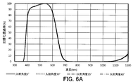
- FIG. 6A is a graph showing the normalized spectral transmittance of the optical filter according to Example 2 when the incident angles of light are 0 °, 30 °, 35 °, and 40 °.
- FIG. 6B is a graph showing the normalized spectral transmittance of the optical filter according to Example 2 when the incident angles of light are 45 °, 50 °, 55 °, 60 °, and 65 °.
- FIG. 7A is a transmittance spectrum of the optical filter according to Example 3 when the incident angles of light are 0 °, 30 °, 35 °, and 40 °.
- FIG. 7B is a transmittance spectrum of the optical filter according to Example 3 when the incident angles of light are 45 °, 50 °, 55 °, 60 °, and 65 °.
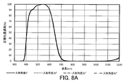
- FIG. 8A is a graph showing the normalized spectral transmittance of the optical filter according to Example 3 when the incident angles of light are 0 °, 30 °, 35 °, and 40 °.
- FIG. 8B is a graph showing the normalized spectral transmittance of the optical filter according to Example 3 when the incident angles of light are 45 °, 50 °, 55 °, 60 °, and 65 °.
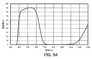
- FIG. 9A is a transmittance spectrum of a semifinished product of the optical filter according to Example 4 when the incident angle of light is 0 °.
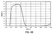
- FIG. 9B is a transmittance spectrum of another semifinished product of the optical filter according to Example 4 when the incident angle of light is 0 °.
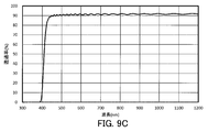
- FIG. 9C is a transmittance spectrum of the laminate according to Reference Example 1 when the incident angle of light is 0 °.
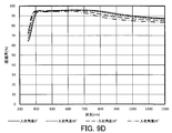
- FIG. 9D is a transmittance spectrum of a laminate according to Reference Example 2 when incident angles of light are 0 °, 30 °, 50 °, and 65 °.
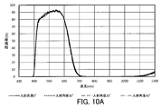
- FIG. 10A is a transmittance spectrum of the optical filter according to Example 4 when the incident angles of light are 0 °, 30 °, 35 °, and 40 °.
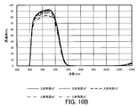
- FIG. 10B is a transmittance spectrum of the optical filter according to Example 4 when the incident angles of light are 45 °, 50 °, 55 °, 60 °, and 65 °.
- FIG. 11A is a graph showing the normalized spectral transmittance of the optical filter according to Example 4 when the incident angles of light are 0 °, 30 °, 35 °, and 40 °.
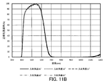
- FIG. 11B is a graph showing the normalized spectral transmittance of the optical filter according to Example 4 when the incident angles of light are 45 °, 50 °, 55 °, 60 °, and 65 °.
- FIG. 12A is a transmittance spectrum of the semi-finished product of the optical filter according to Comparative Example 1 when the incident angles of light are 0 °, 30 °, and 50 °.
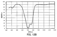
- FIG. 12B is a transmittance spectrum of the laminate according to Reference Example 3 when the incident angle of light is 0 °.
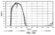
- FIG. 13A is a transmittance spectrum of the optical filter according to Comparative Example 1 when the incident angles of light are 0 °, 30 °, 35 °, and 40 °.
- FIG. 13B is a transmittance spectrum of the optical filter according to Comparative Example 1 when the incident angles of light are 45 °, 50 °, 55 °, 60 °, and 65 °.
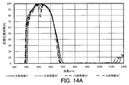
- FIG. 14A is a graph showing the normalized spectral transmittance of the optical filter according to Comparative Example 1 when the incident angles of light are 0 °, 30 °, 35 °, and 40 °.
- FIG. 14B is a graph showing the normalized spectral transmittance of the optical filter according to Comparative Example 1 when the incident angles of light are 45 °, 50 °, 55 °, 60 °, and 65 °.
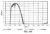
- FIG. 15A is a transmittance spectrum of the light-absorbing transparent substrate used for producing the optical filter according to Comparative Example 2 when the incident angle of light is 0 °.
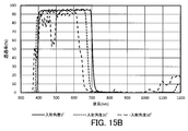
- FIG. 15B is a transmittance spectrum of the laminate according to Reference Example 4 when the incident angles of light are 0 °, 30 °, and 50 °.
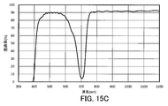
- FIG. 15C is a transmittance spectrum of the laminate according to Reference Example 5 when the incident angle of light is 0 °.
- FIG. 15A is a transmittance spectrum of the light-absorbing transparent substrate used for producing the optical filter according to Comparative Example 2 when the incident angle of light is 0 °.
- FIG. 15B is a transmittance spectrum of the laminate according to Reference Example 4 when the incident angles of light are 0 °, 30
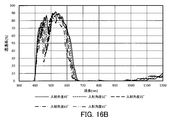
- FIG. 16A is a transmittance spectrum of the optical filter according to Comparative Example 2 when the incident angles of light are 0 °, 30 °, 35 °, and 40 °.
- FIG. 16B is a transmittance spectrum of the optical filter according to Comparative Example 2 when the incident angles of light are 45 °, 50 °, 55 °, 60 °, and 65 °.
- FIG. 17A is a graph showing the normalized spectral transmittance of the optical filter according to Comparative Example 2 when the incident angles of light are 0 °, 30 °, 35 °, and 40 °.
- FIG. 17B is a graph showing the normalized spectral transmittance of the optical filter according to Comparative Example 2 when the incident angles of light are 45 °, 50 °, 55 °, 60 °, and 65 °.
- the inventors of the present invention have devised an optical filter according to the present invention based on new findings obtained by the following study on an optical filter.
- an optical filter for blocking unnecessary light rays other than visible light rays is disposed.
- the use of optical filters with light absorbing layers to block unwanted light is being considered.
- an optical filter provided with a light absorbing layer often further includes a light reflecting layer formed of a dielectric multilayer film.
- the wavelength band of the light beam transmitted by the interference of the light beams reflected on the front and back surfaces of each layer and the wavelength band of the light beam to be reflected are determined.
- Light rays may enter the optical filter from various incident angles, but when the incident angle of light increases, the optical path length in each layer of the light reflection layer changes.
- the wavelength band of the transmitted light and the wavelength band of the reflected light shift to the short wavelength side. Therefore, when light of a predetermined wavelength band is reflected by the light reflection layer which is a dielectric multilayer film, the wavelength of the light beam to be shielded so that the transmittance characteristic of the optical filter does not greatly fluctuate depending on the incident angle of light. It is conceivable to define the boundary between the band and the wavelength band of the light beam to be transmitted by absorption of light.
- Patent Documents 1 and 2 evaluate the light transmission characteristics of the near infrared cut filter when the incident angles of light are 0 ° and 30 °. Moreover, in patent documents 3 and 4, the transmittance
- permeability spectrum of the infrared cut filter in case the incident angle of light is 0 degree, 25 degrees, and 35 degrees is evaluated.
- the optical filter even when the incident angle of light is large (for example, 40 ° or more), it is desirable that the change in the light transmission characteristic of the optical filter be small.
- the boundary between the wavelength band of the light beam transmitted by the dielectric multilayer film and the wavelength band of the light beam reflected is the wavelength band of the light beam transmitted by the light absorption layer and the wavelength band of the light beam absorbed
- the optical filter it is conceivable to design the optical filter to be located on the sufficiently long wavelength side of the boundary between In this case, even if the incident angle of light is increased, the boundary between the wavelength band of the light beam transmitted by the optical filter and the wavelength band of the light beam to be blocked can be suppressed from being shifted to the short wavelength side.
- ripple may occur when the incident angle of light is 40 ° or more.
- the sensitivity of the imaging device to a particular wavelength may be lower than that to other wavelengths, which may cause color unevenness in the obtained image.
- the present inventors can block unnecessary light rays and prevent occurrence of color unevenness in the image generated by the imaging device even when the incident angle of light is large.
- the present inventors have newly found that desired characteristics can be imparted to an optical filter by a predetermined light absorption layer without being combined with a light reflection layer constituted of a dielectric multilayer film, and the optical according to the present invention I devised a filter.
- spectral transmittance is transmittance when incident light of a specific wavelength is incident on an object such as a sample
- average transmittance is spectral transmittance within a predetermined wavelength range. It is the average value of the rate.
- transmittance spectrum is a spectrum in which the spectral transmittance at each wavelength within a predetermined wavelength range is arranged in order of wavelength.
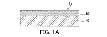
- the optical filter 1 a includes a light absorption layer 10.
- the light absorbing layer 10 contains a light absorbing agent, and the light absorbing agent absorbs at least part of light in the near infrared region.
- the following conditions (1) to (9) are satisfied.
- (1) The spectral transmittance at a wavelength of 380 nm is 20% or less.
- (2) The spectral transmittance at a wavelength of 450 nm is 75% or more.
- the average value of the spectral transmittance in the wavelength range of 500 to 600 nm is 80% or more.
- the spectral transmittance at a wavelength of 700 nm is 5% or less.
- the spectral transmittance at a wavelength of 715 nm is 3% or less.
- the average value of spectral transmittance in the wavelength range of 700 to 800 nm is 1% or less.
- the maximum value of the spectral transmittance in the wavelength range of 750 to 1080 nm is 1% or less.
- the maximum value of the spectral transmittance in the wavelength range of 1000 to 1100 nm is 2% or less.
- the wavelength band width of the wavelength band showing a spectral transmittance of 75% or more in the wavelength range of 400 to 700 nm is 170 nm or more.
- the sum of the wavelength bands of the plurality of wavelength bands is Define as "width”.
- the optical filter 1a is, ⁇ T S 0/40 380-530 ⁇ 3% , ⁇ T S 0/40 450-650 ⁇ 3%, and ⁇ T S 0/40 530-750 ⁇ 3% condition is satisfied.
- the above-mentioned normalized spectral transmittance normalizes the spectral transmittance at each of the above incident angles so that the maximum value of the wavelength range of 400 to 650 nm of the spectral transmittance at each of the above incident angles is 100%.
- the spectral transmittance is measured every 1 nm in the wavelength range of 300 to 1200 nm.
- normalized spectral transmittance is expressed as a percentage of the value obtained by dividing the spectral transmittance at each wavelength by the maximum value of the spectral transmittance in the wavelength range of 400 to 650 nm. Is determined.
- the optical filter 1a Since the optical filter 1a has the above-described characteristics, it is possible to appropriately block unnecessary light such as light in the near infrared region even without the light reflection layer formed of the dielectric multilayer film. In addition, light rays in the ultraviolet region can be appropriately shielded. Since the optical filter 1a does not include the light reflection layer formed of the dielectric multilayer film, no ripple occurs in the wavelength band of the light beam to be transmitted even if the incident angle of light is large, and imaging with the optical filter 1a Uneven color is less likely to occur in the image generated in the device. In addition, in the optical filter 1a, the boundary between the wavelength band of the light beam to be transmitted and the wavelength band of the light beam to be shielded is prevented from shifting to the short wavelength side as the incident angle of light increases.
- the optical filter 1a is, ⁇ T S 0/40 380-530 ⁇ 3% , ⁇ T S 0/40 450-650 ⁇ 3%, and since the ⁇ T S 0/40 530-750 ⁇ 3% condition is satisfied, the wavelength 380 to Shape of the normalized spectral transmittance curve at an incidence angle of 0 ° and the shape of a normalized spectral transmittance curve at an incidence angle of 40 ° in the range of 530 nm, wavelength 450 to 650 nm, and wavelength 530 to 750 nm The gap between is small.
- R (red), G (green), and B (blue) color filters for each pixel of an imaging device such as a CCD (Charge-Coupled Device) or a CMOS (Complementary Metal Oxide Semiconductor)
- RGB color filters for each pixel of an imaging device
- CCD Charge-Coupled Device
- CMOS Complementary Metal Oxide Semiconductor
- the optical filter 1a when “is placed”.
- the output from each pixel of the imaging device is appropriately adjusted by the optical filter 1a, and the spectral sensitivity characteristic corresponding to each pixel of the imaging device is likely to be well matched with the visual sensitivity.
- An optical filter for blocking unnecessary light rays is usually arranged in the vicinity of the imaging device so that its main surface is parallel to the light receiving surface of the imaging device.
- the incident angle at the optical filter of the light incident on the optical filter and further incident on the imaging device is substantially equal to the incident angle at the imaging device.
- the incident angle of the chief ray incident near the center of the imaging device is close to 0 °, and the incident angle of the chief ray incident on the peripheral portion of the imaging device is large. Therefore, when the shape of the spectral sensitivity curve changes depending on the incident angle of light in the imaging device, the hue in the image differs between the central portion and the peripheral portion of the image when the captured image is displayed or printed.
- the color of the subject that should be the same color in the image changes from the center to the periphery of the image, and is likely to be recognized as color unevenness.
- the shape of the spectral sensitivity curve changes in a narrow incident angle range of about 5 ° to 10 °
- the tint changes in the narrow range of the image, which is particularly likely to be recognized as color unevenness. If it is possible to suppress the change in shape of the normalized spectral transmittance curve due to the incident angle in the optical filter, it is possible to suppress the change in the shape of the spectral sensitivity curve due to the incident angle and color unevenness occurs in the image generated in the imaging device. It can prevent.
- the optical filter 1a desirably further satisfies the condition of ⁇ T S 0/40 650-1200 ⁇ 1%. In this case, even in the wavelength range of 650 to 1200 nm, the deviation between the shape of the normalized spectral transmittance curve at an incident angle of 0 ° and the shape of the normalized spectral transmittance curve at an incident angle of 40 ° is small.
- the optical filter 1a desirably further satisfies the condition of ⁇ T S 0/40 380-1200 ⁇ 1.5%.
- the difference between the shape of the normalized spectral transmittance curve at an incident angle of 0 ° and the shape of the normalized spectral transmittance curve at an incident angle of 40 ° is small over a wavelength range of 380 to 1200 nm.
- the wavelength range of 380 to 530 nm is a wavelength for specifying the sensitivity characteristic of the pixel corresponding to the B (blue) filter among the RGB color filters incorporated in the imaging device or arranged in the vicinity of the imaging device It corresponds to the range of.
- the wavelength range of 450 to 650 nm is a wavelength for specifying the sensitivity characteristic of the pixel corresponding to the G (green) filter among the RGB color filters incorporated in the imaging device or arranged in the vicinity of the imaging device It corresponds to the range of.
- a wavelength range of 530 to 750 nm is a wavelength for specifying the sensitivity characteristic of the pixel corresponding to the R (red) filter among the RGB color filters incorporated in the imaging device or arranged in the vicinity of the imaging device It corresponds to the range of.
- the wavelength range of 650 to 1200 nm corresponds to the range of the near infrared wavelength to be shielded.
- the wavelength range of 380 to 1200 nm includes the wavelength range described above, and corresponds to the wavelength range for specifying the brightness of light taken in by the camera module or the imaging device through the optical filter.
- the optical filter 1a is desirably, ⁇ T S 0/50 380-530 ⁇ 4% , ⁇ T S 0/50 450-650 ⁇ 4%, ⁇ T S 0/50 530-750 ⁇ 4%, ⁇ T S 0/50 650
- the conditions of ⁇ 1200 ⁇ 1.5% and ⁇ T S 0/50 380-1200 ⁇ 2% are further satisfied.
- the difference between the shape of the normalized spectral transmittance curve at an incident angle of 0 ° and the shape of the normalized spectral transmittance curve at an incident angle of 50 ° is small.
- it is easy to prevent the occurrence of color unevenness in the image generated in the imaging device.
- the optical filter 1a is desirably, ⁇ T S 0/60 380-530 ⁇ 4.5% , ⁇ T S 0/60 450-650 ⁇ 4.5%, ⁇ T S 0/60 530-750 ⁇ 4.5%, The conditions of ⁇ T S 0/60 650-1200 ⁇ 1.5% and ⁇ T S 0/60 380-1200 ⁇ 2.5% are further satisfied.
- the difference between the shape of the normalized spectral transmittance curve at an incident angle of 0 ° and the shape of the normalized spectral transmittance curve at an incident angle of 60 ° is small. Thus, even when light is incident on the optical filter 1a at an incident angle of 60 ° in the imaging device, it is easy to prevent the occurrence of color unevenness in the image generated in the imaging device.
- the optical filter 1a is desirably, ⁇ T S 0/65 380-530 ⁇ 5% , ⁇ T S 0/65 450-650 ⁇ 5%, ⁇ T S 0/65 530-750 ⁇ 5%, ⁇ T S 0/65 650
- the conditions of ⁇ 1200 ⁇ 1.5% and ⁇ T S 0/65 380-1200 ⁇ 3% are further satisfied.
- the difference between the shape of the normalized spectral transmittance curve at an incident angle of 0 ° and the shape of the normalized spectral transmittance curve at an incident angle of 65 ° is small.
- the optical filter 1a even when light is incident on the optical filter 1a at an incident angle of 65 ° in the imaging device, it is easy to prevent occurrence of color unevenness in the image generated in the imaging device.
- an imaging apparatus capable of imaging using a wide angle lens having a large angle of view is provided with the optical filter 1a, it is easy to prevent occurrence of color unevenness in an image photographed using such a wide angle lens.
- the light rays incident on the cover glass positioned in front of the lens necessarily include light incident at a large incident angle. If the above conditions are satisfied in the optical filter 1a, even if the optical filter 1a is used as a cover glass in the imaging device, color unevenness hardly occurs in the image generated in the imaging device. In addition, if the optical filter 1a also functions as a cover glass, the number of parts of the imaging device can be reduced, and the height of the imaging device can be easily reduced. In addition, the degree of freedom in lens design also increases. Furthermore, it is also possible to prevent flare or ghosting caused by reflection on the main surface of the conventional optical filter disposed separately from the cover glass.
- the optical filter 1a is desirably, ⁇ T S 30/40 380-530 ⁇ 3% , ⁇ T S 30/40 450-650 ⁇ 3%, ⁇ T S 30/40 530-750 ⁇ 3%, ⁇ T S 30/40 650 -1200 ⁇ 1%, and further satisfy ⁇ T S 30/40 380-1200 ⁇ 1.5% conditions.
- the difference between the shape of the normalized spectral transmittance curve at an incident angle of 30 ° and the shape of the normalized spectral transmittance curve at an incident angle of 40 ° is small.
- the optical filter 1a is desirably, ⁇ T S 30/50 380-530 ⁇ 3% , ⁇ T S 30/50 450-650 ⁇ 3%, ⁇ T S 30/50 530-750 ⁇ 3%, ⁇ T S 30/50 650 -1200 ⁇ 1%, and further satisfy ⁇ T S 30/50 380-1200 ⁇ 1.5% conditions.
- the difference between the shape of the normalized spectral transmittance curve at an incident angle of 30 ° and the shape of the normalized spectral transmittance curve at an incident angle of 50 ° is small.
- the optical filter 1a is desirably, ⁇ T S 30/60 380-530 ⁇ 4% , ⁇ T S 30/60 450-650 ⁇ 4%, ⁇ T S 30/60 530-750 ⁇ 4%, ⁇ T S 30/60 650 -1200 ⁇ 1.5%, and further satisfy ⁇ T S 30/60 380-1200 ⁇ 2% conditions.
- the difference between the shape of the normalized spectral transmittance curve at an incident angle of 30 ° and the shape of the normalized spectral transmittance curve at an incident angle of 60 ° is small.
- the optical filter 1a is desirably, ⁇ T S 30/65 380-530 ⁇ 4.5% , ⁇ T S 30/65 450-650 ⁇ 4.5%, ⁇ T S 30/65 530-750 ⁇ 4.5%, The conditions of ⁇ T S 30/65 650-1200 ⁇ 1.5% and ⁇ T S 30/65 380-1200 ⁇ 2.5% are further satisfied. In this case, the difference between the shape of the normalized spectral transmittance curve at an incident angle of 30 ° and the shape of the normalized spectral transmittance curve at an incident angle of 65 ° is small.
- the value of ⁇ T S 0 / y WV in the optical filter 1a desirably satisfies the condition shown in Table 1.
- the value of ⁇ T S 30 / y WV in the optical filter 1a desirably satisfies the conditions shown in Table 2.
- the light absorbing agent contained in the light absorbing layer 10 absorbs at least a part of light in the near infrared region, and the above conditions (1) to (9) in the optical filter 1 a and ⁇ T S 0/40 380 -530 ⁇ 3%, ⁇ T S 0/40 450-650 ⁇ 3%, and [Delta] T S 0/40 and 530-750 ⁇ 3% conditions are not particularly limited as long as it is filled.
- the light absorber is formed of, for example, phosphonic acid and copper ions.
- the light absorption layer 10 can absorb light in a near infrared region and a wide wavelength band of a visible region adjacent to the near infrared region. Therefore, even if the optical filter 1a does not include the light reflection layer, it is possible to exhibit desired characteristics.
- the phosphonic acid contains, for example, a first phosphonic acid having an aryl group.
- the aryl group is attached to the phosphorus atom.
- the aryl group which the first phosphonic acid has is, for example, a phenyl group, a benzyl group, a toluyl group, a nitrophenyl group, a hydroxyphenyl group, a halogenated phenyl group in which at least one hydrogen atom in the phenyl group is substituted by a halogen atom, Alternatively, it is a halogenated benzyl group in which at least one hydrogen atom in the benzene ring of the benzyl group is substituted by a halogen atom.
- the phosphonic acid desirably further comprises a second phosphonic acid having an alkyl group.
- the alkyl group is attached to the phosphorus atom.
- the alkyl group possessed by the second phosphonic acid is, for example, an alkyl group having 6 or less carbon atoms.
- the alkyl group may have either linear or branched chain.
- the light absorbing layer 10 When the light absorbing layer 10 includes a light absorbing agent formed of phosphonic acid and copper ions, the light absorbing layer 10 further includes, for example, a phosphate ester in which the light absorbing agent is dispersed, and a matrix resin. The light absorption layer 10 further contains, as necessary, a hydrolysis-condensation product of an alkoxysilane monomer.
- the phosphate ester contained in the light absorption layer 10 is not particularly limited as long as the light absorber can be appropriately dispersed, but for example, a phosphate diester represented by the following formula (c1) and a table by the following formula (c2) And / or at least one of the following phosphoric monoesters.
- R 21 , R 22 and R 3 are each a monovalent functional group represented by — (CH 2 CH 2 O) n R 4 and n Is an integer of 1 to 25 and R 4 is an alkyl group having 6 to 25 carbon atoms.
- R 21 , R 22 and R 3 are functional groups of the same or different type from one another.
- the phosphoric acid ester is not particularly limited.
- Plysurf A208N polyoxyethylene alkyl (C12, C13) ether phosphoric acid ester
- Plysurf A208 F polyoxyethylene alkyl (C8) ether phosphoric acid ester
- Plysurf A208 B Polyoxyethylene lauryl ether phosphate
- Plysurf A 219 B Polyoxyethylene lauryl ether phosphate
- Plysurf AL Polyoxyethylene styrenated phenyl ether phosphate
- Plysurf A 212 C Polyoxyethylene tridecyl ether phosphate
- Plysurf A 215 C polyoxyethylene tridecyl ether phosphate ester.
- NIKKOL DDP-2 polyoxyethylene alkyl ether phosphate
- NIKKOL DDP-4 polyoxyethylene alkyl ether phosphate
- NIKKOL DDP-6 polyoxyethylene alkyl ether phosphate possible.
- the matrix resin contained in the light absorbing layer 10 is, for example, a resin capable of dispersing a light absorbing agent and capable of being thermally cured or ultraviolet curable. Furthermore, when a resin layer of 0.1 mm is formed of the resin as a matrix resin, the transmittance of the resin layer to light with a wavelength of 350 to 900 nm is, for example, 80% or more, preferably 85% or more, More preferably, resin of 90% or more can be used, but in the optical filter 1a, the conditions of the above (1) to (9), ⁇ T S 0/40 380-530 ⁇ 3%, ⁇ T S 0/40 450
- the matrix resin is not limited to a specific resin as long as the conditions of ⁇ 650 ⁇ 3% and ⁇ T S 0/40 530 ⁇ 750 ⁇ 3% are satisfied.
- the content of phosphonic acid in the light absorption layer 10 is, for example, 3 to 180 parts by mass with respect to 100 parts by mass of the matrix resin.
- the matrix resin contained in the light absorption layer 10 is, for example, (poly) olefin resin, polyimide resin, polyvinyl butyral resin, polycarbonate resin, polyamide resin, polysulfone resin, polyether sulfone resin, polyamide imide resin, (modified) acrylic resin, It is an epoxy resin or a silicone resin.
- the matrix resin may contain an aryl group such as a phenyl group, and is preferably a silicone resin containing an aryl group such as a phenyl group.
- the matrix resin is a silicone resin containing an aryl group
- the light absorption layer 10 tends to have good crack resistance.
- the matrix resin of the light absorbing layer 10 is a silicone resin containing an aryl group
- the phosphoric acid ester contained in the light absorbing layer 10 may be a phosphoric acid ester represented by Formula (c1) or Formula (c2) It is desirable to have a flexible linear organic functional group such as an oxyalkyl group.
- silicone resin used as a matrix resin include KR-255, KR-300, KR-2621-1, KR-211, KR-311, KR-216, KR-212, KR-251, and KR. -5230 can be mentioned. All of these are silicone resins manufactured by Shin-Etsu Chemical Co., Ltd.
- the hydrolysis condensation polymerization product of the alkoxysilane monomer which may be contained in the optical filter 1a is, for example, the hydrolysis condensation polymerization product of the following alkoxysilane monomer.
- the alkoxysilane monomers are tetramethoxysilane, tetraethoxysilane, methyltrimethoxysilane, methyltriethoxysilane, dimethyldiethoxysilane, dimethyldimethoxysilane, phenyltrimethoxysilane, phenyltriethoxysilane, 3-glycidoxypropyltriol. Methoxysilane, 3-glycidoxypropyltriethoxysilane, or 3-glycidoxypropylmethyldiethoxysilane.
- the optical filter 1a further includes, for example, a transparent dielectric substrate 20.
- a transparent dielectric substrate 20 One main surface of the transparent dielectric substrate 20 is covered with the light absorption layer 10.
- Properties of the transparent dielectric substrate 20 is an optical filter 1a, a condition of the (1) ⁇ (9), ⁇ T S 0/40 380-530 ⁇ 3%, ⁇ T S 0/40 450-650 ⁇ 3% And ⁇ T S 0/40 530-750 ⁇ 3% conditions are not particularly limited.
- the transparent dielectric substrate 20 is, for example, a dielectric substrate having a high average transmittance (eg, 80% or more, preferably 85% or more, more preferably 90% or more) at 450 to 600 nm.
- the transparent dielectric substrate 20 is made of, for example, glass or resin.
- the glass contains, for example, borosilicate glass such as D263 T eco, soda lime glass (blue plate), white sheet glass such as B270, alkali-free glass, or copper.
- Infrared absorbing glass such as phosphate glass or fluorophosphate glass containing copper.
- the transparent dielectric substrate 20 is an infrared absorbing glass such as copper containing phosphate glass or copper containing fluorophosphate glass, the infrared absorption performance and light of the transparent dielectric substrate 20
- the combination with the infrared absorption performance of the absorption layer 10 can provide the optical filter 1a with a desired infrared absorption performance.
- Such infrared absorbing glass is, for example, BG-60, BG-61, BG-62, BG-63, or BG-67 manufactured by SCHOTT, 500EXL manufactured by Nippon Electric Glass Co., Ltd., or Hoya Company CM5000, CM500, C5000, or C500S.
- the transparent dielectric substrate 20 may have an ultraviolet absorbing property.
- the transparent dielectric substrate 20 may be a crystalline substrate having transparency, such as magnesium oxide, sapphire, or quartz.
- sapphire is hard to scratch because of its high hardness.
- plate-shaped sapphire is disposed on the front surface of a camera module or lens provided in a portable terminal such as a smartphone and a mobile phone as a scratch-resistant protective material such as a protective filter or a cover glass in an imaging device.
- a portable terminal such as a smartphone and a mobile phone
- a scratch-resistant protective material such as a protective filter or a cover glass in an imaging device.
- the resin is, for example, (poly) olefin resin, polyimide resin, polyvinyl butyral resin, polycarbonate resin, polyamide resin, polysulfone resin, polyether sulfone resin, polyamide imide resin, (Modified) Acrylic resin, epoxy resin, or silicone resin.
- the optical filter 1a can be manufactured, for example, by applying a coating solution for forming the light absorption layer 10 on one main surface of the transparent dielectric substrate 20 to form a coating, and drying the coating.
- the method of preparing the coating solution and the method of manufacturing the optical filter 1a will be described by taking, as an example, the case where the light absorbing layer 10 contains a light absorbing agent formed of phosphonic acid and copper ions.
- a copper salt such as copper acetate monohydrate is added to a predetermined solvent such as tetrahydrofuran (THF) and stirred to obtain a solution of copper salt.
- a phosphate diester represented by the formula (c1) or a phosphate ester compound such as a phosphate monoester represented by the formula (c2) is added to the copper salt solution and stirred to prepare a solution A.
- the first phosphonic acid is added to a predetermined solvent such as THF and stirred to prepare a solution B.
- the solution B contains a plurality of types of first phosphonic acids
- a predetermined solvent such as THF may be added to each type of phosphonic acid, and a plurality of solutions prepared in advance may be mixed to prepare the solution B.
- the optical filter 1a contains a hydrolytic condensation polymer of an alkoxysilane monomer, for example, an alkoxysilane monomer is further added to prepare a solution B.
- solution B is added to solution A and stirred for a predetermined time.
- a predetermined solvent such as toluene is added to the solution and stirred to obtain a solution C.
- a desolvation process is performed for a predetermined time while heating the solution C to obtain the solution D.
- a solvent such as THF and a component generated by dissociation of a copper salt such as acetic acid (boiling point: about 118 ° C.) are removed, and a light absorbing agent is generated by the first phosphonic acid and the copper ion.
- the temperature for heating solution C is determined based on the boiling point of the component to be removed which has been dissociated from the copper salt.
- a solvent such as toluene (boiling point: about 110 ° C.) used to obtain the liquid C also evaporates. Since it is desirable that the solvent remains to some extent in the coating solution, it is preferable from this viewpoint that the amount of the solvent added and the time for the desolvation treatment be defined.
- o-xylene (boiling point: about 144 ° C.) can be used instead of toluene. In this case, since the boiling point of o-xylene is higher than the boiling point of toluene, the amount of addition can be reduced to about one fourth of the amount of addition of toluene.
- a matrix resin such as silicone resin is added to solution D and stirred to prepare a coating solution.
- the coating solution is applied to one of the main surfaces of the transparent dielectric substrate 20 to form a coating.
- the coating liquid is applied to one main surface of the transparent dielectric substrate 20 by die coating, spin coating, or application by a dispenser to form a coating.
- this coating film is subjected to a predetermined heat treatment to cure the coating film.
- the coating is exposed to an environment at a temperature of 50 ° C. to 200 ° C. for a predetermined time.
- the coating solution may further contain a secondary phosphonic acid.
- the coating liquid can be prepared by mixing and stirring the liquid D, the liquid H containing the second phosphonic acid, and the matrix resin.
- Solution H can be prepared, for example, as follows.
- a copper salt such as copper acetate monohydrate is added to a predetermined solvent such as tetrahydrofuran (THF) and stirred to obtain a solution of copper salt.
- a phosphate diester represented by the formula (c1) or a phosphate ester compound such as a phosphate monoester represented by the formula (c2) is added to the solution of the copper salt and stirred to prepare a solution E. Do.
- secondary phosphonic acid is added to a predetermined solvent such as THF and stirred to prepare solution F.
- the solution F is added to the solution E and stirred for a predetermined time.
- a predetermined solvent such as toluene is added to this solution and stirred to obtain solution G.
- the solvent removal treatment is performed for a predetermined time while heating the solution G to obtain the solution H.
- the light absorption layer 10 may be formed as a single layer or may be formed as a plurality of layers.
- the light absorbing layer 10 may be, for example, a first layer containing a light absorbing agent formed of a first phosphonic acid and a copper ion, and a second layer It has a second layer containing a light absorber formed by phosphonic acid and copper ions.
- the coating solution for forming the first layer is obtained by adding a matrix resin such as a silicone resin to solution D and stirring.
- the second layer is formed using a coating solution prepared separately from the coating solution for forming the first layer.
- the coating liquid for forming the second layer is obtained, for example, by adding a matrix resin such as a silicone resin to solution H and stirring.
- a coating solution for forming the first layer and a coating solution for forming the second layer are applied to form a coating, and the coating is subjected to a predetermined heat treatment to cure the coating.
- the first layer and the second layer can be formed.
- the coating is exposed to an environment at a temperature of 50 ° C. to 200 ° C. for a predetermined time.
- the order in which the first layer and the second layer are formed is not particularly limited, and the first layer and the second layer may be formed in different periods or may be formed in the same period.
- a protective layer may be formed between the first layer and the second layer.
- the protective layer is formed of, for example, a vapor deposited film of SiO 2 .
- the optical filter 1a can be changed from various viewpoints.
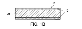
- the optical filter 1a may be changed to each of the optical filters 1b to 1e shown in FIGS. 1B to 1E.
- the optical filters 1b to 1e are configured in the same manner as the optical filter 1a, unless otherwise specified.
- the components of the optical filters 1b to 1e which are the same as or correspond to the components of the optical filter 1a are designated by the same reference numerals, and the detailed description thereof is omitted.
- the description on the optical filter 1a also applies to the optical filters 1b to 1e unless there is a technical contradiction.
- the light absorption layer 10 is formed on both main surfaces of the transparent dielectric substrate 20. Accordingly, the conditions shown in the above (1) to (9) are not obtained by one light absorbing layer 10 but by two light absorbing layers 10 separated by the transparent dielectric substrate 20, and ⁇ T S 0/40 380 -530 ⁇ 3%, ⁇ T S 0/40 450-650 ⁇ 3%, and ⁇ T S 0/40 530-750 ⁇ 3% of conditions are met.
- the thickness of the light absorption layer 10 on both main surfaces of the transparent dielectric substrate 20 may be the same or different.
- the light absorbing layer is formed on both main surfaces of the transparent dielectric substrate 20 so that the thickness of the light absorbing layer 10 necessary for the optical filter 1b to obtain the desired optical characteristics may be evenly or unevenly distributed. 10 are formed. Thereby, the thickness of each light absorption layer 10 formed on one main surface of the transparent dielectric substrate 20 of the optical filter 1b is smaller than that of the optical filter 1a. By forming the light absorption layer 10 on both main surfaces of the transparent dielectric substrate 20, warping of the optical filter 1b is suppressed even when the transparent dielectric substrate 20 is thin.
- Each of the two light absorption layers 10 may be formed as a plurality of layers.
- the light absorption layer 10 is formed on both main surfaces of the transparent dielectric substrate 20.
- the optical filter 1 c includes the anti-reflection film 30.
- the antireflective film 30 is a film formed to form an interface between the optical filter 1c and air, for reducing reflection of light in the visible region.
- the antireflective film 30 is a film formed of, for example, a resin, an oxide, and a dielectric such as a fluoride.
- the antireflective film 30 may be a multilayer film formed by laminating two or more types of dielectrics having different refractive indexes.
- the antireflective film 30 may be a dielectric multilayer film made of a low refractive index material such as SiO 2 and a high refractive index material such as TiO 2 or Ta 2 O 5 . In this case, Fresnel reflection at the interface between the optical filter 1c and the air is reduced, and the amount of light in the visible region transmitted through the optical filter 1c can be increased.
- the anti-reflection film 30 may be formed on both sides of the optical filter 1c, or may be formed on one side of the optical filter 1c.
- the optical filter 1 d is constituted only by the light absorption layer 10.
- the optical filter 1d is formed by applying a coating liquid to a predetermined substrate such as a glass substrate, a resin substrate, a metal substrate (for example, a steel substrate or a stainless steel substrate) to form a coating and curing the coating. It can be manufactured by peeling from a substrate.
- the optical filter 1d may be manufactured by a casting method.
- the optical filter 1 d is thin because it does not include the transparent dielectric substrate 20. Therefore, the optical filter 1d can contribute to reducing the height of the imaging device.
- the optical filter 1 e includes a light absorption layer 10 and a pair of anti-reflection films 30 disposed on both sides thereof.
- the optical filter 1e can contribute to reducing the height of the imaging device, and can increase the amount of light in the visible region as compared to the optical filter 1d.
- Each of the optical filters 1a to 1e may be changed to include an infrared absorption layer (not shown) separately from the light absorption layer 10, as necessary.
- the infrared absorbing layer contains, for example, an organic infrared absorber such as a cyanine type, phthalocyanine type, squarylium type, diimmonium type, or azo type, or an infrared absorber made of a metal complex.
- the infrared absorption layer contains, for example, one or more infrared absorbers selected from these infrared absorbers. This organic infrared absorber has a small wavelength range (absorption band) of absorbable light and is suitable for absorbing light in a specific range of wavelengths.
- Each of the optical filters 1a to 1e may be changed to include an ultraviolet absorbing layer (not shown) separately from the light absorbing layer 10, as necessary.
- the ultraviolet absorbing layer contains, for example, ultraviolet absorbers such as benzophenone type, triazine type, indole type, merocyanine type, and oxazole type.
- the ultraviolet absorbing layer contains, for example, one or more ultraviolet absorbers selected from these ultraviolet absorbers. These UV absorbers may be included, for example, those that absorb UV light at around 300 to 340 nm, emit light (fluorescence) longer than the wavelength absorbed, and function as a fluorescent agent or a brightening agent.
- the ultraviolet absorbing layer can reduce the incidence of ultraviolet light that causes deterioration of the material used for the optical filter such as resin.
- the above-mentioned infrared ray absorbing agent and / or ultraviolet ray absorbing agent may be previously contained in a transparent dielectric substrate 20 made of resin to form a substrate having a property of absorbing infrared rays and / or ultraviolet rays.
- the resin needs to be able to appropriately dissolve or disperse the infrared absorber and / or the ultraviolet absorber and be transparent.
- Such resins include (poly) olefin resins, polyimide resins, polyvinyl butyral resins, polycarbonate resins, polyamide resins, polysulfone resins, polyether sulfone resins, polyamideimide resins, (modified) acrylic resins, epoxy resins, and silicone resins Can be illustrated.
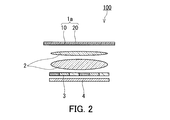
- the optical filter 1 a is used, for example, to manufacture an imaging device 100 (camera module).
- the imaging device 100 includes a lens system 2, an imaging element 4, and an optical filter 1a.
- the imaging device 100 further includes, for example, a color filter 3 disposed in front of the imaging element 4 and having three color filters of R (red), G (green), and B (blue). .
- the optical filter 1 a is disposed in front of the color filter 3.
- the color filter 3 and the imaging device 4 receive the light having passed through the lens system 2.
- the light absorption layer 10 is formed in contact with the surface of the transparent dielectric substrate 20 close to the lens system 2.
- a high hardness material such as sapphire for the transparent dielectric substrate 20
- the effect of protecting the lens system 2 or the imaging device 4 is enhanced.
- the color filter 3 filters of three colors of R (red), G (green), and B (blue) are arranged in a matrix, and R (red) right above each pixel of the imaging device 4, A filter of any of G (green) and B (blue) is disposed.
- the image sensor 4 receives light from an object that has passed through the lens system 2, the optical filter 1 a, and the color filter 3.
- the imaging device 100 generates an image based on the information related to the charge generated by the light received by the imaging device 4.
- the color image sensor may be configured by integrating the color filter 3 and the imaging device 4.
- the imaging device 100 may be modified such that the optical filter 1 a is disposed close to the color filter 3.
- the imaging device 100 may be modified to include at least one of the optical filters 1b to 1e instead of the optical filter 1a or together with the optical filter 1a.
- ⁇ Transmittance spectrum measurement> Transmittance spectrum when light having a wavelength of 300 to 1200 nm is incident on the optical filters according to the examples and comparative examples, the semifinished products of the optical filters according to some examples and comparative examples, or the laminate according to the reference example And UV-visible spectrophotometer (manufactured by JASCO, product name: V-670).
- the incident angle of incident light was set to at least one of 0 °, 30 °, 35 °, 40 °, 45 °, 50 °, 55 °, 60 °, and 65 °.
- a rate curve normalized spectral transmittance curve
- the wavelength Wnm to Vnm of the absolute value of the difference between the normalized spectral transmittance at the incident angle of x ° and the normalized spectral transmittance at the incident angle of y ° was calculated.
- Example 1 1.125 g of copper acetate monohydrate ((CH 3 COO) 2 Cu ⁇ H 2 O) and 60 g of tetrahydrofuran (THF) were mixed and stirred for 3 hours to obtain a copper acetate solution. Next, 0.412 g of Plysurf A 208 N (manufactured by Dai-ichi Kogyo Seiyaku Co., Ltd.), which is a phosphoric acid ester compound, was added to the obtained copper acetate solution, and the mixture was stirred for 30 minutes to obtain a solution A.
- Plysurf A 208 N manufactured by Dai-ichi Kogyo Seiyaku Co., Ltd.
- the B1-1 liquid and the B1-2 liquid are mixed and stirred for 1 minute, and 2.166 g of methyltriethoxysilane (MTES: CH 3 Si (OC 2 H 5 ) 3 ) (manufactured by Shin-Etsu Chemical Co., Ltd.) 0.710 g of tetraethoxysilane (TEOS: Si (OC 2 H 5 ) 4 ) (special grade manufactured by Kishida Chemical Co., Ltd.) was added, and the mixture was further stirred for 1 minute to obtain a solution B1.
- Solution B was added to solution A while stirring solution A, and the solution was stirred at room temperature for 1 minute.
- Solution C1 was placed in a flask and desolvated by a rotary evaporator (manufactured by Tokyo Rika Kikai, model: N-1110SF) while heating with an oil bath (manufactured by Tokyo Rika Kikai, model: OSB-2100) .
- the set temperature of the oil bath was adjusted to 105 ° C. Thereafter, the solution after the solvent removal treatment was taken out of the flask to obtain a solution D1.
- Liquid D1 was a dispersion of fine particles of phenyl-based copper phosphonate (light absorber) containing copper phenylphosphonate and copper 4-bromophenylphosphonate.
- the D1 solution was transparent, and the fine particles of the light absorbing agent were well dispersed in the D1 solution.
- Example using a dispenser in the range of 30 mm ⁇ 30 mm at the center of both sides of a transparent glass substrate made of borosilicate glass having dimensions of 76 mm ⁇ 76 mm ⁇ 0.07 mm
- the light absorbing composition according to 1 was applied to form a coating.
- a frame having an opening corresponding to the application range of the coating solution was placed on the transparent glass substrate to stop the coating solution so that the coating solution did not flow out when the light absorbing composition was applied to the transparent glass substrate.
- the application amount of the light absorbing composition was determined so that the total thickness of the layers derived from the coating of the light absorbing composition on both sides of the transparent glass substrate finally becomes about 180 ⁇ m.
- the transparent glass substrate having a coating of the undried light absorbing composition was placed in an oven, and heat treatment was performed at 85 ° C. for 6 hours to cure the coating.
- the transparent glass substrate on which the above-mentioned coating film was formed was placed in a constant temperature and humidity chamber set to a temperature of 85 ° C. and a relative humidity of 85% for 20 hours to perform a humidification treatment.
- the humidification treatment was performed to promote hydrolysis and condensation polymerization of the alkoxysilane monomer contained in the light absorbing composition applied on the transparent glass substrate to form a hard and dense matrix in the light absorbing layer. Then, the area
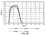
- the characteristic values read from the transmittance spectrum of the optical filter according to Example 1 at an incident angle of 0 ° are shown in Table 3. Normalized spectral transmittance curves of the optical filter according to Example 1 at incident angles of 0 °, 30 °, 35 °, 40 °, 45 °, 50 °, 55 °, 60 °, and 65 ° are shown in FIG. 4A and FIG. Shown in 4B.
- the value of ⁇ T S 0 / y WV when the incident angle x ° is 0 °
- the value of ⁇ T S 30 / y WV when the incident angle x ° is 30 °. It shows in Table 4 and Table 5.
- the optical filter according to Example 1 has the characteristics of being able to satisfactorily block light in the ultraviolet region and the near infrared region, and to sufficiently transmit light in the visible region.
- the normalized spectral transmittance in the region of wavelength 380 nm or less and the region of wavelength 700 nm or more with respect to the incident angle of 0 ° to 65 ° is sufficiently low.
- the normalized spectral transmittance at 450 nm and at a wavelength of 500 to 600 nm was sufficiently high.
- the optical filter according to the first embodiment has an ultraviolet range and a near infrared range even when sensitivity correction is performed so as to compensate for the decrease in light amount according to the incident angle to the imaging device assumed in design in the imaging device. It had advantageous characteristics in order to sufficiently transmit light in the visible region while shielding light well. Further, in the optical filter according to the first embodiment, the deviation of the shape of the normalized spectral transmittance curve at each incident angle is small, and color unevenness occurs in the image generated by the imaging device using the optical filter according to the first embodiment. It is thought that it is hard to occur.
- Example 2 1.125 g of copper acetate monohydrate ((CH 3 COO) 2 Cu ⁇ H 2 O) and 60 g of tetrahydrofuran (THF) were mixed and stirred for 3 hours to obtain a copper acetate solution. Next, 0.412 g of Plysurf A 208 N (manufactured by Dai-ichi Kogyo Seiyaku Co., Ltd.), which is a phosphoric acid ester compound, was added to the obtained copper acetate solution, and the mixture was stirred for 30 minutes to obtain a solution A.
- Plysurf A 208 N manufactured by Dai-ichi Kogyo Seiyaku Co., Ltd.
- the B2-1 solution and the B2-2 solution are mixed and stirred for 1 minute, and 1.943 g of methyltriethoxysilane (MTES: CH 3 Si (OC 2 H 5 ) 3 ) (manufactured by Shin-Etsu Chemical Co., Ltd.) A tetraethoxysilane (TEOS: Si (OC 2 H 5 ) 4 ) (special grade by Kishida Chemical Co., Ltd.) 0.634 g was added, and the mixture was further stirred for 1 minute to obtain a solution B2.
- Solution B was added to solution A while stirring solution A, and the solution was stirred at room temperature for 1 minute.
- Solution C2 is placed in a flask and desolvated by a rotary evaporator (manufactured by Tokyo Rika Kikai, model: N-1110SF) while warming with an oil bath (manufactured by Tokyo Rika Kikai, model: OSB-2100) The The set temperature of the oil bath was adjusted to 105 ° C. Thereafter, the solution after desolvation was taken out of the flask to obtain a D2 solution.
- Liquid D2 was a dispersion of fine particles of phenyl-based copper phosphonate (light absorber) containing copper phenylphosphonate and copper 4-bromophenylphosphonate.
- the D2 solution was transparent, and the fine particles were well dispersed in the D2 solution.
- the solvent G was removed by a rotary evaporator while the solution G2 was placed in a flask and warmed with an oil bath. The set temperature of the oil bath was adjusted to 105 ° C. Thereafter, the solution after the desolvation treatment was taken out of the flask to obtain an H2 solution.
- the H2 solution was a dispersion of copper butylphosphonate fine particles. The H2 solution was transparent, and the fine particles were well dispersed in the H2 solution.
- a dispenser is used in the range of 30 mm ⁇ 30 mm at the center of one main surface of a transparent glass substrate (SCHOTT's product name: D263 T eco) made of borosilicate glass having dimensions of 76 mm ⁇ 76 mm ⁇ 0.21 mm
- the light absorbing composition according to Example 2 was applied to form a coating.
- a frame having an opening corresponding to the application range of the coating solution was placed on the transparent glass substrate to stop the coating solution so that the coating solution did not flow out when the light absorbing composition was applied to the transparent glass substrate.
- the application amount of the light absorbing composition was determined such that the thickness of the layer derived from the coating of the light absorbing composition finally became about 170 ⁇ m.
- the transparent glass substrate having a coating of the undried light absorbing composition was placed in an oven, and heat treatment was performed at 85 ° C. for 6 hours to cure the coating. Thereafter, the transparent glass substrate on which the above-mentioned coating film is formed is placed in a constant temperature and humidity chamber set to a temperature of 85 ° C. and a relative humidity of 85% for 20 hours to perform humidification treatment, and a light absorbing layer is formed on the transparent glass substrate.
- An optical filter according to Example 2 was obtained.
- the humidification treatment was performed to promote hydrolysis and condensation polymerization of the alkoxysilane monomer contained in the light absorbing composition applied on the transparent glass substrate to form a hard and dense matrix in the light absorbing layer.
- the thickness of the light absorption layer of the optical filter according to Example 2 was 170 ⁇ m.
- Transmittance spectra of the optical filter according to Example 2 at incident angles of 0 °, 30 °, 35 °, 40 °, 45 °, 50 °, 55 °, 60 °, and 65 ° are shown in FIGS. 5A and 5B.
- the characteristic values read from the transmittance spectrum of the optical filter according to Example 2 at an incident angle of 0 ° are shown in Table 6.
- Normalized spectral transmittance curves of the optical filter according to Example 2 at incident angles of 0 °, 30 °, 35 °, 40 °, 45 °, 50 °, 55 °, 60 °, and 65 ° are shown in FIG. 6A and FIG. Shown in 6B.
- the transmission band extends to the short wavelength side as compared with the optical filter according to the first embodiment, and the transmittance of 20% is weak at a wavelength of 380 nm. Indicated.
- the short wavelength limit of the wavelength range of an electromagnetic wave corresponding to visible light is described as 360 to 400 nm.
- the transmittance rapidly increases with the increase of the wavelength near the short wavelength limit of visible light.
- a general imaging element has low sensitivity in this band. Therefore, it is considered that there is no practical problem in incorporating the optical filter according to the second embodiment into the imaging device.
- the transmittance in the region of wavelengths less than 380 nm and in the region of wavelengths of 700 nm or more is sufficiently low except in the region of wavelengths of 1100 nm or more, and the transmittance at wavelengths of 450 nm and 500 to 600 nm is sufficient. high.
- the optical filter according to the second embodiment has a characteristic that it can well block light in the ultraviolet region and the near infrared region, and can sufficiently transmit light in the visible region. As shown in FIGS.
- the normalized spectral transmittance in the region of wavelength less than 380 nm and in the region of wavelength 700 nm or more with respect to the incident angle of 0 ° to 65 ° is 1100 nm or more.
- the region was low enough that the normalized spectral transmittance at wavelengths 450 nm and 500-600 nm was sufficiently high.
- the optical filter according to the second embodiment has an ultraviolet range and a near infrared range even when sensitivity correction is performed so as to compensate for the decrease in light amount according to the incident angle to the imaging device assumed in design in the imaging device. It had advantageous characteristics in order to sufficiently transmit light in the visible region while shielding light well.
- the deviation of the shape of the normalized spectral transmittance curve at each incident angle is small, and color unevenness occurs in the image generated by the imaging device using the optical filter according to the second embodiment. It is thought that it is hard to occur.
- the optical filter which concerns on Example 2 equips one side of a transparent glass substrate with a light absorption layer, in order to suppress the curvature of a transparent glass substrate by the stress in a light absorption layer, Example 1
- the thickness is larger than the thickness of the transparent glass substrate of the optical filter according to. In other words, if light absorbing layers are formed on both sides of the transparent glass substrate as in the optical filter according to the first embodiment, the thickness of the transparent glass substrate can be easily reduced.
- Example 3 1.125 g of copper acetate monohydrate ((CH 3 COO) 2 Cu ⁇ H 2 O) and 60 g of tetrahydrofuran (THF) were mixed and stirred for 3 hours to obtain a copper acetate solution. Next, 0.412 g of Plysurf A 208 N (manufactured by Dai-ichi Kogyo Seiyaku Co., Ltd.), which is a phosphoric acid ester compound, was added to the obtained copper acetate solution, and the mixture was stirred for 30 minutes to obtain a solution A.
- Plysurf A 208 N manufactured by Dai-ichi Kogyo Seiyaku Co., Ltd.
- solution B3-1 and the solution B3-2 are mixed and stirred for 1 minute, and 2.166 g of methyltriethoxysilane (MTES: CH 3 Si (OC 2 H 5 ) 3 ) (manufactured by Shin-Etsu Chemical Co., Ltd.) Then, 0.710 g of tetraethoxysilane (TEOS: Si (OC 2 H 5 ) 4 ) (special grade manufactured by Kishida Chemical Co., Ltd.) was added, and the mixture was further stirred for 1 minute to obtain a solution B3.
- Solution B was added to solution A while stirring solution A, and the solution was stirred at room temperature for 1 minute.
- Liquid D3 was a dispersion of fine particles of phenyl-based copper phosphonate (light absorber) containing copper phenylphosphonate and copper 4-bromophenylphosphonate.
- the D3 solution was transparent, and the fine particles were well dispersed in the D3 solution.
- the solvent G3 was added to a flask and the solvent was removed by a rotary evaporator while warming with an oil bath. The set temperature of the oil bath was adjusted to 105 ° C. Thereafter, the solution after desolvation was taken out of the flask to obtain H3 solution.
- the H3 solution was a dispersion of fine particles of copper butylphosphonate. The H3 solution was transparent, and the fine particles were well dispersed in the H3 solution.
- a dispenser is used in the range of 30 mm ⁇ 30 mm at the center of one main surface of a transparent glass substrate (SCHOTT's product name: D263 T eco) made of borosilicate glass having dimensions of 76 mm ⁇ 76 mm ⁇ 0.21 mm
- the light absorbing composition according to Example 3 was applied to form a coating.
- a frame having an opening corresponding to the application range of the coating solution was placed on the transparent glass substrate to stop the coating solution so that the coating solution did not flow out when the light absorbing composition was applied to the transparent glass substrate.
- the application amount of the light absorbing composition was determined such that the thickness of the layer derived from the coating of the light absorbing composition finally became about 135 ⁇ m.
- the transparent glass substrate having an undried coated film was placed in an oven, and heat treatment was performed at 85 ° C. for 6 hours to cure the coated film.
- the transparent glass substrate on which the above-mentioned coating film is formed is placed in a constant temperature and humidity chamber set to a temperature of 85 ° C. and a relative humidity of 85% for 20 hours to perform humidification treatment.
- the humidification treatment was performed to promote hydrolysis and condensation polymerization of the alkoxysilane monomer contained in the light absorbing composition applied on the transparent glass substrate to form a hard and dense matrix in the light absorbing layer.
- An optical filter according to Example 3 was obtained by peeling off the light absorption layer on the transparent glass substrate thus obtained.
- the thickness of the optical filter according to Example 3 was 135 ⁇ m.
- the transmittance spectra of the optical filter according to Example 3 at incident angles of 0 °, 30 °, 35 °, 40 °, 45 °, 50 °, 55 °, 60 °, and 65 ° are shown in FIGS. 7A and 7B.
- the characteristic values read from the transmittance spectrum of the optical filter according to Example 3 at an incident angle of 0 ° are shown in Table 9. Normalized spectral transmittance curves of the optical filter according to Example 3 at incident angles of 0 °, 30 °, 35 °, 40 °, 45 °, 50 °, 55 °, 60 °, and 65 ° are shown in FIG. 8A and FIG.
- the above conditions (1) to (9) were satisfied. Further, as shown in Tables 10 and 11, the values of ⁇ T S 0 / y WV and the values of ⁇ T S 30 / y WV in the optical filter according to Example 3 satisfy the conditions shown in Table 1 and Table 2 respectively.
- the In the optical filter according to the third embodiment compared to the optical filters according to the first and second embodiments, the transmittance at a wavelength of 700 nm and a wavelength of 715 nm was slightly higher than the allowable range.
- the optical filter according to the third embodiment compared to the optical filter according to the first embodiment, some transmission of light is recognized in the band exceeding the wavelength of 1100 nm, but in comparison with the optical filter according to the second embodiment The transmission of light was suppressed. Since a general imaging element has low sensitivity in this band, it is considered that there is no practical problem in incorporating the optical filter according to the third embodiment into an imaging device.
- the transmittance is sufficiently low in the region of wavelengths of 380 nm or less, and the transmittance is sufficiently high in the regions of wavelengths of 450 nm and 500 to 600 nm.
- the optical filter according to the third embodiment has a characteristic that it can well block light in the ultraviolet region and the near infrared region, and can sufficiently transmit light in the visible region.
- the optical filter according to Example 3 As shown in FIGS. 8A and 8B, in the optical filter according to Example 3, the normalized spectral transmittance in the region of wavelength 380 nm or less and the region of wavelength 700 nm or more with respect to the incident angle of 0 ° to 65 ° is sufficiently low.
- the optical filter according to the third embodiment has an ultraviolet range and a near infrared range even when sensitivity correction is performed so as to compensate for the decrease in light amount according to the incident angle to the imaging device assumed in design in the imaging device. It had advantageous characteristics in order to sufficiently transmit light in the visible region while shielding light well.
- the deviation of the shape of the normalized spectral transmittance curve at each incident angle is small, and the color unevenness is generated in the image generated by the imaging device using the optical filter according to the third embodiment. It is thought that it is hard to occur.
- the optical filter according to the third embodiment does not have a transparent glass substrate, and is constituted only by the light absorbing layer, so the thickness of the optical filter can be reduced.
- Example 4 To a liquid obtained by mixing 1.1 g of copper acetate monohydrate and 60 g of tetrahydrofuran (THF) and stirring for 3 hours, phosphoric acid ester (product name: Plysurf A208F, manufactured by Dai-ichi Kogyo Seiyaku Co., Ltd.) 2. 3 g was added and stirred for 30 minutes to obtain solution A4. 10 g of THF was added to 0.6 g of phenylphosphonic acid (manufactured by Tokyo Chemical Industry Co., Ltd.), and the mixture was stirred for 30 minutes to obtain solution B4. The solution B4 was added while stirring the solution A4, and the solution was stirred at room temperature for 1 minute.
- phosphoric acid ester product name: Plysurf A208F, manufactured by Dai-ichi Kogyo Seiyaku Co., Ltd.
- the obtained light absorbing composition IRA1 is coated on one main surface of a transparent glass substrate (manufactured by SCHOTT, product name: D263 T eco) by a die coater, and heated in an oven at 85 ° C for 3 hours, then at 125 ° C. Heat treatment was performed for 3 hours, then at 150 ° C. for 1 hour, and then at 170 ° C. for 3 hours to cure the coating and form a light absorption layer ira11.
- the light absorbing composition IRA1 is applied to the main surface on the opposite side of the transparent glass substrate, and the coating is cured to form the light absorbing layer ira12 under the same conditions as those for forming the light absorbing layer ira11. It formed.
- FIG. 9A shows the transmittance spectrum when light of wavelength 300 to 1200 nm is incident on the semifinished product ⁇ at an incident angle of 0 °.
- the spectral transmittance at a wavelength of 380 nm is 10.9%
- the spectral transmittance at a wavelength of 450 nm is 85.7%
- the average value of the spectral transmittance in the wavelength range of 500 to 600 nm is 88.
- the spectral transmittance at a wavelength of 700 nm is 2.3%
- the spectral transmittance at a wavelength of 715 nm is 0.9%
- the average value of the spectral transmittance in a wavelength range of 700 to 800 nm is 0.4 %
- the maximum value of spectral transmittance in the wavelength range of 750 to 1080 nm was 7.6%
- the maximum value of spectral transmittance in the range of wavelength of 1000 to 1100 nm was 12.1%.
- a SiO 2 film having a thickness of 500 nm was vapor-deposited using a vacuum vapor deposition apparatus to form a protective layer p1 and a protective layer p2, respectively.
- the light absorbing composition IRA2 is applied to the surface of the protective layer p1 by a die coater, and heat treated in an oven for 3 hours at 85 ° C., then for 3 hours at 125 ° C., then for 1 hour at 150 ° C., then for 3 hours at 170 ° C. And the coating was cured to form a light absorbing layer ira21.
- the light absorbing composition IRA2 is also coated on the protective layer p2, and heat treatment is performed under the same conditions as the heat treatment for forming the light absorbing layer ira21 to cure the coating, thereby forming the light absorbing layer ira22. It formed.
- the thickness of the light absorption layer ira21 and the thickness of the light absorption layer ira22 were 50 ⁇ m in total. Thus, a semi-finished product ⁇ was obtained.
- the transmittance spectrum when light having a wavelength of 300 to 1200 nm is incident on the semifinished product ⁇ at an incident angle of 0 ° is shown in FIG. 9B.
- the spectral transmittance at a wavelength of 380 nm is 10.5%
- the spectral transmittance at a wavelength of 450 nm is 84.0%
- the average value of the spectral transmittance in the wavelength range of 500 to 600 nm is 87.
- the spectral transmittance at a wavelength of 700 nm is 1.8%
- the spectral transmittance at a wavelength of 715 nm is 0.6%
- the average value of the spectral transmittance in a wavelength range of 700 to 800 nm is 0.3. %
- the maximum value of the spectral transmittance in the wavelength range of 750 to 1080 nm was 0.7%
- the maximum value of the spectral transmittance in the wavelength range of 1000 to 1100 nm was 1.2%.
- a SiO 2 film having a thickness of 500 nm was vapor-deposited on the light absorption layer ira 22 using a vacuum vapor deposition apparatus to form a protective layer p3.
- the light absorbing composition UVA1 was applied by spin coating on the protective layer p3, and the coated film was cured by heating at 140 ° C. for 30 minutes to form a light absorbing layer uva1.
- the thickness of the light absorption layer uva1 was 6 ⁇ m.
- a light absorbing layer uva1 having a thickness of 6 ⁇ m is formed on one main surface of a transparent glass substrate (manufactured by SCHOTT, product name: D263 T eco) using the light absorbing composition UVA1, according to Reference Example 1
- a laminate was obtained.
- the transmittance spectrum when light having a wavelength of 300 to 1200 nm is incident on the laminate according to Reference Example 1 at an incident angle of 0 ° is shown in FIG. 9C.
- An antireflection film ar1 and an antireflection film ar2 were formed on the light absorption layer ira21 and the light absorption layer uva1 respectively by vacuum evaporation.
- the antireflective film ar1 and the antireflective film ar2 have the same specifications, and were films in which SiO 2 and TiO 2 were alternately stacked.
- the number of layers of the antireflective film ar1 and the antireflective film ar2 was seven, and the total thickness of the antireflective film ar1 and the antireflective film ar2 was about 0.4 ⁇ m. Thus, an optical filter according to Example 4 was obtained.
- anti-reflective film ar1 was formed into a film on the single side
- the transmittance spectrum when light having a wavelength of 300 to 1200 nm is incident on the laminate according to Reference Example 2 at incident angles of 0 °, 30 °, 50 °, and 65 ° is shown in FIG. 9D.
- FIG. 9D in the laminate according to Reference Example 2, there was no wavelength band in which the transmittance was locally reduced in the wavelength range of 400 to 700 nm regardless of the incident angle.
- Transmittance spectra of the optical filter according to Example 4 at incident angles of 0 °, 30 °, 35 °, 40 °, 45 °, 50 °, 55 °, 60 °, and 65 ° are shown in FIGS. 10A and 10B.
- the characteristic values read from the transmittance spectrum of the optical filter according to Example 4 at an incident angle of 0 ° are shown in Table 12.
- Normalized spectral transmittance curves of the optical filter according to Example 4 at incident angles of 0 °, 30 °, 35 °, 40 °, 45 °, 50 °, 55 °, 60 °, and 65 ° are shown in FIG. 11A and FIG. It is shown in 11B.
- the above conditions (1) to (9) were satisfied.
- the values of ⁇ T S 0 / y WV and the values of ⁇ T S 30 / y WV in the optical filter according to Example 4 satisfied the conditions shown in Table 1 and Table 2, respectively.
- the transmittance is sufficiently low in the region of wavelengths of 380 nm or less and in the region of wavelengths of 700 nm or more, and the transmittance is sufficiently high in the regions of 450 nm and 500 to 600 nm.
- the optical filter according to the fourth embodiment has a characteristic that it can well block light in the ultraviolet region and the near infrared region, and can sufficiently transmit light in the visible region.
- the optical filter according to Example 4 since the optical filter according to Example 4 includes the anti-reflection film, the optical filter according to Example 4 has higher transmittance in the visible region than the optical filters according to Examples 1 to 3.
- no ripple occurs in the wavelength range of 400 to 700 nm.
- the transmittance is rapidly increased as the wavelength increases from around 400 nm.
- the optical filter according to Example 4 the normalized spectral transmittance in the region of wavelength 380 nm or less and the region of wavelength 700 nm or more with respect to the incident angle of 0 ° to 65 ° is sufficiently low.
- the optical filter according to the fourth embodiment has an ultraviolet range and a near infrared range even when sensitivity correction is performed so as to compensate for the decrease in light amount according to the incident angle to the imaging device assumed in design in the imaging device. It had advantageous characteristics in order to sufficiently transmit light in the visible region while shielding light well.
- Comparative Example 1 By alternately stacking 50 layers of SiO 2 and TiO 2 on one main surface of a transparent glass substrate (manufactured by SCHOTT, product name: D263 T eco) using a vapor deposition apparatus, in the wavelength range of 730 to 1100 nm A light reflection layer irr1 for reflecting light was formed to obtain a semifinished product ⁇ .
- FIG. 12A shows the transmittance spectrum when light of wavelength 300 to 1200 nm is incident on the semifinished product ⁇ at incident angles of 0 °, 30 °, and 50 °.
- the spectral transmittance at a wavelength of 380 nm is less than 0.2%, the spectral transmittance at a wavelength of 450 nm is 94.8%, and the spectral transmittance in a wavelength range of 500 to 600 nm Is 94.3%, the spectral transmittance at a wavelength of 700 nm is 62.8%, the spectral transmittance at a wavelength of 715 nm is 9.5%, and the spectral transmittance in a wavelength range of 700 to 800 nm is The average value is 6.1%, the maximum value of spectral transmittance in the wavelength range of 750 to 1080 nm is 1.0%, and the maximum value of spectral transmittance in the wavelength range of 1000 to 1100 nm is 0.5%.
- the spectral transmittance at a wavelength of 380 nm is less than 0.2%
- the spectral transmittance at a wavelength of 450 nm is 94.6%
- the spectral transmittance at a wavelength of 700 nm is 3.2%
- the spectral transmittance at a wavelength of 715 nm is 1.4%
- the spectral transmittance at a wavelength range of 700 to 800 nm is The average value was 1.0%
- the maximum value of spectral transmittance at a wavelength of 750 to 1080 nm was 0.8%
- the maximum value of spectral transmittance at a wavelength of 1000 to 1100 nm was 0.6% .
- the spectral transmittance at a wavelength of 380 nm is 3.7%
- the spectral transmittance at a wavelength of 450 nm is 84.0%
- the spectral transmittance in a wavelength range of 500 to 600 nm Average value is 86.0%
- spectral transmittance at a wavelength of 700 nm is 1.6%
- spectral transmittance at a wavelength of 715 nm is 1.1%
- average of spectral transmittance in a wavelength range of 700 to 800 nm Value is 0.9%
- the maximum value of spectral transmittance in a wavelength range of 750 to 1080 nm is 6.8%
- the maximum value of spectral transmittance in a wavelength range of 1000 to 1100 nm is 12.7%
- light absorption layer ira3 was similarly formed in one principal surface of a transparent glass substrate (made by SCHOTT, product name: D263T eco), and the layered product concerning reference example 3 was obtained.
- a transmittance spectrum when light having a wavelength of 300 to 1200 nm is incident on the laminate according to Reference Example 3 at an incident angle of 0 ° is shown in FIG. 12B.
- the spectral transmittance at a wavelength of 380 nm is 80.1%
- the spectral transmittance at a wavelength of 450 nm is 83.8%
- the average value of the spectral transmittance at a wavelength of 500 to 600 nm is 86.9%
- the spectral transmittance at a wavelength of 700 nm is 2.0%
- the spectral transmittance at a wavelength of 715 nm is 2.6%
- the average value of the spectral transmittance in the wavelength range of 700 to 800 nm is 15.9%.
- the maximum value of the spectral transmittance in the wavelength range of 750 to 1080 nm was 90.2%
- the maximum value of the spectral transmittance in the range of wavelength of 1000 to 1100 nm was 91.1%.
- Antireflection film ar1 was formed on light absorption layer ira3 by vacuum evaporation with the same specifications as antireflection film ar1 of the optical filter according to the fourth embodiment. Thus, an optical filter according to Comparative Example 1 was produced.
- Transmittance spectra of the optical filter according to Comparative Example 1 at incident angles of 0 °, 30 °, 35 °, 40 °, 45 °, 50 °, 55 °, 60 °, and 65 ° are shown in FIGS. 13A and 13B.
- Table 15 shows characteristic values read from the transmittance spectrum of the optical filter according to Comparative Example 1 at an incident angle of 0 °. Normalized spectral transmittance curves of the optical filter according to Comparative Example 1 at incident angles of 0 °, 30 °, 35 °, 40 °, 45 °, 50 °, 55 °, 60 °, and 65 ° are shown in FIG. 14A and FIG. It is shown in 14B.
- the value of ⁇ T S 0 / y WV when the incident angle x ° is 0 ° and the value of ⁇ T S 30 / y WV when the incident angle x ° is 30 °. It shows in Table 16 and Table 17.
- the optical filter according to Comparative Example 1 satisfied the above conditions (1) to (9).
- Table 16 in the optical filter according to Comparative Example 1, the value of ⁇ T S 0 / y WV is, ⁇ T S 0/30 450-650, ⁇ T S 0/30 530-750, and [Delta] T S 0 / Except for 35 450-650 , the conditions shown in Table 1 were not satisfied.
- the optical filter according to Comparative Example 1 blocks light in the near infrared region not only by the action of the light absorption layer but also by the action of the light reflection layer.
- the light reflecting layer exhibits the function of reflecting light by the interference effect of the multilayer film, so that for a light beam with a large incident angle exceeding the design value, not only the wavelength band to be reflected shifts to the short wavelength side, A ripple is generated in a wavelength band to be transmitted, and the spectral transmittance curve is largely distorted. For this reason, in the optical filter according to Comparative Example 1, the transmittance spectrum for light incident vertically is satisfied the desired reference, but the transmission spectrum for light incident at a large incident angle can not meet the desired reference.
- Comparative Example 2 A light absorbing transparent substrate bg1 was prepared.
- the transmittance spectrum when light having a wavelength of 300 to 1200 nm is incident on the light absorbing transparent substrate bg1 at an incident angle of 0 ° is shown in FIG. 15A.
- the spectral transmittance at a wavelength of 380 nm is 86.8%
- the spectral transmittance at a wavelength of 450 nm is 90.2%
- the average value of the spectral transmittance in the wavelength range of 500 to 600 nm is 86.
- the spectral transmittance at a wavelength of 700 nm is 29.8%
- the spectral transmittance at a wavelength of 715 nm is 25.3%
- the average value of the spectral transmittance at a wavelength range of 700 to 800 nm is 19.1.
- the maximum value of spectral transmittance at a wavelength of 750 to 1080 nm was 30.2%
- the maximum value of spectral transmittance at a wavelength range of 1000 to 1100 nm was 32.5%.
- a light reflecting layer irr 2 for reflecting light in the wavelength range of 720 to 1100 nm is formed. It formed.
- light reflection layer irr2 was similarly formed in one principal surface of a transparent glass substrate (made by SCHOTT, product name: D263T eco), and the layered product concerning reference example 4 was produced.
- the transmittance spectrum when light having a wavelength of 300 to 1200 nm is incident on the laminate according to Reference Example 4 at incident angles of 0 °, 30 °, and 50 ° is shown in FIG. 15B.
- the spectral transmittance at a wavelength of 380 nm is less than 0.2%, the spectral transmittance at a wavelength of 450 nm is 94.3%, and the spectral transmittance in a wavelength range of 500 to 600 nm Average value is 94.7%, the spectral transmittance at a wavelength of 700 nm is 73.5%, the spectral transmittance at a wavelength of 715 nm is 9.8%, and the spectral transmittance in a wavelength range of 700 to 800 nm is The average value is 6.7%, the maximum value of spectral transmittance in the wavelength range of 750 to 1080 nm is 0.7%, and the maximum value of spectral transmittance in the wavelength range of 1000 to 1100 nm is 0.3%.
- the spectral transmittance at a wavelength of 380 nm is 1.6%
- the spectral transmittance at a wavelength of 450 nm is 90.8%
- the average transmittance at a wavelength of 500 to 600 nm is 93.
- the spectral transmittance at a wavelength of 700 nm is 2.7%
- the spectral transmittance at a wavelength of 715 nm is 1.1%
- the average value of the spectral transmittance in a wavelength range of 700 to 800 nm is 0.8.
- the maximum value of the spectral transmittance in the wavelength range of 750 to 1080 nm was 0.7%, and the maximum value of the spectral transmittance in the wavelength range of 1000 to 1100 nm was 1.0%.
- the spectral transmittance at a wavelength of 380 nm is 49.4%
- the spectral transmittance at a wavelength of 450 nm is 87.5%
- the average value is 89.8%
- the spectral transmittance at a wavelength of 700 nm is 1.6%
- the spectral transmittance at a wavelength of 715 nm is 0.8%
- the average of the spectral transmittance in a wavelength range of 700 to 800 nm The value is 0.9%
- the maximum value of spectral transmittance in the wavelength range of 750 to 1080 nm is 6.0%
- an ultraviolet absorber a benzophenone series ultraviolet absorbing material which has low light absorption in the visible region and is soluble in MEK was used, and as an infrared absorber, an infrared absorbing dye consisting of a squarylium compound and a cyanine compound was used.
- UV and IR absorbers are weighed and added to MEK as a solvent to prepare a solution, 99% by weight of PVB of the solid content of this solution is added, and then the solution is stirred for 2 hours to obtain a coating solution I got The coating solution was applied to the other principal surface of the light-absorbing transparent substrate bg1 and cured to form a light-absorbing layer uvira2.
- the light absorption layer uvira2 was similarly formed in one main surface of a transparent glass substrate (made by SCHOTT, product name: D263T eco), and the laminated body concerning the reference example 5 was obtained.
- the transmittance spectrum when light having a wavelength of 300 to 1200 nm is incident on the laminate according to Reference Example 5 at an incident angle of 0 ° is shown in FIG. 15C.
- the spectral transmittance at a wavelength of 380 nm is less than 0.2%
- the spectral transmittance at a wavelength of 450 nm is 84.3%
- the average value of the spectral transmittance in the wavelength range of 500 to 600 nm is 88
- the spectral transmittance at a wavelength of 700 nm is 4.8%
- the spectral transmittance at a wavelength of 715 nm is 8.4%
- the average value of the spectral transmittance in the wavelength range of 700 to 800 nm is 63.
- the maximum value of spectral transmittance in a wavelength range of 750 to 1080 nm was 92.7%
- the maximum value of spectral transmittance in a wavelength range of 1000 to 1100 nm was 92.7%.
- An antireflective film ar1 was formed on the light absorbing layer uvira2 formed on the other main surface of the light absorbing transparent substrate bg1 by vacuum evaporation, with the same specifications as the antireflective film ar1 of the optical filter according to the fourth embodiment. Thus, an optical filter according to Comparative Example 2 was produced.
- Transmittance spectra of the optical filter according to Comparative Example 2 at incident angles of 0 °, 30 °, 35 °, 40 °, 45 °, 50 °, 55 °, 60 °, and 65 ° are shown in FIGS. 16A and 16B.
- the characteristic values read from the transmittance spectrum of the optical filter according to Comparative Example 2 at an incident angle of 0 ° are shown in Table 18.
- Normalized spectral transmittance curves of the optical filter according to Comparative Example 2 at incident angles of 0 °, 30 °, 35 °, 40 °, 45 °, 50 °, 55 °, 60 °, and 65 ° are shown in FIG. 17A and FIG. It is shown in 17B.
- the optical filter according to Comparative Example 2 satisfied the above conditions (1) to (9).
- Table 19 in the optical filter according to Comparative Example 2, the value of ⁇ T S 0 / y WV is, ⁇ T S 0/30 380-530, ⁇ T S 0/30 450-650, ⁇ T S 0/30 530-750, ⁇ T S 0/30 650-1200, ⁇ T S 0/30 380-1200, except ⁇ T S 0/35 450-650, and ⁇ T S 0/35 530-750, satisfies the conditions shown in Table 1 It was not.
- the value of ⁇ T S 30 / y WV is, ⁇ T S 30/35 380-530, ⁇ T S 30/35 450-650, ⁇ T S 30/35 530-750, ⁇ T S 30/35 650-1200, except ⁇ T S 30/35 380-1200, and ⁇ T S 30/40 530-750, it did not satisfy the conditions shown in Table 2.
- FIGS. 16A and 16B in the optical filter according to Comparative Example 2, as the incident angle of light increases, the influence of the shift of the reflection band of the light reflection layer irr2 to the short wavelength side appears and There was a ripple. For this reason, in the optical filter according to Comparative Example 2, many of the values of ⁇ T S 0 / y WV and the values of ⁇ T S 30 / y WV largely exceeded the upper limit values shown in Tables 1 and 2.
- the boundary between the wavelength band to be transmitted and the wavelength band to be blocked was determined by the absorption of light.
- the light reflecting layer exhibits the function of reflecting light by the interference effect of the multilayer film, so that for a light beam with a large incident angle exceeding the design value, not only the wavelength band to be reflected shifts to the short wavelength side, A ripple is generated in a wavelength band to be transmitted, and the spectral transmittance curve is largely distorted.
- the absorption band by the light absorption layer in the near infrared region is narrow, the shielding band by the light reflection layer could not be set to a sufficiently long wavelength side.
- the influence of the shift of the reflection band to the short wavelength side can not be avoided as the incident angle of light increases.
- the transmittance spectrum for light incident vertically is satisfied the desired reference, but the transmission spectrum for light incident at a large incident angle can not meet the desired reference.
Landscapes
- Physics & Mathematics (AREA)
- General Physics & Mathematics (AREA)
- Optics & Photonics (AREA)
- Health & Medical Sciences (AREA)
- Toxicology (AREA)
- Engineering & Computer Science (AREA)
- Signal Processing (AREA)
- Multimedia (AREA)
- Optical Filters (AREA)
- Solid State Image Pick-Up Elements (AREA)
- Glass Compositions (AREA)
- Burglar Alarm Systems (AREA)
- Separation Using Semi-Permeable Membranes (AREA)
Abstract
光学フィルタ(1a)は、光吸収層(10)を備える。光吸収層は、近赤外線領域の少なくとも一部の光を吸収する。光学フィルタ(1a)は、0°の入射角度で波長300~1200nmの光を光学フィルタ(1a)に入射させたときに、分光透過率に関する所定の条件を満たす。光学フィルタ(1a)は、x°の入射角度における正規化分光透過率とy°の入射角度における正規化分光透過率との差の絶対値の波長Wnm~Vnm(ここで、W<V)の範囲における平均値をΔTS x/y W-Vと表すとき、ΔTS 0/40 380-530≦3%、ΔTS 0/40 450-650≦3%、及びΔTS 0/40 530-750≦3%の条件を満たす。
Description
本発明は、光学フィルタ及び撮像装置に関する。
従来、近赤外線カットフィルタ等の光学フィルタを備えた撮像装置が知られている。例えば、特許文献1には、ガラス基板の少なくとも片面に近赤外線吸収剤を含有する樹脂層を有する積層板を含む近赤外線カットフィルタが記載されている。例えば、この近赤外線カットフィルタは、積層板の少なくとも片面に誘電体多層膜を有する。この近赤外線カットフィルタにおいて、波長の値(Ya)と、波長の値(Yb)との差の絶対値|Ya-Yb|が15nm未満である。波長の値(Ya)は、波長560~800nmの範囲において、近赤外線カットフィルタの垂直方向から測定した場合の透過率が50%となる波長の値である。波長の値(Yb)は、波長560~800nmの範囲において、近赤外線カットフィルタの垂直方向に対して30°の角度から測定した場合の透過率が50%となる波長の値である。このように、特許文献1によれば、近赤外線カットフィルタにおける透過特性の光の入射角度依存性が小さく調節されている。
特許文献2には、近赤外線吸収ガラス基材と、近赤外線吸収層と、誘電体多層膜とを備えた、近赤外線カットフィルタが記載されている。近赤外線吸収層は、近赤外線吸収色素及び透明樹脂を含有している。特許文献2には、この近赤外線カットフィルタと、固体撮像素子とを備えた固体撮像装置が記載されている。特許文献2によれば、近赤外線吸収ガラス基材と、近赤外線吸収層とを積層することにより、誘電体多層膜が本来的に有する、光の入射角度によって遮蔽波長がシフトする入射角度依存性の影響をほぼ排除できる。例えば、特許文献2において、近赤外線カットフィルタにおける入射角0°のときの透過率(T0)及び入射角30°のときの透過率(T30)が測定されている。
特許文献3及び4には、透明誘電体基板と、赤外線反射層と、赤外線吸収層とを備えた赤外線カットフィルタが記載されている。赤外線反射層は、誘電体多層膜で形成されている。赤外線吸収層は、赤外線吸収色素を含有している。特許文献3及び4には、この赤外線カットフィルタを備えた撮像装置が記載されている。特許文献3及び4には、光の入射角度が0°、25°、及び35°である場合の赤外線カットフィルタの透過率スペクトルが記載されている。
上記の特許文献では、光学フィルタへの光の入射角度が35°より大きい(例えば40°以上)場合の光学フィルタの特性について具体的に検討されていない。そこで、本発明は、不要な光線を遮蔽でき、かつ、光の入射角度がより大きい場合においても撮像装置によって生成される画像に色むらが発生することを防止するのに有利な特性を有する光学フィルタを提供する。また、本発明は、この光学フィルタを備えた撮像装置を提供する。
本発明は、
光学フィルタであって、
近赤外線領域の少なくとも一部の光を吸収する光吸収剤を含有している光吸収層を備え、
0°の入射角度で波長300~1200nmの光を当該光学フィルタに入射させたときに、下記(1)~(9)の条件を満たし、
(1)波長380nmにおける分光透過率が20%以下である。
(2)波長450nmにおける分光透過率が75%以上である。
(3)波長500~600nmの範囲における分光透過率の平均値が80%以上である。
(4)波長700nmにおける分光透過率が5%以下である。
(5)波長715nmにおける分光透過率が3%以下である。
(6)波長700~800nmの範囲における分光透過率の平均値が1%以下である。
(7)波長750~1080nmの範囲における分光透過率の最大値が1%以下である。
(8)波長1000~1100nmの範囲における分光透過率の最大値が2%以下である。
(9)波長400~700nmの範囲において75%以上の分光透過率を示す波長帯の波長帯幅が170nm以上である。
x°及びy°の入射角度(ここで、0≦x≦30、30≦y≦65、及びx<y)で波長300~1200nmの光を当該光学フィルタに入射させたときに、同一の波長に対する、x°の入射角度における正規化分光透過率とy°の入射角度における正規化分光透過率との差の絶対値の波長Wnm~Vnm(ここで、W<V)の範囲における平均値をΔTS x/y W-Vと表すとき、
ΔTS 0/40 380-530≦3%、ΔTS 0/40 450-650≦3%、及びΔTS 0/40 530-750≦3%の条件を満たし、
前記正規化分光透過率は、前記入射角度のそれぞれにおいて分光透過率の波長400~650nmの範囲の最大値が100%になるように前記入射角度のそれぞれにおける前記分光透過率を正規化して定められる、
光学フィルタを提供する。
また、本発明は、
レンズ系と、
前記レンズ系を通過した光を受光する撮像素子と、
前記撮像素子の前方に配置された、上記の光学フィルタと、を備えた、
撮像装置を提供する。
レンズ系と、
前記レンズ系を通過した光を受光する撮像素子と、
前記撮像素子の前方に配置された、上記の光学フィルタと、を備えた、
撮像装置を提供する。
上記の光学フィルタは、不要な光線を遮蔽でき、かつ、光の入射角度がより大きい場合においても撮像装置によって生成される画像に色むらが発生することを防止するのに有利な特性を有する。また、上記の撮像装置において、生成される画像に色むらが発生しにくい。
以下、本発明の実施形態について図面を参照しながら説明する。なお、以下の説明は、本発明の一例に関するものであり、本発明はこれらによって限定されるものではない。
本発明者らは、光学フィルタに関する以下の検討によって得られた新たな知見に基づいて本発明に係る光学フィルタを案出した。
スマートフォン等の携帯情報端末に搭載されているカメラモジュール又は撮像装置には、可視光線以外の不要な光線を遮蔽する光学フィルタが配置されている。不要な光線を遮蔽するために光吸収層を備えた光学フィルタの使用が検討されている。特許文献1~4に記載の光学フィルタのように、光吸収層を備えた光学フィルタは、多くの場合、誘電体多層膜によって構成された光反射層をさらに備えている。
誘電体多層膜によって構成された光反射層において、各層の表面及び裏面で反射する光線の干渉によって透過する光線の波長帯及び反射する光線の波長帯が決まっている。光学フィルタには様々な入射角度から光線が入射しうるが、光の入射角度が大きくなると、光反射層の各層における光路長が変わる。その結果、透過する光線の波長帯及び反射する光線の波長帯が短波長側にシフトする現象がみられる。そこで、誘電体多層膜である光反射層によって所定の波長帯の光を反射させる場合には、光の入射角度によって光学フィルタの透過率の特性が大きく変動しないように、遮蔽すべき光線の波長帯と透過させるべき光線の波長帯との境界を光の吸収によって定めることが考えられる。
特許文献1及び2では、光の入射角度が0°及び30°である場合の近赤外線カットフィルタにおける光の透過特性が評価されている。また、特許文献3及び4では、光の入射角度が0°、25°、及び35°である場合の赤外線カットフィルタの透過率スペクトルが評価されている。近年では、スマートフォン等の携帯情報端末に搭載されているカメラモジュール又は撮像装置において、より大きな画角及び一層の低背化を実現することが求められている。このため、光学フィルタにおいて、光の入射角度がより大きい場合(例えば、40°以上)でも、光学フィルタにおける光の透過特性の変化が小さいことが望ましい。
このような観点から、例えば、誘電体多層膜による透過する光線の波長帯と反射される光線の波長帯との境界が、光吸収層による透過する光線の波長帯と吸収される光線の波長帯との境界よりも十分に長波長側に位置するように光学フィルタを設計することが考えられる。この場合、光の入射角度が大きくなっても、光学フィルタにおいて透過する光線の波長帯と遮蔽される光線の波長帯との境界が短波長側にシフトすることを抑制できる。しかし、光の入射角度がさらに大きくなると光反射層の各層における光路長の変化量が大きくなり、光の入射角度によっては、透過させるべき光線の波長帯において局所的に光の反射率が増加して透過率が減少するリップルと呼ばれる不具合が生じることがある。特に、光の入射角度が0°~35°の範囲ではリップルが生じないように設計された光学フィルタであっても、光の入射角度が40°以上になるとリップルが発生する可能性がある。リップルが発生すると、撮像装置の特定の波長に対する感度が他の波長に対する感度よりも低下し、得られた画像に色むらが生じる可能性がある。
このような事情を踏まえて、本発明者らは、不要な光線を遮蔽でき、かつ、光の入射角度がより大きい場合においても撮像装置によって生成される画像に色むらが発生することを防止するのに有利な光学フィルタを開発すべく、試行錯誤を重ねた。その結果、本発明者らは、誘電体多層膜によって構成された光反射層と組み合わせることなく、所定の光吸収層によって光学フィルタに所望の特性を付与できることを新たに見出し、本発明に係る光学フィルタを案出した。
本明細書において、「分光透過率」とは、特定の波長の入射光が試料等の物体に入射するときの透過率であり、「平均透過率」とは、所定の波長範囲内の分光透過率の平均値である。また、本明細書において、「透過率スペクトル」とは所定の波長範囲内の各波長における分光透過率を波長の順に並べたものである。
図1Aに示す通り、光学フィルタ1aは、光吸収層10を備えている。光吸収層10は、光吸収剤を含有しており、光吸収剤は、近赤外線領域の少なくとも一部の光を吸収する。0°の入射角度で波長300~1200nmの光を光学フィルタ1aに入射させたときに、下記(1)~(9)の条件が満たされる。
(1)波長380nmにおける分光透過率が20%以下である。
(2)波長450nmにおける分光透過率が75%以上である。
(3)波長500~600nmの範囲における分光透過率の平均値が80%以上である。
(4)波長700nmにおける分光透過率が5%以下である。
(5)波長715nmにおける分光透過率が3%以下である。
(6)波長700~800nmの範囲における分光透過率の平均値が1%以下である。
(7)波長750~1080nmの範囲における分光透過率の最大値が1%以下である。
(8)波長1000~1100nmの範囲における分光透過率の最大値が2%以下である。
(9)波長400~700nmの範囲において75%以上の分光透過率を示す波長帯の波長帯幅が170nm以上である。
上記(9)の条件に関し、波長400~700nmの範囲において75%以上の分光透過率を示す複数の離散した波長帯が存在する場合、その複数の波長帯の波長帯幅の和を「波長帯幅」と定める。
x°及びy°の入射角度(ここで、0≦x≦30、30≦y≦65、及びx<y)で波長300~1200nmの光を光学フィルタ1aに入射させたときに、同一の波長に対する、x°の入射角度における正規化分光透過率とy°の入射角度における正規化分光透過率との差の絶対値の波長Wnm~Vnm(ここで、W<V)の範囲における平均値をΔTS
x/y
W-Vと表す。この場合、光学フィルタ1aは、ΔTS
0/40
380-530≦3%、ΔTS
0/40
450-650≦3%、及びΔTS
0/40
530-750≦3%の条件を満たす。
なお、上記の正規化分光透過率は、上記の入射角度のそれぞれにおいて分光透過率の波長400~650nmの範囲の最大値が100%になるように上記の入射角度のそれぞれにおける分光透過率を正規化して定められる。典型的には、0°、30°、35°、40°、45°、50°、55°、60°、及び65°の入射角度において、波長300~1200nmの光を光学フィルタ1aに入射させ、波長300~1200nmの範囲で1nm毎に分光透過率を測定する。このようにして測定された各入射角度の分光透過率において、各波長における分光透過率を波長400~650nmの範囲の分光透過率の最大値で除した値を百分率で表して正規化分光透過率が定まる。
光学フィルタ1aは、上記の特性を有するので、誘電体多層膜によって構成された光反射層を有しなくても、近赤外線領域の光線等の不要な光線を適切に遮蔽できる。また、紫外線領域の光線も適切に遮蔽しうる。光学フィルタ1aは、誘電体多層膜によって構成された光反射層を備えないので、光の入射角度が大きくても透過すべき光線の波長帯にリップルが発生せず、光学フィルタ1aを備えた撮像装置において生成される画像に色むらが発生しにくい。加えて、光学フィルタ1aにおいて、透過する光線の波長帯と遮蔽される光線の波長帯との境界が光の入射角度の増加に伴い短波長側にシフトすることが防止される。光学フィルタ1aは、ΔTS
0/40
380-530≦3%、ΔTS
0/40
450-650≦3%、及びΔTS
0/40
530-750≦3%の条件を満たすので、波長380~530nmの範囲、波長450~650nmの範囲、及び波長530~750nmの範囲において、0°の入射角度における正規化分光透過率曲線の形状と40°の入射角度における正規化分光透過率曲線の形状とのずれが小さい。
例えば、CCD(Charge-Coupled Device)又はCMOS(Complementary Metal Oxide Semiconductor)等の撮像素子の画素毎にR(赤)、G(緑)、及びB(青)のカラーフィルタ(以下、「RGBカラーフィルタ」という)が配置されている場合に光学フィルタ1aを用いることが考えられる。この場合、光学フィルタ1aによって撮像素子の各画素からの出力が適切に調整され、撮像素子の各画素に対応した分光感度特性が視感度と良好に整合しやすい。
不要な光線を遮蔽する光学フィルタは、通常、撮像素子の近くにおいてその主面が撮像素子の受光面と平行になるように配置される。この場合、光学フィルタに入射してさらに撮像素子に入射する光の光学フィルタにおける入射角度は撮像素子における入射角度と実質的に等しい。撮像素子の中央付近に入射する主光線の入射角度は0°に近く、撮像素子の周辺部に入射する主光線の入射角度は大きい。このため、撮像装置において光の入射角度によって分光感度曲線の形状が変化すると、撮影された画像を表示又は印刷した場合に画像における色合いが画像の中央部と周辺部とで異なる。これにより、画像において同一の色であるべき被写体の色が、画像の中央部から周辺部に向かって変化し、色むらとして認識されやすい。加えて、5°~10°程度の狭い入射角度の範囲において分光感度曲線の形状が変化すると、画像の狭い範囲において色味が変化することになり、特に色むらとして認識されやすい。光学フィルタにおいて入射角度による正規化分光透過率曲線の形状変化を小さく抑えることができれば、入射角度による分光感度曲線の形状変化を抑制でき、撮像装置において生成される画像に色むらが発生することを防止できる。
光学フィルタ1aは、望ましくは、ΔTS
0/40
650-1200≦1%の条件をさらに満たす。この場合、波長650~1200nmの範囲においても、0°の入射角度における正規化分光透過率曲線の形状と40°の入射角度における正規化分光透過率曲線の形状とのずれが小さい。
光学フィルタ1aは、望ましくは、ΔTS
0/40
380-1200≦1.5%の条件をさらに満たす。この場合、波長380~1200nmの範囲にわたって、0°の入射角度における正規化分光透過率曲線の形状と40°の入射角度における正規化分光透過率曲線の形状とのずれが小さい。
波長380~530nmの範囲は、撮像素子に組み込まれている又は撮像素子の近傍に配置されているRGBのカラーフィルタのうち、B(青)フィルタに対応した画素の感度特性を特定するための波長の範囲に対応している。波長450~650nmの範囲は、撮像素子に組み込まれている又は撮像素子の近傍に配置されているRGBのカラーフィルタのうち、G(緑)フィルタに対応した画素の感度特性を特定するための波長の範囲に対応している。波長530~750nmの範囲は、撮像素子に組み込まれている又は撮像素子の近傍に配置されているRGBのカラーフィルタのうち、R(赤)フィルタに対応した画素の感度特性を特定するための波長の範囲に対応している。波長650~1200nmの範囲は、遮蔽すべき近赤外線の波長の範囲に対応している。波長380~1200nmの範囲は、上記の波長の範囲を包含しており、カメラモジュール又は撮像装置が光学フィルタを通して取り込む光の明るさを特定するための波長の範囲に対応している。
光学フィルタ1aは、望ましくは、ΔTS
0/50
380-530≦4%、ΔTS
0/50
450-650≦4%、ΔTS
0/50
530-750≦4%、ΔTS
0/50
650-1200≦1.5%、及びΔTS
0/50
380-1200≦2%の条件をさらに満たす。この場合、0°の入射角度における正規化分光透過率曲線の形状と50°の入射角度における正規化分光透過率曲線の形状とのずれが小さい。これにより、撮像装置において、光学フィルタ1aに50°の入射角度で光が入射する場合でも、撮像装置において生成される画像に色むらが発生することを防止しやすい。
光学フィルタ1aは、望ましくは、ΔTS
0/60
380-530≦4.5%、ΔTS
0/60
450-650≦4.5%、ΔTS
0/60
530-750≦4.5%、ΔTS
0/60
650-1200≦1.5%、及びΔTS
0/60
380-1200≦2.5%の条件をさらに満たす。この場合、0°の入射角度における正規化分光透過率曲線の形状と60°の入射角度における正規化分光透過率曲線の形状とのずれが小さい。これにより、撮像装置において、光学フィルタ1aに60°の入射角度で光が入射する場合でも、撮像装置において生成される画像に色むらが発生することを防止しやすい。
光学フィルタ1aは、望ましくは、ΔTS
0/65
380-530≦5%、ΔTS
0/65
450-650≦5%、ΔTS
0/65
530-750≦5%、ΔTS
0/65
650-1200≦1.5%、及びΔTS
0/65
380-1200≦3%の条件をさらに満たす。この場合、0°の入射角度における正規化分光透過率曲線の形状と65°の入射角度における正規化分光透過率曲線の形状とのずれが小さい。これにより、撮像装置において、光学フィルタ1aに65°の入射角度で光が入射する場合でも、撮像装置において生成される画像に色むらが発生することを防止しやすい。例えば、画角の大きい広角レンズを用いた撮像が可能な撮像装置が光学フィルタ1aを備えていれば、このような広角レンズを用いて撮影した画像に色むらが発生することを防止しやすい。
撮像装置において広角レンズを使用する場合、レンズの設計によっては撮像素子の受光面に入射する光線の入射角度を小さく抑えることは可能である。一方、撮像装置において、レンズより前方に位置するカバーガラスに入射する光線には、必然的に大きな入射角度で入射する光も含まれる。光学フィルタ1aにおいて上記の条件が満たされるのであれば、撮像装置において光学フィルタ1aをカバーガラスとして用いても、撮像装置において生成される画像に色むらが発生しにくい。加えて、光学フィルタ1aがカバーガラスとしても機能すれば、撮像装置の部品点数を削減でき撮像装置を低背化しやすい。また、レンズ設計の自由度も大きくなる。さらに、カバーガラスとは別に配置される従来の光学フィルタの主面における反射によって生じていたフレア又はゴーストを防止することもできる。
光学フィルタ1aは、望ましくは、ΔTS
30/40
380-530≦3%、ΔTS
30/40
450-650≦3%、ΔTS
30/40
530-750≦3%、ΔTS
30/40
650-1200≦1%、及びΔTS
30/40
380-1200≦1.5%の条件をさらに満たす。この場合、30°の入射角度における正規化分光透過率曲線の形状と40°の入射角度における正規化分光透過率曲線の形状とのずれが小さい。
光学フィルタ1aは、望ましくは、ΔTS
30/50
380-530≦3%、ΔTS
30/50
450-650≦3%、ΔTS
30/50
530-750≦3%、ΔTS
30/50
650-1200≦1%、及びΔTS
30/50
380-1200≦1.5%の条件をさらに満たす。この場合、30°の入射角度における正規化分光透過率曲線の形状と50°の入射角度における正規化分光透過率曲線の形状とのずれが小さい。
光学フィルタ1aは、望ましくは、ΔTS
30/60
380-530≦4%、ΔTS
30/60
450-650≦4%、ΔTS
30/60
530-750≦4%、ΔTS
30/60
650-1200≦1.5%、及びΔTS
30/60
380-1200≦2%の条件をさらに満たす。この場合、30°の入射角度における正規化分光透過率曲線の形状と60°の入射角度における正規化分光透過率曲線の形状とのずれが小さい。
光学フィルタ1aは、望ましくは、ΔTS
30/65
380-530≦4.5%、ΔTS
30/65
450-650≦4.5%、ΔTS
30/65
530-750≦4.5%、ΔTS
30/65
650-1200≦1.5%、及びΔTS
30/65
380-1200≦2.5%の条件をさらに満たす。この場合、30°の入射角度における正規化分光透過率曲線の形状と65°の入射角度における正規化分光透過率曲線の形状とのずれが小さい。
光の入射角度x°が0°であるときに、光学フィルタ1aにおけるΔTS
0/y
W-Vの値は、望ましくは表1に示す条件を満たす。

光の入射角度x°が30°であるときに、光学フィルタ1aにおけるΔTS
30/y
W-Vの値は、望ましくは表2に示す条件を満たす。

光吸収層10に含有されている光吸収剤は、近赤外線領域の少なくとも一部の光を吸収し、光学フィルタ1aにおいて上記の(1)~(9)の条件と、ΔTS
0/40
380-530≦3%、ΔTS
0/40
450-650≦3%、及びΔTS
0/40
530-750≦3%の条件とが満たされる限り特に制限されない。光吸収剤は、例えば、ホスホン酸と銅イオンとによって形成されている。この場合、光吸収層10によって、近赤外線領域及び近赤外線領域に隣接する可視領域の広い波長帯において光を吸収できる。このため、光学フィルタ1aが光反射層を備えていなくても所望の特性を発揮できる。
光吸収層10がホスホン酸と銅イオンとによって形成された光吸収剤を含む場合、そのホスホン酸は、例えば、アリール基を有する第一ホスホン酸を含む。第一ホスホン酸においてアリール基はリン原子に結合している。これにより、光学フィルタ1aにおいて上記の条件が満たされやすい。
第一ホスホン酸が有するアリール基は、例えば、フェニル基、ベンジル基、トルイル基、ニトロフェニル基、ヒドロキシフェニル基、フェニル基における少なくとも1つの水素原子がハロゲン原子に置換されているハロゲン化フェニル基、又はベンジル基のベンゼン環における少なくとも1つの水素原子がハロゲン原子に置換されているハロゲン化ベンジル基である。
光吸収層10がホスホン酸と銅イオンとによって形成された光吸収剤を含む場合、そのホスホン酸は、望ましくは、さらに、アルキル基を有する第二ホスホン酸を含む。第二ホスホン酸において、アルキル基はリン原子に結合している。
第二ホスホン酸が有するアルキル基は、例えば、6個以下の炭素原子を有するアルキル基である。このアルキル基は、直鎖及び分岐鎖のいずれを有していてもよい。
光吸収層10がホスホン酸と銅イオンとによって形成された光吸収剤を含む場合、光吸収層10は、例えば、光吸収剤を分散させるリン酸エステルと、マトリクス樹脂とをさらに含む。光吸収層10は、必要に応じて、アルコキシシランモノマーの加水分解縮重合物をさらに含む。
光吸収層10に含有されているリン酸エステルは、光吸収剤を適切に分散できる限り特に制限されないが、例えば、下記式(c1)で表されるリン酸ジエステル及び下記式(c2)で表されるリン酸モノエステルの少なくとも一方を含む。下記式(c1)及び下記式(c2)において、R21、R22、及びR3は、それぞれ、-(CH2CH2O)nR4で表される1価の官能基であり、nは、1~25の整数であり、R4は、炭素数6~25のアルキル基を示す。R21、R22、及びR3は、互いに同一又は異なる種類の官能基である。

リン酸エステルは、特に制限されないが、例えば、プライサーフA208N:ポリオキシエチレンアルキル(C12、C13)エーテルリン酸エステル、プライサーフA208F:ポリオキシエチレンアルキル(C8)エーテルリン酸エステル、プライサーフA208B:ポリオキシエチレンラウリルエーテルリン酸エステル、プライサーフA219B:ポリオキシエチレンラウリルエーテルリン酸エステル、プライサーフAL:ポリオキシエチレンスチレン化フェニルエーテルリン酸エステル、プライサーフA212C:ポリオキシエチレントリデシルエーテルリン酸エステル、又はプライサーフA215C:ポリオキシエチレントリデシルエーテルリン酸エステルであり得る。これらはいずれも第一工業製薬社製の製品である。また、リン酸エステルは、NIKKOL DDP-2:ポリオキシエチレンアルキルエーテルリン酸エステル、NIKKOL DDP-4:ポリオキシエチレンアルキルエーテルリン酸エステル、又はNIKKOL DDP-6:ポリオキシエチレンアルキルエーテルリン酸エステルであり得る。これらは、いずれも日光ケミカルズ社製の製品である。
光吸収層10に含まれるマトリクス樹脂は、例えば、光吸収剤を分散させることができ、熱硬化又は紫外線硬化が可能な樹脂である。さらに、マトリクス樹脂として、その樹脂によって0.1mmの樹脂層を形成した場合に、その樹脂層の波長350~900nmの光に対する透過率が例えば80%以上であり、好ましくは85%以上であり、より好ましくは90%以上である樹脂を用いることができるが、光学フィルタ1aにおいて上記(1)~(9)の条件と、ΔTS
0/40
380-530≦3%、ΔTS
0/40
450-650≦3%、及びΔTS
0/40
530-750≦3%の条件が満たされる限り、マトリクス樹脂は特定の樹脂に制限されない。光吸収層10におけるホスホン酸の含有量は、例えば、マトリクス樹脂100質量部に対して3~180質量部である。
光吸収層10に含まれるマトリクス樹脂は、例えば(ポリ)オレフィン樹脂、ポリイミド樹脂、ポリビニルブチラール樹脂、ポリカーボネート樹脂、ポリアミド樹脂、ポリサルホン樹脂、ポリエーテルサルホン樹脂、ポリアミドイミド樹脂、(変性)アクリル樹脂、エポキシ樹脂、又はシリコーン樹脂である。マトリクス樹脂は、フェニル基等のアリール基を含んでいてもよく、望ましくはフェニル基等のアリール基を含んでいるシリコーン樹脂である。光吸収層10が硬いと、その光吸収層10の厚みが増すにつれて、光学フィルタ1aの製造工程中に硬化収縮によりクラックが生じやすい。マトリクス樹脂がアリール基を含むシリコーン樹脂であると光吸収層10が良好な耐クラック性を有しやすい。また、アリール基を含むシリコーン樹脂を用いると、上記のホスホン酸と銅イオンとによって形成された光吸収剤を含有する場合に光吸収剤が凝集しにくい。さらに、光吸収層10のマトリクス樹脂がアリール基を含むシリコーン樹脂である場合に、光吸収層10に含まれるリン酸エステルが式(c1)又は式(c2)で表されるリン酸エステルのようにオキシアルキル基等の柔軟性を有する直鎖有機官能基を有することが望ましい。なぜなら、上記のホスホン酸と、アリール基を含むシリコーン樹脂と、オキシアルキル基等の直鎖有機官能基を有するリン酸エステルとの組合せに基づく相互作用により、光吸収剤が凝集しにくく、かつ、光吸収層に良好な剛性及び良好な柔軟性をもたらすことができるからである。マトリクス樹脂として使用されるシリコーン樹脂の具体例としては、KR-255、KR-300、KR-2621-1、KR-211、KR-311、KR-216、KR-212、KR-251、及びKR-5230を挙げることができる。これらはいずれも信越化学工業社製のシリコーン樹脂である。
光学フィルタ1aに含まれうるアルコキシシランモノマーの加水分解縮重合物は、例えば、以下のアルコキシシランモノマーの加水分解縮重合物である。そのアルコキシシランモノマーは、テトラメトキシシラン、テトラエトキシシラン、メチルトリメトキシシラン、メチルトリエトキシシラン、ジメチルジエトキシシラン、ジメチルジメトキシシラン、フェニルトリメトキシシラン、フェニルトリエトキシシラン、3-グリシドキシプロピルトリメトキシシラン、3-グリシドキシプロピルトリエトキシシラン、又は3-グリシドキシプロピルメチルジエトキシシランである。
図1Aに示す通り、光学フィルタ1aは、例えば透明誘電体基板20をさらに備えている。透明誘電体基板20の一方の主面は光吸収層10に覆われている。透明誘電体基板20の特性は、光学フィルタ1aにおいて、上記の(1)~(9)の条件と、ΔTS
0/40
380-530≦3%、ΔTS
0/40
450-650≦3%、及びΔTS
0/40
530-750≦3%の条件が満たされる限り、特に制限されない。透明誘電体基板20は、例えば、450~600nmにおいて高い平均透過率(例えば、80%以上、好ましくは85%以上、より好ましくは90%以上)を有する誘電体基板である。
透明誘電体基板20は、例えば、ガラス製又は樹脂製である。透明誘電体基板20がガラス製である場合、そのガラスは、例えば、D263 T eco等のホウケイ酸ガラス、ソーダ石灰ガラス(青板)、B270等の白板ガラス、無アルカリガラス、又は銅を含有しているリン酸塩ガラス若しくは銅を含有しているフツリン酸塩ガラス等の赤外線吸収性ガラスである。透明誘電体基板20が、銅を含有しているリン酸塩ガラス又は銅を含有しているフツリン酸塩ガラス等の赤外線吸収性ガラスである場合、透明誘電体基板20が有する赤外線吸収性能と光吸収層10が有する赤外線吸収性能との組み合わせによって光学フィルタ1aに所望の赤外線吸収性能をもたらすことができる。このような赤外線吸収性ガラスは、例えば、SCHOTT社製のBG-60、BG-61、BG-62、BG-63、若しくはBG-67であり、日本電気硝子社製の500EXLであり、又はHOYA社製のCM5000、CM500、C5000、若しくはC500Sである。また、透明誘電体基板20は紫外線吸収特性を有していてもよい。
透明誘電体基板20は、酸化マグネシウム、サファイア、又は石英などの透明性を有する結晶性の基板であってもよい。例えば、サファイアは高硬度であるので、傷がつきにくい。このため、板状のサファイアは、撮像装置におけるプロテクトフィルタ又はカバーガラス等の耐擦傷性の保護材料として、スマートフォン及び携帯電話等の携帯端末に備えられているカメラモジュール又はレンズの前面に配置される場合がある。このような板状のサファイア上に光吸収層10が形成されることにより、カメラモジュール又はレンズを保護できるとともに、近赤外線等の不要な光線をカットできる。
透明誘電体基板20が樹脂製である場合、その樹脂は、例えば、(ポリ)オレフィン樹脂、ポリイミド樹脂、ポリビニルブチラール樹脂、ポリカーボネート樹脂、ポリアミド樹脂、ポリサルホン樹脂、ポリエーテルサルホン樹脂、ポリアミドイミド樹脂、(変性)アクリル樹脂、エポキシ樹脂、又はシリコーン樹脂である。
光学フィルタ1aは、例えば、光吸収層10を形成するためのコーティング液を透明誘電体基板20の一方の主面に塗布して塗膜を形成し、その塗膜を乾燥させることによって製造できる。光吸収層10が、ホスホン酸と銅イオンとによって形成された光吸収剤を含む場合を例に、コーティング液の調製方法及び光学フィルタ1aの製造方法を説明する。
まず、コーティング液の調製方法の一例を説明する。酢酸銅一水和物などの銅塩をテトラヒドロフラン(THF)などの所定の溶媒に添加して撹拌し、銅塩の溶液を得る。次に、この銅塩の溶液に、式(c1)で表されるリン酸ジエステル又は式(c2)で表されるリン酸モノエステルなどのリン酸エステル化合物を加えて撹拌し、A液を調製する。また、第一ホスホン酸をTHFなどの所定の溶媒に加えて撹拌し、B液を調製する。B液が複数種類の第一ホスホン酸を含む場合、ホスホン酸の種類ごとにTHFなどの所定の溶媒を加えて予め調製された複数の液を混合してB液を調製してもよい。なお、光学フィルタ1aがアルコキシシランモノマーの加水分解縮重合物を含む場合、例えばアルコキシシランモノマーがさらに加えられてB液が調製される。
次に、A液を撹拌しながら、A液にB液を加えて所定時間撹拌する。次に、この溶液にトルエンなどの所定の溶媒を加えて撹拌し、C液を得る。次に、C液を加温しながら所定時間脱溶媒処理を行って、D液を得る。これにより、THFなどの溶媒及び酢酸(沸点:約118℃)などの銅塩の解離により発生する成分が除去され、第一ホスホン酸と銅イオンとによって光吸収剤が生成される。C液を加温する温度は、銅塩から解離した除去されるべき成分の沸点に基づいて定められている。なお、脱溶媒処理においては、C液を得るために用いたトルエン(沸点:約110℃)などの溶媒も揮発する。この溶媒は、コーティング液においてある程度残留していることが望ましいので、この観点から溶媒の添加量及び脱溶媒処理の時間が定められているとよい。なお、C液を得るためにトルエンに代えてo‐キシレン(沸点:約144℃)を用いることもできる。この場合、o‐キシレンの沸点はトルエンの沸点よりも高いので、添加量をトルエンの添加量の4分の1程度に低減できる。D液にシリコーン樹脂等のマトリクス樹脂を加えて撹拌しコーティング液を調製できる。
コーティング液を透明誘電体基板20の一方の主面に塗布して塗膜を形成する。例えば、コーティング液をダイコーティング、スピンコーティング、又はディスペンサによる塗布により、透明誘電体基板20の一方の主面に塗布して塗膜を形成する。次に、この塗膜に対して所定の加熱処理を行って塗膜を硬化させる。例えば、50℃~200℃の温度の環境に所定時間この塗膜を曝す。
コーティング液には第二ホスホン酸がさらに含まれていてもよい。この場合、例えば、D液と、第二ホスホン酸を含むH液と、マトリクス樹脂とを混ぜて撹拌し、コーティング液を調製できる。H液は、例えば、以下のように調製できる。
酢酸銅一水和物などの銅塩をテトラヒドロフラン(THF)などの所定の溶媒に添加して撹拌し、銅塩の溶液を得る。次に、この銅塩の溶液に、式(c1)で表されるリン酸ジエステル又は式(c2)で表されるリン酸モノエステルなどのリン酸エステル化合物を加えて撹拌し、E液を調製する。また、第二ホスホン酸をTHFなどの所定の溶媒に加えて撹拌し、F液を調製する。次に、E液を撹拌しながら、E液にF液を加えて所定時間撹拌する。次に、この溶液にトルエンなどの所定の溶媒を加えて撹拌しG液を得る。次に、G液を加温しながら所定時間脱溶媒処理を行って、H液が得られる。
光学フィルタ1aにおいて、光吸収層10は、単一の層として形成されていてもよいし、複数の層として形成されていてもよい。光吸収層10が複数の層として形成されている場合、光吸収層10は、例えば、第一ホスホン酸と銅イオンとによって形成された光吸収剤を含有している第一層と、第二ホスホン酸と銅イオンとによって形成された光吸収剤を含有している第二層とを有する。この場合、第一層を形成するためのコーティング液はD液にシリコーン樹脂等のマトリクス樹脂を加えて撹拌して得られる。一方、第二層は、第一層を形成するためのコーティング液とは別に調製されたコーティング液を用いて形成される。第二層を形成するためのコーティング液は、例えば、H液にシリコーン樹脂等のマトリクス樹脂を加えて撹拌して得られる。
第一層を形成するためのコーティング液及び第二層を形成するためのコーティング液を塗布して塗膜を形成し、この塗膜に対して所定の加熱処理を行って塗膜を硬化させることにより、第一層及び第二層を形成できる。例えば、50℃~200℃の温度の環境に所定時間この塗膜を曝す。第一層及び第二層を形成する順序は特に制限されず、第一層及び第二層は異なる期間に形成されてもよいし、同一の期間に形成されてもよい。また、第一層と第二層との間には、保護層が形成されてもよい。保護層は、例えばSiO2の蒸着膜によって形成されている。
<変形例>
光学フィルタ1aは、様々な観点から変更可能である。例えば、光学フィルタ1aは、図1B~図1Eに示す光学フィルタ1b~1eのそれぞれに変更されてもよい。光学フィルタ1b~1eは、特に説明する場合を除き、光学フィルタ1aと同様に構成されている。光学フィルタ1aの構成要素と同一又は対応する光学フィルタ1b~1eの構成要素には同一の符号を付し、詳細な説明を省略する。光学フィルタ1aに関する説明は、技術的に矛盾しない限り光学フィルタ1b~1eにも当てはまる。
光学フィルタ1aは、様々な観点から変更可能である。例えば、光学フィルタ1aは、図1B~図1Eに示す光学フィルタ1b~1eのそれぞれに変更されてもよい。光学フィルタ1b~1eは、特に説明する場合を除き、光学フィルタ1aと同様に構成されている。光学フィルタ1aの構成要素と同一又は対応する光学フィルタ1b~1eの構成要素には同一の符号を付し、詳細な説明を省略する。光学フィルタ1aに関する説明は、技術的に矛盾しない限り光学フィルタ1b~1eにも当てはまる。
図1Bに示す通り、光学フィルタ1bにおいて、透明誘電体基板20の両方の主面上に光吸収層10が形成されている。これにより、1つの光吸収層10によってではなく、透明誘電体基板20によって隔てられた2つの光吸収層10によって、上記の(1)~(9)に示す条件と、ΔTS
0/40
380-530≦3%、ΔTS
0/40
450-650≦3%、及びΔTS
0/40
530-750≦3%の条件が満たされる。透明誘電体基板20の両方の主面上における光吸収層10の厚みは同一であってもよいし、異なっていてもよい。すなわち、光学フィルタ1bが所望の光学特性を得るために必要な光吸収層10の厚みが均等に又は不均等に分配されるように、透明誘電体基板20の両方の主面上に光吸収層10が形成されている。これにより、光学フィルタ1bの透明誘電体基板20の一方の主面上に形成された各光吸収層10の厚みは、光学フィルタ1aのそれより小さい。透明誘電体基板20の両方の主面上に光吸収層10が形成されていることにより、透明誘電体基板20が薄い場合でも、光学フィルタ1bにおいて反りが抑制される。2つの光吸収層10のそれぞれは、複数の層として形成されていてもよい。
図1Cに示す通り、光学フィルタ1cにおいて、透明誘電体基板20の両方の主面上に光吸収層10が形成されている。加えて、光学フィルタ1cは、反射防止膜30を備えている。反射防止膜30は、光学フィルタ1cと空気との界面をなすように形成された、可視領域の光の反射を低減するための膜である。反射防止膜30は、例えば、樹脂、酸化物、及びフッ化物等の誘電体によって形成された膜である。反射防止膜30は、屈折率の異なる二種類以上の誘電体を積層して形成された多層膜であってもよい。特に、反射防止膜30は、SiO2等の低屈折率材料とTiO2又はTa2O5等の高屈折率材料とからなる誘電体多層膜であってもよい。この場合、光学フィルタ1cと空気との界面におけるフレネル反射が低減され、光学フィルタ1cを透過する可視領域の光量を増大させることができる。反射防止膜30は、光学フィルタ1cの両面に形成されていてもよいし、光学フィルタ1cの片面に形成されていてもよい。
図1Dに示す通り、光学フィルタ1dは、光吸収層10のみによって構成されている。光学フィルタ1dは、例えば、ガラス基板、樹脂基板、金属基板(例えば、スチール基板又はステンレス基板)等の所定の基板にコーティング液を塗布して塗膜を形成し、この塗膜を硬化させた後に基板から剥離させることによって製造できる。光学フィルタ1dは、キャスト法によって製造されてもよい。光学フィルタ1dは、透明誘電体基板20を備えていないので薄い。このため、光学フィルタ1dは、撮像装置の低背化により貢献できる。
図1Eに示す通り、光学フィルタ1eは、光吸収層10と、その両面に配置された一対の反射防止膜30とを備えている。この場合、光学フィルタ1eは、撮像装置の低背化に貢献でき、かつ、光学フィルタ1dに比べて可視領域の光量を増大させることができる。
光学フィルタ1a~1eは、それぞれ、必要に応じて、光吸収層10とは別に、赤外線吸収層(図示省略)を備えるように変更されてもよい。赤外線吸収層は、例えば、シアニン系、フタロシアニン系、スクアリリウム系、ジインモニウム系、及びアゾ系等の有機系の赤外線吸収剤又は金属錯体からなる赤外線吸収剤を含有している。赤外線吸収層は、例えば、これらの赤外線吸収剤から選ばれる1つ又は複数の赤外線吸収剤を含有している。この有機系の赤外線吸収剤は、吸収可能な光の波長範囲(吸収バンド)が小さく、特定の範囲の波長の光を吸収するのに適している。
光学フィルタ1a~1eは、それぞれ、必要に応じて、光吸収層10とは別に、紫外線吸収層(図示省略)を備えるように変更されてもよい。紫外線吸収層は、例えば、ベンゾフェノン系、トリアジン系、インドール系、メロシアニン系、及びオキサゾール系等の紫外線吸収剤を含有している。紫外線吸収層は、例えば、これらの紫外線吸収剤から選ばれる1つ又は複数の紫外線吸収剤を含有している。これらの紫外線吸収剤は、例えば300~340nm付近の紫外線を吸収し、吸収した波長よりも長い波長の光(蛍光)を発し、蛍光剤又は蛍光増白剤として機能するものも含まれうるが、紫外線吸収層により、樹脂等の光学フィルタに使用されている材料の劣化をもたらす紫外線の入射を低減できる。
上記の赤外線吸収剤及び/又は紫外線吸収剤を、樹脂製の透明誘電体基板20に予め含有させて、赤外線及び/又は紫外線を吸収する特性を有する基板を形成してもよい。この場合、樹脂は、赤外線吸収剤及び/又は紫外線吸収剤を適切に溶解又は分散させることができ、かつ、透明であることが必要である。このような樹脂として、(ポリ)オレフィン樹脂、ポリイミド樹脂、ポリビニルブチラール樹脂、ポリカーボネート樹脂、ポリアミド樹脂、ポリサルホン樹脂、ポリエーテルサルホン樹脂、ポリアミドイミド樹脂、(変性)アクリル樹脂、エポキシ樹脂、及びシリコーン樹脂を例示できる。
図2に示す通り、光学フィルタ1aは、例えば、撮像装置100(カメラモジュール)を製造するのに使用される。撮像装置100は、レンズ系2と、撮像素子4と、光学フィルタ1aとを備えている。光学フィルタ1aにおいて上記の(1)~(9)の条件と、ΔTS
0/40
380-530≦3%、ΔTS
0/40
450-650≦3%、及びΔTS
0/40
530-750≦3%の条件とが満たされるので、撮像装置100において生成される画像に色むらが発生しにくい。
図2に示す通り、撮像装置100は、例えば、撮像素子4の前方に配置され、R(赤)、G(緑)、及びB(青)の3色のフィルタを有するカラーフィルタ3をさらに備える。光学フィルタ1aは、カラーフィルタ3の前方に配置されている。カラーフィルタ3及び撮像素子4は、レンズ系2を通過した光を受光する。例えば、光吸収層10は、透明誘電体基板20のレンズ系2に近い面に接して形成されている。前述したように、透明誘電体基板20にサファイアなどの高硬度の材料を用いることにより、レンズ系2又は撮像素子4を保護する効果が増大する。例えば、カラーフィルタ3においてR(赤)、G(緑)、及びB(青)の3色のフィルタがマトリクス状に配置されており、撮像素子4の各画素の真上にR(赤)、G(緑)、及びB(青)のいずれかの色のフィルタが配置されている。撮像素子4は、レンズ系2、光学フィルタ1a、及びカラーフィルタ3を通過した被写体からの光を受光する。撮像装置100は、撮像素子4において受光した光によって生じた電荷に関する情報に基づいて画像を生成する。なお、カラーフィルタ3と撮像素子4とが一体化されて、カラーイメージセンサが構成されていてもよい。
光学フィルタ1aがカラーフィルタ3に近接して配置されるように撮像装置100が変形されてもよい。また、光学フィルタ1aに代えて、又は、光学フィルタ1aとともに、光学フィルタ1b~1eの少なくとも1つを備えるように撮像装置100が変形されてもよい。
実施例により、本発明をより詳細に説明する。なお、本発明は以下の実施例に限定されない。
<透過率スペクトル測定>
波長300~1200nmの光を実施例及び比較例に係る光学フィルタ、一部の実施例及び比較例に係る光学フィルタの半製品、又は参考例に係る積層体に入射させたときの透過率スペクトルを、紫外線可視分光光度計(日本分光社製、製品名:V-670)を用いて測定した。透過率スペクトルの測定において、入射光の入射角度を0°、30°、35°、40°、45°、50°、55°、60°、及び65°の少なくともいずれか1つに設定した。また、実施例及び比較例に係る光学フィルタの各入射角度における透過率スペクトル測定の結果から、波長400~650nmの範囲における分光透過率の最大値が100%になるように正規化された分光透過率曲線(正規化分光透過率曲線)を入射角度毎に得た。各入射角度における正規化分光透過率曲線に基づいて、x°の入射角度における正規化分光透過率とy°の入射角度における正規化分光透過率との差の絶対値の波長Wnm~Vnm(ここで、W<V)の範囲における平均値ΔTS x/y W-Vを算出した。
波長300~1200nmの光を実施例及び比較例に係る光学フィルタ、一部の実施例及び比較例に係る光学フィルタの半製品、又は参考例に係る積層体に入射させたときの透過率スペクトルを、紫外線可視分光光度計(日本分光社製、製品名:V-670)を用いて測定した。透過率スペクトルの測定において、入射光の入射角度を0°、30°、35°、40°、45°、50°、55°、60°、及び65°の少なくともいずれか1つに設定した。また、実施例及び比較例に係る光学フィルタの各入射角度における透過率スペクトル測定の結果から、波長400~650nmの範囲における分光透過率の最大値が100%になるように正規化された分光透過率曲線(正規化分光透過率曲線)を入射角度毎に得た。各入射角度における正規化分光透過率曲線に基づいて、x°の入射角度における正規化分光透過率とy°の入射角度における正規化分光透過率との差の絶対値の波長Wnm~Vnm(ここで、W<V)の範囲における平均値ΔTS x/y W-Vを算出した。
<実施例1>
酢酸銅一水和物((CH3COO)2Cu・H2O)1.125gと、テトラヒドロフラン(THF)60gとを混合して3時間撹拌し、酢酸銅溶液を得た。次に、得られた酢酸銅溶液に、リン酸エステル化合物であるプライサーフA208N(第一工業製薬社製)を0.412g加えて30分間撹拌し、A液を得た。フェニルホスホン酸(C6H5PO(OH)2)(日産化学工業社製)0.176gにTHF10gを加えて30分間撹拌し、B1-1液を得た。4‐ブロモフェニルホスホン酸(C6H4BrPO(OH)2)(東京化成工業社製)1.058gにTHF10gを加えて30分間撹拌し、B1-2液を得た。次に、B1-1液とB1-2液とを混ぜて1分間撹拌し、メチルトリエトキシシラン(MTES:CH3Si(OC2H5)3)(信越化学工業社製)2.166gとテトラエトキシシラン(TEOS:Si(OC2H5)4)(キシダ化学社製 特級)0.710gとを加えてさらに1分間撹拌し、B1液を得た。A液を撹拌しながらA液にB1液を加え、室温で1分間撹拌した。次に、この溶液にトルエン25gを加えた後、室温で1分間撹拌し、C1液を得た。C1液をフラスコに入れてオイルバス(東京理化器械社製、型式:OSB-2100)で加温しながら、ロータリーエバポレータ(東京理化器械社製、型式:N-1110SF)によって脱溶媒処理を行った。オイルバスの設定温度は105℃に調整した。その後、フラスコの中から脱溶媒処理後の液を取り出して、D1液を得た。D1液は、フェニルホスホン酸銅と4‐ブロモフェニルホスホン酸銅とを含むフェニル系ホスホン酸銅(光吸収剤)の微粒子の分散液であった。D1液は透明であり、D1液において光吸収剤の微粒子が良好に分散していた。
酢酸銅一水和物((CH3COO)2Cu・H2O)1.125gと、テトラヒドロフラン(THF)60gとを混合して3時間撹拌し、酢酸銅溶液を得た。次に、得られた酢酸銅溶液に、リン酸エステル化合物であるプライサーフA208N(第一工業製薬社製)を0.412g加えて30分間撹拌し、A液を得た。フェニルホスホン酸(C6H5PO(OH)2)(日産化学工業社製)0.176gにTHF10gを加えて30分間撹拌し、B1-1液を得た。4‐ブロモフェニルホスホン酸(C6H4BrPO(OH)2)(東京化成工業社製)1.058gにTHF10gを加えて30分間撹拌し、B1-2液を得た。次に、B1-1液とB1-2液とを混ぜて1分間撹拌し、メチルトリエトキシシラン(MTES:CH3Si(OC2H5)3)(信越化学工業社製)2.166gとテトラエトキシシラン(TEOS:Si(OC2H5)4)(キシダ化学社製 特級)0.710gとを加えてさらに1分間撹拌し、B1液を得た。A液を撹拌しながらA液にB1液を加え、室温で1分間撹拌した。次に、この溶液にトルエン25gを加えた後、室温で1分間撹拌し、C1液を得た。C1液をフラスコに入れてオイルバス(東京理化器械社製、型式:OSB-2100)で加温しながら、ロータリーエバポレータ(東京理化器械社製、型式:N-1110SF)によって脱溶媒処理を行った。オイルバスの設定温度は105℃に調整した。その後、フラスコの中から脱溶媒処理後の液を取り出して、D1液を得た。D1液は、フェニルホスホン酸銅と4‐ブロモフェニルホスホン酸銅とを含むフェニル系ホスホン酸銅(光吸収剤)の微粒子の分散液であった。D1液は透明であり、D1液において光吸収剤の微粒子が良好に分散していた。
酢酸銅一水和物1.125gとTHF36gとを混合して3時間撹拌し、酢酸銅溶液を得た。次に、得られた酢酸銅溶液に、リン酸エステル化合物であるプライサーフA208Nを0.643g加えて30分間撹拌し、E1液を得た。また、n‐ブチルホスホン酸(C4H9PO(OH)2)(日本化学工業社製)0.722gにTHF10gを加えて30分間撹拌し、F1液を得た。E1液を撹拌しながらE1液にF1液を加え、室温で1分間撹拌した。次に、この溶液にトルエン25gを加えた後室温で1分間撹拌し、G1液を得た。G1液をフラスコに入れてオイルバスで加温しながら、ロータリーエバポレータによって、脱溶媒処理を行った。オイルバスの設定温度は105℃に調整した。その後、フラスコの中から脱溶媒処理後の液を取り出して、H1液を得た。H1液は、ブチルホスホン酸銅の微粒子の分散液であった。H1液は透明であり、H1液において微粒子が良好に分散していた。
D1液にシリコーン樹脂(信越化学工業社製、製品名:KR-300)を2.200g添加し30分間撹拌して、I1液を得た。H1液をI1液に加えて30分間撹拌し、実施例1に係る光吸収性組成物を得た。
76mm×76mm×0.07mmの寸法を有するホウケイ酸ガラスでできた透明ガラス基板(SCHOTT社製、製品名:D263 T eco)の両面の中心部の30mm×30mmの範囲にディスペンサを用いて実施例1に係る光吸収性組成物を塗布して塗膜を形成した。光吸収性組成物を透明ガラス基板に塗布するときに塗布液が流れ出さないように、塗布液の塗布範囲に相当する開口を有する枠を透明ガラス基板上に置いて塗布液をせき止めた。透明ガラス基板の片面に塗布した後、塗布した光吸収性組成物の流動性がなくなるまで常温で放置した後、透明ガラス基板の反対側の面にも同様にして光吸収性組成物を塗布した。光吸収性組成物の塗布量は透明ガラス基板の両面において光吸収性組成物の塗膜に由来する層の厚みの総和が最終的に180μm程度になるよう決めた。次に、未乾燥の光吸収性組成物の塗膜を有する透明ガラス基板をオーブンに入れて、85℃で6時間加熱処理を行い、塗膜を硬化させた。その後、温度85℃及び相対湿度85%に設定された恒温恒湿槽内に、上記の塗膜が形成された透明ガラス基板を20時間置いて加湿処理を行った。加湿処理は、透明ガラス基板上に塗布された光吸収性組成物に含まれるアルコキシシランモノマーの加水分解及び縮重合を促進させ、光吸収層において硬質で緻密なマトリクスを形成するために行った。その後、透明ガラス基板上に光吸収層が形成された領域を切り出し、実施例1に係る光学フィルタを得た。実施例1に係る光学フィルタの両面における光吸収層の厚みの総和は183μmであった。0°、30°、35°、40°、45°、50°、55°、60°、及び65°の入射角度における実施例1に係る光学フィルタの透過率スペクトルを図3A及び図3Bに示す。0°の入射角度における実施例1に係る光学フィルタの透過率スペクトルから読み取った特性値を表3に示す。0°、30°、35°、40°、45°、50°、55°、60°、及び65°の入射角度における実施例1に係る光学フィルタの正規化分光透過率曲線を図4A及び図4Bに示す。実施例1に係る光学フィルタにおける、入射角度x°が0°であるときのΔTS
0/y
W-Vの値及び入射角度x°が30°であるときのΔTS
30/y
W-Vの値をそれぞれ表4及び表5に示す。
表3に示す通り、実施例1に係る光学フィルタにおいて、上記の(1)~(9)の条件が満たされていた。また、表4及び表5に示す通り、実施例1に係る光学フィルタにおける、ΔTS
0/y
W-Vの値及びΔTS
30/y
W-Vの値はそれぞれ表1及び表2に示す条件を満たしていた。図3A及び図3Bに示す通り、実施例1に係る光学フィルタにおいて、波長380nm以下の領域及び波長700nm以上の領域での透過率は十分に低く、波長450nm及び500~600nmの透過率は十分高かった。換言すると、実施例1に係る光学フィルタは、紫外線領域及び近赤外線領域の光を良好に遮蔽でき、かつ、可視領域の光を十分透過させることができる特性を有していた。図4A及び図4Bに示す通り、実施例1に係る光学フィルタにおいて、0°~65°の入射角度に対する波長380nm以下の領域及び波長700nm以上の領域における正規化分光透過率は十分に低く、波長450nm及び波長500~600nmの正規化分光透過率は十分に高かった。このため、実施例1に係る光学フィルタは、撮像装置において設計上想定される撮像素子への入射角度に応じて光量の低下を補うよう感度補正がなされる場合でも、紫外線領域及び近赤外線領域の光を良好に遮蔽しつつ、可視領域の光を十分に透過させるために有利な特性を有していた。また、実施例1に係る光学フィルタにおいて、各入射角度における正規化分光透過率曲線の形状のずれが小さく、実施例1に係る光学フィルタを用いた撮像装置で生成される画像内で色むらが生じにくいと考えられる。
<実施例2>
酢酸銅一水和物((CH3COO)2Cu・H2O)1.125gとテトラヒドロフラン(THF)60gとを混合して3時間撹拌し、酢酸銅溶液を得た。次に、得られた酢酸銅溶液に、リン酸エステル化合物であるプライサーフA208N(第一工業製薬社製)を0.412g加えて30分間撹拌し、A液を得た。フェニルホスホン酸(C6H5PO(OH)2)(日産化学工業社製)0.441gにTHF10gを加えて30分間撹拌し、B2-1液を得た。4‐ブロモフェニルホスホン酸(C6H4BrPO(OH)2)(東京化成工業社製)0.661gにTHF10gを加えて30分間撹拌し、B2-2液を得た。次に、B2-1液とB2-2液とを混ぜて1分間撹拌し、メチルトリエトキシシラン(MTES:CH3Si(OC2H5)3)(信越化学工業社製)1.934gとテトラエトキシシラン(TEOS:Si(OC2H5)4)(キシダ化学社製 特級)0.634gとを加えてさらに1分間撹拌し、B2液を得た。A液を撹拌しながらA液にB2液を加え、室温で1分間撹拌した。次に、この溶液にトルエン25gを加えた後、室温で1分間撹拌し、C2液を得た。C2液をフラスコに入れてオイルバス(東京理化器械社製、型式:OSB-2100)で加温しながら、ロータリーエバポレータ(東京理化器械社製、型式:N-1110SF)によって、脱溶媒処理を行った。オイルバスの設定温度は105℃に調整した。その後、フラスコの中から脱溶媒処理後の液を取り出し、D2液を得た。D2液は、フェニルホスホン酸銅と4‐ブロモフェニルホスホン酸銅とを含むフェニル系ホスホン酸銅(光吸収剤)の微粒子の分散液であった。D2液は透明であり、D2液において微粒子が良好に分散していた。
酢酸銅一水和物((CH3COO)2Cu・H2O)1.125gとテトラヒドロフラン(THF)60gとを混合して3時間撹拌し、酢酸銅溶液を得た。次に、得られた酢酸銅溶液に、リン酸エステル化合物であるプライサーフA208N(第一工業製薬社製)を0.412g加えて30分間撹拌し、A液を得た。フェニルホスホン酸(C6H5PO(OH)2)(日産化学工業社製)0.441gにTHF10gを加えて30分間撹拌し、B2-1液を得た。4‐ブロモフェニルホスホン酸(C6H4BrPO(OH)2)(東京化成工業社製)0.661gにTHF10gを加えて30分間撹拌し、B2-2液を得た。次に、B2-1液とB2-2液とを混ぜて1分間撹拌し、メチルトリエトキシシラン(MTES:CH3Si(OC2H5)3)(信越化学工業社製)1.934gとテトラエトキシシラン(TEOS:Si(OC2H5)4)(キシダ化学社製 特級)0.634gとを加えてさらに1分間撹拌し、B2液を得た。A液を撹拌しながらA液にB2液を加え、室温で1分間撹拌した。次に、この溶液にトルエン25gを加えた後、室温で1分間撹拌し、C2液を得た。C2液をフラスコに入れてオイルバス(東京理化器械社製、型式:OSB-2100)で加温しながら、ロータリーエバポレータ(東京理化器械社製、型式:N-1110SF)によって、脱溶媒処理を行った。オイルバスの設定温度は105℃に調整した。その後、フラスコの中から脱溶媒処理後の液を取り出し、D2液を得た。D2液は、フェニルホスホン酸銅と4‐ブロモフェニルホスホン酸銅とを含むフェニル系ホスホン酸銅(光吸収剤)の微粒子の分散液であった。D2液は透明であり、D2液において微粒子が良好に分散していた。
酢酸銅一水和物1.125gとTHF36gとを混合して3時間撹拌し、酢酸銅溶液を得た。次に、得られた酢酸銅溶液に、リン酸エステル化合物であるプライサーフA208Nを0.710g加えて30分間撹拌し、E2液を得た。また、n‐ブチルホスホン酸(C4H9PO(OH)2)(日本化学工業社製)0.708gにTHF10gを加えて30分間撹拌し、F2液を得た。E2液を撹拌しながらE2液にF2液を加え、室温で1分間撹拌した。次に、この溶液にトルエン25gを加えた後、室温で1分間撹拌し、G2液を得た。このG2液をフラスコに入れてオイルバスで加温しながら、ロータリーエバポレータによって、脱溶媒処理を行った。オイルバスの設定温度は105℃に調整した。その後、フラスコの中から脱溶媒処理後の液を取り出し、H2液を得た。H2液は、ブチルホスホン酸銅の微粒子の分散液であった。H2液は透明であり、H2液において微粒子が良好に分散していた。
D2液にシリコーン樹脂(信越化学工業社製、製品名:KR-300)を2.200g添加し30分間撹拌して、I2液を得た。H2液をI2液に加えて30分間撹拌し、実施例2に係る光吸収性組成物を得た。
76mm×76mm×0.21mmの寸法を有するホウケイ酸ガラスでできた透明ガラス基板(SCHOTT社製、製品名:D263 T eco)の一方の主面の中心部の30mm×30mmの範囲にディスペンサを用いて実施例2に係る光吸収性組成物を塗布して塗膜を形成した。光吸収性組成物を透明ガラス基板に塗布するときに塗布液が流れ出さないように、塗布液の塗布範囲に相当する開口を有する枠を透明ガラス基板上に置いて塗布液をせき止めた。光吸収性組成物の塗布量は光吸収性組成物の塗膜に由来する層の厚みが最終的に170μm程度になるよう決めた。次に、未乾燥の光吸収性組成物の塗膜を有する透明ガラス基板をオーブンに入れて、85℃で6時間加熱処理を行い、塗膜を硬化させた。その後、温度85℃及び相対湿度85%に設定された恒温恒湿槽内に、上記の塗膜が形成された透明ガラス基板を20時間置いて加湿処理を行い、透明ガラス基板上に光吸収層が形成された実施例2に係る光学フィルタを得た。加湿処理は、透明ガラス基板上に塗布された光吸収性組成物に含まれるアルコキシシランモノマーの加水分解及び縮重合を促進させ、光吸収層において硬質で緻密なマトリクスを形成するために行った。その後、透明ガラス基板上に光吸収層が形成された領域を切り出し、実施例2に係る光学フィルタを得た。実施例2に係る光学フィルタの光吸収層の厚みは170μmであった。0°、30°、35°、40°、45°、50°、55°、60°、及び65°の入射角度における実施例2に係る光学フィルタの透過率スペクトルを図5A及び図5Bに示す。0°の入射角度における実施例2に係る光学フィルタの透過率スペクトルから読み取った特性値を表6に示す。0°、30°、35°、40°、45°、50°、55°、60°、及び65°の入射角度における実施例2に係る光学フィルタの正規化分光透過率曲線を図6A及び図6Bに示す。実施例2に係る光学フィルタにおける、入射角度x°が0°であるときのΔTS
0/y
W-Vの値及び入射角度x°が30°であるときのΔTS
30/y
W-Vの値をそれぞれ表7及び表8に示す。
表6に示す通り、実施例2に係る光学フィルタにおいて、上記の(1)~(9)の条件が満たされていた。また、表7及び表8に示す通り、実施例2に係る光学フィルタにおける、ΔTS
0/y
W-Vの値及びΔTS
30/y
W-Vの値はそれぞれ表1及び表2に示す条件を満たしていた。図5A及び図5Bに示す通り、実施例2に係る光学フィルタにおいて、実施例1に係る光学フィルタと比較すると、透過帯域が短波長側に延びており、波長380nmで20%弱の透過率を示した。日本工業規格(JIS) Z 8120によれば、可視光線に相当する電磁波の波長範囲の短波長限界は360~400nmと記載されている。実施例2に係る光学フィルタにおいて可視光線の短波長限界付近において波長の増加とともに透過率が急激に増加するといえる。実施例2に係る光学フィルタにおいて、波長1100nmを超える帯域では若干の光の透過が認められたが、この帯域において一般的な撮像素子は感度が低い。このため、実施例2に係る光学フィルタを撮像装置に組み込むのに実用上の問題は無いと考えられる。
実施例2に係る光学フィルタにおいて、波長380nm未満の領域及び波長700nm以上の領域での透過率は、波長1100nm以上の領域を除けば十分に低く、波長450nm及び波長500~600nmにおける透過率は十分高い。このため、実施例2に係る光学フィルタは、紫外線領域及び近赤外線領域において光を良好に遮蔽でき、可視領域において十分に光を透過させることができる特性を有していた。図6A及び図6Bに示す通り、実施例2に係る光学フィルタにおいて、0°~65°の入射角度に対する波長380nm未満の領域及び波長700nm以上の領域における正規化分光透過率は、波長1100nm以上の領域を除けば十分に低く、波長450nm及び波長500~600nmの正規化分光透過率は十分に高かった。このため、実施例2に係る光学フィルタは、撮像装置において設計上想定される撮像素子への入射角度に応じて光量の低下を補うよう感度補正がなされる場合でも、紫外線領域及び近赤外線領域の光を良好に遮蔽しつつ、可視領域の光を十分に透過させるために有利な特性を有していた。また、実施例2に係る光学フィルタにおいて、各入射角度における正規化分光透過率曲線の形状のずれが小さく、実施例2に係る光学フィルタを用いた撮像装置で生成される画像内で色むらが生じにくいと考えられる。なお、実施例2に係る光学フィルタは、透明ガラス基板の片面のみに光吸収層を備えるので、光吸収層における応力により透明ガラス基板の反りを抑制するために透明ガラス基板の厚みを実施例1に係る光学フィルタの透明ガラス基板の厚みに比べて大きくした。換言すると、実施例1に係る光学フィルタのように透明ガラス基板の両面に光吸収層を形成すれば、透明ガラス基板の厚みを薄くしやすい。
<実施例3>
酢酸銅一水和物((CH3COO)2Cu・H2O)1.125gとテトラヒドロフラン(THF)60gとを混合して3時間撹拌し、酢酸銅溶液を得た。次に、得られた酢酸銅溶液に、リン酸エステル化合物であるプライサーフA208N(第一工業製薬社製)を0.412g加えて30分間撹拌し、A液を得た。フェニルホスホン酸(C6H5PO(OH)2)(日産化学工業社製)0.176gにTHF10gを加えて30分間撹拌し、B3-1液を得た。4‐ブロモフェニルホスホン酸(C6H4BrPO(OH)2)(東京化成工業社製)1.058gにTHF10gを加えて30分間撹拌し、B3-2液を得た。次に、B3-1液とB3-2液とを混ぜて1分間撹拌し、メチルトリエトキシシラン(MTES:CH3Si(OC2H5)3)(信越化学工業社製)2.166gと、テトラエトキシシラン(TEOS:Si(OC2H5)4)(キシダ化学社製 特級)0.710gとを加えてさらに1分間撹拌し、B3液を得た。A液を撹拌しながらA液にB3液を加え、室温で1分間撹拌した。次に、この溶液にトルエン25gを加えた後、室温で1分間撹拌し、C3液を得た。このC3液をフラスコに入れてオイルバス(東京理化器械社製、型式:OSB-2100)で加温しながら、ロータリーエバポレータ(東京理化器械社製、型式:N-1110SF)によって、脱溶媒処理を行った。オイルバスの設定温度は105℃に調整した。その後、フラスコの中から脱溶媒処理後の液を取り出し、D3液を得た。D3液は、フェニルホスホン酸銅と4‐ブロモフェニルホスホン酸銅とを含むフェニル系ホスホン酸銅(光吸収剤)の微粒子の分散液であった。D3液は透明であり、D3液において微粒子が良好に分散していた。
酢酸銅一水和物((CH3COO)2Cu・H2O)1.125gとテトラヒドロフラン(THF)60gとを混合して3時間撹拌し、酢酸銅溶液を得た。次に、得られた酢酸銅溶液に、リン酸エステル化合物であるプライサーフA208N(第一工業製薬社製)を0.412g加えて30分間撹拌し、A液を得た。フェニルホスホン酸(C6H5PO(OH)2)(日産化学工業社製)0.176gにTHF10gを加えて30分間撹拌し、B3-1液を得た。4‐ブロモフェニルホスホン酸(C6H4BrPO(OH)2)(東京化成工業社製)1.058gにTHF10gを加えて30分間撹拌し、B3-2液を得た。次に、B3-1液とB3-2液とを混ぜて1分間撹拌し、メチルトリエトキシシラン(MTES:CH3Si(OC2H5)3)(信越化学工業社製)2.166gと、テトラエトキシシラン(TEOS:Si(OC2H5)4)(キシダ化学社製 特級)0.710gとを加えてさらに1分間撹拌し、B3液を得た。A液を撹拌しながらA液にB3液を加え、室温で1分間撹拌した。次に、この溶液にトルエン25gを加えた後、室温で1分間撹拌し、C3液を得た。このC3液をフラスコに入れてオイルバス(東京理化器械社製、型式:OSB-2100)で加温しながら、ロータリーエバポレータ(東京理化器械社製、型式:N-1110SF)によって、脱溶媒処理を行った。オイルバスの設定温度は105℃に調整した。その後、フラスコの中から脱溶媒処理後の液を取り出し、D3液を得た。D3液は、フェニルホスホン酸銅と4‐ブロモフェニルホスホン酸銅とを含むフェニル系ホスホン酸銅(光吸収剤)の微粒子の分散液であった。D3液は透明であり、D3液において微粒子が良好に分散していた。
酢酸銅一水和物1.125gとTHF36gとを混合して3時間撹拌し、酢酸銅溶液を得た。次に、得られた酢酸銅溶液に、リン酸エステル化合物であるプライサーフA208Nを0.643g加えて30分間撹拌し、E3液を得た。また、n‐ブチルホスホン酸(C4H9PO(OH)2)(日本化学工業社製)0.722gにTHF10gを加えて30分間撹拌し、F3液を得た。E3液を撹拌しながらE3液にF3液を加え、室温で1分間撹拌した。次に、この溶液にトルエン25gを加えた後、室温で1分間撹拌し、G3液を得た。このG3液をフラスコに入れてオイルバスで加温しながら、ロータリーエバポレータによって、脱溶媒処理を行った。オイルバスの設定温度は105℃に調整した。その後、フラスコの中から脱溶媒処理後の液を取り出し、H3液を得た。H3液は、ブチルホスホン酸銅の微粒子の分散液であった。H3液は透明であり、H3液において微粒子が良好に分散していた。
D3液にシリコーン樹脂(信越化学工業社製、製品名:KR-300)を2.200g添加し30分間撹拌して、I3液を得た。H3液をI3液に加えて30分間撹拌し、実施例3に係る光吸収性組成物を得た。
76mm×76mm×0.21mmの寸法を有するホウケイ酸ガラスでできた透明ガラス基板(SCHOTT社製、製品名:D263 T eco)の一方の主面の中心部の30mm×30mmの範囲にディスペンサを用いて実施例3に係る光吸収性組成物を塗布して塗膜を形成した。光吸収性組成物を透明ガラス基板に塗布するときに塗布液が流れ出さないように、塗布液の塗布範囲に相当する開口を有する枠を透明ガラス基板上に置いて塗布液をせき止めた。光吸収性組成物の塗布量は、光吸収性組成物の塗膜に由来する層の厚みが最終的に135μm程度になるよう決めた。次に、未乾燥の塗膜を有する透明ガラス基板をオーブンに入れて、85℃で6時間加熱処理を行い、塗膜を硬化させた。その後、温度85℃及び相対湿度85%に設定された恒温恒湿槽内に、上記の塗膜が形成された透明ガラス基板を20時間置いて加湿処理を行い、透明ガラス基板上に光吸収層を形成した。加湿処理は、透明ガラス基板上に塗布された光吸収性組成物に含まれるアルコキシシランモノマーの加水分解及び縮重合を促進させ、光吸収層において硬質で緻密なマトリクスを形成するために行った。このようにして得られた透明ガラス基板上の光吸収層を剥離することによって、実施例3に係る光学フィルタを得た。実施例3に係る光学フィルタの厚みは135μmであった。0°、30°、35°、40°、45°、50°、55°、60°、及び65°の入射角度における実施例3に係る光学フィルタの透過率スペクトルを図7A及び図7Bに示す。0°の入射角度における実施例3に係る光学フィルタの透過率スペクトルから読み取った特性値を表9に示す。0°、30°、35°、40°、45°、50°、55°、60°、及び65°の入射角度における実施例3に係る光学フィルタの正規化分光透過率曲線を図8A及び図8Bに示す。実施例3に係る光学フィルタにおける、入射角度x°が0°であるときのΔTS
0/y
W-Vの値及び入射角度x°が30°であるときのΔTS
30/y
W-Vの値をそれぞれ表10及び表11に示す。
表9に示す通り、実施例3に係る光学フィルタにおいて、上記の(1)~(9)の条件が満たされていた。また、表10及び表11に示す通り、実施例3に係る光学フィルタにおける、ΔTS
0/y
W-Vの値及びΔTS
30/y
W-Vの値はそれぞれ表1及び表2に示す条件を満たしていた。実施例3に係る光学フィルタにおいて、実施例1及び2に係る光学フィルタと比べると、波長700nm及び波長715nmにおける透過率がやや高いものの許容範囲であった。実施例3に係る光学フィルタにおいて、実施例1に係る光学フィルタと比べると、波長1100nmを超える帯域では若干の光の透過が認められたが、実施例2に係る光学フィルタと比べるとこの帯域における光の透過は抑制されていた。この帯域において一般的な撮像素子は感度が低いので、実施例3に係る光学フィルタを撮像装置に組み込むのに実用上の問題は無いと考えられる。実施例3に係る光学フィルタにおいて、波長380nm以下の領域において透過率は十分に低く、波長450nm及び波長500~600nmの領域において透過率は十分高い。換言すると、実施例3に係る光学フィルタは、紫外線領域及び近赤外線領域において良好に光を遮蔽でき、可視領域において十分に光を透過させることができる特性を有していた。
図8A及び図8Bに示す通り、実施例3に係る光学フィルタにおいて、0°~65°の入射角度に対する波長380nm以下の領域及び波長700nm以上の領域における正規化分光透過率は十分に低く、波長450nm及び波長500~600nmの正規化分光透過率は十分に高かった。このため、実施例3に係る光学フィルタは、撮像装置において設計上想定される撮像素子への入射角度に応じて光量の低下を補うよう感度補正がなされる場合でも、紫外線領域及び近赤外線領域の光を良好に遮蔽しつつ、可視領域の光を十分に透過させるために有利な特性を有していた。また、実施例3に係る光学フィルタにおいて、各入射角度における正規化分光透過率曲線の形状のずれが小さく、実施例3に係る光学フィルタを用いた撮像装置で生成される画像内で色むらが生じにくいと考えられる。実施例3に係る光学フィルタは、透明ガラス基板を備えず、光吸収層のみで構成されているので、光学フィルタの厚みを低減できた。
<実施例4>
酢酸銅一水和物1.1gとテトラヒドロフラン(THF)60gとを混合して3時間撹拌して得られた液に、リン酸エステル(第一工業製薬社製 製品名:プライサーフA208F)2.3gを加えて30分間撹拌し、A4液を得た。フェニルホスホン酸(東京化成工業社製)0.6gにTHF10gを加えて30分間撹拌しB4液を得た。A4液を撹拌しながらB4液を加え、室温で1分間撹拌した。この溶液にトルエン45gを加えた後、室温で1分間撹拌し、C4液を得た。C4液をフラスコに入れて120℃に調整したオイルバス(東京理化器械社製、型式:OSB-2100)で加温しながら、ロータリーエバポレータ(東京理化器械社製、型式:N-1110SF)によって、25分間脱溶媒処理を行った。フラスコの中から脱溶媒処理後の溶液を取り出し、シリコーン樹脂(信越化学工業社製、製品名:KR-300)を4.4g添加し、室温で30分間撹拌し、光吸収性組成物IRA1を得た。
酢酸銅一水和物1.1gとテトラヒドロフラン(THF)60gとを混合して3時間撹拌して得られた液に、リン酸エステル(第一工業製薬社製 製品名:プライサーフA208F)2.3gを加えて30分間撹拌し、A4液を得た。フェニルホスホン酸(東京化成工業社製)0.6gにTHF10gを加えて30分間撹拌しB4液を得た。A4液を撹拌しながらB4液を加え、室温で1分間撹拌した。この溶液にトルエン45gを加えた後、室温で1分間撹拌し、C4液を得た。C4液をフラスコに入れて120℃に調整したオイルバス(東京理化器械社製、型式:OSB-2100)で加温しながら、ロータリーエバポレータ(東京理化器械社製、型式:N-1110SF)によって、25分間脱溶媒処理を行った。フラスコの中から脱溶媒処理後の溶液を取り出し、シリコーン樹脂(信越化学工業社製、製品名:KR-300)を4.4g添加し、室温で30分間撹拌し、光吸収性組成物IRA1を得た。
酢酸銅一水和物2.25gとテトラヒドロフラン(THF)120gとを混合して3時間撹拌して得られた液に、リン酸エステル(第一工業製薬社製 製品名:プライサーフA208F)1.8gを加えて30分間撹拌し、E4液を得た。ブチルホスホン酸1.35gにTHF20gを加えて30分間撹拌し、F4液を得た。E4液を撹拌しながらF4液を加え室温で3時間撹拌した後トルエンを40g加え、その後85℃の環境で7.5時間かけて溶媒を揮発させた。この液にシリコーン樹脂(信越化学工業社製、製品名:KR-300)8.8gを加えて3時間撹拌し、光吸収性組成物IRA2を得た。
得られた光吸収性組成物IRA1を、透明ガラス基板(SCHOTT社製、製品名:D263 T eco)の一方の主面にダイコータによって塗布し、オーブンにて85℃で3時間、次いで125℃で3時間、次いで150℃で1時間、次いで170℃で3時間の加熱処理を行い、塗膜を硬化させ光吸収層ira11を形成した。透明ガラス基板の反対側の主面にも同様にして光吸収性組成物IRA1を塗布し、光吸収層ira11を形成するための条件と同一の条件で塗膜を硬化させて光吸収層ira12を形成した。光吸収層ira11の厚さと光吸収層ira12の厚さとは合わせて0.2mmであった。このようにして、半製品αを得た。0°の入射角度で波長300~1200nmの光を半製品αに入射させたときの透過率スペクトルを図9Aに示す。この透過率スペクトルにおいて、波長380nmにおける分光透過率は10.9%であり、波長450nmにおける分光透過率は85.7%であり、波長500~600nmの範囲における分光透過率の平均値は88.1%であり、波長700nmにおける分光透過率は2.3%であり、波長715nmにおける分光透過率は0.9%であり、波長700~800nmの範囲における分光透過率の平均値は0.4%であり、波長750~1080nmの範囲における分光透過率の最大値は7.6%であり、波長1000~1100nmの範囲の分光透過率の最大値は12.1%であった。
光吸収層ira11及び光吸収層ira12上に真空蒸着装置を用いて500nmの厚みを有するSiO2膜を蒸着して、保護層p1及び保護層p2をそれぞれ形成した。保護層p1の表面に光吸収性組成物IRA2をダイコータによって塗布し、オーブンにて85℃で3時間、次いで125℃で3時間、次いで150℃で1時間、次いで170℃で3時間の加熱処理を行い、塗膜を硬化させ光吸収層ira21を形成した。保護層p2上にも光吸収性組成物IRA2を塗布し、光吸収層ira21を形成するための加熱処理の条件と同一の条件で加熱処理を行って塗膜を硬化させ、光吸収層ira22を形成した。光吸収層ira21の厚さと光吸収層ira22の厚さとは合わせて50μmであった。このようにして、半製品βを得た。0°の入射角度で波長300~1200nmの光を半製品βに入射させたときの透過率スペクトルを図9Bに示す。この透過率スペクトルにおいて、波長380nmにおける分光透過率は10.5%であり、波長450nmにおける分光透過率は84.0%であり、波長500~600nmの範囲における分光透過率の平均値は87.2%であり、波長700nmにおける分光透過率は1.8%であり、波長715nmにおける分光透過率は0.6%であり、波長700~800nmの範囲における分光透過率の平均値は0.3%であり、波長750~1080nmの範囲における分光透過率の最大値は0.7%であり、波長1000~1100nmの範囲における分光透過率の最大値は1.2%であった。
光吸収層ira22上に真空蒸着装置を用いて500nmの厚みを有するSiO2膜を蒸着し、保護層p3を形成した。
可視領域において光の吸収が少なく、メチルエチルケトン(MEK)に可溶なベンゾフェノン系紫外線吸収性物質からなる紫外線吸収性物質と、溶媒としてMEKとを含む溶液に、この溶液の固形分の60重量%に相当する量のポリビニルブチラール(PVB)を添加した後2時間撹拌して、光吸収性組成物UVA1を得た。
保護層p3の上に光吸収性組成物UVA1をスピンコートで塗布し、塗膜を140℃で30分間加熱して硬化させ、光吸収層uva1を形成した。光吸収層uva1の厚さは6μmであった。別途、透明ガラス基板(SCHOTT社製、製品名:D263 T eco)の一方の主面に光吸収性組成物UVA1を用いて6μmの厚さの光吸収層uva1を形成し、参考例1に係る積層体を得た。0°の入射角度で波長300~1200nmの光を参考例1に係る積層体に入射させたときの透過率スペクトルを図9Cに示す。
光吸収層ira21及び光吸収層uva1上に真空蒸着により、それぞれ、反射防止膜ar1及び反射防止膜ar2を形成した。反射防止膜ar1及び反射防止膜ar2は、同一の仕様を有しており、SiO2とTiO2とを交互に積層した膜であった。反射防止膜ar1及び反射防止膜ar2の層数は7層であり、反射防止膜ar1及び反射防止膜ar2の全体の厚みは約0.4μmであった。このようにして、実施例4に係る光学フィルタを得た。なお、透明ガラス基板(SCHOTT社製、製品名:D263 T eco)の片面に反射防止膜ar1を成膜して参考例2に係る積層体を得た。0°、30°、50°、及び65°の入射角度で波長300~1200nmの光を参考例2に係る積層体に入射させたときの透過率スペクトルを図9Dに示す。図9Dに示す通り、参考例2に係る積層体において、入射角度によらず、波長400~700nmの範囲において局所的に透過率が低下する波長帯は存在しなかった。
0°、30°、35°、40°、45°、50°、55°、60°、及び65°の入射角度における実施例4に係る光学フィルタの透過率スペクトルを図10A及び図10Bに示す。0°の入射角度における実施例4に係る光学フィルタの透過率スペクトルから読み取った特性値を表12に示す。0°、30°、35°、40°、45°、50°、55°、60°、及び65°の入射角度における実施例4に係る光学フィルタの正規化分光透過率曲線を図11A及び図11Bに示す。実施例4に係る光学フィルタにおける、入射角度x°が0°であるときのΔTS
0/y
W-Vの値及び入射角度x°が30°であるときのΔTS
30/y
W-Vの値をそれぞれ表13及び表14に示す。
表12に示す通り、実施例4に係る光学フィルタにおいて、上記の(1)~(9)の条件が満たされていた。表13及び表14に示す通り、実施例4に係る光学フィルタにおける、ΔTS
0/y
W-Vの値及びΔTS
30/y
W-Vの値はそれぞれ表1及び表2に示す条件を満たしていた。実施例4に係る光学フィルタにおいて、波長380nm以下の領域及び波長700nm以上の領域において透過率は十分に低く、波長450nm及び波長500~600nmの領域において透過率は十分高い。換言すると、実施例4に係る光学フィルタは、紫外線領域及び近赤外線領域において良好に光を遮蔽でき、可視領域において十分に光を透過させることができる特性を有していた。また、実施例4に係る光学フィルタは反射防止膜を備えるので、実施例1~3に係る光学フィルタと比べて、実施例4に係る光学フィルタにおいて可視領域における透過率が高かった。加えて、0°~65°の入射角度で実施例4に係る光学フィルタに光を入射させても、波長400~700nmの範囲においてリップルが生じなかった。さらに、実施例4に係る光学フィルタが光吸収層uva1を備えることにより、実施例4に係る光学フィルタにおいて波長400nm付近から波長の増加に伴い透過率が急激に増加していた。
図11A及び図11Bに示す通り、実施例4に係る光学フィルタにおいて、0°~65°の入射角度に対する波長380nm以下の領域及び波長700nm以上の領域における正規化分光透過率は十分に低く、波長450nm及び波長500~600nmの正規化分光透過率は十分に高かった。このため、実施例4に係る光学フィルタは、撮像装置において設計上想定される撮像素子への入射角度に応じて光量の低下を補うよう感度補正がなされる場合でも、紫外線領域及び近赤外線領域の光を良好に遮蔽しつつ、可視領域の光を十分に透過させるために有利な特性を有していた。また、実施例4に係る光学フィルタにおいて、各入射角度における正規化分光透過率曲線の形状のずれが小さく、実施例4に係る光学フィルタを用いた撮像装置で生成される画像内で色むらが生じにくいと考えられる。
<比較例1>
透明ガラス基板(SCHOTT社製、製品名:D263 T eco)の一方の主面に、蒸着装置を用いてSiO2とTiO2とを交互に50層積層することによって、波長730~1100nmの範囲において光を反射させる光反射層irr1を形成し、半製品γを得た。0°、30°、及び50°の入射角度で波長300~1200nmの光を半製品γに入射させたときの透過率スペクトルを図12Aに示す。0°の入射角度に関する透過率スペクトルにおいて、波長380nmにおける分光透過率が0.2%未満であり、波長450nmにおける分光透過率が94.8%であり、波長500~600nmの範囲における分光透過率の平均値が94.3%であり、波長700nmにおける分光透過率が62.8%であり、波長715nmにおける分光透過率が9.5%であり、波長700~800nmの範囲における分光透過率の平均値は6.1%であり、波長750~1080nmの範囲における分光透過率の最大値は1.0%であり、波長1000~1100nmの範囲における分光透過率の最大値は0.5%であった。30°の入射角度に関する透過率スペクトルにおいて、波長380nmにおける分光透過率が0.2%未満であり、波長450nmにおける分光透過率が94.6%であり、波長500~600nmの範囲における分光透過率の平均値が93.3%であり、波長700nmにおける分光透過率が3.2%であり、波長715nmにおける分光透過率が1.4%であり、波長700~800nmの範囲における分光透過率の平均値が1.0%であり、波長750~1080nmにおける分光透過率の最大値が0.8%であり、波長1000~1100nmの範囲における分光透過率の最大値が0.6%であった。50°の入射角度に関する透過率スペクトルにおいて、波長380nmにおける分光透過率が3.7%であり、波長450nmにおける分光透過率が84.0%であり、波長500~600nmの範囲における分光透過率の平均値が86.0%であり、波長700nmにおける分光透過率が1.6%であり、波長715nmにおける分光透過率が1.1%であり、波長700~800nmの範囲における分光透過率の平均値が0.9%であり、波長750~1080nmの範囲における分光透過率の最大値が6.8%であり、波長1000~1100nmの範囲における分光透過率の最大値が12.7%であった。
透明ガラス基板(SCHOTT社製、製品名:D263 T eco)の一方の主面に、蒸着装置を用いてSiO2とTiO2とを交互に50層積層することによって、波長730~1100nmの範囲において光を反射させる光反射層irr1を形成し、半製品γを得た。0°、30°、及び50°の入射角度で波長300~1200nmの光を半製品γに入射させたときの透過率スペクトルを図12Aに示す。0°の入射角度に関する透過率スペクトルにおいて、波長380nmにおける分光透過率が0.2%未満であり、波長450nmにおける分光透過率が94.8%であり、波長500~600nmの範囲における分光透過率の平均値が94.3%であり、波長700nmにおける分光透過率が62.8%であり、波長715nmにおける分光透過率が9.5%であり、波長700~800nmの範囲における分光透過率の平均値は6.1%であり、波長750~1080nmの範囲における分光透過率の最大値は1.0%であり、波長1000~1100nmの範囲における分光透過率の最大値は0.5%であった。30°の入射角度に関する透過率スペクトルにおいて、波長380nmにおける分光透過率が0.2%未満であり、波長450nmにおける分光透過率が94.6%であり、波長500~600nmの範囲における分光透過率の平均値が93.3%であり、波長700nmにおける分光透過率が3.2%であり、波長715nmにおける分光透過率が1.4%であり、波長700~800nmの範囲における分光透過率の平均値が1.0%であり、波長750~1080nmにおける分光透過率の最大値が0.8%であり、波長1000~1100nmの範囲における分光透過率の最大値が0.6%であった。50°の入射角度に関する透過率スペクトルにおいて、波長380nmにおける分光透過率が3.7%であり、波長450nmにおける分光透過率が84.0%であり、波長500~600nmの範囲における分光透過率の平均値が86.0%であり、波長700nmにおける分光透過率が1.6%であり、波長715nmにおける分光透過率が1.1%であり、波長700~800nmの範囲における分光透過率の平均値が0.9%であり、波長750~1080nmの範囲における分光透過率の最大値が6.8%であり、波長1000~1100nmの範囲における分光透過率の最大値が12.7%であった。
MEKに可溶なシアニン系の赤外線吸収色素及びスクアリリウム系の赤外線吸収色素を溶媒としてのMEKに添加して調製した溶液に、この溶液の固形分の99重量%に相当する量のPVBを添加し、その後2時間撹拌して、コーティング液を得た。このコーティング液を、半製品γにおいて光反射層irr1が形成された透明ガラス基板の主面と反対側の主面にスピンコートで塗布し、140℃で30分間塗膜を加熱して硬化させ、光吸収層ira3を形成した。別途、透明ガラス基板(SCHOTT社製、製品名:D263 T eco)の一方の主面に光吸収層ira3を同様に形成して参考例3に係る積層体を得た。0°の入射角度で波長300~1200nmの光を参考例3に係る積層体に入射させたときの透過率スペクトルを図12Bに示す。この透過率スペクトルにおいて、波長380nmにおける分光透過率は80.1%であり、波長450nmにおける分光透過率は83.8%であり、波長500~600nmにおける分光透過率の平均値は86.9%であり、波長700nmにおける分光透過率は2.0%であり、波長715nmにおける分光透過率は2.6%であり、波長700~800nmの範囲における分光透過率の平均値は15.9%であり、波長750~1080nmの範囲における分光透過率の最大値は90.2%であり、波長1000~1100nmの範囲における分光透過率の最大値は91.1%であった。
光吸収層ira3上に真空蒸着により、反射防止膜ar1を実施例4に係る光学フィルタの反射防止膜ar1と同一の仕様で形成した。このようにして、比較例1に係る光学フィルタを作製した。
0°、30°、35°、40°、45°、50°、55°、60°、及び65°の入射角度における比較例1に係る光学フィルタの透過率スペクトルを図13A及び図13Bに示す。0°の入射角度における比較例1に係る光学フィルタの透過率スペクトルから読み取った特性値を表15に示す。0°、30°、35°、40°、45°、50°、55°、60°、及び65°の入射角度における比較例1に係る光学フィルタの正規化分光透過率曲線を図14A及び図14Bに示す。比較例1に係る光学フィルタにおける、入射角度x°が0°であるときのΔTS
0/y
W-Vの値及び入射角度x°が30°であるときのΔTS
30/y
W-Vの値をそれぞれ表16及び表17に示す。
表15に示す通り、比較例1に係る光学フィルタは、上記の(1)~(9)の条件を満たしていた。しかし、表16に示す通り、比較例1に係る光学フィルタにおける、ΔTS
0/y
W-Vの値は、ΔTS
0/30
450-650、ΔTS
0/30
530-750、及びΔTS
0/35
450-650を除き、表1に示す条件を満たしていなかった。また、表17に示す通り、比較例1に係る光学フィルタにおける、ΔTS
30/y
W-Vの値は、ΔTS
30/35
450-650、ΔTS
30/35
530-750、及びΔTS
30/35
650-1200を除き、表2に示す条件を満たしていなかった。図13A及び図13Bに示す通り、比較例1に係る光学フィルタにおいて、光の入射角度が大きくなるにつれて、光反射層irr1の反射帯域が短波長側にシフトする影響が現れるとともに、500nm前後に大きなリップルが発生していた。このため、比較例1に係る光学フィルタにおける、ΔTS
0/y
W-Vの値及びΔTS
30/y
W-Vの値の多くにおいて、表1及び表2に示す上限値を大きく上回っていた。
比較例1に係る光学フィルタは、光吸収層の作用だけではなく光反射層の作用によっても、近赤外線領域の光を遮蔽している。光反射層は多層膜による干渉効果によって光を反射する機能を発揮するので、設計値を超える大きな入射角度の光線に対しては、反射する波長帯が短波長側にシフトするだけでなく、本来透過させたい波長帯にリップルを生じ、分光透過率曲線を大きくゆがめてしまう。このため、比較例1に係る光学フィルタにおいて、垂直に入射する光線に対する透過率スペクトルは所望の基準を満たしていたが、大きな入射角度の光線に対する透過率スペクトルは所望の基準を満たすことができなかった。このため、比較例1に係る光学フィルタが組み込まれた撮像装置を用いて広角撮影等の被写体に対して広い画角の撮影を行う場合、撮影された画像において被写体の均一な色調を再現することが難しく、加えて、得られた画像内に強い色むらが発生することが懸念される。
<比較例2>
光吸収性透明基板bg1を準備した。0°の入射角度で波長300~1200nmの光を光吸収性透明基板bg1に入射させたときの透過率スペクトルを図15Aに示す。この透過率スペクトルにおいて、波長380nmにおける分光透過率は86.8%であり、波長450nmにおける分光透過率は90.2%であり、波長500~600nmの範囲における分光透過率の平均値は86.5%であり、波長700nmにおける分光透過率は29.8%であり、波長715nmにおける分光透過率は25.3%であり、波長700~800nmの範囲における分光透過率の平均値は19.1%であり、波長750~1080nmにおける分光透過率の最大値は30.2%であり、波長1000~1100nmの範囲における分光透過率の最大値は32.5%であった。
光吸収性透明基板bg1を準備した。0°の入射角度で波長300~1200nmの光を光吸収性透明基板bg1に入射させたときの透過率スペクトルを図15Aに示す。この透過率スペクトルにおいて、波長380nmにおける分光透過率は86.8%であり、波長450nmにおける分光透過率は90.2%であり、波長500~600nmの範囲における分光透過率の平均値は86.5%であり、波長700nmにおける分光透過率は29.8%であり、波長715nmにおける分光透過率は25.3%であり、波長700~800nmの範囲における分光透過率の平均値は19.1%であり、波長750~1080nmにおける分光透過率の最大値は30.2%であり、波長1000~1100nmの範囲における分光透過率の最大値は32.5%であった。
光吸収性透明基板bg1の一方の主面に、蒸着装置を用いてSiO2とTiO2とを交互に54層積層することによって、波長720~1100nmの範囲において光を反射させる光反射層irr2を形成した。別途、透明ガラス基板(SCHOTT社製、製品名:D263 T eco)の一方の主面に光反射層irr2を同様に形成して、参考例4に係る積層体を作製した。0°、30°、及び50°の入射角度で波長300~1200nmの光を参考例4に係る積層体に入射させたときの透過率スペクトルを図15Bに示す。0°の入射角度に関する透過率スペクトルにおいて、波長380nmにおける分光透過率は0.2%未満であり、波長450nmにおける分光透過率は94.3%であり、波長500~600nmの範囲における分光透過率の平均値は94.7%であり、波長700nmにおける分光透過率は73.5%であり、波長715nmにおける分光透過率は9.8%であり、波長700~800nmの範囲における分光透過率の平均値は6.7%であり、波長750~1080nmの範囲における分光透過率の最大値は0.7%であり、波長1000~1100nmの範囲における分光透過率の最大値は0.3%であった。30°の入射角度に関する透過率スペクトルにおいて、波長380nmにおける分光透過率は1.6%であり、波長450nmにおける分光透過率は90.8%であり、波長500~600nmにおける平均透過率は93.2%であり、波長700nmにおける分光透過率は2.7%であり、波長715nmにおける分光透過率は1.1%であり、波長700~800nmの範囲における分光透過率の平均値は0.8%であり、波長750~1080nmの範囲における分光透過率の最大値は0.7%であり、波長1000~1100nmの範囲における分光透過率の最大値は1.0%であった。50°の入射角度に関する透過率スペクトルにおいて、波長380nmにおける分光透過率は49.4%であり、波長450nmにおける分光透過率は87.5%であり、波長500~600nmの範囲における分光透過率の平均値は89.8%であり、波長700nmにおける分光透過率は1.6%であり、波長715nmにおける分光透過率は0.8%であり、波長700~800nmの範囲における分光透過率の平均値は0.9%であり、波長750~1080nmの範囲における分光透過率の最大値は6.0%であり、波長1000~1100nmの範囲における分光透過率の最大値は13.0%であった。
紫外線吸収剤として、可視領域において光の吸収が少なく、MEKに可溶なベンゾフェノン系紫外線吸収性物質を用い、赤外線吸収剤としてスクアリリウム化合物とシアニン化合物とからなる赤外線吸収色素を用いた。これらの紫外線吸収剤及び赤外線吸収剤を評量して溶媒としてのMEKに添加して溶液を調製し、この溶液の固形分の99重量%のPVBを添加し、その後2時間撹拌してコーティング液を得た。このコーティング液を光吸収性透明基板bg1の他方の主面に塗布して硬化させ、光吸収層uvira2を形成した。透明ガラス基板(SCHOTT社製、製品名:D263 T eco)の一方の主面に光吸収層uvira2を同様に形成して、参考例5に係る積層体を得た。0°の入射角度で波長300~1200nmの光を参考例5に係る積層体に入射させたときの透過率スペクトルを図15Cに示す。この透過率スペクトルにおいて、波長380nmにおける分光透過率は0.2%未満であり、波長450nmにおける分光透過率は84.3%であり、波長500~600nmの範囲における分光透過率の平均値は88.7%であり、波長700nmにおける分光透過率は4.8%であり、波長715nmにおける分光透過率は8.4%であり、波長700~800nmの範囲における分光透過率の平均値は63.8%であり、波長750~1080nmの範囲における分光透過率の最大値は92.7%であり、波長1000~1100nmの範囲における分光透過率の最大値は92.7%であった。
真空蒸着により、光吸収性透明基板bg1の他方の主面に形成された光吸収層uvira2上に反射防止膜ar1を実施例4に係る光学フィルタにおける反射防止膜ar1と同じ仕様で形成した。このようにして、比較例2に係る光学フィルタを作製した。
0°、30°、35°、40°、45°、50°、55°、60°、及び65°の入射角度における比較例2に係る光学フィルタの透過率スペクトルを図16A及び図16Bに示す。0°の入射角度における比較例2に係る光学フィルタの透過率スペクトルから読み取った特性値を表18に示す。0°、30°、35°、40°、45°、50°、55°、60°、及び65°の入射角度における比較例2に係る光学フィルタの正規化分光透過率曲線を図17A及び図17Bに示す。比較例2に係る光学フィルタにおける、入射角度x°が0°であるときのΔTS
0/y
W-Vの値及び入射角度x°が30°であるときのΔTS
30/y
W-Vの値をそれぞれ表19及び表20に示す。
表18に示す通り、比較例2に係る光学フィルタは、上記の(1)~(9)の条件を満たしていた。しかし、表19に示す通り、比較例2に係る光学フィルタにおける、ΔTS
0/y
W-Vの値は、ΔTS
0/30
380-530、ΔTS
0/30
450-650、ΔTS
0/30
530-750、ΔTS
0/30
650-1200、ΔTS
0/30
380-1200、ΔTS
0/35
450-650、及びΔTS
0/35
530-750を除き、表1に示す条件を満たしていなかった。また、表20に示す通り、比較例2に係る光学フィルタにおける、ΔTS
30/y
W-Vの値は、ΔTS
30/35
380-530、ΔTS
30/35
450-650、ΔTS
30/35
530-750、ΔTS
30/35
650-1200、ΔTS
30/35
380-1200、及びΔTS
30/40
530-750を除き、表2に示す条件を満たしていなかった。図16A及び図16Bに示す通り、比較例2に係る光学フィルタにおいて、光の入射角度が大きくなるにつれて、光反射層irr2の反射帯域が短波長側にシフトする影響が現れるとともに、500nm前後に大きなリップルが発生していた。このため、比較例2に係る光学フィルタにおける、ΔTS
0/y
W-Vの値及びΔTS
30/y
W-Vの値の多くにおいて、表1及び表2に示す上限値を大きく上回っていた。
比較例2に係る光学フィルタにおいて、近赤外線領域及び紫外線領域ともに、透過させたい波長帯と遮蔽したい波長帯との境界が光の吸収によって定まっていた。光反射層は多層膜による干渉効果によって光を反射する機能を発揮するので、設計値を超える大きな入射角度の光線に対しては、反射する波長帯が短波長側にシフトするだけでなく、本来透過させたい波長帯にリップルを生じ、分光透過率曲線を大きくゆがめてしまう。比較例2に係る光学フィルタにおいて、近赤外線領域において光吸収層による吸収帯域が狭いので、光反射層による遮蔽帯域を十分に長波長側に設定することができなかった。このため、比較例2に係る光学フィルタにおいて、光の入射角度が大きくなるにしたがって反射帯域が短波長側にシフトしてくる影響を避けられなかった。その結果、比較例2に係る光学フィルタにおいて、垂直に入射する光線に対する透過率スペクトルは所望の基準を満たしていたが、大きな入射角度の光線に対する透過率スペクトルは所望の基準を満たすことができなかった。比較例2に係る光学フィルタが組み込まれた撮像装置を用いて広角撮影等の被写体に対して広い画角の撮影を行う場合、撮影された画像において被写体の均一な色調を再現することが難しく、加えて、得られた画像内に強い色むらが発生することが懸念される。


Claims (15)
- 光学フィルタであって、
近赤外線領域の少なくとも一部の光を吸収する光吸収剤を含有している光吸収層を備え、
0°の入射角度で波長300~1200nmの光を当該光学フィルタに入射させたときに、下記(1)~(9)の条件を満たし、
(1)波長380nmにおける分光透過率が20%以下である。
(2)波長450nmにおける分光透過率が75%以上である。
(3)波長500~600nmの範囲における分光透過率の平均値が80%以上である。
(4)波長700nmにおける分光透過率が5%以下である。
(5)波長715nmにおける分光透過率が3%以下である。
(6)波長700~800nmの範囲における分光透過率の平均値が1%以下である。
(7)波長750~1080nmの範囲における分光透過率の最大値が1%以下である。
(8)波長1000~1100nmの範囲における分光透過率の最大値が2%以下である。
(9)波長400~700nmの範囲において75%以上の分光透過率を示す波長帯の波長帯幅が170nm以上である。
x°及びy°の入射角度(ここで、0≦x≦30、30≦y≦65、及びx<y)で波長300~1200nmの光を当該光学フィルタに入射させたときに、同一の波長に対する、x°の入射角度における正規化分光透過率とy°の入射角度における正規化分光透過率との差の絶対値の波長Wnm~Vnm(ここで、W<V)の範囲における平均値をΔTS x/y W-Vと表すとき、
ΔTS 0/40 380-530≦3%、ΔTS 0/40 450-650≦3%、及びΔTS 0/40 530-750≦3%の条件を満たし、
前記正規化分光透過率は、前記入射角度のそれぞれにおいて分光透過率の波長400~650nmの範囲の最大値が100%になるように前記入射角度のそれぞれにおける前記分光透過率を正規化して定められる、
光学フィルタ。 - ΔTS 0/40 650-1200≦1%の条件をさらに満たす、請求項1に記載の光学フィルタ。
- ΔTS 0/40 380-1200≦1.5%の条件をさらに満たす、請求項1又は2に記載の光学フィルタ。
- ΔTS 0/50 380-530≦4%、ΔTS 0/50 450-650≦4%、ΔTS 0/50 530-750≦4%、ΔTS 0/50 650-1200≦1.5%、及びΔTS 0/50 380-1200≦2%の条件をさらに満たす、請求項1~3のいずれか1項に記載の光学フィルタ。
- ΔTS 0/60 380-530≦4.5%、ΔTS 0/60 450-650≦4.5%、ΔTS 0/60 530-750≦4.5%、ΔTS 0/60 650-1200≦1.5%、及びΔTS 0/60 380-1200≦2.5%の条件をさらに満たす、請求項1~4のいずれか1項に記載の光学フィルタ。
- ΔTS 0/65 380-530≦5%、ΔTS 0/65 450-650≦5%、ΔTS 0/65 530-750≦5%、ΔTS 0/65 650-1200≦1.5%、及びΔTS 0/65 380-1200≦3%の条件をさらに満たす、請求項1~5のいずれか1項に記載の光学フィルタ。
- ΔTS 30/40 380-530≦3%、ΔTS 30/40 450-650≦3%、ΔTS 30/40 530-750≦3%、ΔTS 30/40 650-1200≦1%、及びΔTS 30/40 380-1200≦1.5%の条件をさらに満たす、請求項1~6のいずれか1項に記載の光学フィルタ。
- ΔTS 30/50 380-530≦3%、ΔTS 30/50 450-650≦3%、ΔTS 30/50 530-750≦3%、ΔTS 30/50 650-1200≦1%、及びΔTS 30/50 380-1200≦1.5%の条件をさらに満たす、請求項1~7のいずれか1項に記載の光学フィルタ。
- ΔTS 30/60 380-530≦4%、ΔTS 30/60 450-650≦4%、ΔTS 30/60 530-750≦4%、ΔTS 30/60 650-1200≦1.5%、及びΔTS 30/60 380-1200≦2%の条件をさらに満たす、請求項1~8のいずれか1項に記載の光学フィルタ。
- ΔTS 30/65 380-530≦4.5%、ΔTS 30/65 450-650≦4.5%、ΔTS 30/65 530-750≦4.5%、ΔTS 30/65 650-1200≦1.5%、及びΔTS 30/65 380-1200≦2.5%の条件をさらに満たす、請求項1~9のいずれか1項に記載の光学フィルタ。
- 前記光吸収剤は、ホスホン酸と銅イオンとによって形成されている、請求項1~10のいずれか1項に記載の光学フィルタ。
- 前記ホスホン酸は、アリール基を有する第一ホスホン酸を含む、請求項11に記載の光学フィルタ。
- 前記ホスホン酸は、アルキル基を有する第二ホスホン酸をさらに含む、請求項12に記載の光学フィルタ。
- レンズ系と、
前記レンズ系を通過した光を受光する撮像素子と、
前記撮像素子の前方に配置された、請求項1~13のいずれか1項に記載の光学フィルタと、を備えた、
撮像装置。 - 前記撮像素子の前方に配置され、R(赤)、G(緑)、及びB(青)の3色のフィルタを有するカラーフィルタをさらに備え、
前記光学フィルタは、前記カラーフィルタの前方に配置されている、請求項14に記載の撮像装置。
Priority Applications (4)
| Application Number | Priority Date | Filing Date | Title |
|---|---|---|---|
| JP2019501743A JP6516948B1 (ja) | 2017-12-07 | 2018-12-05 | 光学フィルタ及び撮像装置 |
| CN201880076217.7A CN111406227B (zh) | 2017-12-07 | 2018-12-05 | 滤光器和摄像装置 |
| US16/770,487 US11531149B2 (en) | 2017-12-07 | 2018-12-05 | Optical filter and imaging apparatus |
| KR1020207014717A KR102709607B1 (ko) | 2017-12-07 | 2018-12-05 | 광학 필터 및 촬상 장치 |
Applications Claiming Priority (2)
| Application Number | Priority Date | Filing Date | Title |
|---|---|---|---|
| JP2017-235002 | 2017-12-07 | ||
| JP2017235002 | 2017-12-07 |
Publications (1)
| Publication Number | Publication Date |
|---|---|
| WO2019111965A1 true WO2019111965A1 (ja) | 2019-06-13 |
Family
ID=66751483
Family Applications (1)
| Application Number | Title | Priority Date | Filing Date |
|---|---|---|---|
| PCT/JP2018/044776 WO2019111965A1 (ja) | 2017-12-07 | 2018-12-05 | 光学フィルタ及び撮像装置 |
Country Status (5)
| Country | Link |
|---|---|
| US (1) | US11531149B2 (ja) |
| JP (1) | JP7240234B2 (ja) |
| CN (1) | CN111406227B (ja) |
| TW (1) | TWI785159B (ja) |
| WO (1) | WO2019111965A1 (ja) |
Cited By (5)
| Publication number | Priority date | Publication date | Assignee | Title |
|---|---|---|---|---|
| WO2023282187A1 (ja) * | 2021-07-07 | 2023-01-12 | Agc株式会社 | 光学フィルタ |
| WO2023282184A1 (ja) * | 2021-07-07 | 2023-01-12 | Agc株式会社 | 光学フィルタ |
| WO2023282186A1 (ja) * | 2021-07-07 | 2023-01-12 | Agc株式会社 | 光学フィルタ |
| WO2024143130A1 (ja) * | 2022-12-27 | 2024-07-04 | Agc株式会社 | 光学フィルタ |
| WO2024143129A1 (ja) * | 2022-12-27 | 2024-07-04 | Agc株式会社 | 光学フィルタ |
Families Citing this family (7)
| Publication number | Priority date | Publication date | Assignee | Title |
|---|---|---|---|---|
| JP6273064B1 (ja) | 2017-10-03 | 2018-01-31 | 日本板硝子株式会社 | 光学フィルタ及び撮像装置 |
| JP6259155B1 (ja) * | 2017-10-03 | 2018-01-10 | 日本板硝子株式会社 | 光学フィルタ及び撮像装置 |
| JP7344091B2 (ja) | 2019-11-06 | 2023-09-13 | 日本板硝子株式会社 | 光吸収性組成物、光吸収膜、及び光学フィルタ |
| JP2021110868A (ja) * | 2020-01-14 | 2021-08-02 | ソニーセミコンダクタソリューションズ株式会社 | 受光装置及び電子システム |
| KR102475669B1 (ko) * | 2020-09-22 | 2022-12-09 | 주식회사 창강화학 | 광학 필터 |
| JP2022084412A (ja) * | 2020-11-26 | 2022-06-07 | パナソニックIpマネジメント株式会社 | 輝度調整システム、表示システム |
| WO2024048511A1 (ja) * | 2022-08-31 | 2024-03-07 | Agc株式会社 | 光学フィルタ |
Citations (4)
| Publication number | Priority date | Publication date | Assignee | Title |
|---|---|---|---|---|
| JP2011159800A (ja) * | 2010-02-01 | 2011-08-18 | Asahi Glass Co Ltd | 固体撮像素子およびそれを備えた撮像装置 |
| WO2015099060A1 (ja) * | 2013-12-26 | 2015-07-02 | 旭硝子株式会社 | 光学フィルタ |
| JP2017146506A (ja) * | 2016-02-18 | 2017-08-24 | 旭硝子株式会社 | 光学フィルタおよび撮像装置 |
| JP6232161B1 (ja) * | 2017-07-27 | 2017-11-15 | 日本板硝子株式会社 | 光学フィルタ |
Family Cites Families (11)
| Publication number | Priority date | Publication date | Assignee | Title |
|---|---|---|---|---|
| JPS58198404A (ja) | 1983-04-07 | 1983-11-18 | Dainippon Jiyochiyuugiku Kk | イソバレリアン酸エステル誘導体を含有する殺虫剤 |
| CN100442087C (zh) * | 2003-08-11 | 2008-12-10 | 东洋纺织株式会社 | 近红外线吸收薄膜及其制造方法、近红外线吸收薄膜卷及其制造方法、以及近红外线吸收滤光器 |
| WO2011071052A1 (ja) | 2009-12-07 | 2011-06-16 | 旭硝子株式会社 | 光学部材、近赤外線カットフィルタ、固体撮像素子、撮像装置用レンズ、およびそれらを用いた撮像・表示装置 |
| JP5936299B2 (ja) | 2010-11-08 | 2016-06-22 | Jsr株式会社 | 近赤外線カットフィルター、およびそれを備える固体撮像素子ならびに固体撮像装置 |
| WO2014030628A1 (ja) | 2012-08-23 | 2014-02-27 | 旭硝子株式会社 | 近赤外線カットフィルタおよび固体撮像装置 |
| JP6317875B2 (ja) | 2012-09-06 | 2018-04-25 | 日本板硝子株式会社 | 赤外線カットフィルタ、撮像装置および赤外線カットフィルタの製造方法 |
| JP2014203044A (ja) | 2013-04-09 | 2014-10-27 | 日本板硝子株式会社 | 赤外線カットフィルタおよび撮像装置 |
| CN106062592B (zh) * | 2015-01-14 | 2018-11-23 | Agc株式会社 | 近红外线截止滤波器和摄像装置 |
| WO2017006571A1 (ja) * | 2015-07-09 | 2017-01-12 | 日本板硝子株式会社 | 赤外線カットフィルタ、撮像装置、及び赤外線カットフィルタの製造方法 |
| CN106662686B (zh) * | 2015-07-28 | 2020-06-23 | Jsr株式会社 | 光学滤波器、环境光传感器及电子设备 |
| JP6267823B1 (ja) * | 2017-07-27 | 2018-01-24 | 日本板硝子株式会社 | 光学フィルタ、カメラモジュール、及び情報端末 |
-
2018
- 2018-12-05 CN CN201880076217.7A patent/CN111406227B/zh active Active
- 2018-12-05 WO PCT/JP2018/044776 patent/WO2019111965A1/ja active Application Filing
- 2018-12-05 US US16/770,487 patent/US11531149B2/en active Active
- 2018-12-07 TW TW107144019A patent/TWI785159B/zh active
-
2019
- 2019-04-16 JP JP2019077759A patent/JP7240234B2/ja active Active
Patent Citations (4)
| Publication number | Priority date | Publication date | Assignee | Title |
|---|---|---|---|---|
| JP2011159800A (ja) * | 2010-02-01 | 2011-08-18 | Asahi Glass Co Ltd | 固体撮像素子およびそれを備えた撮像装置 |
| WO2015099060A1 (ja) * | 2013-12-26 | 2015-07-02 | 旭硝子株式会社 | 光学フィルタ |
| JP2017146506A (ja) * | 2016-02-18 | 2017-08-24 | 旭硝子株式会社 | 光学フィルタおよび撮像装置 |
| JP6232161B1 (ja) * | 2017-07-27 | 2017-11-15 | 日本板硝子株式会社 | 光学フィルタ |
Cited By (7)
| Publication number | Priority date | Publication date | Assignee | Title |
|---|---|---|---|---|
| WO2023282187A1 (ja) * | 2021-07-07 | 2023-01-12 | Agc株式会社 | 光学フィルタ |
| WO2023282184A1 (ja) * | 2021-07-07 | 2023-01-12 | Agc株式会社 | 光学フィルタ |
| WO2023282186A1 (ja) * | 2021-07-07 | 2023-01-12 | Agc株式会社 | 光学フィルタ |
| JP7511103B2 (ja) | 2021-07-07 | 2024-07-05 | Agc株式会社 | 光学フィルタ |
| JP7511102B2 (ja) | 2021-07-07 | 2024-07-05 | Agc株式会社 | 光学フィルタ |
| WO2024143130A1 (ja) * | 2022-12-27 | 2024-07-04 | Agc株式会社 | 光学フィルタ |
| WO2024143129A1 (ja) * | 2022-12-27 | 2024-07-04 | Agc株式会社 | 光学フィルタ |
Also Published As
| Publication number | Publication date |
|---|---|
| US11531149B2 (en) | 2022-12-20 |
| KR20200096221A (ko) | 2020-08-11 |
| CN111406227B (zh) | 2022-06-10 |
| CN111406227A (zh) | 2020-07-10 |
| TWI785159B (zh) | 2022-12-01 |
| JP2019144578A (ja) | 2019-08-29 |
| TW201939071A (zh) | 2019-10-01 |
| JP7240234B2 (ja) | 2023-03-15 |
| US20200379150A1 (en) | 2020-12-03 |
Similar Documents
| Publication | Publication Date | Title |
|---|---|---|
| JP6538294B1 (ja) | 光学フィルタ及び撮像装置 | |
| WO2019111965A1 (ja) | 光学フィルタ及び撮像装置 | |
| US20230204833A1 (en) | Optical filter | |
| US12072517B2 (en) | Light-absorbing composition and method of manufacturing | |
| JP6273064B1 (ja) | 光学フィルタ及び撮像装置 | |
| WO2019069687A1 (ja) | 光学フィルタ及び撮像装置 | |
| WO2019138976A1 (ja) | 光学フィルタ及び撮像装置 | |
| JP6783966B2 (ja) | 光学フィルタ | |
| JP6966334B2 (ja) | 光学フィルタ及び撮像装置 | |
| WO2019069688A1 (ja) | 光学フィルタ及び撮像装置 | |
| JP6516948B1 (ja) | 光学フィルタ及び撮像装置 | |
| KR102709607B1 (ko) | 광학 필터 및 촬상 장치 | |
| JP6545780B2 (ja) | 光学フィルタ及びカメラ付き情報端末 | |
| JP2019066745A (ja) | 光学フィルタ及び撮像装置 | |
| JP2019066744A (ja) | 光学フィルタ及び撮像装置 | |
| JP6273062B1 (ja) | 光学フィルタ及び撮像装置 |
Legal Events
| Date | Code | Title | Description |
|---|---|---|---|
| ENP | Entry into the national phase |
Ref document number: 2019501743 Country of ref document: JP Kind code of ref document: A |
|
| 121 | Ep: the epo has been informed by wipo that ep was designated in this application |
Ref document number: 18885011 Country of ref document: EP Kind code of ref document: A1 |
|
| NENP | Non-entry into the national phase |
Ref country code: DE |
|
| 122 | Ep: pct application non-entry in european phase |
Ref document number: 18885011 Country of ref document: EP Kind code of ref document: A1 |