WO2019065009A1 - 光学体、及び窓材 - Google Patents
光学体、及び窓材 Download PDFInfo
- Publication number
- WO2019065009A1 WO2019065009A1 PCT/JP2018/031022 JP2018031022W WO2019065009A1 WO 2019065009 A1 WO2019065009 A1 WO 2019065009A1 JP 2018031022 W JP2018031022 W JP 2018031022W WO 2019065009 A1 WO2019065009 A1 WO 2019065009A1
- Authority
- WO
- WIPO (PCT)
- Prior art keywords
- optical body
- layer
- transparent inorganic
- inorganic layer
- less
- Prior art date
- Legal status (The legal status is an assumption and is not a legal conclusion. Google has not performed a legal analysis and makes no representation as to the accuracy of the status listed.)
- Ceased
Links
Images



Classifications
-
- B—PERFORMING OPERATIONS; TRANSPORTING
- B32—LAYERED PRODUCTS
- B32B—LAYERED PRODUCTS, i.e. PRODUCTS BUILT-UP OF STRATA OF FLAT OR NON-FLAT, e.g. CELLULAR OR HONEYCOMB, FORM
- B32B7/00—Layered products characterised by the relation between layers; Layered products characterised by the relative orientation of features between layers, or by the relative values of a measurable parameter between layers, i.e. products comprising layers having different physical, chemical or physicochemical properties; Layered products characterised by the interconnection of layers
- B32B7/02—Physical, chemical or physicochemical properties
-
- B—PERFORMING OPERATIONS; TRANSPORTING
- B32—LAYERED PRODUCTS
- B32B—LAYERED PRODUCTS, i.e. PRODUCTS BUILT-UP OF STRATA OF FLAT OR NON-FLAT, e.g. CELLULAR OR HONEYCOMB, FORM
- B32B7/00—Layered products characterised by the relation between layers; Layered products characterised by the relative orientation of features between layers, or by the relative values of a measurable parameter between layers, i.e. products comprising layers having different physical, chemical or physicochemical properties; Layered products characterised by the interconnection of layers
- B32B7/02—Physical, chemical or physicochemical properties
- B32B7/023—Optical properties
-
- B—PERFORMING OPERATIONS; TRANSPORTING
- B32—LAYERED PRODUCTS
- B32B—LAYERED PRODUCTS, i.e. PRODUCTS BUILT-UP OF STRATA OF FLAT OR NON-FLAT, e.g. CELLULAR OR HONEYCOMB, FORM
- B32B9/00—Layered products comprising a layer of a particular substance not covered by groups B32B11/00 - B32B29/00
-
- E—FIXED CONSTRUCTIONS
- E06—DOORS, WINDOWS, SHUTTERS, OR ROLLER BLINDS IN GENERAL; LADDERS
- E06B—FIXED OR MOVABLE CLOSURES FOR OPENINGS IN BUILDINGS, VEHICLES, FENCES OR LIKE ENCLOSURES IN GENERAL, e.g. DOORS, WINDOWS, BLINDS, GATES
- E06B3/00—Window sashes, door leaves, or like elements for closing wall or like openings; Layout of fixed or moving closures, e.g. windows in wall or like openings; Features of rigidly-mounted outer frames relating to the mounting of wing frames
- E06B3/70—Door leaves
-
- G—PHYSICS
- G02—OPTICS
- G02B—OPTICAL ELEMENTS, SYSTEMS OR APPARATUS
- G02B5/00—Optical elements other than lenses
- G02B5/02—Diffusing elements; Afocal elements
Definitions
- the present invention relates to an optical body and a window material, and more specifically, to an optical body having high antiglare property and viewability at the same time, and a window material provided with the same.
- louvers As a measure against glare of the reflected light from the window glass of the building, for example, there is a method in which a louver or the like is installed on the wall of the building to directly block the reflected light.
- the installation of louvers is a large-scale work, is expensive, and affects the design of a building, so it is often the case that the owner hurts.
- Patent Document 1 uses an ultraviolet curing resin on a base film to form an AG (antiglare) layer having a random uneven shape surface, and the unevenness By forming a layer made of a low refractive index resin so as to flatten the shape, an optical film which can make black stand out when attached to a display while flatting the reflectance in the visible light region is obtained. Is disclosed.
- Patent Document 2 uses a mold surface which is made to strike blast particles of a predetermined particle size when transfer molding of irregularities on a mold surface using a UV curable resin on a base film to obtain a film. It is disclosed that a film with reduced glare can be obtained while maintaining high transmission sharpness.
- An object of the present invention is to solve the above-mentioned problems in the prior art and to achieve the following objects. That is, an object of the present invention is to provide an optical body excellent in antiglare property and viewability, and a window material excellent in antiglare property and viewability.
- the present inventors diligently studied without limiting to a film. As a result, it has been found that high antiglare properties and viewability can be achieved at the same time by optimizing the characteristics of the surface roughness of the fine uneven surface, and the present invention has been completed.
- the present invention is based on the findings by the present inventors, and means for solving the problems are as follows. That is, ⁇ 1> It is an optical body provided with a fine concavo-convex layer, In the 35.3 ⁇ m ⁇ 26.5 ⁇ m rectangular area of the fine uneven surface, Arithmetic mean roughness Ra is 0.2 ⁇ m or less, and The average length RSm of the roughness curvilinear element is 10 ⁇ m or less, or the ratio of the surface area to the area of the rectangle is 1.04 or more and 1.5 or less. It is an optical body characterized by
- a first transparent inorganic layer and a second transparent inorganic layer are further provided, The optical body according to ⁇ 1>, wherein the first transparent inorganic layer is disposed on the fine asperity surface of the fine asperity layer, and the second transparent inorganic layer is disposed on the first transparent inorganic layer is there.
- the first transparent inorganic layer contains at least one of ZnO and CeO 2
- the total haze is 15% or more and 60% or less, the internal haze is 4% or less, the glossiness at a measurement angle of 20 ° is 40 or less, and the transmitted image definition at an optical comb width of 2 mm is 50 It is an optical body according to any one of the above ⁇ 1> to ⁇ 3>, which is% or more.
- ⁇ 5> The optical body according to any one of ⁇ 2> to ⁇ 4>, further including a third transparent inorganic layer on the second transparent inorganic layer.
- a window material comprising: a glass substrate; and the optical body according to any one of ⁇ 1> to ⁇ 5>.
- the above-mentioned various problems in the prior art can be solved, and the above object can be achieved, and an optical body excellent in antiglare property and viewability, and a window material excellent in antiglare property and viewability be able to.
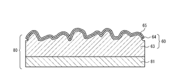
- an optical body 60 As shown in FIG. 1, an optical body (hereinafter sometimes referred to as “optical body according to the present embodiment”) 60 according to an embodiment of the present invention includes at least a fine uneven layer 63. Moreover, the optical body which concerns on this embodiment can be further equipped with a 1st transparent inorganic layer, a 2nd transparent inorganic layer, a 3rd transparent inorganic layer, an antifouling coating layer, another layer, etc. as needed.
- the fine uneven layer is a layer having a fine uneven structure on at least one surface.
- the uneven structure may be formed in a regular pattern or may be formed randomly.
- the fine uneven surface in the fine uneven layer has an arithmetic average roughness Ra of 0.2 ⁇ m or less in a rectangular region of 35.3 ⁇ m ⁇ 26.5 ⁇ m.
- ratio of surface area to .45 ⁇ m 2) ( ⁇ m 2) (hereinafter sometimes referred to as "specific surface area”.) is 1.04 to 1.5.
- the present inventors surprisingly set the average length RSm and / or the specific surface area of the roughness curvilinear element within the above-mentioned range, while making the arithmetic average roughness Ra of the micro uneven surface 0.2 ⁇ m or less.
- unevenness having a shape smaller than the wavelength of the visible light region can be formed, and a part of the light can be transmitted without changing the traveling direction, and the transmitted image definition can be enhanced. It has been found that an optical body compatible with is obtained.
- the fine asperity surface in the fine asperity layer has an average length RSm of the roughness curvilinear element of 10 ⁇ m or less and a specific surface area of 1.04 to 1.5. It is preferable that it is the following.
- Arithmetic mean roughness Ra of the fine asperity surface in the fine asperity layer is preferably 0.18 ⁇ m or less, more preferably 0.14 ⁇ m or less from the viewpoint of achieving both higher antiglare property and viewability. preferable.
- the arithmetic average roughness Ra of the fine asperity surface in the fine asperity layer is preferably 0.08 ⁇ m or more, and more preferably 0.09 ⁇ m or more, from the viewpoint of further enhancing the antiglare property.
- the average length RSm of the surface roughness curvilinear element of the surface with fine asperities in the surface asperity layer is preferably 6 ⁇ m or less from the viewpoint of further enhancing the clearness of the transmitted image.
- the average length RSm of the surface roughness curvilinear element of the surface asperity in the surface asperity layer is 2 ⁇ m or more from the viewpoint of achieving both higher antiglare property and viewability, and from the viewpoint of enhancing the physical strength of the surface asperity. Is preferred.
- the specific surface area of the fine asperity surface in the fine asperity layer is preferably 1.1 or more from the viewpoint of further enhancing the antiglare property. Moreover, it is preferable that the specific surface area of the fine uneven
- the fine uneven layer can be formed by, for example, a shape transfer method, a phase separation method, a filler dispersion method, or the like.
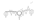
- a method of forming a fine uneven layer by a shape transfer method will be described with reference to FIG.
- FIG. 2 is a schematic diagram which shows the shape transfer method which is an example of the method for forming the fine concavo-convex layer of the optical body which concerns on this embodiment.
- the shape transfer device 1 shown in FIG. 2 includes a master 2, a base material supply roll 51, a winding roll 52, guide rolls 53 and 54, a nip roll 55, a peeling roll 56, a coating device 57, and a light source. And 58.
- the base material supply roll 51 is a roll in which a sheet-like base material 61 is wound in a roll shape, and the winding roll 52 winds up the base material 61 on which the resin layer 62 to which the fine concavo-convex structure 23 is transferred is laminated. It is a role.
- the guide rolls 53 and 54 are rolls for transporting the base 61.
- the nip roll 55 is a roll for closely adhering the base material 61 on which the resin layer 62 is laminated to the cylindrical master 2
- the peeling roll 56 is a resin layer after the fine concavo-convex structure 23 is transferred to the resin layer 62.
- 62 is a roll for peeling the base material 61 on which the 62 is laminated from the master 2.
- the substrate 61 may be, for example, a plastic substrate such as a PET resin or a polycarbonate resin, and may be a plastic transparent film.
- the coating device 57 includes a coating unit such as a coater, and applies a composition (a UV curable resin composition) containing a UV curable resin to the substrate 61 to form a resin layer 62.
- the coating device 57 may be, for example, a gravure coater, a wire bar coater, or a die coater.
- the light source 58 is a light source that emits ultraviolet light, and may be, for example, an ultraviolet lamp.
- An ultraviolet curable resin is a resin which is reduced in fluidity by being irradiated with ultraviolet light and is cured. Specific examples thereof include acrylic resins. Moreover, the ultraviolet curable resin composition may contain an initiator, a filler, a functional additive, a solvent, an inorganic material, a pigment, an antistatic agent, a sensitizing dye, etc. as needed.
- the sheet-like base material 61 is continuously delivered from the base material supply roll 51 via the guide roll 53.
- the ultraviolet curable resin composition is applied to the base material 61 that has been sent out by the coating device 57, and the resin layer 62 is laminated on the base material 61.
- the base 61 on which the resin layer 62 is laminated is in close contact with the master 2 by the nip roll 55.
- the fine concavo-convex structure 23 formed on the outer peripheral surface of the master 2 is transferred to the resin layer 62.
- the resin layer 62 is cured by the irradiation of light from the light source 58.
- the base material 61 on which the cured resin layer 62 is laminated is peeled off from the master 2 by the peeling roll 56 and taken up by the winding roll 52 via the guide roll 54.
- a shape transfer device 1 it is possible to continuously form a fine uneven layer having a fine uneven surface.
- Ra, RSm, and the specific surface area of the fine uneven surface can be adjusted, for example, by appropriately changing the fine uneven structure 23 of the master 2.
- the base material and the ultraviolet curable resin are prepared, and the fine asperity layer is formed on the base material using the resin (that is, as shown in FIG. 1, the fine asperity layer)
- the layer 63 is composed of the base material 61 and the resin layer 62 having a fine concavo-convex structure
- the fine concavo-convex layer of the optical body of the present invention is not limited thereto.
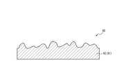
- UV curable resin or thermosetting resin The fine uneven structure may be directly formed on a base material made of a resin such as (that is, as shown in FIG. 3, the fine uneven layer 63 may be formed of only the base material 61).
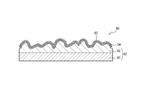
- the optical body 60 preferably includes the first transparent inorganic layer 64 on the surface of the fine asperity layer 63.
- the first transparent inorganic layer 64 has transparency and can have a function of absorbing light of a predetermined wavelength, for example.
- the first transparent inorganic layer 64 can be formed by, for example, a sputtering method or a CVD method.
- “transparent” or “having transparency” means that the transmitted image definition is high and the image can be clearly viewed through the optical body.
- the main component of the first transparent inorganic layer is preferably an inorganic compound having a band gap of 2.8 eV or more and 4.8 eV or less.
- the band gap represents the wavelength of the absorption edge, and in a broad sense, it indicates that the light below the wavelength corresponding to the band gap is absorbed, and the light above the wavelength corresponding to the band gap is transmitted.
- the main component of the first transparent inorganic layer is more preferably an inorganic compound having a band gap of 3.0 eV or more and 3.7 eV or less (approximately 340 nm or more and 420 nm or less in wavelength conversion).
- the main component of the first transparent inorganic layer is 3.0 eV or more and 3.4 eV or less (approximately 360 nm or more in wavelength conversion) It is more preferable that it is an inorganic compound having a band gap of 420 nm or less.
- a "main component" shall refer to the component with most content.
- the inorganic compound having a band gap of 2.8 eV or more and 4.8 eV or less include ZnO, CeO 2 , TiO 2 , SnO 2 , In 2 O 3 , Nb 2 O 5 , and Ta 2 O 5 . SiC, ZnS and the like can be mentioned. Further, specific examples of the inorganic compound having a band gap of 3.0 eV or more and 3.7 eV or less include ZnO, CeO 2 , TiO 2 , Nb 2 O 5 , SiC, and ZnS. Further, specific examples of the inorganic compound having a band gap of 3.0 eV or more and 3.4 eV or less include ZnO, CeO 2 and the like.
- the first transparent inorganic layer preferably contains at least one of ZnO and CeO 2 .
- ZnO includes ZnO doped with aluminum (Al) and ZnO doped with other elements.
- CeO 2 is doped with gadolinium (Gd) -doped CeO 2 (sometimes collectively referred to as “CeGdO 2” ) (eg, Ce 0.9 Gd 0.1 O 2 ), samarium (Sm) It has been CeO 2, and is intended to include CeO 2 doped with other elements.
- the thickness of the first transparent inorganic layer is preferably 70 nm or more, and preferably 400 nm or less.
- the thickness of the first transparent inorganic layer is 70 nm or more, sufficiently high ultraviolet light absorption characteristics can be obtained, and when it is 400 nm or less, the risk of productivity decrease and crack generation can be suppressed. it can.
- the thickness of the first transparent inorganic layer is more preferably 100 nm or more, and more preferably 300 nm or less.
- the optical body 60 in addition to the first transparent inorganic layer 64, preferably includes a second transparent inorganic layer 65 on the first transparent inorganic layer 64. .
- the second transparent inorganic layer has transparency, may be water-repellent or hydrophilic, and can be formed by, for example, a sputtering method or a CVD method.
- the main component of the second transparent inorganic layer preferably has a band gap larger than the band gap of the main component of the first transparent inorganic layer, and more specifically, the band gap of the main component of the first transparent inorganic layer Is preferably an inorganic compound having a large band gap of 4.0 eV or more.
- the band gap of the main component of the second transparent inorganic layer is larger than the band gap of the main component of the first transparent inorganic layer, preferably 4.0 eV or more, the stain resistance of the first transparent inorganic layer is improved.
- the antiglare property of the obtained optical body can be improved.
- the second transparent inorganic layer preferably contains at least one of SiO 2 , SiN, SiON and MgF 2 .
- the second transparent inorganic layer more preferably contains at least SiO 2 .
- the thickness of the second transparent inorganic layer is preferably 20 nm or more, and preferably 200 nm or less.
- the thickness of the second transparent inorganic layer is 20 nm or more and 200 nm or less, the reflectance can be sufficiently reduced, and the antiglare property can be more effectively improved.
- the thickness of the second transparent inorganic layer is more preferably 40 nm or more, and more preferably 100 nm or less.
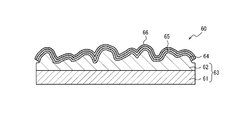
- the optical body according to the present embodiment has a third transparent inorganic layer 66 on the second transparent inorganic layer 65. It is preferable to further comprise By providing the third transparent inorganic layer, the deterioration of the first transparent inorganic layer and the second transparent inorganic layer due to chemicals can be suppressed.
- the third transparent inorganic layer has transparency, may be water-repellent or hydrophilic, and can be formed by, for example, a sputtering method or a CVD method.
- the third transparent inorganic layer can contain at least one of SiO 2 , SiN, SiON and MgF 2 as a main component.
- the third transparent inorganic layer preferably further contains ZrO 2 , Nb 2 O 5 or SnO 2 as an additional component.
- the ratio of the said additional component in a 3rd transparent inorganic layer is 6 to 50 mass%.
- the proportion of the additional component is 6% by mass or more, the effect of improving the chemical resistance can be sufficiently obtained, and by being 50% by mass or less, the refractive index with the second transparent inorganic layer It is possible to keep the difference moderate and avoid the difficulty of optical design.
- the ratio of the additional component in the third transparent inorganic layer is more preferably 13% by mass or more, still more preferably 20% by mass or more, and 30% by mass or less Is more preferred.
- the additional components may be used alone or in combination of two or more.
- the third transparent inorganic layer preferably has a thickness of 20 nm or more. When the thickness of the third transparent inorganic layer is 20 nm or more, a sufficiently high chemical resistance can be obtained.
- the third transparent inorganic layer preferably has a thickness of 200 nm or less. When the thickness of the third transparent inorganic layer is 200 nm or less, it is possible to suppress the risk of productivity decrease and crack generation. From the same viewpoint, the thickness of the third transparent inorganic layer is more preferably 100 nm or less.
- the optical body which concerns on this embodiment equips the outermost surface by the side of the fine concavo-convex surface of a fine concavo-convex layer with an antifouling coat layer.
- the optical body according to the present embodiment preferably includes an antifouling coating layer on the fine concavo-convex layer, on the second transparent inorganic layer, or on the third transparent inorganic layer.
- antifouling coat layer it is preferably provided on the second transparent inorganic layer or the third transparent inorganic layer mainly comprising SiO 2.
- the main component of the antifouling coating layer may be water-repellent or hydrophilic, and may be oil- or lipophilic.
- the main component of the antifouling coating layer is preferably water repellent and oil repellent.
- the antifouling coating layer preferably has a pure water contact angle of 110 ° or more, and more preferably 115 ° or more.
- the main component of the antifouling coating layer is preferably a perfluoropolyether.
- the antifouling coating layer preferably has a thickness of 5 nm or more, and preferably 20 nm or less, for example, 10 nm.
- the thickness of the antifouling coating layer is 5 nm or more, the antifouling property of the optical body can be sufficiently enhanced, and when it is 20 nm or less, the burying of the uneven structure of the fine uneven layer can be avoided. it can.
- the optical body according to the present embodiment is not particularly limited, and may have other layers in addition to the layers described above.
- the optical body according to the present embodiment may be provided with an adhesion layer between the fine concavo-convex layer and the first transparent inorganic layer in order to firmly adhere the layer.
- an adhesion layer for example, a SiO x layer can be mentioned, and the thickness can be, for example, 2 nm or more and 10 nm or less.
- the adhesion layer can be formed, for example, by sputtering or CVD.
- the optical body which concerns on this embodiment equips the surface on the opposite side to the fine concavo-convex surface of the fine concavo-convex layer with the adhesion layer which absorbs visible light.
- Visible light which passes through (the optional first transparent inorganic layer 64 and the fine concavo-convex layer 63 and is incident on the adhesive layer 84, and (the optional first transparent inorganic layer 64), the fine concavo-convex layer 63 and the adhesive layer
- visible light and the like reflected by the glass substrate 81 and incident on the adhesive layer 84 are efficiently absorbed to reduce the visible light transmittance, and the antiglare property is further improved while maintaining high viewability. can do.
- the adhesion layer which absorbs visible light can be prepared, for example, using a material having adhesiveness, in which a coloring agent such as a dye or a pigment which absorbs visible light is dispersed at an arbitrary ratio.
- a coloring agent such as a dye or a pigment which absorbs visible light
- colorants such as dyes or pigments are contained.
- a substrate that absorbs visible light or an inorganic film that absorbs visible light, such as DLC, may be stacked on the fine uneven layer.
- the optical body according to the present embodiment preferably has a glossiness of 40 or less at a measurement angle of 20 °.
- the glossiness at a measurement angle of 20 ° is 40 or less, the antiglare property of the optical body can be made sufficiently high.
- the glossiness at a measurement angle of 20 ° of the optical body is more preferably 30 or less, and still more preferably 20 or less.
- the glossiness in 20 degrees of measurement angles of an optical body can be measured by the method used in the Example.
- the optical body according to the present embodiment preferably has a transmitted image definition of 50% or more at an optical comb width of 2 mm.
- the transmitted image definition in an optical comb width of 2 mm is 50% or more, the viewability of the optical body can be made sufficiently high.
- the transmitted image definition at an optical comb width of 2 mm of the optical body is more preferably 70% or more, and still more preferably 80% or more.
- the transmitted image clearness in 2 mm of optical comb widths of an optical body can be measured by the method used in the Example.
- the optical body according to the present embodiment preferably has a total haze of 15% or more and 60% or less.
- the total haze is 15% or more, the antiglare property can be effectively enhanced, and when the total haze is 60% or less, the viewability can be effectively enhanced.
- the total haze of the optical body is more preferably 50% or less.
- the optical body according to the present embodiment preferably has an internal haze of 4% or less. By the internal haze being 4% or less, the view can be further enhanced. From the same viewpoint, the internal haze of the optical body is more preferably 2% or less.
- the total haze and internal haze of an optical body can be measured by the method used in the Example.
- the optical body according to the present embodiment preferably has a transmittance of 10% or less, more preferably 6% or less, and still more preferably 3% or less.
- the transmittance of light with a wavelength of 320 nm of the optical body is 10% or less, deterioration such as yellowing of the base material due to ultraviolet light can be effectively suppressed, and adhesion durability between the base material and the resin layer Can be improved.
- the transmittance of light of wavelength 320 nm of the optical body can be measured, for example, using “V-560” manufactured by JASCO Corporation.
- window material A window material according to an embodiment of the present invention (hereinafter sometimes referred to as “window material according to the present embodiment”) includes a glass substrate and the above-described optical body. Specifically, as shown in FIG. 7, the window member 80 according to the present embodiment has the optical body 60 and the glass substrate 81 described above, and the surface on the opposite side to the fine asperity surface of the optical body 60 is a glass substrate It can be made to laminate so that 81 may be faced. As described above, the window material according to the present embodiment includes at least the above-described optical body, and is excellent in both the antiglare property and the viewability, so window glass for buildings such as high-rise buildings and houses, window glass for vehicles, etc. Can be suitably used. In addition, the window material which concerns on this embodiment may be equipped with the optical body mentioned above only on the single side
- the gloss at a measurement angle of 20 °, the transmitted image sharpness at an optical comb width of 2 mm, the total haze, the internal haze, and the light of wavelength 320 nm in the window material according to this embodiment are respectively the same as those described above for the optical body.
- the window material according to the present embodiment may be a multilayer glass.
- double glazing is inferior in anti-glare property to single-layer glass, but the window material according to the present embodiment is highly anti-glare even if it is double glazing because it is provided with the optical body described above. Can bring
- a plurality of glass substrates (82, 83) are laminated with the spacer 85 at the periphery, and a space is formed between the glass substrates, as shown in FIG. Refers to a glass having a structure.
- window material 80 concerning this embodiment which is a double glazing is an outdoor side of glass substrate 82 which becomes an outdoor side when installed in a building etc. as window glass.
- the optical body 60 may be provided only on the surface, and as shown in (b) to (d) of FIG. 8, the optical body 60 is provided on the surface on the outdoor side of the glass substrate 82 serving as the outdoor side.
- the optical body 60 may be provided on one side and / or both sides of the glass substrate 83 on the indoor side, and as shown in (e) to (h) of FIG.
- the optical body is provided on both sides of the substrate 82, and optionally, the optical body 60 may be provided on one side and / or both sides of the glass substrate 83 which is the indoor side.
- the window material which concerns on this embodiment is a multilayer glass
- an optical body is provided in the surface of the outdoor side of the glass substrate which becomes an outdoor side when it installs in a building etc. as window glass. It is particularly preferable to provide an adhesive layer that absorbs visible light on the surface (more specifically, between the optical body and the glass substrate) of the optical body on the opposite side to the microrelief surface.
- the visible light that passes through the optical body and enters the adhesive layer passes through the optical body and the adhesive layer, and then on the indoor side surface of the glass substrate on the outdoor side After transmitting through visible light that is reflected and enters the adhesive layer, and through the optical body, the adhesive layer, and the glass substrate on the outdoor side, it is reflected by the glass substrate on the indoor side and transmitted through the glass substrate on the outdoor side to the adhesive layer. It is possible to efficiently absorb incident visible light and the like to reduce the visible light transmittance, and to solve the antiglare problem that double-layered glass can frequently encounter, while maintaining high view.
- Examples 1 to 5, Comparative Examples 1 to 2 A resin layer having a fine concavo-convex structure is formed on a PET base material (Toyobo Co., Ltd., “A4300”, 75 ⁇ m thick) by a shape transfer method using a composition containing an acrylic UV curable resin And got an optical body.
- a shape transfer method using a composition containing an acrylic UV curable resin And got an optical body.
- each parameter (Ra: Arithmetic average roughness ( ⁇ m), RSm: average length of roughness curvilinear element, specific surface area) concerning the surface of the optical body is shown in Table 1
- the conditions of the shape transfer method were appropriately adjusted such as changing the surface shape of the master so as to obtain the values shown.
- Specific conditions include software: MtroPro 8.3.5, Acquisition Mode: Scan, Scan Type: Bipolar, zoom lens: 2 ⁇ , objective lens: 200 ⁇ , mode: High 2G, surface correction: Cylinder, Camera Mode: It was set to 640 ⁇ 480 210 Hz.
- the said measurement was performed in the 35.3 micrometers x 26.5 micrometers rectangular area
- Transmission image definition T is 70% or more ⁇ Transmission image definition T is 50% or more and less than 70% ⁇ Transmission image definition T is less than 50% ⁇ ⁇
- Ra is 0.2 ⁇ m or less, and at least one of RSm and the specific surface area is within the predetermined range, so it is possible to achieve both the antiglare property and the viewability. I know that I can do it.
- an optical body excellent in antiglare property and viewability and a window material excellent in antiglare property and viewability.
Landscapes
- Physics & Mathematics (AREA)
- Engineering & Computer Science (AREA)
- Civil Engineering (AREA)
- Structural Engineering (AREA)
- General Physics & Mathematics (AREA)
- Optics & Photonics (AREA)
- Laminated Bodies (AREA)
- Securing Of Glass Panes Or The Like (AREA)
- Optical Elements Other Than Lenses (AREA)
Abstract
防眩性及び眺望性に優れる光学体を提供する。光学体は、微細凹凸層を備え、微細凹凸表面の35.3μm×26.5μmの長方形領域において、算術平均粗さRaが0.2μm以下であり、且つ、粗さ曲線要素の平均長さRSmが10μm以下であるか、又は、当該長方形の面積に対する表面積の割合が1.04以上1.5以下である、ことを特徴とする。
Description
本発明は、光学体、及び窓材に関するものであり、より具体的には、高い防眩性と眺望性とが両立した光学体、及び、これを備える窓材に関するものである。
近年、高層ビルやタワーマンション等を含む建築物においては、搭載される窓ガラス等に光が反射し、他の近隣の建築物の利用者に眩しさをもたらす、いわゆる反射光害が頻繁に問題となっている。そのため、建築物の建設に当たっては、上述した反射光害への十分な対策を講じることが求められている。
ここで、建築物の窓ガラスからの反射光の眩しさ対策としては、例えば、建築物の壁面にルーバーなどを設置して反射光を直接遮る方法が挙げられる。しかし、ルーバーの設置は、工事が大掛かりでコストが高く、建築物のデザイン性にも影響することから、所有者に敬遠されることが多い。
一方、建築物の窓ガラスの防眩性を向上する方法としては、上述した方法以外に、窓ガラスにフィルムを貼って反射特性を改善する方法が挙げられる。
例えば、防眩性を含む反射特性を改善し得るフィルムとして、特許文献1は、基材フィルム上に紫外線硬化樹脂を用いてランダム凹凸形状面を有するAG(アンチグレア)層を形成するとともに、その凹凸形状を平坦化するように低屈折率樹脂からなる層を形成することにより、可視光域での反射率をフラットにしつつ、ディスプレイに貼り付けた場合に黒を際立たせることができる光学フィルムが得られることを開示している。
また、特許文献2は、基材フィルム上に紫外線硬化樹脂を用いて金型表面の凹凸を転写成形してフィルムを得る際に、所定粒径のブラスト粒子を衝打させた金型表面を用いることにより、高い透過鮮明度を保ちつつギラツキが低減したフィルムが得られることを開示している。
しかしながら、上述した従来のフィルムは、いずれも、パソコンや液晶テレビなどの液晶パネルの表示面に設けられる偏光板に主として用いられるものである。そして、上述した従来のフィルムは、いずれも、窓ガラスに用いて高い防眩性と眺望性とを両立させる観点では、改善の余地がある。
本発明は、従来における前記諸問題を解決し、以下の目的を達成することを課題とする。即ち、本発明の目的は、防眩性及び眺望性に優れる光学体、並びに、防眩性及び眺望性に優れる窓材を提供することにある。
本発明者らは、前記目的を達成すべく、フィルムに限定することなく、鋭意検討を行った。その結果、微細凹凸表面の粗さの特性の適正化を図ることで、高い防眩性及び眺望性を両立させられることを見出し、本発明の完成に至った。
本発明は、本発明者らによる前記知見に基づくものであり、前記課題を解決するための手段としては以下の通りである。即ち、
<1> 微細凹凸層を備える光学体であって、
微細凹凸表面の35.3μm×26.5μmの長方形領域において、
算術平均粗さRaが0.2μm以下であり、且つ、
粗さ曲線要素の平均長さRSmが10μm以下であるか、又は、当該長方形の面積に対する表面積の割合が1.04以上1.5以下である、
ことを特徴とする、光学体である。
<1> 微細凹凸層を備える光学体であって、
微細凹凸表面の35.3μm×26.5μmの長方形領域において、
算術平均粗さRaが0.2μm以下であり、且つ、
粗さ曲線要素の平均長さRSmが10μm以下であるか、又は、当該長方形の面積に対する表面積の割合が1.04以上1.5以下である、
ことを特徴とする、光学体である。
<2> 第1透明無機層と、第2透明無機層とを更に備え、
前記第1透明無機層は、前記微細凹凸層の微細凹凸表面上に配置され、前記第2透明無機層は、前記第1透明無機層上に配置される、<1>に記載の光学体である。
前記第1透明無機層は、前記微細凹凸層の微細凹凸表面上に配置され、前記第2透明無機層は、前記第1透明無機層上に配置される、<1>に記載の光学体である。
<3> 前記第1透明無機層が、ZnO及びCeO2の少なくともいずれかを含有し、
前記第2透明無機層が、SiO2、SiN、SiON及びMgF2の少なくともいずれかを含有する、前記<2>に記載の光学体である。
前記第2透明無機層が、SiO2、SiN、SiON及びMgF2の少なくともいずれかを含有する、前記<2>に記載の光学体である。
<4> 全ヘイズが15%以上60%以下であり、内部ヘイズが4%以下であり、測定角20°における光沢度が40以下であり、且つ、光学櫛幅2mmにおける透過像鮮明度が50%以上である、前記<1>~<3>のいずれかに記載の光学体である。
<5> 前記第2透明無機層上に第3透明無機層を更に備える、前記<2>~<4>のいずれかに記載の光学体である。
<6> ガラス基板と、前記<1>~<5>のいずれかに記載の光学体とを備える、ことを特徴とする、窓材である。
本発明によれば、従来における前記諸問題を解決し、前記目的を達成することができ、防眩性及び眺望性に優れる光学体、並びに、防眩性及び眺望性に優れる窓材を提供することができる。
(光学体)
図1に示すように、本発明の一実施形態に係る光学体(以下、「本実施形態に係る光学体」と称することがある。)60は、少なくとも、微細凹凸層63を備える。また、本実施形態に係る光学体は、更に必要に応じて、第1透明無機層、第2透明無機層、第3透明無機層、防汚コート層、その他の層などを備えることができる。
図1に示すように、本発明の一実施形態に係る光学体(以下、「本実施形態に係る光学体」と称することがある。)60は、少なくとも、微細凹凸層63を備える。また、本実施形態に係る光学体は、更に必要に応じて、第1透明無機層、第2透明無機層、第3透明無機層、防汚コート層、その他の層などを備えることができる。
<微細凹凸層>
微細凹凸層は、少なくとも一方の表面に微細な凹凸構造を有する層である。この凹凸構造は、規則的なパターンで形成されていてもよく、ランダムに形成されていてもよい。
微細凹凸層は、少なくとも一方の表面に微細な凹凸構造を有する層である。この凹凸構造は、規則的なパターンで形成されていてもよく、ランダムに形成されていてもよい。
微細凹凸層における微細凹凸表面は、35.3μm×26.5μmの長方形領域において、算術平均粗さRaが、0.2μm以下である。また、微細凹凸層における微細凹凸表面は、当該長方形領域において、粗さ曲線要素の平均長さRSmが10μm以下であるか、又は、当該長方形の面積(即ち、35.3μm×26.5μm=935.45μm2)に対する表面積(μm2)の割合(以下、「比表面積」と称することがある。)が1.04以上1.5以下である。本発明者らは、驚くべきことに、微細凹凸表面の算術平均粗さRaを0.2μm以下としつつ、粗さ曲線要素の平均長さRSm及び/又は比表面積を上述した範囲内にすることにより、可視光域の波長よりも小さい形状の凹凸が形成され得、一部の光を進行方向を変えずに透過させて、透過像鮮明度を高めることができ、防眩性と眺望性とが両立した光学体が得られることを見出した。
また、微細凹凸層における微細凹凸表面は、防眩性及び眺望性をより高める観点から、粗さ曲線要素の平均長さRSmが10μm以下であり、且つ、比表面積が1.04以上1.5以下であることが好ましい。
微細凹凸層における微細凹凸表面の算術平均粗さRaは、より高い防眩性及と眺望性とを両立させる観点から、0.18μm以下であることが好ましく、0.14μm以下であることがより好ましい。一方、微細凹凸層における微細凹凸表面の算術平均粗さRaは、防眩性をより高める観点から、0.08μm以上であることが好ましく、0.09μm以上であることがより好ましい。
また、微細凹凸層における微細凹凸表面の粗さ曲線要素の平均長さRSmは、透過像鮮明度を一層高める観点から、6μm以下であることが好ましい。また、微細凹凸層における微細凹凸表面の粗さ曲線要素の平均長さRSmは、より高い防眩性及と眺望性とを両立させる観点、及び微細凹凸の物理強度を高める観点から、2μm以上であることが好ましい。
また、微細凹凸層における微細凹凸表面の比表面積は、防眩性を一層高める観点から、1.1以上であることが好ましい。また、微細凹凸層における微細凹凸表面の比表面積は、眺望性を一層高める観点から、1.4以下であることが好ましい。
上述したRa、RSm及び比表面積は、実施例で用いた方法により、測定することができる。
ここで、微細凹凸層は、例えば、形状転写法、相分離法、フィラー分散法などにより、形成することができる。以下、一例として、形状転写法による微細凹凸層の形成方法について、図2を参照して説明する。
図2は、本実施形態に係る光学体の微細凹凸層を形成するための方法の一例である、形状転写法を示す模式図である。図2に示される形状転写装置1は、原盤2と、基材供給ロール51と、巻取ロール52と、ガイドロール53、54と、ニップロール55と、剥離ロール56と、塗布装置57と、光源58とを備える。
基材供給ロール51は、シート状の基材61がロール状に巻かれたロールであり、巻取ロール52は、微細凹凸構造23が転写された樹脂層62を積層した基材61を巻き取るロールである。また、ガイドロール53、54は、基材61を搬送するロールである。ニップロール55は、樹脂層62が積層された基材61を円筒形状の原盤2に対して密着させるロールであり、剥離ロール56は、微細凹凸構造23が樹脂層62に転写された後、樹脂層62が積層された基材61を原盤2から剥離するロールである。ここで、基材61は、例えば、PET樹脂又はポリカーボネート樹脂などのプラスチック製の基材とすることができ、また、プラスチック製の透明なフィルムとすることができる。
塗布装置57は、コーターなどの塗布手段を備え、紫外線硬化性樹脂を含む組成物(紫外線硬化性樹脂組成物)を基材61に塗布し、樹脂層62を形成する。塗布装置57は、例えば、グラビアコーター、ワイヤーバーコーター又はダイコーターなどであってもよい。また、光源58は、紫外光を発する光源であり、例えば、紫外線ランプなどとすることができる。
紫外線硬化性樹脂は、紫外線が照射されることにより流動性が低下し、硬化する樹脂であり、具体的には、アクリル系樹脂などが挙げられる。また、紫外線硬化性樹脂組成物は、必要に応じて、開始剤、フィラー、機能性添加剤、溶剤、無機材料、顔料、帯電防止剤又は増感色素などを含有していてもよい。
形状転写装置1では、まず、基材供給ロール51からガイドロール53を介して、シート状の基材61が連続的に送出される。送出された基材61に対して、塗布装置57により紫外線硬化性樹脂組成物が塗布され、基材61に樹脂層62が積層される。また、樹脂層62が積層された基材61は、ニップロール55により、原盤2に密着する。これにより、原盤2の外周面に形成された微細凹凸構造23が樹脂層62に転写される。微細凹凸構造23が転写された後、樹脂層62は、光源58からの光の照射により硬化する。続いて、硬化した樹脂層62が積層された基材61は、剥離ロール56により原盤2から剥離され、ガイドロール54を介して、巻取ロール52によって巻き取られる。
このような形状転写装置1により、微細凹凸表面を有する微細凹凸層を連続的に形成することができる。ここで、微細凹凸表面のRa、RSm及び比表面積は、例えば、原盤2の微細凹凸構造23を適宜変更することにより、調整することができる。
このような形状転写装置1により、微細凹凸表面を有する微細凹凸層を連続的に形成することができる。ここで、微細凹凸表面のRa、RSm及び比表面積は、例えば、原盤2の微細凹凸構造23を適宜変更することにより、調整することができる。
なお、上述した形状転写法では、基材と紫外線硬化性樹脂とを準備し、当該樹脂を用いて基材上に微細凹凸層を形成している(即ち、図1に示すように、微細凹凸層63が、基材61と微細凹凸構造を有する樹脂層62とからなる)が、本発明の光学体の微細凹凸層は、これに制限されず、例えば、紫外線硬化性樹脂や熱硬化性樹脂等の樹脂からなる基材に微細凹凸構造を直接形成したもの(即ち、図3に示すように、微細凹凸層63が、基材61のみからなるもの)であってもよい。
<第1透明無機層>
また、図4に示すように、本実施形態に係る光学体60は、微細凹凸層63の微細凹凸表面上に第1透明無機層64を備えることが好ましい。この第1透明無機層64は、透明性を有するとともに、例えば、所定の波長の光を吸収する機能を有することができる。また、第1透明無機層64は、例えば、スパッタ法又はCVD法により形成することができる。
なお、本明細書において「透明」又は「透明性を有する」とは、透過像鮮明度が高く、光学体を通して像が明確に視認できることを指すものとする。
また、図4に示すように、本実施形態に係る光学体60は、微細凹凸層63の微細凹凸表面上に第1透明無機層64を備えることが好ましい。この第1透明無機層64は、透明性を有するとともに、例えば、所定の波長の光を吸収する機能を有することができる。また、第1透明無機層64は、例えば、スパッタ法又はCVD法により形成することができる。
なお、本明細書において「透明」又は「透明性を有する」とは、透過像鮮明度が高く、光学体を通して像が明確に視認できることを指すものとする。
第1透明無機層の主成分は、2.8eV以上4.8eV以下のバンドギャップを有する無機化合物であることが好ましい。ここで、バンドギャップは、吸収端の波長を表し、広義的に、バンドギャップに相当する波長を下回る光を吸収し、バンドギャップに相当する波長以上の光を透過することを示す。そして、上述した2.8eV以上4.8eV以下のバンドギャップは、Planck定数(6.626×10⁻³⁴J・s)及び光速度(2.998×10⁸m/s)を用いて得られる波長λとバンドギャップエネルギーEとの関係式:「λ(nm)=1240/E(eV)」から、おおよそ、紫外領域と可視領域との境界である260nm以上440nm以下の範囲内に吸収端の波長があることを示している。従って、上述した無機化合物を第1透明無機層に用いることにより、透明性と紫外線吸収特性とを両立することができる。同様の観点から、第1透明無機層の主成分は、3.0eV以上3.7eV以下(波長換算でおよそ340nm以上420nm以下)のバンドギャップを有する無機化合物であることがより好ましい。また、生産性の低下やクラック発生のリスクを抑制するために薄膜化を図ることも踏まえれば、第1透明無機層の主成分は、3.0eV以上3.4eV以下(波長換算でおよそ360nm以上420nm以下)のバンドギャップを有する無機化合物であることがより好ましい。
なお、本明細書において「主成分」とは、含有量が最も多い成分を指すものとする。
なお、本明細書において「主成分」とは、含有量が最も多い成分を指すものとする。
なお、2.8eV以上4.8eV以下のバンドギャップを有する無機化合物としては、具体的に、ZnO、CeO2、TiO2、SnO2、In2O3、Nb2O5、Ta2O5、SiC、ZnSなどが挙げられる。また、3.0eV以上3.7eV以下のバンドギャップを有する無機化合物の例としては、具体的に、ZnO、CeO2、TiO2、Nb2O5、SiC、ZnSなどが挙げられる。更に、3.0eV以上3.4eV以下のバンドギャップを有する無機化合物の例としては、具体的に、ZnO、CeO2などが挙げられる。以上を考慮して、第1透明無機層は、ZnO及びCeO2の少なくともいずれかを含有することが好ましい。
なお、本明細書において、「ZnO」は、アルミニウム(Al)でドープされたZnO、及び、その他の元素でドープされたZnOを含むものとする。
また、本明細書において、「CeO2」は、ガドリニウム(Gd)でドープされたCeO2(CeGdO2と総称されることがある)(Ce0.9Gd0.1O2など)、サマリウム(Sm)でドープされたCeO2、及び、その他の元素でドープされたCeO2を含むものとする。
また、これら無機化合物は、一種単独で第1透明無機層に用いてもよく、二種以上を組み合わせて第1透明無機層に用いてもよい。
なお、本明細書において、「ZnO」は、アルミニウム(Al)でドープされたZnO、及び、その他の元素でドープされたZnOを含むものとする。
また、本明細書において、「CeO2」は、ガドリニウム(Gd)でドープされたCeO2(CeGdO2と総称されることがある)(Ce0.9Gd0.1O2など)、サマリウム(Sm)でドープされたCeO2、及び、その他の元素でドープされたCeO2を含むものとする。
また、これら無機化合物は、一種単独で第1透明無機層に用いてもよく、二種以上を組み合わせて第1透明無機層に用いてもよい。
第1透明無機層は、厚みが、70nm以上であることが好ましく、また、400nm以下であることが好ましい。第1透明無機層の厚みが70nm以上であることにより、十分に高い紫外線吸収特性を得ることができ、また、400nm以下であることにより、生産性の低下やクラック発生のリスクを抑制することができる。同様の観点から、第1透明無機層の厚みは、100nm以上であることがより好ましく、また、300nm以下であることがより好ましい。
<第2透明無機層>
また、図4に示すように、本実施形態に係る光学体60は、第1透明無機層64に加え、当該第1透明無機層64の上に、第2透明無機層65を備えることが好ましい。第2透明無機層を備えることにより、第1透明無機層への雨などによる汚れの付着を防止することができる。この第2透明無機層は、透明性を有し、撥水性であっても親水性であってもよく、また、例えば、スパッタ法又はCVD法により形成することができる。
また、図4に示すように、本実施形態に係る光学体60は、第1透明無機層64に加え、当該第1透明無機層64の上に、第2透明無機層65を備えることが好ましい。第2透明無機層を備えることにより、第1透明無機層への雨などによる汚れの付着を防止することができる。この第2透明無機層は、透明性を有し、撥水性であっても親水性であってもよく、また、例えば、スパッタ法又はCVD法により形成することができる。
第2透明無機層の主成分は、第1透明無機層の主成分のバンドギャップよりも大きいバンドギャップを有することが好ましく、より具体的には、第1透明無機層の主成分のバンドギャップよりも4.0eV以上大きいバンドギャップを有する無機化合物であることが好ましい。第2透明無機層の主成分のバンドギャップが第1透明無機層の主成分のバンドギャップよりも大きい、好適には4.0eV以上大きいことにより、第1透明無機層の防汚性の向上に加えて、得られる光学体の防眩性を向上させることができる。
具体的に、好ましい第2透明無機層の主成分としては、SiO2、SiN、SiON、MgF2などの無機化合物が挙げられる。言い換えると、第2透明無機層は、SiO2、SiN、SiON及びMgF2の少なくともいずれかを含有することが好ましい。また、第2透明無機層は、少なくともSiO2を含有することがより好ましい。
これら無機化合物は、一種単独で第2透明無機層に用いてもよく、二種以上を組み合わせて第2透明無機層に用いてもよい。
具体的に、好ましい第2透明無機層の主成分としては、SiO2、SiN、SiON、MgF2などの無機化合物が挙げられる。言い換えると、第2透明無機層は、SiO2、SiN、SiON及びMgF2の少なくともいずれかを含有することが好ましい。また、第2透明無機層は、少なくともSiO2を含有することがより好ましい。
これら無機化合物は、一種単独で第2透明無機層に用いてもよく、二種以上を組み合わせて第2透明無機層に用いてもよい。
第2透明無機層は、厚みが、20nm以上であることが好ましく、また、200nm以下であることが好ましい。第2透明無機層の厚みが20nm以上200nm以下であることにより、反射率を十分に低減し、防眩性をより効果的に向上させることができる。同様の観点から、第2透明無機層の厚みは、40nm以上であることがより好ましく、また、100nm以下であることがより好ましい。
<第3透明無機層>
更に、本実施形態に係る光学体は、図5に示すように、第1透明無機層64及び第2透明無機層65に加え、第2透明無機層65の上に、第3透明無機層66を更に備えることが好ましい。第3透明無機層を備えることにより、第1透明無機層及び第2透明無機層の薬品による劣化を抑制することができる。この第3透明無機層は、透明性を有し、撥水性であっても親水性であってもよく、また、例えば、スパッタ法又はCVD法により形成することができる。
更に、本実施形態に係る光学体は、図5に示すように、第1透明無機層64及び第2透明無機層65に加え、第2透明無機層65の上に、第3透明無機層66を更に備えることが好ましい。第3透明無機層を備えることにより、第1透明無機層及び第2透明無機層の薬品による劣化を抑制することができる。この第3透明無機層は、透明性を有し、撥水性であっても親水性であってもよく、また、例えば、スパッタ法又はCVD法により形成することができる。
第3透明無機層は、主成分として、SiO2、SiN、SiON及びMgF2の少なくともいずれかを含有することができる。また、第3透明無機層は、付加的成分としてZrO2、Nb2O5、SnO2を更に含有することが好ましい。そして、第3透明無機層における上記付加的成分の割合は、6質量%以上50質量%以下であることが好ましい。上記付加的成分の割合が6質量%以上であることにより、耐薬品性の改善効果を十分に得ることができ、また、50質量%以下であることにより、第2透明無機層との屈折率差を適度に保ち、光学設計の困難化を回避することができる。同様の観点から、第3透明無機層における上記付加的成分の割合は、13質量%以上であることがより好ましく、20質量%以上であることが更に好ましく、また、30質量%以下であることがより好ましい。付加的成分は、一種単独で用いてもよく、二種以上を組み合わせて用いてもよい。
第3透明無機層は、厚みが、20nm以上であることが好ましい。第3透明無機層の厚みが20nm以上であることにより、より十分に高い耐薬品性を得ることができる。また、第3透明無機層は、厚みが、200nm以下であることが好ましい。第3透明無機層の厚みが200nm以下であることにより、生産性の低下やクラック発生のリスクを抑制することができる。同様の観点から、第3透明無機層の厚みは、100nm以下であることがより好ましい。
<防汚コート層>
本実施形態に係る光学体は、微細凹凸層の微細凹凸表面の側の最表面に、防汚コート層を備えることが好ましい。具体的には、本実施形態に係る光学体は、微細凹凸層の上、第2透明無機層の上、又は、第3透明無機層の上に、防汚コート層を備えることが好ましい。防汚コート層を備えることにより、光学体への汚れの付着を低減することができるとともに、付着した汚れを容易に落とすことができ、光学体が所期の性能をより長期的に発揮することができる。
なお、防汚コート層は、接着性が高い観点から、SiO2を主成分とする第2透明無機層又は第3透明無機層の上に備えることが好ましい。
本実施形態に係る光学体は、微細凹凸層の微細凹凸表面の側の最表面に、防汚コート層を備えることが好ましい。具体的には、本実施形態に係る光学体は、微細凹凸層の上、第2透明無機層の上、又は、第3透明無機層の上に、防汚コート層を備えることが好ましい。防汚コート層を備えることにより、光学体への汚れの付着を低減することができるとともに、付着した汚れを容易に落とすことができ、光学体が所期の性能をより長期的に発揮することができる。
なお、防汚コート層は、接着性が高い観点から、SiO2を主成分とする第2透明無機層又は第3透明無機層の上に備えることが好ましい。
防汚コート層の主成分は、撥水性であっても親水性であってもよく、また、撥油性であっても親油性であってもよい。ただし、より効果的に防汚性を高める観点から、防汚コート層の主成分は、撥水性で且つ撥油性であることが好ましい。撥水性に関して具体的に言うと、防汚コート層は、純水接触角が110°以上であることが好ましく、115°以上であることがより好ましい。これらの性質を有するものとして、防汚コート層の主成分は、パーフルオロポリエーテルであることが好ましい。
防汚コート層は、厚みが、5nm以上であることが好ましく、また、20nm以下であることが好ましく、例えば10nmである。防汚コート層の厚みが5nm以上であることにより、光学体の防汚性を十分に高めることができ、また、20nm以下であることにより、微細凹凸層の凹凸構造の埋没を回避することができる。
<その他の層>
本実施形態に係る光学体は、特に制限されず、上述した層以外のその他の層を備えていてもよい。
例えば、本実施形態に係る光学体は、上述した微細凹凸層と第1透明無機層とを強固に密着させるため、これらの間に密着層を備えていてもよい。この密着層としては、例えば、SiOx層が挙げられ、厚みは、例えば、2nm以上10nm以下とすることができる。この密着層は、例えば、スパッタ法又はCVD法により形成することができる。
本実施形態に係る光学体は、特に制限されず、上述した層以外のその他の層を備えていてもよい。
例えば、本実施形態に係る光学体は、上述した微細凹凸層と第1透明無機層とを強固に密着させるため、これらの間に密着層を備えていてもよい。この密着層としては、例えば、SiOx層が挙げられ、厚みは、例えば、2nm以上10nm以下とすることができる。この密着層は、例えば、スパッタ法又はCVD法により形成することができる。
また、本実施形態に係る光学体は、微細凹凸層の、微細凹凸表面とは反対側の面に、可視光を吸収する粘着層を備えることが好ましい。微細凹凸表面とは反対側の面に可視光を吸収する粘着層を備えることで、図6に示すような、当該光学体の粘着層84を備える面にガラス基板81を積層させた窓材80において、(任意の第1透明無機層64及び)微細凹凸層63を透過して粘着層84に入射する可視光、並びに、(任意の第1透明無機層64、)微細凹凸層63及び粘着層84を透過した後、ガラス基板81で反射して粘着層84に入射する可視光などを効率良く吸収して可視光線透過率を低減し、高い眺望性を維持したまま、防眩性をより改善することができる。加えて、可視光吸収率の異なる粘着層を用いることで、光沢度の異なる商品ラインナップを容易に揃えることができるようになるというメリットもある。
なお、可視光を吸収する粘着層は、例えば、粘着性を有する材料に、可視光を吸収する染料又は顔料等の着色剤を任意の割合で分散させたものを用いて、調製することができる。
一方で、例えば可視光を吸収する染料や顔料の割合が多く、粘着力が低下したり、耐久性が悪化するなどの不具合がある場合等には、染料又は顔料等の着色剤を含有させた可視光を吸収する基材や、DLC等の可視光を吸収する無機膜を、微細凹凸層の上に積層させても良い。
なお、可視光を吸収する粘着層は、例えば、粘着性を有する材料に、可視光を吸収する染料又は顔料等の着色剤を任意の割合で分散させたものを用いて、調製することができる。
一方で、例えば可視光を吸収する染料や顔料の割合が多く、粘着力が低下したり、耐久性が悪化するなどの不具合がある場合等には、染料又は顔料等の着色剤を含有させた可視光を吸収する基材や、DLC等の可視光を吸収する無機膜を、微細凹凸層の上に積層させても良い。
<光学体の特性>
本実施形態に係る光学体は、測定角20°における光沢度が、40以下であることが好ましい。測定角20°における光沢度が40以下であることにより、光学体の防眩性を十分に高いものとすることができる。同様の観点から、光学体の測定角20°における光沢度は、30以下であることがより好ましく、20以下であることが更に好ましい。
なお、光学体の測定角20°における光沢度は、実施例で用いた方法により、測定することができる。
本実施形態に係る光学体は、測定角20°における光沢度が、40以下であることが好ましい。測定角20°における光沢度が40以下であることにより、光学体の防眩性を十分に高いものとすることができる。同様の観点から、光学体の測定角20°における光沢度は、30以下であることがより好ましく、20以下であることが更に好ましい。
なお、光学体の測定角20°における光沢度は、実施例で用いた方法により、測定することができる。
本実施形態に係る光学体は、光学櫛幅2mmにおける透過像鮮明度が、50%以上であることが好ましい。光学櫛幅2mmにおける透過像鮮明度が50%以上であることにより、光学体の眺望性を十分に高いものとすることができる。同様の観点から、光学体の光学櫛幅2mmにおける透過像鮮明度は、70%以上であることがより好ましく、80%以上であることが更に好ましい。
なお、光学体の光学櫛幅2mmにおける透過像鮮明度は、実施例で用いた方法により、測定することができる。
なお、光学体の光学櫛幅2mmにおける透過像鮮明度は、実施例で用いた方法により、測定することができる。
本実施形態に係る光学体は、全ヘイズが15%以上60%以下であることが好ましい。全ヘイズが、15%以上であることにより、防眩性を効果的に高めることができ、また、60%以下であることにより、眺望性を効果的に高めることができる。同様の観点から、光学体の全ヘイズは、50%以下であることがより好ましい。
また、本実施形態に係る光学体は、内部ヘイズが4%以下であることが好ましい。内部ヘイズが、4%以下であることにより、眺望性をより高めることができる。同様の観点から、光学体の内部ヘイズは、2%以下であることがより好ましい。
なお、光学体の全ヘイズ及び内部ヘイズは、実施例で用いた方法により、測定することができる。
また、本実施形態に係る光学体は、内部ヘイズが4%以下であることが好ましい。内部ヘイズが、4%以下であることにより、眺望性をより高めることができる。同様の観点から、光学体の内部ヘイズは、2%以下であることがより好ましい。
なお、光学体の全ヘイズ及び内部ヘイズは、実施例で用いた方法により、測定することができる。
また、本実施形態に係る光学体は、波長320nmの光の透過率が10%以下であることが好ましく、6%以下であることがより好ましく、3%以下であることが更に好ましい。光学体の波長320nmの光の透過率が10%以下であることにより、紫外線による基材の黄変等の劣化を効果的に抑制することができるとともに、基材と樹脂層との密着耐久性を向上させることができる。
なお、光学体の波長320nmの光の透過率は、例えば、日本分光株式会社製「V-560」を用いて測定することができる。
なお、光学体の波長320nmの光の透過率は、例えば、日本分光株式会社製「V-560」を用いて測定することができる。
(窓材)
本発明の一実施形態に係る窓材(以下、「本実施形態に係る窓材」と称することがある。)は、ガラス基板と、上述した光学体とを備える。具体的に、図7に示すように、本実施形態に係る窓材80は、上述した光学体60とガラス基板81とを、当該光学体60の微細凹凸表面とは反対側の面がガラス基板81と向かい合うように、積層させてなるものとすることができる。このように、本実施形態に係る窓材は、少なくとも上述した光学体を備え、防眩性及び眺望性の両方に優れるため、高層ビルや住宅等の建築用窓ガラス、車両用の窓ガラスなどとして、好適に用いることができる。
なお、本実施形態に係る窓材は、上述した光学体を、ガラス基板の片面のみに備えていてもよく、両面に備えていてもよい。
本発明の一実施形態に係る窓材(以下、「本実施形態に係る窓材」と称することがある。)は、ガラス基板と、上述した光学体とを備える。具体的に、図7に示すように、本実施形態に係る窓材80は、上述した光学体60とガラス基板81とを、当該光学体60の微細凹凸表面とは反対側の面がガラス基板81と向かい合うように、積層させてなるものとすることができる。このように、本実施形態に係る窓材は、少なくとも上述した光学体を備え、防眩性及び眺望性の両方に優れるため、高層ビルや住宅等の建築用窓ガラス、車両用の窓ガラスなどとして、好適に用いることができる。
なお、本実施形態に係る窓材は、上述した光学体を、ガラス基板の片面のみに備えていてもよく、両面に備えていてもよい。
また、上述した光学体と同様の考え方により、本実施形態に係る窓材における、測定角20°における光沢度、光学櫛幅2mmにおける透過像鮮明度、全ヘイズ、内部ヘイズ及び波長320nmの光の透過率の好ましい範囲及び当該範囲が好ましい理由は、それぞれ、光学体に関して上述したものと同様である。
本実施形態に係る窓材は、複層ガラスであってもよい。一般に、複層ガラスは、単層ガラスに比べて防眩性に劣るが、本実施形態に係る窓材は、上述した光学体を備えるため、複層ガラスであったとしても、高い防眩性をもたらすことができる。
ここで、複層ガラスとは、通常、図8に示すように、複数枚のガラス基板(82,83)がスペーサー85を周縁に介して積層され、各ガラス基板の間に空間が形成されている構造を有するガラスを指す。
そして、複層ガラスである本実施形態に係る窓材80は、図8の(a)に示すように、窓ガラスとして建築物等に設置したときに屋外側になるガラス基板82の屋外側の面のみに、光学体60が設けられていてもよく、図8の(b)~(d)に示すように、屋外側になるガラス基板82の屋外側の面に、光学体60が設けられるとともに、屋内側になるガラス基板83の片面及び/又は両面にも、光学体60が設けられていてもよく、更に図8の(e)~(h)に示すように、屋外側になるガラス基板82の両面に、光学体が設けられるとともに、任意に、屋内側になるガラス基板83の片面及び/又は両面にも、光学体60が設けられていてもよい。
そして、複層ガラスである本実施形態に係る窓材80は、図8の(a)に示すように、窓ガラスとして建築物等に設置したときに屋外側になるガラス基板82の屋外側の面のみに、光学体60が設けられていてもよく、図8の(b)~(d)に示すように、屋外側になるガラス基板82の屋外側の面に、光学体60が設けられるとともに、屋内側になるガラス基板83の片面及び/又は両面にも、光学体60が設けられていてもよく、更に図8の(e)~(h)に示すように、屋外側になるガラス基板82の両面に、光学体が設けられるとともに、任意に、屋内側になるガラス基板83の片面及び/又は両面にも、光学体60が設けられていてもよい。
また、本実施形態に係る窓材が複層ガラスであり、且つ、窓ガラスとして建築物等に設置したときに屋外側になるガラス基板の屋外側の面に光学体が設けられている場合には、当該光学体の微細凹凸表面とは反対側の面(より具体的には、当該光学体とガラス基板との間)に、可視光を吸収する粘着層を備えることが特に好ましい。このような可視光を吸収する粘着層を備えることにより、光学体を透過して粘着層に入射する可視光、光学体及び粘着層を透過した後、屋外側のガラス基板の屋内側の面で反射して粘着層に入射する可視光、並びに、光学体、粘着層及び屋外側のガラス基板を透過した後、屋内側のガラス基板で反射し、屋外側のガラス基板を透過して粘着層に入射する可視光などを効率良く吸収して可視光線透過率を低減し、高い眺望性を維持したまま、複層ガラスが頻繁に直面し得る防眩性の問題を解消することができる。
次に、実施例及び比較例を挙げて本発明をより具体的に説明するが、本発明は下記実施例に制限されるものではない。
(実施例1~5、比較例1~2)
PET製の基材(東洋紡株式会社製、「A4300」、厚み75μm)の上に、微細凹凸構造を有する樹脂層を、アクリル系の紫外線硬化性樹脂を含む組成物を用いて形状転写法により形成し、光学体を得た。このときの微細凹凸層の形成にあたっては、光学体の表面に関する各パラメータ(Ra:算術平均粗さ(μm)、RSm:粗さ曲線要素の平均長さ(μm)、比表面積)が表1に示される値となるよう、原盤の表面形状を変更するなど、形状転写法の条件を適宜調整した。次いで、このPET基材の、樹脂層を形成した面とは反対側の面に、粘着層(基材レス両面粘着テープ、日栄化工株式会社製「MHM-FW25」、厚み25μm)を積層した後、厚み3mmの青板ガラス(JIS R3202で規定されるフロート板ガラス)に貼合した。
PET製の基材(東洋紡株式会社製、「A4300」、厚み75μm)の上に、微細凹凸構造を有する樹脂層を、アクリル系の紫外線硬化性樹脂を含む組成物を用いて形状転写法により形成し、光学体を得た。このときの微細凹凸層の形成にあたっては、光学体の表面に関する各パラメータ(Ra:算術平均粗さ(μm)、RSm:粗さ曲線要素の平均長さ(μm)、比表面積)が表1に示される値となるよう、原盤の表面形状を変更するなど、形状転写法の条件を適宜調整した。次いで、このPET基材の、樹脂層を形成した面とは反対側の面に、粘着層(基材レス両面粘着テープ、日栄化工株式会社製「MHM-FW25」、厚み25μm)を積層した後、厚み3mmの青板ガラス(JIS R3202で規定されるフロート板ガラス)に貼合した。
このようにして得られた、青板ガラスが貼合された光学体(窓材)について、以下の方法で、算術平均粗さRa、粗さ曲線要素の平均長さRSm及び比表面積の測定、ヘイズの測定を行うとともに、防眩性及び眺望性の評価を行った。
<算術平均粗さRa、粗さ曲線要素の平均長さRSm、比表面積の測定>
キヤノン株式会社製「NewView7300」を用い、ISO25178、JIS B0601に準拠して、微細凹凸表面の算術平均粗さRa、粗さ曲線要素の平均長さRSm、比表面積(単位領域における、当該領域の面積に対する表面積の割合)を測定した。具体的な条件としては、ソフトウエア:MtroPro 8.3.5、Acquisition Mode:Scan、Scan Type:Bipolar、ズームレンズ:2倍、対物レンズ:200倍、モード:High 2G、面補正:Cylinder、Camera Mode:640×480 210Hzとした。なお、上記測定は、微細凹凸表面から任意に選択される35.3μm×26.5μmの長方形領域において行った。結果を表1に示す。
キヤノン株式会社製「NewView7300」を用い、ISO25178、JIS B0601に準拠して、微細凹凸表面の算術平均粗さRa、粗さ曲線要素の平均長さRSm、比表面積(単位領域における、当該領域の面積に対する表面積の割合)を測定した。具体的な条件としては、ソフトウエア:MtroPro 8.3.5、Acquisition Mode:Scan、Scan Type:Bipolar、ズームレンズ:2倍、対物レンズ:200倍、モード:High 2G、面補正:Cylinder、Camera Mode:640×480 210Hzとした。なお、上記測定は、微細凹凸表面から任意に選択される35.3μm×26.5μmの長方形領域において行った。結果を表1に示す。
<ヘイズの測定>
日本電色工業株式会社製「NDH 7000SP」を用い、JIS K7136に準拠して、全ヘイズ及び内部ヘイズを測定した。結果を表1に示す。
日本電色工業株式会社製「NDH 7000SP」を用い、JIS K7136に準拠して、全ヘイズ及び内部ヘイズを測定した。結果を表1に示す。
<防眩性の評価>
青板ガラスが貼合された光学体(窓材)を、青板ガラスが下になるように平面上に置き、携帯型光沢度計(BYKガードナー社製「マイクログロス」)を用い、JIS Z8741に準拠して、測定角20°における光沢度Gを測定した。なお、光学体が置かれる平面には、無反射板(株式会社きもと製、カーボンフェザー188X1B)を敷き、下地の影響を最小限となるようにした。この光沢度Gの値から、以下の基準に従い、防眩性の評価を行った。結果を表1に示す。
光沢度Gが、30以下・・・◎
光沢度Gが、30超で40以下・・・〇
光沢度Gが、40超・・・×
青板ガラスが貼合された光学体(窓材)を、青板ガラスが下になるように平面上に置き、携帯型光沢度計(BYKガードナー社製「マイクログロス」)を用い、JIS Z8741に準拠して、測定角20°における光沢度Gを測定した。なお、光学体が置かれる平面には、無反射板(株式会社きもと製、カーボンフェザー188X1B)を敷き、下地の影響を最小限となるようにした。この光沢度Gの値から、以下の基準に従い、防眩性の評価を行った。結果を表1に示す。
光沢度Gが、30以下・・・◎
光沢度Gが、30超で40以下・・・〇
光沢度Gが、40超・・・×
<眺望性の評価>
タッチパネル式写像性測定器(スガ試験機株式会社製「ICM-1T」)を用い、JIS K7374に準拠して、青板ガラスが貼合された光学体(窓材)の、光学櫛幅2mmにおける透過像鮮明度T(%)を測定した。この透過像鮮明度Tの値から、以下の基準に従い、眺望性の評価を行った。結果を表1に示す。
透過像鮮明度Tが、70%以上・・・◎
透過像鮮明度Tが、50%以上70%未満・・・〇
透過像鮮明度Tが、50%未満・・・×
タッチパネル式写像性測定器(スガ試験機株式会社製「ICM-1T」)を用い、JIS K7374に準拠して、青板ガラスが貼合された光学体(窓材)の、光学櫛幅2mmにおける透過像鮮明度T(%)を測定した。この透過像鮮明度Tの値から、以下の基準に従い、眺望性の評価を行った。結果を表1に示す。
透過像鮮明度Tが、70%以上・・・◎
透過像鮮明度Tが、50%以上70%未満・・・〇
透過像鮮明度Tが、50%未満・・・×

表1より、実施例1~5では、Raが0.2μm以下である上、RSm及び比表面積の少なくともいずれかが所定範囲内であるため、防眩性と眺望性との両立を図ることができていることが分かる。
本発明によれば、防眩性及び眺望性に優れる光学体、並びに、防眩性及び眺望性に優れる窓材を提供することができる。
1 形状転写装置
2 原盤
23 微細凹凸構造
51 基材供給ロール
52 巻取ロール
53,54 ガイドロール
55 ニップロール
56 剥離ロール
57 塗布装置
58 光源
60 光学体
61 基材
62 樹脂層
63 微細凹凸層
64 第1透明無機層
65 第2透明無機層
66 第3透明無機層
80 窓材
81,82,83 ガラス基板
84 粘着層
85 スペーサー
2 原盤
23 微細凹凸構造
51 基材供給ロール
52 巻取ロール
53,54 ガイドロール
55 ニップロール
56 剥離ロール
57 塗布装置
58 光源
60 光学体
61 基材
62 樹脂層
63 微細凹凸層
64 第1透明無機層
65 第2透明無機層
66 第3透明無機層
80 窓材
81,82,83 ガラス基板
84 粘着層
85 スペーサー
Claims (6)
- 微細凹凸層を備える光学体であって、
微細凹凸表面の35.3μm×26.5μmの長方形領域において、
算術平均粗さRaが0.2μm以下であり、且つ、
粗さ曲線要素の平均長さRSmが10μm以下であるか、又は、当該長方形の面積に対する表面積の割合が1.04以上1.5以下である、
ことを特徴とする、光学体。 - 第1透明無機層と、第2透明無機層とを更に備え、
前記第1透明無機層は、前記微細凹凸層の微細凹凸表面上に配置され、前記第2透明無機層は、前記第1透明無機層上に配置される、請求項1に記載の光学体。 - 前記第1透明無機層が、ZnO及びCeO2の少なくともいずれかを含有し、
前記第2透明無機層が、SiO2、SiN、SiON及びMgF2の少なくともいずれかを含有する、請求項2に記載の光学体。 - 全ヘイズが15%以上60%以下であり、内部ヘイズが4%以下であり、測定角20°における光沢度が40以下であり、且つ、光学櫛幅2mmにおける透過像鮮明度が50%以上である、請求項1~3のいずれかに記載の光学体。
- 前記第2透明無機層上に第3透明無機層を更に備える、請求項2~4のいずれかに記載の光学体。
- ガラス基板と、請求項1~5のいずれかに記載の光学体とを備える、ことを特徴とする、窓材。
Applications Claiming Priority (2)
| Application Number | Priority Date | Filing Date | Title |
|---|---|---|---|
| JP2017-184958 | 2017-09-26 | ||
| JP2017184958A JP2019061026A (ja) | 2017-09-26 | 2017-09-26 | 光学体、及び窓材 |
Publications (1)
| Publication Number | Publication Date |
|---|---|
| WO2019065009A1 true WO2019065009A1 (ja) | 2019-04-04 |
Family
ID=65901697
Family Applications (1)
| Application Number | Title | Priority Date | Filing Date |
|---|---|---|---|
| PCT/JP2018/031022 Ceased WO2019065009A1 (ja) | 2017-09-26 | 2018-08-22 | 光学体、及び窓材 |
Country Status (3)
| Country | Link |
|---|---|
| JP (1) | JP2019061026A (ja) |
| TW (1) | TW201915521A (ja) |
| WO (1) | WO2019065009A1 (ja) |
Cited By (3)
| Publication number | Priority date | Publication date | Assignee | Title |
|---|---|---|---|---|
| WO2021066107A1 (ja) * | 2019-10-04 | 2021-04-08 | 株式会社クレハ | 抗菌性成形体およびその製造方法 |
| CN116635188A (zh) * | 2020-12-17 | 2023-08-22 | 日本电气硝子株式会社 | 无机构件以及无机构件的制造方法 |
| WO2025150541A1 (ja) * | 2024-01-10 | 2025-07-17 | Agc株式会社 | 合わせガラス、車両用合わせガラス、及び車両ルーフ用合わせガラス |
Families Citing this family (3)
| Publication number | Priority date | Publication date | Assignee | Title |
|---|---|---|---|---|
| JP6979994B2 (ja) * | 2017-09-26 | 2021-12-15 | デクセリアルズ株式会社 | 光学体、及び窓材 |
| JP7651847B2 (ja) * | 2020-11-30 | 2025-03-27 | 三菱ケミカル株式会社 | 積層体、及び積層体の製造方法 |
| US12474507B2 (en) | 2021-07-15 | 2025-11-18 | Samsung Electro-Mechanics Co., Ltd. | Lens, lens assembly, and mobile electronic device |
Citations (7)
| Publication number | Priority date | Publication date | Assignee | Title |
|---|---|---|---|---|
| JP2006076829A (ja) * | 2004-09-09 | 2006-03-23 | Nippon Sheet Glass Co Ltd | 防曇物品及びその製造方法 |
| JP2006259711A (ja) * | 2005-02-18 | 2006-09-28 | Canon Inc | 光学用透明部材及びそれを用いた光学系 |
| JP2007015146A (ja) * | 2005-07-05 | 2007-01-25 | Nissan Motor Co Ltd | 積層樹脂ガラス |
| WO2010113827A1 (ja) * | 2009-03-30 | 2010-10-07 | 日本製紙ケミカル株式会社 | 防眩ハードコートフィルム |
| JP2010231117A (ja) * | 2009-03-29 | 2010-10-14 | Nippon Shokubai Co Ltd | 防眩性積層体 |
| JP2010237339A (ja) * | 2009-03-30 | 2010-10-21 | Fujifilm Corp | 光散乱フィルムの製造方法、光散乱フィルム、偏光板、画像表示装置および透過型/半透過型液晶表示装置 |
| WO2014017425A1 (ja) * | 2012-07-25 | 2014-01-30 | 三菱レイヨン株式会社 | 積層体、積層体の製造方法、電極、el素子、面発光体及び太陽電池 |
Family Cites Families (2)
| Publication number | Priority date | Publication date | Assignee | Title |
|---|---|---|---|---|
| JP4488764B2 (ja) * | 2004-02-23 | 2010-06-23 | キヤノン株式会社 | 透明反射防止膜、その製造方法および光学部材 |
| JP2009109683A (ja) * | 2007-10-30 | 2009-05-21 | Tsujiden Co Ltd | アンチグレア、アンチニュートンフィルム |
-
2017
- 2017-09-26 JP JP2017184958A patent/JP2019061026A/ja active Pending
-
2018
- 2018-08-22 WO PCT/JP2018/031022 patent/WO2019065009A1/ja not_active Ceased
- 2018-09-18 TW TW107132842A patent/TW201915521A/zh unknown
Patent Citations (7)
| Publication number | Priority date | Publication date | Assignee | Title |
|---|---|---|---|---|
| JP2006076829A (ja) * | 2004-09-09 | 2006-03-23 | Nippon Sheet Glass Co Ltd | 防曇物品及びその製造方法 |
| JP2006259711A (ja) * | 2005-02-18 | 2006-09-28 | Canon Inc | 光学用透明部材及びそれを用いた光学系 |
| JP2007015146A (ja) * | 2005-07-05 | 2007-01-25 | Nissan Motor Co Ltd | 積層樹脂ガラス |
| JP2010231117A (ja) * | 2009-03-29 | 2010-10-14 | Nippon Shokubai Co Ltd | 防眩性積層体 |
| WO2010113827A1 (ja) * | 2009-03-30 | 2010-10-07 | 日本製紙ケミカル株式会社 | 防眩ハードコートフィルム |
| JP2010237339A (ja) * | 2009-03-30 | 2010-10-21 | Fujifilm Corp | 光散乱フィルムの製造方法、光散乱フィルム、偏光板、画像表示装置および透過型/半透過型液晶表示装置 |
| WO2014017425A1 (ja) * | 2012-07-25 | 2014-01-30 | 三菱レイヨン株式会社 | 積層体、積層体の製造方法、電極、el素子、面発光体及び太陽電池 |
Cited By (4)
| Publication number | Priority date | Publication date | Assignee | Title |
|---|---|---|---|---|
| WO2021066107A1 (ja) * | 2019-10-04 | 2021-04-08 | 株式会社クレハ | 抗菌性成形体およびその製造方法 |
| CN114341236A (zh) * | 2019-10-04 | 2022-04-12 | 株式会社吴羽 | 抗菌性成型体及其制造方法 |
| CN116635188A (zh) * | 2020-12-17 | 2023-08-22 | 日本电气硝子株式会社 | 无机构件以及无机构件的制造方法 |
| WO2025150541A1 (ja) * | 2024-01-10 | 2025-07-17 | Agc株式会社 | 合わせガラス、車両用合わせガラス、及び車両ルーフ用合わせガラス |
Also Published As
| Publication number | Publication date |
|---|---|
| TW201915521A (zh) | 2019-04-16 |
| JP2019061026A (ja) | 2019-04-18 |
Similar Documents
| Publication | Publication Date | Title |
|---|---|---|
| WO2019065009A1 (ja) | 光学体、及び窓材 | |
| CN106461832B (zh) | 光学部件及其制造方法、以及窗材及建材 | |
| US9063287B2 (en) | Optical body with diffusion reflectivity, wall member, fitting, and solar shading device | |
| JP6328984B2 (ja) | 両面透明導電性フィルムおよびタッチパネル | |
| JP6730871B2 (ja) | 光学体、窓材及びロールカーテン | |
| WO2013080618A1 (ja) | 光学体、窓材、建具、日射遮蔽装置および建築物 | |
| CN107076898B (zh) | 光学构件 | |
| WO2009107536A1 (ja) | 防眩フィルム、防眩性偏光板および画像表示装置 | |
| JP5092886B2 (ja) | 反射防止フィルム | |
| WO2015115540A1 (ja) | 両面透明導電性フィルム及びその巻回体、並びにタッチパネル | |
| JP6979994B2 (ja) | 光学体、及び窓材 | |
| WO2015151610A1 (ja) | 光学部材及びその製造方法 | |
| TW201736868A (zh) | 光學體以及玻璃材 | |
| JP5397589B2 (ja) | 積層体 | |
| JP2013092782A (ja) | 光学積層体 | |
| JP2009048092A (ja) | 光学積層体 | |
| JP2014235233A (ja) | 防眩性反射防止フィルム | |
| JP6326780B2 (ja) | 窓貼り用フィルム | |
| JP6540161B2 (ja) | 合わせガラス | |
| TW200821618A (en) | Filter for plasma displayer | |
| KR20110049700A (ko) | 광학 적층체 및 그 제조 방법, 및 그것을 이용한 편광판 및 표시 장치 | |
| JP6949460B2 (ja) | 光学体、窓材及びロールカーテン | |
| KR20220155583A (ko) | 광학 적층체, 그리고 그것을 사용한 편광판, 표면판 및 화상 표시 장치 | |
| JP2019056873A (ja) | 光学体、及び窓材 | |
| JP2019061024A (ja) | 光学体、及び窓材 |
Legal Events
| Date | Code | Title | Description |
|---|---|---|---|
| 121 | Ep: the epo has been informed by wipo that ep was designated in this application |
Ref document number: 18861169 Country of ref document: EP Kind code of ref document: A1 |
|
| NENP | Non-entry into the national phase |
Ref country code: DE |
|
| 122 | Ep: pct application non-entry in european phase |
Ref document number: 18861169 Country of ref document: EP Kind code of ref document: A1 |