WO2019045055A1 - スピン軌道トルク型磁化反転素子及び磁気メモリ - Google Patents
スピン軌道トルク型磁化反転素子及び磁気メモリ Download PDFInfo
- Publication number
- WO2019045055A1 WO2019045055A1 PCT/JP2018/032404 JP2018032404W WO2019045055A1 WO 2019045055 A1 WO2019045055 A1 WO 2019045055A1 JP 2018032404 W JP2018032404 W JP 2018032404W WO 2019045055 A1 WO2019045055 A1 WO 2019045055A1
- Authority
- WO
- WIPO (PCT)
- Prior art keywords
- spin
- metal layer
- ferromagnetic metal
- layer
- orbit torque
- Prior art date
- Legal status (The legal status is an assumption and is not a legal conclusion. Google has not performed a legal analysis and makes no representation as to the accuracy of the status listed.)
- Ceased
Links
Images

Classifications
-
- G—PHYSICS
- G11—INFORMATION STORAGE
- G11C—STATIC STORES
- G11C11/00—Digital stores characterised by the use of particular electric or magnetic storage elements; Storage elements therefor
- G11C11/02—Digital stores characterised by the use of particular electric or magnetic storage elements; Storage elements therefor using magnetic elements
- G11C11/16—Digital stores characterised by the use of particular electric or magnetic storage elements; Storage elements therefor using magnetic elements using elements in which the storage effect is based on magnetic spin effect
- G11C11/161—Digital stores characterised by the use of particular electric or magnetic storage elements; Storage elements therefor using magnetic elements using elements in which the storage effect is based on magnetic spin effect details concerning the memory cell structure, e.g. the layers of the ferromagnetic memory cell
-
- H—ELECTRICITY
- H10—SEMICONDUCTOR DEVICES; ELECTRIC SOLID-STATE DEVICES NOT OTHERWISE PROVIDED FOR
- H10B—ELECTRONIC MEMORY DEVICES
- H10B61/00—Magnetic memory devices, e.g. magnetoresistive RAM [MRAM] devices
-
- H—ELECTRICITY
- H10—SEMICONDUCTOR DEVICES; ELECTRIC SOLID-STATE DEVICES NOT OTHERWISE PROVIDED FOR
- H10D—INORGANIC ELECTRIC SEMICONDUCTOR DEVICES
- H10D48/00—Individual devices not covered by groups H10D1/00 - H10D44/00
- H10D48/40—Devices controlled by magnetic fields
-
- H—ELECTRICITY
- H10—SEMICONDUCTOR DEVICES; ELECTRIC SOLID-STATE DEVICES NOT OTHERWISE PROVIDED FOR
- H10N—ELECTRIC SOLID-STATE DEVICES NOT OTHERWISE PROVIDED FOR
- H10N50/00—Galvanomagnetic devices
- H10N50/10—Magnetoresistive devices
-
- H—ELECTRICITY
- H10—SEMICONDUCTOR DEVICES; ELECTRIC SOLID-STATE DEVICES NOT OTHERWISE PROVIDED FOR
- H10N—ELECTRIC SOLID-STATE DEVICES NOT OTHERWISE PROVIDED FOR
- H10N50/00—Galvanomagnetic devices
- H10N50/80—Constructional details
-
- H—ELECTRICITY
- H10—SEMICONDUCTOR DEVICES; ELECTRIC SOLID-STATE DEVICES NOT OTHERWISE PROVIDED FOR
- H10N—ELECTRIC SOLID-STATE DEVICES NOT OTHERWISE PROVIDED FOR
- H10N70/00—Solid-state devices having no potential barriers, and specially adapted for rectifying, amplifying, oscillating or switching
- H10N70/20—Multistable switching devices, e.g. memristors
- H10N70/24—Multistable switching devices, e.g. memristors based on migration or redistribution of ionic species, e.g. anions, vacancies
Definitions
- the present invention relates to a spin orbit torque type magnetization reversal element and a magnetic memory.
- Priority is claimed on Japanese Patent Application No. 2017-169733, filed on Sep. 4, 2017, the content of which is incorporated herein by reference.
- a giant magnetoresistive (GMR) element comprising a multilayer film of a ferromagnetic layer and a nonmagnetic layer, and a tunnel magnetoresistive (TMR) element using an insulating layer (tunnel barrier layer, barrier layer) as the nonmagnetic layer are known.
- GMR giant magnetoresistive
- TMR tunnel magnetoresistive
- the MRAM reads and writes data by utilizing the characteristic that the resistance of the GMR element or the TMR element changes as the direction of magnetization of the two ferromagnetic layers sandwiching the insulating layer changes.
- writing magnetization reversal
- writing is performed using spin transfer torque (STT) generated by flowing a current in the stacking direction of the magnetoresistance effect element.
- STT spin transfer torque
- the magnetization reversal of the TMR element using STT is efficient from the viewpoint of energy efficiency, but the switching current density for causing the magnetization reversal is high. From the viewpoint of the long life of the TMR element, it is desirable that the reversal current density be low. The same applies to the GMR element.
- Non-Patent Document 1 magnetization inversion utilizing pure spin current generated by spin-orbit interaction as a means for reducing the inversion current.
- SOT spin-orbit torque
- Pure spin current is produced by the same number of upward spin electrons and downward spin electrons flowing in opposite directions, and the charge flow is offset. Therefore, the current flowing through the magnetoresistive element is zero, and it is expected to extend the life of the magnetoresistive element.
- These magnetic elements are often used by integrating a plurality of elements because they are used alone.
- Each of the plurality of elements is connected to a semiconductor circuit to form an integrated circuit (IC).
- IC integrated circuit
- the magnetoresistance effect element is formed by laminating layers of several atomic layer level. Therefore, more precise control is required to be incorporated in an integrated circuit, as compared to capacitors, diodes, etc., incorporated in conventional integrated circuits.
- the magnetoresistive element and the via wiring exist at different positions in the in-plane direction, it is necessary to secure the areas of the magnetoresistive element and the via wiring, and a large number of elements are integrated in one integrated circuit. Can not be integrated.
- arranging the via wiring so as to overlap with the in-plane position of the magnetoresistive element has a high possibility that the flatness of the laminated surface on which the magnetoresistive element is laminated is disturbed, which is avoided by those skilled in the art.
- the spin orbit torque type magnetization reversal element requires two via wires for supplying current to a spin orbit torque wire extending at a position intersecting the stacking direction of the magnetoresistive effect element.
- the laminated surface is formed of a plurality of members different from each other, and the possibility that the planarity of the laminated surface is disturbed is further increased.
- the current flowing in the spin orbit torque wiring flows in the direction orthogonal to the lamination interface with the magnetoresistive effect element, if the in-plane positions of the via wiring and the magnetoresistive effect element overlap, the spin orbit The current flowing through the torque wiring tends to have a component flowing obliquely.
- the present invention has been made in view of the above circumstances, and an object thereof is to improve the integration of a spin orbit torque type magnetization reversal element.
- the present inventors show that the spin orbit torque type magnetization reversal element exhibits sufficient performance even when the two via wires and the magnetoresistance effect element are disposed so that the in-plane positions overlap. Found out. That is, it is found that it is possible to overlap the in-plane positions of the two via wires and the magnetoresistive effect element, which has been avoided by a person skilled in the art, and the spin orbit torque type magnetization reversal element is efficiently integrated in the integrated circuit. I found that I could The present invention provides the following means in order to solve the above problems.
- the spin orbit torque type magnetization reversal element extends in a first direction intersecting the stacking direction of the ferromagnetic metal layer whose magnetization direction is changed and the ferromagnetic metal layer.
- the spin orbit torque wiring has a layered structure in the stacking direction, and the resistance of the first layer on the ferromagnetic metal layer side of the spin orbit torque wiring The value may be lower than the resistance value of the second layer on the via wiring side.
- the spin orbit torque type magnetization reversal element according to the above aspect may further include a planarization layer between the via wiring and the spin orbit torque wiring.
- the planarization layer may be a nitride containing Ti or Ta.
- the two via wires and the interlayer insulating portion for insulating between the two via wires may be 3 GPa or less.
- the direction of magnetization relative to the nonmagnetic layer and the ferromagnetic metal layer is provided on the surface of the ferromagnetic metal layer opposite to the spin orbit torque wiring. And may further comprise a fixed magnetization layer.
- the area when the ferromagnetic metal layer is viewed in plan from the vertical direction is the area when the magnetization fixed layer is viewed in plan from the vertical direction It may be a large configuration.
- the magnetic memory according to the second embodiment includes a plurality of spin orbit torque type magnetization reversal elements according to the above aspect.
- FIG. 1 It is a cross-sectional schematic diagram of the spin orbit torque type magnetization reversal element concerning 1st Embodiment. It is a schematic diagram for demonstrating the spin Hall effect. It is a cross-sectional schematic diagram of the spin orbit torque type magnetization reversal element concerning 2nd Embodiment. It is the cross-sectional schematic diagram which expanded the principal part of the spin orbit torque type magnetization reversal element concerning 3rd Embodiment. It is a cross-sectional schematic diagram of the spin orbit torque type magnetization reversal element concerning 4th Embodiment. It is a cross-sectional schematic diagram of the spin orbit torque type magnetization reversal element concerning 5th Embodiment. FIG.
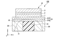
- FIG. 5 is a schematic view of a magnetic memory including a spin orbit torque type magnetization reversal element according to the first to fifth embodiments.
- FIG. 5 is a schematic cross-sectional view of a spin trajectory torque type magnetization reversal element according to Comparative Example 1; It is a graph which shows the examination result of Example 1 and comparative example 1.
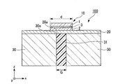
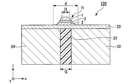
- FIG. 1 is a perspective view schematically showing a spin trajectory torque type magnetization reversal element according to the first embodiment.
- the spin orbit torque type magnetization reversal element 100 according to the first embodiment has a magnetoresistive effect element 10, a spin orbit torque wire 20, and two via wires 30.
- the vertical direction in which the via wire 30 extends from the spin track torque wire 20 is z direction
- the first direction in which the spin track torque wire 20 extends is orthogonal to any of x direction, z direction and x direction Let the direction of 2 be the y direction.
- the magnetoresistance effect element 10 includes a first ferromagnetic metal layer 1 whose magnetization direction is fixed, a second ferromagnetic metal layer 2 whose magnetization direction changes, a first ferromagnetic metal layer 1 and a second ferromagnetic metal layer. And a nonmagnetic layer 3 sandwiched by two.
- the magnetoresistive effect element 10 functions by fixing the magnetization of the first ferromagnetic metal layer 1 in one direction and relatively changing the direction of the magnetization of the second ferromagnetic metal layer 2.
- a coercivity difference type prseudo-spin valve type
- the coercivity of the first ferromagnetic metal layer of the magnetoresistive element is higher than the coercivity of the second ferromagnetic metal layer. Enlarge.
- an exchange bias type spin valve type
- the magnetization of the first ferromagnetic metal layer in the magnetoresistive element is fixed by exchange coupling with the antiferromagnetic layer.
- the magnetoresistive effect element 10 is a tunneling magnetoresistive (TMR) element when the nonmagnetic layer 3 is made of an insulator, and a giant magnetoresistive (GMR) element when the nonmagnetic layer 3 is made of a metal. ) Element.
- TMR tunneling magnetoresistive
- GMR giant magnetoresistive
- the lamination structure of the magnetoresistive effect element can adopt the lamination structure of a well-known magnetoresistive effect element.
- each layer may be composed of a plurality of layers, or may be provided with another layer such as an antiferromagnetic layer for fixing the magnetization direction of the first ferromagnetic metal layer 1.
- the first ferromagnetic metal layer 1 is called a fixed layer or a reference layer
- the second ferromagnetic metal layer 2 is called a free layer or a storage layer.
- a known material can be used as the material of the first ferromagnetic metal layer 1.
- a metal selected from the group consisting of Cr, Mn, Co, Fe and Ni, and an alloy exhibiting one or more of these metals and exhibiting ferromagnetism can be used.
- an alloy containing these metals and at least one or more elements of B, C, and N can also be used.
- Co-Fe and Co-Fe-B can be mentioned.
- Heusler alloy such as Co 2 FeSi.
- the Heusler alloy contains an intermetallic compound having a chemical composition of X 2 YZ, X is a transition metal element or noble metal element of Co, Fe, Ni, or Cu group on the periodic table, and Y is Mn, V Or a transition metal of Cr or Ti group or an element species of X described above, and Z is a typical element of Group III to V group.
- Co 2 FeSi, Co 2 MnSi, Co 2 Mn 1-a Fe a Al b Si 1-b and the like can be mentioned.
- an antiferromagnetic material such as IrMn or PtMn is used as a material in contact with the first ferromagnetic metal layer 1. It is also good. Furthermore, in order to prevent the stray magnetic field of the first ferromagnetic metal layer 1 from affecting the second ferromagnetic metal layer 2, a synthetic ferromagnetic coupling structure may be used.
- the lamination film of Co and Pt in order to make the direction of magnetization of the first ferromagnetic metal layer 1 perpendicular to the lamination surface, it is preferable to use a lamination film of Co and Pt.
- FeB 1.0 nm
- Ta 0.2 nm
- 4 / Ru (0.9 nm) / [Co (0.24 nm) / Pt (0.16 nm)] 6 can be used.
- a ferromagnetic material in particular, a soft magnetic material can be applied.
- a metal selected from the group consisting of Cr, Mn, Co, Fe and Ni, an alloy containing one or more of these metals, and these metals and at least one or more elements of B, C, and N Alloys can be used.
- Co-Fe, Co-Fe-B and Ni-Fe can be mentioned.
- the thickness of the second ferromagnetic metal layer 2 is preferably 2.5 nm or less.
- Perpendicular magnetic anisotropy can be added to the second ferromagnetic metal layer 2 at the interface between the second ferromagnetic metal layer 2 and the nonmagnetic layer 3. Further, since the effect is attenuated by increasing the film thickness of the second ferromagnetic metal layer 2 in the perpendicular magnetic anisotropy, the film thickness of the second ferromagnetic metal layer 2 is preferably smaller.
- Nonmagnetic layer 3 when the nonmagnetic layer 3 is an insulator (when it is a tunnel barrier layer), Al 2 O 3 , SiO 2 , MgO, Ga 2 O 3 , MgAl 2 O 4 or the like may be used as the material. Can. Besides these materials, materials in which a part of Al, Si and Mg is substituted by Zn, Be or the like can also be used. Furthermore, a material in which Mg of MgAl 2 O 4 is substituted by Zn, a material in which Al is substituted by Ga or In, or the like can be used. Among these, MgO and MgAl 2 O 4 have high lattice matching with other layers.
- the nonmagnetic layer 3 is made of metal, Cu, Ag or the like can be used as the material. In addition, alloys such as Ag-Sn and Ag-Mg can also be used. Furthermore, when the nonmagnetic layer 3 is made of a semiconductor, Si, Ge, CuInSe 2 , CuGaSe 2 , Cu (In, Ga) Se 2 or the like can be used as the material.
- the magnetoresistive effect element 10 may have another layer.
- an underlayer may be provided on the surface of the second ferromagnetic metal layer 2 opposite to the nonmagnetic layer 3, or a cap may be provided on the surface of the first ferromagnetic metal layer 1 opposite to the nonmagnetic layer 3. It may have a layer.
- the layer disposed between the spin orbit torque wiring 20 and the magnetoresistive effect element 10 does not dissipate the spins propagating from the spin orbit torque wiring 20.
- the spin orbit torque wiring 20 it is known that silver, copper, magnesium, aluminum, and the like have a long spin diffusion length of 100 nm or more and do not easily dissipate spin.
- the thickness of this layer is preferably equal to or less than the spin diffusion length of the material constituting the layer. If the thickness of the layer is equal to or less than the spin diffusion length, the spins propagating from the spin orbit torque wiring 20 can be sufficiently transmitted to the magnetoresistance effect element 10.
- the spin track torque wiring 20 extends in the x direction.
- the spin orbit torque wiring 20 is connected to one surface of the second ferromagnetic metal layer 2 in the z direction.
- the spin orbit torque wiring 20 may be directly connected to the second ferromagnetic metal layer 2 or may be connected via another layer.
- the spin orbit torque wiring 20 is made of a material in which a pure spin current is generated by the spin Hall effect when current flows.
- a material having a configuration in which a pure spin current is generated in the spin orbit torque wiring 20 is sufficient. Therefore, the material is not limited to a material composed of a single element, and may be composed of a part composed of a material in which a pure spin current is generated and a part composed of a material in which a pure spin current is not generated.
- the spin Hall effect is a phenomenon in which a pure spin current is induced in a direction perpendicular to the direction of the current based on spin-orbit interaction when a current is supplied to a material.
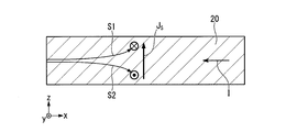
- FIG. 2 is a schematic view for explaining the spin Hall effect.
- FIG. 2 is a cross-sectional view of the spin track torque wiring 20 shown in FIG. 1 cut along the x direction. The mechanism by which a pure spin current is generated by the spin Hall effect will be described based on FIG.
- the first spin S1 oriented to the back of the drawing and the second spin S2 oriented to the front of the drawing are orthogonal to the current. It is bent in the direction.
- the ordinary Hall effect and the spin Hall effect are common in that moving (moving) charges (electrons) can bend the direction of movement (moving), but the ordinary Hall effect causes charged particles moving in a magnetic field to move the Lorentz force.
- the spin Hall effect is largely different in that the direction of movement is bent only by electron movement (only current flow) even though there is no magnetic field.
- the number of electrons in the first spin S1 is equal to the number of electrons in the second spin S2 in a nonmagnetic material (a material that is not a ferromagnetic material)
- the number of electrons in the first spin S1 going upward in the figure and downward
- the number of electrons of the second spin S2 to be directed is equal.
- the current as a net flow of charge is zero.
- a spin current without this current is particularly called a pure spin current.
- the material of the spin orbit torque wiring 20 does not include a material consisting of only a ferromagnetic material.
- J S J ⁇ -J ⁇ .
- J S flows upward in the figure as a pure spin current.
- J S is a current of electrons having a polarizability of 100%.
- the spin orbit torque wiring 20 may contain nonmagnetic heavy metal.
- the heavy metal is used in the meaning of a metal having a specific gravity of yttrium or more.
- the spin orbit torque wiring 20 may be made of only nonmagnetic heavy metal.
- the nonmagnetic heavy metal is preferably a nonmagnetic metal having an atomic number of 39 or more, which has d electrons or f electrons in the outermost shell.
- Such nonmagnetic metals have a large spin-orbit interaction that causes the spin Hall effect.
- the spin orbit torque wiring 20 may be made of only a nonmagnetic metal having a large atomic number of 39 or more, which has d electrons or f electrons in the outermost shell.
- the spin track torque wiring 20 may contain a magnetic metal.
- Magnetic metal refers to ferromagnetic metal or antiferromagnetic metal.
- the spin orbit torque wiring 20 may be made of only an antiferromagnetic metal.
- the spin-orbit interaction is caused by the intrinsic internal field of the material of the spin-orbit torque wiring material, a pure spin current is also generated in the nonmagnetic material.
- the spin current generation efficiency is improved because the magnetic metal itself scatters the electron spins flowing therethrough.
- the addition amount of the magnetic metal is excessively increased, the generated pure spin current is scattered by the added magnetic metal, and as a result, the spin current decreases. Therefore, it is preferable that the molar ratio of the magnetic metal to be added be sufficiently smaller than the molar ratio of the main component of the pure spin generating portion in the spin track torque wiring.
- the molar ratio of the magnetic metal added is preferably 3% or less.
- the spin track torque wiring 20 may also include a topological insulator.
- the spin track torque wire 20 may be made of only the topological insulator.
- the topological insulator is a substance in which the inside of the substance is an insulator or a high resistance, but a spin-polarized metal state is generated on the surface thereof.
- spin-orbit interaction There is something like an internal magnetic field called spin-orbit interaction in matter. Therefore, even if there is no external magnetic field, a new topological phase appears due to the effect of spin-orbit interaction. This is a topological insulator, and strong spin-orbit interaction and inversion symmetry breaking at the edge can generate pure spin current with high efficiency.
- topological insulators example, SnTe, Bi 1.5 Sb 0.5 Te 1.7 Se 1.3, TlBiSe 2, Bi 2 Te 3, Bi 1-x Sb x, (Bi 1-x Sb x) 2 Te 3 and the like are preferred. These topological insulators can generate spin current with high efficiency.
- the via wire 30 extends from the surface of the spin track torque wire 20 opposite to the second ferromagnetic metal layer 2 in the direction intersecting the spin track torque wire 20.
- the spin track torque wiring 20 extends in the vertical direction.
- the end of the via wire 30 opposite to the spin track torque wire 20 is connected to the semiconductor circuit.
- a transistor, a resistive element, a capacitor or the like is connected to the semiconductor circuit to which the via wiring 30 is connected.
- the inter-via distance G in the x direction of the two via wires 30 is shorter than the width d in the x direction of the second ferromagnetic metal layer 2.
- the via wiring 30 and the magnetoresistive effect element 10 overlap when viewed from the z-direction.
- the x-direction and y-direction widths of the via interconnections 30 are designed and can not be freely changed.
- the minimum feature size (F) of the current semiconductor is said to be 7 nm
- the width of the via wiring 30 in the x direction and y direction is at least 7 nm.
- a highly conductive material can be used for the via wiring 30.
- copper, aluminum, silver and the like can be mentioned.
- a nitride film or the like having conductivity can be used.
- the two via wires 30 are insulated by the interlayer insulating portion 31.
- the interlayer insulating portion 31 is an insulating layer which insulates between the wirings and the elements of the multilayer wiring.
- the interlayer insulating portion 31 can be made of the same material as that used in a semiconductor device or the like. For example, silicon oxide (SiO x ), silicon nitride (SiN x ), silicon carbide (SiC), chromium nitride (CrN), silicon carbonitride (SiCN), silicon oxynitride (SiON), aluminum oxide (Al 2 O 3 ) , Zirconium oxide (ZrO x ) or the like is used.
- the Vickers hardness difference between the interlayer insulating portion 31 and the via wiring 30 is preferably 3 GPa or less.
- the polishing state of lamination surface 30a on which spin track torque interconnection 20 is laminated can be made constant by chemical mechanical polishing (CMP) or the like.
- CMP chemical mechanical polishing
- the lamination surface 30 a on which the spin track torque wiring 20 is laminated can be planarized.
- the lamination surface 30a is flattened, the flatness of the lamination surface 20a on which the magnetoresistive effect element 10 is laminated is also enhanced.
- CMP is one of the methods that can use the physical force and the chemical force to polish even if there are different substances in one plane. Therefore, even if the Vickers hardness difference between the interlayer insulating portion 31 and the via wiring 30 is large, the flatness can be enhanced.
- each layer constituting the magnetoresistive element 10 has a thickness of about several nm, and a slight step also affects the characteristics of the magnetoresistive element 10 (for example, the orientation of the magnetization of the magnetoresistive element 10).
- the Vickers hardness difference between the interlayer insulating portion 31 and the via wiring 30 is 3 GPa or less, the generation of a slight level difference that affects the characteristics of the magnetoresistance effect element 10 can also be suppressed.
- At least one of the following first condition or second condition is satisfied as an index of sufficient flatness without a slight level difference.
- the first condition is that the difference in height between the via wiring 30 and the interlayer insulating portion 31 in the z direction is 1.5 nm or less.
- the difference in height position is preferably 1.2 nm or less, more preferably 1.0 nm or less.
- the height position difference between the via wire 30 and the interlayer insulating portion 31 in the z direction is the length of a vertical line from the highest point of the via wire 30 in the z direction to the average surface in the height direction of the interlayer insulating portion 31 means.
- the average surface in the height direction of the interlayer insulating portion 31 means the surface extending to the average height position in the z direction of the interlayer insulating portion 31.
- the second condition is that the convexity obtained by dividing the difference in height position between the via wiring 30 and the interlayer insulating portion 31 in the z direction by the width d of the interlayer insulating portion 31 is 0.015 or less.
- the convexity is preferably 0.012 or less, more preferably 0.010 or less.
- the degree of convexity means the degree of convexity in the protruding direction when the interlayer insulating portion 31 protrudes from the via wire 30, and the degree of convexity in the recessed direction when the interlayer insulating portion 31 is recessed from the via wire 30.
- the following combinations can be considered.
- the interlayer insulating portion 31 is silicon oxide
- vanadium nitride can be used for the via wiring 30.
- the interlayer insulating portion 31 is zirconium oxide
- a nitride containing any one selected from the group consisting of Nb, V and Al can be used for the via wiring 30.
- the interlayer insulating portion 31 is silicon nitride
- a nitride containing any one selected from the group consisting of Nb, Zr, and Al can be used for the via wiring 30.
- a nitride containing Ti or Zr can be used for the via wiring 30.
- the spin orbit torque type magnetization reversal element 100 controls the magnetization direction of the second ferromagnetic metal layer 2 by the spin orbit torque (SOT) induced by the spins injected from the spin orbit torque wiring 20.
- SOT spin orbit torque
- the resistance value of the magnetoresistance effect element 10 changes in accordance with the change in the relative angle between the direction of the magnetization of the first ferromagnetic metal layer 1 and the direction of the magnetization of the second ferromagnetic metal layer 2. Data can be read out by detecting a change in resistance value of the magnetoresistance effect element 10.
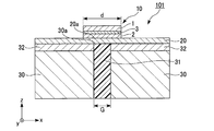
- FIG. 3 is a schematic cross-sectional view of a spin trajectory torque type magnetization reversal element 101 according to the second embodiment.
- the spin orbit torque type magnetization reversal device 101 shown in FIG. 3 is the spin orbit torque type magnetization according to the first embodiment in that the planarizing layer 32 is formed between the spin orbit torque wiring 20 and the via wiring 30. It differs from the inverting element 100.
- the same components as those of the spin orbit torque type magnetization reversal element 100 according to the first embodiment are denoted by the same reference numerals, and the description thereof is omitted.
- the planarization layer 32 has conductivity and is a layer for enhancing the flatness of the laminated surface 30 a on which the spin track torque wiring 20 is laminated.
- a nitride containing any selected from the group consisting of Ti, Nb, V, Ta, Zr and Al can be used. Among these, it is preferable to use a nitride containing Ti or Ta for the planarization layer 32.
- the Vickers hardness difference between the interlayer insulating portion 31 and the planarization layer 32 is preferably 3 GPa or less. By providing the planarization layer 32, the selectivity of the material forming the via wiring 30 can be enhanced. A specific combination in which the Vickers hardness difference between the interlayer insulating portion 31 and the planarizing layer 32 is 3 GPa or less is the same as the relationship between the interlayer insulating portion 31 and the via wiring 30 described above.
- the planarizing layer 32 By enhancing the flatness of the laminated surface 30 a by the planarizing layer 32, it is possible to further suppress the generation of a slight level difference that affects the characteristics of the magnetoresistance effect element 10. Further, the selectivity of the material which can be used for the via wiring 30 is enhanced, and a substance having higher conductivity can be used for the via wiring 30.
- FIG. 4 is a schematic cross-sectional view enlarging the main part of the spin orbit torque type magnetization reversal element 102 according to the third embodiment.
- the spin orbit torque type magnetization reversal element 102 shown in FIG. 4 is different from the spin orbit torque type magnetization reversal element 100 according to the first embodiment in that the spin orbit torque wiring 21 is formed in two layers.
- the same components as those of the spin orbit torque type magnetization reversal element 100 according to the first embodiment are denoted by the same reference numerals, and the description thereof is omitted.
- the spin orbit torque wiring 21 has a layered structure in the z direction.
- the spin track torque wire 21 shown in FIG. 4 includes a first layer 21A on the second ferromagnetic metal layer 2 side and a second layer 21B on the via wire 30 side.
- FIG. 4 illustrates the laminated structure of the spin track torque wiring 21 in two layers, it may be a laminated structure of three or more layers.
- the resistance value of the first layer 21A is lower than the resistance value of the second layer 21B.
- the current tends to flow on the first layer 21A side. Therefore, the current I2 first flows from the via interconnection 30 in the z direction toward the first layer 21A, and then flows in the x direction.
- the spin track torque wiring is a single layer (first embodiment)
- the current I1 flowing through the via wiring 30 and the spin track torque wiring 20 flows in the shortest distance.
- the current I2 has more components in the x direction than the current I1 in the region immediately below the z direction of the magnetoresistance effect element 10.
- the spin Hall effect occurs in the direction orthogonal to the current flow direction. Therefore, when the current I2 has many components in the x direction, spins can be efficiently injected into the second ferromagnetic metal layer 2.
- FIG. 5 is a schematic cross-sectional view of a spin trajectory torque type magnetization reversal element 103 according to the fourth embodiment.
- the spin orbit torque type magnetization reversal element 103 shown in FIG. 5 is characterized in that the cross section of the magnetoresistance effect element 11 is widened from the first ferromagnetic metal layer 1 to the second ferromagnetic metal layer 2. It differs from the spin orbit torque type magnetization reversal element 100 according to the embodiment.
- the same components as those of the spin orbit torque type magnetization reversal element 100 according to the first embodiment are designated by the same reference numerals, and the description thereof will be omitted.
- the cross section of the magnetoresistance effect element 11 is widened from the first ferromagnetic metal layer 1 toward the second ferromagnetic metal layer 2.
- the inter-via distance G in the x direction of the two via wires is shorter than the width d in the x direction of the second ferromagnetic metal layer 2.
- the width d of the second ferromagnetic metal layer 2 in the x direction means the width at the interface with the spin track torque wiring 20.
- the area of the second ferromagnetic metal layer 2 in plan view in the z direction is larger than the area of the first ferromagnetic metal layer 1 in plan view in the z direction. That is, the volume of the second ferromagnetic metal layer 2 is larger than the volume of the first ferromagnetic metal layer 1.
- the magnetization direction of the second ferromagnetic metal layer 2 is more easily changed than the magnetization of the first ferromagnetic metal layer 1.
- the width D in the x direction of the first ferromagnetic metal layer 1 is preferably smaller than the distance G between vias.
- the width D in the x direction of the first ferromagnetic metal layer 1 means the width in the x direction of the first ferromagnetic metal layer 1 on the surface farthest from the spin track torque wiring 20.
- the first ferromagnetic metal layer 1 When the width D in the x direction of the first ferromagnetic metal layer 1 is narrowed, the first ferromagnetic metal layer 1 has a high resistance. That is, part of the current flowing through the spin orbit torque wiring 20 can be prevented from being divided in the stacking direction (z direction) of the magnetoresistive effect element 11. When the x component of the current flowing through the spin orbit torque wiring 20 is increased, the magnetization of the second ferromagnetic metal layer 2 can be more efficiently rotated by SOT.
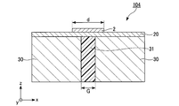
- FIG. 6 is a schematic cross-sectional view of a spin trajectory torque type magnetization reversal element 104 according to the fifth embodiment.
- the spin orbit torque type magnetization reversal element 104 shown in FIG. 6 is different from the spin orbit torque type magnetization reversal element 100 according to the first embodiment in that the nonmagnetic layer 3 and the first ferromagnetic metal layer 1 are not included.
- the same components as those of the spin orbit torque type magnetization reversal element 100 according to the first embodiment are designated by the same reference numerals, and the description thereof will be omitted.
- the spin orbit torque type magnetization reversal element 104 does not have the nonmagnetic layer 3 and the first ferromagnetic metal layer 1.
- the spin orbit torque type magnetization reversal element 104 functions as an element even without these layers.
- it can be used as an AMR (magnetic anisotropy) sensor, or a spatial light modulator using a magnetic Kerr effect or a magnetic Faraday effect.
- the via wiring and the magnetoresistive effect element partially overlap in the z direction. Therefore, the area required for one element can be reduced by the overlapping area, and a plurality of elements can be integrated more efficiently in the integrated circuit. Further, by providing a plurality of spin trajectory torque type magnetization reversal elements according to the first to fifth embodiments, it is possible to obtain the magnetic memory 200 having excellent integration (FIG. 7).
- Example 1 As shown in FIG. 1, a spin orbiting torque type magnetization reversal element 100 was prepared in which the via wire 30 and the magnetoresistance effect element 10 were disposed so as to partially overlap each other as viewed in the z direction.
- the constitutions and thicknesses of the respective layers were set as follows so that the magnetization directions of the first ferromagnetic metal layer 1 and the second ferromagnetic metal layer 2 were in the z direction.
- the planar shape from the z direction of the magnetoresistance effect element 10 is circular, and the diameter d thereof is 100 nm.
- the first ferromagnetic metal layer 1 is made of CoFeB and has a thickness of 1 nm.
- the nonmagnetic layer 3 is made of MgO and has a thickness of 1 nm.
- the second ferromagnetic metal layer 2 is made of CoFeB (1.0 nm) / W (0.15 nm) / [Pt (0.16 nm) / Co (0.16 nm)] 4 / Ru (0.9 nm) / [Co (0) .24 nm) / Pt (0.16 nm)] 6 .
- the spin track torque wiring 20 is made of W, the thickness is 3 nm, and the width in the Y direction is 200 nm.
- the via wiring 30 and the interlayer insulating portion 31 are respectively made of Cu and SiO 2 , and the distance G between the vias is set to 90, 80, 70, 60, and 50 nm.
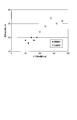
- the reversal current value of the spin orbit torque type magnetization reversal element 100 according to Example 1 was measured.
- the inversion current value and the distance between vias G are shown in Table 1.
- the reversal current was a pulse of 5 nsec, and the write current Iw was applied, and a magnetic field of 50 Oe was applied in the x direction for measurement.
- the direction of magnetization was determined by the magnetoresistance effect caused by flowing the read current Ir in the stacking direction. Therefore, the reversal current value alternately applies the write current Iw and the read current Ir, and after increasing the write current Iw, the reversal current value is estimated from the resistance change obtained from the read current Ir.
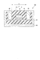
- Comparative example 1 In Comparative Example 1, as shown in FIG. 8, the spin orbit torque type magnetization reversal element 105 in which the via wiring 30 and the magnetoresistance effect element 10 do not overlap in part as viewed from the z direction was manufactured.
- the spin orbit torque type magnetization reversal element 105 shown in FIG. 8 includes a magnetoresistive effect element 10, a spin orbit torque wiring 20, a via wiring 30, an interlayer insulating portion 31, and a semiconductor circuit 40.
- the via wiring 30 connected to the semiconductor circuit 40 is connected to a position different from the magnetoresistive effect element on the same surface as the surface on which the magnetoresistive effect element 10 of the spin track torque wiring 20 is stacked.
- the materials and the like used for the respective components in Comparative Example 1 were the same as in Example 1.
- the distance G between vias is set to 180, 160, 140, 120 and 100 nm
- the spin orbit torque wiring 20 is made of W
- the thickness is 3 nm
- the width in the Y direction is 200 nm.
- the planar shape from the z direction of the magnetoresistance effect element 10 is circular, and the diameter d thereof is 100 nm.
- the reversal current value of the spin orbit torque type magnetization reversal element 100 according to Comparative Example 1 was measured.
- the reversal current value and the distance between vias G are shown in Table 2.
- the reversal current was a pulse of 5 nsec, and the write current Iw was applied, and a magnetic field of 50 Oe was applied in the x direction for measurement.
- the direction of magnetization was determined by the magnetoresistance effect caused by flowing the read current Ir in the stacking direction. Therefore, the reversal current value alternately applies the write current Iw and the read current Ir, and after increasing the write current Iw, the reversal current value is estimated from the resistance change obtained from the read current Ir.
- Example 1 The results of Example 1 and Comparative Example 1 are shown in FIG.
- Example 1 although the via wiring 30 and the magnetoresistive effect element 10 were partially overlapped when viewed from the z direction, a decrease in the reversal current value was observed. Generally, it is considered that magnetization reversal is unlikely to occur because the portion where the via wire 30 and the magnetoresistive element 10 overlap in the z direction has almost no current component in the x direction. Can. However, in FIG. 9, even in the region where the reversal current value and the inter-via distance G are narrower than the length d of the magnetoresistance effect element 10 in the x direction, the reversal current value decreases.
Landscapes
- Engineering & Computer Science (AREA)
- Computer Hardware Design (AREA)
- Hall/Mr Elements (AREA)
- Mram Or Spin Memory Techniques (AREA)
Priority Applications (3)
| Application Number | Priority Date | Filing Date | Title |
|---|---|---|---|
| US16/629,895 US11264563B2 (en) | 2017-09-04 | 2018-08-31 | Spin-orbit-torque magnetization rotational element and magnetic memory |
| CN201880052140.XA CN111052398B (zh) | 2017-09-04 | 2018-08-31 | 自旋轨道转矩型磁化反转元件和磁存储器 |
| US17/578,625 US11832526B2 (en) | 2017-09-04 | 2022-01-19 | Spin-orbit-torque magnetization rotational element and magnetic memory |
Applications Claiming Priority (2)
| Application Number | Priority Date | Filing Date | Title |
|---|---|---|---|
| JP2017169733A JP6686990B2 (ja) | 2017-09-04 | 2017-09-04 | スピン軌道トルク型磁化反転素子及び磁気メモリ |
| JP2017-169733 | 2017-09-04 |
Related Child Applications (2)
| Application Number | Title | Priority Date | Filing Date |
|---|---|---|---|
| US16/629,895 A-371-Of-International US11264563B2 (en) | 2017-09-04 | 2018-08-31 | Spin-orbit-torque magnetization rotational element and magnetic memory |
| US17/578,625 Continuation US11832526B2 (en) | 2017-09-04 | 2022-01-19 | Spin-orbit-torque magnetization rotational element and magnetic memory |
Publications (1)
| Publication Number | Publication Date |
|---|---|
| WO2019045055A1 true WO2019045055A1 (ja) | 2019-03-07 |
Family
ID=65525474
Family Applications (1)
| Application Number | Title | Priority Date | Filing Date |
|---|---|---|---|
| PCT/JP2018/032404 Ceased WO2019045055A1 (ja) | 2017-09-04 | 2018-08-31 | スピン軌道トルク型磁化反転素子及び磁気メモリ |
Country Status (4)
| Country | Link |
|---|---|
| US (2) | US11264563B2 (enExample) |
| JP (1) | JP6686990B2 (enExample) |
| CN (1) | CN111052398B (enExample) |
| WO (1) | WO2019045055A1 (enExample) |
Cited By (3)
| Publication number | Priority date | Publication date | Assignee | Title |
|---|---|---|---|---|
| WO2021212779A1 (zh) * | 2020-04-21 | 2021-10-28 | 浙江驰拓科技有限公司 | 自旋轨道力矩磁存储器件及其制备方法 |
| WO2022102770A1 (ja) * | 2020-11-16 | 2022-05-19 | Tdk株式会社 | 磁化回転素子、磁気抵抗効果素子及び磁気メモリ |
| WO2022220251A1 (ja) * | 2021-04-12 | 2022-10-20 | 国立大学法人東京大学 | 磁気メモリ素子 |
Families Citing this family (5)
| Publication number | Priority date | Publication date | Assignee | Title |
|---|---|---|---|---|
| US11094360B2 (en) * | 2017-10-13 | 2021-08-17 | Semiconductor Energy Laboratory Co., Ltd. | Storage device, electronic component, and electronic device |
| JP6819817B2 (ja) * | 2018-05-31 | 2021-01-27 | Tdk株式会社 | スピン軌道トルク型磁化回転素子、スピン軌道トルク型磁気抵抗効果素子及び磁気メモリ |
| US11895928B2 (en) * | 2019-10-03 | 2024-02-06 | Headway Technologies, Inc. | Integration scheme for three terminal spin-orbit-torque (SOT) switching devices |
| JP2022073039A (ja) * | 2020-10-30 | 2022-05-17 | Tdk株式会社 | スピン素子、磁気アレイ及びスピン素子の製造方法 |
| US12361995B2 (en) | 2022-09-30 | 2025-07-15 | International Business Machines Corporation | Spin-orbit-torque (SOT) MRAM with doubled layer of SOT metal |
Citations (5)
| Publication number | Priority date | Publication date | Assignee | Title |
|---|---|---|---|---|
| WO2016021468A1 (ja) * | 2014-08-08 | 2016-02-11 | 国立大学法人東北大学 | 磁気抵抗効果素子、及び磁気メモリ装置 |
| JP2016046492A (ja) * | 2014-08-26 | 2016-04-04 | ルネサスエレクトロニクス株式会社 | 半導体装置およびその製造方法 |
| JP2017059594A (ja) * | 2015-09-14 | 2017-03-23 | 株式会社東芝 | 磁気メモリ |
| JP2017059634A (ja) * | 2015-09-15 | 2017-03-23 | 株式会社東芝 | 磁気メモリ |
| JP2017059679A (ja) * | 2015-09-16 | 2017-03-23 | 株式会社東芝 | 磁気メモリ |
Family Cites Families (28)
| Publication number | Priority date | Publication date | Assignee | Title |
|---|---|---|---|---|
| JP3377519B2 (ja) * | 2000-12-22 | 2003-02-17 | ティーディーケイ株式会社 | トルクセンサおよびその製造方法 |
| JP4065787B2 (ja) * | 2002-08-30 | 2008-03-26 | 株式会社日立グローバルストレージテクノロジーズ | 磁気ヘッドおよび磁気記録再生装置 |
| JP5382295B2 (ja) | 2008-06-27 | 2014-01-08 | 日本電気株式会社 | 磁気ランダムアクセスメモリ |
| FR2963153B1 (fr) | 2010-07-26 | 2013-04-26 | Centre Nat Rech Scient | Element magnetique inscriptible |
| JP5695453B2 (ja) | 2011-03-07 | 2015-04-08 | ルネサスエレクトロニクス株式会社 | 半導体装置及び半導体装置の製造方法 |
| JP2013016587A (ja) * | 2011-07-01 | 2013-01-24 | Toshiba Corp | 磁気抵抗効果素子及びその製造方法 |
| KR101457511B1 (ko) | 2011-08-18 | 2014-11-04 | 코넬 유니버시티 | 스핀 홀 효과 자기 장치, 방법, 및 적용 |
| JP2013187250A (ja) * | 2012-03-06 | 2013-09-19 | Toshiba Corp | 半導体磁気記憶装置およびその製造方法 |
| JP5605414B2 (ja) | 2012-10-17 | 2014-10-15 | Tdk株式会社 | 電子部品内蔵基板及びその製造方法 |
| WO2017090726A1 (ja) * | 2015-11-27 | 2017-06-01 | Tdk株式会社 | スピン流磁化反転素子、磁気抵抗効果素子及び磁気メモリ |
| KR102515035B1 (ko) * | 2015-12-30 | 2023-03-30 | 에스케이하이닉스 주식회사 | 전자 장치 및 그 제조 방법 |
| JP6833810B2 (ja) | 2016-03-14 | 2021-02-24 | Tdk株式会社 | 磁気メモリ |
| US10686127B2 (en) * | 2016-03-28 | 2020-06-16 | National University Of Singapore | Antiferromagnet and heavy metal multilayer magnetic systems for switching magnetization using spin-orbit torque |
| JP6733496B2 (ja) * | 2016-10-27 | 2020-07-29 | Tdk株式会社 | スピン軌道トルク型磁化反転素子及び磁気メモリ |
| US10396276B2 (en) * | 2016-10-27 | 2019-08-27 | Tdk Corporation | Electric-current-generated magnetic field assist type spin-current-induced magnetization reversal element, magnetoresistance effect element, magnetic memory and high-frequency filter |
| JP2019047120A (ja) * | 2017-09-01 | 2019-03-22 | Tdk株式会社 | スピン流磁化反転素子、スピン軌道トルク型磁気抵抗効果素子、磁気メモリ及び高周波磁気素子 |
| US10741318B2 (en) * | 2017-09-05 | 2020-08-11 | Tdk Corporation | Spin current magnetization rotational element, spin-orbit-torque magnetoresistance effect element, magnetic memory, and high-frequency magnetic element |
| EP3680938B1 (en) * | 2017-09-07 | 2024-11-13 | TDK Corporation | Spin current magnetization reversal element and spin orbit torque type magnetic resistance effect element |
| JP2019057626A (ja) * | 2017-09-21 | 2019-04-11 | Tdk株式会社 | スピン流磁化反転素子、スピン軌道トルク型磁気抵抗効果素子及び磁気メモリ |
| JP7098914B2 (ja) * | 2017-11-14 | 2022-07-12 | Tdk株式会社 | スピン軌道トルク型磁化回転素子、スピン軌道トルク型磁気抵抗効果素子及び磁気メモリ |
| JP6540786B1 (ja) * | 2017-12-28 | 2019-07-10 | Tdk株式会社 | スピン軌道トルク型磁化回転素子、スピン軌道トルク型磁気抵抗効果素子及び磁気メモリ |
| US10971293B2 (en) * | 2017-12-28 | 2021-04-06 | Tdk Corporation | Spin-orbit-torque magnetization rotational element, spin-orbit-torque magnetoresistance effect element, and spin-orbit-torque magnetization rotational element manufacturing method |
| JP7020173B2 (ja) * | 2018-02-26 | 2022-02-16 | Tdk株式会社 | スピン軌道トルク型磁化回転素子、スピン軌道トルク型磁気抵抗効果素子、磁気メモリ及びスピン軌道トルク型磁化回転素子の製造方法 |
| JP7052448B2 (ja) * | 2018-03-16 | 2022-04-12 | Tdk株式会社 | スピン軌道トルク型磁化回転素子、スピン軌道トルク型磁気抵抗効果素子、磁気メモリ及び発振器 |
| JP6919608B2 (ja) * | 2018-03-16 | 2021-08-18 | Tdk株式会社 | スピン軌道トルク型磁化回転素子、スピン軌道トルク型磁気抵抗効果素子及び磁気メモリ |
| JP6819817B2 (ja) * | 2018-05-31 | 2021-01-27 | Tdk株式会社 | スピン軌道トルク型磁化回転素子、スピン軌道トルク型磁気抵抗効果素子及び磁気メモリ |
| JP2020043167A (ja) * | 2018-09-07 | 2020-03-19 | Tdk株式会社 | スピン軌道トルク型磁化回転素子及びスピン軌道トルク型磁気抵抗効果素子 |
| JP2020072199A (ja) * | 2018-10-31 | 2020-05-07 | Tdk株式会社 | スピン軌道トルク型磁化回転素子、スピン軌道トルク型磁気抵抗効果素子及び磁気メモリ |
-
2017
- 2017-09-04 JP JP2017169733A patent/JP6686990B2/ja active Active
-
2018
- 2018-08-31 WO PCT/JP2018/032404 patent/WO2019045055A1/ja not_active Ceased
- 2018-08-31 US US16/629,895 patent/US11264563B2/en active Active
- 2018-08-31 CN CN201880052140.XA patent/CN111052398B/zh active Active
-
2022
- 2022-01-19 US US17/578,625 patent/US11832526B2/en active Active
Patent Citations (5)
| Publication number | Priority date | Publication date | Assignee | Title |
|---|---|---|---|---|
| WO2016021468A1 (ja) * | 2014-08-08 | 2016-02-11 | 国立大学法人東北大学 | 磁気抵抗効果素子、及び磁気メモリ装置 |
| JP2016046492A (ja) * | 2014-08-26 | 2016-04-04 | ルネサスエレクトロニクス株式会社 | 半導体装置およびその製造方法 |
| JP2017059594A (ja) * | 2015-09-14 | 2017-03-23 | 株式会社東芝 | 磁気メモリ |
| JP2017059634A (ja) * | 2015-09-15 | 2017-03-23 | 株式会社東芝 | 磁気メモリ |
| JP2017059679A (ja) * | 2015-09-16 | 2017-03-23 | 株式会社東芝 | 磁気メモリ |
Cited By (6)
| Publication number | Priority date | Publication date | Assignee | Title |
|---|---|---|---|---|
| WO2021212779A1 (zh) * | 2020-04-21 | 2021-10-28 | 浙江驰拓科技有限公司 | 自旋轨道力矩磁存储器件及其制备方法 |
| WO2022102770A1 (ja) * | 2020-11-16 | 2022-05-19 | Tdk株式会社 | 磁化回転素子、磁気抵抗効果素子及び磁気メモリ |
| US12464959B2 (en) | 2020-11-16 | 2025-11-04 | Tdk Corporation | Magnetization rotational element, magnetoresistive effect element, and magnetic memory |
| WO2022220251A1 (ja) * | 2021-04-12 | 2022-10-20 | 国立大学法人東京大学 | 磁気メモリ素子 |
| JPWO2022220251A1 (enExample) * | 2021-04-12 | 2022-10-20 | ||
| JP7710752B2 (ja) | 2021-04-12 | 2025-07-22 | 国立大学法人 東京大学 | 磁気メモリ素子及びその作製方法 |
Also Published As
| Publication number | Publication date |
|---|---|
| US20210083175A1 (en) | 2021-03-18 |
| US20220140231A1 (en) | 2022-05-05 |
| US11832526B2 (en) | 2023-11-28 |
| JP2019047001A (ja) | 2019-03-22 |
| JP6686990B2 (ja) | 2020-04-22 |
| CN111052398A (zh) | 2020-04-21 |
| CN111052398B (zh) | 2023-09-29 |
| US11264563B2 (en) | 2022-03-01 |
Similar Documents
| Publication | Publication Date | Title |
|---|---|---|
| US12048251B2 (en) | Magnetoresistance effect element | |
| US11832526B2 (en) | Spin-orbit-torque magnetization rotational element and magnetic memory | |
| US10665375B2 (en) | Spin current magnetization rotational element, spin-orbit-torque magnetoresistance effect element, magnetic memory, and high-frequency magnetic element | |
| JP2020031234A (ja) | スピン流磁化反転素子 | |
| US11211547B2 (en) | Spin-orbit-torque type magnetization rotating element, spin-orbit-torque type magnetoresistance effect element, and magnetic memory | |
| JP6642773B2 (ja) | スピン流磁化反転素子、スピン軌道トルク型磁気抵抗効果素子、及びスピン流磁化反転素子の製造方法 | |
| CN110914974B (zh) | 自旋轨道转矩型磁化旋转元件、自旋轨道转矩型磁阻效应元件和磁存储器 | |
| JP6540786B1 (ja) | スピン軌道トルク型磁化回転素子、スピン軌道トルク型磁気抵抗効果素子及び磁気メモリ | |
| JPWO2019031226A1 (ja) | スピン流磁気抵抗効果素子及び磁気メモリ | |
| JP2019165244A (ja) | 磁化回転素子、磁気抵抗効果素子及び磁気メモリ | |
| JP2018182256A (ja) | スピン流磁化回転素子、磁気抵抗効果素子及び磁気メモリ | |
| JP6551594B1 (ja) | スピン軌道トルク型磁気抵抗効果素子及び磁気メモリ | |
| JP2019204948A (ja) | スピン軌道トルク型磁化回転素子、スピン軌道トルク型磁気抵抗効果素子及び磁気メモリ | |
| JP2019047110A (ja) | スピン流磁化反転素子、スピン軌道トルク型磁気抵抗効果素子、磁気メモリ及び高周波磁気素子 | |
| WO2020230877A1 (ja) | 磁壁移動素子、磁気記録アレイ及び半導体装置 | |
| CN111279489B (zh) | 自旋轨道转矩型磁阻效应元件及磁存储器 | |
| JP7124788B2 (ja) | スピン流磁化回転型磁気抵抗効果素子、及び磁気メモリ | |
| JP6485588B1 (ja) | データの書き込み方法 | |
| CN114373780A (zh) | 磁畴壁移动元件及磁阵列 | |
| JP2020188138A (ja) | 記憶素子、半導体装置及び磁気記録アレイ | |
| CN115000291A (zh) | 磁器件 | |
| JP6533356B1 (ja) | スピン軌道トルク型磁化回転素子、スピン軌道トルク型磁気抵抗効果素子及び磁気メモリ | |
| WO2023026481A1 (ja) | 磁気抵抗効果素子及び磁気メモリ | |
| CN114914211A (zh) | 磁器件 | |
| WO2024004125A1 (ja) | 磁化回転素子、磁気抵抗効果素子及び磁気メモリ |
Legal Events
| Date | Code | Title | Description |
|---|---|---|---|
| 121 | Ep: the epo has been informed by wipo that ep was designated in this application |
Ref document number: 18851649 Country of ref document: EP Kind code of ref document: A1 |
|
| NENP | Non-entry into the national phase |
Ref country code: DE |
|
| 122 | Ep: pct application non-entry in european phase |
Ref document number: 18851649 Country of ref document: EP Kind code of ref document: A1 |