WO2019044051A1 - プリント配線板の製造方法、プリント配線板、多層プリント配線板の製造方法、及び、多層プリント配線板 - Google Patents
プリント配線板の製造方法、プリント配線板、多層プリント配線板の製造方法、及び、多層プリント配線板 Download PDFInfo
- Publication number
- WO2019044051A1 WO2019044051A1 PCT/JP2018/018706 JP2018018706W WO2019044051A1 WO 2019044051 A1 WO2019044051 A1 WO 2019044051A1 JP 2018018706 W JP2018018706 W JP 2018018706W WO 2019044051 A1 WO2019044051 A1 WO 2019044051A1
- Authority
- WO
- WIPO (PCT)
- Prior art keywords
- resin
- wiring board
- printed wiring
- polymerization initiator
- cured
- Prior art date
- Legal status (The legal status is an assumption and is not a legal conclusion. Google has not performed a legal analysis and makes no representation as to the accuracy of the status listed.)
- Ceased
Links
Images


Classifications
-
- B—PERFORMING OPERATIONS; TRANSPORTING
- B32—LAYERED PRODUCTS
- B32B—LAYERED PRODUCTS, i.e. PRODUCTS BUILT-UP OF STRATA OF FLAT OR NON-FLAT, e.g. CELLULAR OR HONEYCOMB, FORM
- B32B27/00—Layered products comprising a layer of synthetic resin
- B32B27/18—Layered products comprising a layer of synthetic resin characterised by the use of special additives
- B32B27/26—Layered products comprising a layer of synthetic resin characterised by the use of special additives using curing agents
-
- B—PERFORMING OPERATIONS; TRANSPORTING
- B32—LAYERED PRODUCTS
- B32B—LAYERED PRODUCTS, i.e. PRODUCTS BUILT-UP OF STRATA OF FLAT OR NON-FLAT, e.g. CELLULAR OR HONEYCOMB, FORM
- B32B37/00—Methods or apparatus for laminating, e.g. by curing or by ultrasonic bonding
- B32B37/14—Methods or apparatus for laminating, e.g. by curing or by ultrasonic bonding characterised by the properties of the layers
-
- H—ELECTRICITY
- H05—ELECTRIC TECHNIQUES NOT OTHERWISE PROVIDED FOR
- H05K—PRINTED CIRCUITS; CASINGS OR CONSTRUCTIONAL DETAILS OF ELECTRIC APPARATUS; MANUFACTURE OF ASSEMBLAGES OF ELECTRICAL COMPONENTS
- H05K1/00—Printed circuits
- H05K1/02—Details
-
- H—ELECTRICITY
- H05—ELECTRIC TECHNIQUES NOT OTHERWISE PROVIDED FOR
- H05K—PRINTED CIRCUITS; CASINGS OR CONSTRUCTIONAL DETAILS OF ELECTRIC APPARATUS; MANUFACTURE OF ASSEMBLAGES OF ELECTRICAL COMPONENTS
- H05K1/00—Printed circuits
- H05K1/02—Details
- H05K1/03—Use of materials for the substrate
-
- H—ELECTRICITY
- H05—ELECTRIC TECHNIQUES NOT OTHERWISE PROVIDED FOR
- H05K—PRINTED CIRCUITS; CASINGS OR CONSTRUCTIONAL DETAILS OF ELECTRIC APPARATUS; MANUFACTURE OF ASSEMBLAGES OF ELECTRICAL COMPONENTS
- H05K3/00—Apparatus or processes for manufacturing printed circuits
- H05K3/46—Manufacturing multilayer circuits
Definitions
- the present invention relates to a method of manufacturing a printed wiring board, a printed wiring board, a method of manufacturing a multilayer printed wiring board, and a multilayer printed wiring board.
- Printed wiring boards are widely used in electronic devices such as mobile phones, video cameras, notebook computers, etc., to incorporate circuits into complex mechanisms. In recent years, miniaturization of electronic devices has been rapidly promoted. As one of the means for miniaturizing electronic devices, semiconductor components used in electronic devices have been mounted on printed wiring boards with high density. As described above, in order to mount semiconductor components at high density, wiring patterns have been formed at high density also in a printed wiring board. In addition, in order to miniaturize electronic devices, thinning of printed wiring boards has also been performed.
- Patent Document 1 discloses a method of manufacturing a circuit board (flexible printed wiring board) for coping with the high density mounting of the semiconductor component. That is, in Patent Document 1, a first step of forming an insulating layer on a substrate, a first conductive portion on the surface of the insulating layer, and a second conductive portion adjacent to the first conductive portion Forming the first conductive portion and the second conductive portion in a forward tapered shape, and insulating the first conductive portion and the second conductive portion. A third step of press-fitting into a layer, wherein in the third step, a gap is generated between the side surface of the first conductive portion and the second conductive portion and the insulating layer. A method of manufacturing the characterized circuit board is disclosed.
- a printed wiring board When an electronic device (semiconductor component) incorporated in a printed wiring board exhibits a function, heat is also generated at the same time.
- a printed wiring board In order to dissipate the heat, a printed wiring board has been provided with a base material serving as a heat dissipation material on the back side of the position where the electronic device (semiconductor component) is mounted.
- a wiring pattern will be formed on the surface of resin, resin will be hardened after bonding resin and a base material. That is, another process is performed after the wiring pattern is formed on the surface of the resin until the resin is cured. Therefore, there is also a problem that the wiring pattern is shifted before curing the resin.
- the present invention has been made in view of the above problems, and an object of the present invention is to improve the adhesion between a printed wiring board and a substrate such as a heat sink and the adhesion between printed wiring boards.
- a resin laminating step of laminating a first resin in a semi-cured state and a second resin in a semi-cured state A wiring pattern forming step of forming a wiring pattern on the first resin; A first resin curing step of curing the first resin while maintaining the semi-cured state of the second resin; A substrate bonding step of bonding the second resin and the substrate together; And a second resin curing step of curing the second resin and bonding the second resin and the base material,
- the first resin contains a first polymerization initiator
- the second resin is characterized by containing a second polymerization initiator.
- the first resin in the semi-cured state is laminated on the second resin in the semi-cured state.
- a wiring pattern is formed on the first resin, and the second resin and the base are bonded.
- a resin in a semi-cured state means a solid resin having plasticity.
- the first resin in the semi-cured state and the second resin in the semi-cured state are laminated. Therefore, the adhesion between the first resin and the second resin also becomes good.
- the first resin is cured while maintaining the semi-cured state of the second resin. That is, in the method of manufacturing a printed wiring board of the present invention, the first resin is cured before the second resin.
- the wiring pattern formed on the first resin can be sufficiently fixed to the first resin, and the adhesion between the wiring pattern and the first resin can be improved.
- adhesion between the second resin and the substrate is improved. Can. Furthermore, since it is not necessary to use an adhesive separately to bond the substrate, the manufacturing efficiency is improved.
- the base material is a heat dissipation member, the heat generated from the electronic component can be dissipated without an adhesive.
- the wiring pattern in the step of forming a wiring pattern, may be embedded in the first resin after the wiring pattern is formed on the first resin.
- the position of the wiring pattern can be easily fixed, so that the wiring pattern can be prevented from being displaced.
- the substrate bonding step it is desirable to dispose a reinforcing material which can be impregnated with the second resin between the second resin and the substrate.
- a reinforcing material which can be impregnated with the second resin between the second resin and the substrate.
- the strength of the printed wiring board to be manufactured can be strengthened.
- the reinforcing material can be impregnated with the second resin, the second resin and the base material are in direct contact with each other. Therefore, the adhesion between the second resin and the base is unlikely to be inhibited.
- a reinforcing material capable of being impregnated with the first resin and / or the second resin is disposed between the first resin and the second resin. It is desirable to do. By arranging the reinforcing material between the first resin and the second resin, the strength of the printed wiring board to be manufactured can be strengthened. In addition, since the reinforcing material can be impregnated with the first resin and / or the second resin, the first resin and the second resin are in direct contact with each other. Therefore, the adhesion between the first resin and the second resin is not easily inhibited.
- the first polymerization initiator is a photopolymerization initiator
- the second polymerization initiator is a thermal polymerization initiator.
- the first resin may be cured by irradiating the first resin with light
- the second resin may be cured by applying heat to the second resin in the second resin curing step.
- the photopolymerization initiator and the thermal polymerization initiator as the first polymerization initiator and the second polymerization initiator, the first resin is easily cured prior to the curing of the second resin. be able to.
- the first polymerization initiator is a photopolymerization initiator and a thermal polymerization initiator
- the second polymerization initiator is a thermal polymerization initiator
- the first polymerization initiator is used.
- the resin curing step the first resin is cured by irradiating the first resin with light
- the second resin curing step the second resin is cured by applying heat to the second resin.
- heat may be applied to the first resin to cure the first resin.
- the first resin includes the first polymerization initiator including the photopolymerization initiator and the thermal polymerization initiator
- the degree of curing of the first resin can be easily controlled in the first resin curing step.
- heat is also applied to the first resin to cure the second resin, and at the same time, if an uncured portion exists in the first resin, the uncured portion of the first resin The part can be fully cured.
- the first polymerization initiator is a thermal polymerization initiator
- the second polymerization initiator is a photopolymerization initiator
- the first resin may be cured by applying heat to the first resin
- the second resin may be cured by irradiating the second resin with light in the second resin curing step.
- the first polymerization initiator is a thermal polymerization initiator and a photopolymerization initiator
- the second polymerization initiator is a photopolymerization initiator
- the first polymerization initiator is
- the resin curing step the first resin is cured by applying heat to the first resin
- the second resin curing step the second resin is cured by irradiating the second resin with light.
- the first resin may be cured by irradiating the first resin with light.
- the degree of curing of the first resin can be easily controlled in the first resin curing step.
- the first resin is also irradiated with light to cure the second resin, and at the same time, when an uncured portion exists in the first resin, the first resin The uncured portion of the resin can be sufficiently cured.
- the base material is translucent.
- the second resin curing step it is desirable that the second resin be cured by irradiating the second resin with light from at least the substrate side.
- the substrate has translucency, light emitted from the substrate side can also reach the second resin. Therefore, the second resin can be cured efficiently.
- the first polymerization initiator is a thermal polymerization initiator
- the second polymerization initiator is a thermal polymerization initiator
- the temperature at which the second resin remains in a semi-cured state, and heat at a temperature at which the first resin cures is applied to cure the first resin
- Heat of a temperature at which the second resin cures may be added to cure the second resin. That is, by adjusting the composition of the first resin and the second resin so that the curing temperature of the first resin is lower than the curing temperature of the second resin, the curing time of the first resin and the curing of the second resin You may stagger the time.
- the first resin can be cured without completely curing the second resin.
- the position of the wiring pattern formed in the first resin can be easily fixed, so that the wiring pattern can be prevented from being displaced.
- the second resin is not completely cured in the first resin curing step, the adhesion to the substrate is improved.
- the 10-hour half-life temperature of the first polymerization initiator is lower than the 10-hour half-life temperature of the second polymerization initiator, and in the first resin curing step, The first resin is cured by applying heat to the first resin at a temperature lower than the 10-hour half-life temperature of the second polymerization initiator, and in the second resin curing step, the second polymerization initiation
- the second resin may be cured by applying heat to the second resin at a temperature above the 10 hour half-life temperature of the agent.
- the second heat treatment can be easily performed by controlling the temperature of heat in the first resin curing step and the second resin curing step.
- the curing of the first resin can be performed prior to the curing of the resin.
- the first polymerization initiator is a photopolymerization initiator
- the second polymerization initiator is a photopolymerization initiator
- the substrate has a light transmitting property.
- the first resin and the second resin are laminated with the light impermeable layer interposed between the first resin and the second resin, and the first resin is laminated.
- the first resin is cured by irradiating the first resin with light from the first resin side
- the second resin curing step light is applied to the second resin from the substrate side.
- the second resin may be cured by irradiation.
- the first resin when the light impermeable layer is interposed between the first resin and the second resin, when the light is irradiated from the first resin side, the light does not reach the second resin. Therefore, by adjusting the light irradiation direction, the first resin can be easily cured prior to the curing of the second resin.
- the first polymerization initiator functions as a photopolymerization initiator by being irradiated with light of the first wavelength
- the second polymerization initiator has the second wavelength.
- the first wavelength and the second wavelength are different wavelengths
- the semi-cured state of the second resin is While maintaining, the first resin is irradiated with the light of the first wavelength to cure the first resin
- the second resin is irradiated with the light of the second wavelength.
- the second resin may be cured.
- the base material has translucency
- the second resin curing step the second resin is irradiated with light of the second wavelength from at least the base side. It is desirable to cure the said 2nd resin by carrying out.
- the substrate has translucency
- the light of the second wavelength irradiated from the substrate side can also reach the second resin. Therefore, the second resin can be cured efficiently.
- the above-mentioned resin laminating step, the above-mentioned wiring pattern forming step, the above first resin curing step, the above substrate bonding step and the above second resin curing step It is desirable to do it continuously. By continuously performing these steps with a roll press, a printed wiring board can be efficiently manufactured.
- the printed wiring board of the present invention is A first cured resin layer having a wiring pattern formed on one side thereof, A second cured resin layer laminated on the surface of the first cured resin layer opposite to the surface on which the wiring pattern is formed; A printed wiring board comprising: a base material adhered to the surface of the second cured resin layer opposite to the surface in contact with the first cured resin layer;
- the first cured resin layer is a cured resin in which a first resin is cured by a first polymerization initiator,
- the second cured resin layer is a cured resin obtained by curing a second resin with a second polymerization initiator,
- the first curing means for curing the first resin with the first polymerization initiator is different from the second means for curing the second resin with the second polymerization initiator.
- the printed wiring board having such a configuration is a printed wiring board manufactured by the method for manufacturing a printed wiring board of the present invention. Therefore, in the printed wiring board of such a configuration, the adhesion between the second
- the wiring pattern is preferably embedded in the first cured resin layer.
- the wiring pattern is unlikely to be deviated.
- the method for producing a multilayer printed wiring board of the present invention is A method for producing a multilayer printed wiring board, comprising: laminating an upper layer printed wiring board and a lower layer printed wiring board to produce a multilayer printed wiring board, A resin laminating step for the upper layer printed wiring board, wherein the first resin in the semi-cured state and the second resin in the semi-cured state are laminated; A first wiring pattern forming step of forming a first wiring pattern in the first resin; A first resin curing step of curing an upper printed wiring board by curing the first resin while maintaining a semi-cured state of the second resin; A lower layer printed wiring board preparing step of preparing a lower layer printed wiring board in which a second wiring pattern is formed in a third resin; A printed wiring board laminating step of laminating the lower layer printed wiring board under the upper layer printed wiring board; And a second resin curing step of curing the second resin and bonding the upper layer printed wiring board and the lower layer printed wiring board.
- the first resin contains a first polymerization initi
- the first resin in the semi-cured state is laminated on the second resin in the semi-cured state.
- a step after the method for manufacturing a multilayer printed wiring board of the present invention a first wiring pattern is formed on the first resin, and the second resin and the lower layer printed wiring board are bonded.
- Manufactured by using a resin of a type that improves the transmission characteristics of the first wiring pattern as the first resin, and using a type of resin that improves the adhesion with the lower layer printed wiring board as the second resin In a multilayer printed wiring board, transmission characteristics and adhesion between the printed wiring boards can be compatible.
- the first resin in the semi-cured state and the second resin in the semi-cured state are laminated. Therefore, the adhesion between the first resin and the second resin also becomes good.
- the first resin is cured while maintaining the semi-cured state of the second resin. That is, in the method for manufacturing a multilayer printed wiring board of the present invention, the first resin is cured before the second resin.
- the first resin is cured before the second resin.
- the second resin in a semi-cured state and the third resin of the lower layer printed wiring board are adhered after curing of the first resin, the second resin and the lower layer printed wiring The adhesion of the plate to the third resin can be improved.
- the second resin is cured in a state in which the adhesion between the second resin and the third resin is high, so the upper layer printed wiring board and the lower layer printed wiring board are strong. It will be glued to
- the upper layer printed wiring is electrically connected such that the first wiring pattern and the second wiring pattern are electrically connected via the conductive member. It is desirable to laminate a board and a lower layer printed wiring board. As described above, by manufacturing a multilayer printed wiring board, the wiring pattern can be made high in density.
- the first polymerization initiator is a photopolymerization initiator
- the second polymerization initiator is a thermal polymerization initiator
- the first resin may be cured by irradiating the first resin with light
- the second resin may be cured by applying heat to the second resin.
- the first polymerization initiator is a photopolymerization initiator and a thermal polymerization initiator
- the second polymerization initiator is a thermal polymerization initiator
- the first polymerization initiator is a heat polymerization initiator.
- the first resin is cured by irradiating the first resin with light
- the second resin is cured by applying heat to the second resin.
- the first resin may be cured by applying heat to the first resin.
- the degree of curing of the first resin can be easily controlled in the first resin curing step.
- heat is also applied to the first resin to cure the second resin, and at the same time, if an uncured portion exists in the first resin, the uncured portion of the first resin The part can be fully cured.
- the first polymerization initiator is a thermal polymerization initiator
- the second polymerization initiator is a photopolymerization initiator
- the first resin may be cured by applying heat to the first resin
- the second resin may be cured by irradiating the second resin with light in the second resin curing step.
- the first polymerization initiator is a thermal polymerization initiator and a photopolymerization initiator
- the second polymerization initiator is a photopolymerization initiator
- the first polymerization initiator is a photopolymerization initiator.
- the first resin curing step the first resin is cured by applying heat to the first resin
- the second resin curing step the second resin is irradiated by irradiating the second resin with light.
- the first resin may be cured by irradiating the first resin with light.
- the degree of curing of the first resin can be easily controlled in the first resin curing step.
- the first resin is also irradiated with light to cure the second resin, and at the same time, when an uncured portion exists in the first resin, the first resin The uncured portion of the resin can be sufficiently cured.
- the first polymerization initiator is a thermal polymerization initiator
- the second polymerization initiator is a thermal polymerization initiator
- the heat of the temperature at which the second resin cures may be applied to cure the second resin. That is, by adjusting the composition of the first resin and the second resin so that the curing temperature of the first resin is lower than the curing temperature of the second resin, the curing time of the first resin and the curing of the second resin You may stagger the time.
- the first resin can be cured without completely curing the second resin in this case.
- the position of the wiring pattern formed in the first resin can be easily fixed, so that the wiring pattern can be prevented from being displaced.
- the second resin is not completely cured in the first resin curing step, the adhesion to the substrate is improved.
- the 10-hour half-life temperature of the first polymerization initiator is lower than the 10-hour half-life temperature of the second polymerization initiator, and in the first resin curing step Heat is applied to the first resin at a temperature lower than a 10-hour half-life temperature of the second polymerization initiator to cure the first resin, and in the second resin curing step, the second polymerization is performed
- the second resin may be cured by applying heat to the second resin at a temperature above the 10 hour half-life temperature of the initiator.
- the second heat treatment can be easily performed by controlling the temperature of heat in the first resin curing step and the second resin curing step.
- the curing of the first resin can be performed prior to the curing of the resin.
- the first polymerization initiator functions as a photopolymerization initiator by being irradiated with light of a first wavelength
- the second polymerization initiator has a second wavelength.
- the first wavelength and the second wavelength are different wavelengths by being irradiated with the light of the second wavelength, and in the first resin curing step, the semi-cured state of the second resin While maintaining the above, the first resin is irradiated with the light of the first wavelength to cure the first resin, and in the second resin curing step, the second resin is irradiated with the light of the second wavelength.
- the second resin may be cured by carrying out.
- the second wiring pattern is formed on the third resin in a semi-cured state containing a third polymerization initiator, and then the second wiring pattern is formed.
- the third resin is cured so that the resin is not completely cured to produce the lower layer printed wiring board, and in the second resin curing step, the second resin is cured and the third resin is simultaneously cured. It is desirable that the upper layer printed wiring board and the lower layer printed wiring board be adhered after completely curing.
- the second wiring pattern is formed on the third resin in the semi-cured state, and then the third resin is cured to prevent the third resin from being completely cured, thereby forming the third resin.
- the second wiring pattern can be sufficiently fixed to the third resin, and the adhesion between the second wiring pattern and the third resin can be improved. Moreover, in the method of manufacturing such a multilayer printed wiring board, since the second resin in the semi-cured state and the third resin in the semi-cured state are laminated, the upper layer printed wiring board and the lower layer printed wiring board The adhesion of the above can be improved.
- the third resin in a semi-cured state containing a third polymerization initiator, and the third in a semi-cured state containing a fourth polymerization initiator (4)
- the resin is laminated, the second wiring pattern is formed on the third resin, and then the third resin is cured while maintaining the semi-cured state of the fourth resin to produce a lower layer printed wiring board
- the fourth resin may also be cured.
- the third polymerization initiator may be a thermal polymerization initiator or a photopolymerization initiator.
- the multilayer printed wiring board of the present invention is A multilayer printed wiring board in which an upper layer printed wiring board on which a first wiring pattern is formed and a lower layer printed wiring board on which a second wiring pattern is formed on a third resin are laminated,
- the upper layer printed wiring board has a first cured resin layer having the first wiring pattern formed on one surface thereof; And a second cured resin layer laminated on the surface of the first cured resin layer opposite to the surface on which the first wiring pattern is formed,
- the first cured resin layer is a cured resin in which a first resin is cured by a first polymerization initiator,
- the second cured resin layer is a cured resin obtained by curing a second resin with a second polymerization initiator,
- the first curing means for curing the first resin with the first polymerization initiator is different from the second means for curing the second resin with the second polymerization initiator.
- the multilayer printed wiring board of such a configuration is a printed wiring board manufactured by the method for manufacturing a multilayer printed wiring board of the present invention. Therefore, in the multilayer printed wiring board of such a configuration, the adhesion between the upper layer printed wiring board and the lower layer printed wiring board is sufficiently high.
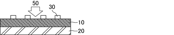
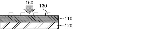
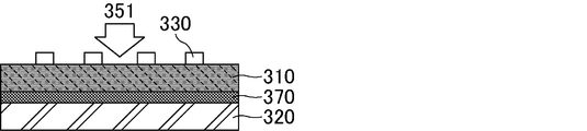
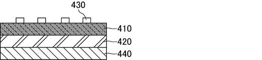
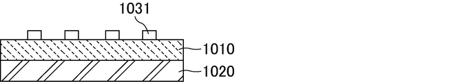
- FIG. 1 is a schematic diagram which shows typically an example of the lamination process in the manufacturing method of the printed wiring board which concerns on 1st Embodiment of this invention.
- FIG. 2 is a schematic diagram which shows typically an example of the wiring pattern formation process in the manufacturing method of the printed wiring board which concerns on 1st Embodiment of this invention.
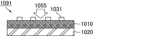
- FIG. 3 is a schematic diagram which shows typically an example of the 1st resin hardening process in the manufacturing method of the printed wiring board which concerns on 1st Embodiment of this invention.
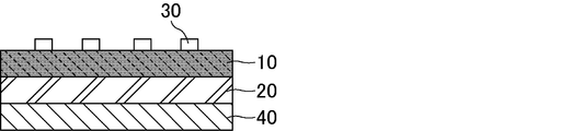
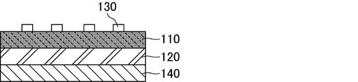
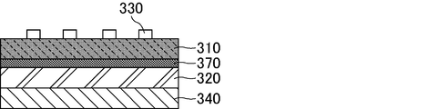
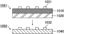
- FIG. 4 is a schematic diagram which shows typically an example of the base-material bonding process in the manufacturing method of the printed wiring board which concerns on 1st Embodiment of this invention.
- FIG. 1 is a schematic diagram which shows typically an example of the lamination process in the manufacturing method of the printed wiring board which concerns on 1st Embodiment of this invention.
- FIG. 2 is a schematic diagram which shows typically an example of the wiring pattern formation process in the manufacturing method of the printed wiring board which concerns
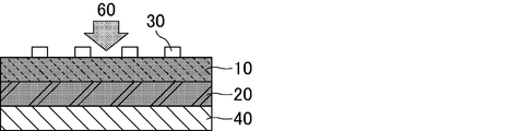
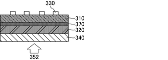
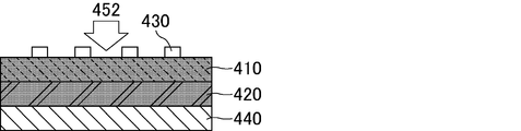
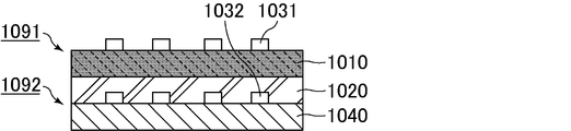
- FIG. 5 is a schematic diagram which shows typically an example of the 2nd resin hardening process in the manufacturing method of the printed wiring board which concerns on 1st Embodiment of this invention.
- FIG. 6 is a schematic diagram which shows typically an example of the lamination process in the manufacturing method of the printed wiring board which concerns on 2nd Embodiment of this invention.
- FIG. 7 is a schematic diagram which shows typically an example of the wiring pattern formation process in the manufacturing method of the printed wiring board which concerns on 2nd Embodiment of this invention.
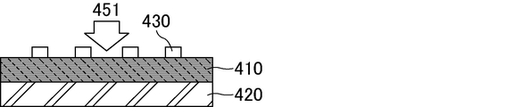
- FIG. 8 is a schematic diagram which shows typically an example of the 1st resin hardening process in the manufacturing method of the printed wiring board which concerns on 2nd Embodiment of this invention.
- FIG. 6 is a schematic diagram which shows typically an example of the lamination process in the manufacturing method of the printed wiring board which concerns on 2nd Embodiment of this invention.
- FIG. 7 is a schematic diagram which shows typically an example of the wiring pattern formation process in the manufacturing method of the printed wiring board which concerns on 2nd
- FIG. 9 is a schematic diagram which shows typically an example of the base-material bonding process in the manufacturing method of the printed wiring board which concerns on 2nd Embodiment of this invention.
- FIG. 10 is a schematic view schematically showing an example of a second resin curing step in the method for manufacturing a printed wiring board according to the second embodiment of the present invention.
- FIG. 11 is a schematic diagram which shows typically an example of the lamination process in the manufacturing method of the printed wiring board which concerns on 3rd Embodiment of this invention.
- FIG. 12 is a schematic diagram which shows typically an example of the wiring pattern formation process in the manufacturing method of the printed wiring board which concerns on 3rd Embodiment of this invention.
- FIG. 13 is a schematic diagram which shows typically an example of the 1st resin hardening process in the manufacturing method of the printed wiring board which concerns on 3rd Embodiment of this invention.
- FIG. 14 is a schematic diagram which shows typically an example of the base-material bonding process in the manufacturing method of the printed wiring board which concerns on 3rd Embodiment of this invention.
- FIG. 15 is a schematic diagram which shows typically an example of the 2nd resin hardening process in the manufacturing method of the printed wiring board which concerns on 3rd Embodiment of this invention.
- FIG. 16 is a schematic diagram which shows typically an example of the lamination process in the manufacturing method of the printed wiring board which concerns on 4th Embodiment of this invention.
- FIG. 17 is a schematic diagram which shows typically an example of the wiring pattern formation process in the manufacturing method of the printed wiring board which concerns on 4th Embodiment of this invention.
- FIG. 18 is a schematic view schematically showing an example of a first resin curing step in the method for manufacturing a printed wiring board according to the fourth embodiment of the present invention.
- FIG. 19 is a schematic diagram which shows typically an example of the base-material bonding process in the manufacturing method of the printed wiring board which concerns on 4th Embodiment of this invention.
- FIG. 20 is a schematic view schematically showing an example of a second resin curing step in the method for manufacturing a printed wiring board according to the fourth embodiment of the present invention.
- FIG. 21 is a schematic diagram which shows typically an example of the lamination process in the manufacturing method of the printed wiring board which concerns on 5th Embodiment of this invention.
- FIG. 22 is a schematic diagram which shows typically an example of the wiring pattern formation process in the manufacturing method of the printed wiring board which concerns on 5th Embodiment of this invention.
- FIG. 23 is a schematic diagram which shows typically an example of the 1st resin hardening process in the manufacturing method of the printed wiring board which concerns on 5th Embodiment of this invention.
- FIG. 24 is a schematic diagram which shows typically an example of the base-material bonding process in the manufacturing method of the printed wiring board which concerns on 5th Embodiment of this invention.
- FIG. 25 is a schematic diagram which shows typically an example of the 2nd resin hardening process in the manufacturing method of the printed wiring board which concerns on 5th Embodiment of this invention.
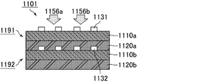
- 26 (a) to 26 (e) are schematic views schematically showing an example of a method of manufacturing a printed wiring board according to a sixth embodiment of the present invention in the order of steps.
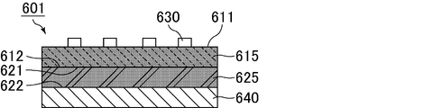
- FIG. 27 is a schematic view schematically showing an example of the printed wiring board of the present invention.
- FIG. 28: is process drawing which shows typically an example of the resin lamination process for upper layer printed wiring boards in the manufacturing method of the multilayer printed wiring board which concerns on 8th Embodiment of this invention.
- FIG. 29 is a process chart schematically showing an example of a first wiring pattern forming step in the method for manufacturing a multilayer printed wiring board according to the eighth embodiment of the present invention.
- FIG. 30 is process drawing which shows typically an example of the 1st resin hardening process in the manufacturing method of the multilayer printed wiring board which concerns on 8th Embodiment of this invention.
- FIG. 31 is a process chart schematically showing an example of a lower layer printed wiring board preparing step in the method for manufacturing a multilayer printed wiring board according to the eighth embodiment of the present invention.
- FIG. 32: is process drawing which shows typically an example of the printed wiring board lamination
- FIG. 33 is process drawing which shows typically an example of the 2nd resin hardening process in the manufacturing method of the multilayer printed wiring board which concerns on 8th Embodiment of this invention.
- 34 (a) and 34 (b) are schematic views schematically showing an example of a printed wiring board laminating step in the method for manufacturing a multilayer printed wiring board according to the ninth embodiment of the present invention.
- FIG. 35 is process drawing which shows typically an example of the resin lamination process for printed wiring boards in the manufacturing method of the multilayer printed wiring board which concerns on 11th Embodiment of this invention.
- FIG. 36 is a process diagram schematically showing an example of a wiring pattern forming step in the method for manufacturing a multilayer printed wiring board according to the eleventh embodiment of the present invention.
- FIG. 37 is a process diagram schematically showing an example of a first resin curing step in the method for manufacturing a multilayer printed wiring board according to the eleventh embodiment of the present invention.
- FIG. 38 is a process chart schematically showing one example of a printed wiring board laminating step in the method for manufacturing a multilayer printed wiring board according to the eleventh embodiment of the present invention.
- FIG. 39 is a process diagram schematically showing an example of a second resin curing step in the method for manufacturing a multilayer printed wiring board according to the eleventh embodiment of the present invention.
- the first resin in the semi-cured state and the second resin in the semi-cured state are laminated (1) a resin laminating step, and a wiring pattern is formed on the first resin (2 )
- the first resin is cured while maintaining the wiring pattern formation step and the semi-cured state of the second resin (3)
- the first resin curing step, and the second resin and the base material are bonded together (4)
- a material bonding step, and (5) a second resin curing step of curing the second resin and bonding the second resin and the base material are included.
- the first resin contains a first polymerization initiator
- the second resin contains a second polymerization initiator.
- the first resin in the semi-cured state and the second resin in the semi-cured state are laminated.
- a wiring pattern is formed on the first resin, and the second resin and the base are bonded.
- the first resin in the semi-cured state is laminated on the second resin in the semi-cured state. Therefore, when the first resin and the second resin are in direct contact with each other, the adhesion between the first resin and the second resin becomes good. In addition, when another layer is sandwiched between the first resin and the second resin, the adhesion between the other layer and the first resin and the second resin is improved.
- the first resin is cured while maintaining the semi-cured state of the second resin. That is, in the method of manufacturing a printed wiring board of the present invention, the first resin is cured before the second resin.
- the wiring pattern formed on the first resin can be sufficiently fixed to the first resin, and the adhesion between the wiring pattern and the first resin can be improved.
- adhesion between the second resin and the substrate is improved. Can. Furthermore, since it is not necessary to use an adhesive separately to bond the substrate, the manufacturing efficiency is improved.
- the method for producing a printed wiring board according to the first embodiment of the present invention includes (1) resin laminating step to (5) second resin curing step, and the first polymerization initiator is a photopolymerization initiator.
- the second polymerization initiator is a thermal polymerization initiator.
- the first resin is cured by irradiating the first resin with light
- (5) in the second resin curing step heat is applied to the second resin.
- the second resin is cured.
- FIG. 1 is a schematic diagram which shows typically an example of the lamination process in the manufacturing method of the printed wiring board which concerns on 1st Embodiment of this invention.
- FIG. 2 is a schematic diagram which shows typically an example of the wiring pattern formation process in the manufacturing method of the printed wiring board which concerns on 1st Embodiment of this invention.
- FIG. 3 is a schematic diagram which shows typically an example of the 1st resin hardening process in the manufacturing method of the printed wiring board which concerns on 1st Embodiment of this invention.
- FIG. 1 is a schematic diagram which shows typically an example of the lamination process in the manufacturing method of the printed wiring board which concerns on 1st Embodiment of this invention.
- FIG. 2 is a schematic diagram which shows typically an example of the wiring pattern formation process in the manufacturing method of the printed wiring board which concerns on 1st Embodiment of this invention.
- FIG. 3 is a schematic diagram which shows typically an example of the 1st resin hardening process in the manufacturing method of the printed wiring board
- FIG. 4 is a schematic diagram which shows typically an example of the base-material bonding process in the manufacturing method of the printed wiring board which concerns on 1st Embodiment of this invention.
- FIG. 5 is a schematic diagram which shows typically an example of the 2nd resin hardening process in the manufacturing method of the printed wiring board which concerns on 1st Embodiment of this invention.
- the material of the first resin 10 is not particularly limited, it is desirable that the material is a photocurable resin or a thermosetting resin.
- examples of such resin include phenol resin, polyester resin, polyimide resin, polysulfonic acid resin, polyetherimide resin, polyether ketone resin, polycarbonate resin, polyurethane resin, polysiloxane resin, polyamide resin and the like.
- polyimide resins are preferable.
- the polyimide resin is preferably a curable resin composition containing (A) a bismaleimide compound represented by the following general formula (1).
- X is an aliphatic, alicyclic or aromatic hydrocarbon group and is a hydrocarbon group having 10 to 30 carbon atoms in its main chain, and these groups are hetero compounds It may have an atom, a substituent or a siloxane skeleton.
- X is preferably an aliphatic or alicyclic hydrocarbon or an aliphatic hydrocarbon group modified by an alicyclic hydrocarbon group, and more preferably an aliphatic hydrocarbon group having 10 to 55 carbon atoms. And 10 to 40 carbon atoms are more preferable.
- Y represents an aliphatic, alicyclic or aromatic hydrocarbon group, and these groups have a hetero atom, a substituent, a phenyl ether skeleton, a sulfonyl skeleton or a siloxane skeleton It is also good.
- Y is preferably an aromatic hydrocarbon group.
- n is the number of repeating units and represents a number in the range of 1 to 20.
- a wiring pattern is formed on the first resin 10.
- the material of the first resin 10 is the above-described resin, the transmission characteristics of the signal transmitted in the wiring pattern are improved.
- the thickness of the first resin 10 is not particularly limited, but is preferably 5 to 100 ⁇ m, and more preferably 10 to 100 ⁇ m. If the thickness of the first resin 10 is less than 5 ⁇ m, the strength of the printed wiring board tends to be weak. When the thickness of the first resin 10 exceeds 100 ⁇ m, the printed wiring board becomes thick, which makes it difficult to miniaturize the electronic device.
- the relative dielectric constant of the first resin 10 is desirably 2 to 3 at a frequency of 1 GHz.
- the dielectric loss tangent of the first resin 10 is preferably 0.0001 to 0.002 at a frequency of 1 GHz.
- the first resin 10 contains a first polymerization initiator which is a photopolymerization initiator.
- the first polymerization initiator is not particularly limited as long as it is a photopolymerization initiator, and for example, an alkylphenone photopolymerization initiator, an acylphosphine photopolymerization initiator, an oxime ester photopolymerization initiator, a thioxanthone type Photopolymerization initiators can be mentioned.
- acetophenone 2,2-dimethoxyacetophenone, p-dimethylaminoacetophenone, Michler's ketone, benzyl, benzoin, benzoin methyl ether, benzoin ethyl ether, benzoin isopropyl ether, benzoin n-propyl ether, benzoin isopropyl ether, benzoin n -Butyl ether, benzyl dimethyl ketal, thioxaton, 2-chlorothioxasone, 2-methylthioxaton, 2,2-dimethoxy-1,2-diphenylethan-1-one, 1-hydroxy-cyclohexyl-phenyl-ketone, 2 -Hydroxy-2-methyl-1-phenyl-propan-1-one, 1- [4- (2-hydroxyethoxy) -phenyl] -2-hydroxy-2-methyl-1-propane-1 One, 2-hydroxy-1- ⁇ 4- [4- (2-hydroxye
- a photopolymerization initiator that efficiently generates radicals at an exposure wavelength of 310 to 436 nm, more preferably at an exposure wavelength of 310 to 365 nm, is desirable.
- 1,2-octanedione having an oxime structure 1- [4- (phenylthio) -2- (O-benzoyloxime)] (manufactured by BASF Japan Ltd., “IRGACURE OXE” -01 "), Ethanone, 1- [9-ethyl-6- (2-methylbenzoyl) -9H-carbazol-3-yl] -1- (O-acetyloxime) (manufactured by BASF Japan Ltd.,“ IRGACURE OXE- 02 ′ ′), 2,4-dimethylthioxanthone having a thioxanthone structure (manufactured by Nippon Kayaku Co.,
- the first polymerization initiator may be composed of one kind of the above-mentioned photopolymerization initiator, or may be composed of two or more kinds.
- the material of the second resin 20 is not particularly limited, for example, it is desirable that the material is a photocurable resin or a thermosetting resin.
- examples of such resin include phenol resin, polyester resin, polyimide resin, polysulfonic acid resin, polyetherimide resin, polyether ketone resin, polycarbonate resin, polyurethane resin, polysiloxane resin, polyamide resin and the like.
- polyimide resins are preferable.
- the polyimide resin is preferably a curable resin composition containing (A) a bismaleimide compound represented by the following general formula (1).
- X is an aliphatic, alicyclic or aromatic hydrocarbon group and is a hydrocarbon group having 10 to 30 carbon atoms in its main chain, and these groups are hetero compounds It may have an atom, a substituent or a siloxane skeleton.
- X is preferably an aliphatic or alicyclic hydrocarbon or an aliphatic hydrocarbon group modified by an alicyclic hydrocarbon group, and more preferably an aliphatic hydrocarbon group having 10 to 55 carbon atoms. And 10 to 40 carbon atoms are more preferable.
- Y represents an aliphatic, alicyclic or aromatic hydrocarbon group, and these groups have a hetero atom, a substituent, a phenyl ether skeleton, a sulfonyl skeleton or a siloxane skeleton It is also good.
- Y is preferably an aromatic hydrocarbon group.
- n is the number of repeating units and represents a number in the range of 1 to 20.
- the second resin 20 is adhered to the base material.
- the adhesiveness with a base material improves that the material of 2nd resin 20 is the said resin.
- the thickness of the second resin 20 is not particularly limited, but is preferably 5 to 100 ⁇ m, and more preferably 10 to 100 ⁇ m. If the thickness of the second resin 20 is less than 5 ⁇ m, the strength of the printed wiring board tends to be weak. When the thickness of the second resin 20 exceeds 100 ⁇ m, the printed wiring board becomes thick, which makes it difficult to miniaturize the electronic device.
- the second resin 20 may contain a functional material such as a thermally conductive filler or a flame retardant.
- a heat conductive filler copper particles, copper coating resin particles, boron nitride, aluminum nitride, alumina, alumina hydrate, silicon oxide, silicon nitride, silicon carbide, diamond, hydroxyapatite, barium titanate, aluminum, silica, Examples include magnesia, titania, silicon nitride, silicon carbide and the like.
- the flame retardant include bromine flame retardants, phosphorus flame retardants, nitrogen flame retardants, silicone flame retardants, inorganic flame retardants, organic metal salt flame retardants and the like.
- brominated flame retardants include polybrominated diphenyl oxide, decabromodiphenyl oxide, tris [3-bromo-2,2-bis (bromomethyl) propyl] phosphate, tris (2,3-dibromopropyl) phosphate, tetrabromo Phthalic acid, bis (2,3-dibromopropyl ether) of tetrabromobisphenol A, brominated epoxy resin, ethylene-bis (tetrabromophthalimide), octabromodiphenyl ether, 1,2-bis (tribromophenoxy) ethane, tetrabromo And -bisphenol A, ethylene bis- (dibromo-norbornane dicarboximide), tris- (2,3-dibromopropyl) -isocyanurate, ethylene-bis-tetrabromophthalimide and the like.
- inorganic phosphorus flame retardant As a phosphorus flame retardant, both an inorganic phosphorus flame retardant and an organic phosphorus flame retardant can be used.
- inorganic phosphorus-based flame retardant compounds include inorganic phosphorus-containing phosphorus such as red phosphorus, monoammonium phosphate, diammonium phosphate, ammonium triphosphate, ammonium polyphosphate such as ammonium polyphosphate, and phosphoric acid amide. Compounds are mentioned.
- Red phosphorus is preferably surface-treated for the purpose of preventing hydrolysis etc.
- the surface treatment method is (i) magnesium hydroxide, aluminum hydroxide, zinc hydroxide, titanium hydroxide, bismuth oxide, water Method of coating with an inorganic compound such as bismuth oxide, bismuth nitrate or a mixture thereof, (ii) inorganic compound such as magnesium hydroxide, aluminum hydroxide, zinc hydroxide or titanium hydroxide, and thermosetting resin such as phenol resin (Iii) coating on a film of an inorganic compound such as magnesium hydroxide, aluminum hydroxide, zinc hydroxide or titanium hydroxide in a double coating process with a thermosetting resin such as phenol resin Methods etc.
- organic phosphorus-based flame retardant examples include general-purpose organic phosphorus-based compounds such as phosphoric acid ester compounds, phosphonic acid compounds, phosphinic acid compounds, phosphine oxide compounds, phospholane compounds, organic nitrogen-containing phosphorus compounds, and 9,10- Dihydro-9-oxa-10-phosphaphenanthrene-10-oxide, 10- (2,5-dihydroxyphenyl) -10H-9-oxa-10-phosphaphenanthrene-10-oxide, 10- (2,7 And cyclic organophosphorus compounds such as -dihydroxynaphthyl) -10H-9-oxa-10-phosphaphenanthrene-10-oxide and derivatives obtained by reacting them with compounds such as epoxy resin and phenol resin.
- general-purpose organic phosphorus-based compounds such as phosphoric acid ester compounds, phosphonic acid compounds, phosphinic acid compounds, phosphine oxide compounds, phospholane compounds, organic nitrogen-containing phosphorus compounds, and
- hydrotalcite magnesium hydroxide, a boro compound, zirconium oxide, a black dye, calcium carbonate, zeolite, zinc molybdate, activated carbon or the like may be used in combination with the phosphorus-based flame retardant .
- nitrogen flame retardants examples include triazine compounds, cyanuric acid compounds, isocyanuric acid compounds, phenothiazine and the like. Among these, triazine compounds, cyanuric acid compounds and isocyanuric acid compounds are desirable.
- triazine compound for example, melamine, acetoguanamine, benzoguanamine, melon, melam, succinoguanamine, ethylenedimelamine, melamine polyphosphate, triguanamine etc.
- guanylmelamine sulfate, melem sulfate, melam sulfate Sulfated aminotriazine compounds such as: (ii) co-condensates of phenol compounds such as phenol, cresol, xylenol, butylphenol and nonylphenol with melamines such as melamine, benzoguanamine, acetoguanamine, formguanamine and formaldehyde, and (iii) Mixtures of co-condensates described in (ii) and phenolic resins such as phenol-formaldehyde condensates, (iv) compounds described in (ii) and (iii) above, etc. Those modified with an oil such
- cyanuric acid compounds include cyanuric acid and melamine cyanurate.
- silicone type flame retardant silicone oil, silicone rubber, silicone resin etc. are mentioned, for example.
- silicone type flame retardant you may use a molybdenum compound, an alumina, etc. together.
- inorganic flame retardants include metal hydroxides such as aluminum hydroxide, magnesium hydroxide, dolomite, hydrotalcite, calcium hydroxide, barium hydroxide, zirconium hydroxide and composite metal hydroxides; molybdic acid Zinc, molybdenum trioxide, zinc stannate, tin oxide, aluminum oxide, iron oxide, titanium oxide, manganese oxide, zirconium oxide, zinc oxide, molybdenum oxide, molybdenum oxide, cobalt oxide, bismuth oxide, chromium oxide, nickel oxide, copper oxide, oxide Metal oxides such as tungsten; zinc carbonate, magnesium carbonate, calcium carbonate, barium carbonate, basic magnesium carbonate, aluminum carbonate, iron carbonate, cobalt carbonate, metal carbonate compounds such as titanium carbonate; aluminum, iron, titanium, manganese, Zinc, molybdenum, cobalt, bismuth , Chromium, nickel, copper, tungsten, metal powder such as tin; zinc borate, zinc
- the second resin 20 contains a second polymerization initiator which is a thermal polymerization initiator.
- the second polymerization initiator is not particularly limited as long as it is a thermal polymerization initiator, but may be an organic peroxide thermal polymerization initiator, an azo thermal polymerization initiator, or the like.
- the organic peroxide-based thermal polymerization initiators include methyl ethyl ketone peroxide, cyclohexanone peroxide, methyl cyclohexanone peroxide, methyl acetoacetate peroxide, acetyl acetate peroxide, 1,1-bis (t-hexylperoxy) -3 , 3,5-trimethylcyclohexane, 1,1-bis (t-hexylperoxy) -cyclohexane, 1,1-bis (t-butylperoxy) -3,3,5-trimethylcyclohexane, 1,1-bis (T-butylperoxy) -2-methylcyclohexane, 1,1-bis (t-butylperoxy) -cyclohexane, 1,1-bis (t-butylperoxy) cyclododecane, 1,1-bis (t -Butylperoxy) butane, 2,2-bis (4,4-di-t- Chi
- 2-phenylazo-4-methoxy-2,4-dimethylvaleronitrile 1-[(1-cyano-1-methylethyl) azo] formamide, 1,1′-azobis (cyclohexane -1-carbonitrile), 2,2'-azobis (2-methylbutyronitrile), 2,2'-azobisisobutyronitrile, 2,2'-azobis (2,4-dimethyl valeronitrile), 2,2'-azobis (2-methylpropionamidine) dihydrochloride, 2,2'-azobis (2-methyl-N-phenylpropionamidine) dihydrochloride, 2,2'-azobis [N- (4-chlorophenyl) -2-Methylpropionamidine] dihydridochloride, 2,2'-azobis [N- (4-hydrophenyl) -2-methylpropiona Gin] dihydrochloride, 2,2'-azobis [2-methyl-N- (phenylmethyl)
- the second polymerization initiator may consist of one of the above-mentioned thermal polymerization initiators, or may consist of two or more.
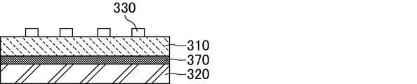
- the wiring pattern 30 is formed on the first resin 10.
- the method of forming the wiring pattern 30 is not particularly limited.
- the first resin 10 may be covered with a metal film, and the wiring pattern 30 may be formed by etching the metal film.
- the wiring pattern 30 may be formed by printing a conductive paste.
- the first resin 10 is covered with a metal film.
- the method of covering the first resin 10 with a metal film is not particularly limited, and a method of attaching a metal foil or a method of forming a metal film on the first resin 10 by plating may be mentioned.
- metal which comprises a metal film For example, copper, silver, etc. are mentioned. Among these, copper is desirable.
- the metal film covering the first resin 10 is masked and etched so as to form a predetermined wiring pattern.
- the etching can be performed by a conventional method in accordance with the type of metal constituting the metal film and the thickness of the metal film.
- the metal forming the metal film is copper, it is desirable to perform etching using a sulfuric acid / hydrogen peroxide type etching solution or the like as the etching solution.
- the conductive paste is not particularly limited, but, for example, a blend of a conductive filler, a thermosetting resin, and a thermoplastic resin can be used.
- a conductive filler metal particles, carbon nanotubes, carbon fibers, metal fibers and the like can be used.
- the first resin 10 is irradiated with light 50 to cure the first resin 10, thereby fixing the wiring pattern 30 to the first resin 10. Do. Since the first resin 10 contains the first polymerization initiator which is a photopolymerization initiator, the first resin 10 is cured by being irradiated with the light 50.
- the conditions such as the wavelength of the light 50 and the irradiation time are not particularly limited as long as the first resin 10 can be cured while maintaining the semi-cured state of the second resin 20, the type of the first resin 10 and It is desirable to set appropriately according to the type of first polymerization initiator.
- a polyimide resin is used as the first resin 10
- 1,2-octanedione, 1- [4- (phenylthio) -2- (O-benzoyloxime)] manufactured by BASF Japan Ltd.
- IRGACURE OXE-01 Ethanone, 1- [9-ethyl-6- (2-methylbenzoyl) -9H-carbazol-3-yl] -1- (O-acetyloxime) (manufactured by BASF Japan Ltd.),
- a photopolymerization initiator such as IRGACURE OXE-02 "
- 2,4-dimethylthioxanthone having a thioxanthone structure Nippon Kayaku Co., Ltd.
- DETX-S the light 50 has a wavelength of 310 to 436 nm Is desirable.
- the wiring pattern 30 formed on the first resin 10 is fixed, so the adhesion between the wiring pattern 30 and the first resin 10 can be improved.
- the base 40 may have not only a function as a heat dissipating material but also a function as a reinforcing material.
- the base 40 is not particularly limited, and may be made of aluminum, iron, SUS, copper, tin, ceramics, glass, a carbon-based compound such as graphene, or the like.
- a reflective material or the like may be applied to the surface of the base 40 opposite to the side to be bonded to the second resin 20.
- the substrate 40 when the substrate 40 is made of aluminum, the substrate 40 functions as a heat dissipating material as well as a reinforcing material.
- the thickness of the substrate 40 is desirably 5 to 100 ⁇ m, and more desirably 10 to 50 ⁇ m.
- Second Resin Curing Step As shown in FIG. 5, heat 60 is applied to the second resin 20. Since the second resin 20 contains the second polymerization initiator which is a thermal polymerization initiator, the heat 60 is applied to harden the second resin 20. By curing the second resin 20, the second resin 20 and the base 40 are bonded.
- the second resin 20 contains the second polymerization initiator which is a thermal polymerization initiator
- the conditions under which the heat 60 is applied are not particularly limited, and it is desirable to set appropriately according to the type of the second resin 20 and the type of the second polymerization initiator.
- the temperature of the heat 60 is 50 to 200 ° C. It is desirable to have.
- a printed wiring board can be manufactured through the above steps.
- the first polymerization initiator is a photopolymerization initiator and a thermal polymerization initiator
- the second polymerization initiator is a thermal polymerization initiator. It may be In this case, (3) in the first resin curing step, the first resin 10 is cured by irradiating the first resin 10 with light, and (5) in the second resin curing step, the second Heat is applied to the resin 20 to cure the second resin 20, and at the same time, heat is applied to the first resin 10 to cure the first resin 10.
- the degree of curing of the first resin 10 can be easily controlled in the first resin curing step.
- heat is also applied to the first resin 10 to cure the second resin 20 and at the same time, if an uncured portion exists in the first resin 10, the first resin Ten uncured portions can be sufficiently cured.
- the first resin 10 may be cured so that the first resin 10 is not completely cured.
- the desired type of the thermal polymerization initiator contained in the first polymerization initiator is the same as the desired type of the thermal polymerization initiator contained in the second polymerization initiator.
- the wiring pattern is embedded in the first resin as needed. May be.
- the position of the wiring pattern can be easily fixed, so that the wiring pattern can be prevented from being displaced.
- the wiring pattern may be embedded so that the wiring pattern and the first resin are substantially flush, or only a part of the wiring pattern may be embedded in the first resin.
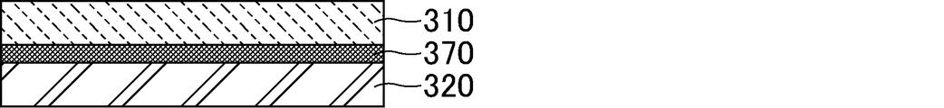
- the first resin and / or the second resin is impregnated between the first resin and the second resin. It is desirable to place possible reinforcements.
- the reinforcing material By arranging the reinforcing material between the first resin and the second resin, the strength of the printed wiring board to be manufactured can be strengthened.
- the reinforcing material can be impregnated with the first resin and / or the second resin, the first resin and the second resin are in direct contact with each other. Therefore, the adhesion between the first resin and the second resin is not easily inhibited.
- a reinforcing material in which the second resin can be impregnated is disposed between the second resin and the base material. It is desirable to do. By arranging the reinforcing material between the second resin and the base material, the strength of the printed wiring board to be manufactured can be strengthened. In addition, since the reinforcing material can be impregnated with the second resin, the second resin and the base material are in direct contact with each other. Therefore, the adhesion between the second resin and the base is unlikely to be inhibited.
- the reinforcing material is not particularly limited, but may be, for example, a porous body of a fluorine-based resin sheet such as PTFE, or a fibrous body such as glass cloth, cellulose fiber cloth, or paper.
- the method for producing a printed wiring board according to the second embodiment of the present invention includes (1) resin laminating step to (5) second resin curing step, and the first polymerization initiator is a thermal polymerization initiator.
- the second polymerization initiator is a photopolymerization initiator.
- (3) in the first resin curing step the first resin is cured by applying heat to the first resin, and (5) in the second resin curing step, the second resin is irradiated with light. The second resin is cured.
- FIG. 6 is a schematic diagram which shows typically an example of the lamination process in the manufacturing method of the printed wiring board which concerns on 2nd Embodiment of this invention.
- FIG. 7 is a schematic diagram which shows typically an example of the wiring pattern formation process in the manufacturing method of the printed wiring board which concerns on 2nd Embodiment of this invention.
- FIG. 8 is a schematic diagram which shows typically an example of the 1st resin hardening process in the manufacturing method of the printed wiring board which concerns on 2nd Embodiment of this invention.
- FIG. 6 is a schematic diagram which shows typically an example of the lamination process in the manufacturing method of the printed wiring board which concerns on 2nd Embodiment of this invention.
- FIG. 7 is a schematic diagram which shows typically an example of the wiring pattern formation process in the manufacturing method of the printed wiring board which concerns on 2nd Embodiment of this invention.
- FIG. 8 is a schematic diagram which shows typically an example of the 1st resin hardening process in the manufacturing method of the printed wiring board which concerns on 2nd
- FIG. 9 is a schematic diagram which shows typically an example of the base-material bonding process in the manufacturing method of the printed wiring board which concerns on 2nd Embodiment of this invention.
- FIG. 10 is a schematic view schematically showing an example of a second resin curing step in the method for manufacturing a printed wiring board according to the second embodiment of the present invention.
- the desirable material, thickness, relative dielectric constant, dielectric tangent and the like of the first resin 110 are the desirable materials of the first resin 10 described in the description of the method for producing a printed wiring board according to the first embodiment of the present invention, Same as thickness, dielectric constant, and dielectric loss tangent.
- the first resin 110 contains a first polymerization initiator which is a thermal polymerization initiator.
- the first polymerization initiator is not particularly limited as long as it is a thermal polymerization initiator, and may be, for example, an organic peroxide thermal polymerization initiator, an azo thermal polymerization initiator, or the like.
- the desirable material and thickness of the second resin 120 are the same as the desirable material and thickness of the second resin 20 described in the method of manufacturing a printed wiring board according to the first embodiment of the present invention. Also, the second resin 120 may contain a functional material, as in the case of the second resin 20.
- the second resin 120 contains a second polymerization initiator which is a photopolymerization initiator.
- the second polymerization initiator is not particularly limited as long as it is a photopolymerization initiator, and may be, for example, an alkylphenone type, an acyl phosphine type, an oxime ester type, a thioxanthone type, and the like.
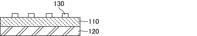
- the wiring pattern 130 is formed on the first resin 110.
- the method and material for forming the wiring pattern 130 are the same as the method and material for forming the wiring pattern 30 described in the method for manufacturing a printed wiring board according to the first embodiment of the present invention.
- heat 160 is applied to the first resin 110. Since the first resin 110 contains the first polymerization initiator which is a thermal polymerization initiator, the heat 160 is applied to harden the first resin 110.
- the conditions for applying the heat 160 are not particularly limited as long as the first resin 110 can be cured while maintaining the semi-cured state of the second resin 120, and the type of the first resin 110 and the first polymerization initiator are not particularly limited. It is desirable to set appropriately according to the type. For example, when a polyimide resin is used as the first resin 110 and t-butylperoxypivalate is used as the first polymerization initiator, the temperature of the heat 160 is desirably 60 to 90 ° C.
- the wiring pattern 130 formed in the first resin 110 is fixed, so that the adhesion between the wiring pattern 130 and the first resin 110 can be improved.
- the desired material and the like of the substrate 140 may be the same as the desired material and the like of the substrate 40 described in the description of the method for manufacturing a printed wiring board according to the first embodiment of the present invention.
- the base material 140 may have translucency.
- the substrate 140 has translucency
- light from the substrate 140 side can also reach the second resin 120 in the (5) second resin curing step described later. Therefore, the second resin 120 can be cured efficiently.
- examples of the material of the base material 140 include translucent inorganic materials such as glass and quartz, and translucent organic materials such as acrylic resin, polycarbonate resin and cycloolefin resin.
- translucent means that the base material transmits light so that the curing of the second resin proceeds when irradiated with light for curing the second resin from the base material side.
- the second resin 120 is irradiated with light 150. Since the second resin 120 contains a second polymerization initiator which is a photopolymerization initiator, the second resin 120 is cured by being irradiated with the light 150. By curing the second resin 120, the second resin 120 and the base 140 are bonded.
- a second polymerization initiator which is a photopolymerization initiator
- the conditions for irradiating the light 150 are not particularly limited, and it is desirable to appropriately set the conditions according to the type of the second resin 120 and the type of the second polymerization initiator.
- a polyimide resin is used as the second resin 120, and 1,2-octanedione, 1- [4- (phenylthio) -2- (O-benzoyloxime)] (manufactured by BASF Japan Ltd.) as the second polymerization initiator.
- UVGACURE OXE-01 Ethanone, 1- [9-ethyl-6- (2-methylbenzoyl) -9H-carbazol-3-yl] -1- (O-acetyloxime) (manufactured by BASF Japan Ltd.),
- a photopolymerization initiator such as IRGACURE OXE-02 "
- 2,4-dimethylthioxanthone having a thioxanthone structure Nippon Kayaku Co., Ltd.
- DETX-S the wavelength of light 150 is 310 to 436 nm Is desirable.
- the base material 140 has translucency
- the substrate 140 has translucency
- the light 150 irradiated from the substrate 140 side can also reach the second resin 120. Therefore, the second resin 120 can be cured efficiently.
- a printed wiring board can be manufactured through the above steps.
- the first polymerization initiator is a thermal polymerization initiator and a photopolymerization initiator
- the second polymerization initiator is a photopolymerization initiator It may be In this case, (3) in the first resin curing step, the first resin 110 is cured by applying heat to the first resin 110, and (5) in the second resin curing step, the second resin is cured. The second resin 120 is cured by irradiating 120 with light, and at the same time, the first resin 110 is cured by irradiating the first resin 110 with light.
- the first resin 110 includes the first polymerization initiator including the thermal polymerization initiator and the photopolymerization initiator, it is easy to control the degree of curing of the first resin 110 in the first resin curing step. Become. In the second resin curing step, the first resin 110 is also irradiated with light to cure the second resin 120 and at the same time, if there is an uncured portion in the first resin 110, the first resin 110 is cured. The uncured portion of the resin 110 can be sufficiently cured. In the (3) first resin curing step, the first resin 110 may be cured so that the first resin 110 is not completely cured.
- (1) after forming the wiring pattern in the first resin in the wiring pattern forming step, embedding the wiring pattern in the first resin as necessary May be.
- the position of the wiring pattern can be easily fixed, so that the wiring pattern can be prevented from being displaced.
- the wiring pattern may be embedded so that the wiring pattern and the first resin are substantially flush, or only a part of the wiring pattern may be embedded in the first resin.
- the first resin and / or the second resin is impregnated between the first resin and the second resin. It is desirable to place possible reinforcements.
- the reinforcing material By arranging the reinforcing material between the first resin and the second resin, the strength of the printed wiring board to be manufactured can be strengthened.
- the reinforcing material can be impregnated with the first resin and / or the second resin, the first resin and the second resin are in direct contact with each other. Therefore, the adhesion between the first resin and the second resin is not easily inhibited.
- a reinforcing material in which the second resin can be impregnated is disposed between the second resin and the base material. It is desirable to do. By arranging the reinforcing material between the second resin and the base material, the strength of the printed wiring board to be manufactured can be strengthened. In addition, since the reinforcing material can be impregnated with the second resin, the second resin and the base material are in direct contact with each other. Therefore, the adhesion between the second resin and the base is unlikely to be inhibited.
- the reinforcing material is not particularly limited, but is preferably made of a material having a low dielectric constant and a dielectric loss tangent. If the reinforcing material is made of a material having a low dielectric constant and a dielectric loss tangent, the transmission characteristics of the printed wiring board to be produced will be good.
- a reinforcing material may be, for example, a porous body of a fluorine-based resin sheet such as PTFE, or may be a fibrous body such as glass cloth, cellulose fiber cloth, or paper.
- the method for producing a printed wiring board according to the third embodiment of the present invention includes (1) resin laminating step to (5) second resin curing step, and the first polymerization initiator is a thermal polymerization initiator.
- the second polymerization initiator is a thermal polymerization initiator.
- the first resin curing step heat is applied at a temperature at which the second resin remains in a semi-cured state and at which the first resin cures, and the first resin is cured.
- the resin may be cured, and in the second resin curing step, heat at a temperature at which the second resin cures may be added to cure the second resin. That is, by adjusting the composition of the first resin and the second resin so that the curing temperature of the first resin is lower than the curing temperature of the second resin, the curing time of the first resin and the curing of the second resin You may stagger the time.
- the first resin can be cured without completely curing the second resin.
- the position of the wiring pattern formed in the first resin can be easily fixed, so that the wiring pattern can be prevented from being displaced.
- the adhesion to the substrate is improved.
- the method of setting the curing temperature of the first resin lower than the curing temperature of the second resin is not particularly limited, and may be adjusted by selecting the type of resin and the type of thermal polymerization initiator, and additives may be added. May be adjusted.
- the 10 hour half-life temperature of the first polymerization initiator is higher than the 10 hour half-life temperature of the second polymerization initiator There is a way to lower it.
- the first resin is cured by applying heat to the first resin at a temperature lower than the 10 hour half-life temperature of the second polymerization initiator
- the second resin may be cured by applying heat to the second resin at a temperature higher than the 10-hour half-life temperature of the second polymerization initiator.
- the second heat treatment can be easily performed by controlling the temperature of heat in the first resin curing step and the second resin curing step.
- the curing of the first resin can be performed prior to the curing of the resin.
- FIG. 11 is a schematic diagram which shows typically an example of the lamination process in the manufacturing method of the printed wiring board which concerns on 3rd Embodiment of this invention.
- FIG. 12 is a schematic diagram which shows typically an example of the wiring pattern formation process in the manufacturing method of the printed wiring board which concerns on 3rd Embodiment of this invention.
- FIG. 13 is a schematic diagram which shows typically an example of the 1st resin hardening process in the manufacturing method of the printed wiring board which concerns on 3rd Embodiment of this invention.
- FIG. 11 is a schematic diagram which shows typically an example of the lamination process in the manufacturing method of the printed wiring board which concerns on 3rd Embodiment of this invention.
- FIG. 12 is a schematic diagram which shows typically an example of the wiring pattern formation process in the manufacturing method of the printed wiring board which concerns on 3rd Embodiment of this invention.
- FIG. 13 is a schematic diagram which shows typically an example of the 1st resin hardening process in the manufacturing method of the printed wiring board
- FIG. 14 is a schematic diagram which shows typically an example of the base-material bonding process in the manufacturing method of the printed wiring board which concerns on 3rd Embodiment of this invention.
- FIG. 15 is a schematic diagram which shows typically an example of the 2nd resin hardening process in the manufacturing method of the printed wiring board which concerns on 3rd Embodiment of this invention.
- the desirable material, thickness, relative dielectric constant, dielectric tangent and the like of the first resin 210 are the desirable materials of the first resin 10 described in the description of the method for producing a printed wiring board according to the first embodiment of the present invention, Same as thickness, dielectric constant, and dielectric loss tangent.
- the desirable material and thickness of the second resin 220 are the same as the desirable material and thickness of the second resin 20 described in the method of manufacturing a printed wiring board according to the first embodiment of the present invention. Also, the second resin 220 may contain a functional material, as in the case of the second resin 20.
- the first resin 210 and the second resin 220 each contain a first polymerization initiator which is a thermal polymerization initiator and a second polymerization initiator which is a thermal polymerization initiator.
- the 10-hour half-life temperature of the first polymerization initiator is desirably lower than the 10-hour half-life temperature of the second polymerization initiator.
- the 10-hour half-life temperature of the first polymerization initiator is preferably 30 to 150 ° C., and more preferably 50 to 90 ° C.
- the first polymerization initiator is not particularly limited.
- t-butylperoxypivalate t-hexylperoxypivalate, 1,1,3,3-tetramethylbutylperoxy-2-ethylhexano It may be ethe.
- the second polymerization initiator is not particularly limited, and may be, for example, t-hexylperoxyisopropyl monocarbonate, t-butylperoxy laurate or the like.
- the wiring pattern 230 is formed on the first resin 210.
- the method and material for forming the wiring pattern 230 are the same as the method and material for forming the wiring pattern 30 described in the method for manufacturing a printed wiring board according to the first embodiment of the present invention.
- the conditions for applying the heat 261 are not particularly limited as long as the temperature of the heat 261 is a temperature at which the second resin remains in a semi-cured state and the temperature at which the first resin cures. It is desirable to set appropriately according to the type of the resin 210 and the first polymerization initiator.
- the temperature of heat 261 is preferably 10 to 100 ° C. lower than the 10-hour half-life temperature of the second polymerization initiator, and more preferably 10 to 80 ° C. lower.
- the temperature of the heat 261 is desirably 60 to 90 ° C.
- the wiring pattern 230 embedded in the first resin 210 is fixed, so that the adhesion between the wiring pattern 230 and the first resin 210 can be improved.
- the desirable material and the like of the substrate 240 may be the same as the desirable material and the like of the substrate 40 described in the description of the method of manufacturing a printed wiring board according to the first embodiment of the present invention.
- the conditions to which the heat 262 is applied are not particularly limited as long as the temperature of the heat 262 is a temperature at which the second resin cures, and it is desirable to appropriately set according to the types of the second resin 220 and the second polymerization initiator .
- the temperature of heat 262 is preferably 10 to 100 ° C. higher than the 10-hour half-life temperature of the second polymerization initiator, and more preferably 10 to 50 ° C. higher.
- the temperature of the heat 262 is desirably 120 to 200 ° C.
- a printed wiring board can be manufactured through the above steps.
- the wiring pattern is embedded in the first resin as needed. May be.
- the position of the wiring pattern can be easily fixed, so that the wiring pattern can be prevented from being displaced.
- the wiring pattern may be embedded so that the wiring pattern and the first resin are substantially flush, or only a part of the wiring pattern may be embedded in the first resin.
- the first resin and / or the second resin is impregnated between the first resin and the second resin. It is desirable to place possible reinforcements.
- the reinforcing material By arranging the reinforcing material between the first resin and the second resin, the strength of the printed wiring board to be manufactured can be strengthened.
- the reinforcing material can be impregnated with the first resin and / or the second resin, the first resin and the second resin are in direct contact with each other. Therefore, the adhesion between the first resin and the second resin is not easily inhibited.
- a reinforcing material in which the second resin can be impregnated is arranged between the second resin and the base material. It is desirable to do. By arranging the reinforcing material between the second resin and the base material, the strength of the printed wiring board to be manufactured can be strengthened. In addition, since the reinforcing material can be impregnated with the second resin, the second resin and the base material are in direct contact with each other. Therefore, the adhesion between the second resin and the base is unlikely to be inhibited.
- the reinforcing material is not particularly limited, but may be, for example, a porous body of a fluorine-based resin sheet such as PTFE, or a fibrous body such as glass cloth, cellulose fiber cloth, or paper.
- the method for producing a printed wiring board according to the fourth embodiment of the present invention includes (1) resin laminating step to (5) second resin curing step, and the first polymerization initiator is a photopolymerization initiator.
- the second polymerization initiator is a photopolymerization initiator.
- the base material has translucency.
- the first resin and the second resin are laminated with the light impermeable layer interposed between the first resin and the second resin.
- the first resin is cured by irradiating the first resin with light from the first resin side
- the second resin curing step from the base material side
- the second resin is cured by irradiating the second resin with light.
- FIG. 16 is a schematic diagram which shows typically an example of the lamination process in the manufacturing method of the printed wiring board which concerns on 4th Embodiment of this invention.
- FIG. 17 is a schematic diagram which shows typically an example of the wiring pattern formation process in the manufacturing method of the printed wiring board which concerns on 4th Embodiment of this invention.
- FIG. 18 is a schematic view schematically showing an example of a first resin curing step in the method for manufacturing a printed wiring board according to the fourth embodiment of the present invention.
- FIG. 19 is a schematic diagram which shows typically an example of the base-material bonding process in the manufacturing method of the printed wiring board which concerns on 4th Embodiment of this invention.
- FIG. 20 is a schematic view schematically showing an example of a second resin curing step in the method for manufacturing a printed wiring board according to the fourth embodiment of the present invention.
- the desirable material, thickness, relative dielectric constant, dielectric tangent and the like of the first resin 310 are the desirable materials of the first resin 10 described in the description of the method for producing a printed wiring board according to the first embodiment of the present invention, Same as thickness, dielectric constant, and dielectric loss tangent.
- the first resin 310 contains a first polymerization initiator which is a photopolymerization initiator.
- the first polymerization initiator is not particularly limited as long as it is a photopolymerization initiator, and for example, an alkylphenone photopolymerization initiator, an acylphosphine photopolymerization initiator, an oxime ester photopolymerization initiator, a thioxanthone type Photopolymerization initiators can be mentioned.
- the desirable material and thickness of the second resin 320 are the same as the desirable material and thickness of the second resin 20 described in the method of manufacturing a printed wiring board according to the first embodiment of the present invention.
- the second resin 320 may contain a functional material, as in the case of the second resin 20.
- the second resin 320 contains a second polymerization initiator which is a photopolymerization initiator.
- the second polymerization initiator is not particularly limited as long as it is a photopolymerization initiator, and, for example, an alkylphenone photopolymerization initiator, an acylphosphine photopolymerization initiator, an oxime ester photopolymerization initiator, Thioxanthone photopolymerization initiators can be mentioned.
- the material of the light impermeable layer 370 is not particularly limited, and examples thereof include metals such as copper and aluminum, resin films containing a pigment, and ceramic sheets.
- the thickness of the light impermeable layer 370 is not particularly limited, but is preferably 0.1 to 500 ⁇ m, and more preferably 0.5 to 300 ⁇ m.
- the wiring pattern 330 is formed on the first resin 310.
- the method and material for forming the wiring pattern 330 are the same as the method and material for forming the wiring pattern 30 described in the method for manufacturing a printed wiring board according to the first embodiment of the present invention.
- the first resin 310 is irradiated with the light 351 from the first resin 310 side. Since the first resin 310 contains the first polymerization initiator which is a photopolymerization initiator, the first resin 310 is cured by being irradiated with the light 351. In addition, since the light 351 is blocked by the light impermeable layer 370 and does not reach the second resin 320, the semi-cured state of the second resin is maintained.
- the first polymerization initiator which is a photopolymerization initiator
- the conditions such as the wavelength of the light 351 and the irradiation time are not particularly limited, and it is desirable to set appropriately according to the type of the first resin 310 and the type of the first polymerization initiator.
- a polyimide resin is used as the first resin 310, and 1,2-octanedione, 1- [4- (phenylthio) -2- (O-benzoyloxime)] (BASF Japan Ltd.) is used as the first polymerization initiator.
- UVGACURE OXE-01 Ethanone, 1- [9-ethyl-6- (2-methylbenzoyl) -9H-carbazol-3-yl] -1- (O-acetyloxime) (manufactured by BASF Japan Ltd.),
- a photopolymerization initiator such as IRGACURE OXE-02 "
- 2,4-dimethylthioxanthone having a thioxanthone structure Nippon Kayaku Co., Ltd.
- DETX-S the wavelength of light 351 is 310 to 436 nm Is desirable.
- the wiring pattern 330 embedded in the first resin 310 is fixed, so that the adhesion between the wiring pattern 330 and the first resin 310 can be improved.
- the base material 340 may be made of any material as long as it has a light transmitting property, for example, a light transmitting inorganic material such as glass or quartz, or a light transmitting such as an acrylic resin, a polycarbonate resin, or a cycloolefin resin It may be made of organic material or the like.
- the second resin 320 is irradiated with light 352 from the base material 340 side. Since the substrate 340 has translucency, the light 352 passes through the substrate 340 and reaches the second resin 320. Further, since the second resin 320 contains the second polymerization initiator which is a photopolymerization initiator, the second resin 320 is cured by the light 352. Then, the second resin 320 and the base 340 are bonded by curing of the second resin 320.
- the conditions for irradiating the light 352 are not particularly limited, and it is desirable to appropriately set the conditions according to the type of the second resin 320 and the type of the second polymerization initiator.
- a polyimide resin is used as the second resin 320, and 1,2-octanedione, 1- [4- (phenylthio) -2- (O-benzoyloxime)] (manufactured by BASF Japan Ltd.) as the second polymerization initiator.
- UVGACURE OXE-01 Ethanone, 1- [9-ethyl-6- (2-methylbenzoyl) -9H-carbazol-3-yl] -1- (O-acetyloxime) (manufactured by BASF Japan Ltd.),
- a photopolymerization initiator such as IRGACURE OXE-02
- 2,4-dimethylthioxanthone having a thioxanthone structure Nippon Kayaku Co., Ltd.
- DETX-S the wavelength of light 352 is 310 to 436 nm Is desirable.
- a printed wiring board can be manufactured through the above steps.
- (1) after forming the wiring pattern in the first resin in the wiring pattern forming step, embedding the wiring pattern in the first resin as necessary May be.
- the position of the wiring pattern can be easily fixed, so that the wiring pattern can be prevented from being displaced.
- the wiring pattern may be embedded so that the wiring pattern and the first resin are substantially flush, or only a part of the wiring pattern may be embedded in the first resin.
- a reinforcing material in which the second resin can be impregnated is disposed between the second resin and the base material. It is desirable to do. By arranging the reinforcing material between the second resin and the base material, the strength of the printed wiring board to be manufactured can be strengthened. In addition, since the reinforcing material can be impregnated with the second resin, the second resin and the base material are in direct contact with each other. Therefore, the adhesion between the second resin and the base is unlikely to be inhibited.
- the reinforcing material is not particularly limited, but may be, for example, a porous body of a fluorine-based resin sheet such as PTFE, or a fibrous body such as glass cloth, cellulose fiber cloth, or paper.
- the method of manufacturing a printed wiring board according to the fifth embodiment of the present invention includes (1) resin laminating step to (5) second resin curing step.
- the first polymerization initiator functions as a photopolymerization initiator by being irradiated with light of a first wavelength
- the second polymerization initiator is a photopolymerization initiator by being irradiated with light of a second wavelength Act as.
- the first wavelength and the second wavelength are different wavelengths.
- the first resin is irradiated with light of the first wavelength while the semi-cured state of the second resin is maintained, and the first resin is cured;
- the second resin curing step the second resin is cured by irradiating the second resin with light of the second wavelength.
- FIG. 21 is a schematic diagram which shows typically an example of the lamination process in the manufacturing method of the printed wiring board which concerns on 5th Embodiment of this invention.
- FIG. 22 is a schematic diagram which shows typically an example of the wiring pattern formation process in the manufacturing method of the printed wiring board which concerns on 5th Embodiment of this invention.
- FIG. 23 is a schematic diagram which shows typically an example of the 1st resin hardening process in the manufacturing method of the printed wiring board which concerns on 5th Embodiment of this invention.
- FIG. 21 is a schematic diagram which shows typically an example of the lamination process in the manufacturing method of the printed wiring board which concerns on 5th Embodiment of this invention.
- FIG. 22 is a schematic diagram which shows typically an example of the wiring pattern formation process in the manufacturing method of the printed wiring board which concerns on 5th Embodiment of this invention.
- FIG. 23 is a schematic diagram which shows typically an example of the 1st resin hardening process in the manufacturing method of the printed wiring board which concerns on 5th
- FIG. 24 is a schematic diagram which shows typically an example of the base-material bonding process in the manufacturing method of the printed wiring board which concerns on 5th Embodiment of this invention.
- FIG. 25 is a schematic diagram which shows typically an example of the 2nd resin hardening process in the manufacturing method of the printed wiring board which concerns on 5th Embodiment of this invention.
- the desirable material, thickness, relative dielectric constant, dielectric tangent and the like of the first resin 410 are the desirable materials of the first resin 10 described in the description of the method for producing a printed wiring board according to the first embodiment of the present invention, Same as thickness, dielectric constant, and dielectric loss tangent.
- the desirable material and thickness of the second resin 420 are the same as the desirable material and thickness of the second resin 20 described in the method of manufacturing a printed wiring board according to the first embodiment of the present invention. Further, the second resin 420 may contain a functional material, as in the case of the second resin 20.
- the first resin 410 and the second resin 420 are each irradiated with light of a first wavelength, and are thus irradiated with light of a first polymerization initiator that functions as a photopolymerization initiator and light of a second wavelength. It contains a second polymerization initiator that functions as an initiator. Also, the first wavelength and the second wavelength are different wavelengths. The first wavelength and the second wavelength preferably differ by 50 nm or more, and more preferably by 100 nm or more.
- the first resin containing the first polymerization initiator by irradiating the light of the first wavelength in the (4) first resin curing step described later to be a wavelength that the first wavelength and the second wavelength differ by 50 nm or more Even when light of the first wavelength reaches the second resin containing the second polymerization initiator when curing the second resin, the second resin can easily maintain the semi-cured state.
- the wiring pattern 430 is formed on the first resin 410.
- the method and material for forming the wiring pattern 430 are the same as the method and material for forming the wiring pattern 30 described in the method for manufacturing a printed wiring board according to the first embodiment of the present invention.
- Conditions such as the first wavelength at the time of irradiation with the light 451 and the irradiation time are not particularly limited, and it is desirable to set appropriately according to the type of the first resin 410 and the type of the first polymerization initiator.
- a polyimide resin is used as the first resin 410, and 1,2-octanedione, 1- [4- (phenylthio) -2- (O-benzoyloxime)] (manufactured by BASF Japan Ltd.) as the first polymerization initiator.
- IRGACURE OXE-01 Ethanone, 1- [9-ethyl-6- (2-methylbenzoyl) -9H-carbazol-3-yl] -1- (O-acetyloxime) (manufactured by BASF Japan Ltd.),
- a photopolymerization initiator such as IRGACURE OXE-02 "
- 2,4-dimethylthioxanthone having a thioxanthone structure DETX-S "manufactured by Nippon Kayaku Co., Ltd.
- the first wavelength of the light 451 is 200 It is desirable that the thickness be about 400 nm.
- the desirable material and the like of the substrate 440 may be the same as the desirable material and the like of the substrate 40 described in the description of the method for manufacturing a printed wiring board according to the first embodiment of the present invention.
- the base 440 may have a light transmitting property.
- the base 440 has translucency, light of the second wavelength can also reach the second resin 420 from the base 440 side in the (5) second resin curing step described later. Therefore, the second resin 420 can be efficiently cured.
- the substrate 440 has translucency, examples of the material of the substrate 440 include translucent inorganic materials such as glass and quartz, and translucent organic materials such as acrylic resin, polycarbonate resin and cycloolefin resin.
- the second resin 420 is irradiated with the light 452 of the second wavelength to cause the second polymerization initiator to function as a photopolymerization initiator, the second The resin 420 is cured. By curing the second resin 420, the second resin 420 and the base 440 are bonded.
- Conditions such as the second wavelength at the time of irradiation of the light 452 and the irradiation time are not particularly limited, and it is desirable to set appropriately according to the type of the second resin 420 and the type of the second polymerization initiator.
- the first wavelength of the light 452 be 480 to 600 nm.
- the base material 440 has translucency
- the substrate 440 has translucency
- the light 452 of the second wavelength emitted from the substrate 440 side can also reach the second resin 420. Therefore, the second resin 420 can be efficiently cured.
- a printed wiring board can be manufactured through the above steps.
- (1) after forming the wiring pattern in the first resin in the wiring pattern forming step, embedding the wiring pattern in the first resin as necessary May be.
- the position of the wiring pattern can be easily fixed, so that the wiring pattern can be prevented from being displaced.
- the wiring pattern may be embedded so that the wiring pattern and the first resin are substantially flush, or only a part of the wiring pattern may be embedded in the first resin.
- the first resin and / or the second resin is impregnated between the first resin and the second resin. It is desirable to place possible reinforcements.
- the reinforcing material By arranging the reinforcing material between the first resin and the second resin, the strength of the printed wiring board to be manufactured can be strengthened.
- the reinforcing material can be impregnated with the first resin and / or the second resin, the first resin and the second resin are in direct contact with each other. Therefore, the adhesion between the first resin and the second resin is not easily inhibited.
- a reinforcing material in which the second resin can be impregnated is disposed between the second resin and the base material. It is desirable to do. By arranging the reinforcing material between the second resin and the base material, the strength of the printed wiring board to be manufactured can be strengthened. In addition, since the reinforcing material can be impregnated with the second resin, the second resin and the base material are in direct contact with each other. Therefore, the adhesion between the second resin and the base is unlikely to be inhibited.
- the reinforcing material is not particularly limited, but may be, for example, a porous body of a fluorine-based resin sheet such as PTFE, or a fibrous body such as glass cloth, cellulose fiber cloth, or paper.
- 26 (a) to 26 (e) are schematic views schematically showing an example of a method of manufacturing a printed wiring board according to a sixth embodiment of the present invention in the order of steps.
- the first resin 510 in a semi-cured state and the second resin 520 in a semi-cured state are laminated by a first roll press 581. That is, (1) a resin laminating step is performed.
- the first resin 510 contains a first polymerization initiator
- the second resin 520 contains a second polymerization initiator.
- the materials of the first resin 510, the second resin 520, the first polymerization initiator, and the second polymerization initiator are the first resin and the second resin described in the first to fifth embodiments of the present invention. Materials of resin, first polymerization initiator, and second polymerization initiator can be used.
- the wiring pattern 530 is formed on the first resin 510. That is, (2) a wiring pattern formation step is performed.
- the method of forming the wiring pattern 530 on the first resin 510 is not particularly limited.
- a copper foil is attached to the first resin 510, the copper foil is masked with an etching resist, and the copper foil is etched using an etching solution.
- a wiring pattern having an arbitrary shape may be formed, and the wiring pattern 530 may be formed by removing the etching solution and the etching resist.
- a method of printing the wiring pattern 530 on the first resin 510 by a wiring pattern printing machine can also be mentioned. At this time, the wiring pattern 530 may be embedded in the first resin 510.
- the first resin 510 is cured by the first curing means 555. That is, (3) a first resin curing step is performed.
- the first curing means 555 for curing the first resin 510 it is desirable to appropriately select according to the type of the first resin 510 and the type of the first polymerization initiator.
- Examples of the first curing means 555 include light and heat, as described in the first to fifth embodiments of the present invention.
- the laminated first resin 510 and second resin 520 may be placed in a heating furnace and heated.
- the base material 540 is attached to the second resin 520. That is, (4) base material bonding process is performed.
- the material of the substrate 540 the materials of the substrates described in the first to fifth embodiments of the present invention can be used.
- the second resin 520 is cured by the second curing means 556. That is, (5) A second resin curing step is performed. Thereby, the second resin 520 and the base material 540 can be adhered, and a printed wiring board can be manufactured.
- the second curing unit 556 for curing the second resin 520 is desirably selected appropriately in accordance with the type of the second resin 520 and the type of the second polymerization initiator.
- Examples of the second curing means 556 include light and heat as described in the first to fifth embodiments of the present invention.
- the printed wiring board may be manufactured by continuously performing the above-described steps in a roll press.
- a thermal polymerization initiator is used as the first polymerization initiator and the second polymerization initiator, and the first curing means 555 and the second curing means 556 are used.
- the printed wiring board may be manufactured as follows. In this case, the 10-hour half-life temperature of the first polymerization initiator is lower than the 10-hour half-life temperature of the second polymerization initiator.
- the steps up to (1) resin lamination step and (2) wiring pattern formation step are performed.
- the (3) first resin curing step heat is applied at a temperature at which the second resin 520 remains in a semi-cured state and at which the first resin 510 cures. , And the first resin 510 is cured. At this time, if the wiring pattern 530 can be in close contact with the first resin 510, the first resin 510 may not be completely cured.
- (4) base material pasting process is performed as mentioned above.
- the heat of the temperature at which the second resin 520 is cured is applied to cure the second resin 520.
- the substrate 540 is brought into close contact with the second resin 520.
- the second resin 520 may not be completely cured.
- the laminate of the wiring pattern 530, the first resin 510, the second resin 520, and the base material 540 is put in a heating furnace in a long state or a state of being wound in a roll shape.
- a third resin heating step of heating the first resin 510 and the second resin 520 so that the second resin 520 is completely cured is performed. By completely curing the first resin 510 and the second resin 520 finally in a heating furnace, a printed wiring board can be efficiently manufactured.
- first resin curing step it is desirable to cure the first resin 510 by applying heat to the first resin 510 at a temperature lower than the 10-hour half-life temperature of the second polymerization initiator.
- second resin curing step it is desirable to cure the second resin by applying heat to the second resin 520 at a temperature higher than the 10-hour half-life temperature of the second polymerization initiator.
- FIG. 27 is a schematic view schematically showing an example of the printed wiring board of the present invention.
- the printed wiring board 601 which is an example of the printed wiring board of the present invention, has a surface opposite to the surface 611 of the wiring pattern 630, the first cured resin layer 615, and the first cured resin layer 615.
- the printed wiring board is composed of the second cured resin layer 625 laminated on 612 and the base material 640 bonded to the surface 622 opposite to the surface 621 of the second cured resin layer 625 in contact with the first cured resin layer 615 is there.
- the first cured resin layer 615 is a cured resin in which the first resin is cured by the first polymerization initiator
- the second cured resin layer 625 is a cured resin in which the second resin is cured by the second polymerization initiator. is there.
- the first curing means for curing the first resin with the first polymerization initiator and the second means for curing the second resin with the second polymerization initiator are different.
- the materials of the first resin, the second resin, the first polymerization initiator, the second polymerization initiator, the wiring pattern 630, and the base material 640 are the same as those described in the first to sixth embodiments of the present invention. It is desirable that the material is a resin, a second resin, a first polymerization initiator, a second polymerization initiator, a wiring pattern, and a base material.
- the first curing means and the second curing means are means for curing the first resin and the second resin described in the first to sixth embodiments of the present invention.
- the printed wiring board 601 having such a configuration is a printed wiring board manufactured by the method for manufacturing a printed wiring board described in the first to sixth embodiments of the present invention. Therefore, in the printed wiring board 601, the adhesion between the second cured resin layer 625 and the base material 640 is sufficiently high. Furthermore, the wiring pattern 630 also has less deviation from the predetermined position.
- the printed wiring board 601 can also function as a flexible printed wiring board.
- the method for producing a multilayer printed wiring board according to the eighth embodiment of the present invention is a method for producing a multilayer printed wiring board, wherein an upper layer printed wiring board and a lower layer printed wiring board are laminated to produce a multilayer printed wiring board.
- Laminating a first resin in a semi-hardened state and a second resin in a semi-hardened state (1) forming an upper layer printed wiring board resin laminating step, and forming a first wiring pattern on the first resin (2) first A wiring pattern forming step, and curing the first resin while maintaining the semi-cured state of the second resin to produce an upper layer printed wiring board (3) a first resin curing step, and a second wiring for the third resin
- the lower layer printed wiring board on which the pattern is formed is prepared (4)
- the lower layer printed wiring board preparing step, and the lower layer printed wiring board is laminated under the upper layer printed wiring board (5) printed wiring board laminating step, Cure the resin, on top Adhering the printed circuit board and the lower printed wiring board (6) and a second resin curing step.
- the first resin contains a first polymerization initiator
- the second resin contains a second polymerization initiator.
- FIG. 28 is process drawing which shows typically an example of the resin lamination process for upper layer printed wiring boards in the manufacturing method of the multilayer printed wiring board which concerns on 8th Embodiment of this invention.
- FIG. 29 is a process chart schematically showing an example of a first wiring pattern forming step in the method for manufacturing a multilayer printed wiring board according to the eighth embodiment of the present invention.
- FIG. 30 is process drawing which shows typically an example of the 1st resin hardening process in the manufacturing method of the multilayer printed wiring board which concerns on 8th Embodiment of this invention.
- FIG. 28 is process drawing which shows typically an example of the resin lamination process for upper layer printed wiring boards in the manufacturing method of the multilayer printed wiring board which concerns on 8th Embodiment of this invention.
- FIG. 29 is a process chart schematically showing an example of a first wiring pattern forming step in the method for manufacturing a multilayer printed wiring board according to the eighth embodiment of the present invention.
- FIG. 30 is process drawing which shows typically an example of the 1st resin
- FIG. 31 is a process chart schematically showing an example of a lower layer printed wiring board preparing step in the method for manufacturing a multilayer printed wiring board according to the eighth embodiment of the present invention.
- FIG. 32 is process drawing which shows typically an example of the printed wiring board lamination
- FIG. 33 is process drawing which shows typically an example of the 2nd resin hardening process in the manufacturing method of the multilayer printed wiring board which concerns on 8th Embodiment of this invention.
- (1) Resin Laminating Process for Upper Layer Printed Wiring Board In the method for manufacturing a multilayer printed wiring board according to the eighth embodiment of the present invention, first, as shown in FIG. The second resin 1020 in the state is laminated. In a step after the method for manufacturing a multilayer printed wiring board of the present invention, a first wiring pattern is formed on the first resin, and the second resin and the lower layer printed wiring board are bonded. Manufactured by using a resin of a type that improves the transmission characteristics of the first wiring pattern as the first resin, and using a type of resin that improves the adhesion with the lower layer printed wiring board as the second resin In a multilayer printed wiring board, transmission characteristics and adhesion between the printed wiring boards can be compatible.
- the material of the first resin 1010 is not particularly limited, it is desirable that the material is a photocurable resin or a thermosetting resin.
- examples of such resin include phenol resin, polyester resin, polyimide resin, polysulfonic acid resin, polyetherimide resin, polyether ketone resin, polycarbonate resin, polyurethane resin, polysiloxane resin, polyamide resin and the like.
- polyimide resins are preferable.
- the polyimide resin is preferably a curable resin composition containing a (A) bismaleimide compound represented by the following general formula (1).
- X is an aliphatic, alicyclic or aromatic hydrocarbon group and is a hydrocarbon group having 10 to 30 carbon atoms in its main chain, and these groups are hetero compounds It may have an atom, a substituent or a siloxane skeleton.
- X is preferably an aliphatic or alicyclic hydrocarbon or an aliphatic hydrocarbon group modified by an alicyclic hydrocarbon group, and more preferably an aliphatic hydrocarbon group having 10 to 55 carbon atoms. And 10 to 40 carbon atoms are more preferable.
- Y represents an aliphatic, alicyclic or aromatic hydrocarbon group, and these groups have a hetero atom, a substituent, a phenyl ether skeleton, a sulfonyl skeleton or a siloxane skeleton It is also good.
- Y is preferably an aromatic hydrocarbon group.
- n is the number of repeating units and represents a number in the range of 1 to 20.
- a first wiring pattern is formed on the first resin 1010.
- the material of the first resin 1010 is the above-described resin, the transmission characteristics of the signal transmitted in the first wiring pattern are improved.
- the thickness of the first resin 1010 is not particularly limited, but is preferably 5 to 100 ⁇ m, and more preferably 10 to 100 ⁇ m. When the thickness of the first resin 10 is less than 5 ⁇ m, the strength of the upper layer printed wiring board tends to be weak. When the thickness of the first resin 1010 exceeds 100 ⁇ m, the multilayer printed wiring board to be manufactured becomes thick, and it becomes difficult to miniaturize the electronic device.
- the relative dielectric constant of the first resin 1010 is desirably 2 to 3 at a frequency of 1 GHz.
- the dielectric loss tangent of the first resin 1010 is preferably 0.0001 to 0.002 at a frequency of 1 GHz.
- the first resin 1010 contains a first polymerization initiator.
- the first polymerization initiator is a thermal polymerization initiator or a photopolymerization initiator.
- the type of the first polymerization initiator is the type of the second polymerization initiator, (3) the first curing means in the first resin curing step, and (6) the second curing means in the second resin curing step. It is desirable to select according to. These desirable examples will be described later.
- the material of the second resin 1020 is not particularly limited, for example, it is desirable to be a photocurable resin or a thermosetting resin.
- a photocurable resin or a thermosetting resin examples include phenol resin, polyester resin, polyimide resin, polysulfonic acid resin, polyetherimide resin, polyether ketone resin, polycarbonate resin, polyurethane resin, polysiloxane resin, polyamide resin and the like.
- polyimide resins are preferable.
- the polyimide resin is preferably a curable resin composition containing (A) a bismaleimide compound represented by the following general formula (1).
- X is an aliphatic, alicyclic or aromatic hydrocarbon group and is a hydrocarbon group having 10 to 30 carbon atoms in its main chain, and these groups are hetero compounds It may have an atom, a substituent or a siloxane skeleton.
- X is preferably an aliphatic or alicyclic hydrocarbon or an aliphatic hydrocarbon group modified by an alicyclic hydrocarbon group, and more preferably an aliphatic hydrocarbon group having 10 to 55 carbon atoms. And 10 to 40 carbon atoms are more preferable.
- Y represents an aliphatic, alicyclic or aromatic hydrocarbon group, and these groups have a hetero atom, a substituent, a phenyl ether skeleton, a sulfonyl skeleton or a siloxane skeleton It is also good.
- Y is preferably an aromatic hydrocarbon group.
- n is the number of repeating units and represents a number in the range of 1 to 20.
- the second resin 1020 is bonded to the third resin of the lower layer printed wiring board.
- the material of the second resin 1020 is the above-described resin, the adhesiveness of the lower layer printed wiring board to the third resin is improved.
- the thickness of the second resin 1020 is not particularly limited, but is preferably 5 to 100 ⁇ m, and more preferably 10 to 100 ⁇ m. When the thickness of the second resin 1020 is less than 5 ⁇ m, the strength of the upper layer printed wiring board tends to be weak. When the thickness of the second resin 1020 exceeds 100 ⁇ m, the multilayer printed wiring board to be manufactured becomes thick, which makes it difficult to miniaturize the electronic device.
- the relative dielectric constant of the second resin 1020 is desirably 2 to 3 at a frequency of 1 GHz.
- the dielectric loss tangent of the second resin 1020 is desirably 0.0001 to 0.002 at a frequency of 1 GHz.
- the second resin 1020 contains a second polymerization initiator.
- the second polymerization initiator is a thermal polymerization initiator or a photopolymerization initiator.
- the type of the second polymerization initiator is the type of the first polymerization initiator, (3) the first curing means in the first resin curing step, and (6) the second curing means in the second resin curing step. It is desirable to select according to. These desirable examples will be described later.
- a first wiring pattern 1031 is formed on the first resin 1010.
- the method of forming the first wiring pattern 1031 is not particularly limited, and for example, the first wiring pattern 1031 may be formed by covering the first resin 1010 with a metal film and etching the metal film.
- the first wiring pattern 1031 may be formed by printing a conductive paste on the first resin 1010.
- the first resin 1010 is covered with a metal film.
- the method of covering the first resin 1010 with a metal film is not particularly limited, and a method of attaching a metal foil or a method of forming a metal film on the first resin 1010 by plating may be mentioned.
- metal which comprises a metal film For example, copper, silver, etc. are mentioned. Among these, copper is desirable.
- the metal film covering the first resin 1010 is masked and etched so as to form a predetermined wiring pattern.
- the etching can be performed by a conventional method in accordance with the type of metal constituting the metal film and the thickness of the metal film.
- the metal forming the metal film is copper, it is desirable to perform etching using a sulfuric acid / hydrogen peroxide type etching solution or the like as the etching solution.
- the conductive paste is not particularly limited, but, for example, a blend of a conductive filler, a thermosetting resin, and a thermoplastic resin can be used.
- the conductive filler metal particles, carbon nanotubes, carbon fibers, metal fibers and the like can be used.
- the first resin 1010 is cured by the first curing means 1055 and the upper layer printed wiring board 1091 is made. That is, (3) in the first resin curing step, the first resin 1010 is cured earlier than the second resin 1020.
- the first wiring pattern 1031 formed on the first resin 1010 can be sufficiently fixed to the first resin 1010, and the first wiring pattern 1031 and the first resin 1010 The adhesion of the above can be improved.
- the first curing means is selected according to the type of the second polymerization initiator, the type of the first polymerization initiator, and (6) the second curing means in the second resin curing step. These desirable examples will be described later.
- the lower layer printed wiring board 1092 having the second wiring pattern 1032 formed in the third resin 1040 is prepared.
- the material, thickness, and the like of the third resin 1040 are not particularly limited, but the same material, thickness, and the like as the first resin 1010 may be used.
- the second wiring pattern 1032 is not particularly limited, but may be formed by the same method as the first wiring pattern.
- the lower layer printed wiring board 1092 is stacked under the upper layer printed wiring board 1091. At this time, since the second resin 1020 in a semi-cured state and the third resin 1040 of the lower layer printed wiring board 1092 are adhered, the adhesion between the second resin 1020 and the third resin 1040 of the lower layer printed wiring board 1092 is improved. be able to.
- the second resin 1020 is cured to bond the upper layer printed wiring board 1091 and the lower layer printed wiring board 1092.
- the adhesion between the second resin 1020 and the third resin 1040 is sufficiently high. Since the second resin is cured in this state, the upper layer printed wiring board 1091 and the lower layer printed wiring board 1092 are firmly bonded.
- the multilayer printed wiring board 1001 can be manufactured through the above steps. Such a multilayer printed wiring board 1001 is also a multilayer printed wiring board of the present invention.
- FIG. 33 is a schematic view schematically showing an example of the multilayer printed wiring board of the present invention.
- a multilayer printed wiring board 1001 includes an upper printed wiring board 1091 having a first wiring pattern 1031 formed thereon, and a lower printed wiring board 1092 having a second wiring pattern 1032 formed on a third resin 1040. Is a multilayer printed wiring board laminated.
- the upper layer printed wiring board 1091 has a first cured resin layer 1015 having the first wiring pattern 1031 formed on one surface, and a surface of the first cured resin layer 1015 opposite to the surface on which the first wiring pattern 1031 is formed. And a second cured resin layer 1025 laminated thereon.
- the first cured resin layer 1015 is a cured resin in which the first resin is cured by the first polymerization initiator
- the second cured resin layer 1025 is a cured resin in which the second resin is cured by the second polymerization initiator. is there.
- the first curing means for curing the first resin with the first polymerization initiator is different from the second means for curing the second resin with the second polymerization initiator.
- the first polymerization initiator may be a photopolymerization initiator
- the second polymerization initiator may be a thermal polymerization initiator.
- the first curing means in the first resin curing step is light
- the second curing means in the second resin curing step is heat.
- the first polymerization initiator is not particularly limited as long as it is a photopolymerization initiator, and for example, an alkylphenone photopolymerization initiator, an acylphosphine photopolymerization initiator, an oxime ester photopolymerization initiator, a thioxanthone type Photopolymerization initiators can be mentioned.
- acetophenone 2,2-dimethoxyacetophenone, p-dimethylaminoacetophenone, Michler's ketone, benzyl, benzoin, benzoin methyl ether, benzoin ethyl ether, benzoin isopropyl ether, benzoin n-propyl ether, benzoin isopropyl ether, benzoin n -Butyl ether, benzyl dimethyl ketal, thioxaton, 2-chlorothioxasone, 2-methylthioxaton, 2,2-dimethoxy-1,2-diphenylethan-1-one, 1-hydroxy-cyclohexyl-phenyl-ketone, 2 -Hydroxy-2-methyl-1-phenyl-propan-1-one, 1- [4- (2-hydroxyethoxy) -phenyl] -2-hydroxy-2-methyl-1-propane-1 One, 2-hydroxy-1- ⁇ 4- [4- (2-hydroxye
- a photopolymerization initiator that efficiently generates radicals at an exposure wavelength of 310 to 436 nm, more preferably at an exposure wavelength of 310 to 365 nm, is desirable.
- 1,2-octanedione having an oxime structure 1- [4- (phenylthio) -2- (O-benzoyloxime)] (manufactured by BASF Japan Ltd., “IRGACURE OXE” -01 "), Ethanone, 1- [9-ethyl-6- (2-methylbenzoyl) -9H-carbazol-3-yl] -1- (O-acetyloxime) (manufactured by BASF Japan Ltd.,“ IRGACURE OXE- 02 ′ ′), 2,4-dimethylthioxanthone having a thioxanthone structure (manufactured by Nippon Kayaku Co.,
- the first polymerization initiator may be composed of one kind of the above-mentioned photopolymerization initiator, or may be composed of two or more kinds.
- the second polymerization initiator is not particularly limited as long as it is a thermal polymerization initiator, but may be an organic peroxide thermal polymerization initiator, an azo thermal polymerization initiator, or the like.
- the organic peroxide-based thermal polymerization initiators include methyl ethyl ketone peroxide, cyclohexanone peroxide, methyl cyclohexanone peroxide, methyl acetoacetate peroxide, acetyl acetate peroxide, 1,1-bis (t-hexylperoxy) -3 , 3,5-trimethylcyclohexane, 1,1-bis (t-hexylperoxy) -cyclohexane, 1,1-bis (t-butylperoxy) -3,3,5-trimethylcyclohexane, 1,1-bis (T-butylperoxy) -2-methylcyclohexane, 1,1-bis (t-butylperoxy) -cyclohexane, 1,1-bis (t-butylperoxy) cyclododecane, 1,1-bis (t -Butylperoxy) butane, 2,2-bis (4,4-di-t- Chi
- 2-phenylazo-4-methoxy-2,4-dimethylvaleronitrile 1-[(1-cyano-1-methylethyl) azo] formamide, 1,1′-azobis (cyclohexane -1-carbonitrile), 2,2'-azobis (2-methylbutyronitrile), 2,2'-azobisisobutyronitrile, 2,2'-azobis (2,4-dimethyl valeronitrile), 2,2'-azobis (2-methylpropionamidine) dihydrochloride, 2,2'-azobis (2-methyl-N-phenylpropionamidine) dihydrochloride, 2,2'-azobis [N- (4-chlorophenyl) -2-Methylpropionamidine] dihydridochloride, 2,2'-azobis [N- (4-hydrophenyl) -2-methylpropiona Gin] dihydrochloride, 2,2'-azobis [2-methyl-N- (phenylmethyl)
- the second polymerization initiator may consist of one of the above-mentioned thermal polymerization initiators, or may consist of two or more.
- the first resin curing step the first resin is irradiated with light when the first polymerization initiator, the second polymerization initiator, the first curing means, and the second curing means are the combination described above.
- the second resin curing step the second resin is cured by applying heat to the second resin.
- the first polymerization initiator may further contain a thermal polymerization initiator. That is, the first polymerization initiator is a photopolymerization initiator and a thermal polymerization initiator, the second polymerization initiator is a thermal polymerization initiator, and the first curing means in the first resin curing step is light. The second curing means in the second resin curing step is heat.
- the desired type of the thermal polymerization initiator contained in the first polymerization initiator is the same as the desired type of the thermal polymerization initiator contained in the second polymerization initiator.
- the first resin curing step the first resin is cured by irradiating the first resin with light, and in the second resin curing step, the second resin is applied with heat. By curing the resin and simultaneously applying heat to the first resin, the first resin is cured.
- the first resin is a photopolymerization initiator and a thermal polymerization initiator
- the first polymerization initiator may be a thermal polymerization initiator
- the second polymerization initiator may be a photopolymerization initiator.
- the first curing means in the first resin curing step is heat
- the second curing means in the second resin curing step is light.
- the first polymerization initiator is not particularly limited as long as it is a thermal polymerization initiator, and may be, for example, an organic peroxide thermal polymerization initiator, an azo thermal polymerization initiator, or the like.
- the first polymerization initiator may be composed of one type of thermal polymerization initiator or may be composed of two or more types.
- the second polymerization initiator is not particularly limited as long as it is a photopolymerization initiator, and may be, for example, an alkylphenone type, an acyl phosphine type, an oxime ester type, a thioxanthone type, and the like.
- the second polymerization initiator may be composed of one type of photopolymerization initiator, or may be composed of two or more types.
- the first resin is cured by applying heat to the first resin, if the first polymerization initiator, the second polymerization initiator, the first curing means and the second curing means are the combination described above.
- the second resin curing step the second resin is cured by irradiating the second resin with light.
- the first polymerization initiator may further contain a photopolymerization initiator. That is, the first polymerization initiator is a thermal polymerization initiator and a photopolymerization initiator, the second polymerization initiator is a photopolymerization initiator, and the first curing means in the first resin curing step is heat. The second curing means in the second resin curing step is light.
- the desired type of the photopolymerization initiator contained in the first polymerization initiator is the same as the desired type of the photopolymerization initiator contained in the second polymerization initiator.
- the first resin is cured by applying heat to the first resin
- the second resin is irradiated by irradiating the second resin with light.
- the first resin is cured by irradiating the first resin with light.
- the degree of curing of the first resin can be easily controlled in the first resin curing step.
- the first resin is also irradiated with light to cure the second resin, and at the same time, when an uncured portion exists in the first resin, the first resin Uncured parts can be sufficiently cured.
- the first polymerization initiator may be a thermal polymerization initiator
- the second polymerization initiator may be a thermal polymerization initiator.
- the first curing means in the first resin curing step and the second curing means in the second resin curing step are both heat.
- the composition of the first resin and the second resin so that the curing temperature of the first resin is lower than the curing temperature of the second resin, the curing time of the first resin and the curing of the second resin You can shift it from the time.
- the semi-cured state of the second resin is The first resin can be cured while being maintained.
- the second resin can be cured by setting the temperature of the heat, which is the second curing means, to a temperature at which the second resin cures.
- the first resin may be cured without completely curing the second resin in the first resin curing step. It can be cured. As a result, the position of the wiring pattern formed in the first resin can be easily fixed, so that the wiring pattern can be prevented from being displaced. Furthermore, since the second resin is not completely cured in the first resin curing step, the adhesion to the substrate is improved.
- the 10-hour half-life temperature of the first polymerization initiator may be lower than the 10-hour half-life temperature of the second polymerization initiator.
- the first resin curing step the first resin is cured by applying heat to the first resin at a temperature lower than the 10 hour half-life temperature of the second polymerization initiator, and the second resin curing step
- the second resin may be cured by applying heat to the second resin at a temperature higher than the 10-hour half-life temperature of the second polymerization initiator.
- the first resin can be easily cured prior to the curing of the second resin by using two types of thermal polymerization initiators having different 10-hour half-life temperatures.
- the first polymerization initiator is a photopolymerization initiator
- the second polymerization initiator is a photopolymerization initiator
- the polymerization initiator functions as a photopolymerization initiator by being irradiated with light of a first wavelength
- the second polymerization initiator is irradiated with light of a second wavelength different from the light of the first wavelength.
- the first curing means in the first resin curing step is light of the first wavelength
- the second curing means in the second resin curing step is light of the second wavelength.
- the first polymerization initiator, the second polymerization initiator, the first curing means and the second curing means are the combination described above, in the first resin curing step, the semi-cured state of the second resin is maintained, The first resin is irradiated with the light of the first wavelength to cure the first resin, and in the second resin curing step, the second resin is irradiated with the light of the second wavelength to cure the second resin.
- the resin may be cured.
- the first resin can be cured first.
- the ninth embodiment Next, a method of manufacturing a multilayer printed wiring board according to a ninth embodiment of the present invention will be described.
- the method for manufacturing a multilayer printed wiring board according to the ninth embodiment of the present invention in the (5) printed wiring board laminating step, the first wiring pattern and the second wiring pattern are electrically connected via the conductive member.
- the manufacturing method of the printed wiring board according to the eighth embodiment of the present invention is the same except that the upper layer printed wiring board and the lower layer printed wiring board are laminated.
- Such a printed wiring board lamination step will be described below with reference to the drawings.
- 34 (a) and 34 (b) are schematic views schematically showing an example of a printed wiring board laminating step in the method for manufacturing a multilayer printed wiring board according to the ninth embodiment of the present invention.
- the printed wiring board laminating step in the method for manufacturing a multilayer printed wiring board according to the ninth embodiment of the present invention as shown in FIG. 34A, on the second wiring pattern 1032 formed in the third resin 1040. And forming a conductive pin 1033 which is a conductive member.
- FIG. 34 (b) the upper layer printed wiring board 1091 and the lower layer printed wiring board so that the conductive pins 1033 penetrate the second resin 1020 and the first resin 1010 and contact the first wiring pattern 1031. And 1092 are stacked.
- the upper layer printed wiring board 1091 and the lower layer printed wiring board 1092 are laminated so that the first wiring pattern 1031 and the second wiring pattern 1032 are electrically connected via the conductive pins 1033 which are conductive members.
- the wiring pattern can be made high density.
- the material of the conductive pin 1033 is not particularly limited, but copper, gold, silver, nickel and alloys thereof are preferable.
- the conductive member can use a conductive filler instead of the conductive pin.
- a conductive paste is filled in the via holes provided in the first resin and / or the second resin, and the first wiring pattern is formed by the conductive paste.
- the second wiring pattern may be connected.
- the method is the same as the method for producing a printed wiring board according to the eighth embodiment of the present invention except that the third resin is completely cured to bond the upper layer printed wiring board and the lower layer printed wiring board. is there.
- the second wiring formed in the third resin is formed by forming the second wiring pattern in the third resin in the semi-cured state, and then curing the third resin so that the third resin is not completely cured.
- the pattern can be sufficiently fixed to the third resin, and the adhesion between the second wiring pattern and the third resin can be improved.
- the upper layer printed wiring board and the lower layer printed wiring board The adhesion of the above can be improved.
- the third resin be a photocurable resin or a thermosetting resin.
- examples of such resin include phenol resin, polyester resin, polyimide resin, polysulfonic acid resin, polyetherimide resin, polyether ketone resin, polycarbonate resin, polyurethane resin, polysiloxane resin, polyamide resin and the like.
- polyimide resins are preferable.
- the type of the third resin may be the same as or different from the type of the second resin.
- the third polymerization initiator may be a thermal polymerization initiator or a photopolymerization initiator, but it is preferable that the third polymerization initiator be the same type of polymerization initiator as the second polymerization initiator. That is, it is desirable that the method of curing the third resin and the method of curing the second resin be the same.
- the types of the third resin and the second resin are the same, and the types of the third polymerization initiator and the second polymerization initiator are the same. If the type of the third resin and the type of the second resin are the same and the type of the third polymerization initiator and the type of the second polymerization initiator are the same, in the second resin curing step, the first resin curing unit The third resin and the second resin can be simultaneously cured.
- a fourth resin in a semi-cured state containing an initiator is laminated, and the second wiring pattern is formed on the third resin. Thereafter, the third resin is cured while maintaining the semi-cured state of the fourth resin. A lower layer printed wiring board is produced, and the fourth resin is also cured in the (6) second resin curing step.
- the third resin is manufactured by using a resin of a type that improves the transmission characteristics of the second wiring pattern and the fourth resin that uses a resin of a type that improves adhesion to another base material.
- the multilayer printed wiring board it is possible to achieve both transmission characteristics and adhesion.
- the material of the third resin is not particularly limited, but it is desirable that the material be a photocurable resin or a thermosetting resin.
- examples of such resin include phenol resin, polyester resin, polyimide resin, polysulfonic acid resin, polyetherimide resin, polyether ketone resin, polycarbonate resin, polyurethane resin, polysiloxane resin, polyamide resin and the like.
- polyimide resins are preferable.
- the third polymerization initiator may be a thermal polymerization initiator or a photopolymerization initiator.
- the material of the fourth resin is not particularly limited, for example, it is desirable that it is a photocurable resin or a thermosetting resin.
- a photocurable resin or a thermosetting resin examples include phenol resin, polyester resin, polyimide resin, polysulfonic acid resin, polyetherimide resin, polyether ketone resin, polycarbonate resin, polyurethane resin, polysiloxane resin, polyamide resin and the like.
- polyimide resins are preferable.
- the fourth polymerization initiator may be a thermal polymerization initiator or a photopolymerization initiator.
- the first resin and the third resin are the same type of resin
- the second resin and the fourth resin are the same type of resin Is desirable.
- the first polymerization initiator and the third polymerization initiator be the same type of polymerization initiator
- the second polymerization initiator and the fourth polymerization initiator be the same type of polymerization initiator.
- the linear expansion coefficient can be made uniform, so that the multilayer printed wiring board to be manufactured can be manufactured. It is possible to prevent the occurrence of warpage.
- step of laminating the first resin and the second resin and the step of laminating the third resin and the fourth resin can be performed in the same line, manufacturing efficiency is improved.
- the lower layer printed wiring board is made of the first resin and the second resin
- the method for manufacturing a multilayer printed wiring board according to the eleventh embodiment of the present invention can be described as follows.
- the method for manufacturing a multilayer printed wiring board according to the eleventh embodiment of the present invention is a method for manufacturing a multilayer printed wiring board by laminating a plurality of printed wiring boards, and the first resin in a semi-cured state, (A) forming a plurality of laminates by laminating the cured second resin and forming a plurality of laminates (A) forming a first wiring pattern on a first resin of a laminate and forming another laminate Forming the second wiring pattern on the first resin (B), forming the wiring pattern, and maintaining the semi-cured state of the second resin of each laminate, and preventing the first resin from completely curing.
- Curing the first resin to produce an upper layer printed wiring board and a lower layer printed wiring board (C) a first resin curing step, laminating the upper layer printed wiring board and the lower layer printed wiring board (D) a printed wiring board laminating step ,
- the second of each printed wiring board The fat is cured to bond the respective printed circuit boards with each other (E) may contain a second resin curing step.
- the first resin contains a first polymerization initiator
- the second resin contains a second polymerization initiator.
- FIG. 35 is process drawing which shows typically an example of the resin lamination process for printed wiring boards in the manufacturing method of the multilayer printed wiring board which concerns on 11th Embodiment of this invention.
- FIG. 36 is a process diagram schematically showing an example of a wiring pattern forming step in the method for manufacturing a multilayer printed wiring board according to the eleventh embodiment of the present invention.
- FIG. 37 is a process diagram schematically showing an example of a first resin curing step in the method for manufacturing a multilayer printed wiring board according to the eleventh embodiment of the present invention.
- FIG. 38 is a process chart schematically showing one example of a printed wiring board laminating step in the method for manufacturing a multilayer printed wiring board according to the eleventh embodiment of the present invention.
- FIG. 39 is a process diagram schematically showing an example of a second resin curing step in the method for manufacturing a multilayer printed wiring board according to the eleventh embodiment of the present invention.
- (A) Resin Laminating Step for Printed Wiring Board In the method for manufacturing a multilayer printed wiring board according to the eleventh embodiment of the present invention, first, as shown in FIG. 35, the first resin 1110a in a semi-cured state and the semi-cured state The second resin 1120a is laminated to form a laminate 1190a to be an upper layer printed wiring board.
- the first resin 1110a contains a first polymerization initiator
- the second resin 1120a contains a second polymerization initiator.
- the third resin 1110b in a semi-cured state and the fourth resin 1120b in a semi-cured state are laminated to produce a laminate 1190b to be a lower layer printed wiring board.
- the third resin 1110 b contains a third polymerization initiator
- the fourth resin 1120 b contains a fourth polymerization initiator.
- Desirable types and combinations of the first resin 1110a, the second resin 1120a, the first polymerization initiator, and the second polymerization initiator are the first resin 1010 in the method for manufacturing a multilayer printed wiring board according to the eighth embodiment of the present invention. And the desired types and combinations of the second resin 1020, the first polymerization initiator and the second polymerization initiator, respectively. Desirable types and combinations of the third resin 1110b, the fourth resin 1120b, the third polymerization initiator and the fourth polymerization initiator are the first resin 1010 in the method for manufacturing a multilayer printed wiring board according to the eighth embodiment of the present invention. And the desired types and combinations of the second resin 1020, the first polymerization initiator and the second polymerization initiator, respectively.
- Types and combinations of the first resin 1110a, the second resin 1120a, the first polymerization initiator and the second polymerization initiator are the types of the third resin 1110b, the fourth resin 1120b, the third polymerization initiator and the fourth polymerization initiator And may be the same as the combination.
- the first wiring pattern 1131 is formed on the first resin 1110a of the laminate 1190a.
- the second wiring pattern 1132 is formed on the third resin 1110 b of the laminate 1190 b.
- a desirable method of forming the first wiring pattern 1131 and the second wiring pattern 1132 is desirable to form the first wiring pattern 1031 and the second wiring pattern 1032 in the method of manufacturing a multilayer printed wiring board according to the eighth embodiment of the present invention. It is the same as the method.
- the curing means for curing the first resin 1110a and the third resin 1110b is not particularly limited, and the first resin 1110a, the second resin 1120a, the third resin 1110b, the fourth resin 1120b, the first polymerization initiator, and the second polymerization are used. It is desirable to select according to the type and combination of the initiator, the third polymerization initiator and the fourth polymerization initiator.
- the second resin 1120a of the upper layer printed wiring board 1191 and the third resin 1110b of the lower layer printed wiring board 1192 are in close contact with each other, in the multilayer printed wiring board 1101, the upper layer printed wiring board 1191 and the lower layer printed wiring board 1192 Adheres firmly.
- the curing means for curing the first resin 1110a, the second resin 1120a, the third resin 1110b and the fourth resin 1120b in the second resin curing step is not particularly limited, and the first resin 1110a, the second resin 1120a, the third resin It is desirable to select according to the type and combination of the resin 1110b, the fourth resin 1120b, the first polymerization initiator, the second polymerization initiator, the third polymerization initiator and the fourth polymerization initiator.
Landscapes
- Engineering & Computer Science (AREA)
- Microelectronics & Electronic Packaging (AREA)
- Manufacturing & Machinery (AREA)
- Production Of Multi-Layered Print Wiring Board (AREA)
- Laminated Bodies (AREA)
- Structure Of Printed Boards (AREA)
Applications Claiming Priority (2)
| Application Number | Priority Date | Filing Date | Title |
|---|---|---|---|
| JP2017168562A JP6732706B2 (ja) | 2017-09-01 | 2017-09-01 | プリント配線板の製造方法、プリント配線板、多層プリント配線板の製造方法、及び、多層プリント配線板 |
| JP2017-168562 | 2017-09-01 |
Publications (1)
| Publication Number | Publication Date |
|---|---|
| WO2019044051A1 true WO2019044051A1 (ja) | 2019-03-07 |
Family
ID=65525448
Family Applications (1)
| Application Number | Title | Priority Date | Filing Date |
|---|---|---|---|
| PCT/JP2018/018706 Ceased WO2019044051A1 (ja) | 2017-09-01 | 2018-05-15 | プリント配線板の製造方法、プリント配線板、多層プリント配線板の製造方法、及び、多層プリント配線板 |
Country Status (3)
| Country | Link |
|---|---|
| JP (1) | JP6732706B2 (enExample) |
| TW (1) | TW201914387A (enExample) |
| WO (1) | WO2019044051A1 (enExample) |
Cited By (2)
| Publication number | Priority date | Publication date | Assignee | Title |
|---|---|---|---|---|
| US20230220216A1 (en) * | 2020-06-18 | 2023-07-13 | Arkema France | Compositions and processes of forming 3d printable materials capable of low dielectric loss |
| CN116710274A (zh) * | 2021-01-26 | 2023-09-05 | 东洋纺株式会社 | 层叠体的制造方法、层叠体以及多层层叠体 |
Families Citing this family (1)
| Publication number | Priority date | Publication date | Assignee | Title |
|---|---|---|---|---|
| JP7223672B2 (ja) * | 2019-11-08 | 2023-02-16 | 日本特殊陶業株式会社 | 多層配線基板 |
Citations (7)
| Publication number | Priority date | Publication date | Assignee | Title |
|---|---|---|---|---|
| JPH0117277B2 (enExample) * | 1982-10-05 | 1989-03-29 | Sumitomo Bakelite Co | |
| JPH0818241A (ja) * | 1994-06-24 | 1996-01-19 | Sony Corp | 多層プリント配線板及びその製造方法 |
| JPH08174755A (ja) * | 1994-12-21 | 1996-07-09 | Toagosei Co Ltd | 銅張絶縁シートおよび多層プリント配線板の製造方法 |
| JP2003078250A (ja) * | 2001-09-04 | 2003-03-14 | Matsushita Electric Ind Co Ltd | 部品内蔵モジュールおよびその製造方法 |
| JP2007088004A (ja) * | 2005-09-20 | 2007-04-05 | Seiko Epson Corp | 多層回路基板の製造方法、多層回路基板、及び電気光学装置、並びに電子機器 |
| JP2013131714A (ja) * | 2011-12-22 | 2013-07-04 | Taiyo Ink Mfg Ltd | プリント配線板の製造方法、プリント配線板およびフリップチップ実装基板 |
| JP2017076763A (ja) * | 2015-10-16 | 2017-04-20 | 日本特殊陶業株式会社 | 配線基板及びその製造方法 |
-
2017
- 2017-09-01 JP JP2017168562A patent/JP6732706B2/ja active Active
-
2018
- 2018-05-15 WO PCT/JP2018/018706 patent/WO2019044051A1/ja not_active Ceased
- 2018-05-16 TW TW107116655A patent/TW201914387A/zh unknown
Patent Citations (7)
| Publication number | Priority date | Publication date | Assignee | Title |
|---|---|---|---|---|
| JPH0117277B2 (enExample) * | 1982-10-05 | 1989-03-29 | Sumitomo Bakelite Co | |
| JPH0818241A (ja) * | 1994-06-24 | 1996-01-19 | Sony Corp | 多層プリント配線板及びその製造方法 |
| JPH08174755A (ja) * | 1994-12-21 | 1996-07-09 | Toagosei Co Ltd | 銅張絶縁シートおよび多層プリント配線板の製造方法 |
| JP2003078250A (ja) * | 2001-09-04 | 2003-03-14 | Matsushita Electric Ind Co Ltd | 部品内蔵モジュールおよびその製造方法 |
| JP2007088004A (ja) * | 2005-09-20 | 2007-04-05 | Seiko Epson Corp | 多層回路基板の製造方法、多層回路基板、及び電気光学装置、並びに電子機器 |
| JP2013131714A (ja) * | 2011-12-22 | 2013-07-04 | Taiyo Ink Mfg Ltd | プリント配線板の製造方法、プリント配線板およびフリップチップ実装基板 |
| JP2017076763A (ja) * | 2015-10-16 | 2017-04-20 | 日本特殊陶業株式会社 | 配線基板及びその製造方法 |
Cited By (2)
| Publication number | Priority date | Publication date | Assignee | Title |
|---|---|---|---|---|
| US20230220216A1 (en) * | 2020-06-18 | 2023-07-13 | Arkema France | Compositions and processes of forming 3d printable materials capable of low dielectric loss |
| CN116710274A (zh) * | 2021-01-26 | 2023-09-05 | 东洋纺株式会社 | 层叠体的制造方法、层叠体以及多层层叠体 |
Also Published As
| Publication number | Publication date |
|---|---|
| TW201914387A (zh) | 2019-04-01 |
| JP6732706B2 (ja) | 2020-07-29 |
| JP2019046968A (ja) | 2019-03-22 |
Similar Documents
| Publication | Publication Date | Title |
|---|---|---|
| JP4938910B1 (ja) | 予備硬化物、粗化予備硬化物及び積層体 | |
| JP5464304B1 (ja) | エポキシ樹脂、エポキシ樹脂の製造方法、エポキシ樹脂組成物、その硬化物、及び放熱樹脂材料 | |
| KR102572049B1 (ko) | 경화성 수지 조성물 | |
| US8404764B1 (en) | Resin composition and prepreg, laminate and circuit board thereof | |
| WO2019044051A1 (ja) | プリント配線板の製造方法、プリント配線板、多層プリント配線板の製造方法、及び、多層プリント配線板 | |
| JP7055664B2 (ja) | リン含有フェノキシ樹脂、その樹脂組成物、及び硬化物 | |
| KR20210142149A (ko) | 경화성 수지 조성물 | |
| JP2020117607A (ja) | エポキシ樹脂組成物及びその硬化物 | |
| WO2017183621A1 (ja) | プリプレグ、金属張積層板及びプリント配線板 | |
| HK1222643A1 (zh) | 氰酸酯化合物、包含该化合物的固化性树脂组合物及其固化物 | |
| JP7593348B2 (ja) | 樹脂組成物 | |
| JPWO2019065552A1 (ja) | リン含有フェノキシ樹脂、その樹脂組成物、及び硬化物 | |
| JP5524525B2 (ja) | 樹脂付銅箔、積層板およびプリント配線板 | |
| JP7707999B2 (ja) | 樹脂組成物 | |
| JP7277126B2 (ja) | フェノキシ樹脂、その樹脂組成物、その硬化物、およびその製造方法。 | |
| KR20210014596A (ko) | 에폭시 수지 조성물, 에폭시 수지 조성물의 경화물, 수지 시트, 프린트 배선판 및 반도체 장치 | |
| KR20210000675A (ko) | 수지 조성물 | |
| KR20230009838A (ko) | 수지 조성물 | |
| KR101981440B1 (ko) | 수지 조성물, 프리프레그, 금속박 피복 적층판, 수지 시트 및 프린트 배선판 | |
| JP6356587B2 (ja) | エポキシ樹脂組成物およびその利用 | |
| JP2021178929A (ja) | 樹脂組成物 | |
| JP2011084697A (ja) | 重合性リン含有(ポリ)キシリレンアリールエーテル化合物、その製造方法、難燃性熱硬化性樹脂組成物、硬化物及び積層板 | |
| JP5508342B2 (ja) | プリント配線板用bステージフィルム及び多層基板 | |
| JP6445816B2 (ja) | 配線板の製造方法、絶縁フィルム及び配線板用絶縁フィルム | |
| JP7652196B2 (ja) | 樹脂組成物 |
Legal Events
| Date | Code | Title | Description |
|---|---|---|---|
| 121 | Ep: the epo has been informed by wipo that ep was designated in this application |
Ref document number: 18852541 Country of ref document: EP Kind code of ref document: A1 |
|
| NENP | Non-entry into the national phase |
Ref country code: DE |
|
| 122 | Ep: pct application non-entry in european phase |
Ref document number: 18852541 Country of ref document: EP Kind code of ref document: A1 |