WO2019027048A1 - ヒータ用部材、ヒータ用テープ、及びヒータ用部材付成形体 - Google Patents
ヒータ用部材、ヒータ用テープ、及びヒータ用部材付成形体 Download PDFInfo
- Publication number
- WO2019027048A1 WO2019027048A1 PCT/JP2018/029292 JP2018029292W WO2019027048A1 WO 2019027048 A1 WO2019027048 A1 WO 2019027048A1 JP 2018029292 W JP2018029292 W JP 2018029292W WO 2019027048 A1 WO2019027048 A1 WO 2019027048A1
- Authority
- WO
- WIPO (PCT)
- Prior art keywords
- heater
- heating element
- main surface
- support
- film
- Prior art date
Links
- 238000010438 heat treatment Methods 0.000 claims abstract description 78
- 229910003437 indium oxide Inorganic materials 0.000 claims abstract description 7
- PJXISJQVUVHSOJ-UHFFFAOYSA-N indium(iii) oxide Chemical compound [O-2].[O-2].[O-2].[In+3].[In+3] PJXISJQVUVHSOJ-UHFFFAOYSA-N 0.000 claims abstract description 7
- 229920000620 organic polymer Polymers 0.000 claims abstract description 4
- 238000012360 testing method Methods 0.000 claims description 27
- 239000012790 adhesive layer Substances 0.000 claims description 22
- 239000011112 polyethylene naphthalate Substances 0.000 claims description 21
- 229920003207 poly(ethylene-2,6-naphthalate) Polymers 0.000 claims description 18
- 230000001681 protective effect Effects 0.000 claims description 17
- 230000008859 change Effects 0.000 claims description 12
- 238000000691 measurement method Methods 0.000 claims description 7
- 229920001721 polyimide Polymers 0.000 claims description 5
- 229920000515 polycarbonate Polymers 0.000 claims description 4
- 239000004417 polycarbonate Substances 0.000 claims description 4
- -1 polyethylene naphthalate Polymers 0.000 claims description 4
- 239000004696 Poly ether ether ketone Substances 0.000 claims description 3
- 239000004642 Polyimide Substances 0.000 claims description 3
- 239000004760 aramid Substances 0.000 claims description 3
- 229920003235 aromatic polyamide Polymers 0.000 claims description 3
- 229920002530 polyetherether ketone Polymers 0.000 claims description 3
- 238000005259 measurement Methods 0.000 abstract description 8
- 239000000463 material Substances 0.000 abstract description 7
- 239000010408 film Substances 0.000 description 173
- 230000035882 stress Effects 0.000 description 37
- 230000000052 comparative effect Effects 0.000 description 24
- 238000000034 method Methods 0.000 description 23
- 239000010409 thin film Substances 0.000 description 21
- 230000000630 rising effect Effects 0.000 description 16
- 238000001755 magnetron sputter deposition Methods 0.000 description 13
- 230000000873 masking effect Effects 0.000 description 13
- 238000000137 annealing Methods 0.000 description 11
- 239000013078 crystal Substances 0.000 description 8
- 239000010410 layer Substances 0.000 description 8
- 238000002441 X-ray diffraction Methods 0.000 description 7
- 230000008569 process Effects 0.000 description 7
- 239000013077 target material Substances 0.000 description 7
- 239000004820 Pressure-sensitive adhesive Substances 0.000 description 6
- 238000007747 plating Methods 0.000 description 6
- 230000003287 optical effect Effects 0.000 description 5
- 229910001069 Ti alloy Inorganic materials 0.000 description 4
- RTAQQCXQSZGOHL-UHFFFAOYSA-N Titanium Chemical compound [Ti] RTAQQCXQSZGOHL-UHFFFAOYSA-N 0.000 description 4
- 230000007547 defect Effects 0.000 description 4
- AMGQUBHHOARCQH-UHFFFAOYSA-N indium;oxotin Chemical compound [In].[Sn]=O AMGQUBHHOARCQH-UHFFFAOYSA-N 0.000 description 4
- 229910052751 metal Inorganic materials 0.000 description 4
- 239000002184 metal Substances 0.000 description 4
- XOLBLPGZBRYERU-UHFFFAOYSA-N tin dioxide Chemical compound O=[Sn]=O XOLBLPGZBRYERU-UHFFFAOYSA-N 0.000 description 4
- 229910001887 tin oxide Inorganic materials 0.000 description 4
- 239000010936 titanium Substances 0.000 description 4
- 229910052719 titanium Inorganic materials 0.000 description 4
- BQCADISMDOOEFD-UHFFFAOYSA-N Silver Chemical compound [Ag] BQCADISMDOOEFD-UHFFFAOYSA-N 0.000 description 3
- NIXOWILDQLNWCW-UHFFFAOYSA-N acrylic acid group Chemical group C(C=C)(=O)O NIXOWILDQLNWCW-UHFFFAOYSA-N 0.000 description 3
- 238000005229 chemical vapour deposition Methods 0.000 description 3
- 230000004907 flux Effects 0.000 description 3
- 239000011261 inert gas Substances 0.000 description 3
- 239000002346 layers by function Substances 0.000 description 3
- 238000005240 physical vapour deposition Methods 0.000 description 3
- 229910052709 silver Inorganic materials 0.000 description 3
- 239000004332 silver Substances 0.000 description 3
- 238000004544 sputter deposition Methods 0.000 description 3
- 230000008646 thermal stress Effects 0.000 description 3
- 229920002799 BoPET Polymers 0.000 description 2
- 239000000853 adhesive Substances 0.000 description 2
- 230000001070 adhesive effect Effects 0.000 description 2
- 230000006835 compression Effects 0.000 description 2
- 238000007906 compression Methods 0.000 description 2
- 239000000470 constituent Substances 0.000 description 2
- 238000001035 drying Methods 0.000 description 2
- 230000005611 electricity Effects 0.000 description 2
- 238000011156 evaluation Methods 0.000 description 2
- 229920003229 poly(methyl methacrylate) Polymers 0.000 description 2
- 229920000139 polyethylene terephthalate Polymers 0.000 description 2
- 239000005020 polyethylene terephthalate Substances 0.000 description 2
- 239000004926 polymethyl methacrylate Substances 0.000 description 2
- 238000007650 screen-printing Methods 0.000 description 2
- 239000004925 Acrylic resin Substances 0.000 description 1
- 229920000178 Acrylic resin Polymers 0.000 description 1
- 241001155433 Centrarchus macropterus Species 0.000 description 1
- 229910017488 Cu K Inorganic materials 0.000 description 1
- 229910017541 Cu-K Inorganic materials 0.000 description 1
- 230000005260 alpha ray Effects 0.000 description 1
- 230000008094 contradictory effect Effects 0.000 description 1
- 238000001816 cooling Methods 0.000 description 1
- 238000002425 crystallisation Methods 0.000 description 1
- 230000008025 crystallization Effects 0.000 description 1
- 238000002447 crystallographic data Methods 0.000 description 1
- 230000004069 differentiation Effects 0.000 description 1
- 238000005530 etching Methods 0.000 description 1
- 239000011521 glass Substances 0.000 description 1
- 230000020169 heat generation Effects 0.000 description 1
- 230000010354 integration Effects 0.000 description 1
- 238000004519 manufacturing process Methods 0.000 description 1
- 239000007769 metal material Substances 0.000 description 1
- 230000004048 modification Effects 0.000 description 1
- 238000012986 modification Methods 0.000 description 1
- 238000009304 pastoral farming Methods 0.000 description 1
- 229920003223 poly(pyromellitimide-1,4-diphenyl ether) Polymers 0.000 description 1
- 229920001225 polyester resin Polymers 0.000 description 1
- 239000004645 polyester resin Substances 0.000 description 1
- 229920013716 polyethylene resin Polymers 0.000 description 1
- 238000003825 pressing Methods 0.000 description 1
- 239000007787 solid Substances 0.000 description 1
- 239000000758 substrate Substances 0.000 description 1
- 230000000930 thermomechanical effect Effects 0.000 description 1
- 238000001771 vacuum deposition Methods 0.000 description 1
Images


Classifications
-
- H—ELECTRICITY
- H05—ELECTRIC TECHNIQUES NOT OTHERWISE PROVIDED FOR
- H05B—ELECTRIC HEATING; ELECTRIC LIGHT SOURCES NOT OTHERWISE PROVIDED FOR; CIRCUIT ARRANGEMENTS FOR ELECTRIC LIGHT SOURCES, IN GENERAL
- H05B3/00—Ohmic-resistance heating
- H05B3/10—Heating elements characterised by the composition or nature of the materials or by the arrangement of the conductor
- H05B3/12—Heating elements characterised by the composition or nature of the materials or by the arrangement of the conductor characterised by the composition or nature of the conductive material
-
- H—ELECTRICITY
- H05—ELECTRIC TECHNIQUES NOT OTHERWISE PROVIDED FOR
- H05B—ELECTRIC HEATING; ELECTRIC LIGHT SOURCES NOT OTHERWISE PROVIDED FOR; CIRCUIT ARRANGEMENTS FOR ELECTRIC LIGHT SOURCES, IN GENERAL
- H05B3/00—Ohmic-resistance heating
- H05B3/20—Heating elements having extended surface area substantially in a two-dimensional plane, e.g. plate-heater
-
- H—ELECTRICITY
- H05—ELECTRIC TECHNIQUES NOT OTHERWISE PROVIDED FOR
- H05B—ELECTRIC HEATING; ELECTRIC LIGHT SOURCES NOT OTHERWISE PROVIDED FOR; CIRCUIT ARRANGEMENTS FOR ELECTRIC LIGHT SOURCES, IN GENERAL
- H05B3/00—Ohmic-resistance heating
- H05B3/84—Heating arrangements specially adapted for transparent or reflecting areas, e.g. for demisting or de-icing windows, mirrors or vehicle windshields
Definitions
- the present invention relates to a heater member, a heater tape, and a molded member with a heater member.
- a transparent planar heater which heats the surface of a transparent body to remove fog and frost adhering to the surface.
- Patent Document 1 describes a transparent body with a heater.
- a conductive transparent thin film is formed on the surface of a transparent base material.
- a conductive transparent thin film of tin oxide, indium oxide or the like is formed on the entire surface of a substrate made of glass, acrylic resin, polyethylene resin or the like by a vacuum evaporation method or sputtering method.
- Patent Document 1 suggests that the adhesion of the feeding electrode to the conductive transparent thin film is low. Therefore, a layer made of titanium or a titanium alloy is formed on the conductive transparent thin film, and at least a pair of feed electrodes are provided on the layer made of titanium or a titanium alloy. According to Patent Document 1, by providing a layer made of titanium or a titanium alloy between the conductive transparent thin film and the feeding electrode, the adhesion of the feeding electrode is improved, and peeling of the feeding electrode is prevented.
- Patent Document 1 in the transparent body with a heater, peeling of the feeding electrode is prevented by providing a layer made of titanium or a titanium alloy between the conductive transparent thin film and the feeding electrode.
- the relationship between the temperature rise rate of the heater and the durability of the conductive transparent thin film is not specifically studied.
- the present invention provides a heater member having durability that is advantageous for constructing a heater that can operate at a high temperature rising rate. Further, the present invention provides a heater tape and a molded article with a heater member, including such a heater member.
- the present invention A sheet-like support made of an organic polymer, A heating element which is a transparent conductive film made of a polycrystalline body containing indium oxide as a main component and in contact with one main surface of the support; And at least one pair of feeding electrodes in contact with one of the main surfaces of the heat generating body,
- the heating element has a sheet resistance in the range of 10 to 150 ⁇ / ⁇ , The thickness of the heating element is more than 20 nm and not more than 200 nm, The internal stress of the heating element measured by an X-ray stress measurement method is 500 MPa or less Provided is a member for a heater.
- the present invention is The above heater member,
- the third main surface which is the main surface of the support in contact with the heating element, is disposed closer to the fourth main surface, which is the main surface of the support, which is located opposite the third main surface.
- a second adhesive layer in contact with the separator and the support, between the separator and the support. Providing a heater tape.
- the present invention is The above heater member,
- the third main surface which is the main surface of the support in contact with the heating element, is disposed closer to the fourth main surface, which is the main surface of the support, which is located on the opposite side of the third main surface.
- the molded body And a second adhesive layer in contact with the molded body and the support, between the molded body and the support.
- a molded article with a member for a heater.
- the above-described heater member has an advantageous durability to constitute a heater capable of operating at a high temperature rising rate.
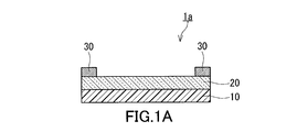
- FIG. 1A is a cross-sectional view showing an example of a heater member of the present invention.
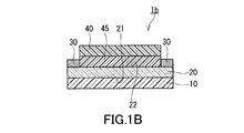
- FIG. 1B is a cross-sectional view showing another example of the heater member of the present invention.
- FIG. 2 is a cross-sectional view showing an example of the heater tape of the present invention.
- FIG. 3 is a cross-sectional view showing an example of a molded member with a heater according to the present invention.
- FIG. 4: is a figure which illustrates notionally the measuring method of the internal stress of a transparent conductive film.
- the present inventors devised the member for heaters concerning the present invention based on the following new knowledge in the process of examination about the heater for maintaining the transparency of a transparent body.
- the temperature of the heating element which is a transparent conductive film
- the heater be able to operate at a high temperature rise rate (eg, 20 ° C./min or more).
- a high temperature rise rate eg, 20 ° C./min or more.
- the transparent conductive film have a low sheet resistance.
- the thickness of the transparent conductive film is large, the sheet resistance of the transparent conductive film is low. Therefore, it is desirable that the thickness of the transparent conductive film is a predetermined value or more.
- the thickness of the transparent conductive film heating element exceeds 20 nm. Is desirable.
- the present inventors newly found that a crack may occur in the transparent conductive film when the heater is operated at a high temperature rising rate. Therefore, the inventors of the present invention conducted repeated studies on a technique capable of preventing the occurrence of a crack in the transparent conductive film when the heater is operated at a high temperature rising rate.
- the transparent conductive film has good durability and generation of cracks even when the heater is operated at a high temperature rise rate. I found new things that I can prevent.
- the heater member 1a includes a support 10, a heating element 20, and at least a pair of power supply electrodes 30.
- the support 10 is made of an organic polymer and is in the form of a sheet.
- the heat generating body 20 is a transparent conductive film which is in contact with one main surface of the support 10 and is made of a polycrystalline body containing indium oxide as a main component.
- At least one pair of power supply electrodes 30 is in contact with one main surface of the heating element 20.
- the heating element 20 has a sheet resistance in the range of 10 to 150 ⁇ / ⁇ .
- the thickness of the heating element 20 is more than 20 nm and 200 nm or less.
- the internal stress of the heating element 20 measured by the X-ray stress measurement method is 500 MPa or less.
- the internal stress generated in the heating element 20 is typically compressive stress.
- the internal stress of the heating element 20 can be measured by the method described in the embodiment according to the X-ray stress measurement method.
- the sheet resistance of the heat generating body 20 can be easily adjusted to 150 ⁇ / ⁇ or less. Since the heating element 20 has a sheet resistance of 150 ⁇ / ⁇ or less, the temperature of the heating element 20 can be raised to a desired temperature in a short time. That is, the heater provided with the member 1a for heaters can be operated at a high temperature rising rate. Moreover, when the thickness of the heat generating body 20 is 200 nm or less, the heater member 1a can be efficiently produced, and the manufacturing cost of the heater member 1a is low.
- the heat generating body 20 when the thickness of the heat generating body 20 is 200 nm or less, the heat generating body 20 is unlikely to be cracked. From the viewpoint of adjusting the thickness of the heating element 20 to 200 nm or less, the sheet resistance of the heating element 20 is 10 ⁇ / ⁇ or more.
- the thickness of the heat generating body 20 is determined as described above, when the internal stress of the heat generating body 20 is 500 MPa or less, a crack is generated in the transparent conductive film even when the heater is operated at a high temperature rising rate. This can be advantageously prevented, and the heater member 1a has good durability.
- the thickness of the heating element 20 is desirably 25 nm or more, and more desirably 27 nm or more.
- the thickness of the heating element 20 is desirably 180 nm or less, and more desirably 170 nm or less.
- the sheet resistance of the heating element 20 is desirably 10 to 80 ⁇ / ⁇ , and more desirably 10 to 60 ⁇ / ⁇ .
- the internal stress of the heating element 20 is desirably 490 MPa or less, and more desirably 480 MPa or less.
- the internal stress of the heating element 20 is associated with true stress and thermal stress.
- the true stress is a stress caused by a defect inside the transparent conductive film generated when forming the transparent conductive film.
- the thermal stress is a stress caused by the temperature condition when forming the transparent conductive film and the difference in the linear expansion coefficient between the support 10 and the film formed on the support 10.
- True stress can be reduced by adjusting the conditions for forming the transparent conductive film (for example, the conditions for sputtering) to reduce defects inside the transparent conductive film.
- the thermal stress can be reduced by adjusting the temperature conditions when forming the transparent conductive film and the dimensional stability of the support 10. Therefore, by appropriately selecting the conditions for forming the transparent conductive film and the material of the support 10, the internal stress of the heating element 20 measured by the X-ray stress measurement method can be 500 MPa or less.
- the support 10 has, for example, the following characteristics.
- the test piece of the support 10 having a width of 4 mm is heated from 25 ° C. to 150 ° C. while being pulled with a force of 0.02 N in a specific direction orthogonal to the width direction.
- the dimensional change rate in a specific direction of the test piece is ⁇ 0.2% to 1%.
- a negative dimensional change rate means that a test piece shrink
- the support 10 needs to be heated to a predetermined temperature, for example, for annealing.
- the internal stress of the transparent conductive film becomes large, and when the heater is operated at a high temperature rising rate, cracks occur in the transparent conductive film. Likely to happen.
- the support 10 since the support 10 has good dimensional stability in the temperature range of 25 ° C. to 150 ° C., the internal stress of the heating element 20 can be easily adjusted to 500 MPa or less.
- the dimensional stability of the heater member 1 a is generally determined by the dimensional stability of the support 10. For example, a test strip having a width of 4 mm not including the pair of electrodes 30 of the heater member 1a is prepared. When the test piece is heated from 25 ° C. to 150 ° C. while being pulled with a force of 0.02 N in a specific direction orthogonal to the width direction, the dimensional change in the specific direction of the test piece is, for example, -0.2% ⁇ 1%. For example, if the support 10 has the above-described dimensional stability in the temperature range of 25 ° C. to 150 ° C., the heater member 1 a also has such dimensional stability in the temperature range of 25 ° C. to 150 ° C.
- light of a predetermined range of wavelength can be transmitted through the heater member 1a.
- light of a wavelength of a predetermined range in the wavelength range of the visible light region and the wavelength range of the near infrared region can be transmitted through the heater member 1a.
- the material of the support 10 is not limited to a specific material as long as the internal stress of the heating element 20 can be adjusted to 500 MPa or less, but the support 10 is desirably polyethylene naphthalate, polyimide, polycarbonate, polyether ether ketone, and It is made of at least one selected from the group consisting of aromatic polyamides. Thereby, the support 10 has good dimensional stability in a temperature range of 25 ° C. to 150 ° C., and the heater member 1 a has desired transparency.
- the support 10 may be provided with a functional layer such as a hard coat layer, a stress relaxation layer, or an optical adjustment layer. These functional layers constitute, for example, one main surface of the support 10 in contact with the heating element 20. These functional layers can be the base of the heating element 20.
- the thickness of the support 10 is not limited to a specific thickness, but is, for example, 10 ⁇ m to 200 ⁇ m from the viewpoint of good transparency, good strength, and easy handling.
- the thickness of the support 10 is desirably 20 ⁇ m to 180 ⁇ m, and more desirably 30 ⁇ m to 160 ⁇ m.
- the heating element 20 has, for example, a specific resistance of 1.5 ⁇ 10 ⁇ 4 to 5.0 ⁇ 10 ⁇ 4 ⁇ ⁇ cm. Thereby, when adjusting the thickness of the heat generating body 20 to the thickness of more than 20 nm and 200 nm or less, the heat generating body 20 tends to have a desired sheet resistance.
- the heating element 20 desirably has a specific resistance of more than 1.5 ⁇ 10 ⁇ 4 ⁇ ⁇ cm and not more than 3.0 ⁇ 10 ⁇ 4 ⁇ ⁇ cm, and more desirably 1.6 ⁇ 10 ⁇ 4 ⁇ ⁇ It has a resistivity of from cm to 2.8 ⁇ 10 -4 ⁇ ⁇ cm.
- the transparent conductive film constituting the heating element 20 is not particularly limited, but is preferably made of indium tin oxide (ITO).
- the feeding electrode 30 has a thickness of, for example, 1 ⁇ m or more. In this case, the current capacity of the power supply electrode 30 is likely to be adjusted to a value suitable for operating the heater at a high temperature rising rate. Thus, when the heater is operated at a high temperature rising rate, the power supply electrode 30 is not easily peeled off.
- the thickness of the power supply electrode 30 is much larger than the thickness of an electrode formed on a transparent conductive film used for a display device such as a touch panel.
- the feeding electrode 30 desirably has a thickness of 1.5 ⁇ m or more, and more desirably has a thickness of 2 ⁇ m or more.
- the feeding electrode 30 has a thickness of, for example, 5 mm or less, may have a thickness of 1 mm or less, and may have a thickness of 700 ⁇ m or less.
- the temperature rising rate of the heating element 20 is, for example, 20 ° C./minute or more.
- the temperature of the heating element 20 can be raised to a desired temperature in a short time.
- the temperature raising rate of the heating element 20 may be 15 ° C./min or more, preferably 25 ° C./min or more, and more preferably 30 ° C./min or more.
- the transparent conductive film is formed, for example, by sputtering using a target material containing indium oxide as a main component to form a thin film derived from the target material on one main surface of the support 10.
- a thin film derived from the target material is formed on one main surface of the support 10 by high magnetic field DC magnetron sputtering.
- the thin film formed on one of the main surfaces of the support 10 is optionally annealed.
- annealing treatment is performed by placing the thin film in the air at 120 ° C. to 150 ° C. for 1 hour to 3 hours. This promotes crystallization of the thin film, and a transparent conductive film made of a polycrystalline body is advantageously formed. If the temperature of the environment of the thin film at the time of the annealing treatment and the time of the annealing treatment fall within the above range, defects are less likely to occur in the transparent conductive film, and the internal stress of the heating element 20 is easily adjusted to 500 MPa or less.
- the pair of feeding electrodes 30 is not particularly limited as long as it can supply power from the power source (not shown) to the heating element 20, but is made of, for example, a metal material.
- a masking film is disposed so as to cover a part of the main surface of heating element 20 located on the opposite side of the main surface of heating element 20 in contact with support 10. When another film is laminated on the main surface of the heating element 20, a masking film may be disposed on the film. In this state, a metal film of 1 ⁇ m or more on the exposed portion of the heating element 20 and the masking film by a dry process such as chemical vapor deposition (CVD) and physical vapor deposition (PVD) or a wet process such as plating.
- CVD chemical vapor deposition
- PVD physical vapor deposition
- the metal film remains on the exposed portion of the heating element 20, and a pair of power feeding electrodes 30 can be formed. Further, a metal film of 1 ⁇ m or more is formed on the main surface of the heat generating body 20 by a dry process such as CVD and PVD or a wet process such as a plating method, and thereafter an unnecessary metal film is removed by etching.
- the power supply electrode 30 may be formed.
- the pair of power supply electrodes 30 may be formed of a conductive paste.
- the pair of feeding electrodes 30 can be formed by applying a conductive paste to the heating element 20 which is a transparent conductive film by a method such as screen printing.
- the heater member 1a can be changed from various viewpoints.
- the heater member 1a may be changed as the heater member 1b shown in FIG. 1B.
- the heater member 1b is configured the same as the heater member 1a except in the case where it is particularly described.
- the constituent elements of the heater member 1b that are the same as or correspond to the constituent elements of the heater member 1a are assigned the same reference numerals, and detailed description thereof is omitted.
- the description of the heater member 1a also applies to the heater member 1b unless technically contradictory.
- the heater member 1 b further includes a protective film 40 and a first adhesive layer 45.
- the protective film 40 is disposed closer to the second major surface 22 than the first major surface 21.
- the first major surface 21 is the major surface of the heating element 20 in contact with the support 10.
- the second major surface 22 is the major surface of the heat generating body 20 located on the opposite side of the first major surface 21.
- the first adhesive layer 45 is in contact with the protective film 40 and the heating element 20 between the protective film 40 and the heating element 20.
- the protective film 40 is attached to the second major surface 22 of the heat generating body 20 via the first adhesive layer 45. Since the heating element 20 is made of a polycrystalline body containing indium oxide as a main component as described above, its toughness is generally low. For this reason, by protecting the heat generating body 20 by the protective film 40, the impact resistance of the heater member 1a can be improved.
- the protective film 40 is not particularly limited as long as it has appropriate transparency, but for example, it is desirable to have good dimensional stability when using the heater member 1a. From this point of view, the protective film 40 desirably has the following characteristics. When a test piece of the protective film 40 having a width of 4 mm is heated from 25 ° C. to 150 ° C. while being pulled with a force of 0.02 N in a specific direction orthogonal to the width direction, the dimensional change of the test piece in the specific direction is -0.2% to 1%. Thereby, the protective film 40 is hard to peel off by the dimensional change of the protective film 40 at the time of use of the member 1a for heaters.
- the protective film 40 is made of, for example, at least one selected from the group consisting of polyethylene naphthalate, polyimide, polycarbonate, polyetheretherketone, and aromatic polyamide. Thereby, the support 10 has good dimensional stability in a temperature range of 25 ° C. to 150 ° C., and the heater member 1 a has desired transparency.
- the thickness of the protective film 40 is not particularly limited, and is, for example, 20 ⁇ m to 200 ⁇ m, preferably 25 ⁇ m to 190 ⁇ m, and more preferably 30 ⁇ m to 180 ⁇ m. Thus, it is possible to prevent the thickness of the heater member 1a from becoming too large while the heater member 1a has good impact resistance.
- the first adhesive layer 45 is formed of, for example, a known optical pressure-sensitive adhesive such as an acrylic pressure-sensitive adhesive.
- the heater tape can be manufactured using the heater member 1a or the heater member 1b.
- the heater tape 2 includes a heater member 1 b, a separator 60, and a second adhesive layer 65.
- the separator 60 is disposed closer to the fourth major surface 14 than the third major surface 13.
- the third major surface 13 is the major surface of the support 10 in contact with the heating element 20.
- the fourth major surface 14 is the major surface of the support 10 located on the opposite side of the third major surface 13.
- the second adhesive layer 65 is in contact with the separator 60 and the support 10 between the separator 60 and the support 10. By peeling off the separator 60, the second adhesive layer 65 is exposed. Thereafter, the heater member 1a can be attached to the adherend by pressing the second adhesive layer 65 against the adherend.
- the heater tape 2 may be changed to include the heater member 1a instead of the heater member 1b.
- the separator 60 is typically a film that can maintain the adhesion of the second adhesive layer 65 when covering the second adhesive layer 65 and can be easily peeled off from the second adhesive layer 65.
- the separator 60 is, for example, a film made of a polyester resin such as polyethylene terephthalate (PET).
- the second adhesive layer 65 is formed of, for example, a known optical pressure-sensitive adhesive such as an acrylic pressure-sensitive adhesive.
- the molded member 3 with a member for a heater can be produced using the member for a heater 1a or the member for a heater 1b.
- the member-attached molded article 3 for a heater includes a member 1 b for a heater, a molded article 80, and a second adhesive layer 65.
- the molded body 80 is disposed closer to the fourth major surface 14 than the third major surface 13.
- the third major surface 13 is the major surface of the support 10 in contact with the heating element 20.
- the fourth major surface 14 is the major surface of the support 10 located on the opposite side of the third major surface 13.
- the second adhesive layer 65 is in contact with the molded body 80 and the support 10 between the molded body 80 and the support 10.
- the member-attached molded body 3 for heater may be changed to include the member 1a for heater instead of the member 1b for heater.
- the molded body 80 is typically a component that transmits light in a specific wavelength range. For example, when deposits such as fog, frost, and snow adhere to the surface of the molded body 80, the light to be transmitted through the molded body 80 is blocked. However, a voltage is applied to the pair of power supply electrodes 30 of the heater member 1b to heat the heat generating body 20 to remove deposits such as fog, frost, and snow attached to the surface of the molded body 80. Thereby, the transparency of the molded member 3 with a heater can be maintained.
- the light to be transmitted through the molded body 80 is not limited to visible light, and may be ultraviolet light or near infrared light.
- the second adhesive layer 65 is formed of, for example, a known optical pressure-sensitive adhesive such as an acrylic pressure-sensitive adhesive.
- the second adhesive layer 65 exposed by peeling off the separator 60 of the heater tape 2 is pressed against the molded body 80 and the heater member 1b is attached to the molded body 80, for example. It can be produced by
- the thickness of the transparent conductive film (heating element) of the heater member according to each example and each comparative example was measured by the X-ray reflectance method using an X-ray diffraction apparatus (product name: RINT 2200, manufactured by RIGAKU Co., Ltd.) . The results are shown in Table 1. Moreover, the X-ray-diffraction pattern with respect to a transparent conductive film was obtained using the X-ray-diffraction apparatus. Cu-K alpha ray was used as X-ray. In all the Examples and all Comparative Examples, it was confirmed from the obtained X-ray diffraction patterns that the transparent conductive film had a polycrystalline structure.
- the edge part of the electrode for electric power feeding formed on the transparent conductive film of the member for heaters which concerns on each Example and each comparative example using a stylus type surface shape measuring instrument (product name: Dektak 8 made by ULVAC, Inc.)
- the thickness of the power supply electrode of the heater member according to each of the examples and the comparative examples was measured by measuring the height of each. The results are shown in Table 1.
- the integration time at each measurement point was set to 100 seconds.
- the ITO crystal lattice spacing d at each measurement angle ( ⁇ ) is calculated from the peak angle 2 ⁇ of the obtained X-ray diffraction (peak of ITO (222) plane) and the wavelength ⁇ of the X-ray irradiated from the light source
- the crystal lattice strain ⁇ was calculated from the crystal lattice spacing d from the relationship of the following formulas (1) and (2).
- ⁇ is the wavelength of the X-ray (Cu-K ⁇ ray) emitted from the light source, and ⁇ is 0.1541 nm.
- the angle ( ⁇ ) between the normal to the main surface of the transparent conductive film sample Sa and the normal to the crystal plane of the ITO crystal Cr is 45 °, 52 °, 60 °, 70 °, and 90
- the above X-ray diffraction measurements were performed to calculate the crystal lattice strain ⁇ at each angle ( ⁇ ).
- the residual stress (internal stress) ⁇ in the in-plane direction of the transparent conductive film was determined by the following formula (3) from the slope of a straight line plotting the relationship between sin 2 ⁇ and crystal lattice strain ⁇ .
- Table 1 ⁇ (1 + ⁇ ) / E ⁇ ⁇ sin 2 ⁇ (2 ⁇ / E) ⁇ (3)
- E is the Young's modulus (116 GPa) of ITO
- ⁇ is a Poisson's ratio (0.35).
- thermomechanical analyzer product name: TMA / SS 6100, manufactured by Hitachi High-Tech Science Co., Ltd.
- the dimensional change of the test piece was measured.
- the width of the test piece was 4 mm.
- the distance between the pair of chucks was 10 mm when the test piece was fixed before the temperature rise.
- a tensile force of 0.02 N was continuously applied to the test piece in the direction orthogonal to the width direction.
- the temperature rising rate of the test piece was set to + 5 ° C./min.
- the dimensional change rate was determined from the following equation (4).
- D 150 is the distance between the chucks when the temperature of the test piece reaches 150 ° C.
- Dimension change rate [%] ⁇ (D 150 ⁇ D i ) / D i ⁇ ⁇ 100 (4)
- the temperature rise rate at the time of electricity supply Using a DC constant voltage power supply manufactured by Kikusui Electronics Co., Ltd., a voltage of 12 V is applied to a pair of feeding electrodes of the heater member according to each example and each comparative example to generate a transparent conductive film (heat generation of the heater member Conductivity test was conducted to apply current to the body. During the current-carrying test, the surface temperature of the transparent conductive film (heating element) or the protective film was measured using a thermograph manufactured by FLIER SYSTEMS CO., LTD., And the temperature rising rate was calculated. The results are shown in Table 1.
- Example 1 Indium tin oxide (ITO) (content of tin oxide: 10% by weight) on one principal surface of a film of polyethylene naphthalate (PEN) (manufactured by Teijin Film Solutions, product name: Theonex) having a thickness of 125 ⁇ m was used as a target material, and the magnetic flux density of the horizontal magnetic field on the surface of the target material was a high magnetic field of 100 mT (milliTesla), and an ITO film was formed by DC magnetron sputtering in the presence of an inert gas. .
- the PEN film was subjected to an annealing treatment in the air at 150 ° C. for 3 hours. Thereby, the ITO was crystallized to form a transparent conductive film.
- the thickness of the transparent conductive film was 115 nm.
- the transparent conductive film obtained by the annealing treatment had a polycrystalline structure.
- the PEN film on which the transparent conductive film is formed is cut into strips (short side: 30 mm ⁇ long side: 50 mm), and a pair of ends of the transparent conductive film extending in the longitudinal direction are exposed while facing each other. As a result, a part of the transparent conductive film was covered with a masking film. Each of the pair of ends had a width of 2 mm.
- a Cu thin film having a thickness of 100 nm was formed on the transparent conductive film and the masking film by DC magnetron sputtering. Furthermore, the Cu thin film was subjected to a wet plating process to increase the thickness of the Cu film to 3 ⁇ m. Thereafter, the masking film was removed, and a pair of feeding electrodes was formed in portions corresponding to the pair of end portions of the transparent conductive film. Thus, a heater member according to Example 1 was produced.
- Example 2 A member for a heater according to Example 2 was produced in the same manner as Example 1, except that a transparent polyimide film (transparent PI, manufactured by Koron Industry Co., Ltd.) having a thickness of 50 ⁇ m was used instead of the PEN film.
- a transparent polyimide film transparent PI, manufactured by Koron Industry Co., Ltd.
- Example 3 A member for a heater according to Example 3 was produced in the same manner as Example 1 except that a polyimide film (PI, manufactured by Toray DuPont, product name: Kapton) having a thickness of 75 ⁇ m was used instead of the PEN film. did.
- PI polyimide film
- Kapton Kapton
- Example 4 A member for a heater according to Example 4 was prepared in the same manner as in Example 1 except that a polycarbonate (PC) film (Sumitomo Chemical Co., product name: Technoloy C000) having a thickness of 125 ⁇ m was used instead of the PEN film. Made.
- PC polycarbonate
- Example 5 A member for a heater according to Example 5 was produced in the same manner as Example 1, except that the conditions of the DC magnetron sputtering method in forming the ITO film were changed such that the thickness of the transparent conductive film was 29 nm.
- Example 6 A member for a heater according to Example 6 was produced in the same manner as Example 1, except that the conditions of the DC magnetron sputtering method in forming the ITO film were changed such that the thickness of the transparent conductive film was 153 nm.
- Example 7 A target of indium tin oxide (ITO) (content ratio of tin oxide: 10% by weight) on one principal surface of a film of polyethylene naphthalate (PEN) (product name: Theonex, manufactured by Teijin Ltd.) having a thickness of 125 ⁇ m
- ITO indium tin oxide
- PEN polyethylene naphthalate
- the magnetic flux density of the horizontal magnetic field on the surface of the target material is a high magnetic field of 100 mT (milliTesla)
- an ITO film is formed by DC magnetron sputtering.
- the PEN film was subjected to an annealing treatment in the air at 150 ° C. for 3 hours. Thereby, the ITO was crystallized to form a transparent conductive film.
- the thickness of the transparent conductive film was 115 nm.
- the transparent conductive film obtained by the annealing treatment had a polycrystalline structure.
- the PEN film on which the transparent conductive film is formed is cut into strips (short side: 30 mm ⁇ long side: 50 mm), and a pair of ends of the transparent conductive film extending in the longitudinal direction are exposed while facing each other. As a result, a part of the transparent conductive film was covered with a masking film. Each of the pair of ends had a width of 2 mm.
- silver paste was screen printed on the transparent conductive film and the masking film. After the print layer of the silver paste was sufficiently cured, the masking film was removed to form a pair of feeding electrodes at portions corresponding to the pair of end portions of the transparent conductive film. The thickness of the feeding electrode was 3 ⁇ m.
- a heater member according to Example 7 was produced.
- Example 8 A member for a heater according to Example 8 was produced in the same manner as Example 1, except that the conditions of the DC magnetron sputtering method in forming the ITO film were changed such that the thickness of the transparent conductive film was 50 nm.
- Example 9 A member for a heater according to Example 9 was produced in the same manner as Example 8, except that the temperature in the annealing treatment of the ITO film was changed to 180 ° C.
- Example 10 A member for a heater according to Example 10 was produced in the same manner as Example 8, except that the conditions of the wet plating process on the Cu thin film were changed such that the thickness of the power supply electrode was 20 ⁇ m.
- Example 11 A planar heater member according to Example 11 was produced in the same manner as Example 1, except that the conditions of the DC magnetron sputtering method in forming the ITO film were changed such that the thickness of the transparent conductive film was 21 nm. .
- Example 12 A planar heater member according to Example 12 was produced in the same manner as Example 1, except that the conditions of the DC magnetron sputtering method in forming the ITO film were changed such that the thickness of the transparent conductive film was 168 nm. .
- Example 13 A target of indium tin oxide (ITO) (content ratio of tin oxide: 10% by weight) on one principal surface of a film of polyethylene naphthalate (PEN) (product name: Theonex, manufactured by Teijin Ltd.) having a thickness of 125 ⁇ m Material, the magnetic flux density of the horizontal magnetic field on the surface of the target material is a high magnetic field of 100 mT (milliTesla), and in the presence of an inert gas, an ITO film 115 nm thick by DC magnetron sputtering It formed.
- the PEN film was subjected to an annealing treatment in the air at 150 ° C. for 3 hours. Thereby, the ITO was crystallized to form a transparent conductive film.
- the transparent conductive film obtained by the annealing treatment had a polycrystalline structure.
- the PEN film on which the transparent conductive film is formed is cut into strips (short side: 30 mm ⁇ long side: 50 mm), and a pair of ends of the transparent conductive film extending in the longitudinal direction are exposed while facing each other.
- a PEN film with adhesive thickness of adhesive layer: 50 ⁇ m, thickness of PEN film (protective film): 50 ⁇ m
- the adhesive-coated PEN film was covered with a masking film, and a Cu thin film having a thickness of 100 nm was formed on the transparent conductive film and the masking film by DC magnetron sputtering.
- the Cu thin film was subjected to a wet plating process to increase the thickness of the Cu film to 3 ⁇ m. Thereafter, the masking film was removed, and a pair of feeding electrodes was formed in portions corresponding to the pair of end portions of the transparent conductive film. Thus, a planar heater member according to Example 13 was produced.
- Comparative Example 1 A member for a heater according to Comparative Example 1 was produced in the same manner as Example 1, except that a biaxially stretched PET film having a thickness of 125 ⁇ m was used instead of the PEN film.
- Comparative Example 2 A member for a heater according to Comparative Example 2 was produced in the same manner as Example 1, except that a polymethyl methacrylate (PMMA) film having a thickness of 125 ⁇ m was used instead of the PEN film.
- PMMA polymethyl methacrylate
- Comparative Example 3 A member for a heater according to Comparative Example 3 was produced in the same manner as Example 1, except that the conditions of the DC magnetron sputtering method in forming the ITO film were changed such that the thickness of the transparent conductive film was 300 nm.
- Comparative Example 4 A member for a heater according to Comparative Example 4 was produced in the same manner as Example 1, except that the conditions of the DC magnetron sputtering method in forming the ITO film were changed such that the thickness of the transparent conductive film was 15 nm.
- Comparative Example 5 A member for a heater according to Comparative Example 1 was produced in the same manner as in Example 8 except that a biaxially stretched PET film having a thickness of 125 ⁇ m was used instead of the PEN film.
- Reference Example 1 A member for a heater according to Reference Example 1 was produced in the same manner as in Example 1 except that the conditions for the wet plating process on the Cu thin film were changed such that the thickness of the feeding electrode was 0.3 ⁇ m.
- Reference Example 2 A member for a heater according to Reference Example 2 was produced in the same manner as in Example 7 except that the conditions for screen printing of silver paste were changed such that the thickness of the power supply electrode was 0.3 ⁇ m.
- the internal stress of the transparent conductive film (heating element) is 500 MPa or less, the dimensional stability of the support in a temperature range of 25 ° C. to 150 ° C. is good, and the thickness of the transparent conductive film is more than 20 nm and 200 nm or less It was suggested that it is important from the viewpoint of preventing the occurrence of cracks in the transparent conductive film when the temperature raising rate of the heating element of the member for heater is high.
- the sheet resistance value of the transparent conductive film is set to 150 ⁇ / sq or less, and the thickness of the feeding electrode is 1 ⁇ m or more. It was suggested that it is desirable to do.
Landscapes
- Surface Heating Bodies (AREA)
Abstract
ヒータ用部材(1a)は、支持体(10)と、発熱体(20)と、少なくとも一対の給電用電極(30)とを備える。支持体(10)は、有機高分子でできたシート状である。発熱体(20)は、支持体(10)の一方の主面に接触している、酸化インジウムを主成分として含有している多結晶体でできている。給電用電極(30)は、発熱体(20)の一方の主面に接触している。発熱体(20)は、10~150Ω/□の範囲内のシート抵抗を有する。発熱体(20)の厚みは、20nmを超え200nm以下である。X線応力測定法によって測定される発熱体(20)の内部応力が500MPa以下である。
Description
本発明は、ヒータ用部材、ヒータ用テープ、及びヒータ用部材付成形体に関する。
従来、透明体の表面を加熱してその表面に付着した霧及び霜を除去する透明な面状のヒータが知られている。
例えば、特許文献1には、ヒータ付透明体が記載されている。このヒータ付透明体において、透明な基材の表面に導電性透明薄膜が形成されている。例えば、ガラス、アクリル樹脂、及びポリエチレン樹脂などでできた基材の表面の全面に、酸化スズ及び酸化インジウム等の導電性透明薄膜が真空蒸着法又はスパッタリング法等の方法で形成される。特許文献1には、給電電極の導電性透明薄膜に対する密着性が低いことが示唆されている。このため、導電性透明薄膜の上にチタン又はチタン合金よりなる層が形成されており、チタン又はチタン合金よりなる層の上に少なくとも一対の給電電極が設けられている。特許文献1によれば、導電性透明薄膜と給電電極との間に、チタン又はチタン合金よりなる層を設けることにより、給電電極の密着性が向上し、給電電極の剥離が防止される。
特許文献1によれば、ヒータ付透明体において、導電性透明薄膜と給電電極との間に、チタン又はチタン合金よりなる層を設けることにより、給電電極の剥離が防止される。一方、特許文献1において、ヒータの昇温速度と導電性透明薄膜の耐久性との関係は具体的に検討されていない。
そこで、本発明は、高い昇温速度で動作可能なヒータを構成するのに有利な耐久性を有するヒータ用部材を提供する。また、本発明は、このようなヒータ用部材を備えた、ヒータ用テープ及びヒータ用部材付成形体を提供する。
本発明は、
有機高分子でできたシート状の支持体と、
前記支持体の一方の主面に接触している、酸化インジウムを主成分として含有している多結晶体でできた透明導電膜である発熱体と、
前記発熱体の一方の主面に接触している少なくとも一対の給電用電極と、を備え、
前記発熱体は、10~150Ω/□の範囲内のシート抵抗を有し、
前記発熱体の厚みは、20nmを超え200nm以下であり、
X線応力測定法によって測定される前記発熱体の内部応力が500MPa以下である、
ヒータ用部材を提供する。
有機高分子でできたシート状の支持体と、
前記支持体の一方の主面に接触している、酸化インジウムを主成分として含有している多結晶体でできた透明導電膜である発熱体と、
前記発熱体の一方の主面に接触している少なくとも一対の給電用電極と、を備え、
前記発熱体は、10~150Ω/□の範囲内のシート抵抗を有し、
前記発熱体の厚みは、20nmを超え200nm以下であり、
X線応力測定法によって測定される前記発熱体の内部応力が500MPa以下である、
ヒータ用部材を提供する。
また、本発明は、
上記のヒータ用部材と、
前記発熱体が接触している前記支持体の主面である第三主面よりも、前記第三主面の反対側に位置する前記支持体の主面である第四主面の近くに配置されたセパレータと、 前記セパレータと前記支持体との間で、前記セパレータ及び前記支持体に接触している第二粘着層と、備えた、
ヒータ用テープを提供する。
上記のヒータ用部材と、
前記発熱体が接触している前記支持体の主面である第三主面よりも、前記第三主面の反対側に位置する前記支持体の主面である第四主面の近くに配置されたセパレータと、 前記セパレータと前記支持体との間で、前記セパレータ及び前記支持体に接触している第二粘着層と、備えた、
ヒータ用テープを提供する。
また、本発明は、
上記のヒータ用部材と、
前記発熱体が接触している前記支持体の主面である第三主面よりも、前記第三主面の反対側に位置する前記支持体の主面である第四主面の近くに配置された成形体と、
前記成形体と前記支持体との間で、前記成形体及び前記支持体に接触している第二粘着層と、を備えた、
ヒータ用部材付成形体を提供する。
上記のヒータ用部材と、
前記発熱体が接触している前記支持体の主面である第三主面よりも、前記第三主面の反対側に位置する前記支持体の主面である第四主面の近くに配置された成形体と、
前記成形体と前記支持体との間で、前記成形体及び前記支持体に接触している第二粘着層と、を備えた、
ヒータ用部材付成形体を提供する。
上記のヒータ用部材は、高い昇温速度で動作可能なヒータを構成するのに有利な耐久性を有する。
本発明者らは、透明体の透明性を保つためのヒータに関する検討の過程で、下記の新たな知見に基づいて本発明に係るヒータ用部材を案出した。
ヒータにおいて、透明体の透明性を損なう霧、霜、及び雪等の付着物を早期に取り除くために、透明導電膜である発熱体の温度が短期間に所望の温度まで上昇することが望ましい。すなわち、ヒータが高い昇温速度(例えば、20℃/分以上)で動作可能であることが望ましい。このため、透明導電膜が低いシート抵抗を有することが望ましい。透明導電膜の厚みが大きいと、透明導電膜のシート抵抗は低くなるので、透明導電膜の厚みが所定値以上であることが望ましい。本発明者らの検討によれば、ヒータが高い昇温速度で動作可能なように透明導電膜のシート抵抗を低くするためには、透明導電膜である発熱体の厚みは20nmを超えていることが望ましい。一方で、本発明者らは、高い昇温速度でヒータを動作させた場合に透明導電膜にクラックが発生する場合があることを新たに見出した。そこで、本発明者らは、高い昇温速度でヒータを動作させた場合に透明導電膜においてクラックの発生を防止できる技術について日夜検討を重ねた。その結果、透明導電膜の内部応力(圧縮応力)を特定の範囲に調整することにより、高い昇温速度でヒータを動作させた場合でも透明導電膜が良好な耐久性を有しクラックの発生を防止できることを新たに見出した。
以下、本発明の実施形態について、図面を参照しながら説明する。なお、下記の説明は、本発明を例示的に説明するものであり、本発明は以下の実施形態に限定されるわけではない。
図1Aに示す通り、ヒータ用部材1aは、支持体10と、発熱体20と、少なくとも一対の給電用電極30とを備えている。支持体10は、有機高分子でできており、シート状である。発熱体20は、支持体10の一方の主面に接触しており、酸化インジウムを主成分として含有している多結晶体でできた透明導電膜である。少なくとも一対の給電用電極30は、発熱体20の一方の主面に接触している。発熱体20は、10~150Ω/□の範囲内のシート抵抗を有する。発熱体20の厚みは、20nmを超え200nm以下である。また、X線応力測定法によって測定される発熱体20の内部応力が500MPa以下である。発熱体20に発生する内部応力は典型的には圧縮応力である。発熱体20の内部応力は、X線応力測定法に従って実施例に記載の方法で測定できる。
ヒータ用部材1aにおいて、発熱体20の厚みが20nmを超えていると、発熱体20のシート抵抗を150Ω/□以下に調整しやすい。発熱体20が150Ω/□以下のシート抵抗を有することにより、発熱体20の温度を所望の温度まで短期間に上昇させることができる。すなわち、ヒータ用部材1aを備えたヒータを高い昇温速度で動作させることができる。また、発熱体20の厚みが200nm以下であると、ヒータ用部材1aを効率良く生産でき、ヒータ用部材1aの製造コストが低い。加えて、発熱体20の厚みが200nm以下であると、発熱体20にクラックが発生しにくい。発熱体20の厚みを200nm以下に調整する観点から、発熱体20のシート抵抗は10Ω/□以上である。
発熱体20の厚みが上記のように定められたうえで、発熱体20の内部応力が500MPa以下であると、高い昇温速度でヒータを動作させても透明導電膜においてクラックが発生することを有利に防止でき、ヒータ用部材1aが良好な耐久性を有する。
発熱体20の厚みは、望ましくは25nm以上であり、より望ましくは27nm以上である。発熱体20の厚みは、望ましくは180nm以下であり、より望ましくは170nm以下である。
発熱体20のシート抵抗は、望ましくは10~80Ω/□であり、より望ましくは10~60Ω/□である。
発熱体20の内部応力は、望ましくは490MPa以下であり、より望ましくは480MPa以下である。
発熱体20の内部応力には、真応力及び熱応力が関連している。真応力は、透明導電膜を形成するときに発生した透明導電膜の内部の欠陥に起因する応力である。熱応力は、透明導電膜を形成するときの温度条件及び支持体10と支持体10に形成された膜との間の線膨張係数の差に起因する応力である。真応力は、透明導電膜を形成する条件(例えば、スパッタリングの条件)を調節して透明導電膜の内部の欠陥を少なくすることにより低減できる。熱応力は、透明導電膜を形成するときの温度条件及び支持体10の寸法安定性を調節することにより低減できる。このため、透明導電膜を形成する条件及び支持体10の材料を適切に選択することにより、X線応力測定法によって測定される発熱体20の内部応力を500MPa以下にできる。
支持体10は、例えば以下の特性を有する。4mmの幅を有する支持体10の試験片を幅方向と直交する特定方向に0.02Nの力で引っ張りながら25℃から150℃まで加熱する。このとき、この試験片の特定方向における寸法変化率が-0.2%~1%である。なお、負の寸法変化率は、試験片が収縮することを意味する。支持体10に透明導電膜を形成する場合、例えば、アニール処理等のために、支持体10を所定の温度に加熱する必要がある。この場合、仮に、支持体10の加熱及び冷却に伴う寸法変化が大きいと、透明導電膜の内部応力が大きくなってしまい、高い昇温速度でヒータを動作させた場合に透明導電膜においてクラックが発生しやすい。しかし、支持体10は、上記の通り、25℃から150℃の温度範囲において、良好な寸法安定性を有するので、発熱体20の内部応力を500MPa以下に調節しやすい。
ヒータ用部材1aの寸法安定性は、概ね、支持体10の寸法安定性によって決まる。例えば、ヒータ用部材1aの一対の電極30を含まない4mmの幅の試験片を準備する。この試験片を幅方向と直交する特定方向に0.02Nの力で引っ張りながら25℃から150℃まで加熱したときに、この試験片の特定方向における寸法変化率が、例えば、-0.2%~1%である。例えば、支持体10が25℃から150℃の温度範囲において上記の寸法安定性を有していれば、ヒータ用部材1aも25℃から150℃の温度範囲においてこのような寸法安定性を有する。
典型的には、所定の範囲の波長の光がヒータ用部材1aを透過できる。例えば、可視光領域の波長範囲及び近赤外線領域の波長範囲における所定の範囲の波長の光がヒータ用部材1aを透過できる。
支持体10の材料は、発熱体20の内部応力を500MPa以下に調節できる限り特定の材料に制限されないが、支持体10は、望ましくは、ポリエチレンナフタレート、ポリイミド、ポリカーボネート、ポリエーテルエーテルケトン、及び芳香族ポリアミドからなる群から選ばれる少なくとも1つでできている。これにより、支持体10が25℃から150℃の温度範囲において良好な寸法安定性を有し、かつ、ヒータ用部材1aが所望の透明性を有する。
支持体10は、ハードコート層、応力緩和層、又は光学調整層等の機能層を備えていてもよい。これらの機能層は、例えば、発熱体20と接触する支持体10の一方の主面をなしている。これらの機能層は、発熱体20の下地でありうる。
支持体10の厚みは、特定の厚みに制限されないが、良好な透明性、良好な強度、及び取り扱い易さの観点から、例えば、10μm~200μmである。支持体10の厚みは、望ましくは20μm~180μmであり、より望ましくは30μm~160μmである。
発熱体20は、例えば、1.5×10⁻⁴~5.0×10⁻⁴Ω・cmの比抵抗を有する。これにより、20nmを超え200nm以下の厚みに発熱体20の厚みを調整する場合に、発熱体20が所望のシート抵抗を有しやすい。発熱体20は、望ましくは、1.5×10⁻⁴Ω・cmを超え3.0×10⁻⁴Ω・cm以下の比抵抗を有し、より望ましくは1.6×10⁻⁴Ω・cm~2.8×10⁻⁴Ω・cmの比抵抗を有する。
発熱体20を構成する透明導電膜は、特に制限されないが、望ましくは酸化インジウムスズ(ITO)によってできている。
給電用電極30は、例えば、1μm以上の厚みを有する。この場合、給電用電極30における電流容量がヒータを高い昇温速度で動作させるのに適した値に調整されやすい。これにより、ヒータを高い昇温速度で動作させる場合に、給電用電極30が剥離しにくい。なお、この給電用電極30の厚みは、タッチパネル等の表示デバイスに使用される透明導電性フィルムに形成される電極の厚みに比べると格段に大きい。給電用電極30は、望ましくは1.5μm以上の厚みを有し、より望ましくは2μm以上の厚みを有する。給電用電極30は、例えば5mm以下の厚みを有し、1mm以下の厚みを有していてもよく、700μm以下の厚みを有していてもよい。
ヒータ用部材1aにおいて、一対の給電用電極30に12Vの直流電圧を加えた場合、発熱体20の昇温速度は、例えば、20℃/分以上である。このように、発熱体20の温度を所望の温度まで短期間に上昇させることができる。一対の給電用電極30に12Vの直流電圧を加えた場合、発熱体20の昇温速度は、15℃/分以上であってもよいが、望ましくは25℃/分以上であり、より望ましくは30℃/分以上である。
透明導電膜は、例えば、酸化インジウムを主成分として含有しているターゲット材を用いてスパッタリングを行い、支持体10の一方の主面にターゲット材に由来する薄膜を形成することにより形成される。望ましくは、高磁場DCマグネトロンスパッタ法によって、支持体10の一方の主面にターゲット材に由来する薄膜が形成される。これにより、透明導電膜の中に欠陥が発生しにくく、発熱体20の内部応力を500MPa以下に調節しやすい。
支持体10の一方の主面に形成された薄膜は、必要に応じて、アニール処理される。例えば、120℃~150℃の大気中に、薄膜を1時間~3時間置いてアニール処理がなされる。これにより、薄膜の結晶化が促され、多結晶体でできた透明導電膜が有利に形成される。アニール処理時の薄膜の環境の温度及びアニール処理の時間が上記の範囲あれば、透明導電膜の中に欠陥が発生しにくく、発熱体20の内部応力を500MPa以下に調節しやすい。
一対の給電用電極30は、発熱体20に電源(図示省略)からの電力を供給できる限り、特に制限されないが、例えば、金属材料でできている。支持体10と接触している発熱体20の主面の反対側に位置する発熱体20の主面の一部を覆うようにマスキングフィルムを配置する。発熱体20の主面上に別のフィルムが積層されている場合には、そのフィルムの上にマスキングフィルムを配置してもよい。この状態で、化学気相成長法(CVD)及び物理気相成長法(PVD)等のドライプロセス又はメッキ法等のウェットプロセスにより、発熱体20の露出部及びマスキングフィルム上に1μm以上の金属膜を形成する。その後、マスキングフィルムを取り除くことにより、発熱体20の露出部上に金属膜が残り、一対の給電用電極30を形成できる。また、CVD及びPVD等のドライプロセス又はメッキ法等のウェットプロセスにより、発熱体20の主面上に1μm以上の金属膜を形成し、その後、不要な金属膜をエッチングにより除去して、一対の給電用電極30を形成してもよい。
一対の給電用電極30は、導電性ペーストによって形成されてもよい。この場合、透明導電膜である発熱体20に導電性ペーストをスクリーン印刷等の方法によって塗布することによって一対の給電用電極30を形成できる。
(変形例)
ヒータ用部材1aは、様々な観点から変更可能である。例えば、ヒータ用部材1aは、図1Bに示すヒータ用部材1bのように変更されてもよい。ヒータ用部材1bは、特に説明する場合を除き、ヒータ用部材1aと同様に構成されている。ヒータ用部材1aの構成要素と同一又は対応するヒータ用部材1bの構成要素には、同一の符号を付し、詳細な説明を省略する。ヒータ用部材1aに関する説明は、技術的に矛盾しない限り、ヒータ用部材1bにも当てはまる。
ヒータ用部材1aは、様々な観点から変更可能である。例えば、ヒータ用部材1aは、図1Bに示すヒータ用部材1bのように変更されてもよい。ヒータ用部材1bは、特に説明する場合を除き、ヒータ用部材1aと同様に構成されている。ヒータ用部材1aの構成要素と同一又は対応するヒータ用部材1bの構成要素には、同一の符号を付し、詳細な説明を省略する。ヒータ用部材1aに関する説明は、技術的に矛盾しない限り、ヒータ用部材1bにも当てはまる。
図1Bに示す通り、ヒータ用部材1bは、保護フィルム40と、第一粘着層45とをさらに備えている。保護フィルム40は、第一主面21よりも第二主面22の近くに配置されている。第一主面21は、支持体10と接触している発熱体20の主面である。第二主面22は、第一主面21の反対側に位置する発熱体20の主面である。第一粘着層45は、保護フィルム40と発熱体20との間で、保護フィルム40及び発熱体20に接触している。このように、保護フィルム40が第一粘着層45を介して発熱体20の第二主面22に貼り付けられている。発熱体20は、上記の通り、酸化インジウムを主成分として含有している多結晶体でできているので、その靭性は一般的に低い。このため、保護フィルム40によって発熱体20を保護することによって、ヒータ用部材1aの耐衝撃性を高めることができる。
保護フィルム40は、適切な透明性を有する限り特に制限されないが、例えば、ヒータ用部材1aの使用時に良好な寸法安定性を有することが望ましい。この観点から、保護フィルム40は、望ましくは、下記の特性を有する。4mmの幅を有する保護フィルム40の試験片を幅方向と直交する特定方向に0.02Nの力で引っ張りながら25℃から150℃まで加熱したときに、この試験片の特定方向における寸法変化率が-0.2%~1%である。これにより、ヒータ用部材1aの使用時における保護フィルム40の寸法変化によって保護フィルム40が剥離しにくい。
保護フィルム40は、例えば、ポリエチレンナフタレート、ポリイミド、ポリカーボネート、ポリエーテルエーテルケトン、及び芳香族ポリアミドからなる群から選ばれる少なくとも1つでできている。これにより、支持体10が25℃から150℃の温度範囲において良好な寸法安定性を有し、かつ、ヒータ用部材1aが所望の透明性を有する。保護フィルム40の厚みは、特に制限されないが、例えば20μm~200μmであり、望ましくは25μm~190μmであり、より望ましくは30μm~180μmである。これにより、ヒータ用部材1aが良好な耐衝撃性を有しつつヒータ用部材1aの厚みが大きくなりすぎることを防止できる。
第一粘着層45は、例えば、アクリル系粘着剤等の公知の光学用粘着剤によって形成されている。
(ヒータ用テープ)
ヒータ用部材1a又はヒータ用部材1bを用いて、ヒータ用テープを作製できる。図2に示す通り、ヒータ用テープ2は、ヒータ用部材1bと、セパレータ60と、第二粘着層65とを備えている。セパレータ60は、第三主面13よりも、第四主面14の近くに配置されている。第三主面13は、発熱体20が接触している支持体10の主面である。第四主面14は、第三主面13の反対側に位置する支持体10の主面である。第二粘着層65は、セパレータ60と支持体10との間で、セパレータ60及び支持体10に接触している。セパレータ60を剥離することにより第二粘着層65が露出する。その後、第二粘着層65を被着材に押圧することにより、ヒータ用部材1aを被着材に貼り付けることができる。ヒータ用テープ2は、ヒータ用部材1bに代えて、ヒータ用部材1aを備えるように変更されてもよい。
ヒータ用部材1a又はヒータ用部材1bを用いて、ヒータ用テープを作製できる。図2に示す通り、ヒータ用テープ2は、ヒータ用部材1bと、セパレータ60と、第二粘着層65とを備えている。セパレータ60は、第三主面13よりも、第四主面14の近くに配置されている。第三主面13は、発熱体20が接触している支持体10の主面である。第四主面14は、第三主面13の反対側に位置する支持体10の主面である。第二粘着層65は、セパレータ60と支持体10との間で、セパレータ60及び支持体10に接触している。セパレータ60を剥離することにより第二粘着層65が露出する。その後、第二粘着層65を被着材に押圧することにより、ヒータ用部材1aを被着材に貼り付けることができる。ヒータ用テープ2は、ヒータ用部材1bに代えて、ヒータ用部材1aを備えるように変更されてもよい。
セパレータ60は、典型的には、第二粘着層65を覆っているときに第二粘着層65の粘着力を保つことができ、かつ、第二粘着層65から容易に剥離できるフィルムである。セパレータ60は、例えば、ポリエチレンテレフタレート(PET)等のポリエステル樹脂製のフィルムである。
第二粘着層65は、例えば、アクリル系粘着剤等の公知の光学用粘着剤によって形成されている。
(ヒータ用部材付成形体)
ヒータ用部材1a又はヒータ用部材1bを用いて、ヒータ用部材付成形体3を作製できる。図3に示す通り、ヒータ用部材付成形体3は、ヒータ用部材1bと、成形体80と、第二粘着層65とを備えている。成形体80は、第三主面13よりも第四主面14の近くに配置されている。第三主面13は、発熱体20が接触している支持体10の主面である。第四主面14は、第三主面13の反対側に位置する支持体10の主面である。第二粘着層65は、成形体80と支持体10との間で、成形体80及び支持体10に接触している。ヒータ用部材付成形体3は、ヒータ用部材1bに代えて、ヒータ用部材1aを備えるように変更されてもよい。
ヒータ用部材1a又はヒータ用部材1bを用いて、ヒータ用部材付成形体3を作製できる。図3に示す通り、ヒータ用部材付成形体3は、ヒータ用部材1bと、成形体80と、第二粘着層65とを備えている。成形体80は、第三主面13よりも第四主面14の近くに配置されている。第三主面13は、発熱体20が接触している支持体10の主面である。第四主面14は、第三主面13の反対側に位置する支持体10の主面である。第二粘着層65は、成形体80と支持体10との間で、成形体80及び支持体10に接触している。ヒータ用部材付成形体3は、ヒータ用部材1bに代えて、ヒータ用部材1aを備えるように変更されてもよい。
成形体80は、典型的には、特定の波長範囲の光を透過させる部品である。例えば、成形体80の表面に霧、霜、及び雪等の付着物が付着すると、成形体80を透過すべき光が遮られてしまう。しかし、ヒータ用部材1bの一対の給電用電極30に電圧を加えて発熱体20を発熱させて成形体80の表面に付着した、霧、霜、及び雪等の付着物を除去できる。これにより、ヒータ用部材付成形体3の透明性を保つことができる。なお、成形体80を透過すべき光は、可視光に限られず、紫外光又は近赤外光でありうる。
第二粘着層65は、例えば、アクリル系粘着剤等の公知の光学用粘着剤によって形成されている。
ヒータ用部材付成形体3は、例えば、ヒータ用テープ2のセパレータ60を剥離して露出した第二粘着層65を成形体80に押圧して、ヒータ用部材1bを成形体80に貼り付けることによって作製できる。
以下、実施例により本発明をより詳細に説明する。なお、本発明は以下の実施例に限定されない。まず、各実施例及び各比較例に関する評価方法及び測定方法について説明する。
[厚み測定]
X線回折装置(リガク社製、製品名:RINT2200)を用いて、X線反射率法によって、各実施例及び各比較例に係るヒータ用部材の透明導電膜(発熱体)の厚みを測定した。結果を表1に示す。また、X線回折装置を用いて、透明導電膜に対するX線回折パターンを得た。X線としてはCu‐Kα線を用いた。すべての実施例及びすべての比較例において、得られたX線回折パターンから透明導電膜が多結晶構造であることを確認した。また、触針式表面形状測定器(ULVAC社製、製品名:Dektak8)を用いて、各実施例及び各比較例に係るヒータ用部材の透明導電膜上に形成された給電用電極の端部の高さを計測することで、各実施例及び各比較例に係るヒータ用部材の給電用電極の厚みを測定した。結果を表1に示す。
X線回折装置(リガク社製、製品名:RINT2200)を用いて、X線反射率法によって、各実施例及び各比較例に係るヒータ用部材の透明導電膜(発熱体)の厚みを測定した。結果を表1に示す。また、X線回折装置を用いて、透明導電膜に対するX線回折パターンを得た。X線としてはCu‐Kα線を用いた。すべての実施例及びすべての比較例において、得られたX線回折パターンから透明導電膜が多結晶構造であることを確認した。また、触針式表面形状測定器(ULVAC社製、製品名:Dektak8)を用いて、各実施例及び各比較例に係るヒータ用部材の透明導電膜上に形成された給電用電極の端部の高さを計測することで、各実施例及び各比較例に係るヒータ用部材の給電用電極の厚みを測定した。結果を表1に示す。
[シート抵抗及び比抵抗]
非接触式抵抗測定装置(ナプソン社製、製品名:NC-80MAP)を用いて、日本工業規格(JIS)Z 2316-1:2014に準拠して、渦電流測定法によって各実施例及び各比較例に係るヒータ用部材の透明導電膜(発熱体)のシート抵抗を測定した。結果を表1に示す。加えて、厚み測定により得られた透明導電膜(発熱体)の厚みと、透明導電膜(発熱体)のシート抵抗との積を求めて、各実施例及び各比較例に係るヒータ用部材の透明導電膜(発熱体)の比抵抗を決定した。結果を表1に示す。
非接触式抵抗測定装置(ナプソン社製、製品名:NC-80MAP)を用いて、日本工業規格(JIS)Z 2316-1:2014に準拠して、渦電流測定法によって各実施例及び各比較例に係るヒータ用部材の透明導電膜(発熱体)のシート抵抗を測定した。結果を表1に示す。加えて、厚み測定により得られた透明導電膜(発熱体)の厚みと、透明導電膜(発熱体)のシート抵抗との積を求めて、各実施例及び各比較例に係るヒータ用部材の透明導電膜(発熱体)の比抵抗を決定した。結果を表1に示す。
[内部応力]
X線回折装置(リガク社製、製品名:RINT2200)を用いて、40kV及び40mAの光源からCu‐Kα線(波長λ:0.1541nm)を平行ビーム光学系を通過させて試料に照射し、sin2Ψ法の原理で透明導電膜の内部応力(圧縮応力)を評価した。sin2Ψ法は、多結晶薄膜の結晶格子歪みの角度(Ψ)に対する依存性から、薄膜の内部応力を求める手法である。上記のX線回折装置を用い、Θ/2Θスキャン測定によって、2θ=29.8°~31.2°の範囲において0.02°おきに回折強度を測定した。各測定点における積算時間は100秒に設定した。得られたX線回折(ITOの(222)面のピーク)のピーク角2θと、光源から照射されたX線の波長λとから、各測定角度(Ψ)におけるITO結晶格子面間隔dを算出し、結晶格子面間隔dから下記の式(1)及び式(2)の関係から結晶格子歪みεを算出した。λは、光源から照射されたX線(Cu‐Kα線)の波長であり、λ=0.1541nmである。d0は、無応力状態のITOの格子面間隔であり、d0=0.2910nmである。d0の値は、International Centre for Diffraction Data (ICDD)のデータベースに記載された値である。
2dsinθ=λ (1)
ε=(d-d0)/d0 (2)
図4に示す通り、透明導電膜の試料Saの主面に対する法線とITO結晶Crの結晶面の法線とのなす角度(Ψ)が45°、52°、60°、70°、及び90°であるそれぞれに場合において、上記のX線回折測定を行い、それぞれの角度(Ψ)における結晶格子歪みεを算出した。その後、透明導電膜の面内方向の残留応力(内部応力)σを、sin2Ψと結晶格子歪みεとの関係をプロットした直線の傾きから下記式(3)により求めた。結果を表1に示す。
ε={(1+ν)/E}σsin2Ψ-(2ν/E)σ (3)
ε={(1+ν)/E}σsin2Ψ-(2ν/E)σ (3)
上記の式(3)において、EはITOのヤング率(116GPa)であり、νはポアソン比(0.35)である。これらの値は、D.G.Neerinck and T.J.Vink, “Depth Profiling of thin ITO films by grazing incidence X-ray diffraction”, Thin Solid Films,278(1996),P12-17 に記載されている値である。図4において、検出器100は、X線回折を検出する。
[支持体の寸法変化の評価]
熱機械分析装置(日立ハイテクサイエンス社製、製品名:TMA/SS6100)を用いて、実施例及び比較例に係るヒータ用部材の支持体の試験片の温度を25℃から150℃まで昇温させたときの試験片の寸法変化率を測定した。試験片の幅は4mmであった。昇温前に試験片を固定したときの一対のチャック間の距離は10mmであった。試験片には幅方向と直交する方向に0.02Nの引っ張り力を加え続けた。この測定において、試験片の昇温速度は、+5℃/分に設定した。以下の式(4)から寸法変化率を求めた。結果を表1に示す。D150は、試験片の温度が150℃になった時のチャック間の距離である。Diは、昇温開始時のチャック間の距離であり、Di=10mmである。
寸法変化率[%]={(D150-Di)/Di}×100 (4)
[通電時の昇温速度]
菊水電子工業社製の直流定電圧電源を用いて、各実施例及び各比較例に係るヒータ用部材の一対の給電用電極に12Vの電圧を印加して、ヒータ用部材の透明導電膜(発熱体)に電流を流す通電試験を行った。通電試験の期間中に、フリアーシステムズ社製のサーモグラフィを用いて、透明導電膜(発熱体)又は保護フィルムの表面温度を測定し、昇温速度を算出した。結果を表1に示す。
菊水電子工業社製の直流定電圧電源を用いて、各実施例及び各比較例に係るヒータ用部材の一対の給電用電極に12Vの電圧を印加して、ヒータ用部材の透明導電膜(発熱体)に電流を流す通電試験を行った。通電試験の期間中に、フリアーシステムズ社製のサーモグラフィを用いて、透明導電膜(発熱体)又は保護フィルムの表面温度を測定し、昇温速度を算出した。結果を表1に示す。
[透明導電膜におけるクラックの確認]
上記の通電試験の期間中に透明導電膜にクラックが発生するか否かを目視により確認した。結果を表1に示す。表1において、「N」との表記はクラックが発生していなかったことを意味し、「Y」との表記はクラックが発生していたことを意味する。
上記の通電試験の期間中に透明導電膜にクラックが発生するか否かを目視により確認した。結果を表1に示す。表1において、「N」との表記はクラックが発生していなかったことを意味し、「Y」との表記はクラックが発生していたことを意味する。
上記の通電試験の期間中に給電用電極及び透明導電膜の剥離が発生するか否かを目視により確認した。結果を表1に示す。表1において、「N」との表記は給電用電極及び透明導電膜の剥離が発生しなかったことを意味し、「Y」との表記は給電用電極及び透明導電膜の剥離が発生したことを意味する。
<実施例1>
125μmの厚みを有するポリエチレンナフタレート(PEN)のフィルム(帝人フィルムソリューション社製、製品名:テオネックス)の一方の主面上に、酸化インジウムスズ(ITO)(酸化スズの含有率:10重量%)をターゲット材として用いて、当該ターゲット材の表面での水平磁場の磁束密度が100mT(ミリテスラ)の高磁場であり、不活性ガスが存在する状態において、DCマグネトロンスパッタ法により、ITO膜を形成した。ITO膜を形成した後のPENフィルムを、150℃の大気中に3時間置いて、アニール処理を行った。これにより、ITOを結晶化させ、透明導電膜を形成した。透明導電膜の厚みは115nmであった。アニール処理によって得られた透明導電膜は多結晶構造であった。
125μmの厚みを有するポリエチレンナフタレート(PEN)のフィルム(帝人フィルムソリューション社製、製品名:テオネックス)の一方の主面上に、酸化インジウムスズ(ITO)(酸化スズの含有率:10重量%)をターゲット材として用いて、当該ターゲット材の表面での水平磁場の磁束密度が100mT(ミリテスラ)の高磁場であり、不活性ガスが存在する状態において、DCマグネトロンスパッタ法により、ITO膜を形成した。ITO膜を形成した後のPENフィルムを、150℃の大気中に3時間置いて、アニール処理を行った。これにより、ITOを結晶化させ、透明導電膜を形成した。透明導電膜の厚みは115nmであった。アニール処理によって得られた透明導電膜は多結晶構造であった。
次に、透明導電膜が形成されたPENフィルムを短冊状(短辺:30mm×長辺:50mm)に切り出し、互いに対向しつつ長手方向に延びている透明導電膜の一対の端部が露出するようにマスキングフィルムで透明導電膜の一部を覆った。一対の端部のそれぞれは2mmの幅を有していた。この状態で、透明導電膜及びマスキングフィルムの上に、100nmの厚みを有するCu薄膜をDCマグネトロンスパッタ法により形成した。さらに、Cu薄膜に対して、湿式めっき処理を行い、Cuの膜の厚みを3μmまで増加させた。その後、マスキングフィルムを除去して、透明導電膜の一対の端部に相当する部分に一対の給電用電極を形成した。このようにして、実施例1に係るヒータ用部材を作製した。
<実施例2>
PENフィルムの代わりに、50μmの厚みを有する透明ポリイミドフィルム(透明PI、コーロンインダストリー社製)を用いた以外は実施例1と同様にして、実施例2に係るヒータ用部材を作製した。
PENフィルムの代わりに、50μmの厚みを有する透明ポリイミドフィルム(透明PI、コーロンインダストリー社製)を用いた以外は実施例1と同様にして、実施例2に係るヒータ用部材を作製した。
<実施例3>
PENフィルムの代わりに、75μmの厚みを有するポリイミドフィルム(PI、東レ・デュポン社製、製品名:カプトン)を用いた以外は実施例1と同様にして、実施例3に係るヒータ用部材を作製した。
PENフィルムの代わりに、75μmの厚みを有するポリイミドフィルム(PI、東レ・デュポン社製、製品名:カプトン)を用いた以外は実施例1と同様にして、実施例3に係るヒータ用部材を作製した。
<実施例4>
PENフィルムの代わりに、125μmの厚みを有するポリカーボネート(PC)フィルム(住友化学社製、製品名:テクノロイC000)を用いた以外は実施例1と同様にして、実施例4に係るヒータ用部材を作製した。
PENフィルムの代わりに、125μmの厚みを有するポリカーボネート(PC)フィルム(住友化学社製、製品名:テクノロイC000)を用いた以外は実施例1と同様にして、実施例4に係るヒータ用部材を作製した。
<実施例5>
透明導電膜の厚みが29nmになるようにITO膜の形成におけるDCマグネトロンスパッタ法の条件を変更した以外は、実施例1と同様にして、実施例5に係るヒータ用部材を作製した。
透明導電膜の厚みが29nmになるようにITO膜の形成におけるDCマグネトロンスパッタ法の条件を変更した以外は、実施例1と同様にして、実施例5に係るヒータ用部材を作製した。
<実施例6>
透明導電膜の厚みが153nmになるように、ITO膜の形成におけるDCマグネトロンスパッタ法の条件を変更した以外は、実施例1と同様にして、実施例6に係るヒータ用部材を作製した。
透明導電膜の厚みが153nmになるように、ITO膜の形成におけるDCマグネトロンスパッタ法の条件を変更した以外は、実施例1と同様にして、実施例6に係るヒータ用部材を作製した。
<実施例7>
125μmの厚みを有するポリエチレンナフタレート(PEN)のフィルム(帝人社製、製品名:テオネックス)の一方の主面上に、酸化インジウムスズ(ITO)(酸化スズの含有率:10重量%)をターゲット材として用いて、当該ターゲット材の表面での水平磁場の磁束密度が100mT(ミリテスラ)の高磁場であり、不活性ガスが存在する状態において、DCマグネトロンスパッタ法により、ITO膜を形成した。ITO膜を形成した後のPENフィルムを、150℃の大気中に3時間置いて、アニール処理を行った。これにより、ITOを結晶化させ、透明導電膜を形成した。透明導電膜の厚みは115nmであった。アニール処理によって得られた透明導電膜は多結晶構造であった。
125μmの厚みを有するポリエチレンナフタレート(PEN)のフィルム(帝人社製、製品名:テオネックス)の一方の主面上に、酸化インジウムスズ(ITO)(酸化スズの含有率:10重量%)をターゲット材として用いて、当該ターゲット材の表面での水平磁場の磁束密度が100mT(ミリテスラ)の高磁場であり、不活性ガスが存在する状態において、DCマグネトロンスパッタ法により、ITO膜を形成した。ITO膜を形成した後のPENフィルムを、150℃の大気中に3時間置いて、アニール処理を行った。これにより、ITOを結晶化させ、透明導電膜を形成した。透明導電膜の厚みは115nmであった。アニール処理によって得られた透明導電膜は多結晶構造であった。
次に、透明導電膜が形成されたPENフィルムを短冊状(短辺:30mm×長辺:50mm)に切り出し、互いに対向しつつ長手方向に延びている透明導電膜の一対の端部が露出するようにマスキングフィルムで透明導電膜の一部を覆った。一対の端部のそれぞれは2mmの幅を有していた。この状態で、透明導電膜及びマスキングフィルムの上に、銀ペーストをスクリーン印刷した。銀ペーストの印刷層が十分に硬化した後、マスキングフィルムを除去して、透明導電膜の一対の端部に相当する部分に一対の給電用電極を形成した。給電用電極の厚みは3μmであった。このようにして、実施例7に係るヒータ用部材を作製した。
<実施例8>
透明導電膜の厚みが50nmになるように、ITO膜の形成におけるDCマグネトロンスパッタ法の条件を変更した以外は、実施例1と同様にして、実施例8に係るヒータ用部材を作製した。
透明導電膜の厚みが50nmになるように、ITO膜の形成におけるDCマグネトロンスパッタ法の条件を変更した以外は、実施例1と同様にして、実施例8に係るヒータ用部材を作製した。
<実施例9>
ITO膜のアニール処理における温度を180℃に変更した以外は、実施例8と同様にして、実施例9に係るヒータ用部材を作製した。
ITO膜のアニール処理における温度を180℃に変更した以外は、実施例8と同様にして、実施例9に係るヒータ用部材を作製した。
<実施例10>
給電用電極の厚みが20μmになるように、Cu薄膜に対する湿式めっき処理の条件を変更した以外は、実施例8と同様にして、実施例10に係るヒータ用部材を作製した。
給電用電極の厚みが20μmになるように、Cu薄膜に対する湿式めっき処理の条件を変更した以外は、実施例8と同様にして、実施例10に係るヒータ用部材を作製した。
<実施例11>
透明導電膜の厚みが21nmになるように、ITO膜の形成におけるDCマグネトロンスパッタ法の条件を変更した以外は、実施例1と同様にして、実施例11に係る面状ヒータ用部材を作製した。
透明導電膜の厚みが21nmになるように、ITO膜の形成におけるDCマグネトロンスパッタ法の条件を変更した以外は、実施例1と同様にして、実施例11に係る面状ヒータ用部材を作製した。
<実施例12>
透明導電膜の厚みが168nmになるように、ITO膜の形成におけるDCマグネトロンスパッタ法の条件を変更した以外は、実施例1と同様にして、実施例12に係る面状ヒータ用部材を作製した。
透明導電膜の厚みが168nmになるように、ITO膜の形成におけるDCマグネトロンスパッタ法の条件を変更した以外は、実施例1と同様にして、実施例12に係る面状ヒータ用部材を作製した。
<実施例13>
125μmの厚みを有するポリエチレンナフタレート(PEN)のフィルム(帝人社製、製品名:テオネックス)の一方の主面上に、酸化インジウムスズ(ITO)(酸化スズの含有率:10重量%)をターゲット材として用いて、当該ターゲット材の表面での水平磁場の磁束密度が100mT(ミリテスラ)の高磁場であり、不活性ガスが存在する状態において、DCマグネトロンスパッタ法により、115nmの厚みのITO膜を形成した。ITO膜を形成した後のPENフィルムを、150℃の大気中に3時間置いて、アニール処理を行った。これにより、ITOを結晶化させ、透明導電膜を形成した。アニール処理によって得られた透明導電膜は多結晶構造であった。
125μmの厚みを有するポリエチレンナフタレート(PEN)のフィルム(帝人社製、製品名:テオネックス)の一方の主面上に、酸化インジウムスズ(ITO)(酸化スズの含有率:10重量%)をターゲット材として用いて、当該ターゲット材の表面での水平磁場の磁束密度が100mT(ミリテスラ)の高磁場であり、不活性ガスが存在する状態において、DCマグネトロンスパッタ法により、115nmの厚みのITO膜を形成した。ITO膜を形成した後のPENフィルムを、150℃の大気中に3時間置いて、アニール処理を行った。これにより、ITOを結晶化させ、透明導電膜を形成した。アニール処理によって得られた透明導電膜は多結晶構造であった。
次に、透明導電膜が形成されたPENフィルムを短冊状(短辺:30mm×長辺:50mm)に切り出し、互いに対向しつつ長手方向に延びている透明導電膜の一対の端部が露出するように粘着剤付PENフィルム(粘着剤層の厚み:50μm、PENフィルム(保護フィルム)の厚み:50μm)を透明導電膜の一部に貼り付けた。一対の端部のそれぞれは2mmの幅を有していた。さらに、粘着剤付PENフィルムをマスキングフィルムで覆い、透明導電膜及びマスキングフィルムの上に、100nmの厚みを有するCu薄膜をDCマグネトロンスパッタ法により形成した。さらに、Cu薄膜に対して、湿式めっき処理を行い、Cuの膜の厚みを3μmまで増加させた。その後、マスキングフィルムを除去して、透明導電膜の一対の端部に相当する部分に一対の給電用電極を形成した。このようにして、実施例13に係る面状ヒータ用部材を作製した。
<比較例1>
PENフィルムの代わりに、125μmの厚みを有する2軸延伸PETフィルムを用いた以外は、実施例1と同様にして、比較例1に係るヒータ用部材を作製した。
PENフィルムの代わりに、125μmの厚みを有する2軸延伸PETフィルムを用いた以外は、実施例1と同様にして、比較例1に係るヒータ用部材を作製した。
<比較例2>
PENフィルムの代わりに、125μmの厚みを有するポリメタクリル酸メチル(PMMA)フィルムを用いた以外は、実施例1と同様にして、比較例2に係るヒータ用部材を作製した。
PENフィルムの代わりに、125μmの厚みを有するポリメタクリル酸メチル(PMMA)フィルムを用いた以外は、実施例1と同様にして、比較例2に係るヒータ用部材を作製した。
<比較例3>
透明導電膜の厚みが300nmになるように、ITO膜の形成におけるDCマグネトロンスパッタ法の条件を変更した以外は、実施例1と同様にして、比較例3に係るヒータ用部材を作製した。
透明導電膜の厚みが300nmになるように、ITO膜の形成におけるDCマグネトロンスパッタ法の条件を変更した以外は、実施例1と同様にして、比較例3に係るヒータ用部材を作製した。
<比較例4>
透明導電膜の厚みが15nmになるように、ITO膜の形成におけるDCマグネトロンスパッタ法の条件を変更した以外は、実施例1と同様にして、比較例4に係るヒータ用部材を作製した。
透明導電膜の厚みが15nmになるように、ITO膜の形成におけるDCマグネトロンスパッタ法の条件を変更した以外は、実施例1と同様にして、比較例4に係るヒータ用部材を作製した。
<比較例5>
PENフィルムの代わりに、125μmの厚みを有する2軸延伸PETフィルムを用いた以外は、実施例8と同様にして、比較例1に係るヒータ用部材を作製した。
PENフィルムの代わりに、125μmの厚みを有する2軸延伸PETフィルムを用いた以外は、実施例8と同様にして、比較例1に係るヒータ用部材を作製した。
<参考例1>
給電用電極の厚みが0.3μmになるように、Cu薄膜に対する湿式めっき処理の条件を変更した以外は、実施例1と同様にして、参考例1に係るヒータ用部材を作製した。
給電用電極の厚みが0.3μmになるように、Cu薄膜に対する湿式めっき処理の条件を変更した以外は、実施例1と同様にして、参考例1に係るヒータ用部材を作製した。
<参考例2>
給電用電極の厚みが0.3μmになるように、銀ペーストのスクリーン印刷の条件を変更した以外は、実施例7と同様にして、参考例2に係るヒータ用部材を作製した。
給電用電極の厚みが0.3μmになるように、銀ペーストのスクリーン印刷の条件を変更した以外は、実施例7と同様にして、参考例2に係るヒータ用部材を作製した。
表1に示す通り、比較例1~3、5に係るヒータ用部材の通電試験において、透明導電膜にクラックが発生することが確認された。比較例1、2、及び5に係るヒータ用部材の透明導電膜は500MPaを超える内部応力(圧縮応力)を有しており、25℃から150℃の温度範囲における支持体の寸法安定性も良好であるとは言い難かった。比較例3に係るヒータ用部材の透明導電膜の厚みは300nmであった。これに対し、実施例1~13に係るヒータ用部材の通電試験において、透明導電膜にクラックが発生しないことが確認された。透明導電膜(発熱体)の内部応力が500MPa以下であること、25℃から150℃の温度範囲における支持体の寸法安定性が良好であること、及び透明導電膜の厚みが20nmを超え200nm以下であることが、ヒータ用部材の発熱体の昇温速度が高い場合に透明導電膜にクラックが発生することを防止する観点から、重要であることが示唆された。
表1に示す通り、比較例4に係るヒータ用部材の通電試験において、透明導電膜にクラックは発生しなかったものの、透明導電膜の昇温速度は20℃/分未満(8℃/分)であった。比較例4に係るヒータ用部材において、透明導電膜のシート抵抗が高いためにこのような低い昇温速度が測定されたと考えられる。このため、比較例4に係るヒータ用部材は短期間で透明導電膜の温度を所望の温度まで上昇させることが難しいことが示唆された。これに対し、実施例1~13に係るヒータ用部材の通電試験において、透明導電膜の昇温速度は20℃/分を超えていた。参考例1及び2に係るヒータ用部材の通電試験において、給電用電極及び透明導電膜の剥離並びに透明導電膜におけるクラックは発生しなかったが、透明導電膜の昇温速度は15℃/分であった。これらの結果を踏まえると、短期間で透明導電膜の温度を所望の温度まで上昇させるために、透明導電膜のシート抵抗値を150Ω/□以下に設定し、給電用電極の厚みを1μm以上にすることが望ましいことが示唆された。

Claims (9)
- 有機高分子でできたシート状の支持体と、
前記支持体の一方の主面に接触している、酸化インジウムを主成分として含有している多結晶体でできた透明導電膜である発熱体と、
前記発熱体の一方の主面に接触している少なくとも一対の給電用電極と、を備え、
前記発熱体は、10~150Ω/□の範囲内のシート抵抗を有し、
前記発熱体の厚みは、20nmを超え200nm以下であり、
X線応力測定法によって測定される前記発熱体の内部応力が500MPa以下である、
ヒータ用部材。 - 4mmの幅を有する前記支持体の試験片を幅方向と直交する特定方向に0.02Nの力で引っ張りながら25℃から150℃まで加熱したときに、前記試験片の前記特定方向における寸法変化率が-0.2%~1%である、請求項1に記載のヒータ用部材。
- 当該ヒータ用部材の前記一対の電極を含まない4mmの幅の試験片を幅方向と直交する特定方向に0.02Nの力で引っ張りながら25℃から150℃まで加熱したときに、前記試験片の前記特定方向における寸法変化率が-0.2%~1%である、請求項1に記載のヒータ用部材。
- 前記支持体は、ポリエチレンナフタレート、ポリイミド、ポリカーボネート、ポリエーテルエーテルケトン、及び芳香族ポリアミドからなる群から選ばれる少なくとも1つでできている、請求項1~3のいずれか1項に記載のヒータ用部材。
- 前記発熱体は、1.5×10⁻⁴~5.0×10⁻⁴Ω・cmの比抵抗を有する、請求項1~4のいずれか1項に記載のヒータ用部材。
- 前記給電用電極は、1μm以上の厚みを有する、請求項1~5のいずれか1項に記載のヒータ部材。
- 前記支持体と接触している前記発熱体の主面である第一主面よりも、前記第一主面の反対側に位置する前記発熱体の主面である第二主面の近くに配置された保護フィルムと、
前記保護フィルムと前記発熱体との間で、前記保護フィルム及び前記発熱体に接触している第一粘着層と、をさらに備えた、
請求項1~6のいずれか1項に記載のヒータ用部材。 - 請求項1~7のいずれか1項に記載のヒータ用部材と、
前記発熱体が接触している前記支持体の主面である第三主面よりも、前記第三主面の反対側に位置する前記支持体の主面である第四主面の近くに配置されたセパレータと、
前記セパレータと前記支持体との間で、前記セパレータ及び前記支持体に接触している第二粘着層と、備えた、
ヒータ用テープ。 - 請求項1~7のいずれか1項に記載のヒータ用部材と、
前記発熱体が接触している前記支持体の主面である第三主面よりも、前記第三主面の反対側に位置する前記支持体の主面である第四主面の近くに配置された成形体と、
前記成形体と前記支持体との間で、前記成形体及び前記支持体に接触している第二粘着層と、を備えた、
ヒータ用部材付成形体。
Priority Applications (4)
| Application Number | Priority Date | Filing Date | Title |
|---|---|---|---|
| KR1020207004174A KR20200038251A (ko) | 2017-08-04 | 2018-08-03 | 히터용 부재, 히터용 테이프 및 히터용 부재 부착 성형체 |
| EP18842042.6A EP3664577B1 (en) | 2017-08-04 | 2018-08-03 | Heater member, heater tape, and molded body equipped with heater member |
| CN201880050702.7A CN110999533B (zh) | 2017-08-04 | 2018-08-03 | 加热器用构件、加热器用胶带、以及带有加热器用构件的成形体 |
| US16/636,149 US11589426B2 (en) | 2017-08-04 | 2018-08-03 | Heater member, heater tape, and molded body equipped with heater member |
Applications Claiming Priority (4)
| Application Number | Priority Date | Filing Date | Title |
|---|---|---|---|
| JP2017-152002 | 2017-08-04 | ||
| JP2017152002 | 2017-08-04 | ||
| JP2018-145549 | 2018-08-02 | ||
| JP2018145549A JP7162461B2 (ja) | 2017-08-04 | 2018-08-02 | ヒータ用部材、ヒータ用テープ、及びヒータ用部材付成形体 |
Publications (1)
| Publication Number | Publication Date |
|---|---|
| WO2019027048A1 true WO2019027048A1 (ja) | 2019-02-07 |
Family
ID=65232848
Family Applications (1)
| Application Number | Title | Priority Date | Filing Date |
|---|---|---|---|
| PCT/JP2018/029292 WO2019027048A1 (ja) | 2017-08-04 | 2018-08-03 | ヒータ用部材、ヒータ用テープ、及びヒータ用部材付成形体 |
Country Status (1)
| Country | Link |
|---|---|
| WO (1) | WO2019027048A1 (ja) |
Cited By (1)
| Publication number | Priority date | Publication date | Assignee | Title |
|---|---|---|---|---|
| CN112578364A (zh) * | 2019-09-27 | 2021-03-30 | 丰田合成株式会社 | 近红外传感器罩 |
Citations (6)
| Publication number | Priority date | Publication date | Assignee | Title |
|---|---|---|---|---|
| JPS61175068U (ja) * | 1985-04-22 | 1986-10-31 | ||
| JPS63115048U (ja) * | 1987-01-16 | 1988-07-25 | ||
| JPH0963754A (ja) * | 1995-06-15 | 1997-03-07 | Mitsui Toatsu Chem Inc | 耐久性透明面状ヒーター及びその製造方法 |
| JPH09125236A (ja) * | 1995-10-30 | 1997-05-13 | Hitachi Metals Ltd | インジウム酸化物系焼結体およびその製造方法ならびにインジウム酸化物系ターゲット |
| JP2002134254A (ja) | 2000-10-30 | 2002-05-10 | Pentel Corp | ヒーター付透明体 |
| JP2007220636A (ja) * | 2006-02-20 | 2007-08-30 | Nissei Electric Co Ltd | 透明導電膜ヒータ |
-
2018
- 2018-08-03 WO PCT/JP2018/029292 patent/WO2019027048A1/ja unknown
Patent Citations (6)
| Publication number | Priority date | Publication date | Assignee | Title |
|---|---|---|---|---|
| JPS61175068U (ja) * | 1985-04-22 | 1986-10-31 | ||
| JPS63115048U (ja) * | 1987-01-16 | 1988-07-25 | ||
| JPH0963754A (ja) * | 1995-06-15 | 1997-03-07 | Mitsui Toatsu Chem Inc | 耐久性透明面状ヒーター及びその製造方法 |
| JPH09125236A (ja) * | 1995-10-30 | 1997-05-13 | Hitachi Metals Ltd | インジウム酸化物系焼結体およびその製造方法ならびにインジウム酸化物系ターゲット |
| JP2002134254A (ja) | 2000-10-30 | 2002-05-10 | Pentel Corp | ヒーター付透明体 |
| JP2007220636A (ja) * | 2006-02-20 | 2007-08-30 | Nissei Electric Co Ltd | 透明導電膜ヒータ |
Non-Patent Citations (2)
| Title |
|---|
| D. G. NEERINCKT. J. VINK: "Depth Profiling of thin ITO films by grazing incidence X-ray diffraction", THIN SOLID FILMS, vol. 278, 1996, pages 12 - 17 |
| See also references of EP3664577A4 * |
Cited By (1)
| Publication number | Priority date | Publication date | Assignee | Title |
|---|---|---|---|---|
| CN112578364A (zh) * | 2019-09-27 | 2021-03-30 | 丰田合成株式会社 | 近红外传感器罩 |
Similar Documents
| Publication | Publication Date | Title |
|---|---|---|
| JP5543907B2 (ja) | 透明導電性フィルムおよびその製造方法 | |
| WO2019027049A1 (ja) | ヒータ | |
| JP6600550B2 (ja) | 金属層積層透明導電性フィルムおよびそれを用いたタッチセンサ | |
| JP7162461B2 (ja) | ヒータ用部材、ヒータ用テープ、及びヒータ用部材付成形体 | |
| WO2022091829A1 (ja) | 透明導電圧電フィルムおよびタッチパネル | |
| WO2019027048A1 (ja) | ヒータ用部材、ヒータ用テープ、及びヒータ用部材付成形体 | |
| WO2020203133A1 (ja) | ヒータ | |
| WO2020026898A1 (ja) | ヒータ及びヒータ付物品 | |
| US20220341024A1 (en) | Transparent conductive film, laminate, and method for producing transparent conductive film | |
| JP7176879B2 (ja) | ヒータ | |
| CN111696702A (zh) | 薄膜层叠体、及图案化导电性薄膜的制造方法 | |
| US20210345457A1 (en) | Heater and article equipped with heater | |
| KR20240019750A (ko) | 투명 도전성 필름 | |
| JP2020167106A (ja) | ヒータ |
Legal Events
| Date | Code | Title | Description |
|---|---|---|---|
| 121 | Ep: the epo has been informed by wipo that ep was designated in this application |
Ref document number: 18842042 Country of ref document: EP Kind code of ref document: A1 |
|
| NENP | Non-entry into the national phase |
Ref country code: DE |
|
| ENP | Entry into the national phase |
Ref document number: 20207004174 Country of ref document: KR Kind code of ref document: A |
|
| ENP | Entry into the national phase |
Ref document number: 2018842042 Country of ref document: EP Effective date: 20200304 |