WO2019011071A1 - 薄膜晶体管的制备方法、薄膜晶体管、阵列基板和显示面板 - Google Patents
薄膜晶体管的制备方法、薄膜晶体管、阵列基板和显示面板 Download PDFInfo
- Publication number
- WO2019011071A1 WO2019011071A1 PCT/CN2018/088872 CN2018088872W WO2019011071A1 WO 2019011071 A1 WO2019011071 A1 WO 2019011071A1 CN 2018088872 W CN2018088872 W CN 2018088872W WO 2019011071 A1 WO2019011071 A1 WO 2019011071A1
- Authority
- WO
- WIPO (PCT)
- Prior art keywords
- layer
- gate
- substrate
- conductor
- insulating layer
- Prior art date
- Legal status (The legal status is an assumption and is not a legal conclusion. Google has not performed a legal analysis and makes no representation as to the accuracy of the status listed.)
- Ceased
Links
Images





Classifications
-
- H—ELECTRICITY
- H10—SEMICONDUCTOR DEVICES; ELECTRIC SOLID-STATE DEVICES NOT OTHERWISE PROVIDED FOR
- H10D—INORGANIC ELECTRIC SEMICONDUCTOR DEVICES
- H10D86/00—Integrated devices formed in or on insulating or conducting substrates, e.g. formed in silicon-on-insulator [SOI] substrates or on stainless steel or glass substrates
- H10D86/01—Manufacture or treatment
- H10D86/021—Manufacture or treatment of multiple TFTs
- H10D86/0231—Manufacture or treatment of multiple TFTs using masks, e.g. half-tone masks
-
- H—ELECTRICITY
- H10—SEMICONDUCTOR DEVICES; ELECTRIC SOLID-STATE DEVICES NOT OTHERWISE PROVIDED FOR
- H10D—INORGANIC ELECTRIC SEMICONDUCTOR DEVICES
- H10D30/00—Field-effect transistors [FET]
- H10D30/01—Manufacture or treatment
- H10D30/021—Manufacture or treatment of FETs having insulated gates [IGFET]
- H10D30/031—Manufacture or treatment of FETs having insulated gates [IGFET] of thin-film transistors [TFT]
-
- H—ELECTRICITY
- H10—SEMICONDUCTOR DEVICES; ELECTRIC SOLID-STATE DEVICES NOT OTHERWISE PROVIDED FOR
- H10D—INORGANIC ELECTRIC SEMICONDUCTOR DEVICES
- H10D30/00—Field-effect transistors [FET]
- H10D30/01—Manufacture or treatment
- H10D30/021—Manufacture or treatment of FETs having insulated gates [IGFET]
- H10D30/031—Manufacture or treatment of FETs having insulated gates [IGFET] of thin-film transistors [TFT]
- H10D30/0312—Manufacture or treatment of FETs having insulated gates [IGFET] of thin-film transistors [TFT] characterised by the gate electrodes
- H10D30/0314—Manufacture or treatment of FETs having insulated gates [IGFET] of thin-film transistors [TFT] characterised by the gate electrodes of lateral top-gate TFTs comprising only a single gate
-
- H—ELECTRICITY
- H10—SEMICONDUCTOR DEVICES; ELECTRIC SOLID-STATE DEVICES NOT OTHERWISE PROVIDED FOR
- H10D—INORGANIC ELECTRIC SEMICONDUCTOR DEVICES
- H10D30/00—Field-effect transistors [FET]
- H10D30/01—Manufacture or treatment
- H10D30/021—Manufacture or treatment of FETs having insulated gates [IGFET]
- H10D30/031—Manufacture or treatment of FETs having insulated gates [IGFET] of thin-film transistors [TFT]
- H10D30/0321—Manufacture or treatment of FETs having insulated gates [IGFET] of thin-film transistors [TFT] comprising silicon, e.g. amorphous silicon or polysilicon
-
- H—ELECTRICITY
- H10—SEMICONDUCTOR DEVICES; ELECTRIC SOLID-STATE DEVICES NOT OTHERWISE PROVIDED FOR
- H10D—INORGANIC ELECTRIC SEMICONDUCTOR DEVICES
- H10D30/00—Field-effect transistors [FET]
- H10D30/01—Manufacture or treatment
- H10D30/021—Manufacture or treatment of FETs having insulated gates [IGFET]
- H10D30/031—Manufacture or treatment of FETs having insulated gates [IGFET] of thin-film transistors [TFT]
- H10D30/0321—Manufacture or treatment of FETs having insulated gates [IGFET] of thin-film transistors [TFT] comprising silicon, e.g. amorphous silicon or polysilicon
- H10D30/0323—Manufacture or treatment of FETs having insulated gates [IGFET] of thin-film transistors [TFT] comprising silicon, e.g. amorphous silicon or polysilicon comprising monocrystalline silicon
-
- H—ELECTRICITY
- H10—SEMICONDUCTOR DEVICES; ELECTRIC SOLID-STATE DEVICES NOT OTHERWISE PROVIDED FOR
- H10D—INORGANIC ELECTRIC SEMICONDUCTOR DEVICES
- H10D30/00—Field-effect transistors [FET]
- H10D30/60—Insulated-gate field-effect transistors [IGFET]
- H10D30/67—Thin-film transistors [TFT]
-
- H—ELECTRICITY
- H10—SEMICONDUCTOR DEVICES; ELECTRIC SOLID-STATE DEVICES NOT OTHERWISE PROVIDED FOR
- H10D—INORGANIC ELECTRIC SEMICONDUCTOR DEVICES
- H10D30/00—Field-effect transistors [FET]
- H10D30/60—Insulated-gate field-effect transistors [IGFET]
- H10D30/67—Thin-film transistors [TFT]
- H10D30/6704—Thin-film transistors [TFT] having supplementary regions or layers in the thin films or in the insulated bulk substrates for controlling properties of the device
- H10D30/6713—Thin-film transistors [TFT] having supplementary regions or layers in the thin films or in the insulated bulk substrates for controlling properties of the device characterised by the properties of the source or drain regions, e.g. compositions or sectional shapes
-
- H—ELECTRICITY
- H10—SEMICONDUCTOR DEVICES; ELECTRIC SOLID-STATE DEVICES NOT OTHERWISE PROVIDED FOR
- H10D—INORGANIC ELECTRIC SEMICONDUCTOR DEVICES
- H10D30/00—Field-effect transistors [FET]
- H10D30/60—Insulated-gate field-effect transistors [IGFET]
- H10D30/67—Thin-film transistors [TFT]
- H10D30/6729—Thin-film transistors [TFT] characterised by the electrodes
-
- H—ELECTRICITY
- H10—SEMICONDUCTOR DEVICES; ELECTRIC SOLID-STATE DEVICES NOT OTHERWISE PROVIDED FOR
- H10D—INORGANIC ELECTRIC SEMICONDUCTOR DEVICES
- H10D30/00—Field-effect transistors [FET]
- H10D30/60—Insulated-gate field-effect transistors [IGFET]
- H10D30/67—Thin-film transistors [TFT]
- H10D30/6729—Thin-film transistors [TFT] characterised by the electrodes
- H10D30/673—Thin-film transistors [TFT] characterised by the electrodes characterised by the shapes, relative sizes or dispositions of the gate electrodes
-
- H—ELECTRICITY
- H10—SEMICONDUCTOR DEVICES; ELECTRIC SOLID-STATE DEVICES NOT OTHERWISE PROVIDED FOR
- H10D—INORGANIC ELECTRIC SEMICONDUCTOR DEVICES
- H10D30/00—Field-effect transistors [FET]
- H10D30/60—Insulated-gate field-effect transistors [IGFET]
- H10D30/67—Thin-film transistors [TFT]
- H10D30/6757—Thin-film transistors [TFT] characterised by the structure of the channel, e.g. transverse or longitudinal shape or doping profile
-
- H—ELECTRICITY
- H10—SEMICONDUCTOR DEVICES; ELECTRIC SOLID-STATE DEVICES NOT OTHERWISE PROVIDED FOR
- H10D—INORGANIC ELECTRIC SEMICONDUCTOR DEVICES
- H10D86/00—Integrated devices formed in or on insulating or conducting substrates, e.g. formed in silicon-on-insulator [SOI] substrates or on stainless steel or glass substrates
- H10D86/40—Integrated devices formed in or on insulating or conducting substrates, e.g. formed in silicon-on-insulator [SOI] substrates or on stainless steel or glass substrates characterised by multiple TFTs
-
- H—ELECTRICITY
- H10—SEMICONDUCTOR DEVICES; ELECTRIC SOLID-STATE DEVICES NOT OTHERWISE PROVIDED FOR
- H10D—INORGANIC ELECTRIC SEMICONDUCTOR DEVICES
- H10D86/00—Integrated devices formed in or on insulating or conducting substrates, e.g. formed in silicon-on-insulator [SOI] substrates or on stainless steel or glass substrates
- H10D86/40—Integrated devices formed in or on insulating or conducting substrates, e.g. formed in silicon-on-insulator [SOI] substrates or on stainless steel or glass substrates characterised by multiple TFTs
- H10D86/60—Integrated devices formed in or on insulating or conducting substrates, e.g. formed in silicon-on-insulator [SOI] substrates or on stainless steel or glass substrates characterised by multiple TFTs wherein the TFTs are in active matrices
-
- H—ELECTRICITY
- H10—SEMICONDUCTOR DEVICES; ELECTRIC SOLID-STATE DEVICES NOT OTHERWISE PROVIDED FOR
- H10D—INORGANIC ELECTRIC SEMICONDUCTOR DEVICES
- H10D99/00—Subject matter not provided for in other groups of this subclass
Definitions
- the present disclosure relates to the field of display technologies, and in particular, to a method of fabricating a thin film transistor, a thin film transistor, an array substrate, and a display panel.
- Thin film transistors are very important components in the field of display technology.
- a bottom gate type thin film transistor and a top gate type thin film transistor.
- the gate electrode does not overlap with the source/drain electrodes, so the parasitic capacitance is very low, and the fabrication process of the top-gate thin film transistor is simple, the width-to-length ratio of the channel is larger than W/L, and the layout is flexible. Therefore, it has been widely used in high resolution, high refresh rate, narrow frame, low power consumption products.
- the top-gate thin film transistors currently produced still have problems of low on-state current and high power consumption.
- Embodiments of the present disclosure provide a method of fabricating a thin film transistor, the method comprising:
- Forming source and drain electrodes respectively electrically connected to the conductor regions of the active layer
- the projection of the gate on the substrate is within a projection of the non-conductor region on the substrate, and a projection of the gate and a projection of the two conductor regions on the substrate The distance is between 0 microns and 1 micron.
- the method includes:
- the both sides of the homogeneous active material layer are subjected to a conductor treatment using the gate insulating layer as a mask to obtain the active layer.
- the projection of the gate and the projection of the two conductor regions on the substrate are between 0.1 microns and 0.9 microns, respectively.
- the projection of the gate and the projection of the two conductor regions on the substrate are between 0.1 microns and 0.5 microns, respectively.
- the narrowing the patterned photoresist layer comprises hard baking the patterned photoresist layer.
- the temperature of the hard baking is 130 ° C or higher.
- the narrowing the patterned photoresist layer comprises ashing the patterned photoresist layer.
- the method includes:
- the both sides of the homogeneous active material layer are subjected to a conductor treatment using the gate insulating layer as a mask to obtain the active layer.
- the method includes:
- the gate is formed on the gate insulating layer.
- the method further includes:
- a photoresist is ashed to remove the photoresist of the partially exposed region
- Both sides of the homogeneous active material layer are subjected to a conductor treatment using the remaining photoresist as a mask to obtain the active layer.
- the embodiment of the present disclosure also provides a thin film transistor prepared by the above method.
- the projection of the gate and the projection of the two conductor regions on the substrate are between 0.1 and 1 micron, respectively.
- the projection of the gate and the projection of the two conductor regions on the substrate are between 0.1 and 0.9 microns, respectively.
- the projection of the gate and the projection of the two conductor regions on the substrate are respectively between 0.1 and 0.5 microns.
- Embodiments of the present disclosure also provide an array substrate including the above-described thin film transistor.
- Embodiments of the present disclosure also provide a display panel including the above array substrate.
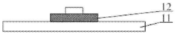
- FIG. 1 is a schematic structural view of a related art in which a homogeneous active layer is formed.
- FIG. 2 is a schematic structural view of the gate electrode of FIG. 1.
- FIG. 2 is a schematic structural view of the gate electrode of FIG. 1.
- FIG. 3 is a schematic structural view of the gate insulating layer of FIG. 2.
- FIG. 3 is a schematic structural view of the gate insulating layer of FIG. 2.
- FIG. 4 is a schematic view showing the structure of the homogeneous active layer in FIG. 3 after being conductorized.
- FIG. 5 is a schematic structural view of the source electrode and the drain electrode formed in FIG. 4.
- FIG. 5 is a schematic structural view of the source electrode and the drain electrode formed in FIG. 4.
- FIG. 6 is a schematic flow diagram of a portion of a method of fabricating a thin film transistor according to some embodiments of the present disclosure.
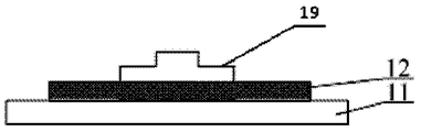
- Figure 7 is a schematic view showing the structure after forming a homogeneous active material layer in some embodiments of the present disclosure.
- FIG. 8 is a schematic structural view of the gate electrode of FIG. 7.
- FIG. 8 is a schematic structural view of the gate electrode of FIG. 7.
- FIG. 9 is a schematic structural view of the photoresist layer in FIG. 8 after hard baking or ashing treatment.
- FIG. 10 is a schematic structural view of the gate insulating layer of FIG. 9.
- FIG. 10 is a schematic structural view of the gate insulating layer of FIG. 9.
- FIG. 11 is a schematic view showing the structure of the active layer in FIG.
- FIG. 12 is a schematic view showing the structure of the interlayer insulating layer in FIG.
- FIG. 13 is a schematic view showing the structure of the source electrode and the drain electrode in FIG.
- FIG. 14 is a schematic structural view of a patterned photoresist layer in another embodiment of the present disclosure.
- FIG. 15 is a schematic view showing the structure of the gate electrode and the gate insulating layer in FIG.
- Fig. 16 is a structural schematic view showing the active layer in Fig. 15 after being conductorized.
- Figure 17 is a schematic view showing the structure of removing a fully exposed region and exposing a portion of the active layer material film in other embodiments of the present disclosure.
- FIG. 18 is a schematic structural view of the active layer material film after etching in FIG. 17.
- FIG. 18 is a schematic structural view of the active layer material film after etching in FIG. 17.
- FIG. 19 is a schematic view showing the structure of the photoresist in FIG. 18 after ashing.
- FIG. 20 is a schematic view showing the structure of the active layer in FIG. 19 after conductor layer removal and removal of the photoresist layer.
- FIG. 20 is a schematic view showing the structure of the active layer in FIG. 19 after conductor layer removal and removal of the photoresist layer.
- FIG. 21 is a schematic view showing the structure of the gate electrode and the gate insulating layer in FIG.
- the low power consumption of the top-gate thin film transistor is mainly affected by the on-state current, and the on-state current is mainly determined by the on-state resistance between the source electrode and the drain electrode.
- the inventors of the present application have found that the top gate type thin film transistor of the related art has a large on-state resistance, so that the on-state current is small, thereby increasing the power consumption of the display device and reducing the display quality of the display panel.
- the inventors of the present invention have found that the preparation method of the top-gate thin film transistor in the related art makes the on-state resistance between the source electrode and the drain electrode of the prepared top-gate thin film transistor larger.
- the findings of the inventors of the present application are described in detail below.
- FIG. 1 to 5 are schematic views showing a preparation process of a top-gate thin film transistor in the related art, including:
- a pattern of the active layer 12 is formed on the substrate 11, as shown in FIG.
- a gate insulating layer and a gate electrode are formed on the active layer 12, and a non-conductor region and a conductor region on both sides are formed in the active layer, specifically including: on the substrate 11 on which the active layer 12 is formed A gate insulating film and a gate metal film are sequentially deposited, and a photoresist is coated on the gate metal film; the photoresist is exposed and developed by a single-tone mask, and an unexposed region is formed at the gate electrode position, leaving lithography
- the glue, the photoresist layer 15 has a width of CD1 (CD: feature size), forms a completely exposed region at other positions, and has no photoresist to expose the gate metal film.
- the exposed gate metal film is etched away by a wet etching process to form a pattern of the gate electrode 14, and the width of the gate electrode 14 is CD2. Since the wet etching is isotropic, it causes CD2 ⁇ CD1, as shown in FIG. That is, the gate electrode formed by the wet etching is narrower than the photoresist layer thereon.
- the gate insulating film other than the photoresist layer 15 is etched away by the dry etching process using the photoresist layer 15 as a mask to form a pattern of the gate insulating layer 13.
- the dry etching has a relatively significant etching effect on the photoresist
- the thickness of the photoresist layer 15 is significantly reduced, and the photoresist layer 15 is The width is also reduced from CD1 to CD4.
- the active layer 12 is subjected to a conductor treatment using the gate insulating layer 13 as a mask.
- Conduction refers to the conversion of both sides of a homogeneous active material layer of non-conductor nature into a conductor, thereby forming an active layer on both sides of which is a non-conductor region in the center of the conductor region.
- regions of both sides of the active layer 12 that are not covered by the gate insulating layer 13 are completely electrically conductive, forming the conductor region 16.
- the region of the active layer 12 covered by the gate insulating layer 13 forms a non-conductor region, and the width of the non-conductor region is substantially CD3.
- the photoresist layer 15 is peeled off as shown in FIG.
- the size of the non-conductor region 18 due to the difference between CD2 and CD3 (CD4) is higher than 1 ⁇ m, usually about 1.5 ⁇ m.
- a pattern of the interlayer insulating layer is formed in the third patterning process, and a pattern of the source electrode 22 and the drain electrode 23 is formed in the fourth patterning process as shown in FIG.
- a top gate type thin film transistor prepared by the related art manufacturing method still has a large non-conductor region 18 between the channel region 17 and the conductor region 16. Since the non-conductor region 18 is not completely electrically conductive, its resistance value is relatively large. Therefore, in the on state, the resistance value between the source electrode 22 and the drain electrode 23 depends on the resistance values of the conductor region 16 and the non-conductor region 18. And, since the resistance value of the non-conductor region 18 is large, the resistance values of the conductor region 16 and the non-conductor region 18 and the specific gravity occupying the entire loop are relatively large, thereby reducing the on state between the source electrode and the drain electrode. The current increases the power consumption of the display device and reduces the display quality of the display panel.
- Embodiments of the present disclosure provide a thin film transistor, a method for fabricating the same, an array substrate, and a display panel to at least partially solve the problem that the on-resistance of the prior art top-gate thin film transistor is large, resulting in large power consumption of the display device.
- Embodiments of the present disclosure provide a method of fabricating a thin film transistor, including:
- Forming source and drain electrodes respectively electrically connected to the conductor regions of the active layer
- the projection of the gate on the substrate is within a projection of the non-conductor region on the substrate, and a projection of the gate and a projection of the two conductor regions on the substrate The distance is between 0 microns and 1 micron.
- the order of the steps may be adjusted as needed, as long as the method includes these steps.
- the homogeneous active layer is conductorized by selecting a specific step using different film layers as a mask, and the formation process of each film layer is adjusted accordingly, and finally the channel is reached.
- the technical effect of the non-conductor portion between the region and the conductor region is as narrow as possible.
- Thin film transistors having a non-conductor portion width between 0 micrometers and 1 micrometer, such as between 0.1 micrometers and 0.9 micrometers, such as between 0.1 micrometers and 0.5 micrometers, can be obtained by the method of the embodiments of the present disclosure.
- FIG. 6 is a schematic flow chart of a method for fabricating a thin film transistor according to some embodiments of the present disclosure, and the method for fabricating the disclosed thin film transistor includes:
- forming a sequential active layer, a gate insulating layer, and a gate electrode on the substrate including:
- S14 Conducting a conductive layer to form a non-conductor region and a conductor region on both sides of the non-conductor region, the orthographic projection of the non-conductor region on the substrate and the gate electrode and the gate insulating layer on the substrate The orthographic projections on the top overlap completely.
- step S13 may include:
- a photoresist is coated on the gate metal film, and the photoresist is exposed and developed by using a mask to form an unexposed region at the gate electrode position, the photoresist is left in the unexposed region, and the fully exposed region is formed at the remaining positions. The photoresist is removed in the fully exposed region;
- the gate insulating film other than the photoresist is etched away by a dry etching process to completely overlap the positive projection of the gate electrode and the gate insulating layer on the substrate.
- step S13 may further include:
- a photoresist is coated on the gate metal film, and the photoresist is exposed and developed by using a mask to form an unexposed region at the gate electrode position, the photoresist is left in the unexposed region, and the fully exposed region is formed at the remaining positions. The photoresist is removed in the fully exposed region;
- the gate metal film and the gate insulating film of the fully exposed region are etched away by a dry etching process so that the positive projections of the gate electrode and the gate insulating layer on the substrate completely overlap.
- forming a sequential active layer, a gate insulating layer, and a gate electrode on the substrate including:
- S22 forming an active layer by using a halftone mask or a gray scale mask, the active layer including a non-conductor region and a conductor region on both sides of the non-conductor region;
- S23 sequentially depositing a gate insulating film and a gate metal film on the substrate on which the active layer is formed to form a gate insulating layer and a gate electrode, and the orthographic projection of the gate electrode on the substrate includes the non-conductor region on the substrate projection.
- step S22 may include:
- the photoresist layer is subjected to step exposure and development using a halftone mask or a gray scale mask, an unexposed region is formed at a position of the non-conductor region, a partially exposed region is formed at a position of the conductor region, and a fully exposed region is formed at the remaining position, The photoresist is removed in the fully exposed area;
- the method of fabricating the above thin film transistor further includes forming a source electrode and a drain electrode on a substrate on which the gate electrode is formed.
- the method of conducting the conductor treatment of the active layer may be any method of converting the active layer material into a conductor, including those known to those skilled in the art.
- the present disclosure is not particularly limited to the method of the conductor treatment.
- the "patterning process” mentioned in the embodiment includes coating photoresist, mask exposure, development, etching, stripping photoresist, etc., which can be realized by an existing preparation process.
- the deposition may be carried out by a known process such as sputtering, evaporation, chemical vapor deposition, or the like.
- the coating may be carried out by a known coating process, and the etching may be carried out by a known method, which is not specifically limited herein.
- conductor region means a region having a conductor characteristic
- non-conductor region means a region which is not conductorized or not completely conductorized, and has a relatively large resistance value.
- Width refers to the feature size of the array substrate in the data line width direction, or refers to the feature size perpendicular to the length of the data line.
- Comppletely overlapping means that the orthographic projections of the two patterns on the substrate are exactly the same, ie the width of the two images being orthographically projected on the substrate is the same.
- “Include” means that the orthographic projection of a pattern on a substrate lies within the orthographic projection of another pattern on the substrate, ie the width of the orthographic projection of a pattern on the substrate is less than the orthographic projection of the other pattern on the substrate. Width; or the orthographic projection range of one pattern on the substrate is exactly the same as the orthographic projection of another pattern on the substrate, ie the width of the two images being orthographically projected on the substrate is the same.
- FIG. 7-13 a schematic diagram of a method of fabricating a thin film transistor is disclosed.
- the first patterning process forms a homogeneous active layer on the substrate.
- the step of the first patterning process comprises: depositing an active film on the substrate 11 and coating a photoresist on the active film; exposing and developing the photoresist using a single-tone mask; The active layer pattern is positioned to form an unexposed area, the photoresist is left, a fully exposed area is formed at other locations, no photoresist is exposed, the active film is exposed; the active film in the fully exposed area is etched and the remaining light is stripped The glue is formed to form a pattern of the homogeneous active layer 12 as shown in FIG.
- the substrate may be a glass substrate or a quartz substrate.
- the active film may be amorphous silicon, polycrystalline silicon or microcrystalline silicon material, or may be a metal oxide material.
- the metal oxide material may be Indium Gallium Zinc Oxide (IGZO) or Indium Tin Zinc Oxide (ITZO).
- the second patterning process forms a gate insulating layer and a gate electrode to form a conductor region and a non-conductor region of the active layer.
- the step of the second patterning process comprises sequentially depositing a gate insulating layer material film (also referred to as a gate insulating film) and a gate material film on the substrate on which the homogeneous active layer 12 is formed.
- the gate material film is exemplified by a gate metal film, but may be a non-metal.
- Coating a photoresist on the gate metal film exposing and developing the photoresist using a single-tone mask, forming an unexposed area at the gate electrode position, leaving the photoresist, and forming a fully exposed area at other locations,
- the photoresist exposes a gate metal film to form a pattern of the photoresist layer 15, and the width of the photoresist layer 15 is T1.
- the gate metal film of the fully exposed region is etched away by a wet etching process to form a pattern of the gate electrode 14.
- the width of the gate electrode 14 is T2, and since the wet etching is isotropic, T2 ⁇ T1, as shown in FIG.
- the photoresist layer 15 is narrowed.
- the photoresist layer 15 can be hard baked or ashed such that the photoresist layer 15 is reduced in both thickness and width.
- the width of the photoresist layer 15 is reduced from T1 to CT1, but CT1 is still greater than T2, as shown in FIG.
- the difference between T3 and T2 is between 0 microns and 1 micron, such as between 0.1 microns and 0.9 microns, such as between 0.1 microns and 0.5 microns.
- the effect of reducing the width of the photoresist layer during dry etching is smaller than the effect of reducing the gate width caused by wet etching
- the photolithography since the photolithography has been performed before the dry etching
- the active layer 12 is subjected to a conductor treatment using the gate insulating layer 13 as a mask. A region of both sides of the active layer 12 that is not covered by the gate insulating layer 13 is conductorized to form the conductor region 16. The region covered by the gate insulating layer 13 is not electrically formed to form the non-conductor region 17.
- the orthographic projections of the gate electrode 14, the gate insulating layer 13, and the non-conductor region 17 on the substrate 11 can be substantially completely overlapped, as shown in FIG.
- the gate metal film may be one or more of platinum Pt, ruthenium Ru, gold Au, silver Ag, molybdenum Mo, chromium Cr, aluminum Al, tantalum Ta, titanium Ti, tungsten W, etc., gate insulation
- the film may be a composite layer of silicon nitride SiN x , silicon oxide SiO x or SiN x /SiO x .
- the photoresist layer may still be wider than the gate electrode as long as the width difference does not exceed 1 micron. Further, in order to protect the gate from dry etching, it is advantageous that the photoresist layer is slightly wider than the gate.
- the difference in width between the gate and gate insulating layers caused by wet etching and dry etching is about 1.5 ⁇ m, and usually at least 1 ⁇ m or more.
- the preparation method provided by the embodiment of the present disclosure can effectively make the difference smaller by increasing the step of narrowing the photoresist layer in advance, thereby reducing the opening of the thin film transistor without greatly changing the production process. State resistance.
- the photoresist layer can be narrowed by a hard bake process.
- hard baking can be performed at 130 ° C or higher to shrink the volume of the photoresist.
- the hard baking time can be between 60 and 200 s.
- the specific implementation of the photoresist hard baking process is not limited in this disclosure.
- the photoresist layer can be narrowed by a method of ashing.
- the ashing process is specifically limited in the present disclosure, and for example, an ashing process can be performed using an oxygen plasma.
- the degree of narrowing of the photoresist can be adjusted according to specific conditions.
- a suitable intermediate width CT1 can be found by limited experimentation.
- a series of photoresist layers having the value of the alternative CT1 can be dry etched while other process parameters are fixed, and a better CT1 value can be found from the etching result.
- other process parameters can also be adjusted, such as the conditions of the dry etching, the thickness of the photoresist layer, and the like. Therefore, the present disclosure does not specifically limit CT1. In any case, if there is no step of narrowing the width of the photoresist layer in advance, the difference between the wet etching and the dry etching cannot be compensated for by the dry etching alone.
- the third patterning process forms an interlayer insulating layer.
- the third patterning process comprises: depositing an interlayer insulating film on the substrate on which the pattern is formed, coating a layer of photoresist on the interlayer insulating film; exposing the photoresist by using a single-tone mask Developing, forming a fully exposed region at the first via and the second via, respectively, without photoresist, exposing the interlayer insulating film, forming an unexposed region at other locations, retaining the photoresist; and inter-layering the fully exposed region
- the insulating film is etched and the remaining photoresist is stripped to form a pattern of the interlayer insulating layer 20 having via holes, and the first via hole 211 and the second via hole 212 are respectively disposed on the conductor regions on both sides of the non-conductor region 17. , as shown in Figure 12.
- the interlayer insulating layer may be a composite layer of silicon nitride SiN x , silicon oxide SiO x or SiN x /SiO x .
- the fourth patterning process forms source and drain electrodes.
- the fourth patterning process comprises: depositing a source/drain metal film on the interlayer insulating layer 20, and coating a layer of photoresist on the source/drain metal film; using a single-tone mask to source/drain The metal film is exposed and developed, and an unexposed region is formed at the source electrode and the drain electrode, respectively, the photoresist is left, a completely exposed region is formed at other positions, and no photoresist is exposed to expose the source/drain metal film; The source/drain metal film is etched and the remaining photoresist is stripped to form a source electrode 22 and a drain electrode 23, wherein the source electrode 22 and the drain electrode 23 are connected to the conductor region through the first via hole and the second via hole, respectively. , as shown in Figure 13.
- the source/drain metal film may be one or more selected from the group consisting of platinum Pt, ruthenium Ru, gold Au, silver Ag, molybdenum Mo, chromium Cr, aluminum Al, tantalum Ta, titanium Ti, tungsten W, and the like.
- the positive projections of the gate electrode and the gate insulating layer on the substrate are substantially completely overlapped, so that when the active layer is subjected to the conductor treatment, the gate insulating layer is larger than the gate electrode
- the wide non-conductor area outside the channel region is minimized, thereby reducing the on-state resistance between the source electrode and the drain electrode, increasing the on-state current, reducing the power consumption of the display device, and improving the display of the display panel. quality.
- the gate insulating layer 13 and the gate electrode 14 are sequentially disposed on the active layer, and the orthographic projections of the gate electrode 14, the gate insulating layer 13, and the non-conductor region 17 on the substrate 11 are substantially completely overlapped;
- the interlayer insulating layer 20 is provided with a first via and a second via exposing the conductor region;
- the source electrode 22 and the drain electrode 23 are disposed on the interlayer insulating layer 20, and the source electrode 22 and the drain electrode 23 are connected to the conductor region through the first via hole and the second via hole, respectively.
- another method of making a thin film transistor is provided.
- the first patterning process forms a homogeneous active layer on the substrate, which is basically the same as the first patterning process shown in FIG. 7, and will not be described again here.
- the second patterning process forms a gate insulating layer and a gate electrode to form a conductor region and a non-conductor region of the active layer.
- the second patterning process comprises: sequentially depositing a gate insulating film and a gate metal film on the substrate on which the active layer 12 is formed, and coating a photoresist on the gate metal film; using a single tone mask pair The photoresist is exposed and developed, an unexposed area is formed at the gate electrode position, the photoresist is left, a fully exposed area is formed at other locations, and no photoresist is exposed to expose the gate metal film, as shown in FIG.
- the gate metal film and the gate insulating film of the fully exposed region are etched away by a dry etching process to form a pattern of the gate electrode 14 and the gate insulating layer 13, so that the orthographic projection of the gate electrode 14 and the gate insulating layer 13 on the substrate 11 is substantially The top overlaps completely, as shown in Figure 15.
- Conductive treatment is performed on the active layer 12, and regions of the active layer 12 that are not covered by the gate insulating layer 13 are conductorized to form the conductor region 16, and the region covered by the gate insulating layer 13 is not electrically formed, thereby forming a non-
- the conductor region 17 is as shown in FIG.
- the photoresist layer is stripped to form a gate insulating layer and a gate electrode to form a conductor region and a non-conductor region of the active layer.
- the orthographic projections of the gate electrode 14, the gate insulating layer 13, and the non-conductor region 17 on the substrate 11 are substantially completely overlapped, as shown in FIG.
- the gate layer is formed without using wet etching, and a large difference between the width of the gate layer and the gate insulating layer can be avoided.
- a patterning process for forming a gate layer without using wet etching can be used for the preparation of a thin film transistor whose gate electrode material is suitable for dry etching.
- the patterning process of forming the gate layer without using wet etching can eliminate the step of wet etching.
- the third patterning process forms an interlayer insulating layer, which is substantially the same as the third patterning process shown in FIG. 12, and will not be described again here.
- the fourth patterning process forms the source electrode and the drain electrode, which are basically the same as the fourth patterning process shown in FIG. 13, and will not be described again here.
- the layer is smaller than the gate electrode to minimize the non-conductor region outside the channel region, thereby reducing the on-state resistance between the source electrode and the drain electrode, increasing the on-state current, reducing the power consumption of the display device, and improving the power consumption of the display device.
- the display quality of the display panel is smaller than the gate electrode to minimize the non-conductor region outside the channel region, thereby reducing the on-state resistance between the source electrode and the drain electrode, increasing the on-state current, reducing the power consumption of the display device, and improving the power consumption of the display device.
- the gate insulating layer 13 and the gate electrode 14 are sequentially disposed on the active layer, and the orthographic projections of the gate electrode 14, the gate insulating layer 13, and the non-conductor region 17 on the substrate 11 are substantially completely overlapped;
- the interlayer insulating layer 20 is provided with a first via and a second via exposing the conductor region;
- the source electrode 22 and the drain electrode 23 are disposed on the interlayer insulating layer 20, and the source electrode 22 and the drain electrode 23 are connected to the conductor region through the first via hole and the second via hole, respectively.
- a method of fabricating a thin film transistor comprising:
- an active layer is formed, and the active layer includes a conductor region and a non-conductor region.
- the first patterning process comprises:
- a film of the active layer material is deposited on the substrate 11. Coating a layer of photoresist on the active layer material film; stepwise exposing and developing the photoresist by using a halftone mask or a gray scale mask, forming an unexposed area at a position of the non-conductor region, and retaining the photoresist, A portion of the exposed region is formed at the location of the conductor region, a portion of the photoresist is retained, and a fully exposed region is formed at other locations, and the photoresist is removed to expose the active film, as shown in FIG.
- the active film in the fully exposed region is etched to form a pattern of the active layer 12.
- the thickness of the photoresist in the unexposed region is D1
- the thickness of the photoresist in the partially exposed region is D2, D2 ⁇ D1, as shown in FIG. Show.
- the photoresist is ashed to remove the photoresist in the partially exposed region, that is, the photoresist at the position of the conductor region is removed, and a portion of the photoresist is left in the unexposed region, that is, the position of the non-conductor region, as shown in FIG.
- the active layer 12 is subjected to a conductor treatment using the photoresist layer as a mask, and regions of the active layer 12 that are not covered by the photoresist are completely conductor-formed to form the conductor region 16 covered by the photoresist.
- the region is not conductorized to form the non-conductor region 17, and finally, the remaining photoresist is peeled off to form the conductor region 16 and the non-conductor region 17 of the active layer, as shown in FIG.
- stepwise exposure and development using a halftone mask or a gray scale mask can eliminate the patterning of the active layer material film once.
- a homogeneous active layer is formed by a first patterning process through a single tone mask, and then a photolithography is further applied in the center of the homogeneous active layer. gum.
- the second patterning process forming a gate insulating layer and a gate electrode.
- the second patterning process comprises: sequentially depositing a gate insulating film and a gate metal film on the substrate on which the pattern is formed, and coating a photoresist on the gate metal film; using a single-tone mask to align the light
- the adhesive is exposed and developed, an unexposed area is formed at the gate electrode position, the photoresist is left, a completely exposed area is formed at other positions, no photoresist is exposed, the gate metal film is exposed, and the gate metal film is completely etched in the exposed region Forming a pattern of the gate electrode 14, and subsequently etching the gate insulating film other than the photoresist to form a pattern of the gate insulating layer 13, wherein the orthographic projection of the gate electrode 14 on the substrate 11 is in the non-conductor region 17 Inside the orthographic projection on the substrate 11, as shown in FIG.
- the third patterning process forms an interlayer insulating layer.
- the third patterning process of this embodiment is the same as the third patterning process shown in FIG. 12, and details are not described herein again.
- the fourth patterning process forms source and drain electrodes.
- the fourth patterning process of this embodiment is the same as the fourth patterning process shown in FIG. 13, and will not be described again here.
- the method for preparing a thin film transistor forms a pattern of an active layer in a first patterning process, and simultaneously forms a conductor region and a non-conductor region.
- a gate insulating layer and a gate are formed in the second process.
- the conductor region and the non-conductor region are formed in preference to the gate insulating layer and the gate electrode. Since the gate insulating layer is smaller than the gate electrode, the non-conductor region outside the channel region is minimized, the on-state resistance between the source electrode and the drain electrode is lowered, the on-state current is increased, and the power consumption of the display device is reduced. Improve the display quality of the display panel.
- the thin film transistor prepared by the method of fabricating a thin film transistor including the patterning process shown in FIGS. 18-21 may include:
- a gate insulating layer 13 and a gate electrode 14 are sequentially disposed on the active layer, and an orthographic projection of the gate electrode 14 on the substrate 11 is within an orthographic projection of the non-conductor region 17 on the substrate 11;
- the interlayer insulating layer 20 is provided with a first via and a second via exposing the conductor region;
- the source electrode 22 and the drain electrode 23 are disposed on the interlayer insulating layer 20, and the source electrode 22 and the drain electrode 23 are connected to the conductor region through the first via hole and the second via hole, respectively.
- an embodiment of the present disclosure provides a thin film transistor which is fabricated by the method for fabricating a thin film transistor disclosed in the foregoing embodiments.
- the thin film transistor may include:
- a gate insulating layer 13 and a gate electrode 14 are sequentially disposed on the active layer, and an orthographic projection of the gate electrode 14 on the substrate 11 is within an orthographic projection of the non-conductor region 17 on the substrate 11;
- the interlayer insulating layer 20 is provided with a first via and a second via exposing the conductor region;
- the source electrode 22 and the drain electrode 23 are disposed on the interlayer insulating layer 20, and the source electrode 22 and the drain electrode 23 are connected to the conductor region through the first via hole and the second via hole, respectively.
- an embodiment of the present disclosure provides an array substrate including the thin film transistor using the foregoing embodiment.
- an embodiment of the present disclosure further provides a display panel including the array substrate adopting the foregoing embodiment.
- the display panel can be any product or component with display function, such as a mobile phone, a tablet computer, a television, a display, a notebook computer, a digital photo frame, a navigator, and the like.
- the thin film transistor and the method for fabricating the same, the array substrate and the display panel provided by the embodiments of the present disclosure conduct conductors on the active layer by substantially overlapping the positive projections of the gate electrode and the gate insulating layer on the substrate during the preparation process.
- the non-conductor region is not generated due to the incomplete conductorization process, the on-resistance of the top-gate thin film transistor is lowered, the on-state current is increased, the power consumption of the display device is lowered, and the display panel is improved.
- the quality of the display The embodiments of the present disclosure have less changes to the existing preparation process and have better application prospects.
Landscapes
- Thin Film Transistor (AREA)
Abstract
提供了一种薄膜晶体管及其制备方法、阵列基板和显示面板。所述方法包括在基底上形成有源层、栅绝缘层和栅极,其中对均质的有源材料层的两侧进行导体化处理,以得到有源层,所述有源层包含位于两侧的导体区域和位于中央的非导体区域,其中所述栅极在所述基底上的投影在所述非导体区域在所述基底上的投影之内,并且所述栅极的投影与所述两个导体区域在所述基底上的投影的距离分别在0微米至1微米之间。
Description
相关申请的交叉引用
本公开要求2017年7月11日提交的中国专利申请号201710564648.5的优先权,其通过引用以其全部结合在此。
本公开涉及显示技术领域,具体涉及一种薄膜晶体管的制备方法、薄膜晶体管、阵列基板和显示面板。
薄膜晶体管是显示技术领域非常重要的元件,相关技术中,薄膜晶体管主要有两大类,即底栅型薄膜晶体管和顶栅型薄膜晶体管。顶栅型薄膜晶体管中栅电极与源电极/漏电极无重叠,因此寄生电容非常低,同时顶栅型薄膜晶体管的制作工艺简单、沟道的宽长比W/L比较大,且布局灵活,所以其在高分辨率、高刷新率、窄边框、低功耗的产品中得到了广泛的应用。
目前制得的顶栅型薄膜晶体管仍存在开态电流低、功耗高等问题。
发明内容
本公开实施例提供了一种薄膜晶体管的制备方法,所述方法包括:
在基底上形成均质的有源材料层;
对所述均质的有源材料层的两侧进行导体化处理,以得到有源层,所述有源层包含位于两侧的导体区域和位于中央的非导体区域;
形成位于所述导体区域上的栅绝缘层;
形成位于所述栅绝缘层上的栅极层;
形成分别与所述有源层的所述导体区域电学连接的源电极和漏电极;
其中,所述栅极在所述基底上的投影在所述非导体区域在所述基底上的投影之内,并且所述栅极的投影与所述两个导体区域在所述基底上的投影的距离分别在0微米至1微米之间。
可选地,所述方法依次包括:
在基底上形成所述均质的有源材料层;
在所述均质的有源材料层上形成栅绝缘层材料膜;
在所述栅绝缘层材料膜上形成栅极材料膜;
在所述栅极材料膜上形成图案化的光刻胶层;
利用所述图案化的光刻胶层作为掩模,通过湿法刻蚀将所述栅极材料膜图案化,以形成所述栅极层;
使所述图案化的光刻胶层变窄,并且利用所述变窄的光刻胶层作为掩模,通过干法刻蚀将所述栅绝缘层材料膜图案化,以形成所述栅绝缘层;
以及
利用所述栅绝缘层作为掩模,对所述均质的有源材料层的两侧进行导体化处理,以得到所述有源层。
可选地,所述栅极的投影与所述两个导体区域在所述基底上的投影的距离分别在在0.1微米至0.9微米之间。
可选地,所述栅极的投影与所述两个导体区域在所述基底上的投影的距离分别在在0.1微米至0.5微米之间。
可选地,所述使图案化的光刻胶层变窄包括对所述图案化的光刻胶层进行硬烘焙。
可选地,所述硬烘焙的温度为130℃以上。
可选地,所述使图案化的光刻胶层变窄包括对所述图案化的光刻胶层进行灰化处理。
可选地,所述方法依次包括:
在所述基底上形成所述均质的有源材料层;
在所述均质的有源材料层上形成栅绝缘层材料膜;
在所述栅绝缘层材料膜上形成栅极材料膜;
在所述栅极材料膜上形成图案化的光刻胶层;
利用所述图案化的光刻胶层作为掩模,通过干法刻蚀将所述栅绝缘层材料膜和所述栅极材料膜图案化,以形成所述栅绝缘层和所述栅极层;
以及
利用所述栅绝缘层作为掩模,对所述均质的有源材料层的两侧进行导体化处理,以得到所述有源层。
可选地,所述方法依次包括:
在所述基底上形成所述均质的有源材料层;
对所述均质的有源材料层的两侧进行导体化处理,以得到所述有源层;
在所述有源层上形成所述栅绝缘层;
在所述栅绝缘层上形成所述栅极。
可选地,所述方法进一步依次包括:
在所述基底上形成有源层材料膜;
在所述有源层材料膜上涂覆光刻胶层;
采用半色调掩模或灰阶掩模对所述光刻胶层进行阶梯曝光,形成中央的未曝光区域、两端的完全曝光区域和在所述非曝光区域与所述完全曝光区域之间的部分曝光区域;
去除所述完全曝光区域的光刻胶,刻蚀暴露的有源层材料膜,以形成所述均质的有源材料层;
对光刻胶进行灰化处理,以去除所述部分曝光区域的光刻胶;以及
利用剩余的光刻胶作为掩模,对所述均质的有源材料层的两侧进行导体化处理,以得到所述有源层。
本公开实施例还提供了一种通过上述的方法制备的薄膜晶体管。
可选地,所述栅极的投影与所述两个导体区域在所述基底上的投影的距离分别在0.1至1微米之间。
可选地,所述栅极的投影与所述两个导体区域在所述基底上的投影的距离分别在0.1至0.9微米之间。
可选地,所述栅极的投影与所述两个导体区域在所述基底上的投影的距离分别在0.1至0.5微米之间。
本公开实施例还提供了一种阵列基板,包括上述的薄膜晶体管。
本公开实施例还提供了一种显示面板,包括上述的阵列基板。
附图用来提供对本公开技术方案的进一步理解,并且构成说明书的一部分,与本申请的实施例一起用于解释本公开的技术方案,并不构成对本公开技术方案的限制。
图1为相关技术中形成均质的有源层后的结构示意图。
图2为图1中形成栅电极后的结构示意图。
图3为图2中形成栅绝缘层后的结构示意图。
图4为图3中对均质的有源层进行导体化后的结构示意图。
图5为图4中形成源电极和漏电极后的结构示意图。
图6为本公开一些实施例的薄膜晶体管制备方法的一部分流程示意图。
图7为本公开一些实施例中形成均质的有源材料层后的结构示意图。
图8为图7中形成栅电极后的结构示意图。
图9为图8中对光刻胶层进行硬烘烤或灰化处理后的结构示意图。
图10为图9中形成栅绝缘层后的结构示意图。
图11为图10中对有源层进行导体化后的结构示意图。
图12为图11中形成层间绝缘层后的结构示意图。
图13为图12中形成源电极和漏电极后的结构示意图。
图14为本公开另一些实施例中形成图案化的光刻胶层后的结构示意图。
图15为图14中形成栅极和栅绝缘层后的结构示意图。
图16为图15中对有源层进行导体化后的结构示意图。
图17为本公开另一些实施例中去除完全曝光区域并暴露部分有源层材料膜的结构示意图。
图18为图17中刻蚀暴露的有源层材料膜后的结构示意图。
图19为图18中对光刻胶进行灰化后的结构示意图。
图20为图19中对有源层进行导体化并除去光刻胶层后的结构示意图。
图21为图20中形成栅电极和栅绝缘层后的结构示意图。
为使本公开的目的、技术方案和优点更加清楚明白,下文中将结合附图对本公开的实施例进行详细说明。需要说明的是,在不冲突的情况下,本申请中的实施例及实施例中的特征可以相互任意组合。
顶栅型薄膜晶体管的低功耗,主要受其开态电流的影响,而开态电流主要决定于源电极和漏电极之间的开态电阻。本申请的发明人发现,相关技术中的顶栅型薄膜晶体管的开态电阻较大,使得开态电流较小,从而增加了显示器件的功耗,降低了显示面板的显示质量。
经本申请发明人研究发现,相关技术中的顶栅型薄膜晶体管的制备方法使得制备得到的顶栅型薄膜晶体管的源电极和漏电极之间的开态电阻较大。下面详细说明本申请发明人的发现。
图1~图5显示了相关技术中顶栅型薄膜晶体管制备过程的示意图,包括:
第一次构图工艺,在基底11上形成有源层12的图案,如图1所示。
第二次构图工艺,在有源层12上形成栅绝缘层和栅电极,在有源层中形成非导体区域和两侧的导体区域,具体包括:在形成有有源层12的基底11上依次沉积栅绝缘薄膜和栅金属薄膜,并在栅金属薄膜上涂覆一层光刻胶;采用单色调掩模板对光刻胶进行曝光并显影,在栅电极位置形成未曝光区域,保留光刻胶,光刻胶层15的宽度为CD1(CD:特征尺寸),在其它位置形成完全曝光区域,无光刻胶,暴露栅金属薄膜。采用湿法刻蚀工艺刻蚀掉暴露的栅金属薄膜,形成栅电极14的图案,栅电极14的宽度为CD2。由于湿法刻蚀是各向同性的,因此导致CD2<CD1,如图2所示。也就是说,湿法刻蚀形成的栅电极比其上的光刻胶层窄。继续利用光刻胶层15为掩模,采用干法刻蚀工艺刻蚀掉光刻胶层15以外的栅绝缘薄膜,形成栅绝缘层13的图案。由于干法刻蚀对光刻胶有比较显著的刻蚀作用,所以在干法刻蚀得到栅绝缘层13的图案时,光刻胶层15的厚度会显著减薄,而且光刻胶层15的宽度也从CD1减小到CD4。最终得到的栅绝缘层13的宽度为CD3,且CD3=CD4。但是,各向异性的干法刻蚀使光刻胶层宽度变小的效果远小于各向同性的湿法刻蚀使栅电极宽度变小的效果。因此,CD1>CD3=CD4>CD2,如图3所示。利用栅绝缘层13作为掩模,对有源层12进行导体化处理。导体化是指将非导体性质的均质的有源材料层的两侧转变为导体,从而形成两侧为导体区域中央为非导体区域的有源层。具体地,有源层12的两侧的未被栅绝缘层13覆盖的区域被完全导体化,形成导体区域16。有源层12的被栅绝缘层13覆盖的区域形成非导体区域,非导体区域的宽度基本上为CD3。随 后,剥离光刻胶层15,如图4所示。由于CD4=CD3>CD2,即栅电极14的宽度CD2小于栅绝缘层13的宽度即非导体区域的宽度CD3,所以非导体区域中存在被栅电极14覆盖的沟道区域17,以及沟道区域17与导体区域16之间的非导体区域18。在相关技术中,例如在常见的约7微米的沟道宽度的情况下,由于CD2和CD3(CD4)之差导致的非导体区域18的尺寸高于1微米,通常为约1.5微米。
随后,在第三次构图工艺中形成层间绝缘层的图案,在第四次构图工艺中形成源电极22和漏电极23的图案,如图5所示。
发明人发现,通过相关技术的制备方法制备出的顶栅型薄膜晶体管,在沟道区域17与导体区域16之间仍存在较大的非导体区域18。非导体区域18由于没有被完全导体化,所以其电阻值比较大,因此,在开态下,源电极22和漏电极23之间的电阻值取决于导体区域16和非导体区域18的电阻值和,由于非导体区域18的电阻值较大,使得导体区域16和非导体区域18的电阻值和在整个回路上所占的比重比较大,从而降低了源电极和漏电极之间的开态电流,增加了显示器件的功耗,降低了显示面板的显示质量。
本公开实施例提供一种薄膜晶体管及其制备方法、阵列基板和显示面板,以至少部分解决现有顶栅型薄膜晶体管的开态电阻较大导致显示器件功耗大的问题。
本公开实施例提供了一种薄膜晶体管的制备方法,其包括:
在基底上形成均质的有源材料层;
对所述均质的有源材料层的两侧进行导体化处理,以得到有源层,所述有源层包含位于两侧的导体区域和位于中央的非导体区域;
形成位于所述导体区域上的栅绝缘层;
形成位于所述栅绝缘层上的栅极层;
形成分别与所述有源层的所述导体区域电学连接的源电极和漏电极;
其中,所述栅极在所述基底上的投影在所述非导体区域在所述基底上的投影之内,并且所述栅极的投影与所述两个导体区域在所述基底上的投影的距离分别在0微米至1微米之间。
在本公开实施例中,各步骤的顺序可以根据需要调整,只要方法包括这 些步骤即可。在该方法的各种实施方案中,通过选择具体的步骤,利用不同的膜层作为掩模对均质的有源层进行导体化,并且相应地调整各膜层的形成工艺,最终达到沟道区与导体区之间的非导体部分尽量窄的技术效果。通过本公开实施例的方法,可以得到非导体部分宽度在0微米至1微米之间,例如0.1微米至0.9微米之间,例如0.1微米至0.5微米之间的薄膜晶体管。
图6为本公开一些实施例的薄膜晶体管的制备方法的流程示意图,所公开的薄膜晶体管的制备方法包括:
在基底上形成依次的有源层、栅绝缘层和栅电极,其中,所述有源层包括未导体化区域和导体化区域,所述栅电极在基底上的正投影包含所述未导体化区域在基底上的正投影。
在一些实施例中,在基底上形成依次的有源层、栅绝缘层和栅电极,包括:
S11:在基底上形成有源层;
S12:在形成有有源层的基底上依次沉积栅绝缘薄膜和栅金属薄膜;
S13:形成栅电极和栅绝缘层,所述栅电极和所述栅绝缘层在基底上的正投影完全重叠;
S14:对有源层进行导体化处理,形成非导体区域和位于所述非导体区域两侧的导体区域,所述非导体区域在基底上的正投影与所述栅电极和栅绝缘层在基底上的正投影完全重叠。
在一些实施例中,步骤S13可以包括:
在栅金属薄膜上涂覆光刻胶,采用掩模板对光刻胶进行曝光并显影,在栅电极位置形成未曝光区域,所述未曝光区域中保留光刻胶,在其余位置形成完全曝光区域,所述完全曝光区域中光刻胶被去除;
采用湿法刻蚀工艺刻蚀掉完全曝光区域的栅金属薄膜;
对光刻胶进行硬烘烤或灰化处理;
采用干法刻蚀工艺刻蚀掉光刻胶以外的栅绝缘薄膜,使所述栅电极和所述栅绝缘层在基底上的正投影完全重叠。
在一些实施例中,步骤S13还可以包括:
在栅金属薄膜上涂覆光刻胶,采用掩模板对光刻胶进行曝光并显影,在栅电极位置形成未曝光区域,所述未曝光区域中保留光刻胶,在其余位置形 成完全曝光区域,所述完全曝光区域中光刻胶被去除;
采用干法刻蚀工艺刻蚀掉完全曝光区域的栅金属薄膜和栅绝缘薄膜,使所述栅电极和栅绝缘层在基底上的正投影完全重叠。
在一些实施例中,在基底上形成依次的有源层、栅绝缘层和栅电极,包括:
S21:在基底上沉积有源薄膜;
S22:采用半色调掩模或灰阶掩模形成有源层,所述有源层包括非导体区域和位于所述非导体区域两侧的导体区域;
S23:在形成有有源层的基底上依次沉积栅绝缘薄膜和栅金属薄膜,形成栅绝缘层和栅电极,所述栅电极在基底上的正投影包含所述非导体区域在基底上的正投影。
在一些实施例中,步骤S22可以包括:
在有源薄膜上涂覆光刻胶层;
采用半色调掩模或灰阶掩模对光刻胶层进行阶梯曝光并显影,在非导体区域位置形成未曝光区域,在导体区域位置形成部分曝光区域,在其余位置形成完全曝光区域,所述完全曝光区域中光刻胶被去除;
刻蚀掉完全曝光区域的有源薄膜;
光刻胶灰化处理,去除部分曝光区域的光刻胶;
导体化处理,形成非导体区域和位于所述非导体区域两侧的导体区域。
上述薄膜晶体管的制备方法,进一步包括:在形成有栅电极的基底上形成源电极和漏电极。
对有源层进行导体化处理的方法可以是任何将有源层材料变成导体的方法,包括本领域技术人员已知的那些。本公开对导体化处理方法没有特别的限定。
下面将通过薄膜晶体管的制备过程详细介绍本公开实施例的技术方案。其中,实施例中所说的“构图工艺”包括涂覆光刻胶、掩模曝光、显影、刻蚀、剥离光刻胶等处理,可通过已有的制备工艺实现。沉积可采用溅射、蒸镀、化学气相沉积等已知工艺,涂覆可采用已知的涂覆工艺,刻蚀可采用已知的方法,在此不做具体的限定。
在本公开的实施例中,“导体区域”是指具有导体特性的区域;“非导体区 域”是指没有被导体化或没有被完全导体化的区域,其电阻值比较大。“宽度”是指阵列基板的数据线宽度方向的特征尺寸,或者说,是指垂直于数据线长度方向的特征尺寸。“完全重叠”是指,两图案在基底上的正投影范围完全相同,即两图案在基底上正投影的宽度相同。“包含”是指一图案在基底上的正投影范围位于另一图案在基底上的正投影范围之内,即一图案在基底上的正投影的宽度小于另一图案在基底上的正投影的宽度;或一图案在基底上的正投影范围与另一图案在基底上的正投影范围完全相同,即两图案在基底上正投影的宽度相同。
在一些实施例中,参考图7~图13,公开了一种制备薄膜晶体管的方法的示意图。
第一次构图工艺,在基底上形成均质的有源层。
可选地,第一次构图工艺的步骤包括:在基底11上沉积有源薄膜,在有源薄膜上涂覆一层光刻胶;采用单色调掩模板对光刻胶进行曝光并显影,在有源层图案位置形成未曝光区域,保留光刻胶,在其它位置形成完全曝光区域,无光刻胶,暴露出有源薄膜;对完全曝光区域的有源薄膜进行刻蚀并剥离剩余的光刻胶,形成均质的有源层12的图案,如图7所示。
可选地,基底可以采用玻璃基底或石英基底。有源薄膜可以是非晶硅、多晶硅或微晶硅材料,也可以是金属氧化物材料。金属氧化物材料可以是铟镓锌氧化物(Indium Gallium Zinc Oxide,IGZO)或铟锡锌氧化物(Indium Tin Zinc Oxide,ITZO)。
第二次构图工艺,形成栅绝缘层、栅电极,形成有源层的导体区域和非导体区域。
可选地,第二次构图工艺的步骤包括:在形成有均质的有源层12的基底上依次沉积栅绝缘层材料膜(也称为栅绝缘薄膜)和栅极材料膜。栅极材料膜在本实施例中以栅金属薄膜为例进行说明,但也可为非金属。在栅金属薄膜上涂覆一层光刻胶;采用单色调掩模板对光刻胶进行曝光并显影,在栅电极位置形成未曝光区域,保留光刻胶,在其它位置形成完全曝光区域,无光刻胶,暴露出栅金属薄膜,形成光刻胶层15的图案,光刻胶层15的宽度为T1。采用湿法刻蚀工艺刻蚀掉完全曝光区域的栅金属薄膜,形成栅电极14的图案。栅电极14的宽度为T2,由于湿法刻蚀是各向同性的,所以T2<T1,如图 8所示。
随后,使光刻胶层15变窄。例如,可以对光刻胶层15进行硬烘烤或灰化处理,使得光刻胶层15在厚度和宽度上均有所减小。这样,使得光刻胶层15的宽度由T1减小为CT1,但CT1仍大于T2,如图9所示。
利用光刻胶层15为掩模,采用干法刻蚀工艺刻蚀掉光刻胶层15之外的栅绝缘薄膜,形成栅绝缘层13的图案。由于干法刻蚀是各向异性的,且对光刻胶的刻蚀作用比较显著,所以在通过干法刻蚀得到栅绝缘层13时,光刻胶层15的厚度会进一步减薄,光刻胶层15的宽度会由CT1进一步减小为CT2。最终得到的栅绝缘层13的宽度为T3,且最终满足T3=CT2。T3与T2之差在0微米至1微米之间,例如0.1微米至0.9微米之间,例如0.1微米至0.5微米之间。
在本公开的实施例中,干法刻蚀期间光刻胶层宽度变小的效果虽然小于湿法刻蚀导致的栅极宽度变小的效果,但是由于在干法刻蚀前已经将光刻胶层变窄,因此可以使干法刻蚀后光刻胶层的宽度与栅极宽度尽量接近,例如使最终的光刻胶层15的宽度CT2与栅极宽度T2相同,即T2=CT2=T3,从而栅电极14和栅绝缘层13在基底11上的正投影基本上完全重叠,如图10所示。
利用栅绝缘层13作为掩模,对有源层12进行导体化处理。有源层12的两侧未被栅绝缘层13覆盖的区域被导体化形成导体区域16。被栅绝缘层13覆盖的区域没有被导体化而形成非导体区域17。
最后,剥离光刻胶层。
通过上述工艺步骤,使栅电极14、栅绝缘层13和非导体区域17在基底11上的正投影可以基本上完全重叠,如图11所示。
可选地,栅金属薄膜可以采用铂Pt、钌Ru、金Au、银Ag、钼Mo、铬Cr、铝Al、钽Ta、钛Ti、钨W等金属中的一种或多种,栅绝缘薄膜可以采用氮化硅SiN
x、氧化硅SiO
x或SiN
x/SiO
x的复合层。
完全重叠是基于本公开实施例所能提供的较为理想的情况。在实际生产中,干法刻蚀后,光刻胶层可以仍比栅电极宽,只要宽度差不超过1微米即可。进一步地,为了保护栅极不受干法刻蚀影响,光刻胶层比栅极稍宽是有利的。
相关技术中,湿法刻蚀与干法刻蚀造成的栅极与栅绝缘层之间的宽度差约为1.5微米,通常至少为1微米以上。本公开实施例提供的制备方法通过增加使光刻胶层预先变窄的步骤,可以在不对生产工艺进行大的变动的情况下,有效地使得该差值变小,从而减小薄膜晶体管的开态电阻。
在一些实施例中,可以采用硬烘烤的方法使光刻胶层变窄。
例如,硬烘烤可以在130℃及其以上进行,使得光刻胶的体积收缩。
例如,硬烘烤时间可以在60-200s。
光刻胶硬烘烤的工艺的具体实现本公开对此不作限定。
在一些实施例中,可以采用灰化处理的方法使光刻胶层变窄。灰化处理的工艺具体实现本公开对此不作限定,例如可以使用氧等离子体进行灰化处理。
例如,灰化处理参数可以是气压30mT,Source power/bias power=30k/20k,O
2流量=12000,Duo Balance(DB)=100/100/100/100,Flow Rate Control(FRC)=25/75,Time:20s-100s。
在本公开的实施例中,光刻胶变窄的程度可以根据具体的实际情况进行调整。例如可以通过有限的试验,找到合适的中间宽度CT1。例如,可以在其他工艺参数固定的情况下,对一系列具有备选CT1的值的光刻胶层进行干法刻蚀,从刻蚀结果找到较好的CT1值。当然,也可以调节其他工艺参数,例如干法刻蚀的条件、光刻胶层的厚度等等。因此,本公开对CT1不作具体限定。无论如何,若没有将光刻胶层宽度预先变窄的步骤,仅通过干法刻蚀无法弥补湿法刻蚀与干法刻蚀造成的差异。
第三次构图工艺,形成层间绝缘层。
可选地,第三次构图工艺包括:在形成上述图案的基底上沉积层间绝缘薄膜,在层间绝缘薄膜上涂覆一层光刻胶;采用单色调掩模板对光刻胶进行曝光并显影,在第一过孔和第二过孔位置分别形成完全曝光区域,无光刻胶,暴露层间绝缘薄膜,在其它位置形成未曝光区域,保留光刻胶;对完全曝光区域的层间绝缘薄膜进行刻蚀并剥离剩余的光刻胶,形成具有过孔的层间绝缘层20的图案,第一过孔211和第二过孔212分别设置在非导体区域17两侧的导体区域上,如图12所示。
可选地,层间绝缘层可以采用氮化硅SiN
x、氧化硅SiO
x或SiN
x/SiO
x的复 合层。
第四次构图工艺,形成源电极和漏电极。
可选地,第四次构图工艺包括:在层间绝缘层20上沉积源/漏金属薄膜,并在源/漏金属薄膜上涂覆一层光刻胶;采用单色调掩模板对源/漏金属薄膜进行曝光并显影,在源电极和漏电极位置分别形成未曝光区域,保留光刻胶,在其它位置形成完全曝光区域,无光刻胶,暴露出源/漏金属薄膜;对完全曝光区域的源/漏金属薄膜进行刻蚀并剥离剩余的光刻胶,形成源电极22和漏电极23,其中,源电极22和漏电极23分别通过第一过孔和第二过孔与导体区域连接,如图13所示。
可选地,源/漏金属薄膜可以采用铂Pt、钌Ru、金Au、银Ag、钼Mo、铬Cr、铝Al、钽Ta、钛Ti、钨W等金属中的一种或多种。
通过本公开实施例的制备方法所形成的薄膜晶体管,栅电极和栅绝缘层在基底上的正投影基本上完全重叠,从而在对有源层进行导体化处理时,由于栅绝缘层比栅电极宽而产生的沟道区外的非导体区域最小化,从而降低了源电极和漏电极之间的开态电阻,增加了开态电流,降低了显示器件的功耗,提高了显示面板的显示质量。
通过本公开实施例的制备方法所形成的薄膜晶体管,可以包括:
设置在基底11上的有源层,有源层包括非导体区域即沟道区域17和两侧的导体区域16;
依次设置在有源层上的栅绝缘层13和栅电极14,栅电极14、栅绝缘层13和非导体区域17在基底11上的正投影基本上完全重叠;
覆盖栅电极14、栅绝缘层13和有源层的层间绝缘层20,层间绝缘层20上设置有暴露出导体区域的第一过孔和第二过孔;
设置在层间绝缘层20上的源电极22和漏电极23,源电极22和漏电极23分别通过第一过孔和第二过孔与导体区域连接。
在本公开的一些实施例中,提供了另外一种制备薄膜晶体管的方法。
其中,第一次构图工艺,在基底上形成均质的有源层,与图7所示的第一次构图工艺基本相同,这里不再赘述。
第二次构图工艺,形成栅绝缘层、栅电极,形成有源层的导体区域和非导体区域。
可选地,第二次构图工艺包括:在形成有有源层12的基底上依次沉积栅绝缘薄膜和栅金属薄膜,在栅金属薄膜上涂覆一层光刻胶;采用单色调掩模板对光刻胶进行曝光并显影,在栅电极位置形成未曝光区域,保留光刻胶,在其它位置形成完全曝光区域,无光刻胶,暴露出栅金属薄膜,如图14所示。采用干法刻蚀工艺刻蚀掉完全曝光区域的栅金属薄膜和栅绝缘薄膜,形成栅电极14和栅绝缘层13的图案,使栅电极14和栅绝缘层13在基底11上的正投影基本上完全重叠,如图15所示。对有源层12进行导体化处理,有源层12的两侧未被栅绝缘层13覆盖的区域被导体化形成导体区域16,被栅绝缘层13覆盖的区域没有被导体化,从而形成非导体区域17,如图16所示。最后,剥离光刻胶层,形成栅绝缘层、栅电极,形成有源层的导体区域和非导体区域,
其中,栅电极14、栅绝缘层13和非导体区域17在基底11上的正投影基本上完全重叠,参考图11所示。
本实施例中,不使用湿法刻蚀形成栅极层,可以避免栅极层与栅绝缘层宽度之间产生大的差异。
不使用湿法刻蚀形成栅极层的构图工艺,可以用于栅电极材料适合于干法刻蚀的薄膜晶体管的制备。当栅极材料适合于干法刻蚀时,采用不使用湿法刻蚀形成栅极层的构图工艺,可以省去湿法刻蚀的步骤。
第三次构图工艺,形成层间绝缘层,与图12所示的第三次构图工艺基本相同,这里不再赘述。
第四次构图工艺,形成源电极和漏电极,与图13所示的第四次构图工艺基本相同,这里不再赘述。
通过干法刻蚀工艺形成栅电极和栅绝缘层图案的工艺,使得栅电极和栅绝缘层在基底上的正投影基本上完全重叠,从而在对有源层进行导体化处理时,由于栅绝缘层比栅电极宽而产生的沟道区外的非导体区域最小化,从而降低了源电极和漏电极之间的开态电阻,增加了开态电流,降低了显示器件的功耗,提高了显示面板的显示质量。
包括通过干法刻蚀工艺形成栅电极和栅绝缘层图案的工艺的实施例的制备方法所形成的薄膜晶体管,可以包括:
设置在基底11上的有源层,有源层包括非导体区域即沟道区域17和两 侧的导体区域16;
依次设置在有源层上的栅绝缘层13和栅电极14,栅电极14、栅绝缘层13和非导体区域17在基底11上的正投影基本上完全重叠;
覆盖栅电极14、栅绝缘层13和有源层的层间绝缘层20,层间绝缘层20上设置有暴露出导体区域的第一过孔和第二过孔;
设置在层间绝缘层20上的源电极22和漏电极23,源电极22和漏电极23分别通过第一过孔和第二过孔与导体区域连接。
在本公开的一些实施例中,提供了还一种制备薄膜晶体管的方法,包括:
第一次构图工艺,形成有源层,有源层包括导体区域和非导体区域。
可选地,第一次构图工艺包括:
在基底11上沉积有源层材料膜。在有源层材料膜上涂覆一层光刻胶;采用半色调掩模或灰阶掩模对光刻胶进行阶梯曝光并显影,在非导体区域位置形成未曝光区域,保留光刻胶,在导体区域位置形成部分曝光区域,保留一部分光刻胶,在其它位置形成完全曝光区域,光刻胶被去除,暴露出有源薄膜,如图17所示。对完全曝光区域的有源薄膜进行刻蚀,形成有源层12的图案,未曝光区域的光刻胶厚度为D1,部分曝光区域的光刻胶厚度为D2,D2<D1,如图18所示。
对光刻胶进行灰化处理,去除部分曝光区域的光刻胶,即导体区域位置的光刻胶被去除,未曝光区域即非导体区域位置保留一部分光刻胶,如图19所示。
以光刻胶层作为掩模,对有源层12进行导体化处理,有源层12的两侧未被光刻胶覆盖的区域被完全导体化,形成导体区域16,被光刻胶覆盖的区域未被导体化,形成非导体区域17,最后,剥离剩余的光刻胶,形成有源层的导体区域16和非导体区域17,如图20所示。
其中,使用半色调掩模或灰阶掩模进行阶梯曝光并显影,可以省去一次对有源层材料膜的图案化。当然,也可以类似于前述实施例提供的制备薄膜晶体管的方法,通过单色调掩模板采用第一次构图工艺形成均质的有源层,然后在均质的有源层中央再涂覆光刻胶。本实施例中只需涂覆一次光刻胶即可。
第二次构图工艺:形成栅绝缘层和栅电极。
可选地,第二次构图工艺包括:在形成有上述图案的基底上依次沉积栅绝缘薄膜和栅金属薄膜,并在栅金属薄膜上涂覆一层光刻胶;采用单色调掩模板对光刻胶进行曝光并显影,在栅电极位置形成未曝光区域,保留光刻胶,在其它位置形成完全曝光区域,无光刻胶,暴露栅金属薄膜;对完全曝光区域的栅金属薄膜进行刻蚀,形成栅电极14的图案,随后,对光刻胶之外的栅绝缘薄膜进行刻蚀,形成栅绝缘层13的图案,其中,栅电极14在基底11上的正投影在非导体区域17在基底11上的正投影内,如图21所示。
第三次构图工艺,形成层间绝缘层。本实施例的第三次构图工艺与如图12所示的第三次构图工艺相同,这里不再赘述。
第四次构图工艺,形成源电极和漏电极。本实施例的第四次构图工艺与如图13所示的第四次构图工艺相同,这里不再赘述。
本实施例提供的制备薄膜晶体管的方法,在第一次构图工艺中形成了有源层的图案,同时形成了导体区域和非导体区域,在第二次工艺中,形成了栅绝缘层和栅电极的图案。导体区域和非导体区域优先于栅绝缘层和栅电极形成。由于栅绝缘层比栅电极宽而产生的沟道区外的非导体区域最小化,降低了源电极和漏电极之间的开态电阻,增加了开态电流,降低了显示器件的功耗,提高了显示面板的显示质量。
在导体区和非导体区的有源层上精确位置沉积并刻蚀细的栅绝缘层和栅电极层难度较大,因此包括图18-21所示构图工艺的制备薄膜晶体管的方法适合于特征尺寸较大且对精度要求不高的薄膜晶体管的制备。
采用包括图18-21所示构图工艺的制备薄膜晶体管的方法制备的薄膜晶体管可以包括:
设置在基底11上的有源层,有源层包括非导体区域17和两侧的导体区域16;
依次设置在有源层上的栅绝缘层13和栅电极14,栅电极14在基底11上的正投影在非导体区域17在基底11上的正投影内;
覆盖栅电极14、栅绝缘层13和有源层的层间绝缘层20,层间绝缘层20上设置有暴露出导体区域的第一过孔和第二过孔;
设置在层间绝缘层20上的源电极22和漏电极23,源电极22和漏电极23分别通过第一过孔和第二过孔与导体区域连接。
基于前述实施例的发明构思,本公开实施例提供了一种薄膜晶体管,该薄膜晶体管是采用前述实施例所公开的制备薄膜晶体管的方法制备而成的。
如图13所示,该薄膜晶体管可以包括:
设置在基底11上的有源层,有源层包括非导体区域17和与非导体区域17两侧相接的导体区域16;
依次设置在有源层上的栅绝缘层13和栅电极14,栅电极14在基底11上的正投影在非导体区域17在基底11上的正投影内;
覆盖栅电极14、栅绝缘层13和有源层的层间绝缘层20,层间绝缘层20上设置有暴露出导体区域的第一过孔和第二过孔;
设置在层间绝缘层20上的源电极22和漏电极23,源电极22和漏电极23分别通过第一过孔和第二过孔与导体区域连接。
基于前述实施例的发明构思,本公开实施例提供了一种阵列基板,该阵列基板包括采用前述实施例的薄膜晶体管。
基于前述实施例的发明构思,本公开实施例还提供了一种显示面板,该显示面板包括采用前述实施例的阵列基板。显示面板可以为:手机、平板电脑、电视机、显示器、笔记本电脑、数码相框、导航仪等任何具有显示功能的产品或部件。
本公开实施例提供的薄膜晶体管及其制备方法、阵列基板和显示面板,通过在制备过程中使栅电极和栅绝缘层在基底上的正投影基本上完全重叠,从而在对有源层进行导体化处理时,不会再出现由于导体化处理不完全而产生非导体区域,降低了顶栅型薄膜晶体管的开态电阻,使得开态电流增加,降低了显示器件的功耗,提高了显示面板的显示质量。本公开实施例对现有制备工艺改动较小,具有较好的应用前景。
在本公开实施例的描述中,需要理解的是,术语“中部”、“上”、“下”、“前”、“后”、“竖直”、“水平”、“顶”、“底”、“内”、“外”等指示的方位或位置关系为基于附图所示的方位或位置关系,仅是为了便于描述本公开和简化描述,而不是指示或暗示所指的装置或元件必须具有特定的方位、以特定的方位构造和操作,因此不能理解为对本公开的限制。
虽然本公开所揭露的实施方式如上,但所述的内容仅为便于理解本公开而采用的实施方式,并非用以限定本公开。任何本公开所属领域内的技术人 员,在不脱离本公开所揭露的精神和范围的前提下,可以在实施的形式及细节上进行任何的修改与变化,但本公开的专利保护范围,仍须以所附的权利要求书所界定的范围为准。
Claims (16)
- 一种薄膜晶体管的制备方法,所述方法包括:在基底上形成均质的有源材料层;对所述均质的有源材料层的两侧进行导体化处理,以得到有源层,所述有源层包含位于两侧的导体区域和位于中央的非导体区域;形成位于所述导体区域上的栅绝缘层;形成位于所述栅绝缘层上的栅极层;形成分别与所述有源层的所述导体区域电学连接的源电极和漏电极;其中,所述栅极在所述基底上的投影在所述非导体区域在所述基底上的投影之内,并且所述栅极的投影与所述两个导体区域在所述基底上的投影的距离分别在0微米至1微米之间。
- 根据权利要求1所述的制备方法,其中,所述方法依次包括:在基底上形成所述均质的有源材料层;在所述均质的有源材料层上形成栅绝缘层材料膜;在所述栅绝缘层材料膜上形成栅极材料膜;在所述栅极材料膜上形成图案化的光刻胶层;利用所述图案化的光刻胶层作为掩模,通过湿法刻蚀将所述栅极材料膜图案化,以形成所述栅极层;使所述图案化的光刻胶层变窄,并且利用所述变窄的光刻胶层作为掩模,通过干法刻蚀将所述栅绝缘层材料膜图案化,以形成所述栅绝缘层;以及利用所述栅绝缘层作为掩模,对所述均质的有源材料层的两侧进行导体化处理,以得到所述有源层。
- 根据权利要求2所述的制备方法,其中,所述栅极的投影与所述两个导体区域在所述基底上的投影的距离分别在在0.1微米至0.9微米之间。
- 根据权利要求3所述的制备方法,其中,所述栅极的投影与所述两个导体区域在所述基底上的投影的距离分别在在0.1微米至0.5微米之间。
- 根据权利要求2所述的制备方法,其中,所述使图案化的光刻胶层变窄包括对所述图案化的光刻胶层进行硬烘焙。
- 根据权利要求5所述的制备方法,其中,所述硬烘焙的温度为130℃以上。
- 根据权利要求2所述的制备方法,其中,所述使图案化的光刻胶层变窄包括对所述图案化的光刻胶层进行灰化处理。
- 根据权利要求1所述的制备方法,其中,所述方法依次包括:在所述基底上形成所述均质的有源材料层;在所述均质的有源材料层上形成栅绝缘层材料膜;在所述栅绝缘层材料膜上形成栅极材料膜;在所述栅极材料膜上形成图案化的光刻胶层;利用所述图案化的光刻胶层作为掩模,通过干法刻蚀将所述栅绝缘层材料膜和所述栅极材料膜图案化,以形成所述栅绝缘层和所述栅极层;以及利用所述栅绝缘层作为掩模,对所述均质的有源材料层的两侧进行导体化处理,以得到所述有源层。
- 根据权利要求1所述的制备方法,其中,所述方法依次包括:在所述基底上形成所述均质的有源材料层;对所述均质的有源材料层的两侧进行导体化处理,以得到所述有源层;在所述有源层上形成所述栅绝缘层;在所述栅绝缘层上形成所述栅极。
- 根据权利要求9所述的制备方法,其中,所述方法进一步依次包括:在所述基底上形成有源层材料膜;在所述有源层材料膜上涂覆光刻胶层;采用半色调掩模或灰阶掩模对所述光刻胶层进行阶梯曝光,形成中央的 未曝光区域、两端的完全曝光区域和在所述非曝光区域与所述完全曝光区域之间的部分曝光区域;去除所述完全曝光区域的光刻胶,刻蚀暴露的有源层材料膜,以形成所述均质的有源材料层;对光刻胶进行灰化处理,以去除所述部分曝光区域的光刻胶;以及利用剩余的光刻胶作为掩模,对所述均质的有源材料层的两侧进行导体化处理,以得到所述有源层。
- 一种通过根据权利要求1所述的方法制备的薄膜晶体管。
- 根据权利要求11所述的薄膜晶体管,其中,所述栅极的投影与所述两个导体区域在所述基底上的投影的距离分别在0至1微米之间。
- 根据权利要求11所述的薄膜晶体管,其中,所述栅极的投影与所述两个导体区域在所述基底上的投影的距离分别在0.1至0.9微米之间。
- 根据权利要求11所述的薄膜晶体管,其中,所述栅极的投影与所述两个导体区域在所述基底上的投影的距离分别在0.1至0.5微米之间。
- 一种阵列基板,包括根据权利要求11所述的薄膜晶体管。
- 一种显示面板,包括根据权利要求15所述的阵列基板。
Priority Applications (1)
| Application Number | Priority Date | Filing Date | Title |
|---|---|---|---|
| US16/337,544 US10818706B2 (en) | 2017-07-11 | 2018-05-29 | Production method of thin-film transistor, thin-film transistor, array substrate, and display panel |
Applications Claiming Priority (2)
| Application Number | Priority Date | Filing Date | Title |
|---|---|---|---|
| CN201710564648.5 | 2017-07-11 | ||
| CN201710564648.5A CN107359126B (zh) | 2017-07-11 | 2017-07-11 | 薄膜晶体管及其制备方法、阵列基板和显示面板 |
Publications (1)
| Publication Number | Publication Date |
|---|---|
| WO2019011071A1 true WO2019011071A1 (zh) | 2019-01-17 |
Family
ID=60293461
Family Applications (1)
| Application Number | Title | Priority Date | Filing Date |
|---|---|---|---|
| PCT/CN2018/088872 Ceased WO2019011071A1 (zh) | 2017-07-11 | 2018-05-29 | 薄膜晶体管的制备方法、薄膜晶体管、阵列基板和显示面板 |
Country Status (3)
| Country | Link |
|---|---|
| US (1) | US10818706B2 (zh) |
| CN (1) | CN107359126B (zh) |
| WO (1) | WO2019011071A1 (zh) |
Families Citing this family (13)
| Publication number | Priority date | Publication date | Assignee | Title |
|---|---|---|---|---|
| CN107359126B (zh) | 2017-07-11 | 2020-03-10 | 京东方科技集团股份有限公司 | 薄膜晶体管及其制备方法、阵列基板和显示面板 |
| CN108198864B (zh) * | 2018-01-05 | 2021-12-03 | 京东方科技集团股份有限公司 | 薄膜晶体管及其制作方法、阵列基板和显示装置 |
| CN115663032B (zh) * | 2019-01-10 | 2026-02-06 | 合肥鑫晟光电科技有限公司 | 一种薄膜晶体管及其制备方法、阵列基板、显示装置 |
| CN110349858A (zh) * | 2019-06-20 | 2019-10-18 | 深圳市华星光电技术有限公司 | 阵列基板的制备方法和制备系统 |
| CN110391186A (zh) * | 2019-07-09 | 2019-10-29 | 武汉华星光电半导体显示技术有限公司 | 阵列基板及其制备方法 |
| CN111403488B (zh) * | 2020-03-31 | 2024-03-29 | 合肥鑫晟光电科技有限公司 | 薄膜晶体管及其制备方法、显示用基板及显示装置 |
| CN113972236B (zh) * | 2020-07-23 | 2024-12-10 | 合肥鑫晟光电科技有限公司 | 显示基板及其制备方法、显示装置 |
| CN113327989B (zh) * | 2021-05-19 | 2022-05-17 | 厦门天马微电子有限公司 | 薄膜晶体管、阵列基板、显示面板及显示装置 |
| CN113299559A (zh) * | 2021-06-24 | 2021-08-24 | 京东方科技集团股份有限公司 | 薄膜晶体管的制备方法及薄膜晶体管 |
| CN113745344B (zh) * | 2021-08-25 | 2024-01-02 | 深圳市华星光电半导体显示技术有限公司 | 薄膜晶体管阵列基板及其制作方法 |
| CN114695385B (zh) * | 2022-03-16 | 2025-09-26 | 广州华星光电半导体显示技术有限公司 | 一种显示面板及其制作方法 |
| CN114628410B (zh) * | 2022-03-18 | 2025-09-16 | 京东方科技集团股份有限公司 | 显示面板及其晶体管的制造方法、显示装置 |
| CN115000096B (zh) * | 2022-05-31 | 2025-06-27 | 京东方科技集团股份有限公司 | 晶体管结构、显示基板及制备方法、显示装置 |
Citations (5)
| Publication number | Priority date | Publication date | Assignee | Title |
|---|---|---|---|---|
| JPH06112223A (ja) * | 1992-09-29 | 1994-04-22 | Seiko Epson Corp | 薄膜トランジスタの製造方法 |
| JP2005303150A (ja) * | 2004-04-14 | 2005-10-27 | Semiconductor Energy Lab Co Ltd | 半導体装置の作製方法、発光装置及びその作製方法、及び電子機器 |
| CN102842509A (zh) * | 2011-06-13 | 2012-12-26 | 三星显示有限公司 | 薄膜晶体管及制造方法、有机发光显示装置及制造方法 |
| CN104752343A (zh) * | 2015-04-14 | 2015-07-01 | 深圳市华星光电技术有限公司 | 双栅极氧化物半导体tft基板的制作方法及其结构 |
| CN107359126A (zh) * | 2017-07-11 | 2017-11-17 | 京东方科技集团股份有限公司 | 薄膜晶体管及其制备方法、阵列基板和显示面板 |
Family Cites Families (6)
| Publication number | Priority date | Publication date | Assignee | Title |
|---|---|---|---|---|
| US7547627B2 (en) * | 2004-11-29 | 2009-06-16 | Semiconductor Energy Laboratory Co., Ltd. | Method for manufacturing semiconductor device |
| CN102646632B (zh) * | 2012-03-08 | 2014-04-02 | 京东方科技集团股份有限公司 | 阵列基板及其制作方法和显示装置 |
| CN104681627B (zh) * | 2015-03-10 | 2019-09-06 | 京东方科技集团股份有限公司 | 阵列基板、薄膜晶体管及制作方法、显示装置 |
| CN106129086B (zh) * | 2016-07-21 | 2019-04-30 | 深圳市华星光电技术有限公司 | Tft基板及其制作方法 |
| CN106128963B (zh) * | 2016-09-23 | 2019-07-23 | 京东方科技集团股份有限公司 | 薄膜晶体管及制备方法、阵列基板及制备方法、显示面板 |
| CN106711050A (zh) * | 2016-12-19 | 2017-05-24 | 深圳市华星光电技术有限公司 | 一种薄膜晶体管的制备方法 |
-
2017
- 2017-07-11 CN CN201710564648.5A patent/CN107359126B/zh not_active Expired - Fee Related
-
2018
- 2018-05-29 US US16/337,544 patent/US10818706B2/en not_active Expired - Fee Related
- 2018-05-29 WO PCT/CN2018/088872 patent/WO2019011071A1/zh not_active Ceased
Patent Citations (5)
| Publication number | Priority date | Publication date | Assignee | Title |
|---|---|---|---|---|
| JPH06112223A (ja) * | 1992-09-29 | 1994-04-22 | Seiko Epson Corp | 薄膜トランジスタの製造方法 |
| JP2005303150A (ja) * | 2004-04-14 | 2005-10-27 | Semiconductor Energy Lab Co Ltd | 半導体装置の作製方法、発光装置及びその作製方法、及び電子機器 |
| CN102842509A (zh) * | 2011-06-13 | 2012-12-26 | 三星显示有限公司 | 薄膜晶体管及制造方法、有机发光显示装置及制造方法 |
| CN104752343A (zh) * | 2015-04-14 | 2015-07-01 | 深圳市华星光电技术有限公司 | 双栅极氧化物半导体tft基板的制作方法及其结构 |
| CN107359126A (zh) * | 2017-07-11 | 2017-11-17 | 京东方科技集团股份有限公司 | 薄膜晶体管及其制备方法、阵列基板和显示面板 |
Also Published As
| Publication number | Publication date |
|---|---|
| CN107359126B (zh) | 2020-03-10 |
| US20200035721A1 (en) | 2020-01-30 |
| US10818706B2 (en) | 2020-10-27 |
| CN107359126A (zh) | 2017-11-17 |
Similar Documents
| Publication | Publication Date | Title |
|---|---|---|
| WO2019011071A1 (zh) | 薄膜晶体管的制备方法、薄膜晶体管、阵列基板和显示面板 | |
| CN102034750B (zh) | 阵列基板及其制造方法 | |
| CN101526707B (zh) | Tft-lcd阵列基板制造方法 | |
| CN107221501B (zh) | 垂直型薄膜晶体管及其制备方法 | |
| CN106960881B (zh) | 薄膜晶体管及其制备方法 | |
| CN106505033B (zh) | 阵列基板及其制备方法、显示装置 | |
| CN103715137A (zh) | 阵列基板及其制造方法、显示装置 | |
| WO2015043282A1 (zh) | 阵列基板及其制造方法和显示装置 | |
| CN107871753B (zh) | 阵列基板及其制备方法 | |
| WO2015010427A1 (zh) | 阵列基板及其制作方法和显示装置 | |
| WO2013127201A1 (zh) | 阵列基板和其制造方法以及显示装置 | |
| CN111048524A (zh) | 阵列基板及制备方法、显示面板 | |
| JP5741992B2 (ja) | Tft−lcdアレイ基板及びその製造方法 | |
| WO2016008255A1 (zh) | 薄膜晶体管及其制备方法、阵列基板和显示装置 | |
| WO2013026375A1 (zh) | 薄膜晶体管阵列基板及其制造方法和电子器件 | |
| WO2015024350A1 (zh) | 显示基板及其制造方法、显示装置 | |
| CN111584509A (zh) | 显示面板及其制备方法、显示装置 | |
| WO2018205886A1 (zh) | 薄膜晶体管及其制作方法、阵列基板和显示装置 | |
| WO2014005348A1 (zh) | 一种阵列基板的制作方法、阵列基板和液晶显示装置 | |
| WO2017210995A1 (zh) | 金属氧化物薄膜晶体管及其制备方法 | |
| JP2002050638A (ja) | プロセス・ウィンドウが改良された完全自己整合tftの形成方法 | |
| CN101261962B (zh) | 有源元件阵列基板及其制造方法 | |
| US10497724B2 (en) | Manufacturing method of a thin film transistor and manufacturing method of an array substrate | |
| WO2016000363A1 (zh) | 低温多晶硅薄膜晶体管阵列基板及其制备方法、显示装置 | |
| CN108054103B (zh) | 显示基板及其制造方法、显示装置 |
Legal Events
| Date | Code | Title | Description |
|---|---|---|---|
| 121 | Ep: the epo has been informed by wipo that ep was designated in this application |
Ref document number: 18832359 Country of ref document: EP Kind code of ref document: A1 |
|
| NENP | Non-entry into the national phase |
Ref country code: DE |
|
| 32PN | Ep: public notification in the ep bulletin as address of the adressee cannot be established |
Free format text: NOTING OF LOSS OF RIGHTS PURSUANT TO RULE 112(1) EPC (EPO FORM 1205A DATED 19.05.2020) |
|
| 122 | Ep: pct application non-entry in european phase |
Ref document number: 18832359 Country of ref document: EP Kind code of ref document: A1 |