WO2019004402A1 - 複合焼結体、静電チャック部材および静電チャック装置 - Google Patents
複合焼結体、静電チャック部材および静電チャック装置 Download PDFInfo
- Publication number
- WO2019004402A1 WO2019004402A1 PCT/JP2018/024727 JP2018024727W WO2019004402A1 WO 2019004402 A1 WO2019004402 A1 WO 2019004402A1 JP 2018024727 W JP2018024727 W JP 2018024727W WO 2019004402 A1 WO2019004402 A1 WO 2019004402A1
- Authority
- WO
- WIPO (PCT)
- Prior art keywords
- crystal grain
- sintered body
- crystal
- composite sintered
- silicon carbide
- Prior art date
- Legal status (The legal status is an assumption and is not a legal conclusion. Google has not performed a legal analysis and makes no representation as to the accuracy of the status listed.)
- Ceased
Links
Images






Classifications
-
- C—CHEMISTRY; METALLURGY
- C04—CEMENTS; CONCRETE; ARTIFICIAL STONE; CERAMICS; REFRACTORIES
- C04B—LIME, MAGNESIA; SLAG; CEMENTS; COMPOSITIONS THEREOF, e.g. MORTARS, CONCRETE OR LIKE BUILDING MATERIALS; ARTIFICIAL STONE; CERAMICS; REFRACTORIES; TREATMENT OF NATURAL STONE
- C04B35/00—Shaped ceramic products characterised by their composition; Ceramics compositions; Processing powders of inorganic compounds preparatory to the manufacturing of ceramic products
- C04B35/01—Shaped ceramic products characterised by their composition; Ceramics compositions; Processing powders of inorganic compounds preparatory to the manufacturing of ceramic products based on oxide ceramics
- C04B35/10—Shaped ceramic products characterised by their composition; Ceramics compositions; Processing powders of inorganic compounds preparatory to the manufacturing of ceramic products based on oxide ceramics based on aluminium oxide
- C04B35/111—Fine ceramics
- C04B35/117—Composites
-
- H—ELECTRICITY
- H10—SEMICONDUCTOR DEVICES; ELECTRIC SOLID-STATE DEVICES NOT OTHERWISE PROVIDED FOR
- H10P—GENERIC PROCESSES OR APPARATUS FOR THE MANUFACTURE OR TREATMENT OF DEVICES COVERED BY CLASS H10
- H10P72/00—Handling or holding of wafers, substrates or devices during manufacture or treatment thereof
- H10P72/70—Handling or holding of wafers, substrates or devices during manufacture or treatment thereof for supporting or gripping
- H10P72/72—Handling or holding of wafers, substrates or devices during manufacture or treatment thereof for supporting or gripping using electrostatic chucks
- H10P72/722—Details of electrostatic chucks
-
- C—CHEMISTRY; METALLURGY
- C04—CEMENTS; CONCRETE; ARTIFICIAL STONE; CERAMICS; REFRACTORIES
- C04B—LIME, MAGNESIA; SLAG; CEMENTS; COMPOSITIONS THEREOF, e.g. MORTARS, CONCRETE OR LIKE BUILDING MATERIALS; ARTIFICIAL STONE; CERAMICS; REFRACTORIES; TREATMENT OF NATURAL STONE
- C04B35/00—Shaped ceramic products characterised by their composition; Ceramics compositions; Processing powders of inorganic compounds preparatory to the manufacturing of ceramic products
- C04B35/01—Shaped ceramic products characterised by their composition; Ceramics compositions; Processing powders of inorganic compounds preparatory to the manufacturing of ceramic products based on oxide ceramics
- C04B35/10—Shaped ceramic products characterised by their composition; Ceramics compositions; Processing powders of inorganic compounds preparatory to the manufacturing of ceramic products based on oxide ceramics based on aluminium oxide
-
- C—CHEMISTRY; METALLURGY
- C04—CEMENTS; CONCRETE; ARTIFICIAL STONE; CERAMICS; REFRACTORIES
- C04B—LIME, MAGNESIA; SLAG; CEMENTS; COMPOSITIONS THEREOF, e.g. MORTARS, CONCRETE OR LIKE BUILDING MATERIALS; ARTIFICIAL STONE; CERAMICS; REFRACTORIES; TREATMENT OF NATURAL STONE
- C04B35/00—Shaped ceramic products characterised by their composition; Ceramics compositions; Processing powders of inorganic compounds preparatory to the manufacturing of ceramic products
- C04B35/01—Shaped ceramic products characterised by their composition; Ceramics compositions; Processing powders of inorganic compounds preparatory to the manufacturing of ceramic products based on oxide ceramics
- C04B35/16—Shaped ceramic products characterised by their composition; Ceramics compositions; Processing powders of inorganic compounds preparatory to the manufacturing of ceramic products based on oxide ceramics based on silicates other than clay
- C04B35/18—Shaped ceramic products characterised by their composition; Ceramics compositions; Processing powders of inorganic compounds preparatory to the manufacturing of ceramic products based on oxide ceramics based on silicates other than clay rich in aluminium oxide
- C04B35/185—Mullite 3Al2O3-2SiO2
-
- C—CHEMISTRY; METALLURGY
- C04—CEMENTS; CONCRETE; ARTIFICIAL STONE; CERAMICS; REFRACTORIES
- C04B—LIME, MAGNESIA; SLAG; CEMENTS; COMPOSITIONS THEREOF, e.g. MORTARS, CONCRETE OR LIKE BUILDING MATERIALS; ARTIFICIAL STONE; CERAMICS; REFRACTORIES; TREATMENT OF NATURAL STONE
- C04B35/00—Shaped ceramic products characterised by their composition; Ceramics compositions; Processing powders of inorganic compounds preparatory to the manufacturing of ceramic products
- C04B35/622—Forming processes; Processing powders of inorganic compounds preparatory to the manufacturing of ceramic products
- C04B35/626—Preparing or treating the powders individually or as batches ; preparing or treating macroscopic reinforcing agents for ceramic products, e.g. fibres; mechanical aspects section B
- C04B35/62605—Treating the starting powders individually or as mixtures
- C04B35/62645—Thermal treatment of powders or mixtures thereof other than sintering
- C04B35/6265—Thermal treatment of powders or mixtures thereof other than sintering involving reduction or oxidation
-
- C—CHEMISTRY; METALLURGY
- C04—CEMENTS; CONCRETE; ARTIFICIAL STONE; CERAMICS; REFRACTORIES
- C04B—LIME, MAGNESIA; SLAG; CEMENTS; COMPOSITIONS THEREOF, e.g. MORTARS, CONCRETE OR LIKE BUILDING MATERIALS; ARTIFICIAL STONE; CERAMICS; REFRACTORIES; TREATMENT OF NATURAL STONE
- C04B35/00—Shaped ceramic products characterised by their composition; Ceramics compositions; Processing powders of inorganic compounds preparatory to the manufacturing of ceramic products
- C04B35/622—Forming processes; Processing powders of inorganic compounds preparatory to the manufacturing of ceramic products
- C04B35/626—Preparing or treating the powders individually or as batches ; preparing or treating macroscopic reinforcing agents for ceramic products, e.g. fibres; mechanical aspects section B
- C04B35/628—Coating the powders or the macroscopic reinforcing agents
- C04B35/62802—Powder coating materials
- C04B35/62805—Oxide ceramics
- C04B35/62807—Silica or silicates
-
- C—CHEMISTRY; METALLURGY
- C04—CEMENTS; CONCRETE; ARTIFICIAL STONE; CERAMICS; REFRACTORIES
- C04B—LIME, MAGNESIA; SLAG; CEMENTS; COMPOSITIONS THEREOF, e.g. MORTARS, CONCRETE OR LIKE BUILDING MATERIALS; ARTIFICIAL STONE; CERAMICS; REFRACTORIES; TREATMENT OF NATURAL STONE
- C04B35/00—Shaped ceramic products characterised by their composition; Ceramics compositions; Processing powders of inorganic compounds preparatory to the manufacturing of ceramic products
- C04B35/622—Forming processes; Processing powders of inorganic compounds preparatory to the manufacturing of ceramic products
- C04B35/64—Burning or sintering processes
- C04B35/645—Pressure sintering
-
- H—ELECTRICITY
- H10—SEMICONDUCTOR DEVICES; ELECTRIC SOLID-STATE DEVICES NOT OTHERWISE PROVIDED FOR
- H10P—GENERIC PROCESSES OR APPARATUS FOR THE MANUFACTURE OR TREATMENT OF DEVICES COVERED BY CLASS H10
- H10P72/00—Handling or holding of wafers, substrates or devices during manufacture or treatment thereof
- H10P72/04—Apparatus for manufacture or treatment
- H10P72/0431—Apparatus for thermal treatment
- H10P72/0432—Apparatus for thermal treatment mainly by conduction
-
- H—ELECTRICITY
- H10—SEMICONDUCTOR DEVICES; ELECTRIC SOLID-STATE DEVICES NOT OTHERWISE PROVIDED FOR
- H10P—GENERIC PROCESSES OR APPARATUS FOR THE MANUFACTURE OR TREATMENT OF DEVICES COVERED BY CLASS H10
- H10P72/00—Handling or holding of wafers, substrates or devices during manufacture or treatment thereof
- H10P72/04—Apparatus for manufacture or treatment
- H10P72/0431—Apparatus for thermal treatment
- H10P72/0434—Apparatus for thermal treatment mainly by convection
-
- H—ELECTRICITY
- H10—SEMICONDUCTOR DEVICES; ELECTRIC SOLID-STATE DEVICES NOT OTHERWISE PROVIDED FOR
- H10P—GENERIC PROCESSES OR APPARATUS FOR THE MANUFACTURE OR TREATMENT OF DEVICES COVERED BY CLASS H10
- H10P72/00—Handling or holding of wafers, substrates or devices during manufacture or treatment thereof
- H10P72/06—Apparatus for monitoring, sorting, marking, testing or measuring
- H10P72/0602—Temperature monitoring
-
- H—ELECTRICITY
- H10—SEMICONDUCTOR DEVICES; ELECTRIC SOLID-STATE DEVICES NOT OTHERWISE PROVIDED FOR
- H10P—GENERIC PROCESSES OR APPARATUS FOR THE MANUFACTURE OR TREATMENT OF DEVICES COVERED BY CLASS H10
- H10P72/00—Handling or holding of wafers, substrates or devices during manufacture or treatment thereof
- H10P72/70—Handling or holding of wafers, substrates or devices during manufacture or treatment thereof for supporting or gripping
-
- H—ELECTRICITY
- H10—SEMICONDUCTOR DEVICES; ELECTRIC SOLID-STATE DEVICES NOT OTHERWISE PROVIDED FOR
- H10P—GENERIC PROCESSES OR APPARATUS FOR THE MANUFACTURE OR TREATMENT OF DEVICES COVERED BY CLASS H10
- H10P72/00—Handling or holding of wafers, substrates or devices during manufacture or treatment thereof
- H10P72/70—Handling or holding of wafers, substrates or devices during manufacture or treatment thereof for supporting or gripping
- H10P72/72—Handling or holding of wafers, substrates or devices during manufacture or treatment thereof for supporting or gripping using electrostatic chucks
-
- H—ELECTRICITY
- H10—SEMICONDUCTOR DEVICES; ELECTRIC SOLID-STATE DEVICES NOT OTHERWISE PROVIDED FOR
- H10P—GENERIC PROCESSES OR APPARATUS FOR THE MANUFACTURE OR TREATMENT OF DEVICES COVERED BY CLASS H10
- H10P72/00—Handling or holding of wafers, substrates or devices during manufacture or treatment thereof
- H10P72/70—Handling or holding of wafers, substrates or devices during manufacture or treatment thereof for supporting or gripping
- H10P72/76—Handling or holding of wafers, substrates or devices during manufacture or treatment thereof for supporting or gripping using mechanical means, e.g. clamps or pinches
- H10P72/7604—Handling or holding of wafers, substrates or devices during manufacture or treatment thereof for supporting or gripping using mechanical means, e.g. clamps or pinches the wafers being placed on a susceptor, stage or support
- H10P72/7616—Handling or holding of wafers, substrates or devices during manufacture or treatment thereof for supporting or gripping using mechanical means, e.g. clamps or pinches the wafers being placed on a susceptor, stage or support characterised by a coating, a hardness or a material
-
- C—CHEMISTRY; METALLURGY
- C04—CEMENTS; CONCRETE; ARTIFICIAL STONE; CERAMICS; REFRACTORIES
- C04B—LIME, MAGNESIA; SLAG; CEMENTS; COMPOSITIONS THEREOF, e.g. MORTARS, CONCRETE OR LIKE BUILDING MATERIALS; ARTIFICIAL STONE; CERAMICS; REFRACTORIES; TREATMENT OF NATURAL STONE
- C04B2235/00—Aspects relating to ceramic starting mixtures or sintered ceramic products
- C04B2235/02—Composition of constituents of the starting material or of secondary phases of the final product
- C04B2235/30—Constituents and secondary phases not being of a fibrous nature
- C04B2235/32—Metal oxides, mixed metal oxides, or oxide-forming salts thereof, e.g. carbonates, nitrates, (oxy)hydroxides, chlorides
- C04B2235/3217—Aluminum oxide or oxide forming salts thereof, e.g. bauxite, alpha-alumina
-
- C—CHEMISTRY; METALLURGY
- C04—CEMENTS; CONCRETE; ARTIFICIAL STONE; CERAMICS; REFRACTORIES
- C04B—LIME, MAGNESIA; SLAG; CEMENTS; COMPOSITIONS THEREOF, e.g. MORTARS, CONCRETE OR LIKE BUILDING MATERIALS; ARTIFICIAL STONE; CERAMICS; REFRACTORIES; TREATMENT OF NATURAL STONE
- C04B2235/00—Aspects relating to ceramic starting mixtures or sintered ceramic products
- C04B2235/02—Composition of constituents of the starting material or of secondary phases of the final product
- C04B2235/30—Constituents and secondary phases not being of a fibrous nature
- C04B2235/34—Non-metal oxides, non-metal mixed oxides, or salts thereof that form the non-metal oxides upon heating, e.g. carbonates, nitrates, (oxy)hydroxides, chlorides
- C04B2235/3427—Silicates other than clay, e.g. water glass
- C04B2235/3463—Alumino-silicates other than clay, e.g. mullite
-
- C—CHEMISTRY; METALLURGY
- C04—CEMENTS; CONCRETE; ARTIFICIAL STONE; CERAMICS; REFRACTORIES
- C04B—LIME, MAGNESIA; SLAG; CEMENTS; COMPOSITIONS THEREOF, e.g. MORTARS, CONCRETE OR LIKE BUILDING MATERIALS; ARTIFICIAL STONE; CERAMICS; REFRACTORIES; TREATMENT OF NATURAL STONE
- C04B2235/00—Aspects relating to ceramic starting mixtures or sintered ceramic products
- C04B2235/02—Composition of constituents of the starting material or of secondary phases of the final product
- C04B2235/30—Constituents and secondary phases not being of a fibrous nature
- C04B2235/38—Non-oxide ceramic constituents or additives
- C04B2235/3817—Carbides
- C04B2235/3826—Silicon carbides
-
- C—CHEMISTRY; METALLURGY
- C04—CEMENTS; CONCRETE; ARTIFICIAL STONE; CERAMICS; REFRACTORIES
- C04B—LIME, MAGNESIA; SLAG; CEMENTS; COMPOSITIONS THEREOF, e.g. MORTARS, CONCRETE OR LIKE BUILDING MATERIALS; ARTIFICIAL STONE; CERAMICS; REFRACTORIES; TREATMENT OF NATURAL STONE
- C04B2235/00—Aspects relating to ceramic starting mixtures or sintered ceramic products
- C04B2235/02—Composition of constituents of the starting material or of secondary phases of the final product
- C04B2235/30—Constituents and secondary phases not being of a fibrous nature
- C04B2235/38—Non-oxide ceramic constituents or additives
- C04B2235/3817—Carbides
- C04B2235/3826—Silicon carbides
- C04B2235/3834—Beta silicon carbide
-
- C—CHEMISTRY; METALLURGY
- C04—CEMENTS; CONCRETE; ARTIFICIAL STONE; CERAMICS; REFRACTORIES
- C04B—LIME, MAGNESIA; SLAG; CEMENTS; COMPOSITIONS THEREOF, e.g. MORTARS, CONCRETE OR LIKE BUILDING MATERIALS; ARTIFICIAL STONE; CERAMICS; REFRACTORIES; TREATMENT OF NATURAL STONE
- C04B2235/00—Aspects relating to ceramic starting mixtures or sintered ceramic products
- C04B2235/02—Composition of constituents of the starting material or of secondary phases of the final product
- C04B2235/50—Constituents or additives of the starting mixture chosen for their shape or used because of their shape or their physical appearance
- C04B2235/54—Particle size related information
- C04B2235/5418—Particle size related information expressed by the size of the particles or aggregates thereof
- C04B2235/5436—Particle size related information expressed by the size of the particles or aggregates thereof micrometer sized, i.e. from 1 to 100 micron
-
- C—CHEMISTRY; METALLURGY
- C04—CEMENTS; CONCRETE; ARTIFICIAL STONE; CERAMICS; REFRACTORIES
- C04B—LIME, MAGNESIA; SLAG; CEMENTS; COMPOSITIONS THEREOF, e.g. MORTARS, CONCRETE OR LIKE BUILDING MATERIALS; ARTIFICIAL STONE; CERAMICS; REFRACTORIES; TREATMENT OF NATURAL STONE
- C04B2235/00—Aspects relating to ceramic starting mixtures or sintered ceramic products
- C04B2235/02—Composition of constituents of the starting material or of secondary phases of the final product
- C04B2235/50—Constituents or additives of the starting mixture chosen for their shape or used because of their shape or their physical appearance
- C04B2235/54—Particle size related information
- C04B2235/5418—Particle size related information expressed by the size of the particles or aggregates thereof
- C04B2235/5454—Particle size related information expressed by the size of the particles or aggregates thereof nanometer sized, i.e. below 100 nm
-
- C—CHEMISTRY; METALLURGY
- C04—CEMENTS; CONCRETE; ARTIFICIAL STONE; CERAMICS; REFRACTORIES
- C04B—LIME, MAGNESIA; SLAG; CEMENTS; COMPOSITIONS THEREOF, e.g. MORTARS, CONCRETE OR LIKE BUILDING MATERIALS; ARTIFICIAL STONE; CERAMICS; REFRACTORIES; TREATMENT OF NATURAL STONE
- C04B2235/00—Aspects relating to ceramic starting mixtures or sintered ceramic products
- C04B2235/02—Composition of constituents of the starting material or of secondary phases of the final product
- C04B2235/50—Constituents or additives of the starting mixture chosen for their shape or used because of their shape or their physical appearance
- C04B2235/54—Particle size related information
- C04B2235/5463—Particle size distributions
- C04B2235/5472—Bimodal, multi-modal or multi-fraction
-
- C—CHEMISTRY; METALLURGY
- C04—CEMENTS; CONCRETE; ARTIFICIAL STONE; CERAMICS; REFRACTORIES
- C04B—LIME, MAGNESIA; SLAG; CEMENTS; COMPOSITIONS THEREOF, e.g. MORTARS, CONCRETE OR LIKE BUILDING MATERIALS; ARTIFICIAL STONE; CERAMICS; REFRACTORIES; TREATMENT OF NATURAL STONE
- C04B2235/00—Aspects relating to ceramic starting mixtures or sintered ceramic products
- C04B2235/70—Aspects relating to sintered or melt-casted ceramic products
- C04B2235/72—Products characterised by the absence or the low content of specific components, e.g. alkali metal free alumina ceramics
-
- C—CHEMISTRY; METALLURGY
- C04—CEMENTS; CONCRETE; ARTIFICIAL STONE; CERAMICS; REFRACTORIES
- C04B—LIME, MAGNESIA; SLAG; CEMENTS; COMPOSITIONS THEREOF, e.g. MORTARS, CONCRETE OR LIKE BUILDING MATERIALS; ARTIFICIAL STONE; CERAMICS; REFRACTORIES; TREATMENT OF NATURAL STONE
- C04B2235/00—Aspects relating to ceramic starting mixtures or sintered ceramic products
- C04B2235/70—Aspects relating to sintered or melt-casted ceramic products
- C04B2235/74—Physical characteristics
- C04B2235/78—Grain sizes and shapes, product microstructures, e.g. acicular grains, equiaxed grains, platelet-structures
- C04B2235/785—Submicron sized grains, i.e. from 0,1 to 1 micron
-
- C—CHEMISTRY; METALLURGY
- C04—CEMENTS; CONCRETE; ARTIFICIAL STONE; CERAMICS; REFRACTORIES
- C04B—LIME, MAGNESIA; SLAG; CEMENTS; COMPOSITIONS THEREOF, e.g. MORTARS, CONCRETE OR LIKE BUILDING MATERIALS; ARTIFICIAL STONE; CERAMICS; REFRACTORIES; TREATMENT OF NATURAL STONE
- C04B2235/00—Aspects relating to ceramic starting mixtures or sintered ceramic products
- C04B2235/70—Aspects relating to sintered or melt-casted ceramic products
- C04B2235/74—Physical characteristics
- C04B2235/78—Grain sizes and shapes, product microstructures, e.g. acicular grains, equiaxed grains, platelet-structures
- C04B2235/786—Micrometer sized grains, i.e. from 1 to 100 micron
-
- C—CHEMISTRY; METALLURGY
- C04—CEMENTS; CONCRETE; ARTIFICIAL STONE; CERAMICS; REFRACTORIES
- C04B—LIME, MAGNESIA; SLAG; CEMENTS; COMPOSITIONS THEREOF, e.g. MORTARS, CONCRETE OR LIKE BUILDING MATERIALS; ARTIFICIAL STONE; CERAMICS; REFRACTORIES; TREATMENT OF NATURAL STONE
- C04B2235/00—Aspects relating to ceramic starting mixtures or sintered ceramic products
- C04B2235/70—Aspects relating to sintered or melt-casted ceramic products
- C04B2235/80—Phases present in the sintered or melt-cast ceramic products other than the main phase
-
- C—CHEMISTRY; METALLURGY
- C04—CEMENTS; CONCRETE; ARTIFICIAL STONE; CERAMICS; REFRACTORIES
- C04B—LIME, MAGNESIA; SLAG; CEMENTS; COMPOSITIONS THEREOF, e.g. MORTARS, CONCRETE OR LIKE BUILDING MATERIALS; ARTIFICIAL STONE; CERAMICS; REFRACTORIES; TREATMENT OF NATURAL STONE
- C04B2235/00—Aspects relating to ceramic starting mixtures or sintered ceramic products
- C04B2235/70—Aspects relating to sintered or melt-casted ceramic products
- C04B2235/80—Phases present in the sintered or melt-cast ceramic products other than the main phase
- C04B2235/85—Intergranular or grain boundary phases
-
- C—CHEMISTRY; METALLURGY
- C04—CEMENTS; CONCRETE; ARTIFICIAL STONE; CERAMICS; REFRACTORIES
- C04B—LIME, MAGNESIA; SLAG; CEMENTS; COMPOSITIONS THEREOF, e.g. MORTARS, CONCRETE OR LIKE BUILDING MATERIALS; ARTIFICIAL STONE; CERAMICS; REFRACTORIES; TREATMENT OF NATURAL STONE
- C04B2235/00—Aspects relating to ceramic starting mixtures or sintered ceramic products
- C04B2235/70—Aspects relating to sintered or melt-casted ceramic products
- C04B2235/80—Phases present in the sintered or melt-cast ceramic products other than the main phase
- C04B2235/87—Grain boundary phases intentionally being absent
-
- C—CHEMISTRY; METALLURGY
- C04—CEMENTS; CONCRETE; ARTIFICIAL STONE; CERAMICS; REFRACTORIES
- C04B—LIME, MAGNESIA; SLAG; CEMENTS; COMPOSITIONS THEREOF, e.g. MORTARS, CONCRETE OR LIKE BUILDING MATERIALS; ARTIFICIAL STONE; CERAMICS; REFRACTORIES; TREATMENT OF NATURAL STONE
- C04B2235/00—Aspects relating to ceramic starting mixtures or sintered ceramic products
- C04B2235/70—Aspects relating to sintered or melt-casted ceramic products
- C04B2235/96—Properties of ceramic products, e.g. mechanical properties such as strength, toughness, wear resistance
- C04B2235/9607—Thermal properties, e.g. thermal expansion coefficient
-
- H—ELECTRICITY
- H02—GENERATION; CONVERSION OR DISTRIBUTION OF ELECTRIC POWER
- H02N—ELECTRIC MACHINES NOT OTHERWISE PROVIDED FOR
- H02N13/00—Clutches or holding devices using electrostatic attraction, e.g. using Johnson-Rahbek effect
Definitions
- the present invention relates to a composite sintered body, an electrostatic chuck member and an electrostatic chuck device.
- Priority is claimed on Japanese Patent Application No. 2017-127095, filed Jun. 29, 2017, the content of which is incorporated herein by reference.
- an electrostatic chuck device that can easily attach and fix a plate-like sample (wafer) to a sample stage and can maintain the wafer at a desired temperature is used. It is done.
- the Coulomb-type electrostatic chuck device generates electrostatic force (coulomb force) between a substrate whose one principal surface is a mounting surface on which a wafer is mounted and the wafer mounted on the mounting surface.
- an electrode see, for example, Patent Document 1.
- the substrate is usually made of a ceramic sintered body.
- the degree of in-plane temperature distribution (temperature difference) of the wafer placed on the sample table may be referred to as "uniform temperature”. “High temperature uniformity” means that the in-plane temperature distribution of the wafer is small.
- a fine groove is provided on the sample table, and a gas refrigerant (for example, helium) is made to flow in the groove to make the sample table
- a gas refrigerant for example, helium
- the electrostatic chuck device When the gas pressure of the refrigerant is increased, the electrostatic chuck device is required to have a high adsorption power so that the wafer is not detached by the pressure received from the refrigerant.
- the dielectric constant of the substrate of the electrostatic chuck device it is preferable that the dielectric constant of the substrate of the electrostatic chuck device be high. However, as the dielectric constant of the substrate increases, the loss factor determined by the product of the dielectric constant and the dielectric loss tangent also increases.
- a high frequency bias (RF) voltage is applied to generate plasma.
- RF radio frequency
- electrostatic chuck device not only the electrostatic chuck device but also various devices such as a heating heater device using a ceramic sintered body, a high temperature furnace, and the like often have problems with heat uniformity.
- the 1st mode of the present invention is a compound sintered compact of ceramics containing aluminum oxide which is the main phase, and silicon carbide which is the subphase, and the crystal grain of the above-mentioned aluminum oxide
- a composite sintered body having mullite inside is provided.
- mullite may be absent at grain boundaries of the aluminum oxide.
- the crystal grain of the aluminum oxide is a first crystal grain
- the crystal grain dispersed in the crystal grain of the first crystal grain containing the mullite is a second crystal grain
- the average grain size of the said 1st crystal grain is 0.5 micrometer or more and 10 micrometers or less
- said 2nd crystal The average grain size of the grains may be smaller than the average grain size of the third crystal grain.
- the crystal grain of the aluminum oxide is a first crystal grain
- the crystal grain dispersed in the crystal grain of the first crystal grain containing the mullite is a second crystal grain
- the ratio of the entire second crystal grains to the whole of the third crystal grains is 20 in area ratio in any cross section.
- the configuration may be% or more and 40% or less.
- the mullite content in the composite sintered body may be 1.2% or more and 3.5% or less in area ratio in any cross section.
- the features described above are also preferably combined with one another. The combination may be arbitrarily selected, any two arbitrarily selected features may be combined, or three or more features may be combined.
- a plate-like base having the above-mentioned composite sintered body as a forming material and having one main surface mounted on a plate-shaped sample, and the mounting surface of the base described above And an electrostatic chucking electrode provided on the opposite side or inside the substrate.
- a third aspect of the present invention provides an electrostatic chuck device comprising the above electrostatic chuck member.
- a novel composite sintered body having high thermal uniformity can be provided. Further, an electrostatic chuck unit and an electrostatic chuck device using such a composite sintered body can be provided.
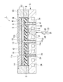
- FIG. 1 is a schematic cross-sectional view showing a preferred example of the electrostatic chuck device of the present embodiment.
- FIG. 2 is a schematic view showing an example of a composite sintered body according to the present invention.
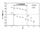
- FIG. 3 is a graph showing the relationship between slurry pH and zeta potential of particles in the slurry.
- FIG. 4 is a schematic explanatory drawing explaining the example of the preferable manufacturing method of the composite sintered compact of this invention.
- FIG. 5 is a schematic explanatory drawing explaining the example of the preferable manufacturing method of the composite sintered compact of this invention.
- FIG. 6 is a schematic explanatory view for explaining an example of a preferable production method of the composite sintered body of the present invention.
- FIG. 1 is a schematic cross-sectional view showing a preferred example of the electrostatic chuck device of the present embodiment.
- FIG. 2 is a schematic view showing an example of a composite sintered body according to the present invention.
- FIG. 3 is a graph showing the relationship
- FIG. 7 is a schematic explanatory drawing explaining the example of the preferable manufacturing method of the composite sintered compact of this invention.
- FIG. 8 is a schematic explanatory view for explaining an example of a preferable production method of the composite sintered body of the present invention.
- FIG. 9 is a schematic explanatory view for explaining an example of a preferable production method of the composite sintered body of the present invention.
- FIG. 6 is a BF-STEM photograph of the composite sintered body obtained in Example 1.
- FIG. It is the EDX measurement result of the composite sintered compact obtained in Example 1.
- FIG. It is the EDX measurement result of the composite sintered compact obtained in Example 1.
- FIG. 1 is a cross-sectional view showing the electrostatic chuck device of the present embodiment.
- the electrostatic chuck device 1 of the present embodiment has a disc-like electrostatic chuck portion 2 in plan view with one main surface (upper surface) side as a mounting surface, and is provided below the electrostatic chuck portion 2
- the temperature control base portion 3 in the form of a thick disk in plan view for adjusting the electric chuck portion 2 to a desired temperature is preferably provided.
- the electrostatic chuck 2 and the temperature control base 3 are bonded to each other through an adhesive layer 8 provided between the electrostatic chuck 2 and the temperature control base 3. The following will be described in order.
- the electrostatic chuck unit 2 has a mounting plate 11 whose upper surface is a mounting surface 11 a on which a plate-shaped sample W such as a semiconductor wafer is to be mounted, and the mounting plate 11 integrated with the mounting plate 11. And an insulating material layer 14 for insulating the periphery of the electrostatic adsorption electrode 13 and the electrostatic adsorption electrode 13 provided between the mounting plate 11 and the support plate 12. doing.
- the mounting plate 11 and the support plate 12 correspond to the “base” in the present invention.
- the mounting plate 11 and the support plate 12 be disk-shaped members having the same shape of the superposed surfaces.
- the mounting plate 11 and the support plate 12 are preferably made of a ceramic sintered body having mechanical strength and durability against a corrosive gas and its plasma. The forming materials of the mounting plate 11 and the support plate 12 will be described in detail later.
- a plurality of protrusions 11 b each having a diameter smaller than the thickness of the plate-like sample are formed on the placement surface 11 a of the placement plate 11 at predetermined intervals, and the protrusions 11 b support the plate-like sample W.
- the total thickness including the mounting plate 11, the support plate 12, the electrostatic adsorption electrode 13 and the insulating material layer 14, that is, the thickness of the electrostatic chuck portion 2 can be arbitrarily selected, for example, 0.7 mm as an example. More than and 5.0 mm or less.
- the thickness of the electrostatic chuck portion 2 when the thickness of the electrostatic chuck portion 2 is less than 0.7 mm, it may be difficult to secure the mechanical strength of the electrostatic chuck portion 2.
- the thickness of the electrostatic chuck portion 2 exceeds 5.0 mm, the heat capacity of the electrostatic chuck portion 2 increases, the thermal responsiveness of the plate-like sample W to be mounted is deteriorated, and the lateral direction of the electrostatic chuck portion The increase in heat transfer may make it difficult to maintain the in-plane temperature of the plate-like sample W in a desired temperature pattern.
- the thickness of each part demonstrated here is an example, Comprising: It does not restrict to the said range. You may change it arbitrarily according to conditions.
- the electrostatic chucking electrode 13 is used as an electrostatic chucking electrode for generating a charge and fixing the plate-like sample W with an electrostatic chucking force.
- the shape and size may be appropriately adjusted.
- the electrostatic chucking electrode 13 can be formed using an arbitrarily selected material.
- the electrode 13 for electrostatic adsorption is, for example, aluminum oxide-tantalum carbide (Al 2 O 3 -Ta 4 C 5 ) conductive composite sintered body, aluminum oxide-tungsten (Al 2 O 3 -W) conductive composite sintering Body, aluminum oxide-silicon carbide (Al 2 O 3 -SiC) conductive composite sintered body, aluminum nitride-tungsten (AlN-W) conductive composite sintered body, aluminum nitride-tantalum (AlN-Ta) conductive composite Conductive ceramics such as sintered body, yttrium oxide-molybdenum (Y 2 O 3 -Mo) conductive composite sintered body, or refractory metals such as tungsten (W), tantalum (Ta), molybdenum (Mo), etc. Preferably, it is formed.
- the thickness of the electrostatic chucking electrode 13 is not particularly limited, and can be arbitrarily selected.
- the thickness of the electrostatic attraction electrode 13 can be selected, for example, from 0.1 ⁇ m to 100 ⁇ m, more preferably from 1 ⁇ m to 50 ⁇ m, and still more preferably from 5 ⁇ m to 20 ⁇ m.
- the thickness of the electrostatic adsorption electrode 13 is less than 0.1 ⁇ m, it may be difficult to secure sufficient conductivity.
- the thickness of the electrostatic adsorption electrode 13 exceeds 100 ⁇ m, the electrostatic adsorption electrode 13 and the electrostatic adsorption electrode 13 are mounted due to the difference in the thermal expansion coefficient between the electrostatic adsorption electrode 13 and the mounting plate 11 and the support plate 12. Cracks may easily form in the bonding interface between the plate 11 and the support plate 12.
- the electrostatic attraction electrode 13 having such a thickness can be easily formed by a film forming method such as a sputtering method or a vapor deposition method, or a coating method such as a screen printing method.
- the insulating material layer 14 surrounds the electrostatic adsorption electrode 13 to protect the electrostatic adsorption electrode 13 from the corrosive gas and the plasma thereof, and at the boundary between the mounting plate 11 and the support plate 12, ie, electrostatic The outer peripheral area other than the adsorption electrode 13 is joined and integrated.
- the insulating material layer 14 is made of an insulating material of the same composition as that of the mounting plate 11 and the support plate 12 or of the same main component.
- the temperature control base portion 3 is for adjusting the electrostatic chuck portion 2 to a desired temperature, and is a thick disk-like member.
- this temperature control base portion 3 for example, a liquid cooled base or the like in which a flow path 3A for circulating a refrigerant is formed can be suitably used.
- the material constituting the temperature control base portion 3 is not particularly limited as long as it is a metal excellent in thermal conductivity, conductivity, and processability, or a composite material containing these metals.
- a metal excellent in thermal conductivity, conductivity, and processability or a composite material containing these metals.
- aluminum (Al), aluminum alloy, copper (Cu), copper alloy, stainless steel (SUS) and the like are suitably used.
- at least the surface of the temperature control base portion 3 exposed to plasma is subjected to an alumite treatment or an insulating film such as alumina is formed.
- An insulating plate 7 is bonded to the upper surface side of the temperature control base portion 3 via an adhesive layer 6.
- the adhesive layer 6 is formed of an arbitrarily selected material, and is preferably made of a sheet-like or film-like adhesive resin having heat resistance such as polyimide resin, silicon resin, or epoxy resin, and insulation.
- the thickness of the adhesive layer can be arbitrarily selected, and is formed, for example, to a thickness of about 5 to 100 ⁇ m.
- the insulating plate 7 is preferably made of a thin plate, sheet or film of heat resistant resin such as polyimide resin, epoxy resin or acrylic resin.
- the insulating plate 7 may be an insulating ceramic plate instead of the resin sheet, or may be a sprayed film having an insulating property such as alumina.
- the focus ring 10 is an annular member in a plan view, which is placed on the peripheral edge of the temperature control base 3.
- the focus ring 10 can be formed of an arbitrarily selected material, but for example, it is preferable to use a material having the same electrical conductivity as the wafer placed on the mounting surface.
- a feeding terminal 15 for applying a DC voltage to the electrostatic chucking electrode 13 is connected to the electrostatic chucking electrode 13.
- the power supply terminal 15 is inserted into the through hole 16 penetrating the temperature control base portion 3, the adhesive layer 8, and the support plate 12 in the thickness direction.
- An insulator 15 a having an insulating property is provided on the outer peripheral side of the power supply terminal 15.
- the power supply terminal 15 is insulated from the metal temperature control base portion 3 by the insulator 15a.
- FIG. 1 shows the power supply terminal 15 as an integral member
- a plurality of members may be electrically connected to constitute the power supply terminal 15.
- the power supply terminals 15 are inserted into the temperature control base 3 and the support plate 12 whose thermal expansion coefficients are different from each other. Therefore, for example, it is also preferable to configure the portions of the power supply terminal 15 inserted in the temperature control base portion 3 and the support plate 12 with different materials.
- the material of the part (extraction electrode) of the power supply terminal 15 connected to the electrostatic chucking electrode 13 and inserted into the support plate 12 is particularly limited as long as it is a conductive material having excellent heat resistance. It is not a thing.
- the material of the portion has a thermal expansion coefficient close to that of the electrostatic adsorption electrode 13 and the support plate 12.
- the portion of the power supply terminal 15 inserted into the temperature control base portion 3 is made of, for example, a metal material such as tungsten (W), tantalum (Ta), molybdenum (Mo), niobium (Nb), or Kovar alloy. It is preferable that
- These two members may be connected by a silicon-based conductive adhesive having flexibility and electrical resistance.
- a heater element 5 is provided on the lower surface side of the electrostatic chuck portion 2. Conditions such as the material and thickness of the heater element 5 can be arbitrarily selected.
- a nonmagnetic metal thin plate having a constant thickness of 0.2 mm or less, preferably about 0.1 mm, for example, a titanium (Ti) thin plate, a tungsten (W) thin plate, and molybdenum (Mo)
- Ti titanium
- W tungsten
- Mo molybdenum
- a preferable heater element can be obtained by processing a thin plate selected from thin plates or the like into a desired heater shape by, for example, photolithography or laser processing the entire outline of a shape in which a strip-like conductive thin plate is meandered.
- Such a heater element 5 may be provided by bonding a nonmagnetic metal thin plate to the electrostatic chuck portion 2 and then processing and molding the surface of the electrostatic chuck portion 2.
- the heater element 5 may be provided by transferring and printing on the surface of the electrostatic chuck portion 2 the one processed and formed as the heater element 5 at a position different from the electrostatic chuck portion 2.
- the heater element 5 is adhered and fixed to the bottom surface of the support plate 12 by an adhesive layer 4 made of a silicon resin or an acrylic resin in the form of a sheet or film having uniform heat resistance and insulation properties.
- the heater element 5 is connected to a power supply terminal 17 for supplying power to the heater element 5.
- a material which comprises the terminal 17 for electric power feeding the material equivalent to the material which comprises the terminal 15 for previous electric power feeding can be used.
- the power supply terminals 17 are provided so as to penetrate through holes 3 b formed in the temperature control base portion 3.
- a temperature sensor 20 is provided on the lower surface side of the heater element 5.
- the installation hole 21 is formed so as to penetrate the temperature control base portion 3 and the insulating plate 7 in the thickness direction, and the temperature sensor 20 is formed at the top of these installation holes 21. Is installed. It is desirable that the temperature sensor 20 be installed as close to the heater element 5 as possible. For this reason, the installation hole 21 may be extended and formed so as to protrude further to the adhesive layer 8 side from the structure shown in FIG. 1, and the temperature sensor 20 and the heater element 5 may be brought close to each other.
- the temperature sensor 20 can be selected arbitrarily, it is also preferable that it is a fluorescence type temperature sensor in which the fluorescent substance layer was formed in the upper surface side of the rectangular parallelepiped light transmission body which consists of quartz glass etc. as an example.
- the temperature sensor 20 configured as described above is bonded to the lower surface of the heater element 5 with a silicone resin based adhesive or the like having translucency and heat resistance.
- the phosphor layer is made of a material that emits fluorescence in response to the heat input from the heater element 5.
- a forming material of a fluorescent substance layer it should just be a material which emits fluorescence according to heat_generation
- the material for forming the phosphor layer is preferably a phosphor material to which a rare earth element having an energy rank suitable for light emission is added, a semiconductor material such as AlGaAs, a metal oxide such as magnesium oxide, ruby, sapphire or the like. A mineral can be mentioned and it can select suitably from these materials and can use it.
- the temperature sensor 20 corresponding to the heater element 5 is provided at an arbitrary position in the circumferential direction of the lower surface of the heater element 5 at a position not interfering with the power supply terminal or the like.
- the temperature measurement unit 22 includes an excitation unit 23 that irradiates the phosphor layer with excitation light to the outside (lower side) of the installation hole 21 of the temperature adjustment base unit 3, and the phosphor layer It comprises a fluorescence detector 24 for detecting emitted fluorescence, and a control unit 25 for controlling the excitation unit 23 and the fluorescence detector 24 and calculating the temperature of the main heater based on the fluorescence.
- the electrostatic chuck device 1 has a gas hole 28 provided so as to penetrate from the temperature control base portion 3 to the mounting plate 11 in the thickness direction thereof.
- a cylindrical insulator 29 is preferably provided on the inner peripheral portion of the gas hole 28.
- a gas supply device (cooling means) is connected to the gas hole 28. From the gas supply device, a cooling gas (heat transfer gas) for cooling the plate-like sample W is supplied through the gas holes 28. The cooling gas is supplied to the grooves 19 formed between the plurality of protrusions 11 b on the upper surface of the mounting plate 11 through the gas holes, thereby cooling the plate-shaped sample W.
- a cooling gas heat transfer gas
- the electrostatic chuck device 1 preferably has a pin insertion hole (not shown) provided so as to penetrate from the temperature control base portion 3 to the mounting plate 11 in the thickness direction thereof.
- the pin insertion hole can adopt, for example, the same configuration as that of the gas hole 28.
- a plate-like sample detachment lift pin is inserted into the pin insertion hole.
- the electrostatic chuck device 1 is configured as described above.
- FIG. 2 is a schematic view showing an example of a composite sintered body according to the present invention, which is a preferable forming material of a substrate.
- a composite sintered body according to the present invention which is a preferable forming material of a substrate.
- preferable examples of the composite sintered body according to the present invention, which can be preferably used for the substrate will be described.
- the composite sintered body 100 is formed of a ceramic composite sintered body containing aluminum oxide as a main phase and silicon carbide as a sub phase.
- the composite sintered body 100 has mullite in the aluminum oxide crystal grains.
- the main phase may be a region having an area ratio or volume ratio greater than 50% of the whole, and the sub phase may be considered as a region other than the main phase. It is also preferable that the main phase have an area ratio or a volume ratio that is 75% or more, or 80% or more. More specifically, for example, the main phase preferably has 85 to 96% by volume, and more preferably 87 to 95% by volume.
- the thermal conductivity is lower than that of a sintered body in which mullite does not exist.
- the influence of the heater of the electrostatic chuck device and the heat source such as plasma in the use environment is alleviated, and the uniformity of the entire substrate is improved.
- Mullite has lower durability when exposed to plasma as compared to silicon carbide and aluminum oxide. Therefore, when mullite exists in the grain boundary of aluminum oxide, when using the composite sintered body 100 in the plasma environment, mullite of the grain boundary is easily consumed. As a result, the physical properties of the composite sintered body in which mullite is present at grain boundaries are likely to change in a plasma environment. If the amount of mullite present in grain boundaries is large, the change in physical properties is also considered to be large.
- mullite exists in the crystal grains of aluminum oxide. There are no or very few mullite at grain boundaries. For this reason, even if it is used in a plasma environment, physical properties do not easily change, which is preferable.
- mullite is an aluminum silicate compound stable at high temperature.
- the chemical composition of mullite may range from 3Al 2 O 3 ⁇ 2SiO 2 -2Al 2 O 3 SiO 2.
- the Al / Si ratio of mullite can vary from three to four.
- the “mullite” in the present invention may be a compound represented by 3Al 2 O 3 .2SiO 2 or a compound represented by Al 6 O 13 Si 2 .
- the composite sintered body 100 shown in FIG. 2 includes a first crystal grain 110 which is a crystal grain of aluminum oxide, a second crystal grain 120 which is a crystal grain containing mullite, and a third crystal grain which is a crystal grain of silicon carbide. And 130.
- the third crystal grains 130 do not contain mullite.
- the plurality of second crystal grains 120 are dispersed in the crystal grains of the first crystal grain 110 in the main phase configured by sintering the plurality of first crystal grains 110. Further, the plurality of third crystal grains 130 exist in the grain boundaries 110 a of the first crystal grains 110.
- the composite sintered body 100 also has a fourth crystal grain 140 which is a crystal grain of silicon carbide.
- the fourth crystal grains are dispersed in the crystal grains of the first crystal grain 110.
- the fourth crystal grains 140 also contain no mullite.
- the third crystal grains 130 exist at grain boundaries, and the fourth crystal grains 140 are dispersed in the crystal grains of the first crystal grain.
- the average grain size of the fourth crystal grains can be selected arbitrarily, but is preferably 0.04 to 0.8 ⁇ m, more preferably 0.1 to 0.3 ⁇ m.
- the average grain size of the fourth crystal grains 140 is preferably smaller than the average grain size of the third crystal grains 130.
- the second crystal grains 120 containing mullite can be confirmed, for example, by elemental analysis of an arbitrary cross section of the composite sintered body 100 by energy dispersive X-ray analysis (EDX). It can be judged that silicon carbide and aluminum oxide react with each other in "a portion in which a silicon atom is not detected" in "a portion in which a silicon atom is detected” in EDX, and mullite is generated. A crystal grain including a portion where such mullite is generated is specified as a second crystal grain 120.
- EDX energy dispersive X-ray analysis
- the average crystal grain size of the first crystal grain 110 may be arbitrarily selected, but is preferably 0.5 ⁇ m or more and 10 ⁇ m or less, and more preferably 0.8 ⁇ m or more and 1.6 ⁇ m or less.
- the average crystal grain size of the first crystal grains 110 is 0.5 ⁇ m or more, the decrease in the thermal conductivity can be suppressed without the number of grain boundaries being too large. Therefore, when the composite sintered body 100 is heated or cooled, it is easy to follow the temperature change.
- the average grain size of the first crystal grain is taken an electron micrograph, and the major axis diameter of the crystal grain of 200 or more first crystal grains is calculated, and this arithmetic average value is calculated as the average grain size. It can be diameter.
- the composite sintered body 100 can easily maintain the heat uniformity.
- the second crystal grains 120 contain mullite that is produced by the reaction of silicon carbide, which is a raw material of the composite sintered body 100, and aluminum oxide.
- the second crystal grain 120 may partially contain mullite and the remaining part may be silicon carbide, or may be composed only of mullite.
- the proportion of mullite in the second crystal grains can be set as needed.
- the average grain size of the second crystal grains 120 is preferably smaller than the average grain size of the third crystal grains 130.
- the average grain size of the second crystal grains 120 can be selected arbitrarily.
- the average crystal grain size of the second crystal grains 120 is preferably 0.03 ⁇ m or more and 0.2 ⁇ m or less.
- the second crystal grains 120 can sufficiently influence the thermal conductivity of the composite sintered body 100.
- the average grain size of the second crystal grains 120 is 0.2 ⁇ m or less, mullite is suitably formed.
- the average crystal grain size of the third crystal grains 130 can be arbitrarily selected, but is preferably 0.9 ⁇ m or less. When the average crystal grain size of the third crystal grain 130 is 0.9 ⁇ m or less, the electric field applied to the composite sintered body 100 is less likely to be attenuated inside the third crystal grain, and the loss coefficient is less likely to be deteriorated.
- the lower limit of the average grain size of the third crystal grains 130 can be selected arbitrarily.
- the second crystal grain 120 is preferably smaller than the third crystal grain 130 of the grain boundary. As the second crystal grain 120 is smaller, mullite is easily formed and desired physical properties are easily obtained. By mullite, it is meant that crystals containing mullite are formed.
- the ratio of the entire second crystal grain 120 to the whole of the third crystal grain 130 can be arbitrarily selected, but it is 20% or more and 40% or less in area ratio preferable. It may be 25% or more in area ratio. It may be 35% or less in area ratio.
- the mullite content rate is set to a desired value described later Becomes easier. In addition, it is easy to obtain desired physical properties.
- the ratio of the entire second crystal grains 120” in the composite sintered body 100 is calculated from a scanning electron micrograph of an arbitrarily selected field of view of the composite sintered body.
- an electron micrograph is taken at a magnification of 10000 times in a randomly selected field of view, and silicon carbide grains (third crystal grains 130) present in the grain boundaries shown in the electron micrograph.
- the total area is taken as the area of “the entire third crystal grain 130”.
- the “second crystal grains 120” are specified by the above-described method, and the area of “the entire“ second crystal grains 120 ”is determined. From the area thus determined, the ratio of “the entire second crystal grain 120” to “the whole third crystal grain 130” is determined as the area ratio.
- crystal grains containing mullite similar to the second crystal grains 120 may be present in the grain boundaries 110a. However, it is preferable that mullite does not exist in the grain boundaries 110a. In addition, the crystal grain which contains a mullite which exists in the crystal grain boundary 110a is not judged as the 2nd crystal grain 120.
- FIG. The area ratio of the second crystal grain 120 to the crystal grain containing mullite in the grain boundary 110a can be selected arbitrarily.
- the area ratio between the second crystal grain 120 and the mullite-containing crystal grain in the grain boundary 110a may be, for example, an area ratio of 100 to 90: 0 to 10, etc., and 100 to 95: 0 to 5
- the area ratio may be, for example, 100 to 99: 0 to 1.
- the average crystal grain size of the crystal grains of silicon carbide contained in the composite sintered body 100 that is, the crystal of silicon carbide obtained by combining the third crystal grain 130 and the fourth crystal grain 140
- the average grain size of the grains can be selected arbitrarily, but is preferably 0.2 ⁇ m or more and 0.8 ⁇ m or less.
- crystal grains of silicon carbide having a large crystal grain size easily follow the movement of the grain boundaries of alumina at the time of growth of alumina grains, and the position of the grains easily changes according to the growth of alumina crystal grains. Therefore, crystal grains of silicon carbide having a large crystal grain size are excluded without being taken into the inside of the growing alumina, and easily located at crystal grain boundaries of the sintered body.
- silicon carbide having an average crystal grain size as small as 0.2 ⁇ m or more and 0.8 ⁇ m or less does not easily follow the grain boundary movement of alumina at the time of alumina particle growth. Therefore, crystal grains of silicon carbide having a small crystal grain size are easily taken into the inside of the grain-growing alumina.
- silicon carbide present in alumina grains tends to have a smaller grain size than silicon carbide present in grain boundaries.
- the area ratio between the third crystal grain 130 and the fourth crystal grain 140 can be arbitrarily selected.
- the content of mullite with respect to the composite sintered body 100 can be arbitrarily selected, but is 1.2% or more and 3.5% or less in area ratio in the cross section selected arbitrarily Is preferred.
- the content rate of mullite is 1.2% or more in area ratio, sufficient thermal conductivity can be secured.
- the area ratio may be 1.5% or more, 2.0% or more, or 2.5% or more.
- the area ratio may be 3.0% or less, 2.5% or less, or 2.0% or less.
- the composite sintered body 100 which is a forming material of the mounting plate 11 and the support plate 12, has a high heat uniformity because of the configuration as described above.
- Silicon carbide is known to have a large number of crystal structures, and has a cubic system having a 3C-type (zinc blende-type) crystal structure, a 4H-type, a 6H-type or other hexagonal crystal.
- 3C-type zinc blende-type
- 4H-type a 4H-type
- 6H-type or other hexagonal crystal those having a wurtzite crystal structure, and those having a rhombohedral system and a 15R crystal structure can be mentioned.
- ⁇ -SiC one having a 3C type crystal structure
- all materials having a crystal structure other than that are referred to as “ ⁇ -SiC”.
- ⁇ -SiC can be particularly preferably contained in the composite sintered body.
- SiC contained in the composite sintered body is ⁇ -SiC. Further, in the sintered body, it is preferable that crystal grains of ⁇ -SiC are dispersed and present in a state of being surrounded by crystal grains of a metal oxide which is a matrix material. In the sintered body, the volume ratio of ⁇ -SiC can be arbitrarily selected.
- the amount of SiC, preferably ⁇ -SiC, is preferably 4% by volume or more and 15% by volume or less of the whole sintered body, and more preferably 5% by volume or more and 13% by volume or less.
- volume ratio of SiC preferably ⁇ -SiC
- the effect of expressing electronic conductivity by SiC particles may be small.
- volume ratio of ⁇ -SiC is more than 15% by volume, contact between SiC particles may occur to cause a decrease in resistance value through the SiC particles.
- the content of metal impurities other than aluminum and silicon is preferably 100 ppm or less.
- the metal impurity content is preferably 50 ppm or less, more preferably 25 ppm or less.
- the composite sintered body according to the present embodiment can be preferably produced by mixing aluminum oxide particles and silicon carbide particles and sintering them. At that time, with regard to silicon carbide particles that are taken into a plurality of aluminum oxide particles and sintered, (i) increase the amount of silicon carbide particles described below, (ii) reduce the particle diameter of silicon carbide particles,
- the above-described composite sintered body can be preferably manufactured by control.
- the composite sintered body of the present invention can be obtained by the present manufacturing method.
- the composite sintered body of the present invention and the composite sintered body according to the present embodiment can be suitably manufactured by the following method.
- the manufacturing method of the composite sintered body of the present embodiment is (A) injecting aluminum oxide particles and silicon carbide particles at high speed and mixing them while causing them to collide with each other; (B) adjusting the pH of the slurry to such a range that the surface charge of the aluminum oxide particles in the slurry becomes positive and the surface charge of the silicon carbide particles in the slurry becomes negative for the slurry obtained in the mixing step When, (C) forming a pH after adjusting the pH and removing the dispersion medium from the slurry; And (d) pressure-sintering the obtained molded body by heating to 1600 ° C. or higher while pressing and compacting in a non-oxidative atmosphere at a pressure of 25 MPa or higher.
- the content of aluminum oxide in the aluminum oxide particles to be used is preferably 99.99% or more.
- Such high purity aluminum oxide particles can be prepared by using the alum method.
- the aluminum oxide particles prepared using the alum method can significantly reduce the content of sodium atoms, which are metal impurities, as compared to aluminum oxide particles prepared using, for example, the Bayer method.
- various methods can be employed as long as aluminum oxide particles of desired purity can be obtained.
- (A) Process of mixing In the mixing step, aluminum oxide particles and silicon carbide particles (dispersion liquid) dispersed in a dispersion medium are prepared. It is preferable that the two-particle collision type pulverizing and mixing apparatus be used to inject the particles at high speed by pressurizing each of the dispersion liquids to mix the particles while causing the particles to collide with each other. Thereby, the aluminum oxide particles and the silicon carbide particles are crushed, and a dispersion containing these crushed particles is obtained. In this process, it is only necessary for the slurries separately jetted at high speed to collide with each other. The speed at which the slurry collides may be arbitrarily selected.
- the aluminum oxide particles and the silicon carbide particles obtained by using the above-mentioned pulverizing and mixing apparatus become particles having a small particle size distribution width and a small number of coarse particles and excessively pulverized particles. Therefore, when the mixed particles pulverized and mixed using the two-stream particle collision type pulverizing and mixing apparatus are used, abnormal particle growth can be suppressed in the sintering step with coarse particles as nuclei.
- the silicon carbide particles to be used may be subjected to a heat treatment in an oxidizing atmosphere to oxidize the surface of the silicon carbide particles in advance.
- pre-oxidation the above oxidation treatment is referred to as "pre-oxidation”.
- the temperature conditions of pre-oxidation can be selected arbitrarily, for example, 300 degreeC or more and 500 degrees C or less are preferable.
- the pre-oxidation temperature is 300 ° C. or more
- the surface of the silicon carbide particles can be oxidized.
- the pre-oxidation temperature is 500 ° C. or less
- oxidation of the surface of the silicon carbide particles does not proceed too much.
- the oxidation temperature is set to 600 ° C. or more, oxidation of the surface of the silicon carbide particles proceeds too much, and as a result, silicon carbide particles may be bonded via the oxide film on the particle surfaces and coarsened.
- the time of pre-oxidation can be selected arbitrarily, 10 hours or more are preferable. If the pre-oxidation time is less than 10 hours, the oxidation does not proceed sufficiently.
- the pre-oxidation time may be a long time (for example, 50 hours), but after a certain amount of oxide film is formed, the amount of oxide film hardly changes. Therefore, the pre-oxidation time is preferably, for example, 10 hours or more and 20 hours or less.
- the hydrophilicity of the silicon carbide particles is enhanced. This improves the dispersibility of the silicon carbide particles in the slurry.
- the kind of dispersion medium can be selected arbitrarily, distilled water etc. can be preferably used if an example is given.
- the ratio of aluminum oxide particles to silicon carbide particles to be used for mixing can be arbitrarily selected, but the volume ratio is preferably 85 to 96/4 to 15, and more preferably 87 to 95/5 to 13.
- the particle diameter of the aluminum oxide particles dispersed in the dispersion medium can be arbitrarily selected, but it is preferably 0.1 to 0.3 ⁇ m, and more preferably 0.15 to 0.25 ⁇ m.
- the particle diameter of the silicon carbide particles in the dispersion medium before the injection can be arbitrarily selected, but it is preferably 10 to 150 nm, and more preferably 30 to 100 nm.
- the proportion of the aluminum oxide particles in the particles in the dispersion medium before the injection can be arbitrarily selected, but preferably 85 to 96% by volume, and more preferably 87 to 95% by volume, as an example.
- the proportion of silicon carbide particles in the particles in the dispersion medium before the injection can be arbitrarily selected, but it is preferably 4 to 15% by volume, and more preferably 5 to 13% by volume, as an example.
- the ratio of the total amount of the silicon carbide particles and the aluminum oxide particles to the amount of the dispersion medium in the dispersion medium before the injection can be arbitrarily selected. If an example is given, 10 mass% or more, 20 mass% or more, 30 mass% or more, 40 mass% or more can be mentioned as an example of a lower limit. As an example of an upper limit, 90 mass% or less, 80 mass% or less, 70 mass% or less etc. can be mentioned preferably.
- the method of preparing the aluminum oxide particles and the silicon carbide particles dispersed in the dispersion medium to be used for the grinding and mixing can be arbitrarily selected. For example, aluminum oxide particles and silicon carbide particles may be added continuously or simultaneously to the dispersion medium.
- aluminum oxide particles may be dispersed in a dispersion medium
- silicon carbide particles may be dispersed in the same separately prepared dispersion medium.
- These two dispersions may be mixed and used, or may be jetted separately.
- the dispersant may be added in advance to any amount of dispersion medium, and this may be used. The dispersant can be selected arbitrarily.
- (B) Step of adjusting pH The pH of the obtained mixed solution (slurry) is adjusted. In this step, pH adjustment is performed in consideration of the surface charge of the aluminum oxide particles and the silicon carbide particles contained in the slurry.
- the slurry (slurry before pH adjustment) obtained in the mixing step usually exhibits basicity of about pH 11.
- FIG. 3 is a graph showing the relationship between slurry pH and zeta potential of particles for aluminum oxide particles and silicon carbide particles in a slurry.
- the horizontal axis indicates the pH of the slurry
- the vertical axis indicates the zeta potential (unit: mV) of each particle.
- the solvent of the slurry before pH adjustment is 0.1 N NH 4 NO 3.
- the aluminum oxide particles have positive zeta potential. This is because when the pH of the system is on the acidic side, the hydroxyl groups on the surface of the aluminum oxide particles are protonated (H + ) and the surface is positively charged.
- the aluminum oxide particles have a negative zeta potential. This is because when the pH of the system is on the basic side, protons are dissociated from the hydroxyl groups on the surface of the aluminum oxide particles, and the surface is negatively charged.
- the behavior of the zeta potential of the silicon carbide particles is different.
- the silicon carbide particles have a zeta potential of 0 around pH 2 to 3, and a negative zeta potential in a wide range from an acidic region around pH 3 to a basic region.
- the pH of the system is "the surface charge of the aluminum oxide particles in the slurry is positive" and the “the surface charge of the silicon carbide particles in the slurry is negative" In the range of ",” so-called heteroflocculation occurs in which both particles clump.
- a dispersant be appropriately added to the slurry so that aluminum oxide particles and silicon carbide particles do not precipitate.
- the pH of the system is preferably 3 or more and 7 or less, more preferably 5 or more and 7 or less, and still more preferably 6 or more and 7 or less.
- Adjustment of pH to the above-mentioned range can be performed by adding an acid to a slurry.
- usable acids include inorganic acids such as nitric acid, phosphoric acid, hydrochloric acid and sulfuric acid, and organic acids such as acetic acid.
- inorganic acids such as nitric acid, phosphoric acid, hydrochloric acid and sulfuric acid
- organic acids such as acetic acid.
- hydrochloric acid, sulfuric acid or the like may generate chlorine or sulfur in the apparatus in the sintering step described later, which may cause the apparatus to be deteriorated. Therefore, it is preferable to use nitric acid, phosphoric acid, an organic acid or the like for adjusting the pH.
- the obtained granules are molded, for example, uniaxially molded (uniaxial press molded).
- the resulting shaped body is then heated under an inert gas atmosphere at normal pressure (without pressing) at a temperature optionally selected.
- a temperature optionally selected.
- the mixture is heated to 500 ° C. to remove contaminants such as moisture and dispersion medium contained in the molded body.
- Nitrogen or argon can be used as the inert gas.
- the heating temperature is not limited to 500 ° C. as long as contaminants can be removed from the compact without denaturing the compact. For example, 350 to 600 ° C., and more preferably 450 to 550 ° C. may be mentioned as an example.
- the oxidation process of oxidizing the mixed particles that form the compact by heating the compact from which contaminants have been removed in the air at a temperature selected according to need, for example 400 ° C. preferable.
- a temperature selected according to need for example 400 ° C. preferable.
- an oxide film is formed on the surface of silicon carbide particles contained in the mixed particles in the oxidation treatment.
- metal impurities contained in the mixed particles are easily dissolved out. For this reason, metal impurities contained in the mixed particles are biased to the surface of the particles. Then, it is preferable because metal impurities are easily removed in a pressure sintering process described later.
- the temperature of the oxidation treatment is not limited to 400 ° C., and may be, for example, 250 to 500 ° C., more preferably 300 to 450 ° C., as needed.
- the time of the oxidation treatment can be arbitrarily selected, and is, for example, 6 to 48 hours, and more preferably 12 to 24 hours.
- (D) Step of pressure sintering In the pressure-baking step, first, the above-mentioned molded body obtained in the above-described step is subjected to (without pressing) at a temperature lower than 1600 ° C. and normal pressure in a vacuum atmosphere (first non-oxidizing atmosphere) ), Heating (preheating). According to such an operation, by appropriately setting the temperature at the time of the preheating, metal impurities such as alkali metals contained in the mixed particles are evaporated, and the metal impurities can be easily removed. Therefore, according to such an operation, the purity of the mixed particles can be easily improved, and the volume resistance value of the substrate can be easily controlled.
- the temperature lower than 1600 ° C. can be selected as required.
- the oxide film formed on the particle surface is volatilized by preheating in a vacuum atmosphere in this step.
- metal impurities contained in the oxide film evaporate. Therefore, metal impurities can be easily removed from the molded body. Therefore, according to such an operation, the purity of the mixed particles can be easily improved, and the volume resistance value of the substrate can be easily controlled.
- vacuum refers to “a state in a space filled with a substrate having a pressure lower than atmospheric pressure”, which is a state defined as a pressure that can be industrially used according to the JIS standard. Point to In the present embodiment, the vacuum atmosphere may be low vacuum (100 Pa or more), but is preferably medium vacuum (0.1 Pa to 100 Pa), and high vacuum (10 -5 Pa to 0.1 Pa) Is more preferable.
- the pressure is preferably returned to atmospheric pressure with an inert gas such as argon.
- the compact which has been subjected to the preheating is heated to 1600 ° C. or higher while being compressed at a pressure of 5 MPa or more in an inert gas atmosphere, for example, an argon atmosphere (second non-oxidizing atmosphere).
- an inert gas atmosphere for example, an argon atmosphere (second non-oxidizing atmosphere).
- sintering can be performed at a sintering pressure of 25 MPa or more and 50 MPa or less at a temperature of 1600 ° C. or more and 1850 ° C. or less under an argon atmosphere.
- the sintered body produced by such a method has a reduced metal impurity content and becomes a highly pure sintered body. If the metal impurity content does not reach the target value, the preheating time may be increased or the preheating temperature may be increased.
- FIG. 4 to 9 are explanatory views for explaining the method of manufacturing the composite sintered body according to the present embodiment.
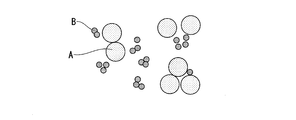
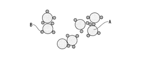
- 4 to 6 show the state of the particles at each stage when the pH of the slurry is adjusted to about pH 11, and FIGS. 7 to 9 show the particles at each stage when the pH of the slurry is adjusted to about pH 6.5.
- the state is schematically shown. These figures are described below. First, steps without pH adjustment will be described.
- FIG. 4 is a schematic view showing the state of particles in a slurry of about pH 11, for example.
- FIG. 5 is a schematic view showing the state of particles when the dispersion medium is removed from the slurry shown in FIG.
- FIG. 6 is a schematic view showing a composite sintered body produced using the particles shown in FIG.
- the hexagons in the respective drawings indicate crystal grains of aluminum oxide which is the main phase.
- black circles in each figure indicate crystal grains of silicon carbide which is the sub phase, and the size of the black circles indicates the size of crystal grains of silicon carbide.
- symbol A indicates aluminum oxide particles
- symbol B indicates silicon carbide particles.
- both of the aluminum oxide particles and the silicon carbide particles have a negatively charged surface (the zeta potential is negative). Repel each other.
- FIG. 7 is a schematic view showing, for example, a state after adjusting the slurry of FIG. 4 from pH 11 to about pH 6.5. 7 to 9 correspond to FIGS. 4 to 6, respectively.
- the dispersibility of silicon carbide particles improves. Therefore, when using the silicon carbide particle which performed the pre-oxidation process, the homo aggregation of silicon carbide particle can be suppressed and the said hetero aggregation can be advanced favorably. This makes it easier to obtain the desired aggregation state.
- the heterogeneous particles are easily mixed uniformly due to the aggregation of the aluminum oxide to which silicon carbide has already adhered to the surface. to be born.
- the step of (d) sintering the aluminum oxide particles are easily sintered together while incorporating silicon carbide particles.
- silicon carbide of relatively small crystal grains is difficult to follow this movement even if aluminum oxide particles move. Therefore, silicon carbide of small crystal grains is easily taken into the grain boundary of aluminum oxide as small crystal grains.
- the second crystal grains present in the crystal grains tend to be smaller than the third crystal grains 130 present in the grain boundaries.
- the composite sintered body of the present embodiment can be manufactured.
- the resulting composite sintered body can be ground in a subsequent step to form a desired substrate.
- the protrusions formed on the mounting surface of the base can be appropriately formed by a known method.
- the composite sintered body as described above is excellent in heat uniformity.
- the electrostatic chuck unit and electrostatic chuck device using such a composite sintered body it is excellent in heat uniformity and high performance that can realize high processing accuracy when applied to a processing apparatus. It becomes.
- the surface of the composite oxide (sintered body) was mirror-polished with a 3 ⁇ m diamond paste, and then thermal etching was performed at 1400 ° C. for 30 minutes in an argon atmosphere.
- the surface of the obtained sintered body was subjected to structure observation at a magnification of 10000 using a scanning electron microscope (manufactured by Hitachi High-Technologies Corporation, model number: S-4000).
- the obtained electron micrograph was incorporated into image analysis type particle size distribution measurement software (Mac-View Version 4) to calculate the area of 200 or more silicon carbide particles in grain boundaries or in the grains. From the electron micrographs, it was determined whether or not each silicon carbide particle was present in the metal oxide crystal grains. In addition, silicon carbide as the second crystal grain dispersed in the metal oxide crystal grain with respect to the whole silicon carbide particle as the third crystal grain whose area is determined using the result of the FFT analysis of the STEM image. The proportion of crystal grains was determined.
- the electron micrograph was incorporated into image analysis type particle size distribution measurement software (Mac-View Version 4), and the major axis diameter of the crystal grains of 200 or more first crystal grains was calculated. The arithmetic mean value of the major axis diameter of each of the obtained crystal grains was taken as the "average grain size" to be determined.
- the thermal conductivity was calculated from the measurement result of the thermal diffusivity by the laser flash method and the measurement result of the specific heat by the DSC method.
- a sintered body having a diameter of 350 mm ⁇ 1 mm was prepared and used as a test body. Specifically, a sintered body having a diameter of 350 mm and a thickness greater than 1 mm was produced, and then the surface was subjected to surface grinding to adjust the thickness to obtain a sintered body (test body) having a thickness of 1 mm.
- the obtained test body for temperature uniformity evaluation was sandwiched between a first metal plate with a diameter of 350 mm having a heater and a second metal plate with a diameter of 350 mm.
- the test body was heated using a heating plate, and the temperature of the test body was given a temperature gradient so that the heating plate side is high and the cooling plate side is low. Five minutes after the start of heating, the heat flow of the test plate was considered to be in a steady state, and the temperatures of three surfaces of the test body on the cooling plate side were measured.
- the measurement position is the center of the test body (coordinate position 0, 0), -160 mm in the 270 ° direction from the center of the test body (coordinate position -160, 0), 160 mm in the 90 ° direction from the center (160, 0 ).
- the temperature uniformity was evaluated as good. Also, when the difference between the maximum value and the minimum value of the measurement temperature exceeds 5 ° C., it was evaluated that the thermal uniformity is defective.
- Example 1 Starting materials are ⁇ -SiC type silicon carbide ( ⁇ -SiC) particles having an average particle size of 0.03 ⁇ m and synthesized by thermal plasma CVD, and an average particle size of 0.1 ⁇ m and a metal impurity content of 95 ppm And aluminum oxide (Al 2 O 3 ) particles were used.
- ⁇ -SiC ⁇ -SiC type silicon carbide
- pre-oxidation The ⁇ -SiC particles were heat-treated at 500 ° C. for 12 hours in the air atmosphere to oxidize the particle surfaces.
- pre-oxidation the above oxidation treatment is referred to as "pre-oxidation”.
- pre-oxidized ⁇ -SiC was used.
- the total amount of ⁇ -SiC particles and Al 2 O 3 particles was weighed so that the amount of ⁇ -SiC particles was 8.5% by mass, and was added to distilled water containing a dispersant. Further, the ratio of the total of ⁇ -SiC particles and Al 2 O 3 particles to distilled water was 60 mass%.
- the dispersion in which ⁇ -SiC particles and Al 2 O 3 particles were charged was subjected to dispersion treatment with an ultrasonic dispersion device, and then pulverized and mixed using a two-stream particle collision type grinding and mixing device.
- nitric acid was added to the slurry to adjust the pH of the slurry to 6.5.
- the slurry whose pH was adjusted was spray-dried by a spray-dryer to obtain dried mixed particles of ⁇ -SiC and Al 2 O 3 .
- the mixed particles were uniaxially press molded at a press pressure of 8 MPa to form a compact having a diameter of 320 mm ⁇ 15 mm.
- the obtained molded body was set in a mold made of graphite, and was heated to 370 ° C. without applying a pressing pressure to remove water and dispersant (contaminants). After that, the compact from which the contaminants were removed was heated to 370 ° C. in the air to oxidize the surface of the ⁇ -SiC particles contained in the compact.
- Example 1 Thereafter, sintering was performed at a pressure of 40 MPa and 1800 ° C. in an argon atmosphere to obtain a composite sintered body of Example 1.
- the electron micrograph was image
- the obtained electron micrograph to obtain an average crystal particle size of the Al 2 O 3 crystal grains (first crystal grains 110) was 0.94 .mu.m.
- FIG. 10 to 12 are EDX mappings showing EDX measurement results of the composite sintered body of Example 1.
- FIG. FIG. 10 is a BF-STEM photograph of the composite sintered body.
- FIG. 11 is an EDX measurement result which shows the location of carbon brightly in the same view as FIG.
- FIG. 12 is an EDX measurement result which shows the presence location of silicon brightly in the same view as FIG.
- FIGS. 10 to 12 it can be seen that there is a difference in the locations where silicon atoms and carbon atoms exist. It can be judged that mullite is formed in the place where a silicon atom exists but a carbon atom does not exist.
- FFT Fast Fourier Transform
- the average crystal grain size of the crystal grain (the second crystal grain 120) containing mullite was determined to be 0.07 ⁇ m. Further, the average crystal grain size of the crystal grains of SiC (the third crystal grain 130) was determined to be 0.37 ⁇ m. The second crystal grains 120 were smaller than the third crystal grains 130.
- the thermal conductivity of the obtained composite sintered body was 21.1 W / m ⁇ K.
- Example 2 The composite sintered body of Example 2 was obtained in the same manner as Example 1, except that the amount of ⁇ -SiC particles was 4 mass% with respect to the total amount of ⁇ -SiC particles and Al 2 O 3 particles. .
- the electron micrograph was image
- the obtained electron micrograph to obtain an average crystal particle size of the Al 2 O 3 crystal grains (first crystal grains 110) was 1.05 .mu.m.
- the average crystal grain size of the crystal grains of SiC was determined to be 0.35 ⁇ m.
- the second crystal grains 120 were smaller than the third crystal grains 130.
- the thermal conductivity of the obtained composite sintered body was 24.0 W / m ⁇ K.
- Starting materials are ⁇ -SiC type ⁇ -SiC particles having an average particle size of 0.03 ⁇ m and synthesized by thermal plasma CVD, and Al 2 O having an average particle size of 0.1 ⁇ m and a metal impurity content of 95 ppm. Three particles were used.
- the total amount of ⁇ -SiC particles and Al 2 O 3 particles was weighed so that the amount of ⁇ -SiC particles was 8.5% by mass, and was added to distilled water containing a dispersant.
- the dispersion in which ⁇ -SiC particles and Al 2 O 3 particles were charged was subjected to dispersion treatment with an ultrasonic dispersion device, and then pulverized and mixed using a two-stream particle collision type grinding and mixing device.
- the obtained mixed solution was spray-dried with a spray dryer without pH adjustment to obtain mixed particles of ⁇ -SiC and Al 2 O 3 .
- Example 2 molding was performed in the same manner as in Example 1, and the molded body was heated to 500 ° C. in a nitrogen atmosphere without applying a pressing pressure to remove water and dispersant (contaminants). Thereafter, the compact from which the impurities were removed was heated to 400 ° C. in the air to oxidize the surface of the ⁇ -SiC particles contained in the compact.
- the obtained compact was set in a graphite mold and subjected to pressure sintering.
- the molded body was heated to 1200 ° C. in a vacuum atmosphere without applying a pressing pressure.
- sintering was performed at a pressure of 40 MPa and 1800 ° C. in an argon atmosphere to obtain a sintered body of Comparative Example 1.
- the electron micrograph was image
- the obtained electron micrograph to obtain an average crystal particle size of the Al 2 O 3 crystal grains (first crystal grains 110) was 0.78 .mu.m.
- mullite could not be confirmed in the crystal grains of the first crystal grain 110.
- the average crystal grain size of the crystal grains of SiC was determined to be 0.31 ⁇ m.
- the thermal conductivity of the obtained composite sintered body was 28.8 W / m ⁇ K.
- Table 1 is a table in which the compositions and crystal grains of the sintered bodies of Examples 1 and 2 and Comparative Example 1 are summarized.
- Table 2 is the table
- the composite sintered body of the example had a thermal conductivity lower than that of the composite sintered body of the comparative example.
- the composite sintered body of the example exhibited better temperature uniformity than the composite sintered body of the comparative example.
- a novel composite sintered body having high thermal uniformity.
- an electrostatic chuck unit and an electrostatic chuck device using such a composite sintered body are provided.
Landscapes
- Chemical & Material Sciences (AREA)
- Engineering & Computer Science (AREA)
- Ceramic Engineering (AREA)
- Manufacturing & Machinery (AREA)
- Materials Engineering (AREA)
- Structural Engineering (AREA)
- Organic Chemistry (AREA)
- Inorganic Chemistry (AREA)
- Composite Materials (AREA)
- Thermal Sciences (AREA)
- Physics & Mathematics (AREA)
- Container, Conveyance, Adherence, Positioning, Of Wafer (AREA)
- Compositions Of Oxide Ceramics (AREA)
Abstract
Description
本願は、2017年6月29日に、日本に出願された特願2017-127095号に基づき優先権を主張し、その内容をここに援用する。
上記で述べた特徴は、互いに組み合わせることも好ましい。組み合わせは任意に選択してよく、任意に選択される2つの特徴を組み合わせてもよく、3つ以上の特徴を組み合わせても良い。
図1は、本実施形態の静電チャック装置を示す断面図である。本実施形態の静電チャック装置1は、一主面(上面)側を載置面とした平面視円板状の静電チャック部2と、この静電チャック部2の下方に設けられて静電チャック部2を所望の温度に調整する、厚みのある平面視円板状の温度調節用ベース部3と、を好ましく備えている。また、静電チャック部2と温度調節用ベース部3とは、静電チャック部2と温度調節用ベース部3の間に設けられた接着剤層8を介して接着されている。
以下、順に説明する。
静電チャック部2は、上面を半導体ウエハ等の板状試料Wを載置する載置面11aとした載置板11と、この載置板11と一体化され該載置板11の底部側を支持する支持板12と、これら載置板11と支持板12との間に設けられた静電吸着用電極13および静電吸着用電極13の周囲を絶縁する絶縁材層14と、を有している。載置板11および支持板12は、本発明における「基体」に該当する。
温度調節用ベース部3は、静電チャック部2を所望の温度に調整するためのもので、厚みのある円板状の部材である。この温度調節用ベース部3としては、例えば、その内部に冷媒を循環させる流路3Aが形成された液冷ベース等が好適に使用できる。
フォーカスリング10は、温度調節用ベース部3の周縁部に載置される、平面視で円環状の部材である。フォーカスリング10は、任意に選択される材料で形成できるが、例えば、載置面に載置されるウエハと同等の電気伝導性を有する材料を形成材料とすることが好ましい。このようなフォーカスリング10を配置することにより、ウエハの周縁部においては、プラズマに対する電気的な環境をウエハと略一致させることができ、ウエハの中央部と周縁部とでプラズマ処理の差や偏りを生じにくくすることができる。
静電吸着用電極13には、静電吸着用電極13に直流電圧を印加するための、給電用端子15が接続されている。給電用端子15は、温度調節用ベース部3、接着剤層8、及び、支持板12を厚み方向に貫通する貫通孔16の内部に挿入されている。給電用端子15の外周側には、絶縁性を有する碍子15aが設けられている。この碍子15aにより、金属製の温度調節用ベース部3に対して給電用端子15が絶縁されている。
静電チャック装置1は、以上のような構成となっている。
次に、本実施形態の基体(載置板11および支持板12)について詳述する。図2は、基体の好ましい形成材料である、本発明に係る複合焼結体の例を示す模式図である。
以下に、前記基体に好ましく使用できる、本発明に係る複合焼結体の好ましい例について説明する。
第2結晶粒120と、結晶粒界110aにあるムライトを含む結晶粒との面積比は、任意に選択できる。第2結晶粒120と、結晶粒界110aにあるムライトを含む結晶粒との面積比は、例えば、100~90:0~10などの面積比であっても良く、100~95:0~5などの面積比であってもよく、100~99:0~1などの面積比であっても良い。
なお第3結晶粒130と第4結晶粒140との面積比は、任意に選択できる。
本実施形態に係る複合焼結体は、酸化アルミニウム粒子と炭化ケイ素粒子とを混合し、焼結させることにより好ましく製造できる。その際、複数の酸化アルミニウム粒子に取り込まれて焼結する炭化ケイ素粒子については、以下に述べる(i)炭化ケイ素粒子の量を多くする、(ii)炭化ケイ素粒子の粒子径を小さくする、という制御により、上述した複合焼結体を好ましく製造することができる。本製造方法により、本発明の複合焼結体を得ることができる。
本実施形態の複合焼結体の製造方法は、
(a)酸化アルミニウム粒子と炭化ケイ素粒子とを、それぞれ高速で噴射してお互いに衝突させながら混合する工程と、
(b)混合する工程で得られたスラリーについて、スラリー中の酸化アルミニウム粒子の表面電荷が正となり、スラリー中の前記炭化ケイ素粒子の表面電荷が負となる範囲に、スラリーのpHを調整する工程と、
(c)pHを調整し上記スラリーから分散媒を除去した後、成形する工程と、
(d)得られる成形体を、非酸化性雰囲気下、25MPa以上の圧力で押し固めながら1600℃以上に加熱して加圧焼結する工程と、を有する。
((a)混合する工程)
上記混合する工程においては、分散媒に分散させた酸化アルミニウム粒子と炭化ケイ素粒子(分散液)を用意する。2流粒子衝突型の粉砕混合装置を用い、分散液をそれぞれ加圧することで高速で噴射して、前記粒子をお互いに衝突させながら、混合することが好ましい。これにより、酸化アルミニウム粒子と炭化ケイ素粒子とが粉砕され、これらの粉砕粒子を含む分散液が得られる。本工程では、高速で別々に噴射されたスラリーが互いに衝突すればよい。スラリーが衝突する速さも任意に選択してよい。
分散媒の種類は任意に選択できるが、例を挙げると、蒸留水などを好ましく使用することができる。
混合に使用する酸化アルミニウム粒子と炭化ケイ素粒子の割合は任意に選択できるが、体積比において、85~96/4~15が好ましく、87~95/5~13がより好まい。
分散媒に分散させた酸化アルミニウム粒子の粒子径は任意に選択できるが、0.1~0.3μmであることが好ましく、0.15~0.25μmであることがより好ましい。
噴射前の分散媒中の炭化ケイ素粒子の粒子径は任意に選択できるが、10~150nmであることが好ましく、30~100nmとがより好ましい。
噴射前の分散媒中の粒子中の、酸化アルミニウム粒子の割合は任意に選択できるが、例を挙げれば、85~96体積%であることが好ましく、87~95体積%であることが好ましい。
噴射前の分散媒中の粒子中の、炭化ケイ素粒子の割合は任意に選択できるが、例を挙げれば、4~15体積%であることが好ましく、5~13体積%であることが好ましい。
噴射前の分散媒中の、分散媒の量に対する、炭化ケイ素粒子と酸化アルミニウム粒子の合計量の割合は任意に選択できる。例を挙げれば、下限値の例として、10質量%以上や、20質量%以上や、30質量%以上や40質量%以上を挙げることができる。上限値の例として、90質量%以下や、80質量%以下や、70質量%以下などを好ましく挙げることができる。
粉砕混合に使用する、分散媒に分散させた酸化アルミニウム粒子と炭化ケイ素粒子を用意する方法は、任意に選択できる。例えば、分散媒に酸化アルミニウム粒子と炭化ケイ素粒子を連続あるいは同時に加えても良い。あるいは、分散媒に酸化アルミニウム粒子を分散させ、別に用意した同じ分散媒に炭化ケイ素粒子を分散させても良い。これら2つの分散液を混合して使用しても良いし、別々のまま噴射させても良い。
また分散剤を予め任意の量の分散媒に加えておき、これを用いてもよい。分散剤は任意に選択できる。
得られた混合溶液(スラリー)のpHを調整する。この工程においては、スラリー中に含まれる酸化アルミニウム粒子と炭化ケイ素粒子との表面電荷を考慮してpH調整を行う。上記混合する工程で得られるスラリー(pH調整前のスラリー)は、通常、pH11程度の塩基性を示す。
成形する工程においては、まず、pH調整後の分散液(スラリー)をスプレードライする。このことにより、酸化アルミニウム粒子と炭化ケイ素粒子との混合粒子からなる乾燥顆粒を得る。
加圧焼成する工程においては、まず、上記工程で得られた上述の成形体を、真空雰囲気(第1の非酸化性雰囲気)において、1600℃よりも低い温度且つ常圧で(プレスすることなく)、加熱(予備加熱)する。このような操作によれば、予備加熱時の温度を適宜設定することにより、混合粒子に含まれるアルカリ金属等の金属不純物が蒸発し、金属不純物を容易に除去できる。そのため、このような操作によれば、混合粒子の純度を向上しやすくなり、基体の体積抵抗値を制御しやすくなる。1600℃よりも低い温度としては、必要に応じて選択できる。
まず、pH調整なしの工程を説明する。
図4は、例えばpH11程度のスラリーにおける粒子の状態を示す模式図である。図5は、図4で示したスラリーから分散媒を除去した時の粒子の状態を示す模式図である。図6は、図5で示した粒子を用いて作製した、複合焼結体を示す模式図である。
その結果、(d)焼結する工程において、炭化ケイ素粒子を排除した形で、酸化アルミニウム粒子同士が焼結しやすくなる。
一方、図7は、例えば図4のスラリーをpH11からpH6.5程度に調整した後の状態を示す模式図である。図7~9はそれぞれ、図4~6に対応する図である。
そのため、スラリー系中ではヘテロ凝集し、相対的に大きい粒子である酸化アルミニウム粒子の表面に、相対的に小さい粒子である炭化ケイ素粒子が付着する。
(焼結体の組成の確認)
得られた複合焼結体の表面を、機械研磨とイオンミリングにより処理して、試料を作製した。得られた試料の上記処理の処理面について、原子分解能分析電子顕微鏡(型番:JEM-ARM200FDual-X、日本電子株式会社製)を用い、EDX検出器(型番:JED-2300、日本電子株式会社製)にて確認を行った。結果を表1に示す。
上記試料の処理面について、原子分解能分析電子顕微鏡(型番:JEM-ARM200F Dual-X、日本電子株式会社製)を用いて観察し、得られた明視野STEM像のFFT分析を行うことで、ムライトの格子間距離を確認した。それによりムライトの形成を確認した。
本実施例においては、複合酸化物(焼結体)の表面を3μmのダイヤモンドペーストで鏡面研磨した後、アルゴン雰囲気下、1400℃で、30分サーマルエッチングを施した。
得られた焼結体の表面を、走査型電子顕微鏡(日立ハイテクノロジー株式会社製、型番:S-4000)を用いて、拡大倍率10000倍で組織観察を行った。
上記電子顕微鏡写真を、画像解析式粒度分布測定ソフトウェア(Mac-View Version4)に取り込み、200個以上の第1結晶粒の結晶粒の長軸径を算出させた。得られた各結晶粒の長軸径の算術平均値を、求める「平均結晶粒径」とした。
熱伝導率は、レーザーフラッシュ法による熱拡散率の測定結果と、DSC法による比熱の測定結果とから算出した。
均熱性を評価するための試験体として、直径350mm×1mm厚の焼結体を作製し、試験体とした。詳しくは、直径350mmで厚さが1mmより厚い焼結体を作製した後に、表面を平面研削加工することで厚さを調節し、1mm厚の焼結体(試験体)を得た。
出発原料として、平均粒子径が0.03μmであり熱プラズマCVDで合成されたβ-SiC型の炭化ケイ素(β-SiC)粒子と、平均粒子径が0.1μmであり金属不純物含有量が95ppmの酸化アルミニウム(Al2O3)粒子とを用いた。
また、蒸留水に対するβ-SiC粒子とAl2O3粒子の合計の割合は60質量%とした。β-SiC粒子とAl2O3粒子とを投入した分散液について、超音波分散装置にて分散処理の後、2流粒子衝突型の粉砕混合装置を用いて粉砕混合した。
また、SiCの結晶粒(第3結晶粒130)の平均結晶粒径を求めたところ、0.37μmであった。第2結晶粒120は、第3結晶粒130よりも小さかった。
得られた複合焼結体の熱伝導率は、21.1W/m・Kであった。
β-SiC粒子とAl2O3粒子との全体量に対し、β-SiC粒子を4質量%としたこと以外は、実施例1と同様にして、実施例2の複合焼結体を得た。
また、ムライトを含む結晶粒(第2結晶粒120)の平均結晶粒径を求めたところ、0.08μmであった。
また、SiCの結晶粒(第3結晶粒130)の平均結晶粒径を求めたところ、0.35μmであった。第2結晶粒120は、第3結晶粒130よりも小さかった。
得られた複合焼結体の熱伝導率は、24.0W/m・Kであった。
出発原料として、平均粒子径が0.03μmであり熱プラズマCVDで合成されたβ-SiC型のβ-SiC粒子と、平均粒子径が0.1μmであり金属不純物含有量が95ppmのAl2O3粒子とを用いた。
また、第1結晶粒110の結晶粒内にムライトは確認できなかった。
また、SiCの結晶粒(第3結晶粒130)の平均結晶粒径を求めたところ、0.31μmであった。
得られた複合焼結体の熱伝導率は、28.8W/m・Kであった。


また、均熱性評価の結果、実施例の複合焼結体は、比較例の複合焼結体よりも良好な均熱性を示した。
2 静電チャック部
3 温度調節用ベース部
3A 流路
3b 貫通孔
4 接着層
5 ヒータエレメント
6 接着層
7 絶縁板
8 接着剤層
10 フォーカスリング
11…載置板(基体)
11a…載置面
11b 突起部
12…支持板(基体)
13…静電吸着用電極
14 絶縁材層
15 給電用端子
15a 碍子
16 貫通孔
17 給電用端子
18 筒状の碍子
19 溝
20 温度センサー
21 設置孔
22 温度計測部
23 励起部
24 蛍光検出器
25 制御部
28 ガス穴
29 筒状の碍子
A 酸化アルミニウム粒子
B 炭化ケイ素粒子
W…板状試料
100…複合焼結体
110…第1結晶粒
110a…結晶粒界
120…第2結晶粒
130…第3結晶粒
140 第4結晶粒
Claims (8)
- 主相である酸化アルミニウムと、副相である炭化ケイ素と、を含むセラミックスの複合焼結体であり、
前記酸化アルミニウムの結晶粒内にムライトを有する、複合焼結体。 - 前記酸化アルミニウムの結晶粒界にムライトがない、請求項1に記載の複合焼結体。
- 前記酸化アルミニウムの結晶粒を第1結晶粒とし、
前記ムライトを含み前記第1結晶粒の結晶粒内に分散する結晶粒を第2結晶粒とし、
前記第1結晶粒の結晶粒界に存在する前記炭化ケイ素の結晶粒を第3結晶粒としたとき、
前記第1結晶粒の平均結晶粒径は、0.5μm以上10μm以下であり、
前記第2結晶粒の平均結晶粒径は、第3結晶粒の平均結晶粒径よりも小さい請求項1または2に記載の複合焼結体。 - 前記酸化アルミニウムの結晶粒を第1結晶粒とし、
前記ムライトを含み前記第1結晶粒の結晶粒内に分散する結晶粒を第2結晶粒とし、
前記第1結晶粒の結晶粒界に存在する前記炭化ケイ素の結晶粒を第3結晶粒としたとき、
前記第3結晶粒全体に対する前記第2結晶粒全体の割合は、任意の断面における面積比で20%以上40%以下である請求項1から3のいずれか1項に記載の複合焼結体。 - 前記複合焼結体における前記ムライトの含有率は、任意の断面における面積比で1.2%以上3.5%以下である請求項1から4のいずれか1項に記載の複合焼結体。
- 請求項1から5のいずれか1項に記載の複合焼結体を形成材料とし、一主面が板状試料を載置する載置面である板状の基体と、
前記基体の前記載置面とは反対側、または前記基体の内部に設けられた静電吸着用電極と、を有する静電チャック部材。 - 請求項6に記載の静電チャック部材を備える静電チャック装置。
- 第1結晶粒としての前記酸化アルミニウムの結晶粒と、前記炭化ケイ素の結晶粒を含み、
前記炭化ケイ素がβ-SiCであり、
前記炭化ケイ素の結晶粒はムライトを含まず、
前記炭化ケイ素の結晶粒の少なくとも一部は、第3結晶粒として前記酸化アルミニウムの結晶粒の結晶粒界にあり、残りの炭化ケイ素の結晶粒は第4結晶粒として前記酸化アルミニウムの結晶粒内にあり、
前記酸化アルミニウムの結晶粒は、その内部に、前記ムライトのみからなる結晶粒、及び、前記ムライトとβ-SiCである炭化ケイ素を含む結晶粒の少なくとも1つを、第2結晶粒として含み、
前記複合焼結体中の前記β-SiCの量は、4体積%以上15体積%以下であり、
前記複合焼結体における前記ムライトの含有率は、断面における面積比で1.2%以上3.5%以下である、
請求項1に記載の複合焼結体。
Priority Applications (4)
| Application Number | Priority Date | Filing Date | Title |
|---|---|---|---|
| CN201880034373.7A CN110709367B (zh) | 2017-06-29 | 2018-06-28 | 复合烧结体、静电卡盘部件及静电卡盘装置 |
| US16/619,921 US11784079B2 (en) | 2017-06-29 | 2018-06-28 | Composite sintered body, electrostatic chuck member, and electrostatic chuck device |
| KR1020197034786A KR102391368B1 (ko) | 2017-06-29 | 2018-06-28 | 복합 소결체, 정전 척 부재 및 정전 척 장치 |
| JP2019527047A JP6693600B2 (ja) | 2017-06-29 | 2018-06-28 | 複合焼結体、静電チャック部材および静電チャック装置 |
Applications Claiming Priority (2)
| Application Number | Priority Date | Filing Date | Title |
|---|---|---|---|
| JP2017-127095 | 2017-06-29 | ||
| JP2017127095 | 2017-06-29 |
Publications (1)
| Publication Number | Publication Date |
|---|---|
| WO2019004402A1 true WO2019004402A1 (ja) | 2019-01-03 |
Family
ID=64742039
Family Applications (1)
| Application Number | Title | Priority Date | Filing Date |
|---|---|---|---|
| PCT/JP2018/024727 Ceased WO2019004402A1 (ja) | 2017-06-29 | 2018-06-28 | 複合焼結体、静電チャック部材および静電チャック装置 |
Country Status (5)
| Country | Link |
|---|---|
| US (1) | US11784079B2 (ja) |
| JP (1) | JP6693600B2 (ja) |
| KR (1) | KR102391368B1 (ja) |
| CN (1) | CN110709367B (ja) |
| WO (1) | WO2019004402A1 (ja) |
Cited By (5)
| Publication number | Priority date | Publication date | Assignee | Title |
|---|---|---|---|---|
| WO2019182107A1 (ja) * | 2018-03-22 | 2019-09-26 | 住友大阪セメント株式会社 | 複合焼結体、静電チャック部材、静電チャック装置および複合焼結体の製造方法 |
| JP2020150169A (ja) * | 2019-03-14 | 2020-09-17 | 住友大阪セメント株式会社 | 静電チャック装置およびその製造方法 |
| WO2020235651A1 (ja) * | 2019-05-22 | 2020-11-26 | 住友大阪セメント株式会社 | 複合焼結体、静電チャック部材、静電チャック装置および複合焼結体の製造方法 |
| JP2022114439A (ja) * | 2021-01-26 | 2022-08-05 | 東京エレクトロン株式会社 | 基板支持体、基板処理装置及び基板支持体の製造方法 |
| US12074050B2 (en) | 2017-03-30 | 2024-08-27 | Sumitomo Osaka Cement Co., Ltd. | Composite sintered body, electrostatic chuck member, electrostatic chuck device, and method for producing composite sintered body |
Families Citing this family (4)
| Publication number | Priority date | Publication date | Assignee | Title |
|---|---|---|---|---|
| CN111512428A (zh) * | 2017-12-28 | 2020-08-07 | 住友大阪水泥股份有限公司 | 静电卡盘装置 |
| CN112534565A (zh) * | 2018-08-29 | 2021-03-19 | 京瓷株式会社 | 静电卡盘及静电卡盘的制造方法 |
| JP7676722B2 (ja) * | 2021-08-19 | 2025-05-15 | 新光電気工業株式会社 | ベースプレート、基板固定装置 |
| JP2025509253A (ja) * | 2022-03-08 | 2025-04-11 | ラム リサーチ コーポレーション | 静電チャックのセラミックプレートと金属ベースプレートとを結合するための密閉型圧縮ワッシャ |
Citations (2)
| Publication number | Priority date | Publication date | Assignee | Title |
|---|---|---|---|---|
| JPH09511481A (ja) * | 1994-04-06 | 1997-11-18 | インスティトゥート フィア ノイエ マテリアーリエン ゲマインニュッツィゲ ゲゼルシャフト ミット ベシュレンクタ ハフトゥンク | 均一な多成分分散液を製造する方法およびそのような分散液から誘導される製品 |
| WO2015137270A1 (ja) * | 2014-03-10 | 2015-09-17 | 住友大阪セメント株式会社 | 誘電体材料及び静電チャック装置 |
Family Cites Families (5)
| Publication number | Priority date | Publication date | Assignee | Title |
|---|---|---|---|---|
| JP3348140B2 (ja) * | 1996-04-08 | 2002-11-20 | 住友大阪セメント株式会社 | 静電チャック |
| KR100719185B1 (ko) * | 2002-01-31 | 2007-05-16 | 엔지케이 스파크 플러그 캄파니 리미티드 | 세라믹소결체 및 그 제조방법 |
| JP4744855B2 (ja) | 2003-12-26 | 2011-08-10 | 日本碍子株式会社 | 静電チャック |
| JP5481137B2 (ja) * | 2008-11-21 | 2014-04-23 | 日本特殊陶業株式会社 | 窒化珪素・メリライト複合焼結体 |
| CN104761246B (zh) * | 2015-04-25 | 2017-06-20 | 河北恒博新材料科技股份有限公司 | 一种高性能氧化铝/纳米碳化硅复相陶瓷的制备方法 |
-
2018
- 2018-06-28 CN CN201880034373.7A patent/CN110709367B/zh active Active
- 2018-06-28 KR KR1020197034786A patent/KR102391368B1/ko active Active
- 2018-06-28 US US16/619,921 patent/US11784079B2/en active Active
- 2018-06-28 JP JP2019527047A patent/JP6693600B2/ja active Active
- 2018-06-28 WO PCT/JP2018/024727 patent/WO2019004402A1/ja not_active Ceased
Patent Citations (2)
| Publication number | Priority date | Publication date | Assignee | Title |
|---|---|---|---|---|
| JPH09511481A (ja) * | 1994-04-06 | 1997-11-18 | インスティトゥート フィア ノイエ マテリアーリエン ゲマインニュッツィゲ ゲゼルシャフト ミット ベシュレンクタ ハフトゥンク | 均一な多成分分散液を製造する方法およびそのような分散液から誘導される製品 |
| WO2015137270A1 (ja) * | 2014-03-10 | 2015-09-17 | 住友大阪セメント株式会社 | 誘電体材料及び静電チャック装置 |
Cited By (13)
| Publication number | Priority date | Publication date | Assignee | Title |
|---|---|---|---|---|
| US12074050B2 (en) | 2017-03-30 | 2024-08-27 | Sumitomo Osaka Cement Co., Ltd. | Composite sintered body, electrostatic chuck member, electrostatic chuck device, and method for producing composite sintered body |
| US11345639B2 (en) | 2018-03-22 | 2022-05-31 | Sumitomo Osaka Cement Co., Ltd. | Composite sintered body, electrostatic chuck member, electrostatic chuck device, and method for producing composite sintered body |
| WO2019182107A1 (ja) * | 2018-03-22 | 2019-09-26 | 住友大阪セメント株式会社 | 複合焼結体、静電チャック部材、静電チャック装置および複合焼結体の製造方法 |
| JP2020150169A (ja) * | 2019-03-14 | 2020-09-17 | 住友大阪セメント株式会社 | 静電チャック装置およびその製造方法 |
| JP7205320B2 (ja) | 2019-03-14 | 2023-01-17 | 住友大阪セメント株式会社 | 静電チャック装置およびその製造方法 |
| JP7111257B2 (ja) | 2019-05-22 | 2022-08-02 | 住友大阪セメント株式会社 | 複合焼結体、静電チャック部材、静電チャック装置および複合焼結体の製造方法 |
| CN113874336A (zh) * | 2019-05-22 | 2021-12-31 | 住友大阪水泥股份有限公司 | 复合烧结体、静电卡盘部件、静电卡盘装置及复合烧结体的制造方法 |
| JPWO2020235651A1 (ja) * | 2019-05-22 | 2020-11-26 | ||
| CN113874336B (zh) * | 2019-05-22 | 2023-03-28 | 住友大阪水泥股份有限公司 | 复合烧结体、静电卡盘部件、静电卡盘装置及复合烧结体的制造方法 |
| US11990362B2 (en) | 2019-05-22 | 2024-05-21 | Sumitomo Osaka Cement Co., Ltd. | Composite sintered body, electrostatic chuck member, electrostatic chuck device, and method for manufacturing composite sintered body |
| WO2020235651A1 (ja) * | 2019-05-22 | 2020-11-26 | 住友大阪セメント株式会社 | 複合焼結体、静電チャック部材、静電チャック装置および複合焼結体の製造方法 |
| JP2022114439A (ja) * | 2021-01-26 | 2022-08-05 | 東京エレクトロン株式会社 | 基板支持体、基板処理装置及び基板支持体の製造方法 |
| JP7808399B2 (ja) | 2021-01-26 | 2026-01-29 | 東京エレクトロン株式会社 | 基板支持体、基板処理装置及び基板支持体の製造方法 |
Also Published As
| Publication number | Publication date |
|---|---|
| US20200211884A1 (en) | 2020-07-02 |
| CN110709367A (zh) | 2020-01-17 |
| KR20200021925A (ko) | 2020-03-02 |
| US11784079B2 (en) | 2023-10-10 |
| JP6693600B2 (ja) | 2020-05-13 |
| KR102391368B1 (ko) | 2022-04-27 |
| CN110709367B (zh) | 2022-08-23 |
| JPWO2019004402A1 (ja) | 2020-02-27 |
Similar Documents
| Publication | Publication Date | Title |
|---|---|---|
| JP6693600B2 (ja) | 複合焼結体、静電チャック部材および静電チャック装置 | |
| KR102582566B1 (ko) | 복합 소결체, 정전 척 부재, 정전 척 장치 및 복합 소결체의 제조 방법 | |
| JP6863352B2 (ja) | 静電チャック装置の製造方法 | |
| JP6432649B2 (ja) | セラミックス材料、静電チャック装置 | |
| JP6881676B2 (ja) | 静電チャック装置およびその製造方法 | |
| WO2017038555A1 (ja) | フォーカスリング、フォーカスリングの製造方法 | |
| JP6781261B2 (ja) | 複合焼結体、静電チャック部材、および静電チャック装置 | |
| CN113874336B (zh) | 复合烧结体、静电卡盘部件、静电卡盘装置及复合烧结体的制造方法 | |
| JP6860117B2 (ja) | 複合焼結体、静電チャック部材、静電チャック装置および複合焼結体の製造方法 | |
| JP2020055715A (ja) | 誘電体材料、誘電体材料の製造方法及び静電チャック装置 |
Legal Events
| Date | Code | Title | Description |
|---|---|---|---|
| 121 | Ep: the epo has been informed by wipo that ep was designated in this application |
Ref document number: 18823048 Country of ref document: EP Kind code of ref document: A1 |
|
| ENP | Entry into the national phase |
Ref document number: 2019527047 Country of ref document: JP Kind code of ref document: A |
|
| ENP | Entry into the national phase |
Ref document number: 20197034786 Country of ref document: KR Kind code of ref document: A |
|
| NENP | Non-entry into the national phase |
Ref country code: DE |
|
| 122 | Ep: pct application non-entry in european phase |
Ref document number: 18823048 Country of ref document: EP Kind code of ref document: A1 |