WO2018223472A1 - 包含量子棒膜的基板及其制作方法、显示面板 - Google Patents
包含量子棒膜的基板及其制作方法、显示面板 Download PDFInfo
- Publication number
- WO2018223472A1 WO2018223472A1 PCT/CN2017/091663 CN2017091663W WO2018223472A1 WO 2018223472 A1 WO2018223472 A1 WO 2018223472A1 CN 2017091663 W CN2017091663 W CN 2017091663W WO 2018223472 A1 WO2018223472 A1 WO 2018223472A1
- Authority
- WO
- WIPO (PCT)
- Prior art keywords
- quantum rod
- substrate
- film
- region
- regions
- Prior art date
- Legal status (The legal status is an assumption and is not a legal conclusion. Google has not performed a legal analysis and makes no representation as to the accuracy of the status listed.)
- Ceased
Links
Images




Classifications
-
- G—PHYSICS
- G02—OPTICS
- G02F—OPTICAL DEVICES OR ARRANGEMENTS FOR THE CONTROL OF LIGHT BY MODIFICATION OF THE OPTICAL PROPERTIES OF THE MEDIA OF THE ELEMENTS INVOLVED THEREIN; NON-LINEAR OPTICS; FREQUENCY-CHANGING OF LIGHT; OPTICAL LOGIC ELEMENTS; OPTICAL ANALOGUE/DIGITAL CONVERTERS
- G02F1/00—Devices or arrangements for the control of the intensity, colour, phase, polarisation or direction of light arriving from an independent light source, e.g. switching, gating or modulating; Non-linear optics
- G02F1/01—Devices or arrangements for the control of the intensity, colour, phase, polarisation or direction of light arriving from an independent light source, e.g. switching, gating or modulating; Non-linear optics for the control of the intensity, phase, polarisation or colour
- G02F1/13—Devices or arrangements for the control of the intensity, colour, phase, polarisation or direction of light arriving from an independent light source, e.g. switching, gating or modulating; Non-linear optics for the control of the intensity, phase, polarisation or colour based on liquid crystals, e.g. single liquid crystal display cells
- G02F1/133—Constructional arrangements; Operation of liquid crystal cells; Circuit arrangements
- G02F1/1333—Constructional arrangements; Manufacturing methods
- G02F1/1335—Structural association of cells with optical devices, e.g. polarisers or reflectors
- G02F1/1336—Illuminating devices
- G02F1/133617—Illumination with ultraviolet light; Luminescent elements or materials associated to the cell
-
- G—PHYSICS
- G02—OPTICS
- G02F—OPTICAL DEVICES OR ARRANGEMENTS FOR THE CONTROL OF LIGHT BY MODIFICATION OF THE OPTICAL PROPERTIES OF THE MEDIA OF THE ELEMENTS INVOLVED THEREIN; NON-LINEAR OPTICS; FREQUENCY-CHANGING OF LIGHT; OPTICAL LOGIC ELEMENTS; OPTICAL ANALOGUE/DIGITAL CONVERTERS
- G02F1/00—Devices or arrangements for the control of the intensity, colour, phase, polarisation or direction of light arriving from an independent light source, e.g. switching, gating or modulating; Non-linear optics
- G02F1/01—Devices or arrangements for the control of the intensity, colour, phase, polarisation or direction of light arriving from an independent light source, e.g. switching, gating or modulating; Non-linear optics for the control of the intensity, phase, polarisation or colour
- G02F1/13—Devices or arrangements for the control of the intensity, colour, phase, polarisation or direction of light arriving from an independent light source, e.g. switching, gating or modulating; Non-linear optics for the control of the intensity, phase, polarisation or colour based on liquid crystals, e.g. single liquid crystal display cells
- G02F1/133—Constructional arrangements; Operation of liquid crystal cells; Circuit arrangements
- G02F1/1333—Constructional arrangements; Manufacturing methods
- G02F1/1335—Structural association of cells with optical devices, e.g. polarisers or reflectors
-
- G—PHYSICS
- G02—OPTICS
- G02F—OPTICAL DEVICES OR ARRANGEMENTS FOR THE CONTROL OF LIGHT BY MODIFICATION OF THE OPTICAL PROPERTIES OF THE MEDIA OF THE ELEMENTS INVOLVED THEREIN; NON-LINEAR OPTICS; FREQUENCY-CHANGING OF LIGHT; OPTICAL LOGIC ELEMENTS; OPTICAL ANALOGUE/DIGITAL CONVERTERS
- G02F1/00—Devices or arrangements for the control of the intensity, colour, phase, polarisation or direction of light arriving from an independent light source, e.g. switching, gating or modulating; Non-linear optics
- G02F1/01—Devices or arrangements for the control of the intensity, colour, phase, polarisation or direction of light arriving from an independent light source, e.g. switching, gating or modulating; Non-linear optics for the control of the intensity, phase, polarisation or colour
- G02F1/13—Devices or arrangements for the control of the intensity, colour, phase, polarisation or direction of light arriving from an independent light source, e.g. switching, gating or modulating; Non-linear optics for the control of the intensity, phase, polarisation or colour based on liquid crystals, e.g. single liquid crystal display cells
- G02F1/133—Constructional arrangements; Operation of liquid crystal cells; Circuit arrangements
- G02F1/1333—Constructional arrangements; Manufacturing methods
- G02F1/1335—Structural association of cells with optical devices, e.g. polarisers or reflectors
- G02F1/133509—Filters, e.g. light shielding masks
- G02F1/133514—Colour filters
-
- G—PHYSICS
- G02—OPTICS
- G02F—OPTICAL DEVICES OR ARRANGEMENTS FOR THE CONTROL OF LIGHT BY MODIFICATION OF THE OPTICAL PROPERTIES OF THE MEDIA OF THE ELEMENTS INVOLVED THEREIN; NON-LINEAR OPTICS; FREQUENCY-CHANGING OF LIGHT; OPTICAL LOGIC ELEMENTS; OPTICAL ANALOGUE/DIGITAL CONVERTERS
- G02F1/00—Devices or arrangements for the control of the intensity, colour, phase, polarisation or direction of light arriving from an independent light source, e.g. switching, gating or modulating; Non-linear optics
- G02F1/01—Devices or arrangements for the control of the intensity, colour, phase, polarisation or direction of light arriving from an independent light source, e.g. switching, gating or modulating; Non-linear optics for the control of the intensity, phase, polarisation or colour
- G02F1/13—Devices or arrangements for the control of the intensity, colour, phase, polarisation or direction of light arriving from an independent light source, e.g. switching, gating or modulating; Non-linear optics for the control of the intensity, phase, polarisation or colour based on liquid crystals, e.g. single liquid crystal display cells
- G02F1/133—Constructional arrangements; Operation of liquid crystal cells; Circuit arrangements
- G02F1/1333—Constructional arrangements; Manufacturing methods
- G02F1/1335—Structural association of cells with optical devices, e.g. polarisers or reflectors
- G02F1/1336—Illuminating devices
- G02F1/13362—Illuminating devices providing polarized light, e.g. by converting a polarisation component into another one
-
- B—PERFORMING OPERATIONS; TRANSPORTING
- B82—NANOTECHNOLOGY
- B82Y—SPECIFIC USES OR APPLICATIONS OF NANOSTRUCTURES; MEASUREMENT OR ANALYSIS OF NANOSTRUCTURES; MANUFACTURE OR TREATMENT OF NANOSTRUCTURES
- B82Y20/00—Nanooptics, e.g. quantum optics or photonic crystals
-
- G—PHYSICS
- G02—OPTICS
- G02F—OPTICAL DEVICES OR ARRANGEMENTS FOR THE CONTROL OF LIGHT BY MODIFICATION OF THE OPTICAL PROPERTIES OF THE MEDIA OF THE ELEMENTS INVOLVED THEREIN; NON-LINEAR OPTICS; FREQUENCY-CHANGING OF LIGHT; OPTICAL LOGIC ELEMENTS; OPTICAL ANALOGUE/DIGITAL CONVERTERS
- G02F2202/00—Materials and properties
- G02F2202/36—Micro- or nanomaterials
Definitions
- the present invention relates to the field of display technologies, and in particular, to a substrate including a quantum rod film, a method for fabricating the same, and a display panel.
- liquid crystal display has become one of the most widely used display technologies, and people have higher and higher requirements for display technology. Therefore, thin, high color gamut and high brightness have become important development directions of current display technology.
- the display panel of the prior art generally includes a first substrate, a second substrate disposed corresponding to the first substrate, and a liquid crystal layer disposed between the first substrate and the second substrate, on the first substrate and the second substrate.
- the first polarizer and the second polarizer are generally disposed on the surface away from the liquid crystal layer, and the color filter layer is further included in the first substrate or the second substrate.
- the display effect on the screen is achieved by the color of the light emitted from the liquid crystal panel according to the filter layer and the deflection of the liquid crystal.
- the display panel which is lighter and thinner than the prior art has a high color gamut and high brightness has become a research and development direction of many producers.
- Quantum Dots also known as microcrystals, consist of microparticles with a particle size between 1 and 20 nm. Since the electrons and holes are affected by the quantum confinement effect, the continuous band structure of the quantum dots is separated into independent energy levels, and the quantum dots can emit fluorescence after being excited. The spectrum of the quantum dots is mainly controlled by the particle size of the quantum dots, so that the emission spectrum can be adjusted by changing the particle size of the quantum dots. At the same time, the quantum dot has a high light conversion efficiency, which can improve the utilization of light.
- the quantum rod QR (Quantum rod) is a two-dimensional micro-material with a dimming effect of quantum dots, that is, by adjusting the quantum
- the size of the rod can change the spectrum obtained by the excitation of the quantum rod.
- ordered quantum rods can also achieve polarization of light. But how to achieve the orderly arrangement of QR, using QR to achieve polarization of light has been difficult to achieve.
- the present invention provides a substrate including a quantum rod film, a method of fabricating the same, and a display panel.
- the present invention provides a method of fabricating a substrate comprising a quantum rod film, comprising the steps of:
- step S20 processing the first film layer in step S10 to form a plurality of spaced apart first regions, wherein the first region is a strip structure having a width of a micron order, and other regions on the first film layer are In the second zone, the first zone and the second zone are opposite in water affinity;
- step S30 coating a solution containing a quantum rod assembly onto the first film layer in step S20, the quantum rod assembly having the same affinity for water as the first region, and the size of the quantum rod assembly In the order of micrometers, the quantum rod assembly is arranged in an order on the first region to form a quantum rod membrane;
- the quantum rod film includes all of the quantum rod sub-films, and the orthographic projections of the first regions of the different layers of quantum rod sub-films on the second substrate do not coincide, and all of the first regions are in the An orthographic projection on the two substrates covers the entire second substrate plane.
- the invention sets the first region to a strip-like structure of a width micron level, and at the same time makes the first region and the quantum rod assembly have the same affinity for water, and the quantum rod assembly is first in the first through the induction effect of the first region.
- the ordered arrangement on the region allows the obtained quantum rod film to have the effects of the color filter layer and the polarizing layer at the same time, so that the substrate fabricated by the method can be made thinner, so that the display panel including the substrate is lighter and thinner.
- the field is high and the brightness is high.
- the first film layer is a hydrophilic film layer
- the first region is a hydrophobic region
- the quantum rod assembly has hydrophobicity
- the size of the quantum rod assembly is The thickness of the first region is from 1 ⁇ m to 20 ⁇ m from 0.5 ⁇ m to 20 ⁇ m.
- the first film layer is a hydrophobic film layer
- the first region is a hydrophilic region
- the quantum rod assembly has hydrophilicity
- the size of the quantum rod assembly is The thickness of the first region is from 1 ⁇ m to 20 ⁇ m from 0.5 ⁇ m to 20 ⁇ m.
- the range of the width of the first zone in the present invention is a preferred range within which the quantum rod assemblies of different sizes can be accommodated, so that the quantum rod film can emit light of different wavelengths according to actual needs.
- the first film layer is formed by using polydimethylsiloxane, and in step S20, ultraviolet irradiation, ozone or plasma is performed on a partial region of the first film layer.
- the body treatment is such that the alkyl chain of the treated zone forms a hydroxyl group to form the first zone.
- Polydimethylsiloxane is used as the material for forming the first film layer, so that the manufacturing process of the first region is simpler and more convenient, for example, ultraviolet irradiation, ozone and plasma treatment are common techniques in the art, and therefore, The use of existing equipment achieves the effects of the present invention, reducing the cost of production and development.
- the first region is passivated with hexamethyldisilazane before the coating of the bonding glue is performed in step S40, so that the first region hydroxyl group is Substituted.
- the passivation treatment is performed on the first region before the coating of the bonding glue, and the surface energy of the first region is lowered, so that the bonding effect of the bonding glue and the quantum rod film is better.
- the plurality of first regions are disposed in parallel.
- the parallel arrangement of the first zones makes the polarizing effect of the quantum rod film better.
- the coating of the solution containing the quantum rod assembly is performed by spin coating, slit coating or ink jet printing in step S30.
- the present invention also provides a substrate comprising a quantum rod film, which is fabricated according to the above-described fabrication method.
- the substrate is a color film substrate.
- the advantage of using the substrate containing the quantum rod film as the color filter substrate is that the structure of the color filter substrate is relatively simple with respect to the array substrate, and therefore, the quantum rod film is disposed on the color filter substrate, making the process simpler.
- the present invention also provides a display panel, including:
- liquid crystal layer disposed between the first substrate and the second substrate
- the first substrate is the substrate including the quantum rod film described above, and the polarizing layer is disposed on a side of the second substrate away from the liquid crystal layer.
- the invention provides a substrate comprising a quantum rod film, a manufacturing method thereof, and a display panel, wherein the quantum rods included are arranged in an order on the substrate, and light of different wavelengths can be obtained by adjusting the size of the quantum rod assembly.
- the quantum rod film in the present invention is equivalent to the combination of the polarizing layer and the color filter layer in the prior art, thereby reducing the thickness of the display panel while reducing the production cost.
- the quantum rod since the quantum rod has high conversion efficiency to light, the utilization of light can be improved, and the display panel has a high color gamut and high brightness.
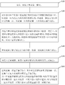
- FIG. 1 is a flow chart showing a method of fabricating a substrate including a quantum rod film in an embodiment of the present invention
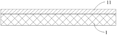
- FIG. 2 is a schematic structural view of forming a first film layer in an embodiment of the present invention
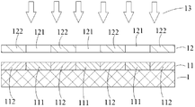
- FIG. 3 is a schematic structural view of forming a first region in an embodiment of the present invention.
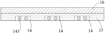
- FIG. 4 is a schematic view showing the structure of forming a quantum rod film in the embodiment of the present invention.
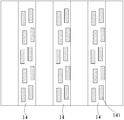
- Figure 5 is a schematic structural view of the top view of Figure 4.
- FIG. 6 is a schematic structural view of a quantum rod film coating adhesive according to an embodiment of the present invention.
- FIG. 7 is a schematic structural view of a quantum rod film transferred onto a second substrate in an embodiment of the present invention.
- FIG. 8 is a schematic structural view showing formation of a quantum rod film on a second substrate in an embodiment of the present invention.
- FIG. 9 is a schematic structural view of a display panel in the prior art.
- FIG. 10 is a schematic structural view of a display panel in an embodiment of the present invention.
- the main object of the present invention is to provide a method for orderly arranging quantum rods on a substrate for the application of quantum rods in display panels.
- a film layer is mainly formed on the bottom plate, and a region having a difference in hydrophilicity and hydrophobicity is disposed on the film layer, and a region having the same hydrophobicity as the quantum rod assembly on the film layer is provided as a slit structure, and the hydrophilicity difference and the slit of the film surface are utilized.
- the effect-induced surface-tuned quantum rod assembly is arranged in an order, and a quantum rod film having an ordered array of quantum rod assemblies is formed on the surface of the bottom plate, and the ordered quantum rod film is transferred to an arbitrary substrate by a transfer technique.
- the surface forms a substrate containing a quantum rod film. Because of The ordered quantum rod assembly realizes the polarization of light, and at the same time, the light of different wavelengths can be obtained by adjusting the size of the quantum rod assembly. Therefore, the substrate containing the quantum rod film realizes the polarizing layer and the color filter in the prior art. The light layer is combined, thereby reducing the thickness of the display panel while reducing the production cost; in addition, since the quantum rod has high conversion efficiency to light, the utilization of light can be improved, and the display panel has a high color gamut and high brightness.
- FIG. 1 is a flow chart showing a method for fabricating a substrate including a quantum rod film in the embodiment, and the manufacturing method includes the following steps:
- step S20 processing the first film layer in step S10 to form a plurality of spaced apart first regions, wherein the first region is a strip structure having a width of a micron order, and other regions on the first film layer are In the second zone, the first zone and the second zone are opposite in water affinity;
- step S30 coating a solution containing a quantum rod assembly onto the first film layer in step S20, the quantum rod assembly having the same affinity for water as the first region, and the size of the quantum rod assembly In the order of micrometers, the quantum rod assemblies are arranged in an orderly manner in the first region to form a quantum rod membrane;
- the quantum rod film includes all of the quantum rod sub-films, and the orthographic projections of the first regions of the different layers of quantum rod sub-films on the second substrate do not coincide, and all of the first regions are in the An orthographic projection on the two substrates covers the entire second substrate plane.
- a first film layer 11 is first formed on the first substrate 1.
- the first film layer 11 is a hydrophobic film layer
- the specific water-repellent film layer means The film layer has hydrophobic properties.
- the hydrophobic film layer is formed by forming a hydrophobic material on a first substrate by coating or other film formation.
- PDMS Polydimethylsiloxane
- the first film layer can also be made into a hydrophilic film layer by using a hydrophilic material.
- the other parts can be correspondingly changed to achieve the object of the present invention.
- the first zone formed in step S20 has Hydrophobic
- quantum rod assemblies should also use hydrophobic quantum rod assemblies. Methods for controlling the hydrophobicity of quantum rod assemblies can be easily obtained in the prior art. To, I will not repeat them here.
- the first film layer 11 in step S10 is processed in step S20 to form a plurality of spaced-apart first regions 111, which are strip-shaped structures having a width of micrometers.
- the other regions on the first film layer 11 are the second regions 112, which are opposite in water to the first region 111 and the second region 112.
- the mask layer 12 is disposed corresponding to the first film layer 11 disposed on the first substrate 1, and the mask plate is provided with a non-occlusion area 121 and an occlusion area 122.
- the non-occlusion region 121 allows ultraviolet light to pass, and the shielding region 122 blocks the passage of ultraviolet light; therefore, the first film layer 11 corresponds to the non-occlusion region 121.
- the region forms the first region 111 (ie, the position corresponding to the first region 111 on the first film layer 11 is converted into a hydrophilic region under the action of ultraviolet rays, and of course, it may be performed in other manners, for example, on the first film layer 11.
- the position corresponding to the first region 111 is bombarded with ozone or plasma such that the surface CH group of the first region is replaced by a C-OH group, so that the surface of the first region is hydrophilic, that is, the first region is converted into a hydrophilic region).
- the portion of the first film layer 11 corresponding to the occlusion region 122 is not irradiated with ultraviolet light, and the unirradiated second region 112 maintains the original hydrophobic property.
- the width of the first region 111 is from 1 ⁇ m to 20 ⁇ m.
- step S30 a solution containing a quantum rod assembly is applied onto the first film layer 11 in step S20, and the quantum rod assembly and the first region 111 are in contact with water. The same is true, and a layer of quantum rod film 14 is formed. As shown in FIG. 4, the quantum rod assembly 141 in the quantum rod film is arranged in an order corresponding to the first region 111.
- the quantum rod assembly Since the quantum rod assembly has the same affinity for water as the first region, when a solution containing the quantum rod assembly is applied onto the first film layer 11, the quantum rod assembly will gather on the upper side of the first region 111; Further, since the width of the first region 111 is on the order of micrometers, that is, the first region 111 corresponds to a slit of a micron order, the effect of inducing the slit causes the quantum rod assembly to be sequentially arranged on the upper side of the first region. Thereby, a quantum rod film as shown in FIGS. 4 and 5 is obtained.
- the coating mode can be selected, for example, by spin coating, slit coating, or ink jet printing. Among them, a preferred coating method is slit coating.
- the quantum rod assembly 141 is a rod-like structure which is large in one dimension and small in two dimensions.
- the size of the quantum rod assembly referred to in the present invention is determined by the dimension in a dimension having a smaller size. .
- the size of the quantum rod assembly 141 in the embodiment of the present invention is on the order of micrometers, which means that the dimension of the quantum rod assembly 141 having a smaller size is on the order of micrometers.
- the quantum rod assembly has a size of from 0.5 ⁇ m to 20 ⁇ m.
- the solution containing the quantum rod assembly can be prepared prior to use, in the present embodiment
- the water-soluble quantum rods are selected, and the size of the quantum rods is generally on the order of nanometers, for example, 1 nm to 100 nm.
- the following is a preparation method of the solution of the quantum rod assembly in the embodiment of the present invention:
- the polar solvent can be water, ethanol, ethylene glycol and mixtures thereof. Of course, there are many other suitable polar solvents, which will not be described here.
- the material of the water-soluble quantum rod in the present invention may be selected from CdX, PbX, ZnX, HgX, GaX, InX (X in the above formula may be S, Se or Te) and a mixture of any of the above materials, which reacts with the above materials.
- the ligand is a common water-soluble surface ligand (the ligand may be thioglycolic acid, mercaptopropionic acid, mercaptoalanine or decylundecanoic acid, glutathione, etc.).
- the ligand may be thioglycolic acid, mercaptopropionic acid, mercaptoalanine or decylundecanoic acid, glutathione, etc.
- step S40 the bonding glue 15 is applied onto the quantum rod film 14, and the second substrate 16 is attached to the bonding glue; before the application of the bonding glue 15, the coating is performed.
- the hydrophilic region of the first film layer 11 is passivated by HDMS (Hexamethyldisilazane, hexamethyldisilazane) such that the hydroxyl group of the first region is substituted with a methyl group.
- the result of the passivation treatment is to reduce the surface energy of the hydrophilic region, thereby facilitating the coating of the adhesive.
- the adhesive 15 material in the present invention may be: a urethane viscous adhesive, an acrylic viscous adhesive, a rubber viscous adhesive (such as SBR, styrene-butadiene rubber), and a polyvinyl ether viscous adhesive.
- Other adhesive materials can also be applied to the present invention and will not be described herein.
- the first substrate 1 is peeled off in step S50, and the first layer of quantum rod sub-film 14 is transferred onto the second substrate 16;
- step S60 At least steps are repeated on the first layer of quantum rod sub-film 14 in step S60.
- a second layer of quantum rod film 17 is formed on the second substrate 16.
- the quantum rod film includes all of the first layer of quantum rod film 14 and the second layer of quantum rod film 17, and the orthographic projections of the first regions of the different layers of quantum rod films on the second substrate 16 do not coincide, all An orthographic projection of the first region on the second substrate covers the entire plane of the second substrate 16.
- the two layers of quantum rod films formed on the second substrate 16 in this embodiment collectively constitute a quantum rod film, and the quantum rod assemblies in the quantum rod film are arranged in an orderly manner.
- FIG. 9 is a schematic structural diagram of a display panel in the prior art, including a first substrate 21, a second substrate 22 disposed corresponding to the first substrate 21, and disposed on the first substrate 21 and the second substrate 22.
- the first liquid crystal layer 23 is generally provided with a first polarizer 24 and a second polarizer 25 on the surfaces of the first substrate 21 and the second substrate 22 away from the liquid crystal layer 23; the display panel structure shown in FIG.
- the first substrate 21 further includes a substrate 211 and a color filter layer 212.
- the display panel of course includes other parts such as an alignment film layer, a plastic frame, and a TFT, etc.
- the common knowledge in the art can be set by a person skilled in the art, and details are not described herein again.
- the display surface is prepared by using the method for preparing a substrate containing a quantum rod film according to an embodiment of the present invention (corresponding to the first embodiment in FIG. 9 A substrate 21) in which the quantum rod film in place replaces the color filter layer 212 and the first polarizer 24 in the color filter substrate.
- the display panel in this embodiment includes an upper substrate 31, a lower substrate 32 disposed corresponding to the upper substrate 31, and a liquid crystal layer 33 disposed between the upper substrate 31 and the lower substrate 32.
- a lower polarizer 34 is disposed on a surface away from the liquid crystal layer 33.
- the upper substrate 31 includes a substrate 311 and a quantum rod film 312 fabricated on the substrate in accordance with the present invention.
- the quantum rod film of the present invention can also be applied to other display panels, such as a COA type display panel (COA, fully called color filter on array), in which color filter layers are arranged in an array.
- COA COA type display panel
- the quantum rod film of the present invention can replace the color filter layer on the array substrate, and the polarizer on the array substrate side can be omitted.
- quantum rods Like quantum dots, quantum rods have the characteristics of being illuminated by light, and the emission spectrum has a narrow half-wave width and good temperature stability.
- the size of the quantum rod assembly can be adjusted to emit light of different wavelengths. Therefore, when the quantum rod film is used as a color filter layer, the quantum rod assembly of different sizes corresponding to different regions of the panel can be displayed as needed, thereby achieving the effect of the color filter layer.
- the different sizes of the quantum rod assemblies in the Ming Dynasty enable the adjustment of the size of the quantum rods so that when the light is irradiated onto the quantum rod assemblies of different sizes, light of different wavelengths is emitted from the quantum rod assembly.
- the color gamut of the liquid crystal display panel on the market is generally 70%. Therefore, the liquid crystal display panel in the implementation of the present invention is 30% higher than the color gamut of the liquid crystal display panel.
Landscapes
- Physics & Mathematics (AREA)
- Nonlinear Science (AREA)
- Mathematical Physics (AREA)
- Chemical & Material Sciences (AREA)
- Crystallography & Structural Chemistry (AREA)
- General Physics & Mathematics (AREA)
- Optics & Photonics (AREA)
- Optical Filters (AREA)
- Polarising Elements (AREA)
Abstract
一种包含量子棒膜的基板及其制作方法、显示面板,量子棒膜中包含的量子棒组装体(141)在基板上有序排列,同时可以通过调整量子棒组装体(141)的尺寸得到不同波长的光。量子棒膜相当于现有技术中的偏光层和彩色滤光层结合,因而降低显示面板的厚度同时降低生产成本。另外由于量子棒对光的转换效率很高,因此可以提高光的利用率,使得显示面板具有高色域和高亮度。
Description
相关申请的交叉引用
本申请要求享有于2017年06月07日提交的名称为“包含量子棒膜的基板及其制作方法、显示面板”的中国专利申请CN201710423427.6的优先权,该申请的全部内容通过引用并入本文中。
本发明涉及显示技术领域,具体涉及一种包含量子棒膜的基板及其制作方法、显示面板。
随着显示技术的快速发展,液晶显示已经成为目前应用最广泛的显示技术之一,人们对显示技术的要求也越来越高。因此,轻薄、高色域和高亮度也成为目前显示技术重要的发展方向。
在现有技术中的显示面板,一般包括第一基板,与第一基板对应设置的第二基板,以及设置于第一基板和第二基板之间的液晶层,在第一基板和第二基板远离液晶层的面上一般还分别设置有第一偏光片和第二偏光片;在第一基板或者第二基板还包括有彩色滤光层。按照滤光层以及液晶的偏转结果从液晶面板中射出的光线的颜色,从而实现对于画面的显示作用。但是随着液晶显示技术的发展,对于显示面板的厚度、色域以及亮度的要求越来越高。因此,相对于现有技术更加轻薄、色域高并且亮度高的显示面板成为众多生产者的研发方向。
量子点(Quantum Dots,QD),又可以称为微米晶,由粒径介于1~20nm之间的微米颗粒组成。由于电子和空穴被量子限域效应的影响,量子点连续的能带结构被分立成独立能级结构,量子点在受到激发后可以发射荧光。量子点的发生光谱主要由量子点的粒径大小来控制,因此可以通过改变量子点的粒径来实现其发射光谱的调节。同时,量子点的光转换效率很高,可以提高光的利用率。量子棒QR(Quantum rod)是二维微米材料,具有量子点的调光效应,即通过调节量子
棒的尺寸可以改变量子棒受到激发而得到的光谱。而且有序排列的量子棒还可以实现光的偏振。但如何实现QR的有序排列,利用QR实现光的偏振一直难以实现。
发明内容
为了解决现有技术中的问题,本发明提供的包含量子棒膜的基板及其制作方法、显示面板。
首先,本发明提供一种包含量子棒膜的基板的制作方法,包括以下步骤:
S10:在第一衬底上形成第一膜层;
S20:对步骤S10中的第一膜层进行处理形成多个间隔设置的第一区,所述第一区为宽度为微米级的条状结构,所述第一膜层上的其他区域为第二区,所述第一区和所述第二区对水的亲疏性相反;
S30:将包含量子棒组装体的溶液涂布到步骤S20中的第一膜层上,所述量子棒组装体与所述第一区对水的亲疏性相同,所述量子棒组装体的尺寸为微米级,所述量子棒组装体在所述第一区上有序排列,形成一层量子棒子膜;
S40:在所述量子棒子膜上涂布贴合胶,将第二衬底贴合到贴合胶上;
S50:将第一衬底剥离,将第一层量子棒子膜转到所述第二衬底上;
S60:在所述第一层量子棒子膜上,至少重复步骤S10至步骤S40一次,在第二衬底上形成至少两层量子棒子膜;
其中,所述量子棒膜包括所有所述的量子棒子膜,制作不同层量子棒子膜的第一区在所述第二衬底上的正投影不重合,所有所述第一区在所述第二衬底上的正投影覆盖整个第二衬底平面。
本发明通过将第一区设置为宽度微米级的条状结构,同时使得第一区与量子棒组装体对水具有相同的亲疏性,通过第一区的诱导效应使得量子棒组装体在第一区上有序排列,使得得到的量子棒膜同时具有了彩色滤光层和偏光层的效果,因此,可以使得应用该方法制作的基板更薄,使得包括所述基板的显示面板更加轻薄,色域高并且亮度高。
作为对上述制作方法的进一步改进,所述的第一膜层为亲水膜层,所述第一区为疏水区域,所述量子棒组装体具有疏水性,所述量子棒组装体的尺寸为0.5μm至20μm,所述第一区的宽度为1μm至20μm。
作为对上述制作方法的进一步改进,所述的第一膜层为疏水膜层,所述第一区为亲水区域,所述量子棒组装体具有亲水性,所述量子棒组装体的尺寸为0.5μm至20μm,所述第一区的宽度为1μm至20μm。
本发明中的第一区的宽度的范围为一个优选的范围,在此范围内的可以容纳不同尺寸的量子棒组装体,从而量子棒膜可以根据实际需要发出不同波长的光。
作为对上述制作方法的进一步改进,步骤S10中,所述第一膜层采用聚二甲基硅氧烷形成,步骤S20中,对所述第一膜层的局部区域进行紫外线照射,臭氧或者等离子体处理,使得被处理区烷基链生成羟基,形成所述第一区。采用聚二甲基硅氧烷作为形成第一膜层的材料,从而使得第一区的制作过程更加简单和方便,例如紫外照射,臭氧以及等离子体处理都是本领域常用的技术,因此,可以利用已有的设备达到本发明中的效果,降低了生产和研发的成本。
作为对上述制作方法的进一步改进,步骤S40中在进行贴合胶的涂布之前,用六甲基二硅氮烷对所述第一区进行钝化处理,使得所述第一区羟基被甲基取代。进行贴合胶的涂布之前对第一区进行钝化处理,降低了第一区的表面能,使得贴合胶与量子棒子膜的贴合效果更好。
作为对上述制作方法的进一步改进,所述多个第一区平行设置。第一区的平行设置,从而使得量子棒膜的偏光效果更好。
作为对上述制作方法的进一步改进,步骤S30中采用旋转涂布、狭缝式涂布或喷墨打印的方式进行包含量子棒组装体的溶液的涂布。
本发明还提供一种包含量子棒膜的基板,所述基板根据以上所述的制作方法进行制作。
优选的,所述基板为彩膜基板。将包含量子棒膜的基板作为彩膜基板的优势在于,相对于阵列基板,彩膜基板的结构相对简单,因此,将量子棒膜设置到彩膜基板上,使得工艺更加简单。
另外,本发明还提供一种显示面板,包括:
第一基板,
与第一基板相对设置的第二基板,以及
设置于所述第一基板和所述第二基板之间的液晶层;
其中,所述第一基板为以上所述的包含量子棒膜的基板,在所述第二基板远离液晶层的一侧设置有偏光层。
本发明提供的包含量子棒膜的基板及其制作方法、显示面板,其中的包含的量子棒在基板上有序排列,同时可以通过调整量子棒组装体的尺寸得到不同波长的光。本发明中的量子棒膜相当于现有技术中的偏光层和彩色滤光层结合,因而降低显示面板的厚度同时降低生产成本。另外由于量子棒对光的转换效率很高,因此可以提高光的利用率,使得显示面板具有高色域和高亮度。
在下文中将基于实施例并参考附图来对本发明进行更详细的描述。其中:
图1是本发明实施例中包含量子棒膜的基板的制作方法流程图;
图2是本发明实施例中形成第一膜层的结构示意图;
图3是本发明实施例中形成第一区的结构示意图;
图4是本发明实施例中形成一层量子棒子膜的结构示意图;
图5是图4的俯视方向的结构示意图;
图6是本发明实施例中量子棒子膜涂布贴合胶的结构示意图;
图7是本发明实施例中量子棒子膜转印到第二衬底上的结构示意图;
图8是本发明实施例中第二衬底上形成量子棒膜的结构示意图;
图9是现有技术中一种显示面板结构示意图;
图10是本发明实施例中的显示面板结构示意图。
在附图中,相同的部件使用相同的附图标记。附图并未按照实际的比例。
以下将结合附图对本发明的内容作出详细的说明,下文中的“上”“下”“左”“右”均为相对于图示方向,不应理解为对本发明的限制。本发明中出现的“μm”为长度单位微米,“nm”为长度单位纳米。
本发明的主要目的是对于量子棒在显示面板中的应用,提供一种在基板上将量子棒有序排列的方法。主要在底板形成一个膜层,在膜层上设置有亲疏水性差异的区域,膜层上与量子棒组装体的亲疏水性相同的区域设置为狭缝结构,利用膜面的亲疏水性差异和狭缝效应诱导经过表面修饰的量子棒组装体进行有序排列,在底板表面形成具有有序排列的量子棒组装体的量子棒膜,同时通过转印技术将有序排列量子棒膜转印到任意基板表面,形成包含量子棒膜的基板。由于有
序排列的量子棒组装体在实现光的偏振,同时可以通过调整量子棒组装体的尺寸得到不同波长的光,因此包含量子棒膜的基板,实现了将现有技术中的偏光层和彩色滤光层结合,因而降低显示面板的厚度同时降低生产成本;另外由于量子棒对光的转换效率很高,因此可以提高光的利用率,使得显示面板具有高色域和高亮度。
如图1所示为本实施例中的包含量子棒膜的基板的制作方法的流程图,所述的制作方法包括以下步骤:
S10:在第一衬底上形成第一膜层;
S20:对步骤S10中的第一膜层进行处理形成多个间隔设置的第一区,所述第一区为宽度为微米级的条状结构,所述第一膜层上的其他区域为第二区,所述第一区和所述第二区对水的亲疏性相反;
S30:将包含量子棒组装体的溶液涂布到步骤S20中的第一膜层上,所述量子棒组装体与所述第一区对水的亲疏性相同,所述量子棒组装体的尺寸为微米级,所述量子棒组装体在所述第一区中有序排列,形成一层量子棒子膜;
S40:在所述量子棒子膜上涂布贴合胶,将第二衬底贴合到贴合胶上;
S50:将第一衬底剥离,将第一层量子棒子膜转到所述第二衬底上;
S60:在所述第一层量子棒子膜上,至少重复步骤S10至步骤S40一次,在第二衬底上形成至少两层量子棒子膜;
其中,所述量子棒膜包括所有所述的量子棒子膜,制作不同层量子棒子膜的第一区在所述第二衬底上的正投影不重合,所有所述第一区在所述第二衬底上的正投影覆盖整个第二衬底平面。
下面结合具体的附图以及具体的例子,上述的步骤进行更为详细的阐述。
如图2所示,在步骤S10中,首先在第一衬底1上形成第一膜层11,在本实施例中的第一膜层11为疏水膜层,具体的疏水膜层是指该膜层具有疏水性质。疏水膜层是通过将疏水性材料采用涂布或者其他的成膜方式在第一衬底上成膜形成的。具体的例如可以采用PDMS(Polydimethylsiloxane,聚二甲基硅氧烷)作为形成该疏水膜层的疏水性材料。当然,也可以采用亲水性材料将第一膜层制作成亲水膜层,该种情况下其他部分作相应的改变即可实现本发明的目的,例如在步骤S20中形成的第一区具有疏水性,量子棒组装体也应该选用具有疏水性的量子棒组装体,控制量子棒组装体的亲疏水性的方法现有技术中可以很容易地得
到,在此不再赘述。
如图3所示,在步骤S20中对步骤S10中的第一膜层11进行处理形成多个间隔设置的第一区111,所述第一区111为宽度为微米级的条状结构,所述第一膜层11上的其他区域为第二区112,所述第一区111和所述第二区112对水的亲疏性相反。在本实施例中,如图2所示,使用掩膜板12与设置在第一衬底1上的第一膜层11对应设置,掩膜板上设置有非遮挡区121和遮挡区122,在采用紫外13照射的方法对第一膜层进行处理时,非遮挡区121允许紫外光通过,遮挡区122阻挡紫外光的通过;因此,第一膜层11上与非遮挡区121对对应的区域形成第一区111(即第一膜层11上与第一区111对应的位置在在紫外线的作用下转变为亲水区域,当然也可以采用其他的方式进行,例如第一膜层11上与第一区111对应的位置用臭氧或者等离子体进行轰击,使得第一区表面C-H基团被C-OH基团取代,使得第一区表面具有亲水性,即第一区转变为亲水区域)。第一膜层11上与遮挡区122对应的部分未收到紫外光的照射,未被照射的第二区112保持原有的疏水性能。优选的,第一区111的宽度为1μm至20μm。
如图4所示,在步骤S30中,将包含量子棒组装体的溶液涂布到步骤S20中的第一膜层11上,所述量子棒组装体与所述第一区111对水的亲疏性相同,形成一层量子棒子膜14,如图4中所示,量子棒子膜中的量子棒组装体141在于第一区111对应的位置上有序排列。由于量子棒组装体与第一区对水的亲疏性相同,当将包含量子棒组装体的溶液涂布到第一膜层11上时,量子棒组装体会聚集在第一区111的上侧;又由于第一区111的宽度为微米级,即第一区111相当于微米级的狭缝,狭缝的诱导效应会使得量子棒组装体在第一区上侧有序排列。从而得到如图4和图5所示的量子棒子膜。在一些实施例中,可以对涂布方式进行选择,例如可以采用旋转涂布、狭缝式涂布或喷墨打印等方式进行。其中优选的涂布方式为狭缝涂布。
量子棒组装体141为棒状结构,其在一个维度上尺寸较大,另外两个维度上尺寸较小,本发明所指的量子棒组装体的尺寸以具有较小尺寸的维度上的尺寸为准。例如本发明实施例中的量子棒组装体141的尺寸为微米级,指的是量子棒组装体141具有较小尺寸的维度上的尺寸为微米级别。优选的,量子棒组装体的尺寸为0.5μm至20μm。
包含量子棒组装体的溶液可以在使用之前进行制备,在本实施例中的量子棒
选用的为水溶性量子棒,量子棒的尺寸一般为纳米级,例如1nm至100nm。以下是本发明实施例中量子棒组装体的溶液的一种制备方法:
(1)对量子棒进行修饰,获得量子棒胶束;具体的,将量子棒溶解到乙二醇水溶液中,在所述溶液中加入辛胺和十八烷基膦酸,混合均匀,除去溶剂获得量子棒胶束。
(2)对量子棒胶束进行自组装,形成微米级的量子棒组装体;具体的,将量子棒胶束溶解到氯仿中,加入一定量的十二烷基三甲基溴化铵,通氩气蒸发除去氯仿,再将剩余物加入到乙二醇中,剧烈搅拌10分钟形成量子棒组装体,然后加入二硫醇官能化的Tween-20(吐温-20)稳定量子棒组装体。
(3)形成包含量子棒组装体的溶液;具体的,将形成的量子棒组装体进行分离和提纯,在将提纯得到的量子棒组装体分散到不同的极性溶剂中,所述极性溶剂可以为水、乙醇、乙二醇及其混合物,当然其他适用的极性溶剂还有很多,在此不再赘述。
本发明中的水溶性量子棒的材料可以选自CdX,PbX,ZnX,HgX,GaX,InX(以上分子式中的X可以为S,Se或Te)及以上任意材料的混合物,与上述材料反应的配体为常见的水溶性表面配体(所述配体可以为巯基乙酸,巯基丙酸,巯基丙氨酸或巯基十一酸及谷胱甘肽等)。当然其他可以可适用于本发明的量子棒材料以及表面配体在也可适用于本发明,在此不再赘述。
如图6所示,在步骤S40中,在量子棒子膜14上涂布贴合胶15,将第二衬底16贴合到贴合胶上;在进行贴合胶15的涂布之前,用HDMS(Hexamethyldisilazane,六甲基二硅氮烷)对第一膜层11的亲水区进行钝化处理,使得所述第一区羟基被甲基取代。钝化处理的结果是使得亲水区的表面能降低,从而有利于贴合胶的涂布。
本发明中的粘合胶15材料可以为:氨酯感压黏剂、丙烯酸感压黏剂、橡胶感压黏剂(如SBR,苯乙烯-丁二烯橡胶)、聚乙烯醚感压黏剂、聚异丁烯感压黏剂、环氧感压黏剂、酚类感压黏剂、硅感压黏剂、聚酯感压黏剂以及上述材料中任意材料的混合物。其他的贴合胶材料亦可适用于本发明,在此不再赘述。
如图7所示,在步骤S50中将第一衬底1剥离,将第一层量子棒子膜14转到所述第二衬底16上;
如图8所示,在步骤S60中在所述第一层量子棒子膜14上,至少重复步骤
S10至步骤S40一次,在第二衬底16上形成第二层量子棒子膜17。量子棒膜包括所有第一层量子棒子膜14和第二层量子棒子膜17,用于制作不同层量子棒子膜的第一区在所述第二衬底16上的正投影不重合,所有所述第一区在所述第二衬底上的正投影覆盖整个第二衬底16平面。
本实施例中在第二衬底16上形成的两层量子棒子膜共同组成量子棒膜,该量子棒膜中的量子棒组装体有序排列。
如图9所示为现有技术中一种显示面板的结构示意图,包括第一基板21,与第一基板21对应设置的第二基板22,以及设置在第一基板21和第二基板22之间的液晶层23,在第一基板21和第二基板22远离液晶层23的面上一般还分别设置有第一偏光片24和第二偏光片25;由图9中所示的显示面板结构中,第一基板21还包括衬底211和彩色滤光层212。本发明中的仅仅对于本发明的改进涉及的部分进行具体的描述,其他部份不做详述;显示面板当然还包括的其他部分,例如取向膜层、胶框以及TFT等,该部分内容作为本领域的公知常识本领域技术人员可以自行进行设置,在此不再赘述。
如图10所示,为本发明中的显示面板的一个实施例,该显示面用本发明实施例中的包含量子棒膜的基板的制备方法制备彩膜基板(相当于如图9中的第一基板21),该实施例中其中的量子棒膜代替了彩膜基板中的彩色滤光层212和第一偏光片24。具体如图10所示,本实施例中的显示面板包括上基板31,与上基板31对应设置的下基板32,以及设置在上基板31和下基板32之间的液晶层33,在下基板32远离液晶层33的面上设置有下偏光片34。在本实施例中,上基板31包括衬底311和根据本发明制作在衬底上的量子棒膜312。
当然本发明中的量子棒膜也可以适用于其他情况的显示面板,例如COA型显示面板(COA,全称为color filter on array),在该种类型的显示面板中彩色滤光片层设置在阵列基板上,因此,本发明中的量子棒膜可以代替阵列基板上的彩色滤光片层,同时也可以省去阵列基板侧的偏光片。本领域技术人员可以根据需要进行设置,在此无需赘述。
量子棒与量子点一样具有受到光照射而发光的特性,且发射光谱半波宽很窄,温度稳定性好。在实际使用时可以通过调整量子棒组装体的尺寸使其发出不同波长的光。因此,将量子棒膜作为彩色滤光层使用时,可以根据需要显示面板的不同区域对应与不同尺寸的量子棒组装体,从而起到彩色滤光层的效果。本发
明中的量子棒组装体不同尺寸即实现了对于量子棒的尺寸的调整,从而当光照射到不同尺寸的量子棒组装体时,从量子棒组装体发射出不同波长的光。有研究显示,量子点作为发光材料与颜料或者荧光粉比较,其色域(NTSC,National Television Standard Committee)可大于100%。目前市场上液晶显示面板色域一般为70%,因此,本发明实施中的液晶显示面板比液晶显示面板色域高出30%。
虽然已经参考优选实施例对本发明进行了描述,但在不脱离本发明的范围的情况下,可以对其进行各种改进并且可以用等效物替换其中的部件。尤其是,只要不存在结构冲突,各个实施例中所提到的各项技术特征均可以任意方式组合起来。本发明并不局限于文中公开的特定实施例,而是包括落入权利要求的范围内的所有技术方案。
Claims (18)
- 一种包含量子棒膜的基板的制作方法,包括以下步骤:S10:在第一衬底上形成第一膜层;S20:对步骤S10中的第一膜层进行处理形成多个间隔设置的第一区,所述第一区为宽度为微米级的条状结构,所述第一膜层上的其他区域为第二区,所述第一区和所述第二区对水的亲疏性相反;S30:将包含量子棒组装体的溶液涂布到步骤S20中的第一膜层上,所述量子棒组装体与所述第一区对水的亲疏性相同,所述量子棒组装体的尺寸为微米级,所述量子棒组装体在所述第一区上有序排列,形成一层量子棒子膜;S40:在所述量子棒子膜上涂布贴合胶,将第二衬底贴合到贴合胶上;S50:将第一衬底剥离,将第一层量子棒子膜转到所述第二衬底上;S60:在所述第一层量子棒子膜上,至少重复步骤S10至步骤S40一次,在第二衬底上形成至少两层量子棒子膜;其中,所述量子棒膜包括所有所述的量子棒子膜,制作不同层量子棒子膜的第一区在所述第二衬底上的正投影不重合,所有所述第一区在所述第二衬底上的正投影覆盖整个第二衬底平面。
- 根据权利要求1所述的制作方法,其中,所述多个第一区平行设置。
- 根据权利要求2所述的制作方法,其中,步骤S30中采用旋转涂布、狭缝式涂布或喷墨打印的方式进行包含量子棒组装体的溶液的涂布。
- 根据权利要求1所示的制作方法,其中:所述的第一膜层为亲水膜层,所述第一区为疏水区域,所述量子棒组装体具有疏水性,所述量子棒组装体的尺寸为0.5μm至20μm,所述第一区的宽度为1μm至20μm。
- 根据权利要求4所述的制作方法,其中,所述多个第一区平行设置。
- 根据权利要求1所示的制作方法,其中:所述的第一膜层为疏水膜层,所述第一区为亲水区域,所述量子棒组装体具有亲水性,所述量子棒组装体的尺寸为0.5μm至20μm,所述第一区的宽度为1μm至20μm。
- 根据权利要求6所述的制作方法,其中,所述多个第一区平行设置。
- 根据权利要求6所述的制作方法,其中,步骤S40中在进行贴合胶的涂布之前,用六甲基二硅氮烷对所述第一区进行钝化处理,使得所述第一区羟基被甲 基取代。
- 根据权利要求8所述的制作方法,其中,所述多个第一区平行设置。
- 根据权利要求6所述的制作方法,其中,步骤S10中,所述第一膜层采用聚二甲基硅氧烷形成,步骤S20中,对所述第一膜层的局部区域进行紫外线照射,臭氧或者等离子体处理,使得被处理区烷基链生成羟基,形成所述第一区。
- 根据权利要求10所述的制作方法,其中,所述多个第一区平行设置。
- 根据权利要求10所述的制作方法,其中,步骤S40中在进行贴合胶的涂布之前,用六甲基二硅氮烷对所述第一区进行钝化处理,使得所述第一区羟基被甲基取代。
- 根据权利要求12所述的制作方法,其中,所述多个第一区平行设置。
- 根据权利要求13所述的制作方法,其中,步骤S30中采用旋转涂布、狭缝式涂布或喷墨打印的方式进行包含量子棒组装体的溶液的涂布。
- 一种包含量子棒膜的基板,其中,所述基板根据以下方法制作:S10:在第一衬底上形成第一膜层;S20:对步骤S10中的第一膜层进行处理形成多个间隔设置的第一区,所述第一区为宽度为微米级的条状结构,所述第一膜层上的其他区域为第二区,所述第一区和所述第二区对水的亲疏性相反;S30:将包含量子棒组装体的溶液涂布到步骤S20中的第一膜层上,所述量子棒组装体与所述第一区对水的亲疏性相同,所述量子棒组装体的尺寸为微米级,所述量子棒组装体在所述第一区上有序排列,形成一层量子棒子膜;S40:在所述量子棒子膜上涂布贴合胶,将第二衬底贴合到贴合胶上;S50:将第一衬底剥离,将第一层量子棒子膜转到所述第二衬底上;S60:在所述第一层量子棒子膜上,至少重复步骤S10至步骤S40一次,在第二衬底上形成至少两层量子棒子膜;其中,所述量子棒膜包括所有所述的量子棒子膜,制作不同层量子棒子膜的第一区在所述第二衬底上的正投影不重合,所有所述第一区在所述第二衬底上的正投影覆盖整个第二衬底平面。
- 根据权利要求15所述的基板,其中,所述基板为彩膜基板。
- 一种显示面板,包括:第一基板,与第一基板相对设置的第二基板,以及设置于所述第一基板和所述第二基板之间的液晶层;其中,所述第一基板为包含量子棒膜的基板,在所述第二基板远离液晶层的一侧设置有偏光层;所述第一基板根据以下方法制作:S10:在第一衬底上形成第一膜层;S20:对步骤S10中的第一膜层进行处理形成多个间隔设置的第一区,所述第一区为宽度为微米级的条状结构,所述第一膜层上的其他区域为第二区,所述第一区和所述第二区对水的亲疏性相反;S30:将包含量子棒组装体的溶液涂布到步骤S20中的第一膜层上,所述量子棒组装体与所述第一区对水的亲疏性相同,所述量子棒组装体的尺寸为微米级,所述量子棒组装体在所述第一区上有序排列,形成一层量子棒子膜;S40:在所述量子棒子膜上涂布贴合胶,将第二衬底贴合到贴合胶上;S50:将第一衬底剥离,将第一层量子棒子膜转到所述第二衬底上;S60:在所述第一层量子棒子膜上,至少重复步骤S10至步骤S40一次,在第二衬底上形成至少两层量子棒子膜;其中,所述量子棒膜包括所有所述的量子棒子膜,制作不同层量子棒子膜的第一区在所述第二衬底上的正投影不重合,所有所述第一区在所述第二衬底上的正投影覆盖整个第二衬底平面。
- 根据权利要求17所述的显示面板,其中,所述第一基板为彩膜基板。
Priority Applications (1)
| Application Number | Priority Date | Filing Date | Title |
|---|---|---|---|
| US15/550,135 US10649278B2 (en) | 2017-06-07 | 2017-07-04 | Sustrate comprising quantum rod film and method for manufacturing the same, display panel |
Applications Claiming Priority (2)
| Application Number | Priority Date | Filing Date | Title |
|---|---|---|---|
| CN201710423427.6A CN107065308B (zh) | 2017-06-07 | 2017-06-07 | 包含量子棒膜的基板及其制作方法、显示面板 |
| CN201710423427.6 | 2017-06-07 |
Publications (1)
| Publication Number | Publication Date |
|---|---|
| WO2018223472A1 true WO2018223472A1 (zh) | 2018-12-13 |
Family
ID=59615940
Family Applications (1)
| Application Number | Title | Priority Date | Filing Date |
|---|---|---|---|
| PCT/CN2017/091663 Ceased WO2018223472A1 (zh) | 2017-06-07 | 2017-07-04 | 包含量子棒膜的基板及其制作方法、显示面板 |
Country Status (3)
| Country | Link |
|---|---|
| US (1) | US10649278B2 (zh) |
| CN (1) | CN107065308B (zh) |
| WO (1) | WO2018223472A1 (zh) |
Families Citing this family (7)
| Publication number | Priority date | Publication date | Assignee | Title |
|---|---|---|---|---|
| CN107513304B (zh) * | 2017-08-23 | 2021-06-08 | 南方科技大学 | 一种基于量子棒定向排列的荧光偏振薄膜的制备方法 |
| CN108957828A (zh) * | 2018-06-19 | 2018-12-07 | 南京中电熊猫平板显示科技有限公司 | 一种显示装置、显示面板及其制造方法 |
| CN109786431B (zh) | 2019-02-25 | 2021-10-22 | 京东方科技集团股份有限公司 | 显示基板及其制备方法、和显示装置 |
| CN114341719A (zh) * | 2019-08-16 | 2022-04-12 | 珠海市柔美科技有限公司 | Lcd用光取向量子棒增强膜的钝化层 |
| CN110824769B (zh) * | 2019-10-30 | 2021-02-02 | 深圳市华星光电半导体显示技术有限公司 | 透明显示装置 |
| CN113122259A (zh) * | 2019-12-30 | 2021-07-16 | Tcl集团股份有限公司 | 一种复合材料及其制备方法、偏振片与液晶显示器 |
| CN111257989A (zh) * | 2020-03-04 | 2020-06-09 | Tcl华星光电技术有限公司 | 偏光膜及其制备方法与显示面板 |
Citations (8)
| Publication number | Priority date | Publication date | Assignee | Title |
|---|---|---|---|---|
| JP2010085337A (ja) * | 2008-10-01 | 2010-04-15 | Kobe Univ | ナノワイヤを用いた微細流路の製造方法 |
| US20140362556A1 (en) * | 2013-06-11 | 2014-12-11 | Samsung Display Co., Ltd. | Quantum rod sheet, backlight unit, display device and manufacturing method thereof |
| CN104992631A (zh) * | 2015-07-29 | 2015-10-21 | 深圳市华星光电技术有限公司 | 量子棒膜的制造方法及量子棒发光显示装置 |
| CN105093677A (zh) * | 2015-08-11 | 2015-11-25 | 深圳市华星光电技术有限公司 | 液晶显示器及其液晶显示模组 |
| CN105301828A (zh) * | 2015-11-18 | 2016-02-03 | 深圳市华星光电技术有限公司 | 液晶显示装置及其制作方法 |
| CN105404047A (zh) * | 2015-12-04 | 2016-03-16 | 深圳市华星光电技术有限公司 | Coa型液晶显示面板的制作方法及coa型液晶显示面板 |
| CN105403945A (zh) * | 2016-01-04 | 2016-03-16 | 京东方科技集团股份有限公司 | 一种偏振片及其制作方法、显示面板 |
| CN105549260A (zh) * | 2016-03-08 | 2016-05-04 | 京东方科技集团股份有限公司 | 一种量子棒结构及其制作方法 |
Family Cites Families (10)
| Publication number | Priority date | Publication date | Assignee | Title |
|---|---|---|---|---|
| KR101281877B1 (ko) * | 2006-09-18 | 2013-07-03 | 엘지디스플레이 주식회사 | 칼라 필터 어레이 패널 및 그 제조 방법 |
| CN101398561B (zh) * | 2007-09-29 | 2011-12-07 | 奇美电子股份有限公司 | 彩色滤光片基板及其制造方法以及应用它的液晶显示面板 |
| CN101376599A (zh) * | 2008-09-25 | 2009-03-04 | 上海交通大学 | 纳米粒子有序单层和多层薄膜的制备方法 |
| CN102502485A (zh) * | 2011-11-10 | 2012-06-20 | 中山大学 | 一种纳米材料的图形化工艺方法 |
| CN102664237A (zh) * | 2012-04-27 | 2012-09-12 | 中国科学院理化技术研究所 | 一种定向及图案化排列一维有机纳米材料的方法 |
| CN103091895B (zh) * | 2013-01-22 | 2015-12-09 | 北京京东方光电科技有限公司 | 一种显示装置及制备方法 |
| CN103854723B (zh) * | 2014-02-20 | 2017-04-12 | 中山大学 | 一种应用有序导电薄膜的器件 |
| KR102373327B1 (ko) * | 2015-04-30 | 2022-03-11 | 삼성디스플레이 주식회사 | 액정 표시 장치 및 그 구동 방법 |
| CN105152125B (zh) * | 2015-08-10 | 2017-04-19 | 中山大学 | 一种基于微沟道结构的微纳米材料有序自组装图形化方法 |
| KR102504125B1 (ko) * | 2015-10-13 | 2023-02-28 | 삼성디스플레이 주식회사 | 편광 선택 컬러 필터 및 이를 구비하는 표시 장치 |
-
2017
- 2017-06-07 CN CN201710423427.6A patent/CN107065308B/zh active Active
- 2017-07-04 US US15/550,135 patent/US10649278B2/en active Active
- 2017-07-04 WO PCT/CN2017/091663 patent/WO2018223472A1/zh not_active Ceased
Patent Citations (8)
| Publication number | Priority date | Publication date | Assignee | Title |
|---|---|---|---|---|
| JP2010085337A (ja) * | 2008-10-01 | 2010-04-15 | Kobe Univ | ナノワイヤを用いた微細流路の製造方法 |
| US20140362556A1 (en) * | 2013-06-11 | 2014-12-11 | Samsung Display Co., Ltd. | Quantum rod sheet, backlight unit, display device and manufacturing method thereof |
| CN104992631A (zh) * | 2015-07-29 | 2015-10-21 | 深圳市华星光电技术有限公司 | 量子棒膜的制造方法及量子棒发光显示装置 |
| CN105093677A (zh) * | 2015-08-11 | 2015-11-25 | 深圳市华星光电技术有限公司 | 液晶显示器及其液晶显示模组 |
| CN105301828A (zh) * | 2015-11-18 | 2016-02-03 | 深圳市华星光电技术有限公司 | 液晶显示装置及其制作方法 |
| CN105404047A (zh) * | 2015-12-04 | 2016-03-16 | 深圳市华星光电技术有限公司 | Coa型液晶显示面板的制作方法及coa型液晶显示面板 |
| CN105403945A (zh) * | 2016-01-04 | 2016-03-16 | 京东方科技集团股份有限公司 | 一种偏振片及其制作方法、显示面板 |
| CN105549260A (zh) * | 2016-03-08 | 2016-05-04 | 京东方科技集团股份有限公司 | 一种量子棒结构及其制作方法 |
Also Published As
| Publication number | Publication date |
|---|---|
| CN107065308B (zh) | 2020-07-03 |
| US20200004081A1 (en) | 2020-01-02 |
| US10649278B2 (en) | 2020-05-12 |
| CN107065308A (zh) | 2017-08-18 |
Similar Documents
| Publication | Publication Date | Title |
|---|---|---|
| WO2018223472A1 (zh) | 包含量子棒膜的基板及其制作方法、显示面板 | |
| CN105301827B (zh) | 量子点彩膜基板的制备方法及量子点彩膜基板 | |
| US11467325B2 (en) | Optical filter and manufacturing method therefor, display substrate, and display apparatus | |
| KR102023795B1 (ko) | 나노로드들의 형광 에미션에 기반한 3차원 디스플레이 시스템 | |
| KR101793741B1 (ko) | 표시장치 | |
| WO2017080078A1 (zh) | 量子点彩膜基板的制备方法及量子点彩膜基板 | |
| US9804489B2 (en) | Method for manufacturing quantum dot color filter | |
| US9897912B2 (en) | Color filter film manufacturing method and color filter film | |
| DE112014004238B4 (de) | Dünnfilm-Wellenlängenkonverter und Verfahren zu deren Herstellung | |
| WO2017092131A1 (zh) | 彩膜基板的制作方法及液晶显示装置 | |
| CN107689388B (zh) | 一种显示面板及其制造方法 | |
| CN105278155A (zh) | 量子点彩膜基板的制作方法 | |
| WO2014183334A1 (zh) | 液晶显示屏、显示装置及单色量子点层的制备方法 | |
| US20170254934A1 (en) | Method for patterning quantum dot layer and method for manufacturing quantum dot color filter | |
| US20160116650A1 (en) | Color filter substrate and its manufacturing method, display panel and its manufacturing method, and display device | |
| CN109814191B (zh) | 一种像素化量子点滤光膜的制备方法 | |
| TWI815987B (zh) | 硬化性組成物、膜、積層體及顯示裝置 | |
| TWI850494B (zh) | 光轉換層形成用噴墨墨水組成物、光轉換層及彩色濾光片 | |
| CN109560206B (zh) | 胶体量子点薄膜图案化方法 | |
| CN105511155B (zh) | 量子点彩色滤光片的制造方法 | |
| KR20170123600A (ko) | 표시장치 | |
| CN121444636A (zh) | 电荷传输性墨组合物和表面处理金属氧化物纳米粒子溶胶 | |
| CN205067782U (zh) | 滤光片、显示基板及显示装置 | |
| CN108089374A (zh) | 一种量子点膜片阵列及其应用 | |
| WO2020042641A1 (zh) | 一种led显示器件的制备方法及led显示器件 |
Legal Events
| Date | Code | Title | Description |
|---|---|---|---|
| 121 | Ep: the epo has been informed by wipo that ep was designated in this application |
Ref document number: 17912995 Country of ref document: EP Kind code of ref document: A1 |
|
| NENP | Non-entry into the national phase |
Ref country code: DE |
|
| 122 | Ep: pct application non-entry in european phase |
Ref document number: 17912995 Country of ref document: EP Kind code of ref document: A1 |