WO2018207652A1 - 防塵レンズ及びその製造方法 - Google Patents
防塵レンズ及びその製造方法 Download PDFInfo
- Publication number
- WO2018207652A1 WO2018207652A1 PCT/JP2018/017119 JP2018017119W WO2018207652A1 WO 2018207652 A1 WO2018207652 A1 WO 2018207652A1 JP 2018017119 W JP2018017119 W JP 2018017119W WO 2018207652 A1 WO2018207652 A1 WO 2018207652A1
- Authority
- WO
- WIPO (PCT)
- Prior art keywords
- film
- conductive film
- lens
- titanium oxide
- dustproof
- Prior art date
- Legal status (The legal status is an assumption and is not a legal conclusion. Google has not performed a legal analysis and makes no representation as to the accuracy of the status listed.)
- Ceased
Links
Images


Classifications
-
- C—CHEMISTRY; METALLURGY
- C23—COATING METALLIC MATERIAL; COATING MATERIAL WITH METALLIC MATERIAL; CHEMICAL SURFACE TREATMENT; DIFFUSION TREATMENT OF METALLIC MATERIAL; COATING BY VACUUM EVAPORATION, BY SPUTTERING, BY ION IMPLANTATION OR BY CHEMICAL VAPOUR DEPOSITION, IN GENERAL; INHIBITING CORROSION OF METALLIC MATERIAL OR INCRUSTATION IN GENERAL
- C23C—COATING METALLIC MATERIAL; COATING MATERIAL WITH METALLIC MATERIAL; SURFACE TREATMENT OF METALLIC MATERIAL BY DIFFUSION INTO THE SURFACE, BY CHEMICAL CONVERSION OR SUBSTITUTION; COATING BY VACUUM EVAPORATION, BY SPUTTERING, BY ION IMPLANTATION OR BY CHEMICAL VAPOUR DEPOSITION, IN GENERAL
- C23C14/00—Coating by vacuum evaporation, by sputtering or by ion implantation of the coating forming material
- C23C14/06—Coating by vacuum evaporation, by sputtering or by ion implantation of the coating forming material characterised by the coating material
- C23C14/08—Oxides
-
- G—PHYSICS
- G02—OPTICS
- G02B—OPTICAL ELEMENTS, SYSTEMS OR APPARATUS
- G02B1/00—Optical elements characterised by the material of which they are made; Optical coatings for optical elements
- G02B1/10—Optical coatings produced by application to, or surface treatment of, optical elements
- G02B1/11—Anti-reflection coatings
- G02B1/113—Anti-reflection coatings using inorganic layer materials only
- G02B1/115—Multilayers
- G02B1/116—Multilayers including electrically conducting layers
-
- G—PHYSICS
- G02—OPTICS
- G02B—OPTICAL ELEMENTS, SYSTEMS OR APPARATUS
- G02B1/00—Optical elements characterised by the material of which they are made; Optical coatings for optical elements
- G02B1/10—Optical coatings produced by application to, or surface treatment of, optical elements
- G02B1/16—Optical coatings produced by application to, or surface treatment of, optical elements having an anti-static effect, e.g. electrically conducting coatings
-
- G—PHYSICS
- G02—OPTICS
- G02B—OPTICAL ELEMENTS, SYSTEMS OR APPARATUS
- G02B3/00—Simple or compound lenses
Definitions
- the present invention relates to a dustproof lens and a manufacturing method thereof.
- optical glass is easily charged due to its high resistivity. For this reason, there exists a problem that dust tends to adhere to the surface of a lens using optical glass. When the charged dust adheres to the lens surface, it is difficult to remove and adversely affects the image formed by the optical system using the lens.
- the following patent document discloses an optical member having an antistatic performance, in which a deficient equivalent titanium oxide film is formed on the surface of a substrate.
- Patent Document 1 when titanium oxide is oxygen deficient, the titanium oxide film approaches metal. For this reason, there existed a problem that the transmittance
- the present invention has been made on the basis of the above problem awareness, and an object thereof is to provide a dust-proof lens having improved dust-proof performance without impairing transparency, and a method for manufacturing the same.
- the conductive film is a single layer of titanium oxide composed of at least one of TiO 2 and Ti 3 O 5 , or
- the conductive film is formed of a mixed layer containing 50% or more of titanium oxide, the film thickness of the conductive film is 1 nm or more, and the crystal grain size in the in-plane direction of the conductive film is 200 nm or more. It is characterized by.
- a single layer film of the conductive film may be formed on the surface of the glass lens.
- an antireflection film including the conductive film is formed on the surface of the glass lens, and the outermost layer of the antireflection film is formed of a low refractive index film having a lower refractive index than the glass lens. It is preferable that
- the surface resistance of the film formed on the surface of the glass lens is preferably 10 13 ( ⁇ / ⁇ ) or less.
- the dust lens manufacturing method of the present invention includes at least a step of forming a conductive film on the surface of a glass lens, and in the step of forming the conductive film, at least one of TiO 2 and Ti 3 O 5 is used.
- a single layer of titanium oxide or a mixed layer containing 50% or more of the titanium oxide is formed with a film thickness of 1 nm or more and a crystal grain size in the in-plane direction of 200 nm or more. .
- the substrate heating temperature when forming the conductive film by vapor deposition is 250 ° C. or higher.
- oxygen gas for forming the conductive film is introduced at a gas pressure of 5.0 ⁇ 10 ⁇ 3 Pa or more.
- FIG. 5 is a partial schematic diagram of FIG. 4.
- 2 is a SEM photograph of Comparative Example 1.
- FIG. 7 is a partial schematic diagram of FIG. 6.
- the present embodiment a mode for carrying out the present invention (hereinafter simply referred to as “the present embodiment”) will be described in detail.
- the dust-proof glass in the present embodiment includes the following characteristic portions.
- At least a conductive film is formed on the surface of the glass lens.
- the conductive film is formed of a single layer of titanium oxide made of at least one of TiO 2 and Ti 3 O 5 or a mixed layer containing 50% or more of the titanium oxide.
- the film thickness of the conductive film is 1 nm or more.
- the crystal grain size in the in-plane direction of the conductive film is 200 nm or more.
- FIG. 1 is a schematic diagram of the dustproof lens of the present embodiment.
- a dustproof lens 1 shown in FIG. 1 includes a glass lens 2 as a substrate and a conductive film 3 formed on the light incident side surface of the glass lens 2.
- the glass lens 2 is not particularly limited, for example, it is a glass lens for a surveillance camera, a vehicle-mounted camera, and a projector.
- the surface of the glass lens 2 on which the conductive film 3 is formed is, for example, an aspherical surface.
- the glass lens 2 in FIG. 1 is, for example, a meniscus lens having a negative power, but may be a meniscus lens having a positive power, a biconvex lens, a biconcave lens, or the like.
- the surface of the glass lens 2 may be other than an aspherical surface.
- a single layer film of the conductive film 3 is formed on the surface of the glass lens 2.
- the conductive film 3 is formed directly on the surface of the glass lens 2, and is composed of only the glass lens 2 and the conductive film 3.
- an underlayer (not shown) for improving the adhesion and the crystallinity of the conductive film 3 is interposed between the conductive film 3 and the glass lens 2 is also included in the first embodiment.
- the conductive film 3 is made of a single layer of titanium oxide composed of at least one of TiO 2 (titanium dioxide) and Ti 3 O 5 (trititanium pentoxide), or 50 titanium oxide. % Of the mixed layer.
- Titanium oxide is represented by the chemical formula of TiO 2 and Ti 3 O 5, TiO 2 and Ti 3 O 5, in this embodiment, is defined as the titanium oxide that is not oxygen deficiency as the stoichiometric composition.
- the conductive film 3 preferably contains at least TiO 2 .
- Ti 3 O 5 can be used as a starting material when forming TiO 2, and all of Ti 3 O 5 may be formed in a state where TiO 2 is replaced (phase transition), or in the film A part of Ti 3 O 5 may be left behind.
- An existing method can be used for the composition analysis of titanium oxide, and for example, it can be measured with a spectrophotometer.
- the titanium oxide composing the conductive film 3, TiO 2 single phase, and, in addition to the mixed phase of TiO 2 and Ti 3 O 5, may be constituted by a single phase of Ti 3 O 5.
- the conductive film 3 may be a mixed layer containing 50% or more and less than 100% of titanium oxide, or a single layer of 100% titanium oxide.
- a metal oxide other than titanium oxide can be mixed, or at least one of a semiconductor substance, a conductive substance, and an insulating substance can be mixed in addition to titanium oxide.
- the material other than titanium oxide contained in the conductive film 3 needs to be a material capable of improving conductivity while maintaining transparency in the mixed layer with titanium oxide.
- materials other than titanium oxide materials generally used as vapor deposition materials such as SiO 2 , Ta 2 O 5 , Nb 2 O 5 , ZrO 2 , Al 2 O 3 , and MgF 2 can be used.
- the conductive film 3 is formed of a mixed layer, it is preferable that 80% or more of titanium oxide is contained.
- the content “%” is “mass%”.
- the thickness of the conductive film 3 is 1 nm or more.
- the upper limit value of the film thickness of the conductive film 3 is not limited. However, the upper limit of the film thickness is preferably about 500 nm or less.
- the film thickness can be measured using, for example, a longitudinal cross-sectional TEM photograph (a TEM photograph obtained by cutting in the film thickness direction and observing the cut surface).
- the thickness of the conductive film 3 is controlled to be in the above range. However, even when a measurement error or deviation occurs due to measurement conditions or the like, for example, the desired conductivity can be maintained while maintaining transparency. By satisfying the property (surface resistance), it can be assumed that the configuration of the present embodiment is included.
- the film thickness of the conductive film 3 is preferably 5 nm or more, more preferably 10 nm or more, and further preferably 30 nm or more from the viewpoint of crystal grain size.
- the film thickness of the conductive film 3 is preferably 400 nm or less, more preferably 300 nm or less, and further preferably 200 nm or less, from the viewpoint of transparency.
- the crystal grain size in the in-plane direction of the conductive film 3 is 200 nm or more.
- the upper limit value of the crystal grain size of the conductive film 3 is not limited. However, the upper limit of the crystal grain size is preferably about 1000 nm or less.
- the crystal grain size can be measured using an SEM photograph of the film surface or a cross section (a surface in a direction perpendicular to the film thickness direction). That is, the crystal grain size of the conductive film 3 is defined as the crystal grain size in the in-plane direction (plane in the direction orthogonal to the film thickness direction).
- the crystal grain size of the conductive film 3 is controlled so as to be in the above range. However, even when measurement errors or deviations occur due to measurement conditions or the like, for example, while maintaining transparency, a desired value is maintained. By satisfying the electrical conductivity (surface resistance), it can be assumed that the configuration of this embodiment is included.
- the crystal grain size of the conductive film 3 is preferably 300 nm or more, and more preferably 400 nm or more.
- the crystal grain size of the conductive film 3 is preferably 900 nm or less, more preferably 800 nm or less, and more preferably 700 nm or less from the viewpoint of surface flatness and mechanical strength of the conductive film 3. More preferred is 600 nm or less.
- the surface resistance of the conductive film 3 is preferably 10 13 ( ⁇ / ⁇ ) or less.
- the surface resistance is more preferably 5 ⁇ 10 12 ( ⁇ / ⁇ ) or less, further preferably 5 ⁇ 10 11 ( ⁇ / ⁇ ) or less, and preferably 10 11 ( ⁇ / ⁇ ) or less. Most preferred.
- the antireflection film 4 including the conductive film 3 is formed on the surface of the glass lens 2.
- Each film constituting the antireflection film 4 is a material having excellent transparency.
- the antireflection film 4 may have a structure in which, for example, a low refractive index film and a high refractive index film (a refractive index higher than that of the low refractive index film) are alternately stacked.
- the outermost layer of the antireflection film 4 is formed of a low refractive index film 5 having a refractive index lower than that of the glass lens 2.
- the conductive film 3 is generally higher than the refractive index of the glass lens 2, the conductive film 3 is preferably a high-refractive index film positioned other than the outermost layer of the antireflection film 4.
- the antireflection film 4 includes a low refractive index film 5, a conductive film 3 as a high refractive index film, and a low refractive index film 5 as an outermost layer from the glass lens 2 side. They are stacked in order.
- the antireflection film 4 has a three-layer structure, but the number of layers is merely an example. Therefore, the antireflection film 4 may have a two-layer structure of the conductive film 3 and the low refractive index film 5, or may be composed of four or more layers.
- the conductive film 3 of the present embodiment may be used for at least one layer of the high refractive index film, but all the high refractive index films are preferably the conductive film 3 of the present embodiment. That is, for example, the antireflection film 4 is formed of a laminated structure of a low refractive index film 5 / conductive film 3 / low refractive index film 5 / conductive film 3 /... Low refractive index film 5.
- the upper limit of the number of layers of the antireflection film 4 is not limited, for example, it is about 15 layers or less, preferably about 10 layers or less.
- the number of layers and the material of the antireflection film 4 can be variously selected based on the wavelength region in which the reflectance is suppressed.
- the material of the low refractive index film 5 constituting the antireflection film 4 is not limited.
- the low refractive index film 5 is selected from SiO 2 , Al 2 O 3 , and MgF 2. It is formed of a single layer film or a mixed film containing two or more kinds.
- the thickness of the antireflection film 4 is not limited, the thickness (total thickness) of the antireflection film 4 is about 50 nm to 500 nm.
- the conductive film 3 having one layer or two or more layers in the second embodiment has all the features (2) to (4) described above.
- the film thickness of the antireflection film 4 in the second embodiment is preferably about 50 nm to 500 nm, the film thickness of each conductive film 3 is adjusted to fall within this range.
- the upper limit value of each film thickness of the conductive film 3 is adjusted to a lower value.
- the thickness of each conductive film 3 is preferably about 10 nm to 100 nm.
- the surface resistance of the antireflection film 4 in the second embodiment is preferably 10 13 ( ⁇ / ⁇ ) or less.
- the surface resistance is more preferably 5 ⁇ 10 12 ( ⁇ / ⁇ ) or less, further preferably 5 ⁇ 10 11 ( ⁇ / ⁇ ) or less, and preferably 10 11 ( ⁇ / ⁇ ) or less. Most preferred.
- the material, film thickness, and crystal grain size of the conductive film 3 are respectively defined.
- the titanium oxide used for the conductive film 3 is TiO 2 and Ti 3 O 5 and no oxygen deficiency occurs. For this reason, the transparency of the film is not impaired. Moreover, the film thickness of the conductive film 3 is formed to be moderately thin, and the transparency can be appropriately maintained while promoting the growth of the crystal grain size.
- the dustproof lens 1 in the first embodiment and the second embodiment can obtain excellent conductivity without impairing transparency, and can effectively improve the dustproof performance.
- an excellent antireflection effect can be obtained together with dustproof performance.
- the conductive film 3 is formed on the surface of the glass lens 2. At this time, the conductive film 3 is formed with a thickness of 1 nm or more in a single layer of titanium oxide composed of at least one of TiO 2 and Ti 3 O 5 or a mixed layer containing 50% or more of the titanium oxide. To do. At this time, the conductive film 3 is formed so that the crystal grain size in the in-plane direction is 200 nm or more.
- the film forming method is not limited, for example, the conductive film 3 is formed by an ion beam assisted deposition (IAD) method or an electron beam (EB) method. Can do.
- IAD ion beam assisted deposition
- EB electron beam
- the ion beam assisted vapor deposition method gas ions are irradiated onto the surface of a glass lens as a substrate with an ion gun during vacuum vapor deposition.
- the electron beam method an evaporating material is put in a crucible in a high vacuum atmosphere, and the crucible is irradiated with an electron beam, and the evaporating material in the crucible is heated and evaporated.
- Ti 3 O 5 is used as a vapor deposition material, and Ti 3 O 5 is heated and evaporated under reduced pressure in a film forming chamber.
- the evaporated Ti 3 O 5 goes to the surface of the glass lens 2 as a substrate. At this time, it combines with O 2 and Ti 3 O 5 becomes TiO 2 and is deposited on the surface of the glass lens 2. Therefore, the case of forming a conductive film 3 by vapor deposition, the conductive film 3, or TiO 2 single phase, or likely to be mixed phase of TiO 2 and Ti 3 O 5.
- the substrate heating temperature in the film forming chamber is 250 ° C. or higher.
- the upper limit of substrate heating temperature is not limited, it can adjust to 400 degrees C or less, for example.
- oxygen gas at the time of forming the conductive film at a gas pressure of 5.0 ⁇ 10 ⁇ 3 Pa or more. It is more preferable to adjust the gas pressure of the oxygen gas at about 1.0 ⁇ 10 ⁇ 2 Pa to 3.0 ⁇ 10 ⁇ 2 Pa.
- the crystal grain size in the in-plane direction of the conductive film 3 can be appropriately controlled to be 200 nm or more.
- the antireflection film 4 is formed on the surface of the glass lens 2 in the dustproof lens manufacturing method of the second embodiment shown in FIG. 3.
- the low refractive index film 5 and the conductive film 3 are sequentially formed by vapor deposition while maintaining the substrate heating temperature in the film forming chamber under a reduced pressure of 250 ° C. or higher as described above.
- the stacking order and the number of stacks are adjusted so that the outermost layer of the antireflection film 4 becomes the low refractive index film 5.
- the low refractive index film 5 and the conductive film 3 are formed by vapor deposition, it is preferable to use ion beam assisted vapor deposition because the adhesion between the films can be improved.
- the ion beam assisted deposition method cannot be used.
- the MgF 2 used as the outermost layer the case of using an oxide film such as SiO 2 for the low refractive index film 5 the other, the low refractive index film 5 and the conductive film 3 except for the outermost layer, ions
- the film is formed by a beam assist vapor deposition method.
- the outermost layer of MgF 2 is formed by the electron beam method.
- the antireflection film 4 can be formed by two or more kinds of film forming methods according to the material to be formed.
- the dustproof lens 1 in this embodiment is a titanium oxide single layer composed of at least one of TiO 2 and Ti 3 O 5 or a mixed layer containing 50% or more of titanium oxide, and has a thickness of 1 nm or more.
- the conductive film 3 having a crystal grain size in the in-plane direction of 200 nm or more can be easily and appropriately formed.
- titanium oxide is deposited without causing oxygen vacancies, so that the transparency of the conductive film 3 can be maintained.
- the crystal grain size of titanium oxide can be increased to 200 nm or more, so that the resistivity can be reduced.
- the conductivity of the conductive film 3 can be increased and a film that is difficult to be charged can be obtained. Therefore, by having the conductive film 3 of the present embodiment on the surface of the glass lens 2, it is possible to manufacture a dust-proof glass that is difficult for dust to adhere to.
- an antireflection film using a conductive film can be formed. That is, it is possible to manufacture a dustproof lens having an antireflection function.
- the conductive film 3 is formed by vapor deposition, but can also be formed by sputtering.
- Example 1 In Example 1, an antireflection film was formed at the substrate heating temperature shown in Table 1 using the materials shown in Table 1 below, and a dustproof lens having the film thickness and refractive index shown in Table 1 was obtained.
- the refractive index nd of the glass lens (refractive index at d line (588 nm)) was 1.85135.
- the refractive index nd of the glass lens is the same in Examples 2 to 6 and Comparative Example 1.
- the refractive index of each layer was calculated from the reflectance of the film (corresponding to the refractive index of the film in the atmosphere).
- the reflectivity of the substrate taken out into the atmosphere was measured with a microscope type spectrophotometer (USPM-RU3) manufactured by Olympus Corporation, and converted into a refractive index.
- the refractive index is at a wavelength of 550 nm.
- a film thickness can be measured using a cross-sectional TEM photograph, for example. The measurement of the refractive index and the film thickness is the same in Example 2 to Example 6 and Comparative Example 1.
- Example 1 the substrate heating temperature was set to 350 ° C., and SiO 2 and a conductive film were alternately stacked up to six layers by ion-assisted beam evaporation.
- the conductive film is deposited using Ti 3 O 5 as a starting material, and at this time, all or a part of Ti 3 O 5 is easily replaced with TiO 2 to form a film.
- the film structure of the conductive film can be measured with a spectrophotometer.
- the conductive film may have any film structure of TiO 2 single phase, Ti 3 O 5 single phase, or a mixed phase of TiO 2 and Ti 3 O 5 .
- the gas pressure of the oxygen gas at the time of forming the conductive film was set to about 2.0 ⁇ 10 ⁇ 2 Pa. This gas pressure is the same in Examples 2 to 6 and Comparative Example 1.
- Example 1 MgF 2 was deposited by the electron beam method as the outermost layer of the antireflection film.
- Example 2 In Example 2, an antireflection film was formed at the substrate heating temperature shown in Table 2 using the materials shown in Table 2 below, and a dustproof lens having the film thickness and refractive index shown in Table 2 was obtained.
- Example 2 the substrate heating temperature was 250 ° C., and SiO 2 and a conductive film were alternately laminated up to 8 layers by ion-assisted beam evaporation.
- MgF 2 was deposited by the electron beam method as the outermost layer of the antireflection film.
- Example 3 In Example 3, a conductive film was formed at the substrate heating temperature shown in Table 3 using the materials shown in Table 3 below, and a dustproof lens having the film thickness and refractive index shown in Table 3 was obtained.
- Example 3 the substrate heating temperature was 350 ° C., and only one layer of conductive film was formed on the surface of the glass lens.
- Example 4 In Example 4, an antireflection film was formed at the substrate heating temperature shown in Table 4 using the materials shown in Table 4 below, and a dustproof lens having the film thickness and refractive index shown in Table 4 was obtained.
- Example 4 the substrate heating temperature was set to 350 ° C., and MgF 2 and a conductive film were alternately stacked up to seven layers by the electron beam method.
- Example 5 In Example 5, an antireflection film was formed using the materials shown in Table 5 below at the substrate heating temperature shown in Table 5, and a dustproof lens having the film thickness and refractive index shown in Table 5 was obtained.
- Example 5 the substrate heating temperature was set to 350 ° C., and Al 2 O 3 and a conductive film were alternately stacked up to six layers by ion-assisted beam evaporation.
- MgF 2 was deposited by the electron beam method as the outermost layer of the antireflection film.
- Example 6 In Example 6, an antireflection film was formed using the materials shown in Table 6 below, and a dustproof lens having the film thickness and refractive index shown in Table 6 was obtained.
- Example 6 the substrate heating temperature was set to 25 ° C. (no heating), and SiO 2 and a conductive film were alternately laminated up to 6 layers by sputtering.
- Comparative Example 1 In Comparative Example 1, an antireflection film was formed at the substrate heating temperature shown in Table 7 using the materials shown in Table 7 below, and a dustproof lens having the film thickness and refractive index shown in Table 7 was obtained.
- the substrate heating temperature was set to 200 ° C., and SiO 2 and a conductive film were alternately stacked up to 7 layers by the electron beam method.
- the surface resistance of Example 1 is 3.84 ⁇ 10 10 ( ⁇ / ⁇ ), the surface resistance of Example 2 is 2.00 ⁇ 10 10 ( ⁇ / ⁇ ), and the surface resistance of Example 3 is 1. 80 ⁇ 10 10 ( ⁇ / ⁇ ), the surface resistance of Example 4 is 4.00 ⁇ 10 10 ( ⁇ / ⁇ ), the surface resistance of Example 5 is 5.00 ⁇ 10 11 ( ⁇ / ⁇ ), The surface resistance of Example 6 was 3.50 ⁇ 10 12 ( ⁇ / ⁇ ), and the surface resistance of Comparative Example 1 was 5.00 ⁇ 10 14 ( ⁇ / ⁇ ).
- each example can have a lower surface resistance than the comparative example.
- the surface resistance of this example was defined as 10 13 ( ⁇ / ⁇ ) or less in a preferable range.
- the surface resistance is more preferably 5 ⁇ 10 12 ( ⁇ / ⁇ ) or less, further preferably 5 ⁇ 10 11 ( ⁇ / ⁇ ) or less, and the most preferable range is 10 11 ( ⁇ / ⁇ ) or less.
- the surface resistance can be effectively reduced by forming the conductive film as a single layer film on the lens surface as in Example 3.
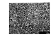
- FIG. 4 is an SEM photograph of the film surface of Example 1
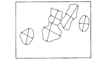
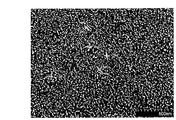
- FIG. 5 is a schematic diagram schematically showing a part of FIG. 6 is an SEM photograph of the film surface of Comparative Example 1
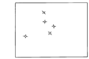
- FIG. 7 is a schematic diagram schematically showing a part of FIG.
- the major axis and minor axis of a plurality of crystals appearing in the SEM photograph were measured.
- the major axis is the length of the longest diameter of each crystal, and the minor axis is a direction that intersects the major axis and is shorter than the major axis.
- Table 8 shows the measurement result of the crystal grain size of Example 1
- Table 9 shows the measurement result of the crystal grain size of Comparative Example 1.
- Example 1 As shown in Table 8 and Table 9, the crystal grain size (average value) in Example 1 was larger than that in Comparative Example 1. Although an example, in Example 1, a crystal grain size 10 times or more larger than that in Comparative Example 1 was obtained.
- the crystal grain size can be controlled in part by the substrate heating temperature during vapor deposition.
- the substrate heating temperature is higher than in Comparative Example 1.
- the dustproof lens of the present invention can obtain high conductivity (low surface resistance) without impairing transparency. Therefore, the dustproof lens of the present invention can obtain excellent dustproof performance while maintaining transparency.
- the dustproof lens of the present invention can obtain an excellent antireflection effect as well as dustproof performance.
- the dustproof lens of the present invention can suppress the adhesion of dust to the lens surface, and can be preferably applied to a glass lens for a surveillance camera, a vehicle-mounted camera, and a projector.
Landscapes
- Physics & Mathematics (AREA)
- Chemical & Material Sciences (AREA)
- Optics & Photonics (AREA)
- General Physics & Mathematics (AREA)
- Materials Engineering (AREA)
- Metallurgy (AREA)
- Organic Chemistry (AREA)
- Mechanical Engineering (AREA)
- Engineering & Computer Science (AREA)
- Chemical Kinetics & Catalysis (AREA)
- Inorganic Chemistry (AREA)
- Surface Treatment Of Optical Elements (AREA)
- Physical Vapour Deposition (AREA)
Abstract
透明性を損なわず、防塵性能を向上させた防塵レンズ及びその製造方法を提供することを目的とする。ガラスレンズの表面に、少なくとも、導電性膜が形成されており、前記導電性膜は、TiO2及びTi3O5の少なくとも一方からなる酸化チタンの単層、或いは、前記酸化チタンを50%以上含む混合層で形成されており、前記導電性膜の膜厚は、1nm以上であり、前記導電性膜の面内方向の結晶粒径は、200nm以上である、ことを特徴とする防塵レンズ。
Description
本発明は、防塵レンズ及びその製造方法に関する。
一般的に、光学ガラスは、抵抗率が高いため帯電しやすい。このため、光学ガラスを用いたレンズの表面には、塵埃が付着しやすいという問題がある。帯電した塵埃は、レンズ表面に付着すると取れにくく、レンズを用いた光学系により形成される像に、悪影響を及ぼす。
下記の特許文献には、基板の表面に、不足当量酸化チタン膜を形成してなる、帯電防止性能を有する光学部材が開示されている。
しかしながら、特許文献1に示すように、酸化チタンを、酸素欠損させると、酸化チタン膜は、メタルに近づく。このため、膜の透過率が低下し透明性が損なわれる問題があった。
本発明は、以上の問題意識に基づいてなされたものであり、透明性を損なわず、防塵性能を向上させた防塵レンズ及びその製造方法を提供することを目的とする。
本発明の防塵レンズは、ガラスレンズの表面に、少なくとも、導電性膜が形成されており、前記導電性膜は、TiO2及びTi3O5の少なくとも一方からなる酸化チタンの単層、或いは、前記酸化チタンを50%以上含む混合層で形成されており、前記導電性膜の膜厚は、1nm以上であり、前記導電性膜の面内方向の結晶粒径は、200nm以上である、ことを特徴とする。
本発明では、前記ガラスレンズの表面に、前記導電性膜の単層膜が形成されていてもよい。
本発明では、前記ガラスレンズの表面に、前記導電性膜を含む反射防止膜が形成されており、前記反射防止膜の最外層は、前記ガラスレンズよりも屈折率の低い低屈折率膜で形成されていることが好ましい。
本発明では、前記ガラスレンズの表面に形成された膜の表面抵抗は、1013(Ω/□)以下であることが好ましい。
本発明の塵埃レンズの製造方法は、ガラスレンズの表面に、少なくとも、導電性膜を形成する工程、を含み、前記導電性膜を形成する工程では、TiO2及びTi3O5の少なくとも一方からなる酸化チタンの単層、或いは、前記酸化チタンを50%以上含む混合層を、1nm以上の膜厚で、面内方向の結晶粒径が200nm以上となるように形成する、ことを特徴とする。
本発明では、前記導電性膜を蒸着法で成膜する際の基板加熱温度を、250℃以上とすることが好ましい。
本発明では、前記導電性膜を成膜する際の酸素ガスを、5.0×10⁻³Pa以上のガス圧にて導入することが好ましい。
本発明によれば、透明性を損なわず、防塵性能を向上させた防塵レンズ及びその製造方法を提供することができる。
以下、本発明を実施するための形態(以下、単に「本実施形態」という。)について詳細に説明する。
従来において、基板表面に成膜される酸化チタン膜を酸素欠損させることで、帯電防止性能を向上させる技術が知られている。しかしながら、酸素欠損は、膜をメタルに近づけることになり、透明性が損なわれ、光学膜として適切に使用することができない。
そこで、このような技術背景の下、本発明者らは、透明性(透過性能)を損なうことなく導電性に優れた膜を開発するに至った。すなわち、本実施形態における防塵ガラスは、以下の特徴的部分を備えている。
(1)ガラスレンズの表面に、少なくとも、導電性膜が形成されている。
(2)導電性膜は、TiO2及びTi3O5の少なくとも一方からなる酸化チタンの単層、或いは、前記酸化チタンを50%以上含む混合層で形成されている。
(3)導電性膜の膜厚は、1nm以上である。
(4)導電性膜の面内方向の結晶粒径は、200nm以上である。
(1)ガラスレンズの表面に、少なくとも、導電性膜が形成されている。
(2)導電性膜は、TiO2及びTi3O5の少なくとも一方からなる酸化チタンの単層、或いは、前記酸化チタンを50%以上含む混合層で形成されている。
(3)導電性膜の膜厚は、1nm以上である。
(4)導電性膜の面内方向の結晶粒径は、200nm以上である。
図1は、本実施形態の防塵レンズの模式図である。図1に示す防塵レンズ1は、基板としてのガラスレンズ2と、ガラスレンズ2の光入射側の表面に形成された導電性膜3と、を有して構成される。
ガラスレンズ2は、特に限定されるものでないが、例えば、監視カメラや車載カメラ用、及び、プロジェクター用のガラスレンズである。また、導電性膜3が成膜されるガラスレンズ2の表面は、例えば、非球面である。図1のガラスレンズ2は、例えば、負のパワーを有するメニスカスレンズであるが、正のパワーを有するメニスカスレンズであってもよいし、両凸レンズあるいは両凹レンズ等でもよい。ただし、ガラスレンズ2の表面は、非球面以外であってもよい。
以下、ガラスレンズ2の表面に形成される導電性膜3及び、反射防止膜4について詳述する。
<第1実施形態>
図2に示す第1実施形態では、ガラスレンズ2の表面に、導電性膜3の単層膜が形成されている。このように、図2では、導電性膜3が、ガラスレンズ2の表面に直接形成され、ガラスレンズ2と導電性膜3のみで構成されている。ただし、導電性膜3とガラスレンズ2と間に、密着性や導電性膜3の結晶性を向上させるための下地層(図示せず)が介在する形態も、第1実施形態に含まれる。
図2に示す第1実施形態では、ガラスレンズ2の表面に、導電性膜3の単層膜が形成されている。このように、図2では、導電性膜3が、ガラスレンズ2の表面に直接形成され、ガラスレンズ2と導電性膜3のみで構成されている。ただし、導電性膜3とガラスレンズ2と間に、密着性や導電性膜3の結晶性を向上させるための下地層(図示せず)が介在する形態も、第1実施形態に含まれる。
上記(2)に記載したように、導電性膜3は、TiO2(二酸化チタン)及びTi3O5(五酸化三チタン)の少なくとも一方からなる酸化チタンの単層、或いは、酸化チタンを50%以上含む混合層で形成されている。
酸化チタンは、TiO2及びTi3O5の化学式で示され、TiO2及びTi3O5は、本実施形態では、化学量論組成として酸素欠損していない酸化チタンと定義される。導電性膜3は、少なくとも、TiO2を含むことが好ましい。Ti3O5は、TiO2を成膜する際の出発材料として用いることができ、Ti3O5全てが、TiO2に入れ替わった状態で成膜されてもよいし(相転移)、膜中にTi3O5の一部が残されていてもよい。酸化チタンの組成分析は、既存の方法を用いることができ、例えば、分光光度計により測定することが可能である。なお、導電性膜3を構成する酸化チタンは、TiO2単相、及び、TiO2とTi3O5との混相のほか、Ti3O5の単相で構成されていてもよい。
また、導電性膜3は、酸化チタンが50%以上100%未満含される混合層であっても、酸化チタンが100%の単層であってもよい。混合層としては、酸化チタン以外の金属酸化物を混ぜたり、或いは、酸化チタン以外に、半導体物質、導電性物質、及び絶縁性物質の少なくともいずれかを混合させることができる。なお、導電性膜3に含まれる酸化チタン以外の材質は、酸化チタンとの混合層において、透明性を保ちつつ、導電性を向上させることが可能な材質であることが必要である。酸化チタン以外の材質としては、SiO2、Ta2O5、Nb2O5、ZrO2、Al2O3、MgF2といった、一般的に蒸着材料として使われる物質が使用可能である。
導電性膜3が混合層で形成される場合、酸化チタンは80%以上含まれていることが好ましい。
なお、本実施形態において、含有量である「%」は、「質量%」である。
上記(3)に記載したように、導電性膜3の膜厚は、1nm以上である。本実施形態において、導電性膜3の膜厚の上限値を限定するものでない。ただし、膜厚の上限値は500nm程度以下であることが好ましい。膜厚は、例えば、縦断面TEM写真(膜厚方向に切断し、その切断面を観察したTEM写真)を用いて測定することができる。なお本実施形態では、導電性膜3の膜厚が上記の範囲となるように制御するが、測定条件等により測定誤差やずれが生じた場合でも、例えば、透明性を保ちつつ、所望の導電性(表面抵抗)を満たすことで、本実施形態の構成を含むものと推測することが可能である。
導電性膜3の膜厚は、結晶粒径の観点から、5nm以上であることが好ましく、10nm以上であることがより好ましく、30nm以上であることが更に好ましい。また、導電性膜3の膜厚は、透明性の観点から、400nm以下であることが好ましく、300nm以下であることがより好ましく、200nm以下であることが更に好ましい。
上記(4)に記載したように、導電性膜3の面内方向の結晶粒径は、200nm以上である。本実施形態において、導電性膜3の結晶粒径の上限値を限定するものでない。ただし、結晶粒径の上限値は、1000nm程度以下であることが好ましい。結晶粒径は、膜表面、或いは、横断面(膜厚方向に対する垂直方向の面)のSEM写真を用いて測定することができる。すなわち、導電性膜3の結晶粒径は、面内方向(膜厚方向に対して直交する方向の面)の結晶粒径として定義される。なお、本実施形態では、導電性膜3の結晶粒径が上記の範囲となるように制御するが、測定条件等により測定誤差やずれが生じた場合でも、例えば、透明性を保ちつつ、所望の導電性(表面抵抗)を満たすことで、本実施形態の構成を含むものと推測することが可能である。
導電性膜3の結晶粒径は、導電性(表面抵抗)の観点から、300nm以上であることが好ましく、400nm以上であることがより好ましい。また、導電性膜3の結晶粒径は、導電性膜3の表面平坦性や機械強度の観点から、900nm以下であることが好ましく、800nm以下であることがより好ましく、700nm以下であることが更に好ましく、600nm以下が最も好ましい。
導電性膜3の表面抵抗は、1013(Ω/□)以下であることが好ましい。表面抵抗は、5×1012(Ω/□)以下であることがより好ましく、5×1011(Ω/□)以下であることが更に好ましく、1011(Ω/□)以下であることが最も好ましい。
<第2実施形態>
図3に示す第2実施形態では、ガラスレンズ2の表面に、導電性膜3を含む反射防止膜4が形成されている。反射防止膜4を構成する各膜は、いずれも透明性に優れた材料である。
図3に示す第2実施形態では、ガラスレンズ2の表面に、導電性膜3を含む反射防止膜4が形成されている。反射防止膜4を構成する各膜は、いずれも透明性に優れた材料である。
反射防止膜4は、例えば、低屈折率膜と高屈折率膜(低屈折率膜よりも屈折率が高い)とを交互に積層した構成とすることができる。このとき、図3に示すように、反射防止膜4の最外層は、ガラスレンズ2よりも屈折率の低い低屈折率膜5で形成される。導電性膜3は、一般的に、ガラスレンズ2の屈折率より高くなるため、導電性膜3は、反射防止膜4の最外層以外に位置する高屈折率膜であることが好ましい。
図3に示す第2実施形態では、反射防止膜4は、ガラスレンズ2側から、低屈折率膜5、高屈折率膜としての導電性膜3及び、最外層としての低屈折率膜5の順に積層されている。図3では、反射防止膜4を3層構造としたが、層数は、一例に過ぎない。よって、反射防止膜4は、導電性膜3と低屈折率膜5の2層構造としてもよいし、4層以上で構成されてもよい。このとき、高屈折率膜の少なくとも一層に、本実施形態の導電性膜3を用いればよいが、全ての高屈折率膜が、本実施形態の導電性膜3であることが好ましい。すなわち、例えば、反射防止膜4は、低屈折率膜5/導電性膜3/低屈折率膜5/導電性膜3/・・・低屈折率膜5の積層構造で形成される。
なお、反射防止膜4の層数の上限を限定するものでないが、例えば、15層程度以下、好ましくは、10層程度以下である。反射防止膜4の積層数や、材質は、反射率を抑制する波長領域に基づいて種々選択できる。
本実施形態では、反射防止膜4を構成する低屈折率膜5の材質を限定するものでないが、例えば、低屈折率膜5は、SiO2、Al2O3、及びMgF2から選択される単層膜又は2種以上を含む混合膜で形成される。
反射防止膜4の膜厚を限定するものでないが、反射防止膜4の膜厚(トータル厚)は、50nm~500nm程度である。
第2実施形態における1層あるいは2層以上の導電性膜3は、夫々、上記に挙げた(2)~(4)の特徴を全て備えている。なお、上記のように、第2実施形態における反射防止膜4の膜厚は、50nm~500nm程度であることが好ましいので、この範囲に収まるように、各導電性膜3の膜厚は調節される。導電性膜3の積層数が多くなるほど、導電性膜3の各膜厚の上限値は、より低い値にて調節される。例えば、第2実施形態では、導電性膜3の層数が4層程度以下であるとき、各導電性膜3の膜厚は、10nm~100nm程度であることが好ましい。
第2実施形態における反射防止膜4の表面抵抗は、1013(Ω/□)以下であることが好ましい。表面抵抗は、5×1012(Ω/□)以下であることがより好ましく、5×1011(Ω/□)以下であることが更に好ましく、1011(Ω/□)以下であることが最も好ましい。
上記したように、第1実施形態及び第2実施形態では、導電性膜3の材質、膜厚及び結晶粒径を夫々規定する。
結晶粒径と抵抗率との関係について考察する。結晶粒径が大きくなると、単位体積当たりに占める結晶粒界の数は少なくなる。結晶粒界は、電子移動を阻害する要因になるため、結晶粒界が少なくなることで、電子移動が起こりやすくなる。また、電子は、結晶粒界に沿って流れる。結晶粒径が大きくなると、単位体積当たりに占める結晶粒界の数は少なくなり、その結果、単位体積当たりに占める結晶粒界のトータル長さは短くなる。このため、結晶粒径が大きいほど電子の流れる距離を短くできる。以上により、結晶粒径が大きくなると、抵抗率は低下するものと考えられる。よって、結晶粒径を大きくすることで、導電性を高めることができる。
また、本実施形態では、導電性膜3に使用される酸化チタンは、TiO2及びTi3O5であり、酸素欠損が生じていない。このため、膜の透明性が損なわれない。また、導電性膜3の膜厚は、適度に薄く形成されており、結晶粒径の成長促進とともに、透明性を適切に、保つことができる。
以上により、第1実施形態及び第2実施形態における防塵レンズ1は、透明性を損なわず、優れた導電性を得ることができ、防塵性能を効果的に向上させることができる。また、第2実施形態では、防塵性能とともに、優れた反射防止効果を得ることができる。
<防塵レンズの製造方法>
図2に示す第1実施形態の防塵レンズの製造方法について説明する。図2に示す防塵レンズ1では、ガラスレンズ2の表面に、導電性膜3を成膜する。このとき、導電性膜3を、TiO2及びTi3O5の少なくとも一方からなる酸化チタンの単層、或いは、前記酸化チタンを50%以上含む混合層にて、1nm以上の膜厚で成膜する。また、この際、導電性膜3の面内方向の結晶粒径が200nm以上となるように形成する。
図2に示す第1実施形態の防塵レンズの製造方法について説明する。図2に示す防塵レンズ1では、ガラスレンズ2の表面に、導電性膜3を成膜する。このとき、導電性膜3を、TiO2及びTi3O5の少なくとも一方からなる酸化チタンの単層、或いは、前記酸化チタンを50%以上含む混合層にて、1nm以上の膜厚で成膜する。また、この際、導電性膜3の面内方向の結晶粒径が200nm以上となるように形成する。
成膜方法を限定するものではないが、例えば、導電性膜3を、イオンビームアシスト蒸着(Ion-beam Assisted Deposition:IAD)法、或いは、電子ビーム(Electron Beam:EB)法により成膜することができる。イオンビームアシスト蒸着法では、真空蒸着中に、イオン銃で、ガスイオンを基板であるガラスレンズの表面に照射する。また、電子ビーム法では、高真空雰囲気の中で、蒸発材料をるつぼに入れ、電子ビームをるつぼに照射し、るつぼ中の蒸発材料を加熱蒸発させる。
例えば、本実施形態では、蒸着材料としてTi3O5を用い、成膜チャンバ内にて減圧下で、Ti3O5を加熱蒸発させる。蒸発したTi3O5は、基板としてのガラスレンズ2の表面に向かう。このとき、O2と結合し、Ti3O5は、TiO2となってガラスレンズ2の表面に堆積する。したがって、蒸着法を用いて導電性膜3を成膜する場合、導電性膜3は、TiO2単相か、或いは、TiO2とTi3O5との混相となりやすい。
また、本実施形態では、導電性膜3を蒸着法で成膜する際、成膜チャンバ内での基板加熱温度を、250℃以上とすることが好ましい。また、基板加熱温度の上限値を限定するものでないが、例えば、400℃以下に調節することができる。
また、導電性膜を成膜する際の酸素ガスを、5.0×10⁻³Pa以上のガス圧にて導入することが好ましい。また、酸素ガスのガス圧を、1.0×10⁻²Pa~3.0×10⁻²Pa程度にて調節することがより好ましい。
このように、基板加熱温度及び酸素ガスのガス圧を調節することで、導電性膜3の面内方向の結晶粒径が200nm以上となるように適切に、制御することができる。
図3に示す第2実施形態の防塵レンズの製造方法では、ガラスレンズ2の表面に、反射防止膜4を成膜する。このとき、成膜チャンバ内での基板加熱温度を上記のように250℃以上の減圧下で保持したまま、低屈折率膜5及び導電性膜3を順に蒸着法にて成膜する。このとき、反射防止膜4の最外層が低屈折率膜5となるように積層順や積層数を調節する。
低屈折率膜5及び導電性膜3を蒸着法で成膜する場合、イオンビームアシスト蒸着法を用いることが、各膜間の密着性を高めることができ好ましいが、低屈折率膜5としてMgF2を用いる場合、イオンビームアシスト蒸着法を使用できない。したがって、例えば、最外層としてMgF2を用い、それ以外の低屈折率膜5にはSiO2等の酸化膜を用いる場合は、最外層を除く低屈折率膜5及び導電性膜3を、イオンビームアシスト蒸着法で成膜する。そして、最外層のMgF2を電子ビーム法で成膜する。このように、成膜する材質等に応じて、反射防止膜4を2種以上の成膜方法で成膜することができる。
本実施形態における防塵レンズ1の製造方法では、TiO2及びTi3O5の少なくとも一方からなる酸化チタンの単層、或いは、酸化チタンを50%以上含む混合層であり、1nm以上の膜厚を有し、200nm以上の面内方向の結晶粒径を有する導電性膜3を、簡単且つ適切に成膜することができる。このように、従来と異なり、酸化チタンを酸素欠損させずに成膜するため、導電性膜3の透明性を保つことができる。また、導電性膜3を成膜した際、酸化チタンの結晶粒径を200nm以上に大きくできるため、抵抗率を減少させることができる。この結果、導電性膜3の導電性を高めることができ、帯電しにくい膜とすることができる。よって、本実施形態の導電性膜3をガラスレンズ2の表面に有することで、塵埃が付着しにくい防塵ガラスを製造することができる。
また、第2実施形態では、導電性膜を用いた反射防止膜を成膜することができる。すなわち、反射防止機能を兼ね備えた防塵レンズを製造することが可能である。
なお、上記した防塵レンズの製造方法では、導電性膜3を、蒸着法にて成膜したが、スパッタ法で成膜することもできる。
なお、上記した防塵レンズの製造方法では、導電性膜3を、蒸着法にて成膜したが、スパッタ法で成膜することもできる。
以下、本実施形態を実施例及び比較例を用いてより具体的に説明する。実験では、以下に示す実施例1から実施例6及び比較例1を製造した。
[実施例1]
実施例1では、以下の表1に示す材料を用い、表1に示す基板加熱温度にて、反射防止膜を成膜し、表1に示す膜厚及び屈折率を有する防塵レンズを得た。なお、ガラスレンズの屈折率nd(d線(588nm)での屈折率)は、1.85135であった。ガラスレンズの屈折率ndは、実施例2から実施例6及び比較例1においても同様である。ここで、各層の屈折率は、膜の反射率から換算して求めた(大気中の膜の屈折率に該当)。具体的には、大気中に取り出した基板を、オリンパス(株)製の顕微鏡型分光測定機(USPM―RU3)にて反射率を測定し、屈折率に換算して求めた。なお、屈折率は、波長550nmにおけるものである。また、膜厚は、例えば、断面TEM写真を用いて測定することができる。上記の屈折率、及び膜厚の測定は、実施例2から実施例6及び比較例1においても同様である。
実施例1では、以下の表1に示す材料を用い、表1に示す基板加熱温度にて、反射防止膜を成膜し、表1に示す膜厚及び屈折率を有する防塵レンズを得た。なお、ガラスレンズの屈折率nd(d線(588nm)での屈折率)は、1.85135であった。ガラスレンズの屈折率ndは、実施例2から実施例6及び比較例1においても同様である。ここで、各層の屈折率は、膜の反射率から換算して求めた(大気中の膜の屈折率に該当)。具体的には、大気中に取り出した基板を、オリンパス(株)製の顕微鏡型分光測定機(USPM―RU3)にて反射率を測定し、屈折率に換算して求めた。なお、屈折率は、波長550nmにおけるものである。また、膜厚は、例えば、断面TEM写真を用いて測定することができる。上記の屈折率、及び膜厚の測定は、実施例2から実施例6及び比較例1においても同様である。

実施例1では、基板加熱温度を350℃とし、SiO2と導電性膜とを、イオンアシストビーム蒸着法にて、交互に6層まで積層した。導電性膜は、Ti3O5を出発原料として蒸着され、このとき、Ti3O5の全部又は一部が、TiO2に入れ替わって成膜されやすい。導電性膜の膜構造は、分光光度計により測定することができる。本実施例では、導電性膜は、TiO2単相、Ti3O5単相、或いは、TiO2及びTi3O5の混相のいずれかの膜構造であればよい。
また、導電性膜の成膜の際の、酸素ガスのガス圧を、2.0×10⁻²Pa程度とした。このガス圧は、実施例2から実施例6及び、比較例1において同様である。
また、実施例1では、反射防止膜の最外層として、電子ビーム法にて、MgF2を成膜した。
[実施例2]
実施例2では、以下の表2に示す材料を用い、表2に示す基板加熱温度にて、反射防止膜を成膜し、表2に示す膜厚及び屈折率を有する防塵レンズを得た。
実施例2では、以下の表2に示す材料を用い、表2に示す基板加熱温度にて、反射防止膜を成膜し、表2に示す膜厚及び屈折率を有する防塵レンズを得た。
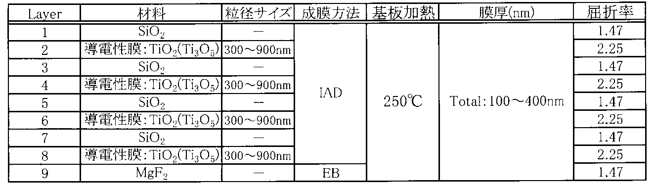
実施例2では、基板加熱温度を250℃とし、SiO2と導電性膜とを、イオンアシストビーム蒸着法にて、交互に8層まで積層した。また、実施例2では、反射防止膜の最外層として、MgF2を、電子ビーム法にて、成膜した。
[実施例3]
実施例3では、以下の表3に示す材料を用い、表3に示す基板加熱温度にて、導電性膜を成膜し、表3に示す膜厚及び屈折率を有する防塵レンズを得た。
実施例3では、以下の表3に示す材料を用い、表3に示す基板加熱温度にて、導電性膜を成膜し、表3に示す膜厚及び屈折率を有する防塵レンズを得た。

実施例3では、基板加熱温度を350℃とし、ガラスレンズの表面に、導電性膜を一層のみ成膜した。
[実施例4]
実施例4では、以下の表4に示す材料を用い、表4に示す基板加熱温度にて、反射防止膜を成膜し、表4に示す膜厚及び屈折率を有する防塵レンズを得た。
実施例4では、以下の表4に示す材料を用い、表4に示す基板加熱温度にて、反射防止膜を成膜し、表4に示す膜厚及び屈折率を有する防塵レンズを得た。

実施例4では、基板加熱温度を350℃とし、MgF2と導電性膜とを、電子ビーム法にて、交互に7層まで積層した。
[実施例5]
実施例5では、以下の表5に示す材料を用い、表5に示す基板加熱温度にて、反射防止膜を成膜し、表5に示す膜厚及び屈折率を有する防塵レンズを得た。
実施例5では、以下の表5に示す材料を用い、表5に示す基板加熱温度にて、反射防止膜を成膜し、表5に示す膜厚及び屈折率を有する防塵レンズを得た。

実施例5では、基板加熱温度を350℃とし、Al2O3と導電性膜とを、イオンアシストビーム蒸着法にて、交互に6層まで積層した。また、実施例5では、反射防止膜の最外層として、MgF2を、電子ビーム法にて、成膜した。
[実施例6]
実施例6では、以下の表6に示す材料を用いて、反射防止膜を成膜し、表6に示す膜厚及び屈折率を有する防塵レンズを得た。
実施例6では、以下の表6に示す材料を用いて、反射防止膜を成膜し、表6に示す膜厚及び屈折率を有する防塵レンズを得た。
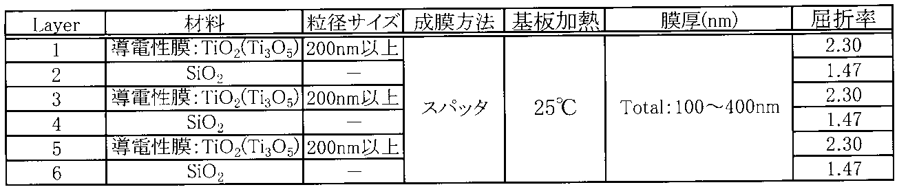
実施例6では、基板加熱温度を25℃(無加熱)とし、スパッタ法にて、SiO2と導電性膜とを、交互に6層まで積層した。
[比較例1]
比較例1では、以下の表7に示す材料を用い、表7に示す基板加熱温度にて、反射防止膜を成膜し、表7に示す膜厚及び屈折率を有する防塵レンズを得た。
比較例1では、以下の表7に示す材料を用い、表7に示す基板加熱温度にて、反射防止膜を成膜し、表7に示す膜厚及び屈折率を有する防塵レンズを得た。

比較例1では、基板加熱温度を200℃とし、SiO2と導電性膜とを、電子ビーム法にて、交互に7層まで積層した。
[表面抵抗の測定]
各実施例及び比較例の各膜の表面抵抗を、三菱化学製ハイレスタ-UXを用いて測定した。
各実施例及び比較例の各膜の表面抵抗を、三菱化学製ハイレスタ-UXを用いて測定した。
[表面抵抗の測定結果]
実施例1の表面抵抗は、3.84×10¹⁰(Ω/□)、実施例2の表面抵抗は、2.00×1010(Ω/□)、実施例3の表面抵抗は、1.80×1010(Ω/□)、実施例4の表面抵抗は、4.00×1010(Ω/□)、実施例5の表面抵抗は、5.00×1011(Ω/□)、実施例6の表面抵抗は、3.50×1012(Ω/□)、比較例1の表面抵抗は、5.00×1014(Ω/□)であった。
実施例1の表面抵抗は、3.84×10¹⁰(Ω/□)、実施例2の表面抵抗は、2.00×1010(Ω/□)、実施例3の表面抵抗は、1.80×1010(Ω/□)、実施例4の表面抵抗は、4.00×1010(Ω/□)、実施例5の表面抵抗は、5.00×1011(Ω/□)、実施例6の表面抵抗は、3.50×1012(Ω/□)、比較例1の表面抵抗は、5.00×1014(Ω/□)であった。
この実験結果から、各実施例は、比較例に比べて、表面抵抗を小さくできることがわかった。
実験結果に基づいて、本実施例の表面抵抗は、1013(Ω/□)以下が好ましい範囲であると規定した。なお、表面抵抗は、5×1012(Ω/□)以下がより好ましく、5×1011(Ω/□)以下が更に好ましく、1011(Ω/□)以下が最も好ましい範囲と規定した。
また、実施例3のように、レンズ表面に、導電性膜を単層膜で形成することで、効果的に、表面抵抗を小さくすることができるとわかった。
また、導電性膜と低屈折率膜とを交互に積層した反射防止膜を、レンズ表面に成膜した形態において、積層数、材質、及び成膜方法を変えても、低い表面抵抗を得ることができるとわかった。
[実施例1と比較例1との結晶粒径の測定]
図4は、実施例1の膜表面のSEM写真であり、図5は、図4の一部分を模式的に示した模式図である。図6は、比較例1の膜表面のSEM写真であり、図7は、図6の一部分を模式的に示した模式図である。
図4は、実施例1の膜表面のSEM写真であり、図5は、図4の一部分を模式的に示した模式図である。図6は、比較例1の膜表面のSEM写真であり、図7は、図6の一部分を模式的に示した模式図である。
図4、図6に示すように、SEM写真に現れる、複数の結晶の長径と短径とを測定した。長径は、各結晶の最も長い径の長さであり、短径は、長径に対して交差する方向であって、長径よりも短い側の径である。
表8は、実施例1の結晶粒径の測定結果を示し、表9は、比較例1の結晶粒径の測定結果を示す。
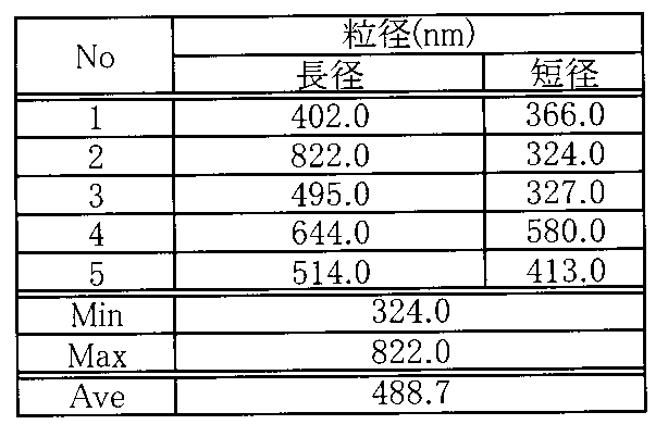

表8及び表9に示すように、結晶粒径(平均値)は、実施例1のほうが比較例1よりも大きくなった。一例ではあるが、実施例1では、比較例1に比べて、10倍以上の大きい結晶粒径が得られた。
結晶粒径の大きさは、一つには、蒸着の際の基板加熱温度により制御できると考えられる。実施例1では、比較例1よりも基板加熱温度が高い。本実施例では、実験結果に基づいて、導電性膜を蒸着法で成膜する際の基板加熱温度を、250℃以上に制御することが好ましいとした。
本発明の防塵レンズは、透明性を損なうことなく、高い導電性(低い表面抵抗)を得ることができる。したがって、本発明の防塵レンズは、透明性を保持しつつ、優れた防塵性能を得ることができる。
また、本発明の防塵レンズは、防塵性能とともに、優れた反射防止効果を得ることもできる。
したがって、本発明の防塵レンズは、レンズ表面への塵埃の付着を抑制することができ、監視カメラや車載カメラ用、及びプロジェクター用のガラスレンズに好ましく適用することができる。
本出願は、2017年5月12日出願の特願2017-095212に基づく。この内容は全てここに含めておく。
Claims (7)
- ガラスレンズの表面に、少なくとも、導電性膜が形成されており、
前記導電性膜は、TiO2及びTi3O5の少なくとも一方からなる酸化チタンの単層、或いは、前記酸化チタンを50%以上含む混合層で形成されており、
前記導電性膜の膜厚は、1nm以上であり、
前記導電性膜の面内方向の結晶粒径は、200nm以上である、
ことを特徴とする防塵レンズ。 - 前記ガラスレンズの表面に、前記導電性膜の単層膜が形成されていることを特徴とする請求項1に記載の防塵レンズ。
- 前記ガラスレンズの表面に、前記導電性膜を含む反射防止膜が形成されており、
前記反射防止膜の最外層は、前記ガラスレンズよりも屈折率の低い低屈折率膜で形成されていることを特徴とする請求項1に記載の防塵レンズ。 - 前記ガラスレンズの表面に形成された膜の表面抵抗は、1013(Ω/□)以下であることを特徴とする請求項1から請求項3のいずれかに記載の防塵レンズ。
- ガラスレンズの表面に、少なくとも、導電性膜を形成する工程、を含み、
前記導電性膜を形成する工程では、TiO2及びTi3O5の少なくとも一方からなる酸化チタンの単層、或いは、前記酸化チタンを50%以上含む混合層を、1nm以上の膜厚で、面内方向の結晶粒径が200nm以上となるように形成する、
ことを特徴とする防塵レンズの製造方法。 - 前記導電性膜を蒸着法で成膜する際の基板加熱温度を、250℃以上とすることを特徴とする請求項5に記載の防塵レンズの製造方法。
- 前記導電性膜を成膜する際の酸素ガスを、5.0×10⁻³Pa以上のガス圧にて導入することを特徴とする請求項5又は請求項6に記載の防塵レンズの製造方法。
Priority Applications (1)
| Application Number | Priority Date | Filing Date | Title |
|---|---|---|---|
| CN201880031151.XA CN110869818B (zh) | 2017-05-12 | 2018-04-27 | 防尘透镜及其制造方法 |
Applications Claiming Priority (2)
| Application Number | Priority Date | Filing Date | Title |
|---|---|---|---|
| JP2017095212A JP7117081B2 (ja) | 2017-05-12 | 2017-05-12 | 防塵レンズ及びその製造方法 |
| JP2017-095212 | 2017-05-12 |
Publications (1)
| Publication Number | Publication Date |
|---|---|
| WO2018207652A1 true WO2018207652A1 (ja) | 2018-11-15 |
Family
ID=64105293
Family Applications (1)
| Application Number | Title | Priority Date | Filing Date |
|---|---|---|---|
| PCT/JP2018/017119 Ceased WO2018207652A1 (ja) | 2017-05-12 | 2018-04-27 | 防塵レンズ及びその製造方法 |
Country Status (3)
| Country | Link |
|---|---|
| JP (1) | JP7117081B2 (ja) |
| CN (1) | CN110869818B (ja) |
| WO (1) | WO2018207652A1 (ja) |
Families Citing this family (1)
| Publication number | Priority date | Publication date | Assignee | Title |
|---|---|---|---|---|
| WO2021131316A1 (ja) * | 2019-12-25 | 2021-07-01 | コニカミノルタ株式会社 | 反射防止膜付き光学レンズの製造方法 |
Citations (4)
| Publication number | Priority date | Publication date | Assignee | Title |
|---|---|---|---|---|
| JP2008084824A (ja) * | 2006-03-20 | 2008-04-10 | Kanagawa Acad Of Sci & Technol | 導電体の製造方法 |
| WO2009028569A1 (ja) * | 2007-08-29 | 2009-03-05 | Asahi Glass Company, Limited | 導電体層の製造方法 |
| JP2010529290A (ja) * | 2007-06-01 | 2010-08-26 | フラウンホッファー−ゲゼルシャフト・ツァー・フォデラング・デル・アンゲワンテン・フォーシュング・エー.ファウ. | 高光触媒活性を有する酸化チタン層の製造方法およびこの方法により製造された酸化チタン層 |
| JP2011039218A (ja) * | 2009-08-10 | 2011-02-24 | Seiko Epson Corp | 光学物品の製造方法 |
Family Cites Families (6)
| Publication number | Priority date | Publication date | Assignee | Title |
|---|---|---|---|---|
| CN101066011A (zh) * | 2004-11-30 | 2007-10-31 | 旭硝子株式会社 | 导电性层积体、等离子显示器用的电磁波屏蔽膜及保护板 |
| JP2011100111A (ja) | 2009-10-09 | 2011-05-19 | Seiko Epson Corp | 光学物品、光学物品の製造方法、電子機器 |
| KR20150126885A (ko) * | 2013-03-01 | 2015-11-13 | 블라디미르 클렙신 | 반사 방지 코팅 |
| JP6313941B2 (ja) * | 2013-08-30 | 2018-04-18 | Hoya株式会社 | 眼鏡レンズ |
| CN103848623B (zh) * | 2014-02-20 | 2017-01-04 | 福建阿石创新材料股份有限公司 | 一种高折射率导电薄膜材料钛氧化物及其制备方法 |
| CN205263336U (zh) * | 2016-02-26 | 2016-05-25 | 视悦光学有限公司 | 一种超薄防雾非球面复合眼镜片 |
-
2017
- 2017-05-12 JP JP2017095212A patent/JP7117081B2/ja active Active
-
2018
- 2018-04-27 WO PCT/JP2018/017119 patent/WO2018207652A1/ja not_active Ceased
- 2018-04-27 CN CN201880031151.XA patent/CN110869818B/zh active Active
Patent Citations (4)
| Publication number | Priority date | Publication date | Assignee | Title |
|---|---|---|---|---|
| JP2008084824A (ja) * | 2006-03-20 | 2008-04-10 | Kanagawa Acad Of Sci & Technol | 導電体の製造方法 |
| JP2010529290A (ja) * | 2007-06-01 | 2010-08-26 | フラウンホッファー−ゲゼルシャフト・ツァー・フォデラング・デル・アンゲワンテン・フォーシュング・エー.ファウ. | 高光触媒活性を有する酸化チタン層の製造方法およびこの方法により製造された酸化チタン層 |
| WO2009028569A1 (ja) * | 2007-08-29 | 2009-03-05 | Asahi Glass Company, Limited | 導電体層の製造方法 |
| JP2011039218A (ja) * | 2009-08-10 | 2011-02-24 | Seiko Epson Corp | 光学物品の製造方法 |
Also Published As
| Publication number | Publication date |
|---|---|
| JP7117081B2 (ja) | 2022-08-12 |
| CN110869818B (zh) | 2024-03-15 |
| CN110869818A (zh) | 2020-03-06 |
| JP2018194569A (ja) | 2018-12-06 |
Similar Documents
| Publication | Publication Date | Title |
|---|---|---|
| JP4178190B2 (ja) | 多層膜を有する光学素子およびその製造方法 | |
| JP6656389B2 (ja) | 反射防止膜、反射防止膜の製造方法、光学素子および光学系 | |
| CN113031122B (zh) | 带防反射膜的光学透镜、投影透镜以及投影透镜光学系统 | |
| JP7216471B2 (ja) | 車載レンズ用のプラスチックレンズ及びその製造方法 | |
| JP5549342B2 (ja) | 反射防止膜、及びこれを有する光学部材 | |
| CN110869818B (zh) | 防尘透镜及其制造方法 | |
| JP6989289B2 (ja) | 親水性反射防止膜付きレンズ及びその製造方法 | |
| CN104321670A (zh) | 光学元件 | |
| JP7493918B2 (ja) | 反射防止膜付き光学部材及びその製造方法 | |
| JP3243474B2 (ja) | 多層膜バンドパスフィルタの製造方法及び波長シフト温度係数値が略ゼロの多層膜バンドパスフィルタ | |
| JP2003043202A (ja) | 反射防止膜及び光学部品 | |
| JP4804830B2 (ja) | 多層膜の成膜方法および成膜装置 | |
| JP5084603B2 (ja) | 偏光子及び液晶プロジェクタ | |
| JPS6222121B2 (ja) | ||
| JP2010271404A (ja) | 反射防止膜 | |
| JPH11337733A (ja) | 複屈折板及びその作製方法 | |
| JP2000171607A (ja) | 高緻密な多層薄膜およびその成膜方法 | |
| JPH10268107A (ja) | 反射防止膜付合成樹脂レンズ | |
| US3421811A (en) | Coated optical devices | |
| US7760432B2 (en) | Photochromic resistant materials for optical devices in plasma environments | |
| JP2013109004A (ja) | 光学フィルタおよびその製造方法 | |
| JPH11326634A (ja) | 光学多層薄膜および光学多層薄膜の製造方法 | |
| JP2815951B2 (ja) | 反射防止膜 | |
| JP2003073818A (ja) | フッ化物スパッタリングターゲット及びその製造方法 | |
| JP2006030530A (ja) | 光学デバイスおよびその製造方法 |
Legal Events
| Date | Code | Title | Description |
|---|---|---|---|
| 121 | Ep: the epo has been informed by wipo that ep was designated in this application |
Ref document number: 18798217 Country of ref document: EP Kind code of ref document: A1 |
|
| NENP | Non-entry into the national phase |
Ref country code: DE |
|
| 122 | Ep: pct application non-entry in european phase |
Ref document number: 18798217 Country of ref document: EP Kind code of ref document: A1 |