WO2018207408A1 - 半導体封止成形用仮保護フィルム - Google Patents
半導体封止成形用仮保護フィルム Download PDFInfo
- Publication number
- WO2018207408A1 WO2018207408A1 PCT/JP2018/002313 JP2018002313W WO2018207408A1 WO 2018207408 A1 WO2018207408 A1 WO 2018207408A1 JP 2018002313 W JP2018002313 W JP 2018002313W WO 2018207408 A1 WO2018207408 A1 WO 2018207408A1
- Authority
- WO
- WIPO (PCT)
- Prior art keywords
- protective film
- temporary protective
- lead frame
- adhesive layer
- sealing
- Prior art date
- Legal status (The legal status is an assumption and is not a legal conclusion. Google has not performed a legal analysis and makes no representation as to the accuracy of the status listed.)
- Ceased
Links
Images


Classifications
-
- H—ELECTRICITY
- H10—SEMICONDUCTOR DEVICES; ELECTRIC SOLID-STATE DEVICES NOT OTHERWISE PROVIDED FOR
- H10W—GENERIC PACKAGES, INTERCONNECTIONS, CONNECTORS OR OTHER CONSTRUCTIONAL DETAILS OF DEVICES COVERED BY CLASS H10
- H10W74/00—Encapsulations, e.g. protective coatings
- H10W74/01—Manufacture or treatment
- H10W74/019—Manufacture or treatment using temporary auxiliary substrates
-
- H—ELECTRICITY
- H10—SEMICONDUCTOR DEVICES; ELECTRIC SOLID-STATE DEVICES NOT OTHERWISE PROVIDED FOR
- H10W—GENERIC PACKAGES, INTERCONNECTIONS, CONNECTORS OR OTHER CONSTRUCTIONAL DETAILS OF DEVICES COVERED BY CLASS H10
- H10W74/00—Encapsulations, e.g. protective coatings
- H10W74/40—Encapsulations, e.g. protective coatings characterised by their materials
- H10W74/47—Encapsulations, e.g. protective coatings characterised by their materials comprising organic materials, e.g. plastics or resins
-
- B—PERFORMING OPERATIONS; TRANSPORTING
- B32—LAYERED PRODUCTS
- B32B—LAYERED PRODUCTS, i.e. PRODUCTS BUILT-UP OF STRATA OF FLAT OR NON-FLAT, e.g. CELLULAR OR HONEYCOMB, FORM
- B32B25/00—Layered products comprising a layer of natural or synthetic rubber
- B32B25/04—Layered products comprising a layer of natural or synthetic rubber comprising rubber as the main or only constituent of a layer, which is next to another layer of the same or of a different material
- B32B25/08—Layered products comprising a layer of natural or synthetic rubber comprising rubber as the main or only constituent of a layer, which is next to another layer of the same or of a different material of synthetic resin
-
- B—PERFORMING OPERATIONS; TRANSPORTING
- B32—LAYERED PRODUCTS
- B32B—LAYERED PRODUCTS, i.e. PRODUCTS BUILT-UP OF STRATA OF FLAT OR NON-FLAT, e.g. CELLULAR OR HONEYCOMB, FORM
- B32B27/00—Layered products comprising a layer of synthetic resin
-
- B—PERFORMING OPERATIONS; TRANSPORTING
- B32—LAYERED PRODUCTS
- B32B—LAYERED PRODUCTS, i.e. PRODUCTS BUILT-UP OF STRATA OF FLAT OR NON-FLAT, e.g. CELLULAR OR HONEYCOMB, FORM
- B32B27/00—Layered products comprising a layer of synthetic resin
- B32B27/30—Layered products comprising a layer of synthetic resin comprising vinyl (co)polymers; comprising acrylic (co)polymers
-
- B—PERFORMING OPERATIONS; TRANSPORTING
- B32—LAYERED PRODUCTS
- B32B—LAYERED PRODUCTS, i.e. PRODUCTS BUILT-UP OF STRATA OF FLAT OR NON-FLAT, e.g. CELLULAR OR HONEYCOMB, FORM
- B32B27/00—Layered products comprising a layer of synthetic resin
- B32B27/34—Layered products comprising a layer of synthetic resin comprising polyamides
-
- B—PERFORMING OPERATIONS; TRANSPORTING
- B32—LAYERED PRODUCTS
- B32B—LAYERED PRODUCTS, i.e. PRODUCTS BUILT-UP OF STRATA OF FLAT OR NON-FLAT, e.g. CELLULAR OR HONEYCOMB, FORM
- B32B7/00—Layered products characterised by the relation between layers; Layered products characterised by the relative orientation of features between layers, or by the relative values of a measurable parameter between layers, i.e. products comprising layers having different physical, chemical or physicochemical properties; Layered products characterised by the interconnection of layers
- B32B7/02—Physical, chemical or physicochemical properties
-
- B—PERFORMING OPERATIONS; TRANSPORTING
- B32—LAYERED PRODUCTS
- B32B—LAYERED PRODUCTS, i.e. PRODUCTS BUILT-UP OF STRATA OF FLAT OR NON-FLAT, e.g. CELLULAR OR HONEYCOMB, FORM
- B32B7/00—Layered products characterised by the relation between layers; Layered products characterised by the relative orientation of features between layers, or by the relative values of a measurable parameter between layers, i.e. products comprising layers having different physical, chemical or physicochemical properties; Layered products characterised by the interconnection of layers
- B32B7/04—Interconnection of layers
- B32B7/12—Interconnection of layers using interposed adhesives or interposed materials with bonding properties
-
- C—CHEMISTRY; METALLURGY
- C09—DYES; PAINTS; POLISHES; NATURAL RESINS; ADHESIVES; COMPOSITIONS NOT OTHERWISE PROVIDED FOR; APPLICATIONS OF MATERIALS NOT OTHERWISE PROVIDED FOR
- C09J—ADHESIVES; NON-MECHANICAL ASPECTS OF ADHESIVE PROCESSES IN GENERAL; ADHESIVE PROCESSES NOT PROVIDED FOR ELSEWHERE; USE OF MATERIALS AS ADHESIVES
- C09J133/00—Adhesives based on homopolymers or copolymers of compounds having one or more unsaturated aliphatic radicals, each having only one carbon-to-carbon double bond, and at least one being terminated by only one carboxyl radical, or of salts, anhydrides, esters, amides, imides, or nitriles thereof; Adhesives based on derivatives of such polymers
-
- C—CHEMISTRY; METALLURGY
- C09—DYES; PAINTS; POLISHES; NATURAL RESINS; ADHESIVES; COMPOSITIONS NOT OTHERWISE PROVIDED FOR; APPLICATIONS OF MATERIALS NOT OTHERWISE PROVIDED FOR
- C09J—ADHESIVES; NON-MECHANICAL ASPECTS OF ADHESIVE PROCESSES IN GENERAL; ADHESIVE PROCESSES NOT PROVIDED FOR ELSEWHERE; USE OF MATERIALS AS ADHESIVES
- C09J7/00—Adhesives in the form of films or foils
- C09J7/20—Adhesives in the form of films or foils characterised by their carriers
-
- H—ELECTRICITY
- H10—SEMICONDUCTOR DEVICES; ELECTRIC SOLID-STATE DEVICES NOT OTHERWISE PROVIDED FOR
- H10W—GENERIC PACKAGES, INTERCONNECTIONS, CONNECTORS OR OTHER CONSTRUCTIONAL DETAILS OF DEVICES COVERED BY CLASS H10
- H10W70/00—Package substrates; Interposers; Redistribution layers [RDL]
- H10W70/40—Leadframes
- H10W70/479—Leadframes on or in insulating or insulated package substrates, interposers, or redistribution layers
-
- H—ELECTRICITY
- H10—SEMICONDUCTOR DEVICES; ELECTRIC SOLID-STATE DEVICES NOT OTHERWISE PROVIDED FOR
- H10W—GENERIC PACKAGES, INTERCONNECTIONS, CONNECTORS OR OTHER CONSTRUCTIONAL DETAILS OF DEVICES COVERED BY CLASS H10
- H10W72/00—Interconnections or connectors in packages
- H10W72/01—Manufacture or treatment
- H10W72/0198—Manufacture or treatment batch processes
-
- H—ELECTRICITY
- H10—SEMICONDUCTOR DEVICES; ELECTRIC SOLID-STATE DEVICES NOT OTHERWISE PROVIDED FOR
- H10W—GENERIC PACKAGES, INTERCONNECTIONS, CONNECTORS OR OTHER CONSTRUCTIONAL DETAILS OF DEVICES COVERED BY CLASS H10
- H10W72/00—Interconnections or connectors in packages
- H10W72/071—Connecting or disconnecting
- H10W72/073—Connecting or disconnecting of die-attach connectors
-
- H—ELECTRICITY
- H10—SEMICONDUCTOR DEVICES; ELECTRIC SOLID-STATE DEVICES NOT OTHERWISE PROVIDED FOR
- H10W—GENERIC PACKAGES, INTERCONNECTIONS, CONNECTORS OR OTHER CONSTRUCTIONAL DETAILS OF DEVICES COVERED BY CLASS H10
- H10W72/00—Interconnections or connectors in packages
- H10W72/071—Connecting or disconnecting
- H10W72/075—Connecting or disconnecting of bond wires
-
- H—ELECTRICITY
- H10—SEMICONDUCTOR DEVICES; ELECTRIC SOLID-STATE DEVICES NOT OTHERWISE PROVIDED FOR
- H10W—GENERIC PACKAGES, INTERCONNECTIONS, CONNECTORS OR OTHER CONSTRUCTIONAL DETAILS OF DEVICES COVERED BY CLASS H10
- H10W72/00—Interconnections or connectors in packages
- H10W72/30—Die-attach connectors
-
- H—ELECTRICITY
- H10—SEMICONDUCTOR DEVICES; ELECTRIC SOLID-STATE DEVICES NOT OTHERWISE PROVIDED FOR
- H10W—GENERIC PACKAGES, INTERCONNECTIONS, CONNECTORS OR OTHER CONSTRUCTIONAL DETAILS OF DEVICES COVERED BY CLASS H10
- H10W72/00—Interconnections or connectors in packages
- H10W72/50—Bond wires
-
- H—ELECTRICITY
- H10—SEMICONDUCTOR DEVICES; ELECTRIC SOLID-STATE DEVICES NOT OTHERWISE PROVIDED FOR
- H10W—GENERIC PACKAGES, INTERCONNECTIONS, CONNECTORS OR OTHER CONSTRUCTIONAL DETAILS OF DEVICES COVERED BY CLASS H10
- H10W74/00—Encapsulations, e.g. protective coatings
-
- H—ELECTRICITY
- H10—SEMICONDUCTOR DEVICES; ELECTRIC SOLID-STATE DEVICES NOT OTHERWISE PROVIDED FOR
- H10W—GENERIC PACKAGES, INTERCONNECTIONS, CONNECTORS OR OTHER CONSTRUCTIONAL DETAILS OF DEVICES COVERED BY CLASS H10
- H10W74/00—Encapsulations, e.g. protective coatings
- H10W74/01—Manufacture or treatment
-
- H—ELECTRICITY
- H10—SEMICONDUCTOR DEVICES; ELECTRIC SOLID-STATE DEVICES NOT OTHERWISE PROVIDED FOR
- H10W—GENERIC PACKAGES, INTERCONNECTIONS, CONNECTORS OR OTHER CONSTRUCTIONAL DETAILS OF DEVICES COVERED BY CLASS H10
- H10W74/00—Encapsulations, e.g. protective coatings
- H10W74/01—Manufacture or treatment
- H10W74/014—Manufacture or treatment using batch processing
-
- H—ELECTRICITY
- H10—SEMICONDUCTOR DEVICES; ELECTRIC SOLID-STATE DEVICES NOT OTHERWISE PROVIDED FOR
- H10W—GENERIC PACKAGES, INTERCONNECTIONS, CONNECTORS OR OTHER CONSTRUCTIONAL DETAILS OF DEVICES COVERED BY CLASS H10
- H10W74/00—Encapsulations, e.g. protective coatings
- H10W74/10—Encapsulations, e.g. protective coatings characterised by their shape or disposition
-
- H—ELECTRICITY
- H10—SEMICONDUCTOR DEVICES; ELECTRIC SOLID-STATE DEVICES NOT OTHERWISE PROVIDED FOR
- H10W—GENERIC PACKAGES, INTERCONNECTIONS, CONNECTORS OR OTHER CONSTRUCTIONAL DETAILS OF DEVICES COVERED BY CLASS H10
- H10W74/00—Encapsulations, e.g. protective coatings
- H10W74/40—Encapsulations, e.g. protective coatings characterised by their materials
-
- H—ELECTRICITY
- H10—SEMICONDUCTOR DEVICES; ELECTRIC SOLID-STATE DEVICES NOT OTHERWISE PROVIDED FOR
- H10W—GENERIC PACKAGES, INTERCONNECTIONS, CONNECTORS OR OTHER CONSTRUCTIONAL DETAILS OF DEVICES COVERED BY CLASS H10
- H10W90/00—Package configurations
- H10W90/701—Package configurations characterised by the relative positions of pads or connectors relative to package parts
-
- H—ELECTRICITY
- H10—SEMICONDUCTOR DEVICES; ELECTRIC SOLID-STATE DEVICES NOT OTHERWISE PROVIDED FOR
- H10W—GENERIC PACKAGES, INTERCONNECTIONS, CONNECTORS OR OTHER CONSTRUCTIONAL DETAILS OF DEVICES COVERED BY CLASS H10
- H10W72/00—Interconnections or connectors in packages
- H10W72/071—Connecting or disconnecting
- H10W72/073—Connecting or disconnecting of die-attach connectors
- H10W72/07302—Connecting or disconnecting of die-attach connectors using an auxiliary member
- H10W72/07304—Connecting or disconnecting of die-attach connectors using an auxiliary member the auxiliary member being temporary, e.g. a sacrificial coating
- H10W72/07307—Connecting or disconnecting of die-attach connectors using an auxiliary member the auxiliary member being temporary, e.g. a sacrificial coating the auxiliary member being a temporary substrate, e.g. a removable substrate
-
- H—ELECTRICITY
- H10—SEMICONDUCTOR DEVICES; ELECTRIC SOLID-STATE DEVICES NOT OTHERWISE PROVIDED FOR
- H10W—GENERIC PACKAGES, INTERCONNECTIONS, CONNECTORS OR OTHER CONSTRUCTIONAL DETAILS OF DEVICES COVERED BY CLASS H10
- H10W72/00—Interconnections or connectors in packages
- H10W72/071—Connecting or disconnecting
- H10W72/073—Connecting or disconnecting of die-attach connectors
- H10W72/07331—Connecting techniques
- H10W72/07337—Connecting techniques using a polymer adhesive, e.g. an adhesive based on silicone or epoxy
- H10W72/07338—Connecting techniques using a polymer adhesive, e.g. an adhesive based on silicone or epoxy hardening the adhesive by curing, e.g. thermosetting
-
- H—ELECTRICITY
- H10—SEMICONDUCTOR DEVICES; ELECTRIC SOLID-STATE DEVICES NOT OTHERWISE PROVIDED FOR
- H10W—GENERIC PACKAGES, INTERCONNECTIONS, CONNECTORS OR OTHER CONSTRUCTIONAL DETAILS OF DEVICES COVERED BY CLASS H10
- H10W72/00—Interconnections or connectors in packages
- H10W72/071—Connecting or disconnecting
- H10W72/075—Connecting or disconnecting of bond wires
- H10W72/07502—Connecting or disconnecting of bond wires using an auxiliary member
- H10W72/07504—Connecting or disconnecting of bond wires using an auxiliary member the auxiliary member being temporary, e.g. a sacrificial coating
- H10W72/07507—Connecting or disconnecting of bond wires using an auxiliary member the auxiliary member being temporary, e.g. a sacrificial coating the auxiliary member being a temporary substrate, e.g. a removable substrate
-
- H—ELECTRICITY
- H10—SEMICONDUCTOR DEVICES; ELECTRIC SOLID-STATE DEVICES NOT OTHERWISE PROVIDED FOR
- H10W—GENERIC PACKAGES, INTERCONNECTIONS, CONNECTORS OR OTHER CONSTRUCTIONAL DETAILS OF DEVICES COVERED BY CLASS H10
- H10W72/00—Interconnections or connectors in packages
- H10W72/071—Connecting or disconnecting
- H10W72/075—Connecting or disconnecting of bond wires
- H10W72/07531—Techniques
- H10W72/07532—Compression bonding, e.g. thermocompression bonding
- H10W72/07533—Ultrasonic bonding, e.g. thermosonic bonding
-
- H—ELECTRICITY
- H10—SEMICONDUCTOR DEVICES; ELECTRIC SOLID-STATE DEVICES NOT OTHERWISE PROVIDED FOR
- H10W—GENERIC PACKAGES, INTERCONNECTIONS, CONNECTORS OR OTHER CONSTRUCTIONAL DETAILS OF DEVICES COVERED BY CLASS H10
- H10W72/00—Interconnections or connectors in packages
- H10W72/30—Die-attach connectors
- H10W72/321—Structures or relative sizes of die-attach connectors
- H10W72/325—Die-attach connectors having a filler embedded in a matrix
-
- H—ELECTRICITY
- H10—SEMICONDUCTOR DEVICES; ELECTRIC SOLID-STATE DEVICES NOT OTHERWISE PROVIDED FOR
- H10W—GENERIC PACKAGES, INTERCONNECTIONS, CONNECTORS OR OTHER CONSTRUCTIONAL DETAILS OF DEVICES COVERED BY CLASS H10
- H10W72/00—Interconnections or connectors in packages
- H10W72/30—Die-attach connectors
- H10W72/351—Materials of die-attach connectors
-
- H—ELECTRICITY
- H10—SEMICONDUCTOR DEVICES; ELECTRIC SOLID-STATE DEVICES NOT OTHERWISE PROVIDED FOR
- H10W—GENERIC PACKAGES, INTERCONNECTIONS, CONNECTORS OR OTHER CONSTRUCTIONAL DETAILS OF DEVICES COVERED BY CLASS H10
- H10W72/00—Interconnections or connectors in packages
- H10W72/30—Die-attach connectors
- H10W72/351—Materials of die-attach connectors
- H10W72/353—Materials of die-attach connectors not comprising solid metals or solid metalloids, e.g. ceramics
- H10W72/354—Materials of die-attach connectors not comprising solid metals or solid metalloids, e.g. ceramics comprising polymers
-
- H—ELECTRICITY
- H10—SEMICONDUCTOR DEVICES; ELECTRIC SOLID-STATE DEVICES NOT OTHERWISE PROVIDED FOR
- H10W—GENERIC PACKAGES, INTERCONNECTIONS, CONNECTORS OR OTHER CONSTRUCTIONAL DETAILS OF DEVICES COVERED BY CLASS H10
- H10W72/00—Interconnections or connectors in packages
- H10W72/50—Bond wires
- H10W72/551—Materials of bond wires
- H10W72/552—Materials of bond wires comprising metals or metalloids, e.g. silver
-
- H—ELECTRICITY
- H10—SEMICONDUCTOR DEVICES; ELECTRIC SOLID-STATE DEVICES NOT OTHERWISE PROVIDED FOR
- H10W—GENERIC PACKAGES, INTERCONNECTIONS, CONNECTORS OR OTHER CONSTRUCTIONAL DETAILS OF DEVICES COVERED BY CLASS H10
- H10W72/00—Interconnections or connectors in packages
- H10W72/50—Bond wires
- H10W72/551—Materials of bond wires
- H10W72/552—Materials of bond wires comprising metals or metalloids, e.g. silver
- H10W72/5522—Materials of bond wires comprising metals or metalloids, e.g. silver comprising gold [Au]
-
- H—ELECTRICITY
- H10—SEMICONDUCTOR DEVICES; ELECTRIC SOLID-STATE DEVICES NOT OTHERWISE PROVIDED FOR
- H10W—GENERIC PACKAGES, INTERCONNECTIONS, CONNECTORS OR OTHER CONSTRUCTIONAL DETAILS OF DEVICES COVERED BY CLASS H10
- H10W72/00—Interconnections or connectors in packages
- H10W72/50—Bond wires
- H10W72/551—Materials of bond wires
- H10W72/552—Materials of bond wires comprising metals or metalloids, e.g. silver
- H10W72/5525—Materials of bond wires comprising metals or metalloids, e.g. silver comprising copper [Cu]
-
- H—ELECTRICITY
- H10—SEMICONDUCTOR DEVICES; ELECTRIC SOLID-STATE DEVICES NOT OTHERWISE PROVIDED FOR
- H10W—GENERIC PACKAGES, INTERCONNECTIONS, CONNECTORS OR OTHER CONSTRUCTIONAL DETAILS OF DEVICES COVERED BY CLASS H10
- H10W72/00—Interconnections or connectors in packages
- H10W72/50—Bond wires
- H10W72/551—Materials of bond wires
- H10W72/555—Materials of bond wires of outermost layers of multilayered bond wires, e.g. material of a coating
-
- H—ELECTRICITY
- H10—SEMICONDUCTOR DEVICES; ELECTRIC SOLID-STATE DEVICES NOT OTHERWISE PROVIDED FOR
- H10W—GENERIC PACKAGES, INTERCONNECTIONS, CONNECTORS OR OTHER CONSTRUCTIONAL DETAILS OF DEVICES COVERED BY CLASS H10
- H10W72/00—Interconnections or connectors in packages
- H10W72/851—Dispositions of multiple connectors or interconnections
- H10W72/874—On different surfaces
- H10W72/884—Die-attach connectors and bond wires
-
- H—ELECTRICITY
- H10—SEMICONDUCTOR DEVICES; ELECTRIC SOLID-STATE DEVICES NOT OTHERWISE PROVIDED FOR
- H10W—GENERIC PACKAGES, INTERCONNECTIONS, CONNECTORS OR OTHER CONSTRUCTIONAL DETAILS OF DEVICES COVERED BY CLASS H10
- H10W72/00—Interconnections or connectors in packages
- H10W72/90—Bond pads, in general
- H10W72/951—Materials of bond pads
- H10W72/952—Materials of bond pads comprising metals or metalloids, e.g. PbSn, Ag or Cu
-
- H—ELECTRICITY
- H10—SEMICONDUCTOR DEVICES; ELECTRIC SOLID-STATE DEVICES NOT OTHERWISE PROVIDED FOR
- H10W—GENERIC PACKAGES, INTERCONNECTIONS, CONNECTORS OR OTHER CONSTRUCTIONAL DETAILS OF DEVICES COVERED BY CLASS H10
- H10W90/00—Package configurations
- H10W90/701—Package configurations characterised by the relative positions of pads or connectors relative to package parts
- H10W90/731—Package configurations characterised by the relative positions of pads or connectors relative to package parts of die-attach connectors
- H10W90/736—Package configurations characterised by the relative positions of pads or connectors relative to package parts of die-attach connectors between a chip and a stacked lead frame, conducting package substrate or heat sink
-
- H—ELECTRICITY
- H10—SEMICONDUCTOR DEVICES; ELECTRIC SOLID-STATE DEVICES NOT OTHERWISE PROVIDED FOR
- H10W—GENERIC PACKAGES, INTERCONNECTIONS, CONNECTORS OR OTHER CONSTRUCTIONAL DETAILS OF DEVICES COVERED BY CLASS H10
- H10W90/00—Package configurations
- H10W90/701—Package configurations characterised by the relative positions of pads or connectors relative to package parts
- H10W90/751—Package configurations characterised by the relative positions of pads or connectors relative to package parts of bond wires
- H10W90/756—Package configurations characterised by the relative positions of pads or connectors relative to package parts of bond wires between a chip and a stacked lead frame, conducting package substrate or heat sink
Definitions
- the present invention relates to a temporary protective film for semiconductor encapsulation molding.
- the present invention also relates to a lead frame with a temporary protective film, a sealed molded body with a temporary protective film, and a method for manufacturing a semiconductor device.
- a semiconductor adhesive film is attached to the back surface of the lead frame as a temporary protective film to protect the back surface of the lead frame, and after the semiconductor element mounted on the front surface side of the lead frame is sealed and molded, A method of peeling off the protective film is known (for example, Patent Document 1).
- the temporary protective film used for the semiconductor sealing molding can be attached to the lead frame at a low temperature such as a normal temperature condition and can be easily peeled off after sealing.
- the semiconductor adhesive film of Patent Document 1 requires high-temperature and high-pressure conditions (for example, 200 to 250 ° C., 3 to 8 MPa) to be attached to the back surface of the lead frame, and normal temperature conditions (temperature is intentionally set). It is difficult to apply the film under conditions that are not applied to the film (for example, 24 ° C.). Moreover, it is preferable to heat-process the adhesive film for semiconductors of patent document 1 for peeling after sealing.
- an object of the present invention is to provide a temporary protective film for semiconductor encapsulation molding that can be easily affixed to a lead frame at room temperature and can be easily peeled off while suppressing adhesive residue from the lead frame and the encapsulation layer. There is to do.
- One aspect of the present invention is a temporary protective film for semiconductor encapsulation molding, comprising a support film and an adhesive layer provided on the support film and containing acrylic rubber, wherein the temporary protective film has a temperature of 200 ° C. It relates to a temporary protective film for semiconductor encapsulating molding, wherein the solid shear modulus is 5.0 MPa or more.
- the adhesive layer may further contain a peelability-imparting agent.
- the content of the peelability-imparting agent may be 10 parts by mass or more and less than 60 parts by mass with respect to 100 parts by mass of the acrylic rubber.
- the thickness of the adhesive layer may be 1 ⁇ m or more and 5 ⁇ m or less.
- the support film may be a polyimide film.
- the acrylic rubber includes butyl (meth) acrylate, ethyl (meth) acrylate, methyl (meth) acrylate, (meth) acrylic acid, acrylonitrile, 2-hydroxyethyl (meth) acrylate, and (meth) acrylic acid. It may be a copolymer containing at least one monomer unit selected from the group consisting of glycidyl.
- the weight average molecular weight of the acrylic rubber may be 450,000 or more and 900,000 or less.
- the adhesive layer may have a pressure sensitive adhesive property at 24 ° C.
- the 5% weight reduction temperature of the temporary protective film may be 350 ° C. or higher.
- the temporary protective film for semiconductor encapsulation molding is a temporary protective film for semiconductor encapsulation molding, further comprising a cover film provided on a surface of the adhesive layer opposite to the surface provided with the support film. May be.
- Another aspect of the present invention includes a lead frame having a die pad and an inner lead, and the temporary protective film for semiconductor sealing molding, wherein the temporary protective film is such that its adhesive layer is in contact with one side of the lead frame.
- the present invention relates to a lead frame with a temporary protective film attached to the frame.
- Another aspect of the present invention is a lead frame having a die pad and an inner lead, a semiconductor element mounted on the die pad, a wire connecting the semiconductor element and the inner lead, and a seal sealing the semiconductor element and the wire.
- a temporary protective film, and the temporary protective film is attached to a surface of the lead frame opposite to the surface on which the semiconductor element is mounted.
- the present invention relates to a sealing molded body with a temporary protective film.
- Another aspect of the present invention is a step of attaching the temporary protective film for semiconductor sealing molding to one side of a lead frame having a die pad and an inner lead so that the adhesive layer is in contact with the lead frame, and temporary protection of the die pad.
- the invention relates to a method for manufacturing a semiconductor device, comprising: a step of obtaining a sealed molded body having a semiconductor element and a sealing layer; and a step of peeling a temporary protective film from the sealed molded body in this order.
- the method of manufacturing the semiconductor device can be encapsulated before or after peeling the temporary protective film from the encapsulated molded body.
- the method may further include a step of dividing the body to obtain a semiconductor device having one die pad and a semiconductor element.
- a temporary protective film for semiconductor sealing molding that can be attached to a lead frame at room temperature and can be easily peeled off while suppressing adhesive residue when peeling from the lead frame and sealing material after sealing molding. Can be provided.
- (meth) acrylic acid means “acrylic acid” and “methacrylic acid”.
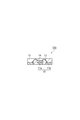
- FIG. 1 is a cross-sectional view showing a temporary protective film according to an embodiment.
- a temporary protective film 10 shown in FIG. 1 includes a support film 1 and an adhesive layer 2 provided on one side of the support film 1. An adhesive layer may be formed on both surfaces of the support film 1.
- FIG. 2 is also a cross-sectional view showing a temporary protective film according to an embodiment.
- the temporary protective film 10 ′ of FIG. 2 is substantially provided on the support film 1, the adhesive layer 2 provided on one main surface of the support film 1, and the other main surface of the support film 1. And a resin layer (non-adhesive layer 3) having no adhesiveness.
- These temporary protective films are used in the sealing molding process for forming a sealing layer for sealing the semiconductor element mounted on the lead frame.
- the lead frame can be used as a temporary protective film for semiconductor sealing molding for temporarily protecting the lead frame during sealing molding.
- the adhesive layer contains acrylic rubber.
- Acrylic rubber is generally a copolymer containing (meth) acrylic acid ester as a monomer unit.
- the acrylic rubber is, for example, a copolymer obtained by a polymerization reaction of a monomer mixture containing (meth) acrylic acid ester and another monomer such as (meth) acrylic acid, an aromatic vinyl compound, and a vinyl cyanide compound. It is a polymer.
- Examples of the (meth) acrylic acid ester constituting the acrylic rubber include butyl (meth) acrylate (for example, n-butyl (meth) acrylate), ethyl (meth) acrylate, and methyl (meth) acrylate. Can be mentioned.
- the (meth) acrylic acid ester may be a compound having a reactive functional group such as 2-hydroxyethyl (meth) acrylate and glycidyl (meth) acrylate.
- the acrylic rubber is mainly composed of at least one (meth) acrylate selected from the group consisting of butyl (meth) acrylate, ethyl (meth) acrylate and methyl (meth) acrylate as a monomer unit.
- the “main component” refers to a monomer unit occupying 50% by mass or more with respect to the total mass of the copolymer.
- acrylic rubber examples include (meth) acrylic acid and acrylonitrile.
- the acrylic rubber contains at least one selected from the group consisting of (meth) acrylic acid and 2-hydroxyethyl (meth) acrylate as a monomer unit
- the acrylic rubber has a carboxy group and / or a hydroxy group. You may have. This carboxy group and / or hydroxy group can be used for the reaction with the below-described peelability-imparting agent.
- the glass transition temperature (Tg) of the acrylic rubber may be ⁇ 50 to 40 ° C., ⁇ 40 ° C. to 30 ° C., or ⁇ 30 ° C. to 20 ° C. from the viewpoint of maintaining the adhesiveness of the adhesive layer at room temperature. .
- the glass transition temperature of the acrylic rubber is ⁇ 50 ° C. or higher, the wettability is reduced by the heat treatment, so that a decrease in peelability tends to be relatively suppressed.
- the glass transition temperature of the acrylic rubber is 20 ° C. or less, there is a tendency that a reduction in sticking property at room temperature is relatively suppressed.
- the glass transition temperature of acrylic rubber is not particularly limited, but generally means a value measured by differential scanning calorimetry, differential calorimetry, dynamic viscoelasticity measurement, or thermomechanical analysis.
- the acrylic rubber is a copolymer having as a main component at least one monomer unit selected from the group consisting of butyl (meth) acrylate, ethyl (meth) acrylate and methyl (meth) acrylate, and
- the glass transition temperature of the acrylic rubber may be ⁇ 30 ° C. to 20 ° C. In this case, the wettability to the adherend is improved, and the adhesiveness and the peelability can be compatible at a particularly high level.
- the weight average molecular weight of the acrylic rubber may be 400,000 or more, 450,000 or more, or 700,000 or more from the viewpoint of low outgassing property and cohesive force maintenance.
- the weight average molecular weight of the acrylic rubber is not particularly limited, but may be 900,000 or less.
- the weight average molecular weight of the acrylic rubber here means a value (converted value by standard polystyrene) measured by gel permeation chromatography.
- acrylic rubber a commercially available product may be used.
- examples of commercially available acrylic rubber include HTR-280 DR (manufactured by Nagase ChemteX Corporation, weight average molecular weight 800,000 to 900,000), WS-023 EK30 (manufactured by Nagase ChemteX Corporation, weight average molecular weight 450,000- 500,000). These acrylic rubbers may be used alone or in combination of two or more.
- the content of the acrylic rubber in the adhesive layer may be 50% by mass or more, 60% by mass or more, 70% by mass or more, or 80% by mass or more, and 100% by mass or less, based on the mass of the adhesive layer. May be.
- the adhesive layer containing acrylic rubber can have a good sticking property at room temperature.
- the adhesive layer can have pressure sensitive adhesion at 24 ° C. without intentionally applying temperature.
- Pressure-sensitive adhesiveness at 24 ° C.” means that the temperature is not intentionally applied.
- an adhesive layer (40 mm ⁇ 160 mm size) and a lead frame (50 mm ⁇ 157 mm size) with a load of 20 N ) Is pressure-bonded to the lead frame of the adhesive layer is 5 N / m or more.
- the said adhesive force can be measured according to the method as described in the below-mentioned Example.
- the solid protective modulus at 200 ° C. of the temporary protective film (hereinafter also simply referred to as “solid shear modulus”) is 5.0 MPa or more.
- the solid shear modulus at 200 ° C. of the temporary protective film may be 6 MPa or more, 8 MPa or more, or 10 MPa or more, or 25 MPa or less, or 20 MPa or less.
- the adhesive residue on the lead frame and the sealing layer after the sealing molding is further suppressed.
- the solid shear modulus is set by placing a test piece of a temporary protective film having a size of 5 mm ⁇ 8 mm on a solid shear measurement jig, and using a dynamic viscoelasticity measuring apparatus (for example, Rhegel-E4000 manufactured by UBM Co., Ltd.). By using, it means a value measured under conditions of a sine wave, 30 to 250 ° C., a heating rate of 5 ° C./min, and a frequency of 400 Hz.
- a laminate comprising a support film and an adhesive layer is used as the test piece.
- the wire bonding step is performed under conditions using ultrasonic waves and pressing pressure while heating at 200 to 270 ° C. for 3 to 60 minutes, for example.
- the adhesive layer becomes soft, there may be a problem that the wires cannot be placed accurately.
- outgas generated by thermal decomposition of the adhesive layer contaminates the semiconductor element and the inner lead surface.
- the solid shear modulus tends to increase as the adhesive layer thickness (film thickness) decreases.
- the thickness of the adhesive layer containing acrylic rubber in the range of 1 to 5 ⁇ m
- the solid shear modulus at 200 ° C. of the temporary protective film can be easily set to 5.0 MPa or more.
- the thickness of the adhesive layer may be 5 ⁇ m or less, or 3 ⁇ m or less from the viewpoint of suppressing or preventing defects during wire bonding (for example, unbonded wires, wire breakage, and insufficient wire bonding strength). From the same viewpoint, the thickness (film thickness) of the adhesive layer may be 1 ⁇ m or more, and may be 2 ⁇ m or more.
- the adhesive layer may further contain a peelability-imparting agent.
- the peelability-imparting agent is a component that lowers the adhesive force of the adhesive layer after sealing molding to the lead frame and / or the sealing layer as compared with the case where the adhesive layer does not contain it.
- An aliphatic compound can be used as the peelability-imparting agent.
- An aliphatic compound is a compound having a linear, branched, or alicyclic hydrocarbon group.
- the aliphatic compound may have at least one functional group selected from the group consisting of an epoxy group and a hydroxy group, and may have an epoxy group.
- the release agent may be an aliphatic epoxy resin.
- the aliphatic compound may be water-soluble.
- the peelability-imparting agent has a hydrocarbon group containing a main chain having 2 or more carbon atoms, which may have a side chain (branching), and an epoxy group bonded to the terminal of the main chain.
- An aliphatic epoxy resin may be included.
- the peelability-imparting agent is at least one aliphatic compound (or aliphatic epoxy resin) selected from the group consisting of (poly) ethylene glycol diglycidyl ether, sorbitol polyglycidyl ether, and glycerol polyglycidyl ether. May be included. These aliphatic compounds may be used alone or in combination of two or more, but may be used in combination of two or more from the viewpoint of further suppressing adhesive residue.
- the acrylic rubber contains at least one selected from the group consisting of (meth) acrylic acid and 2-hydroxyethyl acrylate as a monomer unit, and an aliphatic compound having an epoxy group as a release agent Further, the releasability from the lead frame and the sealing layer becomes even better, and the cleaning process when the adhesive layer remains on the lead frame and the sealing layer becomes more efficient. This is due to the reaction between the epoxy group of the peelability-imparting agent and the hydroxy group and / or carboxy group of the side chain of the acrylic rubber. Presumably, this is due to the increase in cleaning properties triggered by the agent.
- the content of the peelability-imparting agent may be 6 parts by mass or more, or 10 parts by mass or more with respect to 100 parts by mass of the acrylic rubber, and is less than 60 parts by mass, 50 parts by mass or less, or 30 parts by mass or less. There may be.
- the content of the peelability-imparting agent is less than 60 parts by mass, a decrease in adhesion between the adhesive layer and the support film is suppressed, and the adhesive layer tends to be difficult to peel.
- the content of the releasability imparting agent is 6 parts by mass or more, it tends to be easier to ensure sufficient releasability and cleanability.
- the adhesive layer may further contain other components as necessary.
- other components include amino alkyd resins and fatty acids.
- the adhesive strength of the adhesive layer to the lead frame and the sealing layer may be 450 N / m or less after sealing molding, or 300 N / m or less.
- the adhesive force to the lead frame and the sealing layer after the sealing molding can be measured according to the method described in Examples described later.
- the 5% weight reduction temperature of the temporary protective film may be 350 ° C. or higher. As a result, the amount of outgas is reduced and the wire bondability is further improved.
- the 5% weight reduction temperature of the temporary protective film may be 500 ° C. or lower, and may be 450 ° C. or lower.
- the 5% weight loss temperature can be measured using a differential thermal balance (for example, SSC model 5200 manufactured by Seiko Instruments Inc.) under conditions of a heating rate of 10 ° C./min and in an air atmosphere.
- the support film is not particularly limited, but may be a heat resistant resin film.
- a heat resistant resin film is used as the support film, the support film is not softened even under high temperature conditions (for example, 200 ° C. or higher), and the workability is further improved.
- the glass transition temperature (Tg) of the support film may be 200 ° C. or higher, or 250 ° C. or higher from the viewpoint of improving heat resistance.
- the heat-resistant resin constituting the support film includes aromatic polyimide, aromatic polyamide, aromatic polyamideimide, aromatic polysulfone, aromatic polyethersulfone, polyphenylene sulfide, aromatic polyetherketone, polyarylate, aromatic polyether Examples include ether ketone, polyethylene naphthalate, and polyethylene terephthalate.
- the support film may be a polyimide film because it has heat resistance and can further improve the adhesion to the adhesive layer.
- the polyimide film may be subjected to high adhesion treatment such as plasma treatment, corona treatment, and primer treatment.
- high adhesion treatment such as plasma treatment, corona treatment, and primer treatment.
- the thickness (film thickness) of the support film is not particularly limited, but is 100 ⁇ m or less, 50 ⁇ m or less, or from the viewpoint of reducing residual stress related to warping of the lead frame after the temporary protective film is attached to the lead frame, or It may be 25 ⁇ m or less.
- the thickness of the support film may be 5 ⁇ m or more, or 10 ⁇ m or more.
- the support film may have a thickness of 5 ⁇ m to 50 ⁇ m, and the adhesive layer may have a thickness of 1 ⁇ m to 5 ⁇ m.
- the temporary protective film for semiconductor encapsulation molding may include a cover film provided on the surface of the adhesive layer opposite to the surface on which the support film is provided. That is, the temporary protective film for semiconductor encapsulation molding may be in the form of a temporary protective film for semiconductor encapsulation molding with a cover film.
- a polyethylene terephthalate film may be sufficient and the polyethylene terephthalate film which provided the peeling layer may be sufficient.
- the thickness of the cover film may be 10 ⁇ m to 100 ⁇ m, or 20 ⁇ m to 100 ⁇ m.
- the non-adhesive layer 3 included in the temporary protective film 10 ′ according to the embodiment of FIG. 2 is a resin layer that does not substantially have adhesiveness (or pressure-sensitive adhesiveness) to the lead frame at 0 to 270 ° C.
- a resin layer having a high glass transition temperature can function as a non-adhesive layer.
- the non-adhesive layer may be, for example, a resin layer containing polyamideimide.
- the thickness of the non-adhesive layer is not particularly limited, but may be 1 to 10 ⁇ m, for example.
- the temporary protective film which concerns on one Embodiment can be manufactured by the following method, for example. First, acrylic rubber, a solvent such as cyclohexanone and methyl ethyl ketone, and other components such as a peelability-imparting agent as necessary are mixed to prepare a varnish. After apply
- the method for applying the varnish to one side of the support film is not particularly limited, and for example, roll coating, reverse roll coating, gravure coating, bar coating, comma coating, die coating, and vacuum die coating can be used.
- a semiconductor device can be manufactured by the method including the sealing molding process of the semiconductor element using the temporary protective film which concerns on one Embodiment.
- the manufactured semiconductor device has, for example, a lead frame and a semiconductor element mounted on the lead frame, and a sealing layer that seals the semiconductor element on the semiconductor element side of the lead frame, and the back surface of the lead frame is for external connection. It may be a Non Lead Type Package exposed to Specific examples thereof include QFN (QuadFlat Non-Leaded Package) and SON (Small Outline Non-Leaded Package).
- FIG. 3 is a cross-sectional view showing a method for manufacturing a semiconductor device according to an embodiment.
- 4 is a cross-sectional view showing an embodiment of a semiconductor device obtained by the manufacturing method of FIG.
- each process is demonstrated with reference to each drawing as needed.
- the temporary protective film 10 is pasted on one side (back side) of the lead frame 11 having the die pad 11a and the inner lead 11b so that the adhesive layer is in contact with the lead frame.
- a step of peeling the layers is performed by the semiconductor element 14 on the surface of the die pad 11a opposite to the temporary protective film 10.
- the temporary protective film 10 can be attached to the lead frame 11 at room temperature (eg, 5 to 35 ° C.).
- the method of attaching is not particularly limited, but for example, a roll laminating method may be used.
- a lead frame with a temporary protective film includes a lead frame 11 having a die pad 11 a and an inner lead 11 b and a temporary protective film 10, and the temporary protective film 10 has an adhesive layer 2 of the lead frame 11. It is affixed to the lead frame 11 so as to contact one side.
- the material of the lead frame 11 is not particularly limited, but may be, for example, an iron alloy such as 42 alloy, copper, or a copper alloy.
- the surface of the lead frame may be coated with palladium, gold, silver, or the like.
- the surface of the lead frame may be physically roughened. Chemical treatment such as epoxy bleed out (EBO) prevention treatment for preventing bleed out of the silver paste may be performed on the surface of the lead frame.
- EBO epoxy bleed out
- the semiconductor element 14 is usually mounted (adhered) to the die pad 11a via an adhesive (for example, silver paste).
- the adhesive may be cured by heat treatment (for example, 140 to 200 ° C., 30 minutes to 2 hours).
- the wire 12 is not particularly limited, but may be, for example, a gold wire, a copper wire, or a palladium-coated copper wire.
- the semiconductor element and the inner lead may be bonded to the wire 12 using ultrasonic waves and pressing pressure after heating at 200 to 270 ° C. for 3 to 60 minutes.
- the lead frame 11 may be subjected to plasma treatment before the sealing molding step for obtaining the sealing molded body 20 (forming the sealing layer 13).
- the plasma treatment include a method in which a gas such as argon, nitrogen, oxygen, or the like is injected at a predetermined gas flow rate under reduced pressure conditions (eg, 9.33 Pa or less), and plasma irradiation is performed.
- the plasma irradiation output in the plasma treatment may be, for example, 10 to 500 W.
- the plasma treatment time may be, for example, 5 to 50 seconds.
- the gas flow rate in the plasma treatment may be 5 to 50 sccm.
- the sealing layer 13 is formed using a sealing material.
- a sealed molded body 20 having a plurality of semiconductor elements 14 and a sealing layer 13 that collectively seals them is obtained.
- the sealing material is suppressed from going around to the back side of the lead frame 11.
- a sealing molded body with a temporary protective film connects a lead frame 11 having a die pad 11a and an inner lead 11b, a semiconductor element 14 mounted on the die pad 11a, and the semiconductor element 14 and the inner lead 11b.
- a wire 12, a semiconductor element 14, a sealing layer 13 that seals the wire 12, and a temporary protective film 10 are provided, and the temporary protective film 10 has an adhesive layer 2 of the semiconductor element 14 of the lead frame 11. It is affixed to the surface opposite to the mounted surface.
- the temperature (sealing temperature) during the formation of the sealing layer may be 140 to 200 ° C. or 160 to 180 ° C.
- the pressure during the formation of the sealing layer (sealing pressure) may be 6-15 MPa or 7-10 MPa.
- the heating time (sealing time) in the sealing molding may be 1 to 5 minutes or 2 to 3 minutes.
- the formed sealing layer 13 may be heat-cured as necessary.
- the heating temperature (sealing curing temperature) for curing the sealing layer may be 150 to 200 ° C. or 160 to 180 ° C.
- the heating time (sealing curing time) for curing the sealing layer may be 4 to 7 hours or 5 to 6 hours.
- the material of the sealing material is not particularly limited, and examples thereof include epoxy resins such as cresol novolac epoxy resin, phenol novolac epoxy resin, biphenyl diepoxy resin, and naphthol novolac epoxy resin.
- epoxy resins such as cresol novolac epoxy resin, phenol novolac epoxy resin, biphenyl diepoxy resin, and naphthol novolac epoxy resin.
- a filler, a flame retardant substance such as a bromo compound, and an additive such as a wax component may be added.
- the temporary protective film 10 is peeled from the lead frame 11 and the sealing layer 13 of the obtained sealing molded body 20.
- the temporary protective film 10 may be peeled off at any time before or after the sealing layer is cured.
- the temperature at which the temporary protective film is peeled is not particularly limited, but may be room temperature (eg, 5 to 35 ° C.). This temperature may be equal to or higher than the glass transition temperature of the adhesive layer. In this case, the peelability of the temporary protective film from the lead frame and the sealing material becomes even better.
- the Tg of the acrylic rubber in the adhesive layer is, for example, 5 ° C. or lower, or 0 ° C. or lower, the Tg of the adhesive layer becomes equal to or lower than normal temperature, and good peelability at normal temperature is easily obtained.
- the manufacturing method of the semiconductor device may further include a step of removing the adhesive layer (glue residue) remaining on the lead frame 11 and the sealing layer 13 after the peeling step, if necessary.
- the remaining adhesive layer can be removed using a solvent.
- the solvent for example, dimethyl sulfoxide, ethylene glycol, and water can be used.
- a solvent may be used individually by 1 type and may be used in mixture of 2 or more types.
- a surfactant may be added to the solvent.
- the solvent may be a solution adjusted to be alkaline (alkaline solution). The pH of the alkaline solution may be 10 or higher, or 12 or higher.
- mechanical brushing may be performed as necessary. Further, the burr and oxide film of the sealing layer may be removed.
- the sealing molded body 20 can be divided as necessary to obtain a plurality of semiconductor devices 100 of FIG. 4 each having one semiconductor element. it can.
- the manufacturing method according to the embodiment includes the temporary protective film 10 from the sealed molded body 20.
- the process may further include a step of obtaining the semiconductor device 100 having one die pad 11a and the semiconductor element 14 by dividing the sealing molded body 20 before or after peeling.
- a semiconductor device manufactured using a temporary protective film according to an embodiment is excellent in terms of high density, small area, thinning, and the like, for example, electronic devices such as a mobile phone, a smartphone, a personal computer, and a tablet. Can be suitably used.
- Acrylic rubber / acrylic rubber Ai (manufactured by Nagase ChemteX Corporation, trade name: WS-023 EK30, weight average molecular weight: 500,000)
- Acrylic rubber Aii (manufactured by Nagase ChemteX Corporation, trade name: HTR-280 DR, weight average molecular weight: 900,000)
- Peelability imparting agent Bi (manufactured by Nagase ChemteX Corporation, trade name: EX-614B, sorbitol polyglycidyl ether, epoxy equivalent: 174) Peelability imparting agent Bii (manufactured by Nagase ChemteX Corporation, trade name: EX-810, ethylene glycol diglycidyl ether, epoxy equivalent: 113)
- the test piece obtained by cutting the temporary protective film into a size of 5 mm ⁇ 8 mm is set on a solid shear measuring jig, and a dynamic viscoelasticity measuring device (Rheogel-E4000, manufactured by UBM Co., Ltd.) is used.
- the solid shear modulus was measured under the conditions of a sine wave, 30 to 250 ° C., a heating rate of 5 ° C./min, and a frequency of 400 Hz.
- the input thickness was fixed at 0.1 mm, and the strain control was 1.95 ⁇ m and 1.95%. From the measurement results, the solid shear modulus at 200 ° C. was read.
- Example 14 A temporary protective film of Example 14 was obtained in the same manner as Example 1 except that the thickness of the adhesive layer was 1 ⁇ m.
- the temporary protective film had a solid shear modulus at 200 ° C. of 8.2 MPa.
- Example 15 A temporary protective film of Example 15 was obtained in the same manner as Example 1 except that the thickness of the adhesive layer was 5 ⁇ m.
- the temporary protective film had a solid shear modulus at 200 ° C. of 5.7 MPa.
- Comparative Example 1 A temporary protective film of Comparative Example 1 was obtained in the same manner as in Example 1 except that the thickness of the adhesive layer was 6 ⁇ m.
- the temporary protective film had a solid shear modulus at 200 ° C. of 4.0 MPa.
- Comparative Example 2 A temporary protective film of Comparative Example 2 was obtained in the same manner as in Example 1 except that the thickness of the adhesive layer was 8 ⁇ m.
- the temporary protective film had a solid shear modulus at 200 ° C. of 3.1 MPa.
- Comparative Example 3 A temporary protective film of Comparative Example 3 was obtained in the same manner as in Example 1 except that the thickness of the adhesive layer was 10 ⁇ m.
- the temporary protective film had a solid shear modulus at 200 ° C. of 1.8 MPa.
- Comparative Example 4 Varnish O was applied onto a support film (manufactured by Toray DuPont Co., Ltd., trade name: Kapton 100EN, film thickness: 25 ⁇ m). The coating film was dried by heating at 90 ° C. for 2 minutes and 150 ° C. for 2 minutes to form an adhesive layer having a thickness of 5 ⁇ m on the support film, whereby a temporary protective film of Comparative Example 4 was obtained.
- the temporary protective film had a solid shear modulus at 200 ° C. of 3.2 MPa.
- this solution was cooled to 0 ° C., and 149.5 g (0.71 mol) of trimellitic anhydride chloride was added at this temperature. After the trimellitic anhydride chloride was dissolved, 100 g of triethylamine was added. After stirring at room temperature for 2 hours, the temperature was raised to 180 ° C. and the imidization was completed by a reaction for 5 hours. The reaction solution was poured into methanol to isolate the polymer. This was dried, dissolved in N-methyl-2-pyrrolidone, and poured into methanol to again isolate the polymer. The isolated polymer was dried under reduced pressure to obtain a purified polyetheramideimide powder.
- Varnish P was coated on a support film (polyimide film, Ube Industries, Ltd., trade name: UPILEX25SGA, film thickness: 25 ⁇ m), dried by heating at 100 ° C., 10 minutes, 300 ° C., and 10 minutes to obtain a film thickness. Formed an adhesive layer of 8 ⁇ m.
- the varnish Q was apply
- the temporary protective film had a solid shear modulus of 21.0 MPa.
- each temporary protective film was peeled off at a speed of 50 mm / min in the direction of 180 ° with a force gauge, and the maximum value of the load at that time was recorded as the adhesive force.
- the pressure applied to the tape was 6 MPa, and the pressure was applied for 10 seconds.
- the adhesive layer was affixed to the lead frame by the same method (the same applies to the following adhesive force measurement).
- each temporary protective film was peeled off at a speed of 50 mm / min in the direction of 180 ° with a force gauge, and the maximum value of the load at that time was recorded as the adhesive force. Thereby, the peelability of each temporary protective film from the lead frame after the heat treatment under conditions corresponding to sealing molding was evaluated.
- a CDA194 frame (Cu, manufactured by Shinko Electric Industries Co., Ltd.) was prepared.
- the temporary protective films of the examples and comparative examples are in the direction in which the adhesive layer (40 mm x 160 mm size) is in contact with the lead frame, at room temperature (24 ° C) And pasted under the condition of a load of 20N.
- the lead frame and the temporary protective film were heated in an oven in an air atmosphere while changing the conditions in the order of 180 ° C. for 60 minutes and 200 ° C. for 60 minutes.
- a sealing layer was formed by a trade name: GE-7470LA, manufactured by Hitachi Chemical Co., Ltd.
- each temporary protective film is peeled off at a speed of 50 mm / min in the direction of 180 ° with a force gauge, and the maximum load when the adhesive layer is peeled off from the sealing layer is determined with respect to the sealing layer after sealing molding. Recorded as adhesion. Thereby, the peelability from the sealing layer after sealing molding of each temporary protective film was evaluated.
- the lead frame and the temporary protective film were heated in an oven in an air atmosphere while changing the conditions in the order of 180 ° C. for 60 minutes and 200 ° C. for 60 minutes.
- Plasma treatment was performed on the surface of the lead frame opposite to the temporary protective film in an argon gas atmosphere (flow rate: 20 sccm) under conditions of 150 W and 15 seconds.
- a molding machine manufactured by Apic Yamada Co., Ltd.
- sealing molding is performed under the conditions of 175 ° C., 6.8 MPa, and 2 minutes, and the sealing material is formed on the surface of the lead frame opposite to the temporary protective film.
- a sealing layer was formed by (trade name: GE-7470LA, manufactured by Hitachi Chemical Co., Ltd.).
- each temporary protective film was peeled off at a speed of 50 mm / min in the 180 ° direction with a force gauge, and the maximum load when the adhesive layer is peeled off from the lead frame or the sealing layer is Was recorded as the adhesive strength to the lead frame or the sealing layer. Thereby, the peelability after sealing layer hardening of each temporary protective film was evaluated.
- Adhesive residue The temporary protective films of Examples and Comparative Examples are placed on a CDA194 frame (lead frame, manufactured by Shinko Electric Industries Co., Ltd.) at a normal temperature (24 ° C.) and a load of 20 N with the adhesive layer in contact with the lead frame. Pasted with conditions.
- the lead frame and the temporary protective film were heated in an oven in an air atmosphere while changing the conditions in the order of 180 ° C. for 60 minutes and 200 ° C. for 60 minutes.
- Plasma treatment was performed on the surface of the lead frame opposite to the temporary protective film under an argon gas atmosphere (flow rate: 20 sccm) at 150 W for 15 seconds.
- sealing molding is performed under the conditions of 175 ° C., 6.8 MPa, 2 minutes, and the sealing material (product) on the surface of the lead frame opposite to the temporary protective film Name: GE-7470LA, manufactured by Hitachi Chemical Co., Ltd.) to form a sealing layer. Thereafter, each temporary protective film was peeled off at a speed of 50 mm / min in the direction of 180 °, and the state of the adhesive layer on the sealing layer and the lead frame after peeling was confirmed. Based on the area ratio of the portion where the adhesive residue was present with respect to the total area of the sealing layer and the lead frame surface, the adhesive residue was evaluated in six stages according to the following criteria. 5: 60 to 100% (the remaining adhesive layer is generally relatively thick) 4: 60-100% (remaining adhesive layer is generally relatively thin) 3: 30% or more and less than 60% 2: 10% or more and less than 30% 1: Over 1% and less than 10% 0: 0%
- the above evaluation results are shown in Tables 3 and 4.
- the temporary protective film of each example can be attached to the lead frame at room temperature, and can be easily peeled off from the lead frame and the sealing layer while suppressing adhesive residue after the sealing molding.
- SYMBOLS 1 Support film, 2 ... Adhesive layer, 3 ... Non-adhesion layer, 10, 10 '... Temporary protective film, 11 ... Lead frame, 11a ... Die pad, 11b ... Inner lead, 12 ... Wire, 13 ... Sealing layer, 14 ... Semiconductor element, 20 ... Sealed molded body, 100 ... Semiconductor device.
Landscapes
- Chemical & Material Sciences (AREA)
- Organic Chemistry (AREA)
- Encapsulation Of And Coatings For Semiconductor Or Solid State Devices (AREA)
- Adhesives Or Adhesive Processes (AREA)
- Lead Frames For Integrated Circuits (AREA)
- Adhesive Tapes (AREA)
- Laminated Bodies (AREA)
- Manufacture Of Macromolecular Shaped Articles (AREA)
- Structures Or Materials For Encapsulating Or Coating Semiconductor Devices Or Solid State Devices (AREA)
Abstract
Description
また、特許文献1の半導体用接着フィルムは、封止後の剥離のために加熱処理を行うことが好ましい。一方、常温での貼り付け性が比較的良好なフィルムの場合、封止後のリードフレーム及び封止材からの剥離の際、リードフレーム側に糊残りが発生する場合がある等、封止成形後の剥離性の点で改善の余地があった。
図1は、一実施形態に係る仮保護フィルムを示す断面図である。図1に示す仮保護フィルム10は、支持フィルム1と、支持フィルム1の片面上に設けられた接着層2と、から構成される。支持フィルム1の両面上に接着層が形成されていてもよい。図2も、一実施形態に係る仮保護フィルムを示す断面図である。図2の仮保護フィルム10’は、支持フィルム1と、支持フィルム1の一方の主面上に設けられた接着層2と、支持フィルム1の他方の主面上に設けられた、実質的に接着性を有しない樹脂層(非接着層3)とを有する。これらの仮保護フィルムは、リードフレームに搭載された半導体素子を封止する封止層を形成する封止成形の工程において、リードフレームの裏面(半導体素子が搭載される面とは反対側の面)に貼り付けることで、リードフレームを封止成形の間、仮保護するための半導体封止成形用仮保護フィルムとして用いることができる。
接着層は、アクリルゴムを含有する。アクリルゴムは、一般に、(メタ)アクリル酸エステルを単量体単位として含む共重合体である。アクリルゴムは、例えば、(メタ)アクリル酸エステルと、(メタ)アクリル酸、芳香族ビニル化合物、シアン化ビニル化合物等の他の単量体とを含む単量体混合物の重合反応により得られる共重合体である。
支持フィルムは、特に制限されないが、耐熱性樹脂フィルムであってもよい。支持フィルムとして耐熱性樹脂フィルムを用いる場合、高温条件(例えば、200℃以上)であっても、支持フィルムが軟化せず、作業性がより一層優れたものとなる。具体的には、支持フィルムのガラス転移温度(Tg)が、耐熱性向上の観点から、200℃以上、又は250℃以上であってもよい。
上記半導体封止成形用仮保護フィルムは、上記接着層の上記支持フィルムが設けられた面とは反対側の面上に設けられたカバーフィルムを備えていてよい。つまり、上記半導体封止成形用仮保護フィルムは、カバーフィルム付き半導体封止成形用仮保護フィルムの形態であってもよい。上記カバーフィルムは、特に制限はないが、ポリエチレンテレタレートフィルムであってもよく、剥離層を設けたポリエチレンテレフタレートフィルムであってもよい。
一実施形態に係る仮保護フィルムは、例えば、以下の方法により製造することができる。まず、アクリルゴムと、シクロヘキサノン、メチルエチルケトン等の溶剤と、必要に応じて剥離性付与剤等の他の成分と、を混合し、ワニスを作製する。作製したワニスを支持フィルムの片面に塗布した後、加熱処理により塗膜から溶剤を除去して、支持フィルム上に接着層を形成する。これにより、二層構造の仮保護フィルムを得ることができる。
一実施形態に係る仮保護フィルムを用いた半導体素子の封止成形工程を含む方法によって、半導体装置を製造することができる。製造される半導体装置は、例えば、リードフレーム及びこれに搭載された半導体素子と、リードフレームの半導体素子側で半導体素子を封止する封止層とを有し、リードフレームの裏面が外部接続用に露出している、Non Lead Type Packageであってもよい。その具体例としては、QFN(QuadFlat Non-leaded Package)、SON(Small Outline Non-leaded Package)が挙げられる。
(塗工用ワニスの作製)
表1又は表2に示す組成(単位:質量部)を有する樹脂組成物に、溶剤としてシクロヘキサノンを加えて攪拌混合し、不揮発分12質量%のワニスA~Oを得た。表に示すアクリルゴム及び剥離性付与剤の詳細は以下のとおりである。
アクリルゴム
・アクリルゴムAi(ナガセケムテックス株式会社製、商品名:WS-023 EK30、重量平均分子量:50万)
・アクリルゴムAii(ナガセケムテックス株式会社製、商品名:HTR-280 DR、重量平均分子量:90万)
・剥離性付与剤Bi(ナガセケムテックス株式会社製、商品名:EX-614B、ソルビトールポリグリシジルエーテル、エポキシ当量:174)
・剥離性付与剤Bii(ナガセケムテックス株式会社製、商品名:EX-810、エチレングリコールジグリシジルエーテル、エポキシ当量:113)


実施例1~13
得られたワニスA~Mをそれぞれ支持フィルム(ポリイミドフィルム、宇部興産株式会社製、商品名:UPILEX25SGA、膜厚:25μm)上に塗布した。塗膜を90℃で2分間、及び150℃で2分間加熱することによって乾燥し、支持フィルム上に厚さ2μmの接着層を形成し、実施例1~13の仮保護フィルムを得た。実施例1~13の各仮保護フィルムにおいて、200℃における固体せん断弾性率を下記の方法で測定した。結果を表3に示した。
仮保護フィルムを5mm×8mmサイズに切って得た試験片を固体せん断測定ジグにセットし、動的粘弾性測定装置(株式会社ユービーエム製、Rheogel-E4000)を用いて、正弦波、30~250℃、昇温速度5℃/min、周波数400Hzの条件で固体せん断弾性率を測定した。なお、入力厚みは0.1mmで固定し、歪み制御1.95μm、1.95%とした。測定結果から、200℃における固体せん断弾性率を読み取った。
接着層の厚さを1μmとすること以外は実施例1と同様にして、実施例14の仮保護フィルムを得た。仮保護フィルムの200℃における固体せん断弾性率は8.2MPaであった。
接着層の厚さを5μmとすること以外は実施例1と同様にして、実施例15の仮保護フィルムを得た。仮保護フィルムの200℃における固体せん断弾性率は5.7MPaであった。
接着層の厚さを6μmとすること以外は実施例1と同様にして、比較例1の仮保護フィルムを得た。仮保護フィルムの200℃における固体せん断弾性率は4.0MPaであった。
接着層の厚さを8μmとすること以外は実施例1と同様にして、比較例2の仮保護フィルムを得た。仮保護フィルムの200℃における固体せん断弾性率は3.1MPaであった。
接着層の厚さを10μmとすること以外は実施例1と同様にして、比較例3の仮保護フィルムを得た。仮保護フィルムの200℃における固体せん断弾性率は1.8MPaであった。
ワニスOを支持フィルム(東レ・デュポン株式会社製、商品名:カプトン100EN、膜厚:25μm)上に塗布した。塗膜を90℃で2分間、及び150℃で2分間加熱することによって乾燥し、支持フィルム上に厚さ5μmの接着層を形成し、比較例4の仮保護フィルムを得た。仮保護フィルムの200℃における固体せん断弾性率は3.2MPaであった。
(塗工用ワニスの作製)
温度計、撹拌機、窒素導入管及び分留塔をとりつけた5リットルの4つ口フラスコに窒素雰囲気下、2,2-ビス[4-(4-アミノフェノキシ)フェニル]プロパン270.9g(0.66モル)、1,3-ビス(3-アミノプロピル)-テトラメチルジシロキサン8.7g(0.035 モル)を入れ、これらをN-メチル-2-ピロリドン1950gに溶解した。さらにこの溶液を0℃に冷却し、この温度で無水トリメリット酸クロライド149.5g(0.71モル)を添加した。無水トリメリット酸クロライドが溶解した後、トリエチルアミン100gを添加した。室温で2時間撹拌を続けた後、180℃に昇温して5時間の反応によりイミド化を完結させた。反応液をメタノール中に投入して重合体を単離した。これを乾燥した後、N-メチル-2-ピロリドンに溶解しメタノール中に投入して再度重合体を単離した。単離した重合体を減圧乾燥して精製された粉末状のポリエーテルアミドイミドを得た。このポリエーテルアミドイミド120gとシランカップリング剤(東レ・ダウコーニング株式会社製、商品名:SH6040)3.6gをN-メチル-2-ピロリドン360gに溶解し、接着層形成用のワニスPを得た。
ワニスPを支持フィルム(ポリイミドフィルム、宇部興産株式会社製、商品名:UPILEX25SGA、膜厚:25μm)上に塗布し、100℃、10分間及び300℃、10分間の加熱により乾燥して、膜厚が8μmの接着層を形成した。次に接着剤ワニスを塗布した支持フィルムの裏面にワニスQを塗布し、100℃、10分間及び300℃、10分間の加熱により乾燥して、膜厚が6μmの非接着層を形成した。これにより、接着層及び非接着層を有する比較例5の仮保護フィルムを得た。仮保護フィルムの固体せん断弾性率は21.0MPaであった。
(接着層の接着力)
(1)常温貼り付け後(常温での貼り付け性)
リードフレームとして、CDA194フレーム(Cu、新光電気工業株式会社製)、及びCDA194パラジウムメッキフレーム(PPF、新光電気工業株式会社製)を準備した。これらリードフレーム(50mm×157mmサイズ)に、ハンドローラーを用いて、実施例及び比較例の各仮保護フィルムを、接着層(40mm×160mmサイズ)がリードフレームに接する向きで、常温(24℃)、荷重20Nの条件で貼り付けた。その後、フォースゲージにて180°方向に50mm/分の速度で各仮保護フィルムを引き剥がし、そのときの荷重の最大値を接着力として記録した。これにより、各仮保護フィルムの常温での貼り付け性(感圧接着性)を評価した。
ただし、比較例5の仮保護フィルムの場合、接着層の常温での貼り付け性が弱かったため、230℃に加熱されたプレス機を用いて、テープにかかる圧力を6MPaとし、10秒間加圧することで接着層をリードフレームに貼り付けた(以下の接着力測定でも同様)。
リードフレームとして、CDA194フレーム(Cu、新光電気工業株式会社製)、及びCDA194パラジウムメッキフレーム(PPF、新光電気工業株式会社製)を準備した。これらリードフレーム(50mm×157mmサイズ)に、ハンドローラーを用いて、実施例及び比較例の各仮保護フィルムを、接着層(40mm×160mmサイズ)がリードフレームに接する向きで、常温(24℃)、荷重20Nの条件で貼り付けた。その後、リードフレーム及び仮保護フィルムを、空気雰囲気下、オーブン内で、180℃で60分間、200℃で60分間、175℃で2分間の順で条件を変更しながら加熱した。その後、フォースゲージにて180°方向に50mm/分の速度で各仮保護フィルムを引き剥がし、そのときの荷重の最大値を接着力として記録した。これにより、各仮保護フィルムの、封止成形に相当する条件における加熱処理後のリードフレームからの剥離性を評価した。
リードフレームとして、CDA194フレーム(Cu、新光電気工業株式会社製)を準備した。上記リードフレーム(50mm×157mmサイズ)に、ハンドローラーを用いて、実施例及び比較例の各仮保護フィルムを、接着層(40mm×160mmサイズ)がリードフレームに接する向きで、常温(24℃)、荷重20Nの条件で貼り付けた。その後、リードフレーム及び仮保護フィルムを、空気雰囲気下、オーブン内で、180℃で60分間、200℃で60分間の順で条件を変えながら加熱した。
次いで、リードフレームの仮保護フィルムとは反対側の面上にプラズマ処理をアルゴンガス雰囲気下(流量:20sccm)、150W、15秒の条件で行った。その後、モールド成形機(アピックヤマダ株式会社製)を用いて175℃、6.8MPa、2分間の条件で封止成形を行い、リードフレームの仮保護フィルムとは反対側の面上に封止材(商品名:GE-7470L-A、日立化成株式会社製)により封止層を形成した。
その後フォースゲージにて180°方向に50mm/分の速度で各仮保護フィルムを引き剥がし、接着層が封止層から引き剥がされるときの荷重の最大値を、封止成形後の封止層に対する接着力として記録した。これにより、各仮保護フィルムの封止成形後の封止層からの剥離性を評価した。
リードフレームとして、CDA194フレーム(Cu、新光電気工業株式会社製)、及びCDA194パラジウムメッキフレーム(PPF、新光電気工業株式会社製)を準備した。これらリードフレーム(50mm×157mmサイズ)に、ハンドローラーを用いて、実施例及び比較例の各仮保護フィルムを、接着層(40mm×160mmサイズ)がリードフレームに接する向きで、常温(24℃)、荷重20Nの条件で貼り付けた。その後、リードフレーム及び仮保護フィルムを空気雰囲気下、オーブン内で、180℃で60分間、200℃で60分間の順で条件を変えながら加熱した。リードフレームの仮保護フィルムとは反対側の面上に、プラズマ処理をアルゴンガス雰囲気下(流量:20sccm)、150W、15秒の条件で行った。次いで、モールド成形機(アピックヤマダ株式会社製)を用いて、175℃、6.8MPa、2分間の条件で封止成形を行い、リードフレームの仮保護フィルムとは反対側の面上に封止材(商品名:GE-7470L-A、日立化成株式会社製)により封止層を形成した。さらに、オーブン中、空気雰囲気下で180℃、5時間の加熱により、封止層を硬化させた。加熱後、フォースゲージにて180°方向に50mm/分の速度で各仮保護フィルムを引き剥がし、接着層がリードフレーム又は封止層から引き剥がされるときの荷重の最大値を、封止成形後のリードフレーム又は封止層に対する接着力としてそれぞれ記録した。これにより、各仮保護フィルムの封止層硬化後の剥離性を評価した。
CDA194フレーム(リードフレーム、新光電気工業株式会社製)に、実施例及び比較例の仮保護フィルムを、接着層がリードフレームに接する向きで、常温(24℃)、荷重20Nの条件で貼りつけた。リードフレーム及び仮保護フィルムを、空気雰囲気下、オーブン内で、180℃で60分間、200℃で60分の順で条件を変更しながら加熱した。リードフレームの仮保護フィルムとは反対側の面上にプラズマ処理をアルゴンガス雰囲気下(流量:20sccm)、150W、15秒の条件で行った。
モールド成形機(アピックヤマダ株式会社製)を用いて、175℃、6.8MPa、2分間の条件で封止成形を行い、リードフレームの仮保護フィルムとは反対側の面上に封止材(商品名:GE-7470L-A、日立化成株式会社製)により封止層を形成した。
その後180°方向に50mm/分の速度で各仮保護フィルムを引き剥がし、引き剥がした後の封止層及びリードフレーム上の糊残りの状態を確認した。封止層及びリードフレームの表面を合わせた全体の面積に対する、糊残りがあった部分の面積割合に基づいて、以下の基準で6段階で糊残りを評価した。
5:60~100%(残っている接着層が全般に比較的厚い)
4:60~100%(残っている接着層が全般に比較的薄い)
3:30%以上60%未満
2:10%以上30%未満
1:0%超10%未満
0:0%
実施例及び比較例の各仮保護フィルムの5%重量減少温度を、示差熱天秤(セイコーインスツル株式会社製、SSC5200型)を用いて、空気雰囲気下、昇温速度10℃/分の条件で測定した。


Claims (14)
- 支持フィルムと、前記支持フィルム上に設けられ、アクリルゴムを含有する接着層と、を備える、半導体封止成形用仮保護フィルムであって、
前記仮保護フィルムの200℃における固体せん断弾性率が、5.0MPa以上である、半導体封止成形用仮保護フィルム。 - 前記接着層が、剥離性付与剤を更に含有する、請求項1に記載の半導体封止成形用仮保護フィルム。
- 前記剥離性付与剤の含有量が、前記アクリルゴム100質量部に対して6質量部以上60質量部未満である、請求項2に記載の半導体封止成形用仮保護フィルム。
- 前記接着層の厚さが、1μm以上5μm以下である、請求項1~3のいずれか一項に記載の半導体封止成形用仮保護フィルム。
- 前記支持フィルムが、ポリイミドフィルムである、請求項1~4のいずれか一項に記載の半導体封止成形用仮保護フィルム。
- 前記アクリルゴムが、(メタ)アクリル酸ブチル、(メタ)アクリル酸エチル、(メタ)アクリル酸メチル、(メタ)アクリル酸、アクリロニトリル、(メタ)アクリル酸2-ヒドロキシエチル及び(メタ)アクリル酸グリシジルからなる群より選択される少なくとも1種の単量体単位を含む共重合体である、請求項1~5のいずれか一項に記載の半導体封止成形用仮保護フィルム。
- 前記アクリルゴムの重量平均分子量が、450000以上900000以下である、請求項1~6のいずれか一項に記載の半導体封止成形用仮保護フィルム。
- 前記接着層が、24℃において感圧接着性を有する、請求項1~7のいずれか一項に記載の半導体封止成形用仮保護フィルム。
- 前記仮保護フィルムの5%重量減少温度が、350℃以上である、請求項1~8のいずれか一項に記載の半導体封止成形用仮保護フィルム。
- 前記接着層の前記支持フィルムが設けられた面とは反対側の面上に設けられたカバーフィルムを更に備える、請求項1~9のいずれか一項に記載の半導体封止成形用仮保護フィルム。
- ダイパッド及びインナーリードを有するリードフレームと、
請求項1~10のいずれか一項に記載の半導体封止成形用仮保護フィルムと、
を備え、
前記仮保護フィルムが、その接着層が前記リードフレームの片面に接するように前記リードフレームに貼り付けられている、仮保護フィルム付きリードフレーム。 - ダイパッド及びインナーリードを有するリードフレームと、
前記ダイパッドに搭載された半導体素子と、
前記半導体素子と前記インナーリードとを接続するワイヤと、
前記半導体素子及び前記ワイヤを封止している封止層と、
請求項1~10のいずれか一項に記載の半導体封止成形用仮保護フィルムと、
を備え、
前記仮保護フィルムが、その接着層が前記リードフレームの前記半導体素子が搭載されている面とは反対側の面に貼り付けられている、仮保護フィルム付き封止成形体。 - ダイパッド及びインナーリードを有するリードフレームの片面に、請求項1~10のいずれか一項に記載の半導体封止成形用仮保護フィルムを、その接着層が前記リードフレームに接する向きで貼り付ける工程と、
前記ダイパッドの前記仮保護フィルムとは反対側の面上に半導体素子を搭載する工程と、
前記半導体素子と前記インナーリードとを接続するワイヤを設ける工程と、
前記半導体素子及び前記ワイヤを封止する封止層を形成して、前記リードフレーム、前記半導体素子及び前記封止層を有する封止成形体を得る工程と、
前記封止成形体から前記仮保護フィルムを剥離する工程と、
をこの順に備える、半導体装置を製造する方法。 - 前記リードフレームが複数の前記ダイパッドを有し、前記複数のダイパッドの各々に前記半導体素子が搭載され、
当該方法が、前記仮保護フィルムを前記封止成形体から剥離する前又は後に前記封止成形体を分割して、1個の前記ダイパッド及び前記半導体素子を有する半導体装置を得る工程を更に備える、請求項13に記載の方法。
Priority Applications (7)
| Application Number | Priority Date | Filing Date | Title |
|---|---|---|---|
| KR1020197031729A KR102455209B1 (ko) | 2017-05-10 | 2018-01-25 | 반도체 밀봉 성형용 가보호 필름 |
| SG11201910104U SG11201910104UA (en) | 2017-05-10 | 2018-01-25 | Temporary protective film for semiconductor sealing molding |
| JP2019516890A JP7143845B2 (ja) | 2017-05-10 | 2018-01-25 | 半導体封止成形用仮保護フィルム |
| MYPI2019006174A MY193912A (en) | 2017-05-10 | 2018-01-25 | Temporary protective film for semiconductor sealing molding |
| CN201880030197.XA CN110603624B (zh) | 2017-05-10 | 2018-01-25 | 半导体密封成形用临时保护膜 |
| US16/612,106 US11195728B2 (en) | 2017-05-10 | 2018-01-25 | Temporary protective film for semiconductor sealing molding |
| PH12019502491A PH12019502491A1 (en) | 2017-05-10 | 2019-11-05 | Temporary protective film for semiconductor sealing molding |
Applications Claiming Priority (2)
| Application Number | Priority Date | Filing Date | Title |
|---|---|---|---|
| JP2017-094157 | 2017-05-10 | ||
| JP2017094157 | 2017-05-10 |
Publications (1)
| Publication Number | Publication Date |
|---|---|
| WO2018207408A1 true WO2018207408A1 (ja) | 2018-11-15 |
Family
ID=64105158
Family Applications (1)
| Application Number | Title | Priority Date | Filing Date |
|---|---|---|---|
| PCT/JP2018/002313 Ceased WO2018207408A1 (ja) | 2017-05-10 | 2018-01-25 | 半導体封止成形用仮保護フィルム |
Country Status (9)
| Country | Link |
|---|---|
| US (1) | US11195728B2 (ja) |
| JP (1) | JP7143845B2 (ja) |
| KR (1) | KR102455209B1 (ja) |
| CN (1) | CN110603624B (ja) |
| MY (1) | MY193912A (ja) |
| PH (1) | PH12019502491A1 (ja) |
| SG (1) | SG11201910104UA (ja) |
| TW (1) | TWI793101B (ja) |
| WO (1) | WO2018207408A1 (ja) |
Cited By (7)
| Publication number | Priority date | Publication date | Assignee | Title |
|---|---|---|---|---|
| JP6744004B1 (ja) * | 2019-09-17 | 2020-08-19 | 日立化成株式会社 | 仮保護フィルム、リール体、包装体、梱包体、仮保護体、及び、半導体装置を製造する方法 |
| WO2020255975A1 (ja) * | 2019-06-19 | 2020-12-24 | 昭和電工マテリアルズ株式会社 | 半導体封止成形用仮保護フィルム、仮保護フィルム付きリードフレーム、仮保護フィルム付き封止成形体、及び半導体装置を製造する方法 |
| JPWO2021206058A1 (ja) * | 2020-04-06 | 2021-10-14 | ||
| WO2021206069A1 (ja) * | 2020-04-06 | 2021-10-14 | 昭和電工マテリアルズ株式会社 | 半導体封止成形用仮保護フィルム及びその製造方法、仮保護フィルム付きリードフレーム、仮保護された封止成形体、並びに、半導体パッケージを製造する方法 |
| JP2021166227A (ja) * | 2020-04-06 | 2021-10-14 | 昭和電工マテリアルズ株式会社 | 半導体封止成形用仮保護フィルム及びその製造方法、仮保護フィルム付きリードフレーム、封止成形体、並びに、半導体パッケージを製造する方法 |
| JP2022104608A (ja) * | 2020-12-28 | 2022-07-08 | イノックス・アドバンスト・マテリアルズ・カンパニー・リミテッド | Qfn半導体パッケージ用マスクシート |
| US12398298B2 (en) | 2018-11-09 | 2025-08-26 | Resonac Corporation | Temporary protective film for producing semiconductor device, reel body, and method for producing semiconductor device |
Families Citing this family (2)
| Publication number | Priority date | Publication date | Assignee | Title |
|---|---|---|---|---|
| WO2019176599A1 (ja) * | 2018-03-12 | 2019-09-19 | 日立化成株式会社 | リール体、包装体及び梱包物 |
| JP7521184B2 (ja) * | 2019-10-31 | 2024-07-24 | 株式会社レゾナック | 基板搬送用サポートテープ及び電子機器装置の製造方法 |
Citations (4)
| Publication number | Priority date | Publication date | Assignee | Title |
|---|---|---|---|---|
| JP2003086614A (ja) * | 2001-09-12 | 2003-03-20 | Hitachi Chem Co Ltd | 半導体装置の製造方法、半導体用接着・剥離フィルム、これを用いたリードフレーム及び半導体装置 |
| JP2005116919A (ja) * | 2003-10-10 | 2005-04-28 | Nitto Denko Corp | 半導体装置の製造方法及び半導体装置製造用粘着テープ又はシート |
| JP2008131006A (ja) * | 2006-11-24 | 2008-06-05 | Nitto Denko Corp | 半導体装置製造用の耐熱性粘着テープ |
| JP2009044010A (ja) * | 2007-08-09 | 2009-02-26 | Nitto Denko Corp | 半導体装置の製造方法 |
Family Cites Families (5)
| Publication number | Priority date | Publication date | Assignee | Title |
|---|---|---|---|---|
| DE60025720T2 (de) * | 1999-06-18 | 2006-11-09 | Hitachi Chemical Co., Ltd. | Klebstoff, klebstoffgegenstand, schaltungssubstrat für halbleitermontage mit einem klebstoff und eine halbleiteranordnung die diesen enthält |
| JP3501692B2 (ja) | 1999-07-15 | 2004-03-02 | Necアクセステクニカ株式会社 | 電池パックロック構造および電池パック取り外し方法ならびに携帯端末 |
| US6700185B1 (en) | 1999-11-10 | 2004-03-02 | Hitachi Chemical Co., Ltd. | Adhesive film for semiconductor, lead frame and semiconductor device using the same, and method for manufacturing semiconductor device |
| JP2011224853A (ja) * | 2010-04-19 | 2011-11-10 | Nitto Denko Corp | フィルム及び粘接着シート |
| US9048222B2 (en) * | 2013-03-06 | 2015-06-02 | Taiwan Semiconductor Manufacturing Company, Ltd. | Method of fabricating interconnect structure for package-on-package devices |
-
2018
- 2018-01-25 MY MYPI2019006174A patent/MY193912A/en unknown
- 2018-01-25 WO PCT/JP2018/002313 patent/WO2018207408A1/ja not_active Ceased
- 2018-01-25 KR KR1020197031729A patent/KR102455209B1/ko active Active
- 2018-01-25 CN CN201880030197.XA patent/CN110603624B/zh active Active
- 2018-01-25 SG SG11201910104U patent/SG11201910104UA/en unknown
- 2018-01-25 JP JP2019516890A patent/JP7143845B2/ja active Active
- 2018-01-25 US US16/612,106 patent/US11195728B2/en not_active Expired - Fee Related
- 2018-01-29 TW TW107103074A patent/TWI793101B/zh active
-
2019
- 2019-11-05 PH PH12019502491A patent/PH12019502491A1/en unknown
Patent Citations (4)
| Publication number | Priority date | Publication date | Assignee | Title |
|---|---|---|---|---|
| JP2003086614A (ja) * | 2001-09-12 | 2003-03-20 | Hitachi Chem Co Ltd | 半導体装置の製造方法、半導体用接着・剥離フィルム、これを用いたリードフレーム及び半導体装置 |
| JP2005116919A (ja) * | 2003-10-10 | 2005-04-28 | Nitto Denko Corp | 半導体装置の製造方法及び半導体装置製造用粘着テープ又はシート |
| JP2008131006A (ja) * | 2006-11-24 | 2008-06-05 | Nitto Denko Corp | 半導体装置製造用の耐熱性粘着テープ |
| JP2009044010A (ja) * | 2007-08-09 | 2009-02-26 | Nitto Denko Corp | 半導体装置の製造方法 |
Cited By (24)
| Publication number | Priority date | Publication date | Assignee | Title |
|---|---|---|---|---|
| US12398298B2 (en) | 2018-11-09 | 2025-08-26 | Resonac Corporation | Temporary protective film for producing semiconductor device, reel body, and method for producing semiconductor device |
| KR20220022113A (ko) * | 2019-06-19 | 2022-02-24 | 쇼와덴코머티리얼즈가부시끼가이샤 | 반도체 밀봉 성형용 임시 보호 필름, 임시 보호 필름 부착 리드 프레임, 임시 보호 필름 부착 밀봉 성형체, 및 반도체 장치를 제조하는 방법 |
| WO2020255975A1 (ja) * | 2019-06-19 | 2020-12-24 | 昭和電工マテリアルズ株式会社 | 半導体封止成形用仮保護フィルム、仮保護フィルム付きリードフレーム、仮保護フィルム付き封止成形体、及び半導体装置を製造する方法 |
| JPWO2020255975A1 (ja) * | 2019-06-19 | 2020-12-24 | ||
| US12451367B2 (en) | 2019-06-19 | 2025-10-21 | Showa Denko Materials Co., Ltd. | Temporary protective film for semiconductor encapsulation molding, lead frame with temporary protective film, encapsulation molded body with temporary protective film, and method for manufacturing semiconductor device |
| KR102833268B1 (ko) | 2019-06-19 | 2025-07-10 | 가부시끼가이샤 레조낙 | 반도체 밀봉 성형용 임시 보호 필름, 임시 보호 필름 부착 리드 프레임, 임시 보호 필름 부착 밀봉 성형체, 및 반도체 장치를 제조하는 방법 |
| WO2021053726A1 (ja) * | 2019-09-17 | 2021-03-25 | 昭和電工マテリアルズ株式会社 | 仮保護フィルム、リール体、包装体、梱包体、仮保護体、及び、半導体装置を製造する方法 |
| JP6744004B1 (ja) * | 2019-09-17 | 2020-08-19 | 日立化成株式会社 | 仮保護フィルム、リール体、包装体、梱包体、仮保護体、及び、半導体装置を製造する方法 |
| CN114365268A (zh) * | 2019-09-17 | 2022-04-15 | 昭和电工材料株式会社 | 临时保护膜、卷轴体、包装体、捆包体、临时保护体及制造半导体装置的方法 |
| CN115335990A (zh) * | 2020-04-06 | 2022-11-11 | 昭和电工材料株式会社 | 半导体密封成形用临时保护膜及其制造方法、带有临时保护膜的引线框、被临时保护的密封成形体以及制造半导体封装件的方法 |
| JP7687336B2 (ja) | 2020-04-06 | 2025-06-03 | 株式会社レゾナック | 半導体封止成形用仮保護フィルム及びその製造方法、仮保護フィルム付きリードフレーム、仮保護された封止成形体、並びに、半導体パッケージを製造する方法 |
| KR102897541B1 (ko) * | 2020-04-06 | 2025-12-08 | 가부시끼가이샤 레조낙 | 반도체 밀봉 성형용 임시 보호 필름 및 그 제조 방법, 임시 보호 필름 부착 리드 프레임, 임시 보호된 밀봉 성형체, 및 반도체 패키지를 제조하는 방법 |
| JPWO2021206069A1 (ja) * | 2020-04-06 | 2021-10-14 | ||
| KR20220160008A (ko) * | 2020-04-06 | 2022-12-05 | 쇼와덴코머티리얼즈가부시끼가이샤 | 반도체 밀봉 성형용 임시 보호 필름 및 그 제조 방법, 임시 보호 필름 부착 리드 프레임, 임시 보호된 밀봉 성형체, 및 반도체 패키지를 제조하는 방법 |
| JPWO2021206058A1 (ja) * | 2020-04-06 | 2021-10-14 | ||
| JP7447647B2 (ja) | 2020-04-06 | 2024-03-12 | 株式会社レゾナック | 半導体封止成形用仮保護フィルム及びその製造方法、仮保護フィルム付きリードフレーム、封止成形体、並びに、半導体パッケージを製造する方法 |
| JP2021166227A (ja) * | 2020-04-06 | 2021-10-14 | 昭和電工マテリアルズ株式会社 | 半導体封止成形用仮保護フィルム及びその製造方法、仮保護フィルム付きリードフレーム、封止成形体、並びに、半導体パッケージを製造する方法 |
| WO2021206058A1 (ja) * | 2020-04-06 | 2021-10-14 | 昭和電工マテリアルズ株式会社 | 半導体封止成形用仮保護フィルム、仮保護フィルム付きリードフレーム、封止成形体、及び、半導体パッケージを製造する方法 |
| CN115335990B (zh) * | 2020-04-06 | 2025-07-11 | 株式会社力森诺科 | 半导体密封成形用临时保护膜及其制造方法、带有临时保护膜的引线框、被临时保护的密封成形体以及制造半导体封装件的方法 |
| JP7711697B2 (ja) | 2020-04-06 | 2025-07-23 | 株式会社レゾナック | 半導体封止成形用仮保護フィルム、仮保護フィルム付きリードフレーム、封止成形体、及び、半導体パッケージを製造する方法 |
| WO2021206069A1 (ja) * | 2020-04-06 | 2021-10-14 | 昭和電工マテリアルズ株式会社 | 半導体封止成形用仮保護フィルム及びその製造方法、仮保護フィルム付きリードフレーム、仮保護された封止成形体、並びに、半導体パッケージを製造する方法 |
| US12435248B2 (en) | 2020-04-06 | 2025-10-07 | Resonac Corporation | Temporary protective film for semiconductor encapsulation molding, lead frame provided with temporary protective film, encapsulation molded body, and method for manufacturing semiconductor package |
| JP7270023B2 (ja) | 2020-12-28 | 2023-05-09 | イノックス・アドバンスト・マテリアルズ・カンパニー・リミテッド | Qfn半導体パッケージ用マスクシート |
| JP2022104608A (ja) * | 2020-12-28 | 2022-07-08 | イノックス・アドバンスト・マテリアルズ・カンパニー・リミテッド | Qfn半導体パッケージ用マスクシート |
Also Published As
| Publication number | Publication date |
|---|---|
| US20200118841A1 (en) | 2020-04-16 |
| SG11201910104UA (en) | 2019-11-28 |
| JP7143845B2 (ja) | 2022-09-29 |
| PH12019502491A1 (en) | 2020-07-13 |
| CN110603624A (zh) | 2019-12-20 |
| CN110603624B (zh) | 2024-12-13 |
| KR102455209B1 (ko) | 2022-10-17 |
| US11195728B2 (en) | 2021-12-07 |
| TW201900801A (zh) | 2019-01-01 |
| TWI793101B (zh) | 2023-02-21 |
| MY193912A (en) | 2022-11-01 |
| KR20200006966A (ko) | 2020-01-21 |
| JPWO2018207408A1 (ja) | 2020-03-19 |
Similar Documents
| Publication | Publication Date | Title |
|---|---|---|
| WO2018207408A1 (ja) | 半導体封止成形用仮保護フィルム | |
| CN102134453A (zh) | 无基板半导体封装制造用耐热性粘合片 | |
| TWI862489B (zh) | 半導體密封成型用暫時保護膜、帶暫時保護膜的引腳框架、帶暫時保護膜的密封成型體及半導體裝置的製造方法 | |
| JP5548077B2 (ja) | 樹脂封止用粘着テープ及び樹脂封止型半導体装置の製造方法 | |
| KR102424574B1 (ko) | 반도체 장치 제조용 접착 시트 및 그것을 이용한 반도체 장치의 제조 방법 | |
| KR102481726B1 (ko) | 반도체 장치 제조용 접착 시트 및 그것을 이용한 반도체 장치의 제조 방법 | |
| TW201109406A (en) | Lamination method of adhesive tape and lead frame | |
| JP7151782B2 (ja) | 半導体装置製造用仮保護フィルム、リール体、及び、半導体装置を製造する方法 | |
| US7843045B2 (en) | Thermoplastic resin composition for semiconductor, adhesion film, lead frame, and semiconductor device using the same, and method of producing semiconductor device | |
| TW202124640A (zh) | 黏著帶 | |
| JP2006318999A (ja) | 半導体装置製造用接着フィルム | |
| JP7750932B2 (ja) | 半導体装置製造用接着シート及びそれを用いた半導体装置の製造方法 | |
| JP2006295064A (ja) | 半導体用接着フィルム、これを用いたリードフレーム及び半導体装置並びに半導体装置の製造方法 | |
| JP2025030456A (ja) | 半導体装置製造用仮保護フィルム及び半導体装置の製造方法 | |
| JP2025030458A (ja) | 半導体装置製造用仮保護フィルム及び半導体装置の製造方法 | |
| JP2023177988A (ja) | 半導体装置製造用仮保護フィルム及び半導体装置の製造方法 | |
| JP2004014619A (ja) | 半導体装置の製造方法、半導体用接着・剥離フィルム、これを用いたリードフレーム及び半導体装置 |
Legal Events
| Date | Code | Title | Description |
|---|---|---|---|
| 121 | Ep: the epo has been informed by wipo that ep was designated in this application |
Ref document number: 18798017 Country of ref document: EP Kind code of ref document: A1 |
|
| ENP | Entry into the national phase |
Ref document number: 2019516890 Country of ref document: JP Kind code of ref document: A |
|
| ENP | Entry into the national phase |
Ref document number: 20197031729 Country of ref document: KR Kind code of ref document: A |
|
| NENP | Non-entry into the national phase |
Ref country code: DE |
|
| 122 | Ep: pct application non-entry in european phase |
Ref document number: 18798017 Country of ref document: EP Kind code of ref document: A1 |
|
| WWG | Wipo information: grant in national office |
Ref document number: 11201910104U Country of ref document: SG |
|
| WWP | Wipo information: published in national office |
Ref document number: 11201910104U Country of ref document: SG |