WO2018190212A1 - 表示装置及び表示装置の製造方法 - Google Patents
表示装置及び表示装置の製造方法 Download PDFInfo
- Publication number
- WO2018190212A1 WO2018190212A1 PCT/JP2018/014377 JP2018014377W WO2018190212A1 WO 2018190212 A1 WO2018190212 A1 WO 2018190212A1 JP 2018014377 W JP2018014377 W JP 2018014377W WO 2018190212 A1 WO2018190212 A1 WO 2018190212A1
- Authority
- WO
- WIPO (PCT)
- Prior art keywords
- substrate
- spacer
- overlapping
- driver
- overlapping portion
- Prior art date
- Legal status (The legal status is an assumption and is not a legal conclusion. Google has not performed a legal analysis and makes no representation as to the accuracy of the status listed.)
- Ceased
Links
Images






Classifications
-
- G—PHYSICS
- G02—OPTICS
- G02F—OPTICAL DEVICES OR ARRANGEMENTS FOR THE CONTROL OF LIGHT BY MODIFICATION OF THE OPTICAL PROPERTIES OF THE MEDIA OF THE ELEMENTS INVOLVED THEREIN; NON-LINEAR OPTICS; FREQUENCY-CHANGING OF LIGHT; OPTICAL LOGIC ELEMENTS; OPTICAL ANALOGUE/DIGITAL CONVERTERS
- G02F1/00—Devices or arrangements for the control of the intensity, colour, phase, polarisation or direction of light arriving from an independent light source, e.g. switching, gating or modulating; Non-linear optics
- G02F1/01—Devices or arrangements for the control of the intensity, colour, phase, polarisation or direction of light arriving from an independent light source, e.g. switching, gating or modulating; Non-linear optics for the control of the intensity, phase, polarisation or colour
- G02F1/13—Devices or arrangements for the control of the intensity, colour, phase, polarisation or direction of light arriving from an independent light source, e.g. switching, gating or modulating; Non-linear optics for the control of the intensity, phase, polarisation or colour based on liquid crystals, e.g. single liquid crystal display cells
- G02F1/133—Constructional arrangements; Operation of liquid crystal cells; Circuit arrangements
- G02F1/1333—Constructional arrangements; Manufacturing methods
- G02F1/1345—Conductors connecting electrodes to cell terminals
-
- G—PHYSICS
- G02—OPTICS
- G02F—OPTICAL DEVICES OR ARRANGEMENTS FOR THE CONTROL OF LIGHT BY MODIFICATION OF THE OPTICAL PROPERTIES OF THE MEDIA OF THE ELEMENTS INVOLVED THEREIN; NON-LINEAR OPTICS; FREQUENCY-CHANGING OF LIGHT; OPTICAL LOGIC ELEMENTS; OPTICAL ANALOGUE/DIGITAL CONVERTERS
- G02F1/00—Devices or arrangements for the control of the intensity, colour, phase, polarisation or direction of light arriving from an independent light source, e.g. switching, gating or modulating; Non-linear optics
- G02F1/01—Devices or arrangements for the control of the intensity, colour, phase, polarisation or direction of light arriving from an independent light source, e.g. switching, gating or modulating; Non-linear optics for the control of the intensity, phase, polarisation or colour
- G02F1/13—Devices or arrangements for the control of the intensity, colour, phase, polarisation or direction of light arriving from an independent light source, e.g. switching, gating or modulating; Non-linear optics for the control of the intensity, phase, polarisation or colour based on liquid crystals, e.g. single liquid crystal display cells
- G02F1/133—Constructional arrangements; Operation of liquid crystal cells; Circuit arrangements
- G02F1/1333—Constructional arrangements; Manufacturing methods
- G02F1/1345—Conductors connecting electrodes to cell terminals
- G02F1/13452—Conductors connecting driver circuitry and terminals of panels
-
- G—PHYSICS
- G09—EDUCATION; CRYPTOGRAPHY; DISPLAY; ADVERTISING; SEALS
- G09F—DISPLAYING; ADVERTISING; SIGNS; LABELS OR NAME-PLATES; SEALS
- G09F9/00—Indicating arrangements for variable information in which the information is built-up on a support by selection or combination of individual elements
-
- H—ELECTRICITY
- H05—ELECTRIC TECHNIQUES NOT OTHERWISE PROVIDED FOR
- H05K—PRINTED CIRCUITS; CASINGS OR CONSTRUCTIONAL DETAILS OF ELECTRIC APPARATUS; MANUFACTURE OF ASSEMBLAGES OF ELECTRICAL COMPONENTS
- H05K1/00—Printed circuits
- H05K1/18—Printed circuits structurally associated with non-printed electric components
- H05K1/189—Printed circuits structurally associated with non-printed electric components characterised by the use of flexible or folded printed circuits
-
- G—PHYSICS
- G02—OPTICS
- G02F—OPTICAL DEVICES OR ARRANGEMENTS FOR THE CONTROL OF LIGHT BY MODIFICATION OF THE OPTICAL PROPERTIES OF THE MEDIA OF THE ELEMENTS INVOLVED THEREIN; NON-LINEAR OPTICS; FREQUENCY-CHANGING OF LIGHT; OPTICAL LOGIC ELEMENTS; OPTICAL ANALOGUE/DIGITAL CONVERTERS
- G02F1/00—Devices or arrangements for the control of the intensity, colour, phase, polarisation or direction of light arriving from an independent light source, e.g. switching, gating or modulating; Non-linear optics
- G02F1/01—Devices or arrangements for the control of the intensity, colour, phase, polarisation or direction of light arriving from an independent light source, e.g. switching, gating or modulating; Non-linear optics for the control of the intensity, phase, polarisation or colour
- G02F1/13—Devices or arrangements for the control of the intensity, colour, phase, polarisation or direction of light arriving from an independent light source, e.g. switching, gating or modulating; Non-linear optics for the control of the intensity, phase, polarisation or colour based on liquid crystals, e.g. single liquid crystal display cells
- G02F1/133—Constructional arrangements; Operation of liquid crystal cells; Circuit arrangements
- G02F1/1333—Constructional arrangements; Manufacturing methods
- G02F1/1345—Conductors connecting electrodes to cell terminals
- G02F1/13456—Cell terminals located on one side of the display only
-
- H—ELECTRICITY
- H05—ELECTRIC TECHNIQUES NOT OTHERWISE PROVIDED FOR
- H05K—PRINTED CIRCUITS; CASINGS OR CONSTRUCTIONAL DETAILS OF ELECTRIC APPARATUS; MANUFACTURE OF ASSEMBLAGES OF ELECTRICAL COMPONENTS
- H05K2201/00—Indexing scheme relating to printed circuits covered by H05K1/00
- H05K2201/10—Details of components or other objects attached to or integrated in a printed circuit board
- H05K2201/10007—Types of components
- H05K2201/10128—Display
- H05K2201/10136—Liquid Crystal display [LCD]
-
- H—ELECTRICITY
- H05—ELECTRIC TECHNIQUES NOT OTHERWISE PROVIDED FOR
- H05K—PRINTED CIRCUITS; CASINGS OR CONSTRUCTIONAL DETAILS OF ELECTRIC APPARATUS; MANUFACTURE OF ASSEMBLAGES OF ELECTRICAL COMPONENTS
- H05K2201/00—Indexing scheme relating to printed circuits covered by H05K1/00
- H05K2201/20—Details of printed circuits not provided for in H05K2201/01 - H05K2201/10
- H05K2201/2036—Permanent spacer or stand-off in a printed circuit or printed circuit assembly
Definitions
- the present invention relates to a display device and a method for manufacturing the display device.
- the integrated circuit module provided in the liquid crystal display device described in Patent Literature 1 includes a driving IC, a first flexible substrate on which the driving IC is mounted, a driving IC, and a second flexible substrate on which the driving IC is mounted.
- a heat radiating plate disposed between the first flexible substrate and the second flexible substrate.
- Patent Document 1 has a problem that the temperature of driving ICs that are arranged to overlap each other rises, but there is a possibility that the following problems may occur in addition to the temperature rise.
- the distance from the connection portion of each flexible substrate to the liquid crystal panel to the driving IC tends to be shortened.
- the connection portion (terminal) of the second flexible substrate to the liquid crystal panel is short-circuited to the driving IC due to a positional shift that occurs when each flexible substrate is mounted on the liquid crystal panel.
- the portion on which each flexible substrate is mounted in the liquid crystal panel is only one element substrate, the portion tends to be easily damaged due to stress concentration.
- the present invention has been completed based on the above situation, and is intended to prevent a short circuit between the board connecting component and the drive circuit section and prevent damage to the drive circuit section and the first board non-overlapping section. Objective.
- the display device of the present invention includes a first substrate and a second substrate that is overlapped with the first substrate so that a part of the first substrate is a non-overlapping portion that does not overlap with the first substrate.
- a drive circuit portion mounted on the same side as the first substrate with respect to the first substrate non-overlapping portion, and a portion connected to the first substrate and partially overlapping the drive circuit portion.
- the drive circuit unit includes a spacer coupling unit that is arranged on the same side as the first substrate with respect to a non-overlapping portion and is continuous with the spacer unit.
- the 1st substrate connecting member connected to the 1st substrate and the 1st substrate non-overlapping part which does not overlap with the 1st substrate among the 2nd substrates piled up in the form facing the 1st substrate In contrast, the first circuit board connecting member is erroneously disposed by interposing an insulating spacer between the driving circuit unit mounted on the same side as the first substrate. Thus, it is possible to prevent a short circuit from occurring in the drive circuit unit.
- the spacer coupling portion is arranged on the same side as the first substrate with respect to at least the portion of the first substrate non-overlapping portion that does not overlap with the drive circuit unit, the first substrate non-overlapping portion
- the step difference between the drive circuit portion that overlaps the same side as the first substrate and the portion of the first substrate non-overlapping portion that does not overlap with the drive circuit portion can be reduced.
- stress concentration is less likely to occur at a specific location, so that the first substrate non-overlapping portion and the drive circuit portion are less likely to be damaged.
- the spacer coupling portion is configured to be continuous with the spacer portion, the number of parts is reduced, parts management is facilitated, and the number of assembling steps is reduced, which is suitable for reducing the manufacturing cost. It becomes.
- the spacer coupling portion includes a second substrate connecting member connected to a position on the opposite side of the first substrate non-overlapping portion to the drive circuit portion on the side opposite to the first substrate side. Are arranged so as not to overlap with the second substrate connecting member. By doing so, it is possible to avoid a situation in which the spacer coupling portion adversely affects the connection state of the second substrate connecting member with respect to the first substrate non-overlapping portion.
- a second spacer which is arranged in a form interposed between the first substrate connecting member and the second substrate connecting member and has an insulating property and is connected to the spacer portion and the spacer coupling portion.
- the second spacer portion in the state where the spacer portion is disposed between the drive circuit portion and the first substrate connecting member, the second spacer portion includes the first substrate connecting member, the second substrate connecting member, and the second substrate connecting member. Between the two.
- the spacer portion, the spacer coupling portion, and the second spacer portion that are connected to each other are attached to the first substrate non-overlapping portion of the second substrate, for example, the spacer portion is positioned on the first substrate side with respect to the drive circuit portion.
- the spacer coupling portion is connected to the spacer portion and the second spacer portion in a linear form along the alignment direction of the spacer portion and the second spacer portion.
- the spacer portion is compared with the spacer portion and the second spacer portion in comparison with the case where the spacer coupling portion is non-linear along the alignment direction and the boundary portion is uneven.
- stress concentration is unlikely to occur at the boundary portion between the second spacer portion and the spacer coupling portion, and cutting or the like is unlikely to occur at the boundary portion.
- the spacer coupling portion among the spacer portion, the spacer coupling portion, and the second spacer portion is selectively provided with a fixing layer that is fixed to the first substrate non-overlapping portion.
- the spacer coupling portion is fixed to the first substrate non-overlapping portion by fixing the selectively provided fixing layer to the first substrate non-overlapping portion, so that the first substrate Stress concentration is less likely to occur in the non-overlapping portion.
- it adheres to any of the spacer part interposed between the drive circuit part and the first substrate connecting member and the second spacer part interposed between the first substrate connecting member and the second substrate connecting member.
- the spacer coupling portion has a thickness equal to or greater than the protruding height of the drive circuit portion from the first substrate non-overlapping portion.
- the driving circuit portion mounted on the first substrate non-overlapping portion by the spacer coupling portion, and the first The step between the non-overlapping portion and the drive circuit portion in the non-overlapping portion of the substrate can be more preferably alleviated. As a result, stress concentration when stress is applied to the first substrate non-overlapping portion can be made less likely to occur, and damage to the first substrate non-overlapping portion and the drive circuit portion is less likely to occur.
- the surfaces opposite to the first substrate non-overlapping portion side are flush with the spacer portion. In this way, it is possible to avoid a step on the surface of the spacer coupling portion and the spacer portion opposite to the first substrate non-overlapping portion side.
- a pair of the spacer coupling portions are arranged in such a manner that the spacer portions are sandwiched in the arrangement direction with respect to the spacer portions. In this way, it is possible to make it more difficult for stress concentration to occur when stress is applied to the non-overlapping portion of the first substrate by the pair of spacer coupling portions arranged in such a manner as to sandwich the spacer portions in the arrangement direction.
- the first substrate non-overlapping portion and the drive circuit portion are less likely to be damaged.
- the pair of spacer coupling portions are configured to be continuous with the spacer portions and are made into one part, it is more preferable in reducing the manufacturing cost.
- the drive circuit unit, the spacer unit, and the first substrate are disposed between the first substrate and the first substrate non-overlapping unit so as to face the side opposite to the second substrate side with respect to the first substrate.
- a substrate protection member that sandwiches the substrate connection member is provided. If it does in this way, protection of the 1st substrate and the 2nd substrate can be aimed at by a substrate protection member.
- stress tends to be generated in the first substrate non-overlapping portion, but the first substrate is formed by the spacer coupling portion. Since stress concentration is less likely to occur at a specific location in the non-overlapping portion, the first substrate non-overlapping portion and the drive circuit portion are less likely to be damaged.
- the second substrate is attached to the first substrate so as to overlap with the first substrate so that a part of the second substrate is a non-overlapping portion of the first substrate.
- a bonding substrate bonding step, a driving circuit portion mounting step of mounting the driving circuit portion in a form overlapping the first substrate non-overlapping portion on the same side as the first substrate, and the driving circuit portion mounting step An insulating spacer portion is arranged on the same side as one substrate, and at least a portion of the first substrate non-overlapping portion that is non-overlapping with the drive circuit portion is the same as the first substrate.
- the spacer portion is arranged on the same side as the first substrate with respect to the drive circuit portion.
- the first substrate non-overlapping portion at least a portion that does not overlap with the drive circuit portion is arranged such that a spacer coupling portion that is continuous with the spacer portion overlaps the same side as the first substrate.
- the step between the drive circuit portion mounted on the first substrate non-overlapping portion and the portion of the first substrate non-overlapping portion that does not overlap with the drive circuit portion is relaxed by the spacer coupling portion. .
- the first substrate connecting member connecting step when stress is applied to the first substrate non-overlapping portion, stress concentration is less likely to occur at a specific location, so that the first substrate non-overlapping portion and the drive circuit portion are less likely to be damaged.
- the first substrate connecting member connecting step is performed, the first substrate connecting member is connected to the first substrate, and a part of the first substrate connecting member is arranged so as to overlap the drive circuit unit.
- the spacer portion is interposed between the drive circuit portion and the drive circuit portion.
- the spacer coupling portion is configured to be continuous with the spacer portion, the number of parts is reduced, parts management is facilitated, and the number of assembling steps is reduced, which is suitable for reducing the manufacturing cost. It becomes.
- the spacer arranging step includes a substrate arranging step of arranging the first substrate and the second substrate with respect to a jig, and the driving circuit unit side with respect to the spacer unit and the spacer coupling unit.
- a separator that is detachably mounted on the opposite side, and is provided in the spacer non-overlapping portion in a separator having a spacer non-overlapping portion that does not overlap with the spacer portion and the spacer coupling portion.
- a spacer positioning step of positioning the spacer and the spacer coupling portion by fitting the separator-side positioning portion to the jig-side positioning portion provided on the jig.
- the separator side positioning portion provided in the spacer non-overlapping portion of the separator and the jig are provided.
- the spacer portion and the spacer coupling portion mounted in a detachable manner with respect to the separator are positioned with respect to the first substrate non-overlapping portion and the drive circuit portion. Is done.
- the spacer portion is arranged in a manner to be interposed between the first substrate connecting member and the drive circuit portion, and the spacer coupling portion is not overlapped with the drive circuit portion in the first substrate non-overlapping portion.
- the spacer portion and the spacer coupling portion are attached to at least the first substrate non-overlapping portion, and then the separator is removed from the spacer portion and the spacer coupling portion.
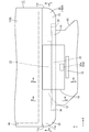
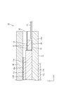
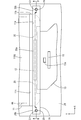
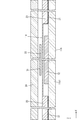
- the top view of the liquid crystal panel which concerns on Embodiment 1 of this invention Plan view of touch panel pattern arranged on the display surface of the CF substrate constituting the liquid crystal panel
- Bottom view of spacer member The top view which shows the state which set the liquid crystal panel and the spacer member to the jig DD sectional view of FIG. Sectional drawing which cut
- FIGS. 1 A first embodiment of the present invention will be described with reference to FIGS.
- a liquid crystal display device 10 having a touch panel function (position input function) in addition to the display function will be described.
- a part of each drawing shows an X axis, a Y axis, and a Z axis, and each axis direction is drawn to be a direction shown in each drawing.
- FIGS. 4 to 6 and 9 are used as a reference, and the upper side of the figure is the front side and the lower side of the figure is the back side.
- the liquid crystal display device 10 has a substantially vertically long rectangular shape as a whole, and includes a display surface 11DS capable of displaying an image on the front plate surface (display panel, with position input function).
- the liquid crystal display device 10 according to the present embodiment is used in a portable information terminal such as a smartphone, for example, and the screen size of the liquid crystal panel 11 is generally classified as small (for example, about several inches). It is said that.
- the liquid crystal panel 11 is a pair of substrates 11 a and 11 b that are almost transparent and made of glass, for example, and are bonded to each other with their inner surfaces facing each other with a predetermined gap (cell gap) therebetween. And a liquid crystal layer (not shown) sealed between the substrates 11a and 11b.
- the CF substrate (first substrate, counter substrate) 11a arranged on the front side has a predetermined arrangement of colored portions such as R (red), G (green), and B (blue).
- a structure such as an alignment film is provided.
- the array substrate (second substrate, active matrix substrate) 11b arranged on the back side has switching elements (for example, TFTs) connected to mutually orthogonal source lines and gate lines, and pixels connected to the switching elements. Structures such as electrodes and alignment films are provided.
- a pair of front and back polarizing plates 11c are attached to the outer surfaces of the pair of substrates 11a and 11b, respectively. The surface of the polarizing plate 11c attached to the front side of the CF substrate 11a constitutes the display surface 11DS.
- the display surface 11DS of the liquid crystal panel 11 has a display area (active area) AA on which an image is displayed and a frame shape (frame shape) surrounding the display area AA, and no image is displayed. It is divided into areas (non-active areas) NAA.
- the alternate long and short dash line represents the outer shape of the display area AA, and the area outside the alternate long and short dash line is the non-display area NAA.
- the CF substrate 11a constituting the liquid crystal panel 11 has a long side dimension shorter than the long side dimension of the array substrate 11b, whereas one end in the long side direction is aligned with the array substrate 11b. It is pasted together.
- the other end of the array substrate 11b in the long side direction is a CF substrate non-overlapping portion 11b1 that protrudes laterally with respect to the CF substrate 11a and does not overlap with the CF substrate 11a.
- the CF substrate non-overlapping portion 11b1 is a non-display area NAA.
- the CF substrate non-overlapping portion 11b1 has a display driver (drive circuit portion, panel drive portion) 12 mounted thereon, and an array having a function of transmitting a signal related to a display function to the driver 12.
- a flexible substrate for substrate (second substrate connecting member) 13 is connected.
- the driver 12 and the array substrate flexible substrate 13 are arranged so as to overlap the front side (the same side as the CF substrate 11a) with respect to the CF substrate non-overlapping portion 11b1 in the Z-axis direction.
- a CF substrate flexible substrate (first substrate connecting member) 14 for transmitting signals related to the touch panel function is connected to the end on the CF substrate non-overlapping portion 11b1 side of the outer peripheral end of the CF substrate 11a.
- the CF substrate flexible substrate 14 is arranged on the front side with respect to the CF substrate 11a in the Z-axis direction.
- the driver 12 is composed of an LSI chip having a drive circuit therein, and is connected to the CF substrate non-overlapping portion 11b1 of the array substrate 11b through COF (Chip On Glass) via an ACF (Anisotropic Conductive Film).
- COF Chip On Glass
- ACF Anaisotropic Conductive Film
- the driver 12 is disposed at a position closer to the CF substrate 11a with respect to the array substrate flexible substrate 13 in the Y-axis direction (alignment direction of the driver 12 and the array substrate flexible substrate 13) in the CF substrate non-overlapping portion 11b1. In the X-axis direction, it is arranged at a substantially central position.
- the driver 12 processes various signals transmitted by the array substrate flexible substrate 13 to generate an output signal, and outputs the output signal to the display area AA of the array substrate 11b.
- each of the array substrate flexible substrate 13 and the CF substrate flexible substrate 14 has flexibility by including a film-like base material made of a synthetic resin material (for example, polyimide resin).
- the substrate has a large number of wiring patterns and a large number of terminal portions (none of which are shown). Terminal portions (not shown) connected to the respective terminal portions of the flexible substrate 13 for the array substrate and the flexible substrate 14 for the CF substrate are provided at each end of the CF substrate a and the array substrate 11b. The parts are electrically connected via the ACF.
- the array substrate flexible substrate 13 has one end side closer to the end in the Y-axis direction with respect to the driver 12 in the CF substrate non-overlapping portion 11b1 of the array substrate 11b (the opposite side to the CF substrate 11a side).
- the other end is connected to a control board (not shown) as a signal supply source, and signals relating to image display supplied from the control board are transmitted to the array board 11b.
- the array substrate flexible substrate 13 includes a power supply connector portion 13a that can be connected to the CF substrate flexible substrate 14, a touch driver (position detection drive circuit portion) 15 that processes a signal related to position detection, and the like.
- the output signal obtained by processing the signal related to position detection supplied from the control board by the touch driver 15 can be transmitted to the flexible board 14 for CF board.
- the flexible substrate 13 for the array substrate has a dimension in the X-axis direction larger than the same dimension of the driver 12.
- the CF substrate flexible substrate 14 is connected at one end to the end on the driver 12 side in the Y-axis direction of the CF substrate 11a, while the other end is flexible as described above.
- the signal is connected to the power supply connector portion 13a of the substrate 13, and a signal supplied from the control substrate and processed by the touch driver 15 of the array substrate flexible substrate 13 can be transmitted to the CF substrate 11a.
- a power receiving connector portion 14a fitted and connected to the power supply connector portion 13a is provided on the other end side of the CF substrate flexible substrate 14.
- One end of the CF substrate flexible substrate 14 is connected to the center position in the X-axis direction with respect to the end portion of the CF substrate 11a, and the dimension in the X-axis direction is smaller than the same dimension of the driver 12.
- the Accordingly, the CF substrate flexible substrate 14 is partially overlapped with each of the driver 12 and the array substrate flexible substrate 13 in plan view, and between the CF substrate non-overlapping portion 11b1 of the array substrate 11b. The arrangement is such that most of the driver 12 and one end side of the array substrate flexible substrate 13 are sandwiched.
- the cover glass 24 has a vertically long and substantially rectangular shape so as to cover the liquid crystal panel 11 from the front side over almost the entire region, thereby protecting both the substrates 11 a and 11 b constituting the liquid crystal panel 11. Can be planned.
- the cover glass 24 is arranged so as to face the CF substrate 11a on the opposite side to the array substrate 11b side, and is at least the driver 12, the array substrate flexible substrate 13 and the CF substrate between the CF substrate non-overlapping portion 11b1.
- the flexible substrate 14 for use is disposed in a sandwiched manner.
- the cover glass 24 is fixed to the front-side polarizing plate 11c via a substantially transparent fixing tape 24a, and a predetermined amount in the Z-axis direction is provided between the cover glass 24 and the CF substrate flexible substrate 14 disposed opposite to the back side. It is assumed that there is a gap.
- the cover glass 24 is made of glass that is substantially transparent and has excellent translucency and has a plate shape, and is preferably made of tempered glass.
- the liquid crystal panel 11 has a display function for displaying an image and a touch panel function (position input function) for detecting a position (input position) input by a user based on the displayed image.
- the touch panel pattern for exhibiting the touch panel function is integrated (semi-in-cell).
- This touch panel pattern is a so-called projected capacitance method, and its detection method is a mutual capacitance method.
- the touch panel pattern is provided on the CF substrate 11a of the pair of substrates 11a and 11b, and a plurality of touch panel patterns arranged in a matrix within the surface of the display surface 11DS on the CF substrate 11a.
- At least a touch electrode (position detection electrode) 16 is provided.
- the touch electrode 16 is disposed in the display area AA of the CF substrate 11a. Therefore, the display area AA in the liquid crystal panel 11 substantially coincides with the touch area where the input position can be detected, and the non-display area NAA substantially coincides with the non-touch area where the input position cannot be detected. Further, the non-display area NAA of the CF substrate 11a, which is a non-touch area outside the touch area, is connected to a terminal portion having one end connected to the touch electrode 16 and the other end connected to the CF board flexible substrate 14. Peripheral wiring 17 is arranged.
- the finger and the touch electrode 16 are placed between the finger and the touch electrode 16. Capacitance is formed. Thereby, the capacitance detected by the touch electrode 16 near the finger changes as the finger approaches and differs from the touch electrode 16 far from the finger. Thus, the input position can be detected.
- the liquid crystal panel 11 includes a spacer member 18 as shown in FIGS.
- the spacer member 18 has a horizontally long shape extending along the X-axis direction as a whole, and is attached so as to overlap almost the entire region of the CF substrate non-overlapping portion 11 b 1 in the liquid crystal panel 11.
- the spacer member 18 is made of a synthetic resin film material 19 having an insulating property, a block material 20 made of an insulating synthetic resin material and fixed to the back side of the film material 19, and a block made of an adhesive material.
- the fixing layer 21 is provided on the back surface of the material 20.
- the film material 19 has a thickness smaller than that of the block material 20 and has substantially the same formation range as the CF substrate non-overlapping portion 11b1 in a plan view.
- the block material 20 has a thickness larger than that of the film material 19 (projection height of the driver 12) and is fixed to both end portions in the long side direction (X-axis direction) of the film material 19 in a pair. Is arranged.
- the fixing layer 21 is disposed over almost the entire area of the block member 20 in a plan view. In FIGS. 5 and 6, the fixed layer 21 is indicated by a thick line.
- the spacer member 18 includes a spacer portion 22 disposed between the driver 12 and the CF substrate flexible substrate 14, and a CF substrate non-overlapping portion 11 b 1. At least a spacer coupling portion 23 that is arranged so as to overlap the front side (the same side as the CF substrate 11a) in the Z-axis direction with respect to a portion that does not overlap with at least the driver 12, and is continuous with the spacer portion 22. Yes.
- the spacer portion 22 is composed of a portion of the film material 19 that does not overlap with the block material 20, and specifically, a central portion of the film material 19 in the length direction.
- the spacer portion 22 is disposed to face the front side with a gap in the Z-axis direction with respect to the CF substrate non-overlapping portion 11b1, sandwiching the driver 12 between the CF substrate non-overlapping portion 11b1 and the driver 12 and CF It is arranged in such a manner that it is sandwiched between the flexible substrate 14 for substrates.
- the spacer portion 22 is disposed so as to face the driver 12 and the CF substrate flexible substrate 14 with a predetermined space therebetween, and is kept in a non-contact state with them. As shown in FIGS.
- the spacer coupling portion 23 has a laminated structure of the block material 20 and a portion of the film material 19 that overlaps the block material 20, and the spacer portion in the X-axis direction. 22 are arranged next to each other. A pair of spacer coupling portions 23 are arranged so as to sandwich the spacer portion 22 on the center side in the X-axis direction (the alignment direction of the spacer portions 22 and the spacer coupling portions 23).
- the spacer coupling portion 23 has a formation range in a plan view that matches the block material 20.
- the film material 19 which comprises the spacer member 18 is extended over the spacer part 22 and a pair of spacer coupling
- the spacer coupling portion 23 is arranged so as to overlap the front side with respect to at least a portion that does not overlap the driver 12 in the CF substrate non-overlapping portion 11 b 1. Therefore, the step between the driver 12 that overlaps with the CF substrate non-overlapping portion 11b1 on the front side and the portion of the CF substrate non-overlapping portion 11b1 that does not overlap with the driver 12 can be reduced. As a result, when an external force (stress) is applied to the CF substrate non-overlapping portion 11b1, it is difficult for stress concentration to occur at a specific location, so that the CF substrate non-overlapping portion 11b1 and the driver 12 mounted thereon are damaged. It will be difficult.
- the spacer coupling portion 23 makes it difficult for stress concentration to occur at a specific location in the CF substrate non-overlapping portion 11b1, the CF substrate non-overlapping portion 11b1 and the driver 12 are less likely to be damaged.
- the spacer coupling portion 23 is configured to be continuous with the spacer portion 22, the number of components is reduced to facilitate component management, and the assembly man-hour is reduced, thereby reducing the manufacturing cost. Is suitable.
- the pair of spacer coupling portions 23 are arranged so as to sandwich the spacer portion 22 in the X-axis direction, stress concentration when stress acts on the CF substrate non-overlapping portion 11b1 can be made less likely to occur. it can. As a result, the CF substrate non-overlapping portion 11b1 and the driver 12 are less likely to be damaged. Furthermore, since the pair of spacer coupling portions 23 are respectively connected to the spacer portion 22 and are made into one part, it is more suitable for reducing the manufacturing cost.
- the spacer coupling portion 23 is arranged in a form that does not overlap with the array substrate flexible substrate 13.
- the block material 20 constituting the spacer coupling portion 23 is located on the end side in the X-axis direction where the arrangement is aligned with the flexible substrate 13 for the array substrate in the Y-axis direction with respect to the portion that is aligned with the driver 12 in the Y-axis direction. It has a planar shape to be retracted, and is prevented from overlapping with the array substrate flexible substrate 13. According to such a configuration, it is possible to avoid a situation where the spacer coupling portion 23 adversely affects the connection state of the array substrate flexible substrate 13 to the CF substrate non-overlapping portion 11b1.
- the spacer coupling portion 23 has a thickness larger than the protrusion height of the driver 12 from the CF substrate non-overlapping portion 11b1.
- the driver 12 mounted on the CF substrate non-overlapping portion 11b1 by the spacer coupling portion 23 and the CF substrate non-superimposing portion 11b1
- the step between the driver 12 and the non-overlapping portion can be more suitably mitigated.
- stress concentration when stress is applied to the CF substrate non-overlapping portion 11b1 can be made less likely to occur, and the CF substrate non-overlapping portion 11b1 and the driver 12 are less likely to be damaged.
- the thickness of the block member 20 constituting the spacer coupling portion 23 is made larger than the protruding height of the driver 12, and the gap is provided between the CF substrate non-overlapping portion 11 b 1 and the spacer portion 22. And are almost equal. As a result, the surface of the spacer coupling portion 23 with respect to the spacer portion 22 (on the side opposite to the CF substrate non-overlapping portion 11b1 side) is flush with each other. According to such a configuration, it is possible to avoid steps and wrinkles due to the flat surfaces of the spacer coupling portion 23 and the spacer portion 22 being flat.
- the spacer member 18 is disposed so as to be interposed between the array substrate flexible substrate 13 and the CF substrate flexible substrate 14, and has an insulating property. It has the 2nd spacer part 25 connected with the coupling
- FIG. The second spacer portion 25 is composed of a portion of the film material 19 that does not overlap with the block material 20, and is specifically a central portion in the length direction of the film material 19 and the Y-axis direction. About the CF substrate 11a side. That is, the second spacer portion 25 is arranged adjacent to the spacer portion 22 on the side opposite to the CF substrate 11a side in the Y-axis direction.
- the second spacer portion 25 is disposed to face the front side with a gap in the Z-axis direction with respect to the CF substrate non-overlapping portion 11b1, and the array substrate flexible substrate 13 is disposed between the second spacer portion 25 and the CF substrate non-overlapping portion 11b1.
- the flexible substrate 13 for the array substrate and the flexible substrate 14 for the CF substrate are disposed so as to be sandwiched.
- the second spacer portion 25 is the CF substrate flexible substrate 14 and the array substrate flexible substrate. 13 is disposed in a form intervening between the two.
- the spacer part 22 when the spacer part 22, the spacer coupling part 23, and the second spacer part 25 that are connected to each other are attached to the CF substrate non-overlapping part 11b1 of the array substrate 11b, for example, the spacer part 22 is in the Y-axis direction with respect to the driver 12 Even when the position is shifted to the CF substrate 11 a side, a part of the insulating second spacer portion 25 is disposed between the driver 12 and the CF substrate flexible substrate 14. become. As described above, even when the spacer portion 22 is displaced in the Y-axis direction with respect to the driver 12, the second spacer portion 25 prevents the CF substrate flexible substrate 14 from being accidentally short-circuited to the driver 12. it can.
- the spacer coupling portion 23 is connected to the spacer portion 22 and the second spacer portion 25 in a linear shape along the X-axis direction.
- the spacer portion 22 and the second spacer portion 25 The stress concentration is less likely to occur at the boundary portion between the spacer portion 25 and the spacer coupling portion 23. Thereby, it becomes difficult to produce a cut
- the spacer coupling portion 23 among the spacer portion 22, the spacer coupling portion 23, and the second spacer portion 25 constituting the spacer member 18 has a fixing layer 21 fixed to the CF substrate non-overlapping portion 11 b 1. It is provided selectively. In FIG. 7, the non-formation range of the fixing layer 21 in the spacer member 18 is shown in a shaded shape.
- the spacer coupling portion 23 is fixed to the CF substrate non-overlapping portion 11b1 by fixing the selectively provided fixing layer 21 to the CF substrate non-overlapping portion 11b1, so that the CF substrate non-overlapping portion 11b1 Stress concentration is less likely to occur.
- the liquid crystal display device 10 of the present embodiment has the above structure, and a method for manufacturing the liquid crystal display device 10 will be described.
- the manufacturing method of the liquid crystal display device 10 includes a liquid crystal panel manufacturing process for manufacturing the liquid crystal panel 11, a backlight device manufacturing process for manufacturing the backlight device, and various components related to the liquid crystal panel 11 including the spacer member 18.
- an assembling step of assembling the backlight device and the cover glass 24 to the liquid crystal panel 11 to which the components are attached is provided.
- the substrate bonding is performed such that the array substrate 11b is bonded to the CF substrate 11a so as to be opposed to each other so that a part of the CF substrate 11a is a non-overlapping CF substrate non-overlapping portion 11b1.
- At least a process is included (see FIG. 4).
- the backlight device manufacturing process and the component manufacturing process are known, but in the spacer manufacturing process included in the component manufacturing process, the film material 19 and the block material 20 that are separately molded are fixed. Then, the spacer member 18 is manufactured, and the separator 26 is detachably attached to the front side of the spacer member 18 (see FIG. 8). As shown in FIG.
- the separator 26 includes a spacer overlapping portion 26 a that overlaps the entire area of the spacer member 18, and a pair of spacers that protrude on both sides of the spacer member 18 in the X-axis direction and that do not overlap the spacer member 18. And a non-overlapping portion 26b.
- a separator-side positioning portion 27 is provided in each of the pair of spacer non-overlapping portions 26b.
- the separator-side positioning portion 27 has a hole shape penetrating the spacer non-overlapping portion 26b in the thickness direction.
- the component mounting process includes a driver mounting process (driving circuit unit mounting process) in which the driver 12 is mounted on the front side of the CF substrate non-overlapping portion 11b1, and a shape of the front side of the CF substrate non-overlapping portion 11b1
- the array substrate flexible substrate connecting step (second substrate connecting member connecting step) for connecting the array substrate flexible substrate 13 and the spacer arrangement in which the spacer member 18 is arranged on the front side with respect to the CF substrate non-overlapping portion 11b1.
- a CF substrate flexible substrate connecting step (first substrate connecting member connecting step) for connecting the CF substrate flexible substrate 14 so as to overlap the end of the CF substrate 11a on the front side (see FIG. 4).
- the driver 12 and the array substrate flexible substrate 13 are mounted on the CF substrate non-overlapping portion 11b1 via the ACF (see FIG. 4).
- the spacer placement step includes a substrate placement step of placing the liquid crystal panel 11 (CF substrate 11a and array substrate 11b) with respect to the jig 28, and a separator mounted on the spacer member 18. And a spacer positioning step for positioning the spacer member 18 with respect to the CF substrate non-overlapping portion 11b1 by using H.26.
- the jig 28 includes a panel positioning portion (not shown) for positioning the liquid crystal panel 11 in the X-axis direction and the Y-axis direction (direction along the display surface 11DS), and a separator 26 mounted on the spacer member 18. At least a jig-side positioning portion 29 for positioning is provided.
- the jig-side positioning portion 29 has a protruding shape that protrudes toward the front side from the support surface of the liquid crystal panel 11 in the jig 28, and a pair is provided on the support surface at positions separated in the X-axis direction. Yes.
- the pair of separator-side positioning portions 27 provided on the spacer non-overlapping portion 26b are moved while the spacer member 18 is brought closer to the CF substrate non-overlapping portion 11b1 from the front side.
- the concave and convex portions are fitted to a pair of jig side positioning portions 29 provided on the jig 28.
- the certainty of arranging the spacer portion 22 so as to overlap the front side of the driver 12, the certainty of arranging the second spacer portion 25 so as to overlap the front side of the array substrate flexible substrate 13, and the spacer coupling portion The reliability of arranging 23 in such a manner as to overlap the driver 12 and the array substrate flexible substrate 13 in the non-overlapping portion of the CF substrate non-overlapping portion 11b1 is high.
- the second spacer portion 25 is arranged so as to overlap the front side, and further, the second spacer portion 25 overlaps the front side with respect to the portion of the CF substrate non-overlapping portion 11b1 that does not overlap with the driver 12 and the array substrate flexible substrate 13.
- the spacer coupling portion 23 is disposed. At this time, in the spacer coupling portion 23, the fixing layer 21 provided on the back side surface is fixed to the CF substrate non-overlapping portion 11b1, whereby the spacer member 18 is fixed.
- the spacer portion 22 and the second spacer portion 25 do not have the fixing layer 21, they can be prevented from sticking to the overlapping driver 12 and the flexible substrate 13 for the array substrate during the attachment, whereby the spacer It is difficult for wrinkles or the like to move to the portion 22 and the second spacer portion 25 and the workability is good.
- the separator 26 is removed from the spacer member 18.
- the CF substrate flexible substrate 14 is disposed so as to partially overlap the driver 12 with respect to the CF substrate 11 a and the spacer portion 22 is sandwiched between the driver 12 and the CF substrate 11 a. Connect as shown (see FIG. 4). Thereafter, the power receiving connector portion 14 a of the CF substrate flexible substrate 14 is fitted and connected to the power feeding connector portion 13 a of the array substrate flexible substrate 13. Thereby, a signal related to position detection transmitted from the control substrate to the array substrate flexible substrate 13 is processed by the touch driver 15, and then supplied to the touch panel pattern of the CF substrate 11a via the CF substrate flexible substrate 14. It becomes possible.
- the liquid crystal display device (display device) 10 of the present embodiment is overlapped with the CF substrate (first substrate) 11a so as to face the CF substrate 11a, and a part thereof does not overlap with the CF substrate 11a.
- the CF substrate non-overlapping portion (first substrate non-overlapping portion) 11b1 and the array substrate (second substrate) 11b are mounted on the same side as the CF substrate 11a with respect to the CF substrate non-overlapping portion 11b1.
- Driver driving circuit unit 12
- CF substrate flexible substrate first substrate connecting member 14 that is connected to the CF substrate 11 a and is partially overlapped with the driver 12
- CF substrate flexible substrate 14 and an insulating spacer 22 arranged between the driver 12 and the driver 12, and at least a portion of the CF substrate non-overlapping portion 11b1 that does not overlap with the driver 12 CF.
- Arranged in the form of overlapping on the same side as the plate 11a includes a spacer coupling portion 23 continuous with the spacer section 22, a.
- the CF substrate non-overlapping portion that does not overlap the CF substrate 11a among the CF substrate flexible substrate 14 connected to the CF substrate 11a and the array substrate 11b that is stacked in a manner facing the CF substrate 11a.
- the CF board flexible substrate 14 is arranged by interposing an insulating spacer 22 between the driver 12 mounted on the same side as the CF substrate 11a with respect to 11b1. Can be prevented from being accidentally short-circuited to the driver 12.
- the spacer coupling portion 23 is arranged on the same side as the CF substrate 11a with respect to at least a portion of the CF substrate non-overlapping portion 11b1 that does not overlap with the driver 12, the CF substrate non-overlapping portion 11b1
- the step between the driver 12 that overlaps the same side as the CF substrate 11a and the portion of the CF substrate non-overlapping portion 11b1 that does not overlap the driver 12 can be reduced.
- stress concentration is less likely to occur at a specific location, so that the CF substrate non-overlapping portion 11b1 and the driver 12 are less likely to be damaged.
- the spacer coupling portion 23 is configured to be continuous with the spacer portion 22, the number of components is reduced to facilitate component management, and the assembly man-hour is reduced, thereby reducing the manufacturing cost. Is suitable.
- a flexible substrate for array substrate (second substrate connecting member) 13 connected to a position opposite to the CF substrate 11a side with respect to the driver 12 in the CF substrate non-overlapping portion 11b1 is provided, and the spacer connection is provided.
- the formation part 23 is arranged in a non-overlapping manner with the array substrate flexible substrate 13. By doing so, it is possible to avoid a situation in which the spacer coupling portion 23 adversely affects the connection state of the array substrate flexible substrate 13 to the CF substrate non-overlapping portion 11b1.
- a second spacer portion which is arranged in a form interposed between the CF substrate flexible substrate 14 and the array substrate flexible substrate 13 and has an insulating property and is connected to the spacer portion 22 and the spacer coupling portion 23. 25.
- the second spacer portion 25 is provided with the CF substrate flexible substrate 14 and the array substrate. They are arranged so as to be interposed between the flexible substrate 13.
- the spacer portion 22 when the spacer portion 22, the spacer coupling portion 23, and the second spacer portion 25 that are connected to each other are attached to the CF substrate non-overlapping portion 11b1 of the array substrate 11b, for example, the spacer portion 22 is connected to the driver 12 with respect to the CF substrate 11a. Even when the position is shifted to the side, a part of the insulating second spacer portion 25 is disposed between the driver 12 and the CF substrate flexible substrate 14. Thus, even when the spacer portion 22 is displaced with respect to the driver 12, it is possible to prevent the second spacer portion 25 from accidentally short-circuiting the CF substrate flexible substrate 14 to the driver 12.
- the spacer coupling portion 23 is connected to the spacer portion 22 and the second spacer portion 25 in a linear shape along the direction in which the spacer portion 22 and the second spacer portion 25 are aligned. In this way, compared to the case where the spacer coupling portion is non-linear along the alignment direction with respect to the spacer portion 22 and the second spacer portion 25 and unevenness is generated at the boundary portion, Stress concentration is unlikely to occur at the boundary portion between the spacer portion 22 and the second spacer portion 25 and the spacer coupling portion 23, and cutting or the like is unlikely to occur at the boundary portion.
- the spacer coupling portion 23 among the spacer portion 22, the spacer coupling portion 23, and the second spacer portion 25 is selectively provided with a fixing layer 21 fixed to the CF substrate non-overlapping portion 11b1.
- the spacer coupling portion 23 is fixed to the CF substrate non-overlapping portion 11b1 by fixing the selectively provided fixing layer 21 to the CF substrate non-overlapping portion 11b1, so that the CF Stress concentration is less likely to occur in the substrate non-overlapping portion 11b1.
- the position of the second spacer portion 25 with respect to 14 can be easily adjusted. Thereby, it is excellent in workability in manufacturing.
- the thickness of the spacer coupling portion 23 is larger than the protruding height of the driver 12 from the CF substrate non-overlapping portion 11b1. In this way, compared to the case where the thickness of the spacer coupling portion is smaller than the protruding height of the driver 12, the driver 12 mounted on the CF substrate non-overlapping portion 11b1 by the spacer coupling portion 23 and the CF substrate non-overlapping The level difference between the non-overlapping portion and the driver 12 in the overlapping portion 11b1 can be more preferably reduced. As a result, stress concentration when stress is applied to the CF substrate non-overlapping portion 11b1 can be made less likely to occur, and the CF substrate non-overlapping portion 11b1 and the driver 12 are less likely to be damaged.
- the spacer coupling portion 23 is flush with the spacer portion 22 on the opposite side of the CF substrate non-overlapping portion 11b1 side. In this way, it is possible to avoid a step on the surface opposite to the CF substrate non-overlapping portion 11b1 side in the spacer coupling portion 23 and the spacer portion 22.
- a pair of spacer coupling portions 23 are arranged in such a manner that the spacer portions 22 are sandwiched in the alignment direction with respect to the spacer portions 22.
- the stress concentration when stress is applied to the CF substrate non-overlapping portion 11b1 by the pair of spacer coupling portions 23 arranged so as to sandwich the spacer portion 22 in the arrangement direction can be made more difficult to occur. Therefore, the CF substrate non-overlapping portion 11b1 and the driver 12 are less likely to be damaged.
- the pair of spacer coupling portions 23 are respectively connected to the spacer portion 22 and are made into one component, it is more suitable for reducing the manufacturing cost.
- a cover that is arranged to face the CF substrate 11a opposite to the array substrate 11b and sandwiches the driver 12, the spacer portion 22 and the CF substrate flexible substrate 14 with the CF substrate non-overlapping portion 11b1.
- a glass (substrate protection member) 24 is provided. In this way, the CF substrate 11a and the array substrate 11b can be protected by the cover glass 24.
- stress tends to be generated in the CF substrate non-overlapping portion 11 b 1, but the CF substrate by the spacer coupling portion 23.
- the array substrate 11b is opposed to the CF substrate 11a so that a part thereof becomes the CF substrate non-overlapping portion 11b1 that does not overlap the CF substrate 11a.
- an insulating spacer portion 22 is disposed so as to overlap with the same side as the CF substrate 11a, and at least a portion of the CF substrate non-overlapping portion 11b1 that does not overlap with the driver 12 is the same as the CF substrate 11a.
- the spacer portion 22 is disposed on the same side as the CF substrate 11a with respect to the driver 12, and the CF A spacer coupling portion 23 connected to the spacer portion 22 is arranged on the same side as the CF substrate 11a with respect to at least a portion that does not overlap the driver 12 in the substrate non-overlapping portion 11b1.
- the spacer coupling portion 23 relaxes the step between the driver 12 mounted on the CF substrate non-overlapping portion 11b1 and the portion of the CF substrate non-overlapping portion 11b1 that does not overlap with the driver 12.
- the CF substrate flexible substrate connecting step when stress is applied to the CF substrate non-overlapping portion 11b1, stress concentration is less likely to occur at a specific location, so that the CF substrate non-overlapping portion 11b1 and the driver 12 are less likely to be damaged.
- the CF substrate flexible substrate connecting step when the CF substrate flexible substrate connecting step is performed, the CF substrate flexible substrate 14 is connected to the CF substrate 11a, and a part of the CF substrate flexible substrate 14 is arranged so as to overlap the driver 12.
- the spacer portion 22 is sandwiched between the driver 12 and the driver 12.
- the spacer coupling portion 23 is configured to be continuous with the spacer portion 22, the number of components is reduced to facilitate component management, and the assembly man-hour is reduced, thereby reducing the manufacturing cost. Is suitable.
- the substrate placement step for placing the CF substrate 11a and the array substrate 11b with respect to the jig 28, and the attachment / detachment on the side opposite to the driver 12 side with respect to the spacer portion 22 and the spacer coupling portion 23.
- Separator 26 that is mounted in a possible manner and has a spacer non-overlapping portion 26b that does not overlap spacer portion 22 and spacer coupling portion 23, and is provided on the separator non-overlapping portion 26b.
- At least a spacer positioning step of positioning the spacer portion 22 and the spacer coupling portion 23 by fitting the positioning portion 27 to the jig-side positioning portion 29 provided on the jig 28 in a concave-convex manner is included.
- the separator-side positioning portion 27 provided on the spacer non-overlapping portion 26b of the separator 26 and the jig
- the spacer portion 22 and the spacer coupling portion 23 mounted in a detachable manner with respect to the separator 26 are formed by the jig-side positioning portion 29 provided on the jig 28 so that the CF plate non-overlapping portion is mounted.
- 11b1 and the driver 12 are positioned. This ensures that the spacer portion 22 is disposed between the CF board flexible substrate 14 and the driver 12, and that the spacer coupling portion 23 is not separated from the driver 12 in the CF substrate non-overlapping portion 11b1.
- the spacer portion 22 and the spacer coupling portion 23 are attached to at least the CF substrate non-overlapping portion 11b1, and then the separator 26 is removed from the spacer portion 22 and the spacer coupling portion 23.
- Embodiment 2 A second embodiment of the present invention will be described with reference to FIG. In this Embodiment 2, what changed the structure of the spacer member 118 is shown. In addition, the overlapping description about the same structure, operation
- the spacer member 118 has a configuration in which the film material 19 and the pair of block materials 20 (see FIG. 6) described in the first embodiment are integrated.
- the spacer member 118 is manufactured by resin molding, for example, by a method such as injection molding, and is made of one kind of material. In this way, in the spacer manufacturing process, it is not necessary to perform the work of fixing the film material 19 and the block material 20 separately molded as in the above-described first embodiment. Excellent in improving the performance.
- the present invention is not limited to the embodiments described with reference to the above description and drawings.
- the following embodiments are also included in the technical scope of the present invention.
- the spacer portion is not limited to the configuration in which the spacer portion is opposed to the back side of the CF substrate flexible substrate, but the spacer portion is opposed to the back surface of the CF substrate flexible substrate. It does not matter.
- the touch driver is provided on the array substrate flexible substrate and the other end of the CF substrate flexible substrate is connected to the array substrate flexible substrate. It may be provided on the substrate flexible substrate, and the other end of the CF substrate flexible substrate may be directly connected to the control substrate. In that case, a touch control board may be prepared separately from the control board, and the other end of the CF board flexible board may be connected to the touch control board.
- the thickness of the spacer coupling portion is larger than the protrusion height of the driver from the CF substrate non-overlapping portion is shown.
- the protrusion height of the driver may be substantially the same, and may be smaller than that.
- spacer portion only one spacer coupling portion is provided. It doesn't matter.
- the spacer portion, the second spacer portion, and the spacer coupling portion are linear along the X-axis direction. However, the spacer portion, the second spacer portion, The spacer coupling portion may be non-linear along the X-axis direction, and irregularities (steps) may be generated at the boundary portion.
- the fixing layer is not formed on the spacer portion and the second spacer portion has been shown. However, either one or both of the spacer portion and the second spacer portion are shown. A fixing layer may be formed.
- the mutual capacitive touch panel pattern is exemplified, but the present invention can also be applied to a self capacitive touch panel pattern.
- the case where the planar shape of the liquid crystal display device is a vertically long square is shown, but other than that, a horizontally long square, a square, or the like may be used, and a circle, an ellipse, a trapezoid, or the like The non-square can be used.
- the specific screen size of the liquid crystal panel and the specific use of the liquid crystal display device can be changed as appropriate.
- the liquid crystal display device including the liquid crystal panel is illustrated, but other types of display panels (PDP (plasma display panel), organic EL panel, EPD (electrophoretic display panel), MEMS (The present invention can also be applied to a display device equipped with a display panel (Micro Electro Mechanical Systems). Among these, when a self-luminous display panel is used, a backlight device is not necessary.
- SYMBOLS 10 Liquid crystal display device (display apparatus), 11a ... CF board
Landscapes
- Physics & Mathematics (AREA)
- Nonlinear Science (AREA)
- General Physics & Mathematics (AREA)
- Mathematical Physics (AREA)
- Chemical & Material Sciences (AREA)
- Crystallography & Structural Chemistry (AREA)
- Optics & Photonics (AREA)
- Engineering & Computer Science (AREA)
- Microelectronics & Electronic Packaging (AREA)
- Theoretical Computer Science (AREA)
- Devices For Indicating Variable Information By Combining Individual Elements (AREA)
- Liquid Crystal (AREA)
Abstract
液晶表示装置10は、CF基板11aと、CF基板11aと対向する形で重ねられて一部がCF基板11aとは非重畳となるCF基板非重畳部11b1とされるアレイ基板11bと、CF基板非重畳部11b1に対してCF基板11aと同じ側に重なる形で実装されるドライバ12と、CF基板11aに接続されて一部がドライバ12と重畳する形で配されるCF基板用フレキシブル基板14と、CF基板用フレキシブル基板14とドライバ12との間に介在する形で配されて絶縁性を有するスペーサ部22と、CF基板非重畳部11b1のうち少なくともドライバ12とは非重畳となる部分に対してCF基板11aと同じ側に重なる形で配されてスペーサ部22に連なるスペーサ連成部23と、を備える。
Description
本発明は、表示装置及び表示装置の製造方法に関する。
従来、集積回路モジュールを備える液晶表示装置の一例として下記特許文献1に記載されたものが知られている。特許文献1に記載された液晶表示装置に備わる集積回路モジュールは、駆動用ICと、駆動用ICを搭載する第1フレキシブル基板と、駆動用ICと、駆動用ICを搭載する第2フレキシブル基板と、第1フレキシブル基板の駆動用ICの側とは逆側に配置された第1放熱部と、駆動用ICの第2フレキシブル基板とは逆側に配置される第2放熱部と、駆動用ICと第2フレキシブル基板との間に配置される放熱板と、を含む。
(発明が解決しようとする課題)
上記した特許文献1は、互いに重なり合う配置となる駆動用ICが温度上昇することを課題としているが、温度上昇以外にも下記の問題が生じるおそれがある。すなわち、液晶表示装置の狭額縁化が進行すると、液晶パネルに対する各フレキシブル基板の接続箇所から駆動用ICまでの距離が短くなる傾向となる。このため、液晶パネルに対して各フレキシブル基板を実装する際に生じる位置ずれに起因して、液晶パネルに対する第2フレキシブル基板の接続部位(端子)が駆動用ICに短絡するおそれがある。それ以外にも、液晶パネルのうち各フレキシブル基板が実装される部分は、素子基板が1枚のみとされているため、当該部分には応力集中に伴う破損が生じ易い傾向にあった。
上記した特許文献1は、互いに重なり合う配置となる駆動用ICが温度上昇することを課題としているが、温度上昇以外にも下記の問題が生じるおそれがある。すなわち、液晶表示装置の狭額縁化が進行すると、液晶パネルに対する各フレキシブル基板の接続箇所から駆動用ICまでの距離が短くなる傾向となる。このため、液晶パネルに対して各フレキシブル基板を実装する際に生じる位置ずれに起因して、液晶パネルに対する第2フレキシブル基板の接続部位(端子)が駆動用ICに短絡するおそれがある。それ以外にも、液晶パネルのうち各フレキシブル基板が実装される部分は、素子基板が1枚のみとされているため、当該部分には応力集中に伴う破損が生じ易い傾向にあった。
本発明は上記のような事情に基づいて完成されたものであって、基板接続部品及び駆動回路部の短絡防止と、駆動回路部及び第1基板非重畳部の損傷防止と、を図ることを目的とする。
(課題を解決するための手段)
本発明の表示装置は、第1基板と、前記第1基板と対向する形で重ねられて一部が前記第1基板とは非重畳となる第1基板非重畳部とされる第2基板と、前記第1基板非重畳部に対して前記第1基板と同じ側に重なる形で実装される駆動回路部と、前記第1基板に接続されて一部が前記駆動回路部と重畳する形で配される第1基板接続部材と、前記第1基板接続部材と前記駆動回路部との間に介在する形で配されて絶縁性を有するスペーサ部と、前記第1基板非重畳部のうち少なくとも前記駆動回路部とは非重畳となる部分に対して前記第1基板と同じ側に重なる形で配されて前記スペーサ部に連なるスペーサ連成部と、を備える。
本発明の表示装置は、第1基板と、前記第1基板と対向する形で重ねられて一部が前記第1基板とは非重畳となる第1基板非重畳部とされる第2基板と、前記第1基板非重畳部に対して前記第1基板と同じ側に重なる形で実装される駆動回路部と、前記第1基板に接続されて一部が前記駆動回路部と重畳する形で配される第1基板接続部材と、前記第1基板接続部材と前記駆動回路部との間に介在する形で配されて絶縁性を有するスペーサ部と、前記第1基板非重畳部のうち少なくとも前記駆動回路部とは非重畳となる部分に対して前記第1基板と同じ側に重なる形で配されて前記スペーサ部に連なるスペーサ連成部と、を備える。
このようにすれば、第1基板に接続される第1基板接続部材と、第1基板と対向する形で重ねられる第2基板のうち第1基板とは非重畳となる第1基板非重畳部に対して第1基板と同じ側に重なる形で実装される駆動回路部と、の間には、絶縁性を有するスペーサ部が介在する形で配されることで、第1基板接続部材が誤って駆動回路部に短絡される事態を防ぐことができる。スペーサ連成部は、第1基板非重畳部のうち少なくとも駆動回路部とは非重畳となる部分に対して第1基板と同じ側に重なる形で配されているので、第1基板非重畳部に対して第1基板と同じ側に重なる駆動回路部と、第1基板非重畳部のうちの駆動回路部とは非重畳となる部分と、の間の段差を緩和することができる。これにより、第1基板非重畳部に応力が作用した場合に特定の箇所に応力集中が生じ難くなるので、第1基板非重畳部及び駆動回路部に損傷などが生じ難いものとなる。その上で、スペーサ連成部は、スペーサ部に連なる構成とされているので、部品点数が削減されて部品管理が容易になるとともに組付工数が削減され、もって製造コストを低下させる上で好適となる。
本発明の表示装置の実施態様として、次の構成が好ましい。
(1)前記第1基板非重畳部のうち前記駆動回路部に対して前記第1基板側とは反対側となる位置に接続される第2基板接続部材を備えており、前記スペーサ連成部は、前記第2基板接続部材とは非重畳となる形で配されている。このようにすれば、スペーサ連成部が第1基板非重畳部に対する第2基板接続部材の接続状態に悪影響を及ぼす事態を回避することができる。
(1)前記第1基板非重畳部のうち前記駆動回路部に対して前記第1基板側とは反対側となる位置に接続される第2基板接続部材を備えており、前記スペーサ連成部は、前記第2基板接続部材とは非重畳となる形で配されている。このようにすれば、スペーサ連成部が第1基板非重畳部に対する第2基板接続部材の接続状態に悪影響を及ぼす事態を回避することができる。
(2)前記第1基板接続部材と前記第2基板接続部材との間に介在する形で配されて絶縁性を有していて前記スペーサ部及び前記スペーサ連成部に連ねられる第2のスペーサ部を備える。このようにすれば、スペーサ部が駆動回路部と第1基板接続部材との間に介在する形で配された状態では、第2のスペーサ部が第1基板接続部材と第2基板接続部材との間に介在する形で配される。ここで、互いに連なるスペーサ部、スペーサ連成部及び第2のスペーサ部を第2基板の第1基板非重畳部に取り付ける際に、例えばスペーサ部が駆動回路部に対して第1基板側に位置ずれした場合であっても、絶縁性を有する第2のスペーサ部の一部が駆動回路部と第1基板接続部材との間に介在する形で配されることになる。このように、駆動回路部に対してスペーサ部が位置ずれした場合でも、第2のスペーサ部によって第1基板接続部材が誤って駆動回路部に短絡される事態を防ぐことができる。
(3)前記スペーサ連成部は、前記スペーサ部及び前記第2のスペーサ部に対して前記スペーサ部及び前記第2のスペーサ部との並び方向に沿って直線状をなす形で連ねられる。このようにすれば、仮にスペーサ部及び第2のスペーサ部に対してスペーサ連成部が上記並び方向に沿って非直線状をなしていてその境界部位に凹凸が生じる場合に比べると、スペーサ部及び第2のスペーサ部とスペーサ連成部との境界部位に応力集中が生じ難くなって当該境界部位に切れなどが生じ難くなる。
(4)前記スペーサ部、前記スペーサ連成部及び前記第2のスペーサ部のうちの前記スペーサ連成部には、前記第1基板非重畳部に固着される固着層が選択的に設けられる。このようにすれば、スペーサ連成部は、選択的に設けられた固着層が第1基板非重畳部に固着されることで、第1基板非重畳部に対する固定が図られるので、第1基板非重畳部に応力集中がより生じ難いものとなる。一方、駆動回路部と第1基板接続部材との間に介在するスペーサ部と、第1基板接続部材と第2基板接続部材との間に介在する第2のスペーサ部と、のいずれにも固着層が設けられていないから、互いに連なるスペーサ部、スペーサ連成部及び第2のスペーサ部を取り付ける際に、駆動回路部に対するスペーサ部の位置や第1基板接続部材に対する第2のスペーサ部の位置を容易に調整することが可能となる。これにより、製造に際しての作業性に優れる。
(5)前記スペーサ連成部は、その厚みが、前記第1基板非重畳部からの前記駆動回路部の突出高さと同一またはそれよりも大きい。このようにすれば、仮にスペーサ連成部の厚みが駆動回路部の突出高さよりも小さい場合に比べると、スペーサ連成部によって第1基板非重畳部に実装された駆動回路部と、第1基板非重畳部のうちの駆動回路部とは非重畳となる部分と、の間の段差をより好適に緩和することができる。これにより、第1基板非重畳部に応力が作用した場合の応力集中をより生じ難くすることができ、第1基板非重畳部及び駆動回路部に損傷などがより生じ難いものとなる。
(6)前記スペーサ連成部は、前記スペーサ部に対して前記第1基板非重畳部側とは反対側の面同士が面一状をなす。このようにすれば、スペーサ連成部及びスペーサ部における第1基板非重畳部側とは反対側の面に段差が生じることが避けられる。
(7)前記スペーサ連成部は、前記スペーサ部に対する並び方向について前記スペーサ部を挟み込む形で一対が配される。このようにすれば、上記並び方向についてスペーサ部を挟み込む形で配される一対のスペーサ連成部によって第1基板非重畳部に応力が作用した場合の応力集中をより生じ難くすることができるので、第1基板非重畳部及び駆動回路部に損傷などがより生じ難いものとなる。しかも、一対のスペーサ連成部がそれぞれスペーサ部に連なる構成とされて一部品化が図られているので、製造コストを低下させる上でより好適となる。
(8)前記第1基板に対して前記第2基板側とは反対側に対向する形で配されて前記第1基板非重畳部との間に前記駆動回路部、前記スペーサ部及び前記第1基板接続部材を挟み込む基板保護部材を備える。このようにすれば、基板保護部材によって第1基板及び第2基板の保護を図ることができる。ここで、仮に基板保護部材と第1基板接続部材との間に隙間が生じた場合には、第1基板非重畳部に応力が生じ易くなる傾向にあるものの、スペーサ連成部によって第1基板非重畳部において特定の箇所に応力集中が生じ難くなっているので、第1基板非重畳部及び駆動回路部に損傷などが生じ難くなっている。
本発明の表示装置の製造方法は、第1基板に対して第2基板を、一部が前記第1基板とは非重畳の第1基板非重畳部となるよう対向する形で重ねる形で貼り合わせる基板貼り合わせ工程と、前記第1基板非重畳部に対して前記第1基板と同じ側に重なる形で駆動回路部を実装する駆動回路部実装工程と、前記駆動回路部に対して前記第1基板と同じ側に重なる形で絶縁性を有するスペーサ部を配するとともに、前記第1基板非重畳部のうち少なくとも前記駆動回路部とは非重畳となる部分に対して前記第1基板と同じ側に重なる形で前記スペーサ部に連なるスペーサ連成部を配するスペーサ配置工程と、前記第1基板に対して第1基板接続部材を、一部が前記駆動回路部と重畳する形で配されるとともに前記駆動回路部との間に前記スペーサ部を挟み込む形で配されるよう接続する第1基板接続部材接続工程と、を少なくとも備える。
このようにすれば、基板貼り合わせ工程及び駆動回路部実装工程を経た後にスペーサ配置工程が行われると、駆動回路部に対してスペーサ部が第1基板と同じ側に重なる形で配されるとともに、第1基板非重畳部のうち少なくとも駆動回路部とは非重畳となる部分に対してスペーサ部に連なるスペーサ連成部が第1基板と同じ側に重なる形で配される。このスペーサ連成部によって第1基板非重畳部に実装された駆動回路部と、第1基板非重畳部のうちの駆動回路部とは非重畳となる部分と、の間の段差が緩和される。これにより、第1基板非重畳部に応力が作用した場合に特定の箇所に応力集中が生じ難くなるので、第1基板非重畳部及び駆動回路部に損傷などが生じ難いものとなる。その後、第1基板接続部材接続工程が行われると、第1基板に対して第1基板接続部材が接続され、第1基板接続部材の一部が駆動回路部と重畳する形で配されるとともに駆動回路部との間にスペーサ部を挟み込む形で配される。このとき、絶縁性を有するスペーサ部は、第1基板接続部材と駆動回路部との間に介在する形で配されるので、第1基板接続部材が誤って駆動回路部に短絡される事態を防ぐことができる。その上で、スペーサ連成部は、スペーサ部に連なる構成とされているので、部品点数が削減されて部品管理が容易になるとともに組付工数が削減され、もって製造コストを低下させる上で好適となる。
本発明の表示装置の製造方法の実施態様として、次の構成が好ましい。
(1)前記スペーサ配置工程には、前記第1基板及び前記第2基板を治具に対して配置する基板配置工程と、前記スペーサ部及び前記スペーサ連成部に対して前記駆動回路部側とは反対側に着脱可能な形で装着されるセパレータであって、前記スペーサ部及び前記スペーサ連成部とは非重畳となるスペーサ非重畳部を有するセパレータにおいて、前記スペーサ非重畳部に設けられたセパレータ側位置決め部を、前記治具に設けられた治具側位置決め部に対して凹凸嵌合させて前記スペーサ部及び前記スペーサ連成部を位置決めするスペーサ位置決め工程と、が少なくとも含まれる。基板配置工程を行って第1基板及び第2基板を治具に配置した後にスペーサ位置決め工程が行われると、セパレータのスペーサ非重畳部に設けられたセパレータ側位置決め部と、治具に設けられた治具側位置決め部と、が凹凸嵌合されることで、セパレータに対して着脱可能な形で装着されたスペーサ部及びスペーサ連成部が第1基板非重畳部及び駆動回路部に対して位置決めされる。これにより、スペーサ部を第1基板接続部材と駆動回路部との間に介在させる形で配する確実性と、スペーサ連成部を第1基板非重畳部のうちの駆動回路部とは非重畳となる部分に重ねる形で配する確実性と、が共に高いものとなる。上記のようにして位置決めを行ったら、スペーサ部及びスペーサ連成部を少なくとも第1基板非重畳部に対して取り付けるようにし、それからセパレータをスペーサ部及びスペーサ連成部から取り外す。
(1)前記スペーサ配置工程には、前記第1基板及び前記第2基板を治具に対して配置する基板配置工程と、前記スペーサ部及び前記スペーサ連成部に対して前記駆動回路部側とは反対側に着脱可能な形で装着されるセパレータであって、前記スペーサ部及び前記スペーサ連成部とは非重畳となるスペーサ非重畳部を有するセパレータにおいて、前記スペーサ非重畳部に設けられたセパレータ側位置決め部を、前記治具に設けられた治具側位置決め部に対して凹凸嵌合させて前記スペーサ部及び前記スペーサ連成部を位置決めするスペーサ位置決め工程と、が少なくとも含まれる。基板配置工程を行って第1基板及び第2基板を治具に配置した後にスペーサ位置決め工程が行われると、セパレータのスペーサ非重畳部に設けられたセパレータ側位置決め部と、治具に設けられた治具側位置決め部と、が凹凸嵌合されることで、セパレータに対して着脱可能な形で装着されたスペーサ部及びスペーサ連成部が第1基板非重畳部及び駆動回路部に対して位置決めされる。これにより、スペーサ部を第1基板接続部材と駆動回路部との間に介在させる形で配する確実性と、スペーサ連成部を第1基板非重畳部のうちの駆動回路部とは非重畳となる部分に重ねる形で配する確実性と、が共に高いものとなる。上記のようにして位置決めを行ったら、スペーサ部及びスペーサ連成部を少なくとも第1基板非重畳部に対して取り付けるようにし、それからセパレータをスペーサ部及びスペーサ連成部から取り外す。
(発明の効果)
本発明によれば、基板接続部品及び駆動回路部の短絡防止と、駆動回路部及び第1基板非重畳部の損傷防止と、を図ることができる。
本発明によれば、基板接続部品及び駆動回路部の短絡防止と、駆動回路部及び第1基板非重畳部の損傷防止と、を図ることができる。
<実施形態1>
本発明の実施形態1を図1から図9によって説明する。本実施形態では、表示機能に加えてタッチパネル機能(位置入力機能)を備えた液晶表示装置10について説明する。なお、各図面の一部にはX軸、Y軸及びZ軸を示しており、各軸方向が各図面で示した方向となるように描かれている。また、上下方向については、図4から図6及び図9を基準とし、且つ同図上側を表側とするとともに同図下側を裏側とする。
本発明の実施形態1を図1から図9によって説明する。本実施形態では、表示機能に加えてタッチパネル機能(位置入力機能)を備えた液晶表示装置10について説明する。なお、各図面の一部にはX軸、Y軸及びZ軸を示しており、各軸方向が各図面で示した方向となるように描かれている。また、上下方向については、図4から図6及び図9を基準とし、且つ同図上側を表側とするとともに同図下側を裏側とする。
まず、液晶表示装置10の構成について説明する。液晶表示装置10は、図1に示すように、全体として縦長な略方形状をなしており、画像を表示可能な表示面11DSを表側の板面に備える液晶パネル(表示パネル、位置入力機能付き表示パネル)11と、液晶パネル11の表示面11DSを表側から覆う形で配されるカバーガラス(基板保護部材)24と、液晶パネル11に表示のための照明光を照射するバックライト装置(図示せず)と、を少なくとも備える。本実施形態に係る液晶表示装置10は、例えばスマートフォンなどの携帯型情報端末に用いられるものであり、液晶パネル11の画面サイズが一般的には小型に分類される大きさ(例えば数インチ程度)とされている。
液晶パネル11は、図4に示すように、ほぼ透明で例えばガラス製とされて所定の間隔(セルギャップ)を隔てた状態で互いに内面同士が対向する形で貼り合わせられる一対の基板11a,11bと、両基板11a,11b間に封入される液晶層(図示せず)と、を少なくとも備える。一対の基板11a,11bのうち、表側に配されるCF基板(第1基板、対向基板)11aには、R(赤色),G(緑色),B(青色)等の各着色部が所定配列で配置されたカラーフィルタと、隣り合う着色部の間を仕切る遮光部(ブラックマトリクス)と、が設けられているのに加えて、配向膜等の構造物が設けられている。一方、裏側に配されるアレイ基板(第2基板、アクティブマトリクス基板)11bには、互いに直交するソース配線とゲート配線とに接続されたスイッチング素子(例えばTFT)、そのスイッチング素子に接続された画素電極、配向膜等の構造物が設けられている。一対の基板11a,11bのうちの外面側には、表裏一対の偏光板11cがそれぞれ貼り付けられている。CF基板11aにおいて表側に貼り付けられた偏光板11cの表面が表示面11DSを構成している。
液晶パネル11における表示面11DSは、図1に示すように、画像が表示される表示領域(アクティブエリア)AAと、表示領域AAを取り囲む額縁状(枠状)をなすとともに画像が表示されない非表示領域(ノンアクティブエリア)NAAと、に区分される。なお、図1では、一点鎖線が表示領域AAの外形を表しており、当該一点鎖線よりも外側の領域が非表示領域NAAとなっている。液晶パネル11を構成するCF基板11aは、その長辺寸法がアレイ基板11bの長辺寸法よりも短くされるのに対し、アレイ基板11bに対して長辺方向についての一方の端部が揃う形で貼り合わせられている。従って、アレイ基板11bにおける長辺方向についての他方の端部は、CF基板11aに対して側方に突き出すとともにCF基板11aとは非重畳となるCF基板非重畳部11b1とされる。CF基板非重畳部11b1は、非表示領域NAAである。CF基板非重畳部11b1には、表示用のドライバ(駆動回路部、パネル駆動部)12が実装されているのに加えて、ドライバ12に表示機能に係る信号を伝送するなどの機能を有するアレイ基板用フレキシブル基板(第2基板接続部材)13が接続されている。ドライバ12及びアレイ基板用フレキシブル基板13は、Z軸方向についてCF基板非重畳部11b1に対して表側(CF基板11aと同じ側)に重なる形で配される。一方、CF基板11aの外周端部のうちのCF基板非重畳部11b1側の端部には、タッチパネル機能に係る信号を伝送するためのCF基板用フレキシブル基板(第1基板接続部材)14が接続されている。CF基板用フレキシブル基板14は、Z軸方向についてCF基板11aに対して表側に重なる形で配される。
ドライバ12は、図3に示すように、内部に駆動回路を有するLSIチップからなり、アレイ基板11bのCF基板非重畳部11b1に対してACF(Anisotropic Conductive Film)を介してCOG(Chip On Glass)実装されている。ドライバ12は、CF基板非重畳部11b1においてY軸方向(ドライバ12とアレイ基板用フレキシブル基板13との並び方向)についてアレイ基板用フレキシブル基板13に対してCF基板11a寄りの位置に配されるとともに、X軸方向についてほぼ中央位置に配されている。ドライバ12は、アレイ基板用フレキシブル基板13によって伝送される各種信号を処理して出力信号を生成し、その出力信号をアレイ基板11bの表示領域AAへと出力するものとされる。
アレイ基板用フレキシブル基板13及びCF基板用フレキシブル基板14は、図3に示すように、それぞれ合成樹脂材料(例えばポリイミド系樹脂等)からなるフィルム状の基材を備えることで可撓性を有しており、その基材上に多数本の配線パターン及び多数の端子部(いずれも図示せず)を有している。CF基板a及びアレイ基板11bの各端部には、アレイ基板用フレキシブル基板13及びCF基板用フレキシブル基板14の各端子部に接続される端子部(図示せず)がそれぞれ設けられており、端子部間がACFを介して電気的に接続される。
アレイ基板用フレキシブル基板13は、図3に示すように、一端側がアレイ基板11bのCF基板非重畳部11b1のうちのドライバ12に対してY軸方向について端寄り(CF基板11a側とは反対側)の位置に接続されるのに対し、他端側が信号供給源であるコントロール基板(図示せず)に接続されており、コントロール基板から供給される画像表示に係る信号などをアレイ基板11bに伝送することが可能とされる。さらには、アレイ基板用フレキシブル基板13は、CF基板用フレキシブル基板14に対して接続可能な給電コネクタ部13aと、位置検出に係る信号などを処理するタッチドライバ(位置検出駆動回路部)15と、を有しており、コントロール基板から供給される位置検出に係る信号などをタッチドライバ15にて処理して得られた出力信号をCF基板用フレキシブル基板14に伝送することが可能とされる。アレイ基板用フレキシブル基板13は、X軸方向についての寸法がドライバ12の同寸法よりも大きなものとされる。
CF基板用フレキシブル基板14は、図3に示すように、一端側がCF基板11aのうちのY軸方向についてドライバ12側の端部に接続されるのに対し、他端側が上記したアレイ基板用フレキシブル基板13の給電コネクタ部13aに接続されており、コントロール基板から供給されてアレイ基板用フレキシブル基板13のタッチドライバ15にて処理された信号などをCF基板11aに伝送することが可能とされる。CF基板用フレキシブル基板14の他端側には、給電コネクタ部13aに対して嵌合接続される受電コネクタ部14aが設けられている。CF基板用フレキシブル基板14は、一端側がCF基板11aの端部に対してX軸方向についてほぼ中央位置に接続されており、X軸方向についての寸法がドライバ12の同寸法よりも小さなものとされる。従って、CF基板用フレキシブル基板14は、その一部ずつがドライバ12及びアレイ基板用フレキシブル基板13のそれぞれと平面に視て重畳しており、アレイ基板11bのCF基板非重畳部11b1との間でドライバ12の大部分とアレイ基板用フレキシブル基板13の一端側とをそれぞれ挟み込む配置とされる。
カバーガラス24は、図4に示すように、液晶パネル11を表側からそのほぼ全域にわたって覆うよう縦長の略方形状をなしており、それにより液晶パネル11を構成する両基板11a,11bの保護を図ることができる。カバーガラス24は、CF基板11aに対してアレイ基板11b側とは反対側に対向する形で配されてCF基板非重畳部11b1との間に少なくともドライバ12、アレイ基板用フレキシブル基板13及びCF基板用フレキシブル基板14を挟み込む形で配される。カバーガラス24は、表側の偏光板11cに対してほぼ透明な固定テープ24aを介して固定されており、その裏側に対向配置されたCF基板用フレキシブル基板14との間にZ軸方向について所定の隙間を空けた状態とされる。カバーガラス24は、ほぼ透明で優れた透光性を有するガラス製で板状をなしており、好ましくは強化ガラスからなる。カバーガラス24に用いられる強化ガラスとしては、例えば板状のガラス基材の表面に化学強化処理が施されることで、表面に化学強化層を備えた化学強化ガラスを用いることが好ましいが必ずしもその限りではない。
本実施形態に係る液晶パネル11は、既述した通り、画像を表示する表示機能と、表示される画像に基づいて使用者が入力する位置(入力位置)を検出するタッチパネル機能(位置入力機能)と、を併有しており、このうちのタッチパネル機能を発揮するためのタッチパネルパターンを一体化(セミインセル化)している。このタッチパネルパターンは、いわゆる投影型静電容量方式とされており、その検出方式が相互容量方式とされる。タッチパネルパターンは、図2に示すように、一対の基板11a,11bのうちのCF基板11aに設けられており、CF基板11aにおいて表示面11DSの面内にマトリクス状に並んで配される複数のタッチ電極(位置検出電極)16を少なくとも備える。タッチ電極16は、CF基板11aの表示領域AAに配されている。従って、液晶パネル11における表示領域AAは、入力位置を検出可能なタッチ領域とほぼ一致しており、非表示領域NAAが入力位置を検出不能な非タッチ領域とほぼ一致していることになる。また、タッチ領域の外側の非タッチ領域であるCF基板11aの非表示領域NAAには、一端側がタッチ電極16に、他端側がCF基板用フレキシブル基板14に接続された端子部に、それぞれ接続される周辺配線17が配されている。そして、使用者が視認する表示領域AAの画像に基づいて位置入力をしようとして表示面11DSに導電体である図示しない指(位置入力体)を近づけると、その指とタッチ電極16との間で静電容量が形成されることになる。これにより、指の近くにあるタッチ電極16にて検出される静電容量には指が近づくのに伴って変化が生じ、指から遠くにあるタッチ電極16とは異なるものとなるので、それに基づいて入力位置を検出することが可能となる。
さて、本実施形態に係る液晶パネル11は、図3から図6に示すように、スペーサ部材18を備えている。スペーサ部材18は、全体としてX軸方向に沿って延在する横長形状をなしており、液晶パネル11のうちのCF基板非重畳部11b1のほぼ全域に対して重畳する形で取り付けられている。スペーサ部材18は、絶縁性を有する合成樹脂製のフィルム材19と、絶縁性を有する合成樹脂製とされていてフィルム材19に対して裏側に固定されるブロック材20と、粘着材料からなりブロック材20における裏側の面に設けられる固着層21と、から構成されている。フィルム材19は、厚みがブロック材20よりも小さくされていて、平面に視てCF基板非重畳部11b1とほぼ同じ形成範囲を有している。ブロック材20は、厚みがフィルム材19(ドライバ12の突出高さ)よりも大きくされていて、フィルム材19における長辺方向(X軸方向)についての両端側部分にそれぞれ固定される形で一対が配される。固着層21は、平面に視てブロック材20のほぼ全域にわたって配される。なお、図5及び図6では、固着層21を太線により図示している。
そして、スペーサ部材18は、図3から図6に示すように、ドライバ12とCF基板用フレキシブル基板14との間に介在する形で配されるスペーサ部22と、CF基板非重畳部11b1のうち少なくともドライバ12とは非重畳となる部分に対してZ軸方向について表側(CF基板11aと同じ側)に重なる形で配されてスペーサ部22に連なるスペーサ連成部23と、を少なくとも有している。スペーサ部22は、図4及び図6に示すように、フィルム材19のうちブロック材20とは非重畳となる部分からなり、具体的にはフィルム材19のうち長さ方向についての中央側部分であって且つY軸方向についてCF基板11a側の部分からなる。スペーサ部22は、CF基板非重畳部11b1に対してZ軸方向について間隔を空けて表側に対向配置されており、CF基板非重畳部11b1との間にドライバ12を挟み込むとともに、ドライバ12とCF基板用フレキシブル基板14との間に挟み込まれる形で配される。スペーサ部22は、ドライバ12及びCF基板用フレキシブル基板14との間にそれぞれ所定の間隔を空けて対向配置されていてこれらとは非接触状態に保たれている。スペーサ連成部23は、図5及び図6に示すように、ブロック材20と、フィルム材19のうちブロック材20と重畳する部分と、の積層構造とされており、X軸方向についてスペーサ部22と隣り合う形で並んで配されている。スペーサ連成部23は、X軸方向(スペーサ部22とスペーサ連成部23との並び方向)について中央側のスペーサ部22を挟み込む形で一対が配されている。スペーサ連成部23は、平面に視た形成範囲がブロック材20と一致している。また、スペーサ部材18を構成するフィルム材19は、スペーサ部22及び一対のスペーサ連成部23に跨る形で延在していてこれらを相互に連ねる機能を有している、と言える。
以上の構成によれば、CF基板11aに接続されるCF基板用フレキシブル基板14と、アレイ基板11bのCF基板非重畳部11b1に対して表側に重なる形で実装されるドライバ12と、の間には、図4及び図6に示すように、絶縁性を有するスペーサ部22が介在する形で配されるので、例えばCF基板11aに対してCF基板用フレキシブル基板14の実装位置が正規の位置からY軸方向についてずれてしまい、CF基板用フレキシブル基板14の端子部が部分的にドライバ12と重畳する配置となった場合であっても、CF基板用フレキシブル基板14の端子部が誤ってドライバ12に短絡される事態を防ぐことができる。その一方で、スペーサ連成部23は、図5及び図6に示すように、CF基板非重畳部11b1のうち少なくともドライバ12とは非重畳となる部分に対して表側に重なる形で配されているので、CF基板非重畳部11b1に対して表側に重なるドライバ12と、CF基板非重畳部11b1のうちのドライバ12とは非重畳となる部分と、の間の段差を緩和することができる。これにより、CF基板非重畳部11b1に外力(応力)が作用した場合に特定の箇所に応力集中が生じ難くなるので、CF基板非重畳部11b1及びそこに実装されたドライバ12に損傷などが生じ難いものとなる。特に、本実施形態では、カバーガラス24とCF基板用フレキシブル基板14との間に隙間が空けられているため、CF基板非重畳部11b1に応力が生じ易くなる傾向にあるものの、上記のようにスペーサ連成部23によってCF基板非重畳部11b1において特定の箇所に応力集中が生じ難くなっているので、CF基板非重畳部11b1及びドライバ12に損傷などが生じ難くなっている。その上で、スペーサ連成部23は、スペーサ部22に連なる構成とされているので、部品点数が削減されて部品管理が容易になるとともに組付工数が削減され、もって製造コストを低下させる上で好適となる。しかも、スペーサ連成部23は、X軸方向についてスペーサ部22を挟み込む形で一対が配されているので、CF基板非重畳部11b1に応力が作用した場合の応力集中をより生じ難くすることができる。これにより、CF基板非重畳部11b1及びドライバ12に損傷などがより生じ難いものとなる。さらには、一対のスペーサ連成部23がそれぞれスペーサ部22に連なる構成とされて一部品化が図られているので、製造コストを低下させる上でより好適となる。
スペーサ連成部23は、図3及び図5に示すように、アレイ基板用フレキシブル基板13とは非重畳となる形で配されている。スペーサ連成部23を構成するブロック材20は、Y軸方向についてドライバ12と配置が揃う部分に対してY軸方向についてアレイ基板用フレキシブル基板13と配置が揃う部分がX軸方向について端側に引っ込む平面形状を有しており、アレイ基板用フレキシブル基板13との重畳が避けられている。このような構成によれば、スペーサ連成部23がCF基板非重畳部11b1に対するアレイ基板用フレキシブル基板13の接続状態に悪影響を及ぼす事態を回避することができる。
スペーサ連成部23は、図6に示すように、その厚みがCF基板非重畳部11b1からのドライバ12の突出高さよりも大きくなっている。仮にスペーサ連成部の厚みがドライバ12の突出高さよりも小さい場合に比べると、スペーサ連成部23によってCF基板非重畳部11b1に実装されたドライバ12と、CF基板非重畳部11b1のうちのドライバ12とは非重畳となる部分と、の間の段差をより好適に緩和することができる。これにより、CF基板非重畳部11b1に応力が作用した場合の応力集中をより生じ難くすることができ、CF基板非重畳部11b1及びドライバ12に損傷などがより生じ難いものとなる。その上で、スペーサ連成部23を構成するブロック材20は、その厚みがドライバ12の突出高さよりも大きくされるとともに、CF基板非重畳部11b1とスペーサ部22との間に空けられた間隔とほぼ等しくされている。これにより、スペーサ連成部23は、スペーサ部22に対して表側(CF基板非重畳部11b1側とは反対側)の面同士が面一状をなしている。このような構成によれば、スペーサ連成部23及びスペーサ部22における表側の面がフラットになっていて段差や皺が生じることが避けられる。
スペーサ部材18は、図4に示すように、アレイ基板用フレキシブル基板13とCF基板用フレキシブル基板14との間に介在する形で配されるとともに、絶縁性を有していてスペーサ部22及びスペーサ連成部23に連ねられる第2のスペーサ部25を有する。第2のスペーサ部25は、フィルム材19のうちブロック材20とは非重畳となる部分からなり、具体的にはフィルム材19のうち長さ方向についての中央側部分であって且つY軸方向についてCF基板11a側とは反対側の部分からなる。つまり、第2のスペーサ部25は、スペーサ部22に対してY軸方向についてCF基板11a側とは反対側に隣り合う形で配されている。第2のスペーサ部25は、CF基板非重畳部11b1に対してZ軸方向について間隔を空けて表側に対向配置されており、CF基板非重畳部11b1との間にアレイ基板用フレキシブル基板13を挟み込むとともに、アレイ基板用フレキシブル基板13とCF基板用フレキシブル基板14との間に挟み込まれる形で配される。このように、スペーサ部22がドライバ12とCF基板用フレキシブル基板14との間に介在する形で配された状態では、第2のスペーサ部25がCF基板用フレキシブル基板14とアレイ基板用フレキシブル基板13との間に介在する形で配される。ここで、互いに連なるスペーサ部22、スペーサ連成部23及び第2のスペーサ部25をアレイ基板11bのCF基板非重畳部11b1に取り付ける際に、例えばスペーサ部22がドライバ12に対してY軸方向についてCF基板11a側に位置ずれした場合であっても、絶縁性を有する第2のスペーサ部25の一部がドライバ12とCF基板用フレキシブル基板14との間に介在する形で配されることになる。このように、ドライバ12に対してスペーサ部22がY軸方向について位置ずれした場合でも、第2のスペーサ部25によってCF基板用フレキシブル基板14が誤ってドライバ12に短絡される事態を防ぐことができる。
しかも、スペーサ連成部23は、図7に示すように、スペーサ部22及び第2のスペーサ部25に対してX軸方向に沿って直線状をなす形で連ねられているから、仮にスペーサ部22及び第2のスペーサ部25に対してスペーサ連成部がX軸方向に沿って非直線状をなしていてその境界部位に凹凸(段差)が生じる場合に比べると、スペーサ部22及び第2のスペーサ部25とスペーサ連成部23との境界部位に応力集中が生じ難くなる。これにより、スペーサ部22及び第2のスペーサ部25とスペーサ連成部23との境界部位に切れなどが生じ難くなる。さらには、スペーサ部材18を構成するスペーサ部22、スペーサ連成部23及び第2のスペーサ部25のうちのスペーサ連成部23には、CF基板非重畳部11b1に固着される固着層21が選択的に設けられている。なお、図7では、スペーサ部材18における固着層21の非形成範囲を網掛け状にして図示している。スペーサ連成部23は、選択的に設けられた固着層21がCF基板非重畳部11b1に固着されることで、CF基板非重畳部11b1に対する固定が図られるので、CF基板非重畳部11b1に応力集中がより生じ難いものとなる。一方、ドライバ12とCF基板用フレキシブル基板14との間に介在するスペーサ部22と、CF基板用フレキシブル基板14とアレイ基板用フレキシブル基板13との間に介在する第2のスペーサ部25と、のいずれにも固着層21が設けられていないから、互いに連なるスペーサ部22、スペーサ連成部23及び第2のスペーサ部25を取り付ける際に、ドライバ12に対するスペーサ部22の位置やCF基板用フレキシブル基板14に対する第2のスペーサ部25の位置を容易に調整することが可能となる。これにより、製造に際しての作業性に優れる。
本実施形態の液晶表示装置10は以上のような構造であり、続いて液晶表示装置10の製造方法を説明する。液晶表示装置10の製造方法には、液晶パネル11を製造する液晶パネル製造工程と、バックライト装置を製造するバックライト装置製造工程と、スペーサ部材18を始めとする液晶パネル11に係る各種部品を製造する部品製造工程(スペーサ製造工程)と、液晶パネル製造工程を経て製造された液晶パネル11に対して部品製造工程を経て製造された各種部品を取り付ける部品取付工程と、部品取付工程を経て各種部品が取り付けられた液晶パネル11に対してバックライト装置及びカバーガラス24を組み付ける組み付け工程と、が少なくとも含まれる。
液晶パネル製造工程には、CF基板11aに対してアレイ基板11bを、一部がCF基板11aとは非重畳のCF基板非重畳部11b1となるよう対向する形で重ねる形で貼り合わせる基板貼り合わせ工程が少なくとも含まれる(図4を参照)。バックライト装置製造工程及び部品製造工程は、既知の通りであるが、このうちの部品製造工程に含まれるスペーサ製造工程では、別々に樹脂成形されたフィルム材19とブロック材20とを固定することでスペーサ部材18を製造し、さらにスペーサ部材18に対して表側にセパレータ26を着脱可能な形で装着している(図8を参照)。セパレータ26は、図8に示すように、スペーサ部材18の全域と重畳するスペーサ重畳部26aと、X軸方向についてスペーサ部材18の両側に突出してスペーサ部材18とは非重畳とされる一対のスペーサ非重畳部26bと、を有している。このうちの一対のスペーサ非重畳部26bには、それぞれセパレータ側位置決め部27が設けられている。セパレータ側位置決め部27は、スペーサ非重畳部26bを厚さ方向に貫通する孔状をなしている。部品取付工程には、CF基板非重畳部11b1に対して表側に重なる形でドライバ12を実装するドライバ実装工程(駆動回路部実装工程)と、CF基板非重畳部11b1に対して表側に重なる形でアレイ基板用フレキシブル基板13を接続するアレイ基板用フレキシブル基板接続工程(第2基板接続部材接続工程)と、CF基板非重畳部11b1に対して表側に重なる形でスペーサ部材18を配するスペーサ配置工程と、CF基板11aの端部に対して表側に重なる形でCF基板用フレキシブル基板14を接続するCF基板用フレキシブル基板接続工程(第1基板接続部材接続工程)と、が少なくとも含まれる(図4を参照)。
部品取付工程に含まれるドライバ実装工程及びアレイ基板用フレキシブル基板接続工程では、ドライバ12及びアレイ基板用フレキシブル基板13をCF基板非重畳部11b1に対してACFを介して実装する(図4を参照)。スペーサ配置工程には、図8及び図9に示すように、液晶パネル11(CF基板11a及びアレイ基板11b)を治具28に対して配置する基板配置工程と、スペーサ部材18に装着されたセパレータ26を利用してスペーサ部材18をCF基板非重畳部11b1に対して位置決めするためのスペーサ位置決め工程と、が少なくとも含まれる。治具28には、液晶パネル11をX軸方向及びY軸方向(表示面11DSに沿う方向)について位置決めするためのパネル位置決め部(図示せず)と、スペーサ部材18に装着されたセパレータ26を位置決めするための治具側位置決め部29と、が少なくとも設けられている。治具側位置決め部29は、治具28における液晶パネル11の支持面から表側に向けて突出する突起状をなしており、同支持面上においてX軸方向について離間した位置に一対が設けられている。
スペーサ位置決め工程では、図8及び図9に示すように、スペーサ部材18をCF基板非重畳部11b1に対して表側から近づけつつ、スペーサ非重畳部26bに設けられた一対のセパレータ側位置決め部27を、治具28に設けられた一対の治具側位置決め部29に対して凹凸嵌合させる。これにより、スペーサ部材18を構成するスペーサ部22がドライバ12と重畳し、第2のスペーサ部25がアレイ基板用フレキシブル基板13と重畳し、さらにはスペーサ連成部23がドライバ12及びアレイ基板用フレキシブル基板13とは非重畳となるよう位置決めが図られる。これにより、スペーサ部22をドライバ12の表側に重なる形で配する確実性と、第2のスペーサ部25をアレイ基板用フレキシブル基板13の表側に重なる形で配する確実性と、スペーサ連成部23をCF基板非重畳部11b1のうちのドライバ12及びアレイ基板用フレキシブル基板13とは非重畳となる部分の表側に重なる形で配する確実性と、がいずれも高いものとなる。このようにして位置決めされたスペーサ部材18をCF基板非重畳部11b1に対して取り付けると、ドライバ12に対して表側に重なる形でスペーサ部22が配されるとともに、アレイ基板用フレキシブル基板13に対して表側に重なる形で第2のスペーサ部25が配され、さらには、CF基板非重畳部11b1のうちドライバ12及びアレイ基板用フレキシブル基板13とは非重畳となる部分に対して表側に重なる形でスペーサ連成部23が配される。このとき、スペーサ連成部23は、裏側の面に設けられた固着層21がCF基板非重畳部11b1に対して固着され、それによりスペーサ部材18の固定が図られる。一方、スペーサ部22及び第2のスペーサ部25は、固着層21を有していないので、重畳するドライバ12及びアレイ基板用フレキシブル基板13に対して取り付け途中でくっつくことが避けられ、それによりスペーサ部22及び第2のスペーサ部25に皺などが寄り難くなるとともに作業性が良好なものとなる。スペーサ部材18の取り付けが完了したら、セパレータ26をスペーサ部材18から取り外すようにする。
CF基板用フレキシブル基板接続工程では、CF基板11aに対してCF基板用フレキシブル基板14を、一部がドライバ12と重畳する形で配されるとともにドライバ12との間にスペーサ部22を挟み込む形で配されるよう接続する(図4を参照)。その後、CF基板用フレキシブル基板14の受電コネクタ部14aを、アレイ基板用フレキシブル基板13の給電コネクタ部13aに対して嵌合接続する。これにより、コントロール基板からアレイ基板用フレキシブル基板13に伝送された位置検出に係る信号などをタッチドライバ15にて処理した後にCF基板用フレキシブル基板14を介してCF基板11aのタッチパネルパターンへと供給することが可能となる。
以上説明したように本実施形態の液晶表示装置(表示装置)10は、CF基板(第1基板)11aと、CF基板11aと対向する形で重ねられて一部がCF基板11aとは非重畳となるCF基板非重畳部(第1基板非重畳部)11b1とされるアレイ基板(第2基板)11bと、CF基板非重畳部11b1に対してCF基板11aと同じ側に重なる形で実装されるドライバ(駆動回路部)12と、CF基板11aに接続されて一部がドライバ12と重畳する形で配されるCF基板用フレキシブル基板(第1基板接続部材)14と、CF基板用フレキシブル基板14とドライバ12との間に介在する形で配されて絶縁性を有するスペーサ部22と、CF基板非重畳部11b1のうち少なくともドライバ12とは非重畳となる部分に対してCF基板11aと同じ側に重なる形で配されてスペーサ部22に連なるスペーサ連成部23と、を備える。
このようにすれば、CF基板11aに接続されるCF基板用フレキシブル基板14と、CF基板11aと対向する形で重ねられるアレイ基板11bのうちCF基板11aとは非重畳となるCF基板非重畳部11b1に対してCF基板11aと同じ側に重なる形で実装されるドライバ12と、の間には、絶縁性を有するスペーサ部22が介在する形で配されることで、CF基板用フレキシブル基板14が誤ってドライバ12に短絡される事態を防ぐことができる。スペーサ連成部23は、CF基板非重畳部11b1のうち少なくともドライバ12とは非重畳となる部分に対してCF基板11aと同じ側に重なる形で配されているので、CF基板非重畳部11b1に対してCF基板11aと同じ側に重なるドライバ12と、CF基板非重畳部11b1のうちのドライバ12とは非重畳となる部分と、の間の段差を緩和することができる。これにより、CF基板非重畳部11b1に応力が作用した場合に特定の箇所に応力集中が生じ難くなるので、CF基板非重畳部11b1及びドライバ12に損傷などが生じ難いものとなる。その上で、スペーサ連成部23は、スペーサ部22に連なる構成とされているので、部品点数が削減されて部品管理が容易になるとともに組付工数が削減され、もって製造コストを低下させる上で好適となる。
また、CF基板非重畳部11b1のうちドライバ12に対してCF基板11a側とは反対側となる位置に接続されるアレイ基板用フレキシブル基板(第2基板接続部材)13を備えており、スペーサ連成部23は、アレイ基板用フレキシブル基板13とは非重畳となる形で配されている。このようにすれば、スペーサ連成部23がCF基板非重畳部11b1に対するアレイ基板用フレキシブル基板13の接続状態に悪影響を及ぼす事態を回避することができる。
また、CF基板用フレキシブル基板14とアレイ基板用フレキシブル基板13との間に介在する形で配されて絶縁性を有していてスペーサ部22及びスペーサ連成部23に連ねられる第2のスペーサ部25を備える。このようにすれば、スペーサ部22がドライバ12とCF基板用フレキシブル基板14との間に介在する形で配された状態では、第2のスペーサ部25がCF基板用フレキシブル基板14とアレイ基板用フレキシブル基板13との間に介在する形で配される。ここで、互いに連なるスペーサ部22、スペーサ連成部23及び第2のスペーサ部25をアレイ基板11bのCF基板非重畳部11b1に取り付ける際に、例えばスペーサ部22がドライバ12に対してCF基板11a側に位置ずれした場合であっても、絶縁性を有する第2のスペーサ部25の一部がドライバ12とCF基板用フレキシブル基板14との間に介在する形で配されることになる。このように、ドライバ12に対してスペーサ部22が位置ずれした場合でも、第2のスペーサ部25によってCF基板用フレキシブル基板14が誤ってドライバ12に短絡される事態を防ぐことができる。
また、スペーサ連成部23は、スペーサ部22及び第2のスペーサ部25に対してスペーサ部22及び第2のスペーサ部25との並び方向に沿って直線状をなす形で連ねられる。このようにすれば、仮にスペーサ部22及び第2のスペーサ部25に対してスペーサ連成部が上記並び方向に沿って非直線状をなしていてその境界部位に凹凸が生じる場合に比べると、スペーサ部22及び第2のスペーサ部25とスペーサ連成部23との境界部位に応力集中が生じ難くなって当該境界部位に切れなどが生じ難くなる。
また、スペーサ部22、スペーサ連成部23及び第2のスペーサ部25のうちのスペーサ連成部23には、CF基板非重畳部11b1に固着される固着層21が選択的に設けられる。このようにすれば、スペーサ連成部23は、選択的に設けられた固着層21がCF基板非重畳部11b1に固着されることで、CF基板非重畳部11b1に対する固定が図られるので、CF基板非重畳部11b1に応力集中がより生じ難いものとなる。一方、ドライバ12とCF基板用フレキシブル基板14との間に介在するスペーサ部22と、CF基板用フレキシブル基板14とアレイ基板用フレキシブル基板13との間に介在する第2のスペーサ部25と、のいずれにも固着層21が設けられていないから、互いに連なるスペーサ部22、スペーサ連成部23及び第2のスペーサ部25を取り付ける際に、ドライバ12に対するスペーサ部22の位置やCF基板用フレキシブル基板14に対する第2のスペーサ部25の位置を容易に調整することが可能となる。これにより、製造に際しての作業性に優れる。
また、スペーサ連成部23は、その厚みが、CF基板非重畳部11b1からのドライバ12の突出高さよりも大きい。このようにすれば、仮にスペーサ連成部の厚みがドライバ12の突出高さよりも小さい場合に比べると、スペーサ連成部23によってCF基板非重畳部11b1に実装されたドライバ12と、CF基板非重畳部11b1のうちのドライバ12とは非重畳となる部分と、の間の段差をより好適に緩和することができる。これにより、CF基板非重畳部11b1に応力が作用した場合の応力集中をより生じ難くすることができ、CF基板非重畳部11b1及びドライバ12に損傷などがより生じ難いものとなる。
また、スペーサ連成部23は、スペーサ部22に対してCF基板非重畳部11b1側とは反対側の面同士が面一状をなす。このようにすれば、スペーサ連成部23及びスペーサ部22におけるCF基板非重畳部11b1側とは反対側の面に段差が生じることが避けられる。
また、スペーサ連成部23は、スペーサ部22に対する並び方向についてスペーサ部22を挟み込む形で一対が配される。このようにすれば、上記並び方向についてスペーサ部22を挟み込む形で配される一対のスペーサ連成部23によってCF基板非重畳部11b1に応力が作用した場合の応力集中をより生じ難くすることができるので、CF基板非重畳部11b1及びドライバ12に損傷などがより生じ難いものとなる。しかも、一対のスペーサ連成部23がそれぞれスペーサ部22に連なる構成とされて一部品化が図られているので、製造コストを低下させる上でより好適となる。
また、CF基板11aに対してアレイ基板11b側とは反対側に対向する形で配されてCF基板非重畳部11b1との間にドライバ12、スペーサ部22及びCF基板用フレキシブル基板14を挟み込むカバーガラス(基板保護部材)24を備える。このようにすれば、カバーガラス24によってCF基板11a及びアレイ基板11bの保護を図ることができる。ここで、カバーガラス24とCF基板用フレキシブル基板14との間に隙間が生じた場合には、CF基板非重畳部11b1に応力が生じ易くなる傾向にあるものの、スペーサ連成部23によってCF基板非重畳部11b1において特定の箇所に応力集中が生じ難くなっているので、CF基板非重畳部11b1及びドライバ12に損傷などが生じ難くなっている。
また、本実施形態の液晶表示装置10の製造方法は、CF基板11aに対してアレイ基板11bを、一部がCF基板11aとは非重畳のCF基板非重畳部11b1となるよう対向する形で重ねる形で貼り合わせる基板貼り合わせ工程と、CF基板非重畳部11b1に対してCF基板11aと同じ側に重なる形でドライバ12を実装するドライバ実装工程(駆動回路部実装工程)と、ドライバ12に対してCF基板11aと同じ側に重なる形で絶縁性を有するスペーサ部22を配するとともに、CF基板非重畳部11b1のうち少なくともドライバ12とは非重畳となる部分に対してCF基板11aと同じ側に重なる形でスペーサ部22に連なるスペーサ連成部23を配するスペーサ配置工程と、CF基板11aに対してCF基板用フレキシブル基板14を、一部がドライバ12と重畳する形で配されるとともにドライバ12との間にスペーサ部22を挟み込む形で配されるよう接続するCF基板用フレキシブル基板接続工程(第1基板接続部材接続工程)と、を少なくとも備える。
このようにすれば、基板貼り合わせ工程及びドライバ実装工程を経た後にスペーサ配置工程が行われると、ドライバ12に対してスペーサ部22がCF基板11aと同じ側に重なる形で配されるとともに、CF基板非重畳部11b1のうち少なくともドライバ12とは非重畳となる部分に対してスペーサ部22に連なるスペーサ連成部23がCF基板11aと同じ側に重なる形で配される。このスペーサ連成部23によってCF基板非重畳部11b1に実装されたドライバ12と、CF基板非重畳部11b1のうちのドライバ12とは非重畳となる部分と、の間の段差が緩和される。これにより、CF基板非重畳部11b1に応力が作用した場合に特定の箇所に応力集中が生じ難くなるので、CF基板非重畳部11b1及びドライバ12に損傷などが生じ難いものとなる。その後、CF基板用フレキシブル基板接続工程が行われると、CF基板11aに対してCF基板用フレキシブル基板14が接続され、CF基板用フレキシブル基板14の一部がドライバ12と重畳する形で配されるとともにドライバ12との間にスペーサ部22を挟み込む形で配される。このとき、絶縁性を有するスペーサ部22は、CF基板用フレキシブル基板14とドライバ12との間に介在する形で配されるので、CF基板用フレキシブル基板14が誤ってドライバ12に短絡される事態を防ぐことができる。その上で、スペーサ連成部23は、スペーサ部22に連なる構成とされているので、部品点数が削減されて部品管理が容易になるとともに組付工数が削減され、もって製造コストを低下させる上で好適となる。
また、スペーサ配置工程には、CF基板11a及びアレイ基板11bを治具28に対して配置する基板配置工程と、スペーサ部22及びスペーサ連成部23に対してドライバ12側とは反対側に着脱可能な形で装着されるセパレータ26であって、スペーサ部22及びスペーサ連成部23とは非重畳となるスペーサ非重畳部26bを有するセパレータ26において、スペーサ非重畳部26bに設けられたセパレータ側位置決め部27を、治具28に設けられた治具側位置決め部29に対して凹凸嵌合させてスペーサ部22及びスペーサ連成部23を位置決めするスペーサ位置決め工程と、が少なくとも含まれる。基板配置工程を行ってCF基板11a及びアレイ基板11bを治具28に配置した後にスペーサ位置決め工程が行われると、セパレータ26のスペーサ非重畳部26bに設けられたセパレータ側位置決め部27と、治具28に設けられた治具側位置決め部29と、が凹凸嵌合されることで、セパレータ26に対して着脱可能な形で装着されたスペーサ部22及びスペーサ連成部23がCF基板非重畳部11b1及びドライバ12に対して位置決めされる。これにより、スペーサ部22をCF基板用フレキシブル基板14とドライバ12との間に介在させる形で配する確実性と、スペーサ連成部23をCF基板非重畳部11b1のうちのドライバ12とは非重畳となる部分に重ねる形で配する確実性と、が共に高いものとなる。上記のようにして位置決めを行ったら、スペーサ部22及びスペーサ連成部23を少なくともCF基板非重畳部11b1に対して取り付けるようにし、それからセパレータ26をスペーサ部22及びスペーサ連成部23から取り外す。
<実施形態2>
本発明の実施形態2を図10によって説明する。この実施形態2では、スペーサ部材118の構成を変更したものを示す。なお、上記した実施形態1と同様の構造、作用及び効果について重複する説明は省略する。
本発明の実施形態2を図10によって説明する。この実施形態2では、スペーサ部材118の構成を変更したものを示す。なお、上記した実施形態1と同様の構造、作用及び効果について重複する説明は省略する。
本実施形態に係るスペーサ部材118は、図10に示すように、上記した実施形態1に記載したフィルム材19及び一対のブロック材20(図6を参照)を一体化した構成とされる。スペーサ部材118は、例えば射出成形などの手法によって樹脂成形されることで製造されており、それにより1種類の材料からなる。このようにすれば、スペーサ製造工程において、上記した実施形態1のように別々に樹脂成形されたフィルム材19とブロック材20とを固定する作業を行う必要がないので、製造コストの低下や生産性の向上を図る上で優れる。
<他の実施形態>
本発明は上記記述及び図面によって説明した実施形態に限定されるものではなく、例えば次のような実施形態も本発明の技術的範囲に含まれる。
(1)上記した各実施形態では、スペーサ部がドライバに対して間隔を空けて表側に対向配置される場合を例示したが、スペーサ部がドライバにおける表側の面に対して接触する形で対向配置されていても構わない。同様に、スペーサ部がCF基板用フレキシブル基板に対して間隔を空けて裏側に対向配置される構成に限らず、スペーサ部がCF基板用フレキシブル基板における裏側の面に対して接触する形で対向配置されていても構わない。
(2)上記した各実施形態では、アレイ基板用フレキシブル基板にタッチドライバを設けるとともに、CF基板用フレキシブル基板の他端側をアレイ基板用フレキシブル基板に接続する場合を示したが、タッチドライバをCF基板用フレキシブル基板に設けるようにし、CF基板用フレキシブル基板の他端側をコントロール基板に直接接続するようにしても構わない。その場合、コントロール基板とは別途にタッチコントロール基板を用意し、そのタッチコントロール基板に対してCF基板用フレキシブル基板の他端側を接続するようにしても構わない。
(3)上記した各実施形態では、スペーサ連成部の厚みがCF基板非重畳部からのドライバの突出高さよりも大きい場合を示したが、スペーサ連成部の厚みがCF基板非重畳部からのドライバの突出高さとほぼ同一とすることも可能であり、さらにはそれよりも小さくても構わない。
(4)上記した各実施形態では、スペーサ部、第2のスペーサ部及びスペーサ連成部における表側の面が互いに面一状とされて段差が殆ど生じない場合を示したが、スペーサ部、第2のスペーサ部及びスペーサ連成部における表側の面の間に多少段差が生じていても構わない。
(5)上記した各実施形態では、ドライバ及びスペーサ部が1つずつ備えられる場合を示したが、ドライバ及びスペーサ部が複数ずつ備えられていても構わない。その場合、スペーサ連成部は、3つ以上備えられていても構わない。
(6)上記した各実施形態では、スペーサ連成部がスペーサ部及び第2のスペーサ部を挟み込む形で一対配された場合を示したが、スペーサ連成部が1つのみ設けられる構成であっても構わない。
(7)上記した各実施形態では、スペーサ部及び第2のスペーサ部とスペーサ連成部とがX軸方向に沿って直線状をなす場合を示したが、スペーサ部及び第2のスペーサ部とスペーサ連成部とがX軸方向に沿って非直線状をなしていて境界部位に凹凸(段差)が生じていても構わない。
(8)上記した各実施形態では、スペーサ部及び第2のスペーサ部に固着層が非形成とされた場合を示したが、スペーサ部及び第2のスペーサ部のうちのいずれか一方または両方に固着層を形成しても構わない。
(9)上記した各実施形態では、液晶パネルの表側にカバーガラスが取り付けられる場合を示したが、カバーガラスを省略することも可能である。
(10)上記した各実施形態では、タッチパネル機能を備えた液晶パネルを例示したが、タッチパネル機能を備えない液晶パネルであっても構わない。その場合、CF基板用フレキシブル基板は、タッチパネルに係る信号以外の信号(GND電位などを含む)を伝送する。
(11)上記した各実施形態では、タッチ電極の平面形状が菱形とされる場合を示したが、それ以外にもタッチ電極の平面形状は方形、円形、五角形以上の多角形などに適宜に変更可能である。
(12)上記した各実施形態では、相互容量方式のタッチパネルパターンを例示したが、自己容量方式のタッチパネルパターンにも本発明は適用可能である。
(13)上記した各実施形態では、液晶表示装置の平面形状が縦長の方形とされる場合を示したが、それ以外にも横長の方形や正方形などでもよく、また円形、楕円形、台形などの非方形でも構わない。
(14)上記した各実施形態以外にも、液晶パネルの具体的な画面サイズや液晶表示装置の具体的な用途は適宜に変更可能である。
(15)上記した実施形態では、液晶パネルを備えた液晶表示装置を例示したが、他の種類の表示パネル(PDP(プラズマディスプレイパネル)、有機ELパネル、EPD(電気泳動ディスプレイパネル)、MEMS(Micro Electro Mechanical Systems)表示パネルなど)を備えた表示装置にも本発明は適用可能である。このうち、自己発光型の表示パネルを用いる場合には、バックライト装置は不要となる。
本発明は上記記述及び図面によって説明した実施形態に限定されるものではなく、例えば次のような実施形態も本発明の技術的範囲に含まれる。
(1)上記した各実施形態では、スペーサ部がドライバに対して間隔を空けて表側に対向配置される場合を例示したが、スペーサ部がドライバにおける表側の面に対して接触する形で対向配置されていても構わない。同様に、スペーサ部がCF基板用フレキシブル基板に対して間隔を空けて裏側に対向配置される構成に限らず、スペーサ部がCF基板用フレキシブル基板における裏側の面に対して接触する形で対向配置されていても構わない。
(2)上記した各実施形態では、アレイ基板用フレキシブル基板にタッチドライバを設けるとともに、CF基板用フレキシブル基板の他端側をアレイ基板用フレキシブル基板に接続する場合を示したが、タッチドライバをCF基板用フレキシブル基板に設けるようにし、CF基板用フレキシブル基板の他端側をコントロール基板に直接接続するようにしても構わない。その場合、コントロール基板とは別途にタッチコントロール基板を用意し、そのタッチコントロール基板に対してCF基板用フレキシブル基板の他端側を接続するようにしても構わない。
(3)上記した各実施形態では、スペーサ連成部の厚みがCF基板非重畳部からのドライバの突出高さよりも大きい場合を示したが、スペーサ連成部の厚みがCF基板非重畳部からのドライバの突出高さとほぼ同一とすることも可能であり、さらにはそれよりも小さくても構わない。
(4)上記した各実施形態では、スペーサ部、第2のスペーサ部及びスペーサ連成部における表側の面が互いに面一状とされて段差が殆ど生じない場合を示したが、スペーサ部、第2のスペーサ部及びスペーサ連成部における表側の面の間に多少段差が生じていても構わない。
(5)上記した各実施形態では、ドライバ及びスペーサ部が1つずつ備えられる場合を示したが、ドライバ及びスペーサ部が複数ずつ備えられていても構わない。その場合、スペーサ連成部は、3つ以上備えられていても構わない。
(6)上記した各実施形態では、スペーサ連成部がスペーサ部及び第2のスペーサ部を挟み込む形で一対配された場合を示したが、スペーサ連成部が1つのみ設けられる構成であっても構わない。
(7)上記した各実施形態では、スペーサ部及び第2のスペーサ部とスペーサ連成部とがX軸方向に沿って直線状をなす場合を示したが、スペーサ部及び第2のスペーサ部とスペーサ連成部とがX軸方向に沿って非直線状をなしていて境界部位に凹凸(段差)が生じていても構わない。
(8)上記した各実施形態では、スペーサ部及び第2のスペーサ部に固着層が非形成とされた場合を示したが、スペーサ部及び第2のスペーサ部のうちのいずれか一方または両方に固着層を形成しても構わない。
(9)上記した各実施形態では、液晶パネルの表側にカバーガラスが取り付けられる場合を示したが、カバーガラスを省略することも可能である。
(10)上記した各実施形態では、タッチパネル機能を備えた液晶パネルを例示したが、タッチパネル機能を備えない液晶パネルであっても構わない。その場合、CF基板用フレキシブル基板は、タッチパネルに係る信号以外の信号(GND電位などを含む)を伝送する。
(11)上記した各実施形態では、タッチ電極の平面形状が菱形とされる場合を示したが、それ以外にもタッチ電極の平面形状は方形、円形、五角形以上の多角形などに適宜に変更可能である。
(12)上記した各実施形態では、相互容量方式のタッチパネルパターンを例示したが、自己容量方式のタッチパネルパターンにも本発明は適用可能である。
(13)上記した各実施形態では、液晶表示装置の平面形状が縦長の方形とされる場合を示したが、それ以外にも横長の方形や正方形などでもよく、また円形、楕円形、台形などの非方形でも構わない。
(14)上記した各実施形態以外にも、液晶パネルの具体的な画面サイズや液晶表示装置の具体的な用途は適宜に変更可能である。
(15)上記した実施形態では、液晶パネルを備えた液晶表示装置を例示したが、他の種類の表示パネル(PDP(プラズマディスプレイパネル)、有機ELパネル、EPD(電気泳動ディスプレイパネル)、MEMS(Micro Electro Mechanical Systems)表示パネルなど)を備えた表示装置にも本発明は適用可能である。このうち、自己発光型の表示パネルを用いる場合には、バックライト装置は不要となる。
10…液晶表示装置(表示装置)、11a…CF基板(第1基板)、11b…アレイ基板(第2基板)、11b1…CF基板非重畳部(第1基板非重畳部)、12…ドライバ(駆動回路部)、13…アレイ基板用フレキシブル基板(第2基板接続部材)、14…CF基板用フレキシブル基板(第1基板接続部材)、21…固着層、22…スペーサ部、23…スペーサ連成部、24…カバーガラス(基板保護部材)、25…第2のスペーサ部、26…セパレータ、26b…スペーサ非重畳部、27…セパレータ側位置決め部、28…治具、29…治具側位置決め部
Claims (11)
- 第1基板と、
前記第1基板と対向する形で重ねられて一部が前記第1基板とは非重畳となる第1基板非重畳部とされる第2基板と、
前記第1基板非重畳部に対して前記第1基板と同じ側に重なる形で実装される駆動回路部と、
前記第1基板に接続されて一部が前記駆動回路部と重畳する形で配される第1基板接続部材と、
前記第1基板接続部材と前記駆動回路部との間に介在する形で配されて絶縁性を有するスペーサ部と、
前記第1基板非重畳部のうち少なくとも前記駆動回路部とは非重畳となる部分に対して前記第1基板と同じ側に重なる形で配されて前記スペーサ部に連なるスペーサ連成部と、を備える表示装置。 - 前記第1基板非重畳部のうち前記駆動回路部に対して前記第1基板側とは反対側となる位置に接続される第2基板接続部材を備えており、
前記スペーサ連成部は、前記第2基板接続部材とは非重畳となる形で配されている請求項1記載の表示装置。 - 前記第1基板接続部材と前記第2基板接続部材との間に介在する形で配されて絶縁性を有していて前記スペーサ部及び前記スペーサ連成部に連ねられる第2のスペーサ部を備える請求項2記載の表示装置。
- 前記スペーサ連成部は、前記スペーサ部及び前記第2のスペーサ部に対して前記スペーサ部及び前記第2のスペーサ部との並び方向に沿って直線状をなす形で連ねられる請求項3記載の表示装置。
- 前記スペーサ部、前記スペーサ連成部及び前記第2のスペーサ部のうちの前記スペーサ連成部には、前記第1基板非重畳部に固着される固着層が選択的に設けられる請求項3または請求項4記載の表示装置。
- 前記スペーサ連成部は、その厚みが、前記第1基板非重畳部からの前記駆動回路部の突出高さと同一またはそれよりも大きい請求項1から請求項5のいずれか1項に記載の表示装置。
- 前記スペーサ連成部は、前記スペーサ部に対して前記第1基板非重畳部側とは反対側の面同士が面一状をなす請求項6記載の表示装置。
- 前記スペーサ連成部は、前記スペーサ部に対する並び方向について前記スペーサ部を挟み込む形で一対が配される請求項1から請求項7のいずれか1項に記載の表示装置。
- 前記第1基板に対して前記第2基板側とは反対側に対向する形で配されて前記第1基板非重畳部との間に前記駆動回路部、前記スペーサ部及び前記第1基板接続部材を挟み込む基板保護部材を備える請求項1から請求項8のいずれか1項に記載の表示装置。
- 第1基板に対して第2基板を、一部が前記第1基板とは非重畳の第1基板非重畳部となるよう対向する形で重ねる形で貼り合わせる基板貼り合わせ工程と、
前記第1基板非重畳部に対して前記第1基板と同じ側に重なる形で駆動回路部を実装する駆動回路部実装工程と、
前記駆動回路部に対して前記第1基板と同じ側に重なる形で絶縁性を有するスペーサ部を配するとともに、前記第1基板非重畳部のうち少なくとも前記駆動回路部とは非重畳となる部分に対して前記第1基板と同じ側に重なる形で前記スペーサ部に連なるスペーサ連成部を配するスペーサ配置工程と、
前記第1基板に対して第1基板接続部材を、一部が前記駆動回路部と重畳する形で配されるとともに前記駆動回路部との間に前記スペーサ部を挟み込む形で配されるよう接続する第1基板接続部材接続工程と、を少なくとも備える表示装置の製造方法。 - 前記スペーサ配置工程には、
前記第1基板及び前記第2基板を治具に対して配置する基板配置工程と、
前記スペーサ部及び前記スペーサ連成部に対して前記駆動回路部側とは反対側に着脱可能な形で装着されるセパレータであって、前記スペーサ部及び前記スペーサ連成部とは非重畳となるスペーサ非重畳部を有するセパレータにおいて、前記スペーサ非重畳部に設けられたセパレータ側位置決め部を、前記治具に設けられた治具側位置決め部に対して凹凸嵌合させて前記スペーサ部及び前記スペーサ連成部を位置決めするスペーサ位置決め工程と、が少なくとも含まれる請求項10記載の表示装置の製造方法。
Priority Applications (1)
| Application Number | Priority Date | Filing Date | Title |
|---|---|---|---|
| US16/500,425 US10824032B2 (en) | 2017-04-11 | 2018-04-04 | Display device and method of producing the same |
Applications Claiming Priority (2)
| Application Number | Priority Date | Filing Date | Title |
|---|---|---|---|
| JP2017078052 | 2017-04-11 | ||
| JP2017-078052 | 2017-04-11 |
Publications (1)
| Publication Number | Publication Date |
|---|---|
| WO2018190212A1 true WO2018190212A1 (ja) | 2018-10-18 |
Family
ID=63793435
Family Applications (1)
| Application Number | Title | Priority Date | Filing Date |
|---|---|---|---|
| PCT/JP2018/014377 Ceased WO2018190212A1 (ja) | 2017-04-11 | 2018-04-04 | 表示装置及び表示装置の製造方法 |
Country Status (2)
| Country | Link |
|---|---|
| US (1) | US10824032B2 (ja) |
| WO (1) | WO2018190212A1 (ja) |
Citations (6)
| Publication number | Priority date | Publication date | Assignee | Title |
|---|---|---|---|---|
| JP2009198850A (ja) * | 2008-02-22 | 2009-09-03 | Epson Imaging Devices Corp | 電気光学装置及び電子機器 |
| JP2010039816A (ja) * | 2008-08-06 | 2010-02-18 | Hitachi Displays Ltd | 表示装置 |
| WO2012133035A1 (ja) * | 2011-03-28 | 2012-10-04 | シャープ株式会社 | 表示装置 |
| JP2013145398A (ja) * | 2013-03-26 | 2013-07-25 | Japan Display Inc | 携帯電話装置 |
| JP2014026218A (ja) * | 2012-07-30 | 2014-02-06 | Japan Display Inc | タッチパネル付表示装置 |
| JP2015203803A (ja) * | 2014-04-15 | 2015-11-16 | 株式会社ジャパンディスプレイ | 液晶表示装置及び電子機器 |
Family Cites Families (4)
| Publication number | Priority date | Publication date | Assignee | Title |
|---|---|---|---|---|
| JP5201621B2 (ja) * | 2007-10-19 | 2013-06-05 | 株式会社ジャパンディスプレイイースト | 液晶表示装置 |
| KR101849339B1 (ko) * | 2013-09-30 | 2018-04-17 | 삼성디스플레이 주식회사 | 플렉서블 표시장치 |
| JP6379616B2 (ja) | 2014-04-17 | 2018-08-29 | セイコーエプソン株式会社 | 電気光学装置及び電子機器 |
| JP6531033B2 (ja) * | 2015-11-24 | 2019-06-12 | 株式会社ジャパンディスプレイ | 表示装置 |
-
2018
- 2018-04-04 US US16/500,425 patent/US10824032B2/en active Active
- 2018-04-04 WO PCT/JP2018/014377 patent/WO2018190212A1/ja not_active Ceased
Patent Citations (6)
| Publication number | Priority date | Publication date | Assignee | Title |
|---|---|---|---|---|
| JP2009198850A (ja) * | 2008-02-22 | 2009-09-03 | Epson Imaging Devices Corp | 電気光学装置及び電子機器 |
| JP2010039816A (ja) * | 2008-08-06 | 2010-02-18 | Hitachi Displays Ltd | 表示装置 |
| WO2012133035A1 (ja) * | 2011-03-28 | 2012-10-04 | シャープ株式会社 | 表示装置 |
| JP2014026218A (ja) * | 2012-07-30 | 2014-02-06 | Japan Display Inc | タッチパネル付表示装置 |
| JP2013145398A (ja) * | 2013-03-26 | 2013-07-25 | Japan Display Inc | 携帯電話装置 |
| JP2015203803A (ja) * | 2014-04-15 | 2015-11-16 | 株式会社ジャパンディスプレイ | 液晶表示装置及び電子機器 |
Also Published As
| Publication number | Publication date |
|---|---|
| US10824032B2 (en) | 2020-11-03 |
| US20200041831A1 (en) | 2020-02-06 |
Similar Documents
| Publication | Publication Date | Title |
|---|---|---|
| CN202887620U (zh) | 柔性显示面板及包括柔性显示面板的显示设备 | |
| CN107870467B (zh) | 显示装置 | |
| US8994677B2 (en) | Touch sensing structure | |
| EP3454375A1 (en) | Organic light emitting display and method for manufacturing the same | |
| US9870023B2 (en) | Display panel and method of manufacturing the same | |
| US10495803B2 (en) | Display device | |
| US10651130B2 (en) | Display device | |
| US20150022741A1 (en) | Display device, electronic device, and touch panel | |
| CN104919512B (zh) | 显示装置 | |
| CN102855822A (zh) | 柔性显示面板及包括柔性显示面板的显示设备 | |
| US20140340597A1 (en) | Electronic component and electronic device using the same | |
| US20170088749A1 (en) | Adhesive member, method for producing adhesive member, and method for producing bonded member | |
| US20170374740A1 (en) | Display device | |
| JP2019020448A (ja) | 表示装置 | |
| EP2472497B1 (en) | Display panel, display device, and method for manufacturing same | |
| WO2017022609A1 (ja) | 表示パネル | |
| US20160238879A1 (en) | Display device | |
| JPWO2014042062A1 (ja) | 表示装置 | |
| US10866472B2 (en) | Mounting substrate and display panel | |
| JP2008033777A (ja) | 電極基板、電極基板の製造方法、表示装置および表示装置の製造方法 | |
| US10528162B2 (en) | Display device integrated with sensor | |
| KR102024233B1 (ko) | 표시 장치 및 그것의 제조 방법 | |
| WO2018131554A1 (ja) | 表示装置 | |
| JP2012073669A (ja) | タッチパネル及び画像表示装置 | |
| JP2020134848A (ja) | 液晶表示装置 |
Legal Events
| Date | Code | Title | Description |
|---|---|---|---|
| 121 | Ep: the epo has been informed by wipo that ep was designated in this application |
Ref document number: 18784032 Country of ref document: EP Kind code of ref document: A1 |
|
| NENP | Non-entry into the national phase |
Ref country code: DE |
|
| 122 | Ep: pct application non-entry in european phase |
Ref document number: 18784032 Country of ref document: EP Kind code of ref document: A1 |
|
| NENP | Non-entry into the national phase |
Ref country code: JP |