WO2018180744A1 - 導体の接続構造、電子部品、導体の接続構造の製造方法及び電子部品の製造方法 - Google Patents
導体の接続構造、電子部品、導体の接続構造の製造方法及び電子部品の製造方法 Download PDFInfo
- Publication number
- WO2018180744A1 WO2018180744A1 PCT/JP2018/010942 JP2018010942W WO2018180744A1 WO 2018180744 A1 WO2018180744 A1 WO 2018180744A1 JP 2018010942 W JP2018010942 W JP 2018010942W WO 2018180744 A1 WO2018180744 A1 WO 2018180744A1
- Authority
- WO
- WIPO (PCT)
- Prior art keywords
- wiring pattern
- columnar conductor
- electrode layer
- conductor
- substrate
- Prior art date
- Legal status (The legal status is an assumption and is not a legal conclusion. Google has not performed a legal analysis and makes no representation as to the accuracy of the status listed.)
- Ceased
Links
Images

Classifications
-
- H—ELECTRICITY
- H05—ELECTRIC TECHNIQUES NOT OTHERWISE PROVIDED FOR
- H05K—PRINTED CIRCUITS; CASINGS OR CONSTRUCTIONAL DETAILS OF ELECTRIC APPARATUS; MANUFACTURE OF ASSEMBLAGES OF ELECTRICAL COMPONENTS
- H05K3/00—Apparatus or processes for manufacturing printed circuits
- H05K3/02—Apparatus or processes for manufacturing printed circuits in which the conductive material is applied to the surface of the insulating support and is thereafter removed from such areas of the surface which are not intended for current conducting or shielding
- H05K3/06—Apparatus or processes for manufacturing printed circuits in which the conductive material is applied to the surface of the insulating support and is thereafter removed from such areas of the surface which are not intended for current conducting or shielding the conductive material being removed chemically or electrolytically, e.g. by photo-etch process
-
- H—ELECTRICITY
- H05—ELECTRIC TECHNIQUES NOT OTHERWISE PROVIDED FOR
- H05K—PRINTED CIRCUITS; CASINGS OR CONSTRUCTIONAL DETAILS OF ELECTRIC APPARATUS; MANUFACTURE OF ASSEMBLAGES OF ELECTRICAL COMPONENTS
- H05K3/00—Apparatus or processes for manufacturing printed circuits
- H05K3/22—Secondary treatment of printed circuits
- H05K3/24—Reinforcing of the conductive pattern
-
- H—ELECTRICITY
- H05—ELECTRIC TECHNIQUES NOT OTHERWISE PROVIDED FOR
- H05K—PRINTED CIRCUITS; CASINGS OR CONSTRUCTIONAL DETAILS OF ELECTRIC APPARATUS; MANUFACTURE OF ASSEMBLAGES OF ELECTRICAL COMPONENTS
- H05K3/00—Apparatus or processes for manufacturing printed circuits
- H05K3/40—Forming printed elements for providing electric connections to or between printed circuits
-
- H—ELECTRICITY
- H05—ELECTRIC TECHNIQUES NOT OTHERWISE PROVIDED FOR
- H05K—PRINTED CIRCUITS; CASINGS OR CONSTRUCTIONAL DETAILS OF ELECTRIC APPARATUS; MANUFACTURE OF ASSEMBLAGES OF ELECTRICAL COMPONENTS
- H05K3/00—Apparatus or processes for manufacturing printed circuits
- H05K3/46—Manufacturing multilayer circuits
Definitions
- the present invention relates to a conductor connection structure, an electronic component, a method for manufacturing a conductor connection structure, and a method for manufacturing an electronic component.
- Patent Document 1 discloses an electronic device including a wiring electrode pattern formed on an insulating layer and a columnar conductor connected to the wiring electrode pattern.
- the wiring electrode pattern is formed by a base electrode layer formed of a conductive paste and a plating electrode layer laminated on the base electrode layer.
- the base electrode layer is formed so as to cover a part of the end face of the columnar conductor, and a portion of the end face of the columnar conductor that is not covered with the base electrode layer is covered with the plating electrode layer.
- connection between the columnar conductor and the wiring electrode pattern is composed of a base electrode layer and a plating electrode layer formed of a conductive paste, but the base electrode layer formed of the conductive paste is Since the connection strength with the columnar conductor is weak, there is a problem that the connection between the columnar conductor and the wiring electrode pattern is weakened as a whole.
- connection between the columnar conductor and the wiring electrode pattern is made between the two types of electrode layers of the base electrode layer and the plating electrode layer formed by the conductive paste, but is connected by the plating electrode layer having a low resistance. The narrowed portion increases the electrical resistance at the connecting portion between the columnar conductor and the wiring electrode pattern, possibly resulting in a heat generation location.
- the wiring electrode pattern consists of two types of base electrode layer and plating electrode layer formed of conductive paste
- the connection between the wiring electrode pattern and the columnar conductor may become unstable due to the step.
- the base electrode layer formed of the conductive paste may cause problems such as swelling and disconnection inside the wiring.
- the present invention has been made to solve the above problem, and an object of the present invention is to provide a conductor connection structure in which the connection between the columnar conductor and the wiring pattern is satisfactorily achieved.
- a conductor connection structure is formed on a base substrate, a columnar conductor penetrating the substrate, and at least one main surface of the substrate, and an upper surface thereof with respect to an upper surface of the columnar conductor.
- the entire upper surface of the columnar conductor and the upper surface of the wiring pattern are both connected to the plating electrode layer through a metal bond.
- the metal bond in the present specification means that metals are bonded without using an adhesive. Since the entire upper surface of the columnar conductor is connected to the plating electrode layer through a metal bond, the electrical resistance at the connection portion is lower than when a part of the upper surface of the columnar conductor is connected with a conductive paste. Therefore, heat generation at the connection portion is reduced.
- the connection strength at the connection portion is stronger than when a part of the upper surface of the columnar conductor is connected with the conductive paste. If the upper surface of the wiring pattern is flat with the upper surface of the columnar conductor, the plating electrode layer can be formed by plating growth from the same height of the upper surface of the wiring pattern and the upper surface of the columnar conductor. Therefore, a plating electrode layer having a uniform film thickness can be formed.
- a conductive resin for connecting the columnar conductor and the wiring pattern is disposed between the columnar conductor and the wiring pattern.
- the conductive resin fills the space between the columnar conductor and the wiring pattern, and can physically connect the columnar conductor and the wiring pattern.
- the conductive resin can be flattened between the upper surface of the columnar conductor and the upper surface of the wiring pattern, and the conductive resin can be a film-forming surface for plating growth. It can be made more uniform.
- the wiring pattern is preferably made of a metal foil.
- a metal foil as the wiring pattern, wiring defects such as disconnection inside the wiring are less likely to occur than when the wiring pattern is made of a conductive paste.
- the columnar conductor is preferably a metal pin.
- the upper surface of the metal pin is suitable as a film-forming surface for plating growth, and a strong connection by metal bonding is achieved between the upper surface of the metal pin and the plating electrode layer.
- the substrate is preferably a resin substrate.
- Resin substrates can be easily drilled and sized, and have a high degree of design freedom.
- the electronic component which concerns on 1 aspect of this invention is equipped with the connection structure of the conductor which concerns on 1 aspect of this invention, It is characterized by the above-mentioned.
- the electronic component having the conductor connection structure according to the present invention has high connection reliability between the columnar conductor and the wiring pattern, and can be an electronic component that generates less heat at the connection portion between the columnar conductor and the wiring pattern.
- a method for manufacturing a conductor connection structure includes a step of preparing a substrate on which a base electrode layer is formed, a step of removing a part of the base electrode layer to form a wiring pattern, Forming a through hole in a portion of the substrate where the underlying electrode layer is partially removed, forming a columnar conductor in the through hole, and projecting portions of the upper surface of the columnar conductor and the upper surface of the wiring pattern.
- the upper surface of the wiring pattern is flat with respect to the upper surface of the columnar conductor before the plating electrode layer is formed.
- a smooth plating electrode layer without a step can be obtained.
- the thickness of the plating electrode layer can be easily controlled, and variations in the thickness of the plating electrode layer can be reduced.
- a plating electrode layer without a step is preferable, but when the surface of the plating electrode layer is processed by polishing to obtain a plating electrode layer without a step, the surface roughness becomes rough. Loss increases because the signal travel distance increases. In the above process, since a smooth plated electrode layer without a step is obtained, such a problem does not occur, and a conductor connection structure with a small loss can be obtained.
- the method for manufacturing a conductor connection structure includes a step of filling a space between the columnar conductor and the wiring pattern with a conductive resin after the step of forming the columnar conductor, and the planarization step.
- a plating electrode layer on the upper surface of the conductive resin in the step of forming the plating electrode layer by shaving and flattening the protruding portion of the upper surface of the conductive resin.
- the conductive resin fills the space between the columnar conductor and the wiring pattern, and can physically connect the columnar conductor and the wiring pattern.
- the conductive resin is also cut and flattened in the flattening step, the space between the upper surface of the columnar conductor and the upper surface of the wiring pattern becomes flat, and the conductive resin can be a film formation surface for plating growth.
- the film thickness of the plating electrode layer can be made more uniform.
- the method for manufacturing a conductor connection structure includes a step of preparing a base with an electrode layer in which a base electrode layer is provided on a main surface of a base whose main surface is a flat surface, and the base electrode Removing a part of the layer and forming a wiring pattern; filling the portion where the base electrode layer is removed with a conductive resin; and contacting the columnar conductor to the conductive resin and the bottom of the columnar conductor in contact with the pedestal And the step of curing the conductive resin to fix the columnar conductor on the pedestal, the step of forming a resin layer on the surface of the wiring pattern and the surface of the conductive resin, removing the pedestal, and A step of exposing a bottom surface of the columnar conductor, a back surface of the wiring pattern, and a flat surface where the back surface of the conductive resin is flat; and a plating electrode layer on the bottom surface of the columnar conductor, the back surface of the wiring pattern, and the back surface of the conductive resin
- the bottom surface of the columnar conductor, the back surface of the wiring pattern, and the back surface of the conductive resin become a flat surface when the pedestal is removed.
- This flat surface is a surface on which a plating electrode layer can be formed.
- a smooth plating electrode layer without a step can be obtained.
- the thickness of the plating electrode layer can be easily controlled, and variations in the thickness of the plating electrode layer can be reduced.
- This process can be a simple process in that a flattening process for obtaining a flat surface is not required.
- a smooth plating electrode layer without a step is obtained, a conductor connection structure with a small loss can be obtained.
- the plating electrode layer is preferably formed by electroless plating, electrolytic plating, or a combination of electroless plating and electrolytic plating.
- the flat surface obtained before the formation of the plating electrode layer is a surface formed of a conductive material, and serves as a film-forming surface for plating growth, so that both electroless plating and electrolytic plating methods can be applied. can do.
- An electronic component manufacturing method includes a step of manufacturing a conductor connection structure by the manufacturing method according to any of the aspects of the present invention. According to this manufacturing method, it is possible to manufacture an electronic component that has high connection reliability between the columnar conductor and the wiring pattern and generates less heat at the connection portion between the columnar conductor and the wiring pattern.
- connection structure of the conductor by which the connection of a columnar conductor and a wiring pattern was achieved favorably can be obtained.
- FIG. 1 is a cross-sectional view schematically showing an example of a conductor connection structure according to an embodiment of the present invention.
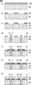
- 2 (a), FIG. 2 (b), FIG. 2 (c), FIG. 2 (d), FIG. 2 (e), FIG. 2 (f) and FIG. 2 (g) relate to one embodiment of the present invention.
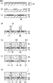
- 3 (a), 3 (b), 3 (c), 3 (d), 3 (e), 3 (f), and 3 (g) show another embodiment of the present invention.
- the present invention is not limited to the following configurations, and can be applied with appropriate modifications without departing from the scope of the present invention. It should be noted that the present invention also includes a combination of two or more desirable configurations of conductor connection structures according to one embodiment of the present invention described below.
- FIG. 1 is a cross-sectional view schematically showing an example of a conductor connection structure according to an embodiment of the present invention.
- FIG. 1 shows a substrate 30, a columnar conductor 10, a wiring pattern 20, and a plating electrode layer 50 that constitute the conductor connection structure 1.
- the conductor connection structure means a structure in which a columnar conductor, a wiring pattern, and a plating electrode layer are connected through a metal bond.
- An electronic component having a conductor connection structure means an electronic component in which such a conductor connection structure exists in any part of the electronic component.
- a conductive resin 40 that connects the columnar conductor 10 and the wiring pattern 20 is disposed between the columnar conductor 10 and the wiring pattern 20.
- the columnar conductor 10 passes through the substrate 30, and a part of the columnar conductor 10 protrudes from one main surface 31 of the substrate 30.
- the wiring pattern 20 is formed on one main surface 31 of the substrate 30.
- the upper surface 21 of the wiring pattern 20 is flat with respect to the upper surface 11 of the columnar conductor 10. In this specification, when the difference in height between the upper surface of the wiring pattern and the upper surface of the columnar conductor is 50% or less of the thickness of the wiring pattern, the upper surface of the wiring pattern is flat with respect to the upper surface of the columnar conductor.
- the difference in height between the upper surface of the wiring pattern and the upper surface of the columnar conductor can be measured by observing a cross-sectional photograph of a cross section cut at a portion including the upper surface of the wiring pattern and the upper surface of the columnar conductor.
- the thickness of the wiring pattern can also be measured by observing a cross-sectional photograph of a cross section cut at a portion including the upper and lower surfaces of the wiring pattern.
- the height measurement positions of the upper surface of the wiring pattern and the upper surface of the columnar conductor are the center of the upper surface of the wiring pattern and the center of the upper surface of the columnar conductor in the cross-sectional photograph.
- the thickness of the wiring pattern is measured by measuring the distance from the substrate at the center of the upper surface of the wiring pattern in the cross-sectional photograph. The height comparison between the upper surface of the wiring pattern and the upper surface of the columnar conductor is performed between the columnar conductor closest to the wiring pattern.
- the upper surface 41 of the conductive resin 40 disposed between the columnar conductor 10 and the wiring pattern 20 also preferably forms a flat surface together with the upper surface 21 of the wiring pattern 20 and the upper surface 11 of the columnar conductor 10.
- the conductive resin 40 is also formed on one main surface 31 of the substrate 30.
- the difference in height between the highest part and the lowest part of the surface formed by the upper surface of the conductive resin, the upper surface of the wiring pattern and the upper surface of the columnar conductor is 50% or less of the thickness of the wiring pattern
- the conductive resin And the surface formed by the upper surface of the wiring pattern, the upper surface of the wiring pattern, and the upper surface of the columnar conductor are defined to be flat.
- the height of the upper surface of the conductive resin can be measured by the above-described cross-sectional photograph, and the height of the conductive resin is measured at the center of the upper surface of the conductive resin in the cross-sectional photograph.
- the plating electrode layer 50 is provided on a flat surface formed by the upper surface 41 of the conductive resin 40, the upper surface 21 of the wiring pattern 20, and the upper surface 11 of the columnar conductor 10. For this reason, the plating electrode layer 50 is formed by plating growth from a flat surface, and has a uniform thickness and a smooth surface. In addition, since there is no step on the plating film formation surface, unplated (void) due to residual bubbles on the step is not formed, and a plating connection with high connection reliability can be stably formed.
- the plating electrode layer is formed by plating growth from the upper surface of the wiring pattern and the entire upper surface of the columnar conductor, it is connected to the upper surface of the wiring pattern by metal bonding, and is also connected to the entire upper surface of the columnar conductor by metal bonding. . Since the plating electrode layer is connected to the entire upper surface of the columnar conductor by metal bonding, the connection strength at the connection portion between the plating electrode layer and the columnar conductor is increased. Moreover, the electrical resistance in the connection part between a plating electrode layer and a columnar conductor becomes low, and the heat_generation
- the base substrate is preferably a resin substrate.
- a material usually used as a material for the resin substrate can be used.
- epoxy resin glass epoxy resin, phenol resin, fluororesin, silicone rubber, polyethylene, polypropylene, polystyrene, cycloolefin resin, liquid crystal polymer (LCP), polyimide resin, polyetheretherketone resin (PEEK), polyphenylene sulfide resin (PPS), polyetherimide resin, polyamideimide resin and the like.
- a ceramic substrate can also be used as the substrate.
- an LTCC substrate low temperature fired ceramic substrate
- an HTCC substrate high temperature fired ceramic substrate
- the thickness of the substrate is not particularly limited, but is preferably 0.5 mm or more and 10 mm or less.
- the substrate may be a multilayer substrate including a wiring pattern therein.
- a wiring pattern included in the multilayer substrate may be electrically connected to a wiring pattern formed on one main surface of the substrate through a via conductor or the like.
- a wiring pattern may also be formed on the other main surface of the substrate (the main surface opposite to the surface on which the plating electrode layer is provided).
- the columnar conductor is a conductor that penetrates the substrate and is a conductor that can electrically connect the upper and lower surfaces of the substrate.
- the upper surface of the columnar conductor protrudes from one main surface of the substrate.
- the height at which the columnar conductor protrudes from one main surface of the substrate is preferably equal to the thickness of the wiring pattern formed on the one main surface of the substrate.
- the height at which the columnar conductor protrudes from one main surface of the substrate is preferably 5 ⁇ m or more and 400 ⁇ m or less.
- the length of the columnar conductor is preferably 0.5 mm or more and 10 mm or less.
- the columnar conductor is preferably a metal pin, and the shape thereof is preferably prismatic, cylindrical or elliptical.
- the area of the upper surface of the columnar conductor is 0.005 mm 2 or more and 3.5 mm 2 or less. When the area of the upper surface of the columnar conductor is 0.005 mm 2 or more, the connection strength is large because the area connected to the plating electrode layer through the metal bond is sufficiently large, and the electrical resistance at the connection portion is small. Therefore, it is preferable.
- the material of the columnar conductor is preferably Cu or an alloy containing Cu. CuNi alloy etc. are mentioned as an alloy containing Cu.
- the wiring pattern is a wiring pattern formed on one main surface of the substrate, and may be a line-shaped wiring or a so-called solid electrode having a large area.
- the wiring pattern formed on one main surface of the substrate may be electrically connected to the wiring inside the substrate.
- a via conductor or a through-hole conductor for drawing out the wiring inside the substrate to the one main surface side of the substrate is provided on the substrate and connected to the wiring pattern formed on the one main surface of the substrate.
- the wiring pattern is preferably made of a metal foil, and a copper foil can be preferably used as the metal foil. By using the metal foil as the wiring pattern, for example, wiring defects such as disconnection inside the wiring are less likely to occur than when the wiring pattern is made of a conductive paste.
- the thickness of the wiring pattern is preferably 5 ⁇ m or more and 400 ⁇ m or less.
- the thickness of the metal foil is the thickness of the wiring pattern.
- it can be set as the board
- the plating electrode layer is provided on the entire upper surface of the columnar conductor and the upper surface of the wiring pattern, and is connected to the columnar conductor via a metal bond, and is also connected to the wiring pattern via a metal bond. . As a result, the columnar conductor and the wiring pattern are also connected through a metal bond.
- the plating electrode layer is preferably any one of an electroless plating film, an electrolytic plating film, or a combination of an electroless plating film and an electrolytic plating film. Since both the upper surface of the columnar conductor and the upper surface of the wiring pattern can be plated, it is suitable for forming a plating electrode layer.
- the material of the plating electrode layer is preferably copper, and in addition to copper, a metal such as nickel or tin, or an alloy containing at least one metal selected from the group consisting of copper, nickel and tin is used. Can do. Further, a plating film made of another metal such as nickel plating or gold plating may be further provided on the plating electrode layer.
- the thickness of the plating electrode layer is preferably 5 ⁇ m or more and 400 ⁇ m or less. Further, the plating electrode layer can be a layer having a uniform thickness, and the thickness variation (difference between the maximum thickness and the minimum thickness of the plating electrode layer) is preferably a layer of ⁇ 20% or less.
- the conductive resin is preferably disposed between the columnar conductor and the wiring pattern on one main surface of the substrate.
- the conductive resin fills the space between the columnar conductor and the wiring pattern, and can physically connect the columnar conductor and the wiring pattern.
- the conductive resin can be flattened between the upper surface of the columnar conductor and the upper surface of the wiring pattern, and the conductive resin can be a film-forming surface for plating growth. It can be made more uniform.
- a conductive resin in which a resin and a conductive material are mixed can be used.
- As the conductive material Au, Ag, Cu, or an alloy containing these metals can be used.
- resin the resin quoted as resin which can be used for a resin substrate can be used.
- the thickness of the conductive resin is preferably a thickness capable of forming a flat surface with the upper surface of the columnar conductor and the upper surface of the wiring pattern, and is preferably the same as or approximately the same as the thickness of the wiring pattern. Moreover, it is preferable that it is the same as the height which the columnar conductor protrudes from one main surface of a board
- the conductor connection structure described so far is suitable as a structure included in an electronic component.
- Examples of electronic components suitable for providing such a conductor connection structure include a coil, an antenna, and a power supply module.
- FIG. 2 (a), FIG. 2 (b), FIG. 2 (c), FIG. 2 (d), FIG. 2 (e), FIG. 2 (f) and FIG. 2 (g) relate to one embodiment of the present invention. It is process drawing which shows typically the manufacturing method of the connection structure of a conductor.
- a substrate 30 having a base electrode layer 120 formed on one main surface thereof is prepared.
- a metal foil is preferably used as the base electrode layer, and a copper foil can be preferably used as the metal foil.
- a part of the base electrode layer 120 is removed to form a wiring pattern 20.
- the method for removing the base electrode layer may be a physical method (grinding or physical etching) or a chemical method (chemical etching).
- a through hole 60 is formed in a portion of the substrate 30 where the base electrode layer is partially removed. Formation of the through hole can be performed by a drilling technique such as a laser or a drill. Then, the columnar conductor 10 is formed in the through hole 60 as shown in FIG.
- the columnar conductor can be formed by a method of inserting a metal pin into the through hole or filling a hole by plating. In particular, a columnar conductor can be easily formed by using a metal pin.
- the length of the columnar conductor 10 is preferably determined so that the upper surface 11 of the columnar conductor 10 is aligned with the upper surface 21 of the wiring pattern 20, but may not be completely aligned because a planarization process is performed later.
- FIG. 2D shows an example in which the upper surface 11 of the columnar conductor 10 protrudes from the upper surface 21 of the wiring pattern 20.
- the space between the columnar conductor 10 and the wiring pattern 20 is filled with a conductive resin 40.
- a conductive resin having fluidity in a space between the columnar conductor and the wiring pattern and curing the resin By flowing a conductive resin having fluidity in a space between the columnar conductor and the wiring pattern and curing the resin, the columnar conductor and the wiring pattern can be physically connected by the conductive resin.
- the height of the upper surface 41 of the conductive resin 40 is preferably determined so as to be aligned with the upper surface 21 of the wiring pattern 20 and the upper surface 11 of the columnar conductor 10, but may not be completely aligned because a planarization process is performed later.
- FIG. 2E shows an example where the upper surface 41 of the conductive resin 40 protrudes from the upper surface 21 of the wiring pattern 20. It is not essential to fill the space between the columnar conductor and the wiring pattern with a conductive resin.
- a flattening process is performed in which the protruding portions of the upper surface 11 of the columnar conductor 10, the upper surface 21 of the wiring pattern 20, and the upper surface 41 of the conductive resin 40 are cut and flattened.
- the flattening step can be performed by a method such as mechanical polishing such as lapping or polishing.
- a flat surface is obtained in which the upper surface 11 of the columnar conductor 10, the upper surface 21 of the wiring pattern 20, and the upper surface 41 of the conductive resin 40 are flat.
- the difference in height between the highest and lowest portions of the surface formed by the upper surface of the conductive resin, the upper surface of the wiring pattern, and the upper surface of the columnar conductor is 50% or less of the thickness of the wiring pattern.
- flattening is performed so that the difference in height between the upper surface of the wiring pattern and the upper surface of the columnar conductor is 50% or less of the thickness of the wiring pattern.
- a plating electrode layer 50 is formed on the upper surface 11 of the planarized columnar conductor 10, the upper surface 21 of the wiring pattern 20, and the upper surface 41 of the conductive resin 40.
- the plating electrode layer is preferably formed by electroless plating, electrolytic plating, or a combination of electroless plating and electrolytic plating.
- the flat surface obtained before the formation of the plating electrode layer is a surface formed of a conductive material, and serves as a film-forming surface for plating growth, so that both electroless plating and electrolytic plating methods can be applied. can do.
- the conductor connection structure 1 is obtained by the above process.
- 3 (a), 3 (b), 3 (c), 3 (d), 3 (e), 3 (f), and 3 (g) show another embodiment of the present invention. It is process drawing which shows typically the manufacturing method of the connection structure of the said conductor.
- a base 170 with an electrode layer in which a base electrode layer 120 is provided on a base 70 is prepared.
- the pedestal is a plate-like material whose main surface is a flat surface.
- the main surface of the pedestal is a surface on which a base electrode layer is provided to form a wiring pattern, and the difference in height between the highest portion and the lowest portion on the main surface of the pedestal is the thickness of the wiring pattern to be formed later. %, And such a pedestal is a pedestal whose main surface is a flat surface.
- a metal foil is preferably used as the base electrode layer, and a copper foil can be preferably used as the metal foil.
- a method of bonding a metal foil to the pedestal with an adhesive can be used.
- bonding if an adhesive capable of performing cold peeling, foaming peeling, UV peeling or the like is used later, it is easy to remove the pedestal in a later process.
- the “substrate” portion of the substrate with metal foil is flat, the “substrate” portion is regarded as a pedestal, and the substrate with metal foil in which metal foil is provided in advance on one main surface of the substrate is used as a base electrode layer. You may prepare as a base with an electrode layer provided with.
- the substrate portion (portion corresponding to the base) of the substrate with metal foil is removed later, the “substrate” in the obtained conductor connection structure is different from the “substrate” of the substrate with metal foil.
- a part of the base electrode layer 120 is removed to form a wiring pattern 20.
- the method for removing the base electrode layer may be a physical method (grinding or physical etching) or a chemical method (chemical etching).
- the portion from which the base electrode layer has been removed is filled with a conductive resin 40.
- the conductive resin at this time is in a state before being cured.
- the columnar conductor 10 is inserted into the conductive resin 40 until the bottom surface 111 of the columnar conductor 10 contacts the pedestal 70, and the conductive resin 40 is further cured to form the columnar conductor on the pedestal 70. 10 is fixed.
- the resin layer 30 is formed on the surface 122 of the wiring pattern 20 and the surface 142 of the conductive resin 40.
- the resin layer can be formed by injecting a fluid resin material or a liquid containing the resin material and curing the resin material.
- the resin layer 30 becomes the substrate 30 in the manufactured conductor connection structure 1.
- the resin layer is preferably formed to the same height as the columnar conductor. Further, after forming the resin layer so as to cover the columnar conductor, the resin layer may be polished so that the columnar conductor is exposed from the resin layer.
- the pedestal 70 is removed as shown in FIG.
- the removal of the pedestal 70 can be performed by mechanical polishing. Further, when an adhesive capable of performing cold peeling, foaming peeling, or UV peeling is used when providing the base electrode layer on the pedestal, the pedestal may be peeled off using these peeling methods. .
- the pedestal By removing the pedestal, the bottom surface 111 of the columnar conductor 10, the back surface 121 of the wiring pattern 20, and the back surface 141 of the conductive resin 40 are exposed.
- the bottom surface 111 of the columnar conductor 10, the back surface 121 of the wiring pattern 20, and the back surface 141 of the conductive resin 40 are all in contact with the pedestal 70, and the pedestal 70 is a material whose main surface is flat.
- the back surface 121 and the back surface 141 of the conductive resin 40 are flat surfaces.
- the bottom surface 111 of the columnar conductor 10, the back surface 121 of the wiring pattern 20, and the back surface 141 of the conductive resin 40 are respectively the top surface of the columnar conductor, the top surface of the wiring pattern, and the top surface of the conductive resin in the conductor connection structure of the present invention. Since it is not necessary to perform a further flattening step on the flat surface obtained in this way, the whole can be simplified.
- the plating electrode layer 50 is formed on the bottom surface 111 of the columnar conductor 10, the back surface 121 of the wiring pattern 20, and the back surface 141 of the conductive resin 40.
- the plating electrode layer is preferably formed by electroless plating, electrolytic plating, or a combination of electroless plating and electrolytic plating. It is preferable that a conductive resin is provided between the columnar conductor and the wiring pattern because a depression between the columnar conductor and the wiring pattern is prevented when forming the plating electrode layer.
- the conductor connection structure 1 is obtained by the above process.
- the conductor connection structure 1 shown in FIG. 3G is the same as the conductor connection structure 1 shown in FIG. 1 and FIG.
- the present invention can be applied to any part of the electronic component by using the conductor connection structure manufacturing method described above in any step of the electronic component manufacturing process.
- a conductor connection structure may be formed.
Landscapes
- Engineering & Computer Science (AREA)
- Manufacturing & Machinery (AREA)
- Microelectronics & Electronic Packaging (AREA)
- Printing Elements For Providing Electric Connections Between Printed Circuits (AREA)
Abstract
本発明の導体の接続構造は、ベースとなる基板と、上記基板を貫通する柱状導体と、少なくとも上記基板の一主面に形成され、その上面が上記柱状導体の上面に対して平坦である配線パターンと、上記柱状導体の上面全体と上記配線パターンの上面の上に設けられ、上記柱状導体と上記配線パターンとを金属結合を介して接続するめっき電極層と、を備えることを特徴とする。
Description
本発明は、導体の接続構造、電子部品、導体の接続構造の製造方法及び電子部品の製造方法に関する。
各種電子機器に用いられる回路基板として、金属ピンを柱状導体として使用した基板が知られている。
特許文献1には、絶縁層に形成された配線電極パターンと、該配線電極パターンに接続された柱状導体とを備える電子装置が開示されている。
特許文献1に開示された電子装置では、配線電極パターンが、導電性ペーストにより形成された下地電極層と、該下地電極層に積層されためっき電極層とにより形成されている。
下地電極層は、柱状導体の端面の一部を被覆するように形成されており、柱状導体の端面の下地電極層に被覆されていない部分がめっき電極層により被覆されている。
特許文献1に開示された電子装置では、配線電極パターンが、導電性ペーストにより形成された下地電極層と、該下地電極層に積層されためっき電極層とにより形成されている。
下地電極層は、柱状導体の端面の一部を被覆するように形成されており、柱状導体の端面の下地電極層に被覆されていない部分がめっき電極層により被覆されている。
特許文献1に記載された電子装置では、柱状導体と配線電極パターンの接続が、導電性ペーストにより形成された下地電極層とめっき電極層からなるが、導電性ペーストにより形成された下地電極層は柱状導体との接続強度が弱いため、柱状導体と配線電極パターンの接続が全体として弱くなるという問題があった。
また、柱状導体と配線電極パターンの接続が、導電性ペーストにより形成された下地電極層とめっき電極層の2種類の電極層との間でされているが、抵抗の低いめっき電極層により接続された部分が狭くなるため、柱状導体と配線電極パターンの接続部分における電気抵抗が高くなり、発熱箇所となる可能性があった。
また、配線電極パターンが、導電性ペーストにより形成された下地電極層とめっき電極層の2種類からなるため、配線電極パターン表面において下地電極層が存在する部分と存在しない部分で段差を生じており、段差により配線電極パターンと柱状導体の接続が不安定になることがあった。
さらに、導電性ペーストにより形成された下地電極層は配線内部での膨れ、断線などの不具合を生じる可能性があった。
また、柱状導体と配線電極パターンの接続が、導電性ペーストにより形成された下地電極層とめっき電極層の2種類の電極層との間でされているが、抵抗の低いめっき電極層により接続された部分が狭くなるため、柱状導体と配線電極パターンの接続部分における電気抵抗が高くなり、発熱箇所となる可能性があった。
また、配線電極パターンが、導電性ペーストにより形成された下地電極層とめっき電極層の2種類からなるため、配線電極パターン表面において下地電極層が存在する部分と存在しない部分で段差を生じており、段差により配線電極パターンと柱状導体の接続が不安定になることがあった。
さらに、導電性ペーストにより形成された下地電極層は配線内部での膨れ、断線などの不具合を生じる可能性があった。
このように、柱状導体と配線電極パターンの接続が、導電性ペーストにより形成された下地電極層とめっき電極層の2種類の電極層によってなされる構造では、いくつかの問題が生じることがあった。
本発明は上記の問題を解決するためになされたものであり、柱状導体と配線パターンとの接続が良好に達成された導体の接続構造を提供することを目的とする。
本発明は上記の問題を解決するためになされたものであり、柱状導体と配線パターンとの接続が良好に達成された導体の接続構造を提供することを目的とする。
本発明の一態様に係る導体の接続構造は、ベースとなる基板と、上記基板を貫通する柱状導体と、少なくとも上記基板の一主面に形成され、その上面が上記柱状導体の上面に対して平坦である配線パターンと、上記柱状導体の上面全体と上記配線パターンの上面の上に設けられ、上記柱状導体と上記配線パターンとを金属結合を介して接続するめっき電極層と、を備えることを特徴とする。
本発明の一態様に係る導体の接続構造では、柱状導体の上面全体と配線パターンの上面がともにめっき電極層と金属結合を介して接続されている。
本明細書における金属結合とは、金属同士が接着剤を介さずに結合していることを意味している。
柱状導体の上面全体が金属結合を介してめっき電極層と接続されるため、柱状導体の上面の一部を導電性ペーストで接続するよりも、接続部分における電気抵抗が低くなる。そのため接続部分での発熱が少なくなる。
また、柱状導体の上面全体が金属結合を介してめっき電極層と接続されているため、柱状導体の上面の一部を導電性ペーストで接続するよりも、接続部分における接続強度が強くなる。
また、配線パターンの上面が柱状導体の上面と平坦な面となっていると、配線パターンの上面と柱状導体の上面の同じ高さからのめっき成長によりめっき電極層を形成することができる。そのため、膜厚が均一なめっき電極層を形成することができる。
また、めっき成膜面である柱状導体の上面と配線パターンの上面に段差が無いため、段差への気泡残留による未めっき(ボイド)が形成されず、接続信頼性の高いめっき接続を安定して形成することができる。
本明細書における金属結合とは、金属同士が接着剤を介さずに結合していることを意味している。
柱状導体の上面全体が金属結合を介してめっき電極層と接続されるため、柱状導体の上面の一部を導電性ペーストで接続するよりも、接続部分における電気抵抗が低くなる。そのため接続部分での発熱が少なくなる。
また、柱状導体の上面全体が金属結合を介してめっき電極層と接続されているため、柱状導体の上面の一部を導電性ペーストで接続するよりも、接続部分における接続強度が強くなる。
また、配線パターンの上面が柱状導体の上面と平坦な面となっていると、配線パターンの上面と柱状導体の上面の同じ高さからのめっき成長によりめっき電極層を形成することができる。そのため、膜厚が均一なめっき電極層を形成することができる。
また、めっき成膜面である柱状導体の上面と配線パターンの上面に段差が無いため、段差への気泡残留による未めっき(ボイド)が形成されず、接続信頼性の高いめっき接続を安定して形成することができる。
本発明の一態様に係る導体の接続構造では、上記柱状導体と上記配線パターンの間に、上記柱状導体と上記配線パターンを接続する導電樹脂が配置されていることが好ましい。
導電樹脂は、柱状導体と配線パターンの間を埋めて、柱状導体と配線パターンを物理的に接続することができる。
また、導電樹脂を配置することで柱状導体の上面と配線パターンの上面の間が平坦になり、導電樹脂はめっき成長のための成膜面となることができるので、めっき電極層の膜厚をより均一にすることができる。
導電樹脂は、柱状導体と配線パターンの間を埋めて、柱状導体と配線パターンを物理的に接続することができる。
また、導電樹脂を配置することで柱状導体の上面と配線パターンの上面の間が平坦になり、導電樹脂はめっき成長のための成膜面となることができるので、めっき電極層の膜厚をより均一にすることができる。
本発明の一態様に係る導体の接続構造では、上記配線パターンは金属箔からなることが好ましい。
配線パターンを金属箔とすることで、配線パターンが導電性ペーストからなる場合に比べて、配線内部での断線等の配線不良が起こりにくくなる。
配線パターンを金属箔とすることで、配線パターンが導電性ペーストからなる場合に比べて、配線内部での断線等の配線不良が起こりにくくなる。
本発明の一態様に係る導体の接続構造では、上記柱状導体は金属ピンであることが好ましい。
金属ピンの上面はめっき成長の成膜面として適しており、金属ピンの上面とめっき電極層の間には金属結合による強固な接続が達成される。
金属ピンの上面はめっき成長の成膜面として適しており、金属ピンの上面とめっき電極層の間には金属結合による強固な接続が達成される。
本発明の一態様に係る導体の接続構造では、上記基板が樹脂基板であることが好ましい。
樹脂基板は孔開け加工、サイズ加工等の加工が容易であり、設計自由度が高い。
樹脂基板は孔開け加工、サイズ加工等の加工が容易であり、設計自由度が高い。
本発明の一態様に係る電子部品は、本発明の一態様に係る導体の接続構造を備えることを特徴とする。
本発明の導体の接続構造を備えた電子部品は、柱状導体と配線パターンの接続信頼性が高く、柱状導体と配線パターンの接続部分における発熱の少ない電子部品とすることができる。
本発明の導体の接続構造を備えた電子部品は、柱状導体と配線パターンの接続信頼性が高く、柱状導体と配線パターンの接続部分における発熱の少ない電子部品とすることができる。
本発明の一態様に係る導体の接続構造の製造方法は、下地電極層が形成された基板を用意する工程と、上記下地電極層の一部を除去し、配線パターンを形成する工程と、上記基板の上記下地電極層が一部除去された部分に貫通孔を形成する工程と、上記貫通孔に柱状導体を形成する工程と、上記柱状導体の上面及び上記配線パターンの上面の突出した部分を削って平坦化し、上記柱状導体の上面に対して上記配線パターンの上面を平坦にする平坦化工程と、上記柱状導体の上面全体及び上記配線パターンの上面にめっき電極層を形成する工程とを有することを特徴とする。
上記工程であると、めっき電極層を形成する前の柱状導体の上面に対して配線パターンの上面が平坦になっている。このような柱状導体の上面全体及び配線パターンの上面からめっき成長によりめっき電極層を形成することにより、段差のない平滑なめっき電極層が得られる。また、めっき電極層の膜厚の制御も容易になり、めっき電極層の膜厚のばらつきも小さくすることができる。
また、表皮効果による表皮抵抗の減少効果を得るためには段差のないめっき電極層が好ましいが、段差のないめっき電極層を得るために研磨でめっき電極層表面を処理すると表面粗さが粗くなり信号の移動距離が長くなるため損失が大きくなってしまう。
上記工程では、段差がない平滑なめっき電極層が得られるためこのような問題が生じず、損失の小さな導体の接続構造を得ることができる。
また、表皮効果による表皮抵抗の減少効果を得るためには段差のないめっき電極層が好ましいが、段差のないめっき電極層を得るために研磨でめっき電極層表面を処理すると表面粗さが粗くなり信号の移動距離が長くなるため損失が大きくなってしまう。
上記工程では、段差がない平滑なめっき電極層が得られるためこのような問題が生じず、損失の小さな導体の接続構造を得ることができる。
また、本発明の一態様に係る導体の接続構造の製造方法は、柱状導体を形成する工程の後に、上記柱状導体と上記配線パターンの間を導電樹脂で埋める工程を有し、上記平坦化工程において、上記導電樹脂の上面の突出した部分も削って平坦化し、上記めっき電極層を形成する工程において、上記導電樹脂の上面にもめっき電極層を形成することが好ましい。
導電樹脂は、柱状導体と配線パターンの間を埋めて、柱状導体と配線パターンを物理的に接続することができる。
また、平坦化工程において導電樹脂も削って平坦化することで柱状導体の上面と配線パターンの上面の間が平坦になり、導電樹脂はめっき成長のための成膜面となることができるので、めっき電極層の膜厚をより均一にすることができる。
導電樹脂は、柱状導体と配線パターンの間を埋めて、柱状導体と配線パターンを物理的に接続することができる。
また、平坦化工程において導電樹脂も削って平坦化することで柱状導体の上面と配線パターンの上面の間が平坦になり、導電樹脂はめっき成長のための成膜面となることができるので、めっき電極層の膜厚をより均一にすることができる。
本発明の別の態様に係る導体の接続構造の製造方法は、その主面が平坦面である台座の主面に下地電極層が設けられた電極層付き台座を用意する工程と、上記下地電極層の一部を除去し、配線パターンを形成する工程と、上記下地電極層が除去された部分を導電樹脂で埋める工程と、上記導電樹脂に柱状導体を柱状導体の底面が上記台座と接触するまで挿入し、上記導電樹脂を硬化させて台座上に上記柱状導体を固定する工程と、上記配線パターンの表面及び上記導電樹脂の表面に樹脂層を形成する工程と、上記台座を除去し、上記柱状導体の底面、上記配線パターンの裏面及び上記導電樹脂の裏面が平坦である平坦面を露出させる工程と、上記柱状導体の底面、上記配線パターンの裏面及び上記導電樹脂の裏面にめっき電極層を形成する工程とを有することを特徴とする。
上記工程では、台座を除去した段階で柱状導体の底面、配線パターンの裏面及び導電樹脂の裏面が平坦である平坦面となる。この平坦面はめっき電極層を形成することのできる面であり、この平坦面にめっき電極層を形成することにより、段差のない平滑なめっき電極層が得られる。また、めっき電極層の膜厚の制御も容易になり、めっき電極層の膜厚のばらつきも小さくすることができる。
この工程では平坦面を得るための平坦化加工の工程を必要としない点で簡潔な工程とすることができる。
また、段差がない平滑なめっき電極層が得られるため、損失の小さな導体の接続構造を得ることができる。
この工程では平坦面を得るための平坦化加工の工程を必要としない点で簡潔な工程とすることができる。
また、段差がない平滑なめっき電極層が得られるため、損失の小さな導体の接続構造を得ることができる。
本発明の各態様に係る導体の接続構造の製造方法では、めっき電極層の形成を、無電解めっき、電解めっき又は無電解めっきと電解めっきの併用で行うことが好ましい。
めっき電極層の形成前に得られる平坦面は、導電性を有する材料により形成された面であり、めっき成長のための成膜面となるので無電解めっき、電解めっきのいずれのめっき方法も適用することができる。
めっき電極層の形成前に得られる平坦面は、導電性を有する材料により形成された面であり、めっき成長のための成膜面となるので無電解めっき、電解めっきのいずれのめっき方法も適用することができる。
本発明の一態様に係る電子部品の製造方法は、本発明のいずれかの態様に係る製造方法により導体の接続構造を製造する工程を含むことを特徴とする。
この製造方法によると、柱状導体と配線パターンの接続信頼性が高く、柱状導体と配線パターンの接続部分における発熱の少ない電子部品を製造することができる。
この製造方法によると、柱状導体と配線パターンの接続信頼性が高く、柱状導体と配線パターンの接続部分における発熱の少ない電子部品を製造することができる。
本発明によれば、柱状導体と配線パターンとの接続が良好に達成された導体の接続構造を得ることができる。
以下、本発明の一実施の形態に係る導体の接続構造について説明する。
しかしながら、本発明は、以下の構成に限定されるものではなく、本発明の要旨を変更しない範囲において適宜変更して適用することができる。なお、以下において記載する本発明の一実施の形態に係る導体の接続構造の個々の望ましい構成を2つ以上組み合わせたものもまた本発明である。
しかしながら、本発明は、以下の構成に限定されるものではなく、本発明の要旨を変更しない範囲において適宜変更して適用することができる。なお、以下において記載する本発明の一実施の形態に係る導体の接続構造の個々の望ましい構成を2つ以上組み合わせたものもまた本発明である。
図1は、本発明の一実施の形態に係る導体の接続構造の一例を模式的に示す断面図である。
図1には、導体の接続構造1を構成する基板30、柱状導体10、配線パターン20、めっき電極層50を示している。導体の接続構造とは、柱状導体と配線パターンとめっき電極層が金属結合を介して接続された構造を意味している。
また、導体の接続構造を備える電子部品とは、このような導体の接続構造が電子部品のいずれかの部位に存在する電子部品を意味している。
図1に示す導体の接続構造1においては、柱状導体10と配線パターン20の間に、柱状導体10と配線パターン20を接続する導電樹脂40が配置されている。
図1には、導体の接続構造1を構成する基板30、柱状導体10、配線パターン20、めっき電極層50を示している。導体の接続構造とは、柱状導体と配線パターンとめっき電極層が金属結合を介して接続された構造を意味している。
また、導体の接続構造を備える電子部品とは、このような導体の接続構造が電子部品のいずれかの部位に存在する電子部品を意味している。
図1に示す導体の接続構造1においては、柱状導体10と配線パターン20の間に、柱状導体10と配線パターン20を接続する導電樹脂40が配置されている。
柱状導体10は基板30を貫通しており、柱状導体10の一部は基板30の一主面31から突出している。また、配線パターン20は基板30の一主面31に形成されている。
そして、配線パターン20の上面21は、柱状導体10の上面11に対して平坦となっている。
本明細書では、配線パターンの上面と柱状導体の上面の高さの差が、配線パターンの厚さの50%以下である場合に、配線パターンの上面が柱状導体の上面に対して平坦となっていると定める。
配線パターンの上面と柱状導体の上面の高さの差の測定は、配線パターンの上面と柱状導体の上面を含む部位で切断した断面の断面写真を観察することにより行うことができる。また、配線パターンの厚さの測定も配線パターンの上下面を含む部位で切断した断面の断面写真を観察することにより行うことができる。
配線パターンの上面と柱状導体の上面の高さの測定位置は、断面写真における配線パターンの上面の中央及び柱状導体の上面の中央とする。
また、配線パターンの厚さの測定は断面写真における配線パターンの上面の中央における基板からの距離を測定することで行うこととする。
配線パターンの上面と柱状導体の上面の高さの比較は、配線パターンに対して最も近い柱状導体との間で行う。
そして、配線パターン20の上面21は、柱状導体10の上面11に対して平坦となっている。
本明細書では、配線パターンの上面と柱状導体の上面の高さの差が、配線パターンの厚さの50%以下である場合に、配線パターンの上面が柱状導体の上面に対して平坦となっていると定める。
配線パターンの上面と柱状導体の上面の高さの差の測定は、配線パターンの上面と柱状導体の上面を含む部位で切断した断面の断面写真を観察することにより行うことができる。また、配線パターンの厚さの測定も配線パターンの上下面を含む部位で切断した断面の断面写真を観察することにより行うことができる。
配線パターンの上面と柱状導体の上面の高さの測定位置は、断面写真における配線パターンの上面の中央及び柱状導体の上面の中央とする。
また、配線パターンの厚さの測定は断面写真における配線パターンの上面の中央における基板からの距離を測定することで行うこととする。
配線パターンの上面と柱状導体の上面の高さの比較は、配線パターンに対して最も近い柱状導体との間で行う。
また、柱状導体10と配線パターン20の間に配置された導電樹脂40の上面41も、配線パターン20の上面21と柱状導体10の上面11とともに平坦な面を形成していることが好ましい。導電樹脂40も基板30の一主面31上に形成されている。
導電樹脂の上面、配線パターンの上面及び柱状導体の上面で形成される面の最も高い箇所と最も低い箇所の高さの差が、配線パターンの厚さの50%以下である場合に、導電樹脂の上面、配線パターンの上面及び柱状導体の上面で形成される面が平坦となっていると定める。
導電樹脂の上面の高さの測定は、上述した断面写真により行うことができ、導電樹脂の高さの測定位置は断面写真における導電樹脂の上面の中央とする。
導電樹脂の上面、配線パターンの上面及び柱状導体の上面で形成される面の最も高い箇所と最も低い箇所の高さの差が、配線パターンの厚さの50%以下である場合に、導電樹脂の上面、配線パターンの上面及び柱状導体の上面で形成される面が平坦となっていると定める。
導電樹脂の上面の高さの測定は、上述した断面写真により行うことができ、導電樹脂の高さの測定位置は断面写真における導電樹脂の上面の中央とする。
めっき電極層50は、導電樹脂40の上面41、配線パターン20の上面21及び柱状導体10の上面11で形成される平坦な面の上に設けられている。そのため、めっき電極層50は平坦な面からめっき成長して形成された、膜厚が均一かつ表面が平滑な面となる。
また、めっき成膜面に段差が無いため、段差への気泡残留による未めっき(ボイド)が形成されず、接続信頼性の高いめっき接続を安定して形成することができる。
また、めっき成膜面に段差が無いため、段差への気泡残留による未めっき(ボイド)が形成されず、接続信頼性の高いめっき接続を安定して形成することができる。
めっき電極層は配線パターンの上面及び柱状導体の上面全体からめっき成長して形成されるので、配線パターンの上面と金属結合によって接続されており、柱状導体の上面全体とも金属結合によって接続されている。
めっき電極層は柱状導体の上面全体と金属結合により接続されるので、めっき電極層と柱状導体の間の接続部分における接続強度が強くなる。また、めっき電極層と柱状導体の間の接続部分における電気抵抗が低くなり、接続部分での発熱が少なくなる。
めっき電極層は柱状導体の上面全体と金属結合により接続されるので、めっき電極層と柱状導体の間の接続部分における接続強度が強くなる。また、めっき電極層と柱状導体の間の接続部分における電気抵抗が低くなり、接続部分での発熱が少なくなる。
以下、導体の接続構造の各構成要素について説明する。
ベースとなる基板は、樹脂基板であることが好ましい。
樹脂としては樹脂基板の材料として通常使用される材料を使用することができる。
例えば、エポキシ樹脂、ガラスエポキシ樹脂、フェノール樹脂、フッ素樹脂、シリコーンゴム、ポリエチレン、ポリプロピレン、ポリスチレン、シクロオレフィン系樹脂、液晶ポリマー(LCP)、ポリイミド樹脂、ポリエーテルエーテルケトン樹脂(PEEK)、ポリフェニレンスルフィド樹脂(PPS)、ポリエーテルイミド樹脂、ポリアミドイミド樹脂等が挙げられる。
また、基板としてセラミック基板を使用することもできる。セラミック基板としてはLTCC基板(低温焼成セラミック基板)、HTCC基板(高温焼成セラミック基板)等を使用することができる。
基板の厚さは特に限定されるものではないが、0.5mm以上、10mm以下であることが好ましい。
基板は、その内部に配線パターンを含む多層基板であってもよい。多層基板内に含まれる配線パターンが、ビア導体等を介して基板の一主面に形成された配線パターンと電気的に接続されていてもよい。
また、基板の他方主面(めっき電極層が設けられる面と反対側の主面)にも配線パターンが形成されていてもよい。
ベースとなる基板は、樹脂基板であることが好ましい。
樹脂としては樹脂基板の材料として通常使用される材料を使用することができる。
例えば、エポキシ樹脂、ガラスエポキシ樹脂、フェノール樹脂、フッ素樹脂、シリコーンゴム、ポリエチレン、ポリプロピレン、ポリスチレン、シクロオレフィン系樹脂、液晶ポリマー(LCP)、ポリイミド樹脂、ポリエーテルエーテルケトン樹脂(PEEK)、ポリフェニレンスルフィド樹脂(PPS)、ポリエーテルイミド樹脂、ポリアミドイミド樹脂等が挙げられる。
また、基板としてセラミック基板を使用することもできる。セラミック基板としてはLTCC基板(低温焼成セラミック基板)、HTCC基板(高温焼成セラミック基板)等を使用することができる。
基板の厚さは特に限定されるものではないが、0.5mm以上、10mm以下であることが好ましい。
基板は、その内部に配線パターンを含む多層基板であってもよい。多層基板内に含まれる配線パターンが、ビア導体等を介して基板の一主面に形成された配線パターンと電気的に接続されていてもよい。
また、基板の他方主面(めっき電極層が設けられる面と反対側の主面)にも配線パターンが形成されていてもよい。
柱状導体は、基板を貫通する導体であり、基板の上下面を電気的に接続することができる導体である。
配線パターンの上面と平坦面を形成するために、柱状導体の上面は基板の一主面から突出している。柱状導体が基板の一主面から突出する高さは、基板の一主面に形成される配線パターンの厚さと等しいことが好ましい。
例えば、柱状導体が基板の一主面から突出する高さが5μm以上、400μm以下であることが好ましい。
また、柱状導体の長さは0.5mm以上、10mm以下であることが好ましい。
柱状導体は金属ピンであることが好ましく、その形状は角柱状、円柱状又は楕円柱状であることが好ましい。また、柱状導体の上面の面積が0.005mm2以上、3.5mm2以下であることが好ましい。柱状導体の上面の面積が0.005mm2以上であると、めっき電極層と金属結合を介して接続される面積が充分に大きいために接続強度が大きく、また、接続部分での電気抵抗が小さくなるため好ましい。
また、柱状導体の材質は、Cu又はCuを含む合金であることが好ましい。Cuを含む合金としてはCuNi合金等が挙げられる。
配線パターンの上面と平坦面を形成するために、柱状導体の上面は基板の一主面から突出している。柱状導体が基板の一主面から突出する高さは、基板の一主面に形成される配線パターンの厚さと等しいことが好ましい。
例えば、柱状導体が基板の一主面から突出する高さが5μm以上、400μm以下であることが好ましい。
また、柱状導体の長さは0.5mm以上、10mm以下であることが好ましい。
柱状導体は金属ピンであることが好ましく、その形状は角柱状、円柱状又は楕円柱状であることが好ましい。また、柱状導体の上面の面積が0.005mm2以上、3.5mm2以下であることが好ましい。柱状導体の上面の面積が0.005mm2以上であると、めっき電極層と金属結合を介して接続される面積が充分に大きいために接続強度が大きく、また、接続部分での電気抵抗が小さくなるため好ましい。
また、柱状導体の材質は、Cu又はCuを含む合金であることが好ましい。Cuを含む合金としてはCuNi合金等が挙げられる。
配線パターンは、基板の一主面に形成された配線パターンであり、ライン状の配線であってもよく、大面積を有するいわゆるベタ電極であってもよい。
また、基板の一主面に形成された配線パターンは基板内部の配線と電気的に接続されていてもよい。その場合、基板内部の配線を基板の一主面側に引き出すためのビア導体やスルーホール導体が基板に設けられ、基板の一主面に形成された配線パターンと接続されることが好ましい。
配線パターンは金属箔からなることが好ましく、金属箔として好ましくは銅箔を使用することができる。配線パターンを金属箔とすることで、例えば配線パターンを導電性ペーストとする場合に比べて、配線内部での断線等の配線不良が起こりにくくなる。
配線パターンの厚さは5μm以上、400μm以下であることが好ましい。
配線パターンが金属箔からなる場合、金属箔の厚さが配線パターンの厚さとなる。
また、基板の一主面に金属箔があらかじめ設けられた金属箔付き基板を出発材料とすることにより、金属箔からなる配線パターンを有する基板とすることができる。
また、基板の一主面に形成された配線パターンは基板内部の配線と電気的に接続されていてもよい。その場合、基板内部の配線を基板の一主面側に引き出すためのビア導体やスルーホール導体が基板に設けられ、基板の一主面に形成された配線パターンと接続されることが好ましい。
配線パターンは金属箔からなることが好ましく、金属箔として好ましくは銅箔を使用することができる。配線パターンを金属箔とすることで、例えば配線パターンを導電性ペーストとする場合に比べて、配線内部での断線等の配線不良が起こりにくくなる。
配線パターンの厚さは5μm以上、400μm以下であることが好ましい。
配線パターンが金属箔からなる場合、金属箔の厚さが配線パターンの厚さとなる。
また、基板の一主面に金属箔があらかじめ設けられた金属箔付き基板を出発材料とすることにより、金属箔からなる配線パターンを有する基板とすることができる。
めっき電極層は、柱状導体の上面全体と配線パターンの上面の上に設けられており、柱状導体と金属結合を介して接続しており、かつ、配線パターンとも金属結合を介して接続している。その結果、柱状導体と配線パターンも金属結合を介して接続されることとなる。
めっき電極層は、無電解めっき膜、電解めっき膜、又は、無電解めっき膜と電解めっき膜の併用のいずれかであることが好ましい。柱状導体の上面も配線パターンの上面もめっき形成が可能な導体であるので、めっき電極層の形成に適している。
めっき電極層の材質は銅であることが好ましく、銅の他にニッケル、スズ等の金属、又は、銅、ニッケル及びスズからなる群から選択された少なくとも1種の金属を含む合金を使用することができる。また、めっき電極層の上にさらにニッケルめっき、金めっき等の他の金属によるめっき膜が設けられていてもよい。
めっき電極層の厚さは5μm以上、400μm以下であることが好ましい。
また、めっき電極層は厚さが均一な層とすることができ、その厚さばらつき(めっき電極層の最大厚さと最小厚さの差)が±20%以下の層であることが好ましい。
めっき電極層は、無電解めっき膜、電解めっき膜、又は、無電解めっき膜と電解めっき膜の併用のいずれかであることが好ましい。柱状導体の上面も配線パターンの上面もめっき形成が可能な導体であるので、めっき電極層の形成に適している。
めっき電極層の材質は銅であることが好ましく、銅の他にニッケル、スズ等の金属、又は、銅、ニッケル及びスズからなる群から選択された少なくとも1種の金属を含む合金を使用することができる。また、めっき電極層の上にさらにニッケルめっき、金めっき等の他の金属によるめっき膜が設けられていてもよい。
めっき電極層の厚さは5μm以上、400μm以下であることが好ましい。
また、めっき電極層は厚さが均一な層とすることができ、その厚さばらつき(めっき電極層の最大厚さと最小厚さの差)が±20%以下の層であることが好ましい。
導電樹脂は、基板の一主面上で、柱状導体と配線パターンの間に配置されることが好ましい。導電樹脂は、柱状導体と配線パターンの間を埋めて、柱状導体と配線パターンを物理的に接続することができる。
また、導電樹脂を配置することで柱状導体の上面と配線パターンの上面の間が平坦になり、導電樹脂はめっき成長のための成膜面となることができるので、めっき電極層の膜厚をより均一にすることができる。
導電樹脂としては、樹脂と導電材を混合した導電樹脂を使用することができ、導電材としてはAu、Ag若しくはCu、又は、これらの金属を含む合金を使用することができる。
樹脂としては、樹脂基板に使用できる樹脂として挙げた樹脂を使用することができる。
導電樹脂の厚さは、柱状導体の上面及び配線パターンの上面と平坦面を形成することができる厚さであることが好ましく、配線パターンの厚さと同じ又は同程度であることが好ましい。また、柱状導体が基板の一主面から突出している高さと同じ又は同程度であることが好ましい。
また、導電樹脂を配置することで柱状導体の上面と配線パターンの上面の間が平坦になり、導電樹脂はめっき成長のための成膜面となることができるので、めっき電極層の膜厚をより均一にすることができる。
導電樹脂としては、樹脂と導電材を混合した導電樹脂を使用することができ、導電材としてはAu、Ag若しくはCu、又は、これらの金属を含む合金を使用することができる。
樹脂としては、樹脂基板に使用できる樹脂として挙げた樹脂を使用することができる。
導電樹脂の厚さは、柱状導体の上面及び配線パターンの上面と平坦面を形成することができる厚さであることが好ましく、配線パターンの厚さと同じ又は同程度であることが好ましい。また、柱状導体が基板の一主面から突出している高さと同じ又は同程度であることが好ましい。
これまで説明した導体の接続構造は、電子部品が備える構造として適している。このような導体の接続構造を備えることに適した電子部品としては、コイル、アンテナ、電源モジュール等が挙げられる。
以下に、本発明の一態様に係る導体の接続構造を製造する方法の一例について説明する。
図2(a)、図2(b)、図2(c)、図2(d)、図2(e)、図2(f)及び図2(g)は、本発明の一態様に係る導体の接続構造の製造方法を模式的に示す工程図である。
図2(a)、図2(b)、図2(c)、図2(d)、図2(e)、図2(f)及び図2(g)は、本発明の一態様に係る導体の接続構造の製造方法を模式的に示す工程図である。
まず、図2(a)に示すように、下地電極層120がその一主面に形成された基板30を用意する。下地電極層としては金属箔を使用することが好ましく、金属箔としては銅箔を好ましく使用することができる。
続いて、図2(b)に示すように、下地電極層120の一部を除去し配線パターン20を形成する。下地電極層を除去する方法は、物理的な手法(研削や物理的エッチング)でもよく、化学的な手法(化学的エッチング)でもよい。
続いて、図2(b)に示すように、下地電極層120の一部を除去し配線パターン20を形成する。下地電極層を除去する方法は、物理的な手法(研削や物理的エッチング)でもよく、化学的な手法(化学的エッチング)でもよい。
次に、図2(c)に示すように、基板30の下地電極層が一部除去された部分に貫通孔60を形成する。貫通孔の形成は、レーザー、ドリル等の孔開け手法により行うことができる。
そして、図2(d)に示すように貫通孔60に柱状導体10を形成する。柱状導体の形成は、貫通孔への金属ピンの挿入や、めっきによる孔埋めといった方法により行うことができる。とくに、金属ピンを使用することで簡易に柱状導体を形成することができる。
柱状導体10の長さは、柱状導体10の上面11が配線パターン20の上面21とそろうように定めることが好ましいが、後に平坦化工程を行うので完全にそろっていなくてもよい。図2(d)には柱状導体10の上面11が配線パターン20の上面21よりも突出している場合の例を示している。
そして、図2(d)に示すように貫通孔60に柱状導体10を形成する。柱状導体の形成は、貫通孔への金属ピンの挿入や、めっきによる孔埋めといった方法により行うことができる。とくに、金属ピンを使用することで簡易に柱状導体を形成することができる。
柱状導体10の長さは、柱状導体10の上面11が配線パターン20の上面21とそろうように定めることが好ましいが、後に平坦化工程を行うので完全にそろっていなくてもよい。図2(d)には柱状導体10の上面11が配線パターン20の上面21よりも突出している場合の例を示している。
次に、図2(e)に示すように柱状導体10と配線パターン20の間を導電樹脂40で埋める。流動性を有する導電樹脂を柱状導体と配線パターンの間の空間に流して、樹脂を硬化させることにより導電樹脂によって柱状導体と配線パターンを物理的に接続することができる。
導電樹脂40の上面41の高さも、配線パターン20の上面21及び柱状導体10の上面11とそろうように定めることが好ましいが、後に平坦化工程を行うので完全にそろっていなくてもよい。図2(e)には導電樹脂40の上面41が配線パターン20の上面21よりも突出している場合の例を示している。
なお、柱状導体と配線パターンの間を導電樹脂で埋めることは必須ではない。
導電樹脂40の上面41の高さも、配線パターン20の上面21及び柱状導体10の上面11とそろうように定めることが好ましいが、後に平坦化工程を行うので完全にそろっていなくてもよい。図2(e)には導電樹脂40の上面41が配線パターン20の上面21よりも突出している場合の例を示している。
なお、柱状導体と配線パターンの間を導電樹脂で埋めることは必須ではない。
次に、図2(f)に示すように、柱状導体10の上面11、配線パターン20の上面21及び導電樹脂40の上面41の突出した部分を削って平坦化する平坦化工程を行う。平坦化工程はラッピング、ポリッシング等の機械研磨等の方法により行うことができる。
平坦化工程により、柱状導体10の上面11、配線パターン20の上面21及び導電樹脂40の上面41が平坦である平坦面が得られる。
平坦化工程では、導電樹脂の上面、配線パターンの上面及び柱状導体の上面で形成される面の最も高い箇所と最も低い箇所の高さの差が、配線パターンの厚さの50%以下となるように平坦化を行う。
なお、柱状導体と配線パターンの間を導電樹脂で埋めない場合は、配線パターンの上面と柱状導体の上面の高さの差が、配線パターンの厚さの50%以下となるように平坦化を行う。
平坦化工程により、柱状導体10の上面11、配線パターン20の上面21及び導電樹脂40の上面41が平坦である平坦面が得られる。
平坦化工程では、導電樹脂の上面、配線パターンの上面及び柱状導体の上面で形成される面の最も高い箇所と最も低い箇所の高さの差が、配線パターンの厚さの50%以下となるように平坦化を行う。
なお、柱状導体と配線パターンの間を導電樹脂で埋めない場合は、配線パターンの上面と柱状導体の上面の高さの差が、配線パターンの厚さの50%以下となるように平坦化を行う。
次に、図2(g)に示すように、平坦化した柱状導体10の上面11、配線パターン20の上面21及び導電樹脂40の上面41にめっき電極層50を形成する。
めっき電極層の形成は、無電解めっき、電解めっき又は無電解めっきと電解めっきの併用で行うことが好ましい。
めっき電極層の形成前に得られる平坦面は、導電性を有する材料により形成された面であり、めっき成長のための成膜面となるので無電解めっき、電解めっきのいずれのめっき方法も適用することができる。
上記工程により導体の接続構造1が得られる。
めっき電極層の形成は、無電解めっき、電解めっき又は無電解めっきと電解めっきの併用で行うことが好ましい。
めっき電極層の形成前に得られる平坦面は、導電性を有する材料により形成された面であり、めっき成長のための成膜面となるので無電解めっき、電解めっきのいずれのめっき方法も適用することができる。
上記工程により導体の接続構造1が得られる。
以下に、本発明の一態様に係る導体の接続構造を製造する方法の他の一例について説明する。
図3(a)、図3(b)、図3(c)、図3(d)、図3(e)、図3(f)及び図3(g)は、本発明の別の態様に係る導体の接続構造の製造方法を模式的に示す工程図である。
図3(a)、図3(b)、図3(c)、図3(d)、図3(e)、図3(f)及び図3(g)は、本発明の別の態様に係る導体の接続構造の製造方法を模式的に示す工程図である。
まず、図3(a)に示すように、台座70に下地電極層120が設けられた電極層付き台座170を用意する。
台座は、その主面が平坦面である板状の材料である。
台座の主面は、下地電極層を設けて配線パターンを形成する面であり、台座の主面における最も高い箇所と最も低い箇所の高さの差が、後に形成する配線パターンの厚さの50%以下となっており、このような台座を主面が平坦面である台座とする。
下地電極層としては金属箔を使用することが好ましく、金属箔としては銅箔を好ましく使用することができる。
下地電極層を台座に設ける方法としては、接着剤により金属箔を台座に接着する方法を用いることができる。接着において、後に冷間剥離、発泡剥離、又はUV剥離などを行える接着剤を使用すると後の工程での台座の除去を実施しやすい。
また、金属箔付き基板の「基板」部分が平坦なものであれば、「基板」部分を台座とみなし、基板の一主面に金属箔があらかじめ設けられた金属箔付き基板を、下地電極層が設けられた電極層付き台座として用意してもよい。本態様では後で金属箔付き基板の基板部分(台座に相当する部分)は除去するので、得られる導体の接続構造における「基板」とこの金属箔付き基板の「基板」とは異なる。
台座は、その主面が平坦面である板状の材料である。
台座の主面は、下地電極層を設けて配線パターンを形成する面であり、台座の主面における最も高い箇所と最も低い箇所の高さの差が、後に形成する配線パターンの厚さの50%以下となっており、このような台座を主面が平坦面である台座とする。
下地電極層としては金属箔を使用することが好ましく、金属箔としては銅箔を好ましく使用することができる。
下地電極層を台座に設ける方法としては、接着剤により金属箔を台座に接着する方法を用いることができる。接着において、後に冷間剥離、発泡剥離、又はUV剥離などを行える接着剤を使用すると後の工程での台座の除去を実施しやすい。
また、金属箔付き基板の「基板」部分が平坦なものであれば、「基板」部分を台座とみなし、基板の一主面に金属箔があらかじめ設けられた金属箔付き基板を、下地電極層が設けられた電極層付き台座として用意してもよい。本態様では後で金属箔付き基板の基板部分(台座に相当する部分)は除去するので、得られる導体の接続構造における「基板」とこの金属箔付き基板の「基板」とは異なる。
続いて、図3(b)に示すように、下地電極層120の一部を除去し配線パターン20を形成する。下地電極層を除去する方法は、物理的な手法(研削や物理的エッチング)でもよく、化学的な手法(化学的エッチング)でもよい。
次に、図3(c)に示すように下地電極層が除去された部分を導電樹脂40で埋める。
この時点での導電樹脂は硬化前の状態である。
続いて、図3(d)に示すように導電樹脂40に柱状導体10を柱状導体10の底面111が台座70と接触するまで挿入し、さらに導電樹脂40を硬化させて台座70上に柱状導体10を固定する。
この時点での導電樹脂は硬化前の状態である。
続いて、図3(d)に示すように導電樹脂40に柱状導体10を柱状導体10の底面111が台座70と接触するまで挿入し、さらに導電樹脂40を硬化させて台座70上に柱状導体10を固定する。
次に、図3(e)に示すように配線パターン20の表面122及び導電樹脂40の表面142に樹脂層30を形成する。
樹脂層の形成は、流動性を有する樹脂材料、又は、樹脂材料を含む液体を注入し、樹脂材料を硬化することによって行うことができる。この樹脂層30は、製造した導体の接続構造1における基板30となる。
樹脂層の形成は柱状導体の高さと同じ高さまで行うことが好ましい。また、柱状導体を覆うように樹脂層を形成した後、柱状導体が樹脂層から露出するように樹脂層を研磨してもよい。
樹脂層の形成は、流動性を有する樹脂材料、又は、樹脂材料を含む液体を注入し、樹脂材料を硬化することによって行うことができる。この樹脂層30は、製造した導体の接続構造1における基板30となる。
樹脂層の形成は柱状導体の高さと同じ高さまで行うことが好ましい。また、柱状導体を覆うように樹脂層を形成した後、柱状導体が樹脂層から露出するように樹脂層を研磨してもよい。
次に、図3(f)に示すように台座70を除去する。台座70の除去は機械研磨により行うことができる。また、下地電極層を台座に設ける際に、冷間剥離、発泡剥離、又はUV剥離などを行える接着剤を使用した場合、これらの剥離方法を使用して台座を剥離して除去してもよい。
台座を除去することによって、柱状導体10の底面111、配線パターン20の裏面121及び導電樹脂40の裏面141が露出する。
柱状導体10の底面111、配線パターン20の裏面121及び導電樹脂40の裏面141はいずれも台座70と接していた面であり、台座70はその主面が平坦である材料であるので配線パターン20の裏面121及び導電樹脂40の裏面141は平坦面となる。
柱状導体10の底面111、配線パターン20の裏面121及び導電樹脂40の裏面141は、それぞれ本発明の導体の接続構造における、柱状導体の上面、配線パターンの上面及び導電樹脂の上面となる。
このようにして得られた平坦面に対しては、さらなる平坦化工程を行う必要がないので、全体を簡潔な工程とすることができる。
台座を除去することによって、柱状導体10の底面111、配線パターン20の裏面121及び導電樹脂40の裏面141が露出する。
柱状導体10の底面111、配線パターン20の裏面121及び導電樹脂40の裏面141はいずれも台座70と接していた面であり、台座70はその主面が平坦である材料であるので配線パターン20の裏面121及び導電樹脂40の裏面141は平坦面となる。
柱状導体10の底面111、配線パターン20の裏面121及び導電樹脂40の裏面141は、それぞれ本発明の導体の接続構造における、柱状導体の上面、配線パターンの上面及び導電樹脂の上面となる。
このようにして得られた平坦面に対しては、さらなる平坦化工程を行う必要がないので、全体を簡潔な工程とすることができる。
次に、図3(g)に示すように、柱状導体10の底面111、配線パターン20の裏面121及び導電樹脂40の裏面141にめっき電極層50を形成する。
めっき電極層の形成は、無電解めっき、電解めっき又は無電解めっきと電解めっきの併用で行うことが好ましい。
柱状導体と配線パターンの間に導電樹脂が設けられていると、めっき電極層の形成の際に柱状導体と配線パターンの間が凹むことが防止されるので好ましい。
上記工程により導体の接続構造1が得られる。
図3(g)に示す導体の接続構造1は、その上下が逆に示されているだけで、図1及び図2(g)に示す導体の接続構造1と構成は同じになる。
めっき電極層の形成は、無電解めっき、電解めっき又は無電解めっきと電解めっきの併用で行うことが好ましい。
柱状導体と配線パターンの間に導電樹脂が設けられていると、めっき電極層の形成の際に柱状導体と配線パターンの間が凹むことが防止されるので好ましい。
上記工程により導体の接続構造1が得られる。
図3(g)に示す導体の接続構造1は、その上下が逆に示されているだけで、図1及び図2(g)に示す導体の接続構造1と構成は同じになる。
なお、本発明の電子部品を得るためには、電子部品の製造工程のどこかの工程において、これまで説明した導体の接続構造の製造方法を用いて、電子部品のどこかの部位に本発明の導体の接続構造を形成するようにすればよい。
1 導体の接続構造
10 柱状導体
11 柱状導体の上面
20 配線パターン
21 配線パターンの上面
30 基板(樹脂層)
31 基板の一主面
40 導電樹脂
41 導電樹脂の上面
50 めっき電極層
60 貫通孔
70 台座
111 柱状導体の底面
120 下地電極層
121 配線パターンの裏面
122 配線パターンの表面
141 導電樹脂の裏面
142 導電樹脂の表面
170 電極層付き台座
10 柱状導体
11 柱状導体の上面
20 配線パターン
21 配線パターンの上面
30 基板(樹脂層)
31 基板の一主面
40 導電樹脂
41 導電樹脂の上面
50 めっき電極層
60 貫通孔
70 台座
111 柱状導体の底面
120 下地電極層
121 配線パターンの裏面
122 配線パターンの表面
141 導電樹脂の裏面
142 導電樹脂の表面
170 電極層付き台座
Claims (11)
- ベースとなる基板と、
前記基板を貫通する柱状導体と、
少なくとも前記基板の一主面に形成され、その上面が前記柱状導体の上面に対して平坦である配線パターンと、
前記柱状導体の上面全体と前記配線パターンの上面の上に設けられ、前記柱状導体と前記配線パターンとを金属結合を介して接続するめっき電極層と、
を備えることを特徴とする導体の接続構造。 - 前記柱状導体と前記配線パターンの間に、前記柱状導体と前記配線パターンを接続する導電樹脂が配置されている請求項1に記載の導体の接続構造。
- 前記配線パターンは金属箔からなる請求項1又は2に記載の導体の接続構造。
- 前記柱状導体は金属ピンである請求項1~3のいずれかに記載の導体の接続構造。
- 前記基板が樹脂基板である請求項1~4のいずれかに記載の導体の接続構造。
- 請求項1~5のいずれかに記載の導体の接続構造を備えることを特徴とする電子部品。
- 下地電極層が形成された基板を用意する工程と、
前記下地電極層の一部を除去し、配線パターンを形成する工程と、
前記基板の前記下地電極層が一部除去された部分に貫通孔を形成する工程と、
前記貫通孔に柱状導体を形成する工程と、
前記柱状導体の上面及び前記配線パターンの上面の突出した部分を削って平坦化し、前記柱状導体の上面に対して前記配線パターンの上面を平坦にする平坦化工程と、
前記柱状導体の上面全体及び前記配線パターンの上面にめっき電極層を形成する工程とを有することを特徴とする、導体の接続構造の製造方法。 - 前記柱状導体を形成する工程の後に、前記柱状導体と前記配線パターンの間を導電樹脂で埋める工程を有し、
前記平坦化工程において、前記導電樹脂の上面の突出した部分も削って平坦化し、
前記めっき電極層を形成する工程において、前記導電樹脂の上面にもめっき電極層を形成する、請求項7に記載の導体の接続構造の製造方法。 - その主面が平坦面である台座の主面に下地電極層が設けられた電極層付き台座を用意する工程と、
前記下地電極層の一部を除去し、配線パターンを形成する工程と、
前記下地電極層が除去された部分を導電樹脂で埋める工程と、
前記導電樹脂に柱状導体を柱状導体の底面が前記台座と接触するまで挿入し、前記導電樹脂を硬化させて台座上に前記柱状導体を固定する工程と、
前記配線パターンの表面及び前記導電樹脂の表面に、樹脂層を形成する工程と、
前記台座を除去し、前記柱状導体の底面、前記配線パターンの裏面及び前記導電樹脂の裏面が平坦である平坦面を露出させる工程と、
前記柱状導体の底面、前記配線パターンの裏面及び前記導電樹脂の裏面にめっき電極層を形成する工程とを有することを特徴とする、導体の接続構造の製造方法。 - めっき電極層の形成を、無電解めっき、電解めっき又は無電解めっきと電解めっきの併用で行う請求項7~9のいずれかに記載の導体の接続構造の製造方法。
- 請求項7~10のいずれかに記載の製造方法により導体の接続構造を製造する工程を含むことを特徴とする電子部品の製造方法。
Priority Applications (1)
| Application Number | Priority Date | Filing Date | Title |
|---|---|---|---|
| JP2019509371A JP6766953B2 (ja) | 2017-03-27 | 2018-03-20 | 導体の接続構造、電子部品、導体の接続構造の製造方法及び電子部品の製造方法 |
Applications Claiming Priority (2)
| Application Number | Priority Date | Filing Date | Title |
|---|---|---|---|
| JP2017-061307 | 2017-03-27 | ||
| JP2017061307 | 2017-03-27 |
Publications (1)
| Publication Number | Publication Date |
|---|---|
| WO2018180744A1 true WO2018180744A1 (ja) | 2018-10-04 |
Family
ID=63675874
Family Applications (1)
| Application Number | Title | Priority Date | Filing Date |
|---|---|---|---|
| PCT/JP2018/010942 Ceased WO2018180744A1 (ja) | 2017-03-27 | 2018-03-20 | 導体の接続構造、電子部品、導体の接続構造の製造方法及び電子部品の製造方法 |
Country Status (2)
| Country | Link |
|---|---|
| JP (1) | JP6766953B2 (ja) |
| WO (1) | WO2018180744A1 (ja) |
Citations (2)
| Publication number | Priority date | Publication date | Assignee | Title |
|---|---|---|---|---|
| JP2006186098A (ja) * | 2004-12-27 | 2006-07-13 | Fujikura Ltd | 多層配線板、多層配線板用基板材およびその製造方法 |
| JP2008016729A (ja) * | 2006-07-07 | 2008-01-24 | Kyushu Institute Of Technology | 両面電極構造の半導体装置の製造方法 |
Family Cites Families (5)
| Publication number | Priority date | Publication date | Assignee | Title |
|---|---|---|---|---|
| JPS5915511B2 (ja) * | 1975-12-17 | 1984-04-10 | 松下電器産業株式会社 | リヨウメンカイロバンノセイゾウホウホウ |
| JPS543270A (en) * | 1977-06-08 | 1979-01-11 | Fujitsu Ltd | Method of making ceramic multiilayer wired substrate |
| JP2002050871A (ja) * | 2000-08-02 | 2002-02-15 | Casio Comput Co Ltd | ビルドアップ回路基板およびその製造方法 |
| JP4821424B2 (ja) * | 2006-04-10 | 2011-11-24 | 株式会社村田製作所 | セラミック多層基板及びその製造方法 |
| KR20140008923A (ko) * | 2012-07-13 | 2014-01-22 | 삼성전기주식회사 | 코어리스 인쇄회로기판 및 그 제조 방법 |
-
2018
- 2018-03-20 WO PCT/JP2018/010942 patent/WO2018180744A1/ja not_active Ceased
- 2018-03-20 JP JP2019509371A patent/JP6766953B2/ja active Active
Patent Citations (2)
| Publication number | Priority date | Publication date | Assignee | Title |
|---|---|---|---|---|
| JP2006186098A (ja) * | 2004-12-27 | 2006-07-13 | Fujikura Ltd | 多層配線板、多層配線板用基板材およびその製造方法 |
| JP2008016729A (ja) * | 2006-07-07 | 2008-01-24 | Kyushu Institute Of Technology | 両面電極構造の半導体装置の製造方法 |
Also Published As
| Publication number | Publication date |
|---|---|
| JP6766953B2 (ja) | 2020-10-14 |
| JPWO2018180744A1 (ja) | 2019-11-07 |
Similar Documents
| Publication | Publication Date | Title |
|---|---|---|
| US7348213B2 (en) | Method for forming component mounting hole in semiconductor substrate | |
| US9113574B2 (en) | Wiring board with built-in electronic component and method for manufacturing the same | |
| US8618424B2 (en) | Multilayer wiring substrate and method of manufacturing the same | |
| CN105659710B (zh) | 布线基板以及使用该布线基板的安装结构体 | |
| TWI487438B (zh) | 印刷電路板及其製造方法 | |
| US20200203266A1 (en) | Substrate, method of manufacturing substrate, and electronic device | |
| JP6790847B2 (ja) | 配線基板、多層配線基板および配線基板の製造方法 | |
| CN107567651B (zh) | 具有贯通电极的布线基板及其制造方法 | |
| CN105191514A (zh) | 布线基板以及使用该布线基板的安装结构体 | |
| US8042724B2 (en) | Method for electrically connecting to a contact of a microelectronic component on a circuit board or substrate | |
| JP2011090865A (ja) | 導電フィルムおよびその製造方法、並びに半導体装置およびその製造方法 | |
| CN105704926A (zh) | 电子模块的制备方法以及电子模块 | |
| US6899815B2 (en) | Multi-layer integrated circuit package | |
| JP5568169B2 (ja) | 配線基板及びその製造方法 | |
| JP2017228727A (ja) | 配線基板及びその製造方法 | |
| JP2010161298A (ja) | 導電ペーストの充填方法及び多層基板の製造方法 | |
| TWI528880B (zh) | 在玻璃基板形成導電通孔的方法 | |
| JP6766953B2 (ja) | 導体の接続構造、電子部品、導体の接続構造の製造方法及び電子部品の製造方法 | |
| JP4443349B2 (ja) | 多層配線基板の製造方法 | |
| JPH0831976A (ja) | シリコン両面実装基板及びその製造方法 | |
| JP2016051756A (ja) | 多層プリント配線板およびその製造方法 | |
| KR100797669B1 (ko) | 인쇄회로기판 및 그 제조방법 | |
| JP2006054242A (ja) | スルーホールめっき方法 | |
| JP2005260012A (ja) | 両面配線基板及び多層配線基板の製造方法 | |
| CN113993293A (zh) | 一种细线路板制备方法 |
Legal Events
| Date | Code | Title | Description |
|---|---|---|---|
| 121 | Ep: the epo has been informed by wipo that ep was designated in this application |
Ref document number: 18778247 Country of ref document: EP Kind code of ref document: A1 |
|
| ENP | Entry into the national phase |
Ref document number: 2019509371 Country of ref document: JP Kind code of ref document: A |
|
| NENP | Non-entry into the national phase |
Ref country code: DE |
|
| 122 | Ep: pct application non-entry in european phase |
Ref document number: 18778247 Country of ref document: EP Kind code of ref document: A1 |