WO2018159481A1 - 積層型電子部品および積層型電子部品の製造方法 - Google Patents
積層型電子部品および積層型電子部品の製造方法 Download PDFInfo
- Publication number
- WO2018159481A1 WO2018159481A1 PCT/JP2018/006664 JP2018006664W WO2018159481A1 WO 2018159481 A1 WO2018159481 A1 WO 2018159481A1 JP 2018006664 W JP2018006664 W JP 2018006664W WO 2018159481 A1 WO2018159481 A1 WO 2018159481A1
- Authority
- WO
- WIPO (PCT)
- Prior art keywords
- electronic component
- laminate
- multilayer electronic
- shield film
- multilayer
- Prior art date
- Legal status (The legal status is an assumption and is not a legal conclusion. Google has not performed a legal analysis and makes no representation as to the accuracy of the status listed.)
- Ceased
Links
Images




Classifications
-
- H—ELECTRICITY
- H03—ELECTRONIC CIRCUITRY
- H03H—IMPEDANCE NETWORKS, e.g. RESONANT CIRCUITS; RESONATORS
- H03H1/00—Constructional details of impedance networks whose electrical mode of operation is not specified or applicable to more than one type of network
-
- H—ELECTRICITY
- H01—ELECTRIC ELEMENTS
- H01F—MAGNETS; INDUCTANCES; TRANSFORMERS; SELECTION OF MATERIALS FOR THEIR MAGNETIC PROPERTIES
- H01F27/00—Details of transformers or inductances, in general
- H01F27/34—Special means for preventing or reducing unwanted electric or magnetic effects, e.g. no-load losses, reactive currents, harmonics, oscillations, leakage fields
- H01F27/36—Electric or magnetic shields or screens
- H01F27/361—Electric or magnetic shields or screens made of combinations of electrically conductive material and ferromagnetic material
-
- H—ELECTRICITY
- H01—ELECTRIC ELEMENTS
- H01F—MAGNETS; INDUCTANCES; TRANSFORMERS; SELECTION OF MATERIALS FOR THEIR MAGNETIC PROPERTIES
- H01F17/00—Fixed inductances of the signal type
- H01F17/0006—Printed inductances
- H01F17/0013—Printed inductances with stacked layers
-
- H—ELECTRICITY
- H01—ELECTRIC ELEMENTS
- H01F—MAGNETS; INDUCTANCES; TRANSFORMERS; SELECTION OF MATERIALS FOR THEIR MAGNETIC PROPERTIES
- H01F27/00—Details of transformers or inductances, in general
- H01F27/28—Coils; Windings; Conductive connections
- H01F27/2804—Printed windings
-
- H—ELECTRICITY
- H01—ELECTRIC ELEMENTS
- H01F—MAGNETS; INDUCTANCES; TRANSFORMERS; SELECTION OF MATERIALS FOR THEIR MAGNETIC PROPERTIES
- H01F27/00—Details of transformers or inductances, in general
- H01F27/28—Coils; Windings; Conductive connections
- H01F27/29—Terminals; Tapping arrangements for signal inductances
-
- H—ELECTRICITY
- H01—ELECTRIC ELEMENTS
- H01F—MAGNETS; INDUCTANCES; TRANSFORMERS; SELECTION OF MATERIALS FOR THEIR MAGNETIC PROPERTIES
- H01F27/00—Details of transformers or inductances, in general
- H01F27/28—Coils; Windings; Conductive connections
- H01F27/29—Terminals; Tapping arrangements for signal inductances
- H01F27/292—Surface mounted devices
-
- H—ELECTRICITY
- H01—ELECTRIC ELEMENTS
- H01F—MAGNETS; INDUCTANCES; TRANSFORMERS; SELECTION OF MATERIALS FOR THEIR MAGNETIC PROPERTIES
- H01F27/00—Details of transformers or inductances, in general
- H01F27/34—Special means for preventing or reducing unwanted electric or magnetic effects, e.g. no-load losses, reactive currents, harmonics, oscillations, leakage fields
- H01F27/36—Electric or magnetic shields or screens
- H01F27/363—Electric or magnetic shields or screens made of electrically conductive material
-
- H—ELECTRICITY
- H01—ELECTRIC ELEMENTS
- H01F—MAGNETS; INDUCTANCES; TRANSFORMERS; SELECTION OF MATERIALS FOR THEIR MAGNETIC PROPERTIES
- H01F27/00—Details of transformers or inductances, in general
- H01F27/40—Structural association with built-in electric component, e.g. fuse
-
- H—ELECTRICITY
- H01—ELECTRIC ELEMENTS
- H01F—MAGNETS; INDUCTANCES; TRANSFORMERS; SELECTION OF MATERIALS FOR THEIR MAGNETIC PROPERTIES
- H01F41/00—Apparatus or processes specially adapted for manufacturing or assembling magnets, inductances or transformers; Apparatus or processes specially adapted for manufacturing materials characterised by their magnetic properties
- H01F41/02—Apparatus or processes specially adapted for manufacturing or assembling magnets, inductances or transformers; Apparatus or processes specially adapted for manufacturing materials characterised by their magnetic properties for manufacturing cores, coils, or magnets
- H01F41/04—Apparatus or processes specially adapted for manufacturing or assembling magnets, inductances or transformers; Apparatus or processes specially adapted for manufacturing materials characterised by their magnetic properties for manufacturing cores, coils, or magnets for manufacturing coils
- H01F41/041—Printed circuit coils
-
- H—ELECTRICITY
- H01—ELECTRIC ELEMENTS
- H01G—CAPACITORS; CAPACITORS, RECTIFIERS, DETECTORS, SWITCHING DEVICES, LIGHT-SENSITIVE OR TEMPERATURE-SENSITIVE DEVICES OF THE ELECTROLYTIC TYPE
- H01G4/00—Fixed capacitors; Processes of their manufacture
- H01G4/002—Details
- H01G4/224—Housing; Encapsulation
-
- H—ELECTRICITY
- H01—ELECTRIC ELEMENTS
- H01G—CAPACITORS; CAPACITORS, RECTIFIERS, DETECTORS, SWITCHING DEVICES, LIGHT-SENSITIVE OR TEMPERATURE-SENSITIVE DEVICES OF THE ELECTROLYTIC TYPE
- H01G4/00—Fixed capacitors; Processes of their manufacture
- H01G4/30—Stacked capacitors
-
- H—ELECTRICITY
- H01—ELECTRIC ELEMENTS
- H01G—CAPACITORS; CAPACITORS, RECTIFIERS, DETECTORS, SWITCHING DEVICES, LIGHT-SENSITIVE OR TEMPERATURE-SENSITIVE DEVICES OF THE ELECTROLYTIC TYPE
- H01G4/00—Fixed capacitors; Processes of their manufacture
- H01G4/40—Structural combinations of fixed capacitors with other electric elements, the structure mainly consisting of a capacitor, e.g. RC combinations
-
- H—ELECTRICITY
- H03—ELECTRONIC CIRCUITRY
- H03H—IMPEDANCE NETWORKS, e.g. RESONANT CIRCUITS; RESONATORS
- H03H3/00—Apparatus or processes specially adapted for the manufacture of impedance networks, resonating circuits, resonators
-
- H—ELECTRICITY
- H03—ELECTRONIC CIRCUITRY
- H03H—IMPEDANCE NETWORKS, e.g. RESONANT CIRCUITS; RESONATORS
- H03H7/00—Multiple-port networks comprising only passive electrical elements as network components
- H03H7/01—Frequency selective two-port networks
- H03H7/0115—Frequency selective two-port networks comprising only inductors and capacitors
-
- H—ELECTRICITY
- H05—ELECTRIC TECHNIQUES NOT OTHERWISE PROVIDED FOR
- H05K—PRINTED CIRCUITS; CASINGS OR CONSTRUCTIONAL DETAILS OF ELECTRIC APPARATUS; MANUFACTURE OF ASSEMBLAGES OF ELECTRICAL COMPONENTS
- H05K9/00—Screening of apparatus or components against electric or magnetic fields
- H05K9/0007—Casings
-
- H—ELECTRICITY
- H01—ELECTRIC ELEMENTS
- H01F—MAGNETS; INDUCTANCES; TRANSFORMERS; SELECTION OF MATERIALS FOR THEIR MAGNETIC PROPERTIES
- H01F17/00—Fixed inductances of the signal type
- H01F17/0006—Printed inductances
- H01F17/0013—Printed inductances with stacked layers
- H01F2017/0026—Multilayer LC-filter
-
- H—ELECTRICITY
- H01—ELECTRIC ELEMENTS
- H01F—MAGNETS; INDUCTANCES; TRANSFORMERS; SELECTION OF MATERIALS FOR THEIR MAGNETIC PROPERTIES
- H01F27/00—Details of transformers or inductances, in general
- H01F27/28—Coils; Windings; Conductive connections
- H01F27/2804—Printed windings
- H01F2027/2809—Printed windings on stacked layers
-
- H—ELECTRICITY
- H01—ELECTRIC ELEMENTS
- H01G—CAPACITORS; CAPACITORS, RECTIFIERS, DETECTORS, SWITCHING DEVICES, LIGHT-SENSITIVE OR TEMPERATURE-SENSITIVE DEVICES OF THE ELECTROLYTIC TYPE
- H01G4/00—Fixed capacitors; Processes of their manufacture
- H01G4/002—Details
- H01G4/228—Terminals
- H01G4/232—Terminals electrically connecting two or more layers of a stacked or rolled capacitor
-
- H—ELECTRICITY
- H01—ELECTRIC ELEMENTS
- H01P—WAVEGUIDES; RESONATORS, LINES, OR OTHER DEVICES OF THE WAVEGUIDE TYPE
- H01P11/00—Apparatus or processes specially adapted for manufacturing waveguides or resonators, lines, or other devices of the waveguide type
- H01P11/007—Manufacturing frequency-selective devices
-
- H—ELECTRICITY
- H03—ELECTRONIC CIRCUITRY
- H03H—IMPEDANCE NETWORKS, e.g. RESONANT CIRCUITS; RESONATORS
- H03H1/00—Constructional details of impedance networks whose electrical mode of operation is not specified or applicable to more than one type of network
- H03H2001/0021—Constructional details
- H03H2001/0085—Multilayer, e.g. LTCC, HTCC, green sheets
Definitions
- the multilayer electronic component of the present invention relates to a multilayer electronic component in which a shield film is formed on the surface of the multilayer body, and more particularly to a multilayer electronic component in which the shield film is difficult to peel off from the surface of the multilayer body.
- the method for manufacturing a multilayer electronic component of the present invention relates to a method for manufacturing a multilayer electronic component suitable for manufacturing the multilayer electronic component of the present invention.
- a shield film may be formed on the surface of the multilayer body in order to suppress noise from entering from the outside to the inside and to suppress noise from leaking from the inside to the outside.
- FIG. 9 shows a multilayer electronic component (shielded multilayer electronic component) 1100 disclosed in Patent Document 1.
- the multilayer electronic component 1100 has a rectangular parallelepiped shape, and a shield film (GND electrode) 101 is formed on a predetermined portion of the surface.
- GND electrode shield film
- the multilayer electronic component 1100 has a problem that the shield film 101 easily peels from the surface. For example, when a large number of multilayer electronic components 1100 are stirred in a parts feeder, the multilayer electronic components 1100 collide with each other, and the shield film 101 may easily peel off from the surface. .
- the multilayer electronic component 1100 from which the shield film 101 is peeled off from the surface has a poor appearance, even if the peeling is partial, and there is a risk that the electrical characteristics have fluctuated. Since the damaged portion may come into contact with another conductor and a short circuit accident may occur, it could not be used.
- the peeling of the shield film 101 from the surface is likely to occur starting from the edge portion of the shield film 101 indicated by the symbol X or the symbol Y in FIG. This is because the edge portion of the shield film 101 has weak adhesion, and the shield film 101 is easily peeled off when another object (such as another multilayer electronic component 1100) hits this portion.
- peeling is particularly likely to occur starting from the edge portion of the shield film 101 at the ridge line portion of the multilayer electronic component 1100 indicated by the symbol X. This is because the ridge line portion is likely to collide with another object (such as another multilayer electronic component 1100), and the adhesion of the shield film 101 is particularly weak.
- symbol Y in FIG. 9 are what this applicant supplemented for description.
- the present invention has been made to solve the above-described conventional problems, and as a means for the multilayer electronic component according to one aspect of the present invention, a plurality of insulator layers are laminated, and a bottom surface and a top surface are provided. And a laminated body having a plurality of side surfaces connecting the bottom surface and the top surface, and a shield film formed on at least one side surface of the laminated body, and a ridge line where the bottom surface and the side surface of the laminated body are in contact with each other, It is assumed that at least one step is formed and the edge portion of the shield film is disposed inside the step.
- the edge portion of the shield film that is likely to be a starting point of peeling is disposed inside the step so that other objects (such as other multilayer electronic components) do not collide with each other. It is a thing.
- the laminate includes four side surfaces
- the shield film is formed on four side surfaces
- the step is formed in an annular and rectangular shape on four ridgelines where the bottom surface and the four side surfaces contact each other. preferable. In this case, it is possible to more reliably suppress noise intrusion and leakage by the shield film.
- the shield film is preferably formed on the entire surface of the four side surfaces. In this case, in this case, it is possible to further reliably suppress noise intrusion and leakage by the shield film.
- the step may be composed of two surfaces, for example, a surface parallel to the side surface and a surface parallel to the bottom surface.
- the step may be formed in a step shape. In these cases, the edge portion of the shield film can be reliably protected by the step.
- the surfaces of the laminate are connected in a rounded R shape. In this case, it is possible to suppress the occurrence of cracks or chipping from the ridge line portion when another object (such as another multilayer electronic component) hits the ridge line portion of the stacked body. Moreover, when the ridgeline part of a laminated body collides with another thing (other laminated electronic components etc.), the impact given to an other party can be relieved.
- the shield film is also formed on the top surface. In this case, it is possible to more reliably suppress noise intrusion and leakage by the shield film.
- the shield film is preferably formed on the entire top surface. In this case, it is possible to further reliably suppress noise intrusion and leakage by the shield film.
- An internal shield film may be provided between the insulator layers near the top surface of the laminate. In this case, the intrusion and leakage of noise can be suppressed by the internal shield film.
- a manufacturing method of a multilayer electronic component according to one aspect of the present invention includes a plurality of ceramic green sheets stacked, a bottom surface, a top surface, and a plurality of side surfaces connecting the bottom surface and the top surface, and an outer peripheral edge of the bottom surface.
- a step of producing a laminate in which two steps are formed, and a step of forming a shield film in which the edge portion is disposed inside the step on the side surface of the laminate are sequentially provided.
- the unfired laminate has four side surfaces, and the resin paste is printed in an annular and rectangular shape along the outer peripheral edge of the bottom surface of the unfired laminate, and a step is formed between the bottom surface and the four side surfaces of the laminate. It is preferable that the four ridgelines in contact with each other are formed in an annular and rectangular shape. In this case, it is possible to manufacture a multilayer electronic component with more reliable suppression of noise intrusion and leakage by the shield film.
- the unfired laminated body is further barrel-polished, and the surface and the surface of the unfired laminated body are It is preferable to include a step of forming an R-shaped roundness at the contact portion.
- a multilayer electronic component that can suppress cracks and chipping from the ridge line portion when another object (such as another multilayer electronic component) collides with the ridge line portion of the laminate. Can be produced.
- the ridge line portion of the multilayer body hits another object (such as another multilayer electronic component), it is possible to manufacture a multilayer electronic component in which the impact applied to the other party is reduced.
- the resin paste printed along the outer peripheral edge of the bottom surface of the unfired laminate is pre-printed along the outer periphery of the lower main surface of the ceramic green sheet laminated on the bottom layer of the unfired laminate It is preferable that In this case, the resin paste can be easily provided along the outer peripheral edge of the bottom surface of the unfired laminate.
- the shield film is preferably formed by sputtering.
- a high-quality shield film can be easily formed on the side surface of the laminate, and the shield film can reach the inside of the step.
- the edge portion of the shield film which is likely to be a starting point of peeling, is disposed and protected inside the step, and other objects (such as other multilayer electronic components) are not easily hit.
- the shield film is difficult to peel from the laminate.
- the multilayer electronic component of the present invention can be easily manufactured.
- FIG. 1A is a front view of the multilayer electronic component 100 according to the first embodiment.
- FIG. 1B is a side view of the multilayer electronic component 100.
- FIG. 1C is a bottom view of the multilayer electronic component 100.
- FIG. 2A is a cross-sectional view of the multilayer electronic component 100 as viewed from the front.
- FIG. 2B is a cross-sectional view of the multilayer electronic component 100 viewed from the side surface direction.
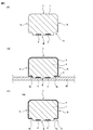
- FIGS. 3A and 3B are cross-sectional views illustrating steps performed in an example of a method for manufacturing the multilayer electronic component 100.
- 4 (C) to 4 (E) are continuations of FIG. 3 (B), and are cross-sectional views illustrating steps performed in an example of a method for manufacturing the multilayer electronic component 100.
- FIG. 1A is a front view of the multilayer electronic component 100 according to the first embodiment.
- FIG. 1B is a side view of the multilayer electronic component 100.
- FIG. 1C is a bottom
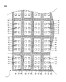
- FIG. 5 (F) to 5 (H) are continuations of FIG. 4 (E), and are cross-sectional views illustrating steps performed in an example of a method for manufacturing the multilayer electronic component 100. It is a bottom view (figure which shows a lower main surface) of the mother green sheet 11a shown to FIG. 3 (A).
- FIG. 7A is a cross-sectional view of the multilayer electronic component 200 according to the second embodiment viewed from the front direction.
- FIG. 7B is a cross-sectional view of the multilayer electronic component 200 viewed from the side surface direction.
- FIG. 8A is a cross-sectional view of the multilayer electronic component 300 according to the third embodiment viewed from the front direction.
- FIG. 8B is a cross-sectional view of the multilayer electronic component 300 viewed from the side surface direction.
- FIG. 9 is a perspective view of the multilayer electronic component 1100 disclosed in Patent Document 1.
- each embodiment shows an embodiment of the present invention by way of example, and the present invention is not limited to the content of the embodiment. Moreover, it is also possible to implement combining the content described in different embodiment, and the implementation content in that case is also included in this invention.
- the drawings are for helping the understanding of the specification, and may be schematically drawn, and the drawn components or the ratio of dimensions between the components are described in the specification. There are cases where the ratio of these dimensions does not match.
- the constituent elements described in the specification may be omitted in the drawings or may be drawn with the number omitted.
- FIGS. 2A and 2B show a multilayer electronic component 100 according to the first embodiment.
- 1A is a front view of the multilayer electronic component 100
- FIG. 1B is a side view of the multilayer electronic component 100
- FIG. 1C is a bottom view of the multilayer electronic component 100.
- 2A is a cross-sectional view of the multilayer electronic component 100 viewed from the front direction
- FIG. 2B is a cross-sectional view of the multilayer electronic component 100 viewed from the side surface direction.
- the multilayer electronic component 100 is, for example, a multilayer LC filter in which capacitors and inductors are formed and a predetermined filter circuit is configured.
- the type of the multilayer electronic component 100 is arbitrary and is not limited to the multilayer LC filter.
- the multilayer electronic component 100 includes a multilayer body 1 made of an insulator such as ceramic.
- the laminated body 1 has a rectangular parallelepiped shape, and includes a top surface T, a bottom surface B, and four side surfaces S. In the laminate 1, the surfaces are connected with rounded R shapes.
- the laminate 1 is formed by laminating a plurality of insulator layers made of ceramic or the like.
- via conductors are formed in predetermined portions so as to penetrate between both main surfaces.
- a conductor pattern having a predetermined shape is formed in a predetermined portion between layers of the predetermined insulator layer.
- Conductor patterns can be classified into capacitor conductor patterns, inductor conductor patterns, ground conductor patterns, and the like based on their functions.
- a capacitor is constituted by a capacitance formed between a pair of capacitor conductor patterns.
- an inductor is constituted by connecting a plurality of inductor conductor patterns with via conductors.
- the multilayer electronic component 100 is configured with a predetermined filter circuit by connecting capacitors and inductors formed inside the multilayer body 1.
- the via conductor and the conductor pattern are formed of a metal whose main component is silver or copper.
- a plurality of terminal electrodes 2 are formed on the bottom surface B of the laminate 1. Each of the terminal electrodes 2 is connected to a predetermined portion of a filter circuit configured inside the multilayer body 1. However, the terminal electrode 2 may include a so-called dummy electrode that is not connected to the filter circuit.
- the terminal electrode 2 is also made of a metal whose main component is silver or copper.
- a plating layer is formed on the surface of the terminal electrode 2.
- the first layer is formed of nickel
- the second layer is formed of one metal selected from gold, copper, and tin.
- the plating layer may have a single layer structure instead of a multilayer structure.
- the material of a plating layer is also arbitrary and may be formed with another metal.
- a step 3 is formed in an annular and rectangular shape.
- the step 3 is formed by two surfaces, a surface parallel to the bottom surface B and a surface parallel to the side surface S.
- the shield film 4 is formed on the top surface T and the four side surfaces S of the laminate 1.
- the shield film 4 is for suppressing noise from entering the inside of the multilayer electronic component 100 from the outside and suppressing leakage of noise from the inside of the multilayer electronic component 100 to the outside.
- the structure and material of the shield film 4 are arbitrary, but in this embodiment, the shield film 4 is formed in a multilayer structure by repeating sputtering a plurality of times.
- the shield film 4 can have a two-layer structure in which the first layer is copper and the second layer is SUS (stainless steel).
- a two-layer structure in which the first layer is copper and the second layer is nickel can be used.
- a three-layer structure in which the first layer is SUS, the second layer is copper, and the third layer is SUS can be employed.
- a three-layer structure in which the first layer is copper, the second layer is nickel, and the third layer is SUS can be employed.
- a three-layer structure in which the first layer is nickel, the second layer is copper, and the third layer is SUS can be used.
- a three-layer structure in which the first layer is SUS, the second layer is copper, and the third layer is nickel can be used.
- a plating layer is formed on the surface of the shield film 4.
- the first layer is formed of nickel
- the second layer is formed of one metal selected from gold, copper, and tin.
- the plating layer may have a single layer structure instead of a multilayer structure.
- the material of a plating layer is also arbitrary and may be formed with another metal.
- the shield film 4 is preferably connected to the ground via at least one terminal electrode 2.
- the portion of the edge 4 a of the shield film 4 is disposed inside the step 3.
- the shield film 4 is difficult to peel from the multilayer body 1. That is, in the multilayer electronic component 100, the edge 4a portion of the shield film 4 that is likely to be a starting point of peeling is disposed and protected inside the step 3, and other objects (such as other multilayer electronic components 100) are protected. The shield film 4 is difficult to peel from the laminate 1 because it is difficult to collide.
- the surfaces of the multilayer body 1 are connected with a rounded R shape. Therefore, the multilayer electronic component 100 is less likely to be cracked or chipped from the ridge line portion of the multilayer body 1 when another object (such as another multilayer electronic component) hits the ridge line portion of the multilayer body 1. Also, the multilayer electronic component 100 has a small impact on the other party when the ridge line portion of the multilayer body 1 hits another object (such as another multilayer electronic component).
- the multilayer electronic component 100 can be manufactured, for example, by the following method. This will be described with reference to FIGS. 3A to 5H and FIG.
- a plurality of mother green sheets 11a to 11k for preparing the laminate 1 are prepared.
- Each of the mother green sheets 11a to 11k is made up of a large number of green sheets arranged in a matrix so that a large number of laminated electronic components 100 can be manufactured together.
- terminal electrodes 2 are formed on the lower main surface of each green sheet of the mother green sheet 11a stacked in the lowermost layer.
- a conductive paste 12 for printing is preliminarily printed in a predetermined shape on a predetermined portion.
- a resin paste 13 for forming the step 3 is collectively put on the lower main surface of each green sheet of the mother green sheet 11a in a batch of all the conductive pastes 12 printed on the green sheet in advance. It is printed in an annular and rectangular shape to surround it. As a result, on the lower main surface of the mother green sheet 11a, the resin paste 13 is disposed along the outer peripheral edge of each green sheet so as to divide the individual green sheets arranged adjacent to each other in the vertical direction and the horizontal direction. Printed. At this stage, the resin pastes 13 printed on the adjacent green sheets are connected to each other.
- each green sheet of the mother green sheets 11a to 11j is formed with a hole penetrating between both main surfaces in a predetermined portion in advance in order to form a via conductor.
- the inside of the hole is filled with a conductive paste.
- the green sheets of the mother green sheets 11a to 11j are provided with a conductive paste in advance on a predetermined portion of the main surface as necessary in order to form a conductor pattern. It is printed in a predetermined shape.
- Each green sheet of the mother green sheet 11k laminated on the uppermost layer is a protective layer, no holes are formed, and no conductive paste is printed.
- mother green sheets 11a to 11k are laminated.
- the mother green sheets 11a to 11k are pressurized from above and below to be integrated, and the mother unfired laminate 11 is produced.
- both the conductive paste 12 and the resin paste 13 printed on the lower main surface of the mother green sheet 11 a are pushed into the bottom surface of the mother unfired laminate 11.
- the mother unfired laminate 11 is divided into individual unfired laminates 1 '.
- the division is performed, for example, by cutting with a dicer.
- the unfired laminate 1 ' is barrel-polished.
- an R-shaped roundness is formed at a portion where the surface of the unfired laminated body 1 ′ is in contact with the surface.
- an R-shaped roundness is also formed in the resin paste 13 pushed into the bottom surface of the unfired laminate 1 ′.
- FIG. 4E shows a different scale from FIG. 3A to FIG. 4D.
- the unfired laminated body 1 ′ is fired with a predetermined profile to produce the laminated body 1.
- a conductive paste (not shown) filled in the holes formed through the main surfaces of the mother green sheets 11a to 11j is printed on the main surfaces of the mother green sheets 11a to 11j.
- the conductive paste (not shown) that has been fired is also fired at the same time, and a via conductor and a conductor pattern are formed inside the laminate 1.
- the conductive paste 12 that has been pushed into the bottom surface of the unfired laminate 1 ′ is also fired simultaneously, and the terminal electrode 2 is formed on the bottom surface B of the laminate 1.
- the resin paste 13 that has been pushed into the bottom surface of the unfired laminated body 1 ′ is burned away, and a step 3 is formed on the ridgeline where the bottom surface B and the side surface S of the laminated body 1 are in contact.
- the step 3 is formed in an annular and rectangular shape.
- the bottom surface B of the multilayer body 1 is fixed to a fixing jig 50 having adhesiveness on the surface, and then the surface of the multilayer body 1 is sputtered to obtain the multilayer body 1.
- the shield film 4 is formed on the top surface T and the four side surfaces S. At this time, by providing a gap between the surface of the fixing jig 50 and the step 3, the portion of the edge 4 a of the shield film 4 is disposed inside the step 3.
- the laminated body 1 is removed from the fixing jig 50, and subsequently, plating layers are formed on the surfaces of the terminal electrode 2 and the shield film 4 by, for example, electrolytic plating.
- the mold electronic component 100 is completed.
- the shield film 4 may be formed by performing surface sputtering of the laminate 1. In this case, the plating layer is not formed on the surface of the shield film 4, but if necessary, a plating layer may be formed on the surface of the shield film 4 by adding a process.
- FIG. 7A and 7B show a multilayer electronic component 200 according to the second embodiment.
- 7A is a cross-sectional view of the multilayer electronic component 200 viewed from the front direction
- FIG. 7B is a cross-sectional view of the multilayer electronic component 200 viewed from the side surface direction.
- the multilayer electronic component 200 has changed a part of the configuration of the multilayer electronic component 100 according to the first embodiment.
- the step 3 is formed by two surfaces, a surface parallel to the bottom surface B and a surface parallel to the side surface S.
- the step 23 was formed in a staircase shape. That is, the step 23 has a structure in which a surface parallel to the bottom surface B, a surface parallel to the side surface S, another surface parallel to the bottom surface B, and another surface parallel to the side surface S are connected in this order. Consists of.
- step difference 23 being what was formed in cyclic
- the resin paste 13 that is formed in an annular and rectangular shape on the lower main surface of each green sheet of the mother green sheet 11 a that is stacked in the lowermost layer in the method for manufacturing the multilayer electronic component 100 described above.
- the step 23 can be formed in a step shape by forming it in a step shape by a method such as printing twice.
- the shield film 4 is a multilayer body because other objects (such as other multilayer electronic components 200) are less likely to collide with the edge 4 a portion of the shield film 4 that is likely to be a starting point of peeling. It is harder to peel from 1.
- FIG. 8A and 8B show a multilayer electronic component 300 according to the third embodiment.
- 8A is a cross-sectional view of the multilayer electronic component 300 viewed from the front direction
- FIG. 8B is a cross-sectional view of the multilayer electronic component 300 viewed from the side surface direction.
- the multilayer electronic component 300 also has a part of the configuration of the multilayer electronic component 100 according to the first embodiment. Specifically, in the multilayer electronic component 100, the shield film 4 is formed on the top surface T and the four side surfaces S of the multilayer body 1, but the multilayer electronic component 300 changes this, The shield film 34 was not formed on the top surface T of the laminate 1, but only on the four side surfaces S. In the multilayer electronic component 300, the internal shield film 35 is formed between the insulator layers in the vicinity of the top surface T of the multilayer body 1. The inner shield film 35 is connected to the shield film 34.
- the inner shield film 35 is obtained by printing a conductive paste for forming an inner shield film on the main surface of a green sheet (mother green sheet) laminated in the vicinity of the top surface T when the mother unfired laminate 11 is produced. It ’s fine.
- a mask may be formed in advance on the top surface T when the shield film 34 is formed by sputtering.
- the internal shield film 35 can be utilized for a circuit configuration (filter circuit configuration).
- a capacitor conductor pattern is formed between other layers adjacent to the insulating layer on which the inner shield film 35 is formed, and a capacitor formed between the capacitor conductor pattern and the inner shield film 35 causes a capacitor. (Shunt capacitor connected to the ground) can be configured.
- the shield film 34 is not formed on the top surface T of the multilayer body 1, but a shield film is also formed on the top surface T of the multilayer body 1 so as to coexist with the internal shield film 35.
- the shield films 4 and 34 are formed on the entire surface of the four side surfaces S of the multilayer body 1, but the shield films 4 and 34 are partially formed on the side surfaces S. It may be. Further, the shield films 4 and 34 do not need to be formed on the four side surfaces S, and may be formed on at least one side surface S.
- the steps 3 and 23 are formed in an annular shape on the ridgeline where the bottom surface B and the side surface S of the stacked body 1 are in contact, but the steps 3 and 23 are formed in an annular shape. It is not necessary, and it may be formed by being divided in the middle.
- multilayer electronic components 100, 200, and 300 are multilayer LC filters, but the type of the multilayer electronic component is arbitrary, and various other types of multilayer electronic components can be configured.
Landscapes
- Engineering & Computer Science (AREA)
- Power Engineering (AREA)
- Manufacturing & Machinery (AREA)
- Microelectronics & Electronic Packaging (AREA)
- Fixed Capacitors And Capacitor Manufacturing Machines (AREA)
- Ceramic Capacitors (AREA)
- Manufacturing Cores, Coils, And Magnets (AREA)
- Coils Or Transformers For Communication (AREA)
Abstract
シールド膜が積層体の表面から剥離しにくい積層型電子部品を提供する。 複数の絶縁体層が積層され、底面Bと、天面Tと、複数の側面Sとを備えた積層体1と、積層体1の側面Sに形成されたシールド膜4と、を備え、積層体1の底面Bと側面Sとが接する稜線に、少なくとも1つの段差3が形成され、シールド膜4の縁4aが、段差3の内部に配置されたものとする。すなわち、剥離の起点となりやすいシールド膜4の縁4aの部分を、段差3の内部に配置して保護する。
Description
本発明の積層型電子部品は、積層体の表面にシールド膜が形成された積層型電子部品に関し、さらに詳しくは、シールド膜が積層体の表面から剥離しにくい積層型電子部品に関する。
また、本発明の積層型電子部品の製造方法は、本発明の積層型電子部品を製造するのに適した積層型電子部品の製造方法に関する。
積層型電子部品において、外部から内部にノイズが侵入するのを抑制するとともに、内部から外部にノイズが漏洩するのを抑制するために、積層体の表面にシールド膜を形成する場合がある。
そのようなシールド膜を備えた積層型電子部品が、特許文献1(特開平9-121093号公報)に開示されている。図9に、特許文献1に開示された積層型電子部品(シールド型積層電子部品)1100を示す。
積層型電子部品1100は、直方体形状からなり、表面の所定の部分にシールド膜(GND電極)101が形成されている。
積層型電子部品1100には、表面からシールド膜101が容易に剥離してしまうという問題があった。たとえば、多数の積層型電子部品1100をパーツフィーダに入れて撹拌したような場合に、積層型電子部品1100同士がぶつかり合うことによって、表面からシールド膜101が容易に剥離してしまう場合があった。表面からシールド膜101が剥離した積層型電子部品1100は、たとえ剥離が部分的であったとしても、外観不良であり、また、電気的特性が変動してしまっている虞があり、さらに、剥離した部分が他の導電体に接触して短絡事故などが発生する虞があるため、使用することができなかった。
表面からのシールド膜101の剥離は、図9に、符号Xや符号Yで示す、シールド膜101の縁の部分を起点にして発生しやすい。シールド膜101の縁の部分は密着性が弱く、この部分に他の物(他の積層型電子部品1100など)がぶつかると、シールド膜101が容易に剥離してしまうからである。なお、剥離は、符号Xで示す、積層型電子部品1100の稜線部分のシールド膜101の縁の部分を起点にして、特に発生しやすい。稜線部分は、他の物(他の積層型電子部品1100など)がぶつかりやすく、かつ、シールド膜101の密着性が特に弱いからである。なお、図9における符号Xおよび符号Yは、本件出願人が、説明のために補足したものである。
本発明は、上述した従来の問題を解決するためになされたものであり、その手段として本発明の一局面にかかる積層型電子部品は、複数の絶縁体層が積層され、底面と、天面と、底面と天面とを繋ぐ複数の側面とを備えた積層体と、積層体の少なくとも1つの側面に形成されたシールド膜と、を備え、積層体の底面と側面とが接する稜線に、少なくとも1つの段差が形成され、シールド膜の縁の部分が、段差の内部に配置されたものとした。すなわち、本発明の積層型電子部品は、剥離の起点となりやすいシールド膜の縁の部分を、段差の内部に配置し、他の物(他の積層型電子部品など)がぶつからないようにして保護したものである。
たとえば、積層体が側面を4つ備え、シールド膜が、4つの側面に形成され、段差が、底面と4つの側面とが接する4つの稜線に、環状かつ矩形に形成されたものとすることが好ましい。この場合には、シールド膜によるノイズの侵入および漏洩の抑制を、より確実なものとすることができる。
シールド膜が、4つの側面の全面に形成されたものとすることが好ましい。この場合には、この場合には、シールド膜によるノイズの侵入および漏洩の抑制を、さらに確実なものとすることができる。
段差は、たとえば、側面に対して平行な面と、底面に対して平行な面との、2つの面で構成されたものとすることができる。あるいは、段差は、階段状に形成されたものとすることができる。これらの場合には、段差によって、シールド膜の縁の部分を確実に保護することができる。
積層体の、面と面とがR状の丸みを帯びて接続されていることが好ましい。この場合には、積層体の稜線部分に、他の物(他の積層型電子部品など)がぶつかった場合に、稜線部分から割れや欠けが発生するのを抑制することができる。また、積層体の稜線部分が、他の物(他の積層型電子部品など)にぶつかった場合に、相手に与える衝撃を緩和することができる。
シールド膜が、天面にも形成されていることが好ましい。この場合には、シールド膜によるノイズの侵入および漏洩の抑制を、より確実なものとすることができる。
シールド膜が、天面の全面に形成されていることが好ましい。この場合には、シールド膜によるノイズの侵入および漏洩の抑制を、さらに確実なものとすることができる。
積層体の、天面近傍の、絶縁体層の層間に、内部シールド膜を設けても良い。この場合には、内部シールド膜によって、ノイズの侵入および漏洩を抑制することができる。
本発明の積層型電子部品の製造方法は、本発明の積層型電子部品の製造に適したものである。本発明の一局面にかかる積層型電子部品の製造方法は、複数のセラミックグリーンシートが積層され、底面と、天面と、底面と天面とを繋ぐ複数の側面とを備え、底面の外周縁に沿って、樹脂ペーストが印刷された、未焼成積層体を用意する工程と、樹脂ペーストを、底面に押し込む工程と、未焼成積層体を焼成し、底面と側面とが接する稜線に、少なくとも1つの段差が形成された積層体を作製する工程と、積層体の側面に、縁の部分が段差の内部に配置されたシールド膜を形成する工程と、を順に備えるようにした。
未焼成積層体が、側面を4つ備え、樹脂ペーストが、未焼成積層体の、底面の外周縁に沿って、環状かつ矩形に印刷され、段差が、積層体の、底面と4つの側面とが接する4つの稜線に、環状かつ矩形に形成されることが好ましい。この場合には、シールド膜によるノイズの侵入および漏洩の抑制を、より確実なものとした積層型電子部品を作製することができる。
樹脂ペーストを底面に押し込む工程と、未焼成積層体を焼成して積層体を作製する工程との間に、さらに、未焼成積層体をバレル研磨し、未焼成積層体の、面と面とが接する部分に、R状の丸みを形成する工程を備えたものとすることが好ましい。この場合には、積層体の稜線部分に、他の物(他の積層型電子部品など)がぶつかった場合に、稜線部分から割れや欠けが発生するのを抑制することができる積層型電子部品を作製することができる。また、積層体の稜線部分が、他の物(他の積層型電子部品など)にぶつかった場合に、相手に与える衝撃が緩和された積層型電子部品を作製することができる。
未焼成積層体の底面の外周縁に沿って印刷された樹脂ペーストが、未焼成積層体の、最下層に積層されたセラミックグリーンシートの下側主面の外周縁に沿って予め印刷されたものであることが好ましい。この場合には、容易に、未焼成積層体の底面の外周縁に沿って樹脂ペーストを設けることができる。
シールド膜が、スパッタリングによって形成されることが好ましい。この場合には、容易に、品質の高いシールド膜を積層体の側面に形成し、シールド膜を段差の内部に達するものとすることができる。
本発明の積層型電子部品は、剥離の起点となりやすいシールド膜の縁の部分が、段差の内部に配置されて保護されており、他の物(他の積層型電子部品など)がぶつかりにくいため、シールド膜が積層体から剥離しにくい。
また、本発明の積層型電子部品の製造方法によれば、容易に、本発明の積層型電子部品を製造することができる。
以下、図面とともに、本発明を実施するための形態について説明する。
なお、各実施形態は、本発明の実施の形態を例示的に示したものであり、本発明が実施形態の内容に限定されることはない。また、異なる実施形態に記載された内容を組合せて実施することも可能であり、その場合の実施内容も本発明に含まれる。また、図面は、明細書の理解を助けるためのものであって、模式的に描画されている場合があり、描画された構成要素または構成要素間の寸法の比率が、明細書に記載されたそれらの寸法の比率と一致していない場合がある。また、明細書に記載されている構成要素が、図面において省略されている場合や、個数を省略して描画されている場合などがある。
[第1実施形態]
図1(A)~(C)、図2(A)、(B)に、第1実施形態にかかる積層型電子部品100を示す。ただし、図1(A)は積層型電子部品100の正面図、図1(B)は積層型電子部品100の側面図、図1(C)は積層型電子部品100の底面図である。また、図2(A)は正面方向から見た積層型電子部品100の断面図、図2(B)は側面方向から見た積層型電子部品100の断面図である。
図1(A)~(C)、図2(A)、(B)に、第1実施形態にかかる積層型電子部品100を示す。ただし、図1(A)は積層型電子部品100の正面図、図1(B)は積層型電子部品100の側面図、図1(C)は積層型電子部品100の底面図である。また、図2(A)は正面方向から見た積層型電子部品100の断面図、図2(B)は側面方向から見た積層型電子部品100の断面図である。
積層型電子部品100は、たとえば、内部にキャパシタやインダクタが形成され、所定のフィルタ回路が構成された積層型LCフィルタである。ただし、積層型電子部品100の種類は任意であり、積層型LCフィルタには限られない。
積層型電子部品100は、セラミックなどの絶縁体からなる積層体1を備えている。
積層体1は、直方体形状からなり、天面Tと、底面Bと、4つの側面Sとを備えている。積層体1は、面と面とが、R状の丸みを帯びて接続されている。
積層体1は、図示を省略しているが、セラミックなどからなる複数の絶縁体層が積層されたものからなる。所定の絶縁体層には、所定の部分に、両主面間を貫通してビア導体が形成されている。また、所定の絶縁体層の層間の所定の部分には、所定の形状の導体パターンが形成されている。導体パターンは、その機能から、キャパシタ導体パターン、インダクタ導体パターン、グランド導体パターンなどに分類することができる。そして、たとえば、1対のキャパシタ導体パターンの間に形成される容量によって、キャパシタが構成されている。また、たとえば、複数のインダクタ導体パターンをビア導体で繋ぐことによって、インダクタが構成されている。
積層型電子部品100は、積層体1の内部に形成されたキャパシタやインダクタを接続して、所定のフィルタ回路が構成されている。
ビア導体や、導体パターンは、銀や銅などを主成分とする金属によって形成されている。
積層体1の底面Bに、複数の端子電極2が形成されている。端子電極2は、それぞれ、積層体1の内部に構成されたフィルタ回路の所定の個所に接続されている。ただし、端子電極2のなかには、フィルタ回路に接続されない、いわゆるダミー電極が含まれている場合もある。
端子電極2も、銀や銅などを主成分とする金属によって形成されている。端子電極2の表面に、図示を省略しているが、めっき層が形成されている。めっき層は、たとえば、第1層がニッケルによって形成され、第2層が金、銅、錫から選ばれる1つの金属によって形成されている。ただし、めっき層は、多層構造ではなく、単層構造であっても良い。また、めっき層の材質も任意であり、他の金属によって形成されても良い。
積層体1の、底面Bと側面Sとが接する稜線に、環状かつ矩形に段差3が形成されている。段差3は、底面Bに平行な面と、側面Sに平行な面との、2つの面によって形成されている。
積層体1の、天面Tと、4つの側面Sに、シールド膜4が形成されている。シールド膜4は、外部から積層型電子部品100の内部にノイズが侵入するのを抑制するとともに、積層型電子部品100の内部から外部にノイズが漏洩するのを抑制するためのものである。シールド膜4の構造および材質は任意であるが、本実施形態においては、シールド膜4を、スパッタリングを複数回繰り返すことによって、多層構造に形成した。たとえば、シールド膜4は、第1層が銅、第2層がSUS(ステンレス鋼)の2層構造にすることができる。あるいは、第1層が銅、第2層がニッケルの2層構造にすることができる。あるいは、第1層がSUS、第2層が銅、第3層がSUSの3層構造にすることができる。あるいは、第1層が銅、第2層がニッケル、第3層がSUSの3層構造にすることができる。あるいは、第1層がニッケル、第2層が銅、第3層がSUSの3層構造にすることができる。あるいは、第1層がSUS、第2層が銅、第3層がニッケルの3層構造にすることができる。また、シールド膜4の表面に、図示を省略しているが、めっき層が形成されている。めっき層は、たとえば、第1層がニッケルによって形成され、第2層が金、銅、錫から選ばれる1つの金属によって形成されている。ただし、めっき層は、多層構造ではなく、単層構造であっても良い。また、めっき層の材質も任意であり、他の金属によって形成されても良い。
なお、シールド膜4は、少なくとも1つの端子電極2を経由して、グランドに接続されることが好ましい。
シールド膜4の縁4aの部分が、段差3の内部に配置されている。
積層型電子部品100は、シールド膜4の縁4aの部分が段差3の内部に配置されているため、シールド膜4が積層体1から剥離しにくい。すなわち、積層型電子部品100は、剥離の起点となりやすいシールド膜4の縁4aの部分が段差3の内部に配置されて保護されており、他の物(他の積層型電子部品100など)がぶつかりにくいため、シールド膜4が積層体1から剥離しにくい。
また、積層型電子部品100は、積層体1の、面と面とが、R状の丸みを帯びて接続されている。そのため、積層型電子部品100は、積層体1の稜線部分に、他の物(他の積層型電子部品など)がぶつかった場合に、積層体1の稜線部分から割れや欠けが発生しにくい。また、積層型電子部品100は、積層体1の稜線部分が、他の物(他の積層型電子部品など)にぶつかった場合に、相手に与える衝撃が小さい。
積層型電子部品100は、たとえば、次の方法によって製造することができる。図3(A)~図5(H)および図6を参照して説明する。
まず、図3(A)に示すように、積層体1を作製するための、複数のマザーグリーンシート11a~11kを用意する。マザーグリーンシート11a~11kは、それぞれ、多数の積層型電子部品100を一括して製造するように、多数個分のグリーンシートが、マトリックス状に配置されたものからなる。
図3(A)および図6(マザーグリーンシート11aの底面図)に示すように、最下層に積層されるマザーグリーンシート11aの個々のグリーンシートの下側主面には、端子電極2を形成するための導電性ペースト12が、予め、所定の部分に、所定の形状に印刷されている。
また、マザーグリーンシート11aの個々のグリーンシートの下側主面には、段差3を形成するための樹脂ペースト13が、予め、当該グリーンシートに印刷された全ての導電性ペースト12を一括して囲むように、環状かつ矩形に印刷されている。この結果、マザーグリーンシート11aの下側主面には、縦方向および横方向に隣接して配置された個々のグリーンシートを区切るように、個々のグリーンシートの外周縁に沿って樹脂ペースト13が印刷される。なお、この段階では、隣接する個々のグリーンシートに印刷された樹脂ペースト13同士が繋がった状態になっている。
マザーグリーンシート11a~11jの個々のグリーンシートには、図示を省略するが、ビア導体を形成するために、必要に応じて、予め、所定の部分に両主面間を貫通した孔が形成され、孔の内部に導電性ペーストが充填されている。また、マザーグリーンシート11a~11jの個々のグリーンシートには、同じく図示を省略するが、導体パターンを形成するために、必要に応じて、予め、主面の所定の部分に、導電性ペーストが所定の形状に印刷されている。
最上層に積層されるマザーグリーンシート11kの個々のグリーンシートは、保護層であり、孔は形成されず、導電性ペーストも印刷されていない。
次に、図3(B)に示すように、マザーグリーンシート11a~11kを積層する。
次に、図4(C)に示すように、マザーグリーンシート11a~11kを上下方向から加圧して、一体化させ、マザー未焼成積層体11を作製する。この結果、マザーグリーンシート11aの下側主面に印刷された、導電性ペースト12と、樹脂ペースト13とが、いずれも、マザー未焼成積層体11の底面に押し込まれる。
次に、図4(D)に示すように、マザー未焼成積層体11を、個々の未焼成積層体1’に分割する。分割は、たとえば、ダイサーで切ることによっておこなう。
次に、図4(E)に示すように、未焼成積層体1’をバレル研磨する。この結果、未焼成積層体1’の面と面とが接する部分に、R状の丸みが形成される。なお、未焼成積層体1’の底面に押し込まれた樹脂ペースト13にも、R状の丸みが形成される。なお、図4(E)は、図3(A)~図4(D)と、縮尺を変更して示している。
次に、図5(F)に示すように、未焼成積層体1’を、所定のプロファイルで焼成し、積層体1を作製する。この結果、マザーグリーンシート11a~11jの両主面間を貫通して形成された孔の内部に充填されていた導電性ペースト(図示せず)、マザーグリーンシート11a~11jの主面に印刷されていた導電性ペースト(図示せず)も同時に焼成され、積層体1の内部にビア導体と導体パターンとが形成される。また、未焼成積層体1’の底面に押し込まれていた導電性ペースト12も同時に焼成され、積層体1の底面Bに、端子電極2が形成される。さらに、未焼成積層体1’の底面に押し込まれていた樹脂ペースト13が焼失し、積層体1の底面Bと側面Sとが接する稜線に段差3が形成される。上述したように、段差3は、環状かつ矩形に形成される。
次に、図5(G)に示すように、積層体1の底面Bを、表面に粘着性を有する固定治具50に固定した上で、積層体1の表面にスパッタリングを施し、積層体1の天面Tと4つの側面Sにシールド膜4を形成する。このとき、固定治具50の表面と段差3との間に空隙を設けておくことにより、シールド膜4の縁4aの部分が段差3の内部に配置される。
最後に、図5(H)に示すように、積層体1を固定治具50から取り外し、続いて、たとえば電解めっきにより、端子電極2およびシールド膜4の表面にめっき層を形成して、積層型電子部品100を完成させる。
なお、上記製造方法においては、図5(G)に示すように、積層体1の表面にスパッタリングを施してシールド膜4を形成した後に、図5(F)に示すように、たとえば電解めっきにより、端子電極2およびシールド膜4の表面にめっき層を形成しているが、この順番を入れ替えても良い。すなわち、たとえば電解めっきにより、先に端子電極2の表面にめっき層を形成した後に、積層体1の表面スパッタリングを施してシールド膜4を形成するようにしても良い。この場合には、シールド膜4の表面にめっき層は形成されないが、必要であれば、工程を追加して、シールド膜4の表面にめっき層を形成しても良い。
[第2実施形態]
図7(A)、(B)に、第2実施形態にかかる積層型電子部品200を示す。ただし、図7(A)は正面方向から見た積層型電子部品200の断面図、図7(B)は側面方向から見た積層型電子部品200の断面図である。
図7(A)、(B)に、第2実施形態にかかる積層型電子部品200を示す。ただし、図7(A)は正面方向から見た積層型電子部品200の断面図、図7(B)は側面方向から見た積層型電子部品200の断面図である。
積層型電子部品200は、実施形態1にかかる積層型電子部品100の構成の一部を変更した。具体的には、積層型電子部品100では、段差3が、底面Bに平行な面と、側面Sに平行な面との、2つの面によって形成されていたが、積層型電子部品200は、これを変更し、段差23を、階段状に形成した。すなわち、段差23は、底面Bに平行な面と、側面Sに平行な面と、底面Bに平行なもう1つの面と、側面Sに平行なもう1つの面とが、この順に繋がった構造からなる。なお、段差23が、積層体1の、底面Bと側面Sとが接する稜線に、環状かつ矩形に形成されたものであることについては、変更はない。
積層型電子部品200は、上述した積層型電子部品100の製造方法において、最下層に積層されるマザーグリーンシート11aの個々のグリーンシートの下側主面に環状かつ矩形に形成する樹脂ペースト13を、2度にわたって印刷するなどの方法により、階段状に形成しておくことによって、段差23を階段状に形成することができる。
積層型電子部品200は、剥離の起点となりやすいシールド膜4の縁4aの部分に、他の物(他の積層型電子部品200など)がよりぶつかりにくくなっているため、シールド膜4が積層体1からより剥離しにくい。
[第3実施形態]
図8(A)、(B)に、第3実施形態にかかる積層型電子部品300を示す。ただし、図8(A)は正面方向から見た積層型電子部品300の断面図、図8(B)は側面方向から見た積層型電子部品300の断面図である。
図8(A)、(B)に、第3実施形態にかかる積層型電子部品300を示す。ただし、図8(A)は正面方向から見た積層型電子部品300の断面図、図8(B)は側面方向から見た積層型電子部品300の断面図である。
積層型電子部品300も、実施形態1にかかる積層型電子部品100の構成の一部を変更した。具体的には、積層型電子部品100では、シールド膜4を、積層体1の、天面Tと、4つの側面Sに形成していたが、積層型電子部品300は、これを変更し、シールド膜34を、積層体1の、天面Tには形成せず、4つの側面Sのみに形成した。また、積層型電子部品300は、積層体1の、天面T近傍の、絶縁体層の層間に、内部シールド膜35を形成した。内部シールド膜35は、シールド膜34に接続されている。
内部シールド膜35は、マザー未焼成積層体11を作製する際に、天面T近傍に積層されるグリーンシート(マザーグリーンシート)の主面に、内部シールド膜形成用の導電ペーストを印刷しておけば良い。また、天面Tにシールド膜34を非形成とするためには、シールド膜34をスパッタリングにより形成する際に、天面Tに予めマスクを形成しておけば良い。
積層型電子部品300は、内部シールド膜35を、回路構成(フィルタの回路構成)に活用することができる。たとえば、内部シールド膜35の形成された絶縁体層の層間に隣接する別の層間に、キャパシタ導体パターンを形成し、そのキャパシタ導体パターンと内部シールド膜35との間に形成される容量により、キャパシタ(グランドに接続されるシャントキャパシタ)を構成することができる。
なお、積層型電子部品300では、積層体1の天面Tにシールド膜34を形成しなかったが、積層体1の天面Tにもシールド膜を形成し、内部シールド膜35と併存させるようにしても良い。
以上、第1実施形態~第3実施形態にかかる積層型電子部品100、200、300について説明した。しかしながら、本発明が上述した内容に限定されることはなく、発明の趣旨に沿って、種々の変更をなすことができる。
たとえば、積層型電子部品100、200、300では、積層体1の4つの側面Sの全面に、シールド膜4、34を形成したが、シールド膜4、34は、側面Sに部分的に形成されたものであっても良い。また、シールド膜4、34は、4つの側面Sに形成される必要はなく、少なくとも1つの側面Sに形成されていれば良い。
また、積層型電子部品100、200、300では、段差3、23を、積層体1の、底面Bと側面Sとが接する稜線に環状に形成したが、段差3、23は環状に形成される必要はなく、途中で分断して形成されたものであっても良い。
また、積層型電子部品100、200、300は、積層型LCフィルタであったが、積層型電子部品の種類は任意であり、他の様々な種類の積層型電子部品を構成することができる。
1・・・積層体
2・・・端子電極
3、23・・・段差
4、34・・・シールド膜
4a・・・縁
1’・・・未焼成積層体
11・・・マザー未焼成積層体
11a~11k・・・マザーグリーンシート
12・・・導電性ペースト
13・・・樹脂ペースト
35・・・内部シールド膜
50・・・固定治具(表面に粘着性を有するもの)
2・・・端子電極
3、23・・・段差
4、34・・・シールド膜
4a・・・縁
1’・・・未焼成積層体
11・・・マザー未焼成積層体
11a~11k・・・マザーグリーンシート
12・・・導電性ペースト
13・・・樹脂ペースト
35・・・内部シールド膜
50・・・固定治具(表面に粘着性を有するもの)
Claims (14)
- 複数の絶縁体層が積層され、底面と、天面と、前記底面と前記天面とを繋ぐ複数の側面とを備えた積層体と、
前記積層体の少なくとも1つの側面に形成されたシールド膜と、を備えた積層型電子部品であって、
前記積層体の前記底面と前記側面とが接する稜線に、少なくとも1つの段差が形成され、
前記シールド膜の縁の部分が、前記段差の内部に配置された積層型電子部品。 - 前記積層体が、前記側面を4つ備え、
前記シールド膜が、4つの前記側面に形成され、
前記段差が、前記底面と4つの前記側面とが接する4つの前記稜線に、環状かつ矩形に形成された、請求項1に記載された積層型電子部品。 - 前記シールド膜が、4つの前記側面の全面に形成された、請求項2に記載された積層型電子部品。
- 前記段差が、前記側面に対して平行な面と、前記底面に対して平行な面との、2つの面で構成された、請求項1ないし3のいずれか1項に記載された積層型電子部品。
- 前記段差が、階段状に形成された、請求項1ないし3のいずれか1項に記載された積層型電子部品。
- 前記積層体の、面と面とがR状の丸みを帯びて接続されている、請求項1ないし5のいずれか1項に記載された積層型電子部品。
- 前記シールド膜が、前記天面にも形成された、請求項1ないし6のいずれか1項に記載された積層型電子部品。
- 前記シールド膜が、前記天面の全面に形成された、請求項7に記載された積層型電子部品。
- 前記積層体の、前記天面近傍の、前記絶縁体層の層間に、内部シールド膜を備えた、請求項1ないし8のいずれか1項に記載された積層型電子部品。
- 複数のセラミックグリーンシートが積層され、底面と、天面と、前記底面と前記天面とを繋ぐ複数の側面とを備え、前記底面の外周縁に沿って、樹脂ペーストが印刷された、未焼成積層体を用意する工程と、
前記樹脂ペーストを、前記底面に押し込む工程と、
前記未焼成積層体を焼成し、前記底面と前記側面とが接する稜線に、少なくとも1つの段差が形成された積層体を作製する工程と、
前記積層体の側面に、縁の部分が前記段差の内部に配置されたシールド膜を形成する工程と、を順に備えた積層型電子部品の製造方法。 - 前記未焼成積層体が、前記側面を4つ備え、
前記樹脂ペーストが、前記未焼成積層体の、前記底面の外周縁に沿って、環状かつ矩形に印刷され、
前記段差が、前記積層体の、前記底面と4つの前記側面とが接する4つの前記稜線に、環状かつ矩形に形成される、請求項10に記載された積層型電子部品の製造方法。 - 前記樹脂ペーストを前記底面に押し込む工程と、
前記未焼成積層体を焼成して前記積層体を作製する工程との間に、
さらに、前記未焼成積層体をバレル研磨し、前記未焼成積層体の、面と面とが接する部分に、R状の丸みを形成する工程を備えた、請求項10または11に記載された積層型電子部品の製造方法。 - 前記未焼成積層体の、前記底面の外周縁に沿って印刷された前記樹脂ペーストが、
前記未焼成積層体の、最下層に積層された前記セラミックグリーンシートの下側主面の外周縁に沿って予め印刷されたものである、請求項10ないし12のいずれか1項に記載された積層型電子部品の製造方法。 - 前記シールド膜が、スパッタリングによって形成される、請求項10ないし13のいずれか1項に記載された積層型電子部品の製造方法。
Priority Applications (3)
| Application Number | Priority Date | Filing Date | Title |
|---|---|---|---|
| CN201880014239.0A CN110366763B (zh) | 2017-02-28 | 2018-02-23 | 层叠型电子部件和层叠型电子部件的制造方法 |
| JP2019502956A JP6766946B2 (ja) | 2017-02-28 | 2018-02-23 | 積層型電子部品および積層型電子部品の製造方法 |
| US16/550,583 US10972066B2 (en) | 2017-02-28 | 2019-08-26 | Laminated electronic component and method of manufacturing the same |
Applications Claiming Priority (2)
| Application Number | Priority Date | Filing Date | Title |
|---|---|---|---|
| JP2017-037475 | 2017-02-28 | ||
| JP2017037475 | 2017-02-28 |
Related Child Applications (1)
| Application Number | Title | Priority Date | Filing Date |
|---|---|---|---|
| US16/550,583 Continuation US10972066B2 (en) | 2017-02-28 | 2019-08-26 | Laminated electronic component and method of manufacturing the same |
Publications (1)
| Publication Number | Publication Date |
|---|---|
| WO2018159481A1 true WO2018159481A1 (ja) | 2018-09-07 |
Family
ID=63370089
Family Applications (1)
| Application Number | Title | Priority Date | Filing Date |
|---|---|---|---|
| PCT/JP2018/006664 Ceased WO2018159481A1 (ja) | 2017-02-28 | 2018-02-23 | 積層型電子部品および積層型電子部品の製造方法 |
Country Status (4)
| Country | Link |
|---|---|
| US (1) | US10972066B2 (ja) |
| JP (1) | JP6766946B2 (ja) |
| CN (1) | CN110366763B (ja) |
| WO (1) | WO2018159481A1 (ja) |
Cited By (2)
| Publication number | Priority date | Publication date | Assignee | Title |
|---|---|---|---|---|
| WO2020184180A1 (ja) * | 2019-03-08 | 2020-09-17 | 株式会社村田製作所 | 電子部品の製造方法及び電子部品 |
| JP2023028128A (ja) * | 2021-08-18 | 2023-03-03 | Tdk株式会社 | コイル装置 |
Families Citing this family (8)
| Publication number | Priority date | Publication date | Assignee | Title |
|---|---|---|---|---|
| KR102019921B1 (ko) * | 2017-12-15 | 2019-09-11 | 주식회사 모다이노칩 | 파워 인덕터 및 그 제조 방법 |
| JP7233837B2 (ja) * | 2017-12-25 | 2023-03-07 | Tdk株式会社 | 電子部品の製造方法及び電子部品 |
| US11380478B2 (en) * | 2018-03-09 | 2022-07-05 | Samsung Electro-Mechanics Co., Ltd. | Coil component |
| KR102105385B1 (ko) * | 2018-07-18 | 2020-04-28 | 삼성전기주식회사 | 코일 부품 |
| KR102069635B1 (ko) * | 2018-09-06 | 2020-02-24 | 삼성전기주식회사 | 코일 부품 |
| KR102138885B1 (ko) * | 2018-09-20 | 2020-07-28 | 삼성전기주식회사 | 코일 부품 |
| CN112400210A (zh) * | 2020-10-12 | 2021-02-23 | 深圳顺络电子股份有限公司 | 一种层叠型屏蔽电感 |
| JP7609028B2 (ja) * | 2021-10-04 | 2025-01-07 | 株式会社村田製作所 | 積層セラミック電子部品 |
Citations (6)
| Publication number | Priority date | Publication date | Assignee | Title |
|---|---|---|---|---|
| JPH01295407A (ja) * | 1988-02-15 | 1989-11-29 | Murata Mfg Co Ltd | インダクター及びインダクターを含む複合部品並びにそれらの製造方法 |
| JPH0696992A (ja) * | 1992-07-27 | 1994-04-08 | Murata Mfg Co Ltd | 積層電子部品、その製造方法およびその特性測定方法 |
| JPH113836A (ja) * | 1997-06-11 | 1999-01-06 | Murata Mfg Co Ltd | 積層電子部品 |
| JPH11219837A (ja) * | 1998-02-02 | 1999-08-10 | Taiyo Yuden Co Ltd | 積層電子部品の製造方法 |
| JP2002305115A (ja) * | 2001-01-31 | 2002-10-18 | Matsushita Electric Ind Co Ltd | チップ型電子部品 |
| US20150364255A1 (en) * | 2014-06-13 | 2015-12-17 | Apple Inc. | Ceramic capacitors with built-in emi shield |
Family Cites Families (10)
| Publication number | Priority date | Publication date | Assignee | Title |
|---|---|---|---|---|
| US4918570A (en) * | 1988-12-20 | 1990-04-17 | Murata Manufacturing Co., Ltd. | Electronic component and its production method |
| EP0582881B1 (en) * | 1992-07-27 | 1997-12-29 | Murata Manufacturing Co., Ltd. | Multilayer electronic component, method of manufacturing the same and method of measuring characteristics thereof |
| JPH09121093A (ja) | 1995-10-25 | 1997-05-06 | Tdk Corp | シールド型積層電子部品 |
| MY122218A (en) | 1998-02-02 | 2006-03-31 | Taiyo Yuden Kk | Multilayer electronic component and manufacturing method therefor |
| JP2001189588A (ja) * | 1999-12-28 | 2001-07-10 | Tomio Yamaguchi | 電子部品、電子部品の電磁波シールド方法 |
| KR100780284B1 (ko) * | 2004-12-03 | 2007-11-28 | 삼성코닝 주식회사 | 플라즈마 표시 장치용 전면 필터 및 이를 포함하는플라즈마 표시 장치 |
| US7427801B2 (en) * | 2005-04-08 | 2008-09-23 | International Business Machines Corporation | Integrated circuit transformer devices for on-chip millimeter-wave applications |
| WO2007069789A1 (ja) * | 2005-12-16 | 2007-06-21 | Ibiden Co., Ltd. | 多層プリント配線板およびその製造方法 |
| CN103025137A (zh) * | 2011-09-26 | 2013-04-03 | 新科实业有限公司 | 电子部件模块及其制造方法 |
| CN110124193A (zh) * | 2019-05-05 | 2019-08-16 | 于毳 | 理疗控制电路 |
-
2018
- 2018-02-23 JP JP2019502956A patent/JP6766946B2/ja active Active
- 2018-02-23 CN CN201880014239.0A patent/CN110366763B/zh active Active
- 2018-02-23 WO PCT/JP2018/006664 patent/WO2018159481A1/ja not_active Ceased
-
2019
- 2019-08-26 US US16/550,583 patent/US10972066B2/en active Active
Patent Citations (6)
| Publication number | Priority date | Publication date | Assignee | Title |
|---|---|---|---|---|
| JPH01295407A (ja) * | 1988-02-15 | 1989-11-29 | Murata Mfg Co Ltd | インダクター及びインダクターを含む複合部品並びにそれらの製造方法 |
| JPH0696992A (ja) * | 1992-07-27 | 1994-04-08 | Murata Mfg Co Ltd | 積層電子部品、その製造方法およびその特性測定方法 |
| JPH113836A (ja) * | 1997-06-11 | 1999-01-06 | Murata Mfg Co Ltd | 積層電子部品 |
| JPH11219837A (ja) * | 1998-02-02 | 1999-08-10 | Taiyo Yuden Co Ltd | 積層電子部品の製造方法 |
| JP2002305115A (ja) * | 2001-01-31 | 2002-10-18 | Matsushita Electric Ind Co Ltd | チップ型電子部品 |
| US20150364255A1 (en) * | 2014-06-13 | 2015-12-17 | Apple Inc. | Ceramic capacitors with built-in emi shield |
Cited By (5)
| Publication number | Priority date | Publication date | Assignee | Title |
|---|---|---|---|---|
| WO2020184180A1 (ja) * | 2019-03-08 | 2020-09-17 | 株式会社村田製作所 | 電子部品の製造方法及び電子部品 |
| US11632883B2 (en) | 2019-03-08 | 2023-04-18 | Murata Manufacturing Co., Ltd. | Electronic component |
| JP2023028128A (ja) * | 2021-08-18 | 2023-03-03 | Tdk株式会社 | コイル装置 |
| JP7776279B2 (ja) | 2021-08-18 | 2025-11-26 | Tdk株式会社 | コイル装置 |
| US12518912B2 (en) | 2021-08-18 | 2026-01-06 | Tdk Corporation | Coil device |
Also Published As
| Publication number | Publication date |
|---|---|
| CN110366763B (zh) | 2023-02-28 |
| US10972066B2 (en) | 2021-04-06 |
| CN110366763A (zh) | 2019-10-22 |
| US20190379343A1 (en) | 2019-12-12 |
| JP6766946B2 (ja) | 2020-10-14 |
| JPWO2018159481A1 (ja) | 2019-12-19 |
Similar Documents
| Publication | Publication Date | Title |
|---|---|---|
| WO2018159481A1 (ja) | 積層型電子部品および積層型電子部品の製造方法 | |
| KR101939515B1 (ko) | 전자 부품 및 그 제조 방법 | |
| KR102267242B1 (ko) | 적층형 전자부품 및 적층형 전자부품의 제조 방법 | |
| US20120319537A1 (en) | Monolithic ceramic electronic component | |
| JP2015026760A (ja) | 積層コイル | |
| JP5852321B2 (ja) | 積層セラミックコンデンサ | |
| CN109565926B (zh) | 层叠电路基板、层叠电子部件和模块 | |
| US10079104B2 (en) | Capacitor | |
| US8922326B2 (en) | Laminated electronic component and method of manufacturing laminated electronic component | |
| WO2018159482A1 (ja) | 積層型電子部品および積層型電子部品の製造方法 | |
| JP2011151281A (ja) | 電子部品の製造方法 | |
| KR20130072531A (ko) | 적층 세라믹 전자부품 및 그 제조 방법 | |
| JP5278782B2 (ja) | 集合基板の製造方法 | |
| JP2004165375A (ja) | セラミック積層体の製法 | |
| JP2012089818A (ja) | 積層型セラミック電子部品の製造方法 | |
| WO2022044516A1 (ja) | 高周波電子部品 | |
| KR100749362B1 (ko) | 다층 배선 기판 형성에 이용되는 이재질부를 갖는 시트형성 방법 및 이재질부를 갖는 시트 | |
| JP2016048803A (ja) | 積層セラミックコンデンサ | |
| JP5831984B2 (ja) | 配線基板の製造方法 | |
| JP2006352018A (ja) | 積層型電子部品 | |
| JP2005032807A (ja) | 積層セラミック電子部品およびその製造方法 | |
| CN103404241B (zh) | 陶瓷多层基板及其制造方法 | |
| JP2006269829A (ja) | セラミック電子部品 | |
| KR100647021B1 (ko) | 전도성 비아를 구비한 저온동시소성세라믹 기판 및 그제조방법 | |
| JP2012109355A (ja) | 多層フェライト基板及び電子部品の製造方法 |
Legal Events
| Date | Code | Title | Description |
|---|---|---|---|
| 121 | Ep: the epo has been informed by wipo that ep was designated in this application |
Ref document number: 18760346 Country of ref document: EP Kind code of ref document: A1 |
|
| ENP | Entry into the national phase |
Ref document number: 2019502956 Country of ref document: JP Kind code of ref document: A |
|
| NENP | Non-entry into the national phase |
Ref country code: DE |
|
| 122 | Ep: pct application non-entry in european phase |
Ref document number: 18760346 Country of ref document: EP Kind code of ref document: A1 |