WO2018146813A1 - Module électronique - Google Patents
Module électronique Download PDFInfo
- Publication number
- WO2018146813A1 WO2018146813A1 PCT/JP2017/005147 JP2017005147W WO2018146813A1 WO 2018146813 A1 WO2018146813 A1 WO 2018146813A1 JP 2017005147 W JP2017005147 W JP 2017005147W WO 2018146813 A1 WO2018146813 A1 WO 2018146813A1
- Authority
- WO
- WIPO (PCT)
- Prior art keywords
- electronic
- coil
- electronic element
- insulating substrate
- connection body
- Prior art date
Links
Images


Classifications
-
- H—ELECTRICITY
- H01—ELECTRIC ELEMENTS
- H01L—SEMICONDUCTOR DEVICES NOT COVERED BY CLASS H10
- H01L23/00—Details of semiconductor or other solid state devices
- H01L23/34—Arrangements for cooling, heating, ventilating or temperature compensation ; Temperature sensing arrangements
- H01L23/36—Selection of materials, or shaping, to facilitate cooling or heating, e.g. heatsinks
-
- H—ELECTRICITY
- H01—ELECTRIC ELEMENTS
- H01L—SEMICONDUCTOR DEVICES NOT COVERED BY CLASS H10
- H01L23/00—Details of semiconductor or other solid state devices
- H01L23/12—Mountings, e.g. non-detachable insulating substrates
- H01L23/14—Mountings, e.g. non-detachable insulating substrates characterised by the material or its electrical properties
- H01L23/145—Organic substrates, e.g. plastic
-
- H—ELECTRICITY
- H01—ELECTRIC ELEMENTS
- H01L—SEMICONDUCTOR DEVICES NOT COVERED BY CLASS H10
- H01L23/00—Details of semiconductor or other solid state devices
- H01L23/34—Arrangements for cooling, heating, ventilating or temperature compensation ; Temperature sensing arrangements
- H01L23/36—Selection of materials, or shaping, to facilitate cooling or heating, e.g. heatsinks
- H01L23/367—Cooling facilitated by shape of device
- H01L23/3675—Cooling facilitated by shape of device characterised by the shape of the housing
-
- H—ELECTRICITY
- H01—ELECTRIC ELEMENTS
- H01L—SEMICONDUCTOR DEVICES NOT COVERED BY CLASS H10
- H01L23/00—Details of semiconductor or other solid state devices
- H01L23/34—Arrangements for cooling, heating, ventilating or temperature compensation ; Temperature sensing arrangements
- H01L23/36—Selection of materials, or shaping, to facilitate cooling or heating, e.g. heatsinks
- H01L23/373—Cooling facilitated by selection of materials for the device or materials for thermal expansion adaptation, e.g. carbon
- H01L23/3735—Laminates or multilayers, e.g. direct bond copper ceramic substrates
-
- H—ELECTRICITY
- H01—ELECTRIC ELEMENTS
- H01L—SEMICONDUCTOR DEVICES NOT COVERED BY CLASS H10
- H01L23/00—Details of semiconductor or other solid state devices
- H01L23/48—Arrangements for conducting electric current to or from the solid state body in operation, e.g. leads, terminal arrangements ; Selection of materials therefor
- H01L23/488—Arrangements for conducting electric current to or from the solid state body in operation, e.g. leads, terminal arrangements ; Selection of materials therefor consisting of soldered or bonded constructions
- H01L23/498—Leads, i.e. metallisations or lead-frames on insulating substrates, e.g. chip carriers
- H01L23/49838—Geometry or layout
-
- H—ELECTRICITY
- H01—ELECTRIC ELEMENTS
- H01L—SEMICONDUCTOR DEVICES NOT COVERED BY CLASS H10
- H01L23/00—Details of semiconductor or other solid state devices
- H01L23/52—Arrangements for conducting electric current within the device in operation from one component to another, i.e. interconnections, e.g. wires, lead frames
- H01L23/522—Arrangements for conducting electric current within the device in operation from one component to another, i.e. interconnections, e.g. wires, lead frames including external interconnections consisting of a multilayer structure of conductive and insulating layers inseparably formed on the semiconductor body
- H01L23/5227—Inductive arrangements or effects of, or between, wiring layers
-
- H—ELECTRICITY
- H01—ELECTRIC ELEMENTS
- H01L—SEMICONDUCTOR DEVICES NOT COVERED BY CLASS H10
- H01L23/00—Details of semiconductor or other solid state devices
- H01L23/552—Protection against radiation, e.g. light or electromagnetic waves
-
- H—ELECTRICITY
- H01—ELECTRIC ELEMENTS
- H01L—SEMICONDUCTOR DEVICES NOT COVERED BY CLASS H10
- H01L23/00—Details of semiconductor or other solid state devices
- H01L23/564—Details not otherwise provided for, e.g. protection against moisture
-
- H—ELECTRICITY
- H01—ELECTRIC ELEMENTS
- H01L—SEMICONDUCTOR DEVICES NOT COVERED BY CLASS H10
- H01L23/00—Details of semiconductor or other solid state devices
- H01L23/58—Structural electrical arrangements for semiconductor devices not otherwise provided for, e.g. in combination with batteries
- H01L23/64—Impedance arrangements
-
- H—ELECTRICITY
- H01—ELECTRIC ELEMENTS
- H01L—SEMICONDUCTOR DEVICES NOT COVERED BY CLASS H10
- H01L25/00—Assemblies consisting of a plurality of individual semiconductor or other solid state devices ; Multistep manufacturing processes thereof
-
- H—ELECTRICITY
- H01—ELECTRIC ELEMENTS
- H01L—SEMICONDUCTOR DEVICES NOT COVERED BY CLASS H10
- H01L25/00—Assemblies consisting of a plurality of individual semiconductor or other solid state devices ; Multistep manufacturing processes thereof
- H01L25/03—Assemblies consisting of a plurality of individual semiconductor or other solid state devices ; Multistep manufacturing processes thereof all the devices being of a type provided for in the same subgroup of groups H01L27/00 - H01L33/00, or in a single subclass of H10K, H10N, e.g. assemblies of rectifier diodes
- H01L25/04—Assemblies consisting of a plurality of individual semiconductor or other solid state devices ; Multistep manufacturing processes thereof all the devices being of a type provided for in the same subgroup of groups H01L27/00 - H01L33/00, or in a single subclass of H10K, H10N, e.g. assemblies of rectifier diodes the devices not having separate containers
- H01L25/07—Assemblies consisting of a plurality of individual semiconductor or other solid state devices ; Multistep manufacturing processes thereof all the devices being of a type provided for in the same subgroup of groups H01L27/00 - H01L33/00, or in a single subclass of H10K, H10N, e.g. assemblies of rectifier diodes the devices not having separate containers the devices being of a type provided for in group H01L29/00
- H01L25/072—Assemblies consisting of a plurality of individual semiconductor or other solid state devices ; Multistep manufacturing processes thereof all the devices being of a type provided for in the same subgroup of groups H01L27/00 - H01L33/00, or in a single subclass of H10K, H10N, e.g. assemblies of rectifier diodes the devices not having separate containers the devices being of a type provided for in group H01L29/00 the devices being arranged next to each other
-
- H—ELECTRICITY
- H01—ELECTRIC ELEMENTS
- H01L—SEMICONDUCTOR DEVICES NOT COVERED BY CLASS H10
- H01L25/00—Assemblies consisting of a plurality of individual semiconductor or other solid state devices ; Multistep manufacturing processes thereof
- H01L25/03—Assemblies consisting of a plurality of individual semiconductor or other solid state devices ; Multistep manufacturing processes thereof all the devices being of a type provided for in the same subgroup of groups H01L27/00 - H01L33/00, or in a single subclass of H10K, H10N, e.g. assemblies of rectifier diodes
- H01L25/10—Assemblies consisting of a plurality of individual semiconductor or other solid state devices ; Multistep manufacturing processes thereof all the devices being of a type provided for in the same subgroup of groups H01L27/00 - H01L33/00, or in a single subclass of H10K, H10N, e.g. assemblies of rectifier diodes the devices having separate containers
- H01L25/11—Assemblies consisting of a plurality of individual semiconductor or other solid state devices ; Multistep manufacturing processes thereof all the devices being of a type provided for in the same subgroup of groups H01L27/00 - H01L33/00, or in a single subclass of H10K, H10N, e.g. assemblies of rectifier diodes the devices having separate containers the devices being of a type provided for in group H01L29/00
- H01L25/117—Stacked arrangements of devices
-
- H—ELECTRICITY
- H01—ELECTRIC ELEMENTS
- H01L—SEMICONDUCTOR DEVICES NOT COVERED BY CLASS H10
- H01L28/00—Passive two-terminal components without a potential-jump or surface barrier for integrated circuits; Details thereof; Multistep manufacturing processes therefor
- H01L28/10—Inductors
-
- H—ELECTRICITY
- H02—GENERATION; CONVERSION OR DISTRIBUTION OF ELECTRIC POWER
- H02M—APPARATUS FOR CONVERSION BETWEEN AC AND AC, BETWEEN AC AND DC, OR BETWEEN DC AND DC, AND FOR USE WITH MAINS OR SIMILAR POWER SUPPLY SYSTEMS; CONVERSION OF DC OR AC INPUT POWER INTO SURGE OUTPUT POWER; CONTROL OR REGULATION THEREOF
- H02M1/00—Details of apparatus for conversion
- H02M1/44—Circuits or arrangements for compensating for electromagnetic interference in converters or inverters
-
- H—ELECTRICITY
- H02—GENERATION; CONVERSION OR DISTRIBUTION OF ELECTRIC POWER
- H02M—APPARATUS FOR CONVERSION BETWEEN AC AND AC, BETWEEN AC AND DC, OR BETWEEN DC AND DC, AND FOR USE WITH MAINS OR SIMILAR POWER SUPPLY SYSTEMS; CONVERSION OF DC OR AC INPUT POWER INTO SURGE OUTPUT POWER; CONTROL OR REGULATION THEREOF
- H02M7/00—Conversion of ac power input into dc power output; Conversion of dc power input into ac power output
- H02M7/003—Constructional details, e.g. physical layout, assembly, wiring or busbar connections
-
- H—ELECTRICITY
- H03—ELECTRONIC CIRCUITRY
- H03H—IMPEDANCE NETWORKS, e.g. RESONANT CIRCUITS; RESONATORS
- H03H1/00—Constructional details of impedance networks whose electrical mode of operation is not specified or applicable to more than one type of network
-
- H—ELECTRICITY
- H03—ELECTRONIC CIRCUITRY
- H03H—IMPEDANCE NETWORKS, e.g. RESONANT CIRCUITS; RESONATORS
- H03H7/00—Multiple-port networks comprising only passive electrical elements as network components
- H03H7/01—Frequency selective two-port networks
- H03H7/0115—Frequency selective two-port networks comprising only inductors and capacitors
-
- H—ELECTRICITY
- H05—ELECTRIC TECHNIQUES NOT OTHERWISE PROVIDED FOR
- H05K—PRINTED CIRCUITS; CASINGS OR CONSTRUCTIONAL DETAILS OF ELECTRIC APPARATUS; MANUFACTURE OF ASSEMBLAGES OF ELECTRICAL COMPONENTS
- H05K7/00—Constructional details common to different types of electric apparatus
- H05K7/14—Mounting supporting structure in casing or on frame or rack
- H05K7/1422—Printed circuit boards receptacles, e.g. stacked structures, electronic circuit modules or box like frames
- H05K7/1427—Housings
- H05K7/1432—Housings specially adapted for power drive units or power converters
- H05K7/14322—Housings specially adapted for power drive units or power converters wherein the control and power circuits of a power converter are arranged within the same casing
-
- H—ELECTRICITY
- H05—ELECTRIC TECHNIQUES NOT OTHERWISE PROVIDED FOR
- H05K—PRINTED CIRCUITS; CASINGS OR CONSTRUCTIONAL DETAILS OF ELECTRIC APPARATUS; MANUFACTURE OF ASSEMBLAGES OF ELECTRICAL COMPONENTS
- H05K7/00—Constructional details common to different types of electric apparatus
- H05K7/20—Modifications to facilitate cooling, ventilating, or heating
- H05K7/2089—Modifications to facilitate cooling, ventilating, or heating for power electronics, e.g. for inverters for controlling motor
- H05K7/209—Heat transfer by conduction from internal heat source to heat radiating structure
-
- H—ELECTRICITY
- H01—ELECTRIC ELEMENTS
- H01L—SEMICONDUCTOR DEVICES NOT COVERED BY CLASS H10
- H01L23/00—Details of semiconductor or other solid state devices
- H01L23/28—Encapsulations, e.g. encapsulating layers, coatings, e.g. for protection
- H01L23/31—Encapsulations, e.g. encapsulating layers, coatings, e.g. for protection characterised by the arrangement or shape
- H01L23/3107—Encapsulations, e.g. encapsulating layers, coatings, e.g. for protection characterised by the arrangement or shape the device being completely enclosed
- H01L23/3121—Encapsulations, e.g. encapsulating layers, coatings, e.g. for protection characterised by the arrangement or shape the device being completely enclosed a substrate forming part of the encapsulation
-
- H—ELECTRICITY
- H01—ELECTRIC ELEMENTS
- H01L—SEMICONDUCTOR DEVICES NOT COVERED BY CLASS H10
- H01L25/00—Assemblies consisting of a plurality of individual semiconductor or other solid state devices ; Multistep manufacturing processes thereof
- H01L25/03—Assemblies consisting of a plurality of individual semiconductor or other solid state devices ; Multistep manufacturing processes thereof all the devices being of a type provided for in the same subgroup of groups H01L27/00 - H01L33/00, or in a single subclass of H10K, H10N, e.g. assemblies of rectifier diodes
- H01L25/04—Assemblies consisting of a plurality of individual semiconductor or other solid state devices ; Multistep manufacturing processes thereof all the devices being of a type provided for in the same subgroup of groups H01L27/00 - H01L33/00, or in a single subclass of H10K, H10N, e.g. assemblies of rectifier diodes the devices not having separate containers
- H01L25/07—Assemblies consisting of a plurality of individual semiconductor or other solid state devices ; Multistep manufacturing processes thereof all the devices being of a type provided for in the same subgroup of groups H01L27/00 - H01L33/00, or in a single subclass of H10K, H10N, e.g. assemblies of rectifier diodes the devices not having separate containers the devices being of a type provided for in group H01L29/00
- H01L25/071—Assemblies consisting of a plurality of individual semiconductor or other solid state devices ; Multistep manufacturing processes thereof all the devices being of a type provided for in the same subgroup of groups H01L27/00 - H01L33/00, or in a single subclass of H10K, H10N, e.g. assemblies of rectifier diodes the devices not having separate containers the devices being of a type provided for in group H01L29/00 the devices being arranged next and on each other, i.e. mixed assemblies
-
- H—ELECTRICITY
- H01—ELECTRIC ELEMENTS
- H01L—SEMICONDUCTOR DEVICES NOT COVERED BY CLASS H10
- H01L25/00—Assemblies consisting of a plurality of individual semiconductor or other solid state devices ; Multistep manufacturing processes thereof
- H01L25/16—Assemblies consisting of a plurality of individual semiconductor or other solid state devices ; Multistep manufacturing processes thereof the devices being of types provided for in two or more different main groups of groups H01L27/00 - H01L33/00, or in a single subclass of H10K, H10N, e.g. forming hybrid circuits
- H01L25/162—Assemblies consisting of a plurality of individual semiconductor or other solid state devices ; Multistep manufacturing processes thereof the devices being of types provided for in two or more different main groups of groups H01L27/00 - H01L33/00, or in a single subclass of H10K, H10N, e.g. forming hybrid circuits the devices being mounted on two or more different substrates
-
- H—ELECTRICITY
- H03—ELECTRONIC CIRCUITRY
- H03H—IMPEDANCE NETWORKS, e.g. RESONANT CIRCUITS; RESONATORS
- H03H1/00—Constructional details of impedance networks whose electrical mode of operation is not specified or applicable to more than one type of network
- H03H2001/0021—Constructional details
- H03H2001/005—Wound, ring or feed-through type inductor
-
- H—ELECTRICITY
- H03—ELECTRONIC CIRCUITRY
- H03H—IMPEDANCE NETWORKS, e.g. RESONANT CIRCUITS; RESONATORS
- H03H1/00—Constructional details of impedance networks whose electrical mode of operation is not specified or applicable to more than one type of network
- H03H2001/0092—Inductor filters, i.e. inductors whose parasitic capacitance is of relevance to consider it as filter
Definitions
- the present invention relates to an electronic module.
- an electronic module such as a transfer power module is provided with a heat radiating plate (heat radiating layer) made of copper or the like on the back surface of the electronic module in order to cool a built-in electronic element or the like (for example, JP-A-2015-211152 reference).
- a heat radiating plate heat radiating layer
- the conductor layer, the insulating substrate, and the heat dissipation layer may serve as a capacitor (capacitor function may be formed).
- capacitor function When the capacitor function is formed in this way, noise due to the electronic elements in the electronic module may be emitted to the outside of the electronic module through the heat dissipation layer.
- the present invention provides an electronic module that can reduce noise.
- An electronic module includes: A first electronic unit comprising: a first insulating substrate; and a first electronic element provided on the first insulating substrate via a first conductor layer; A second electronic unit having a second insulating substrate, and a second electronic element provided on the second insulating substrate via a second conductor layer; A connection body provided between the first electronic unit and the second electronic unit; A coil wound around the connection body; May be provided.
- the first electronic element or the second electronic element may have a switching element.
- connection body may have a cylindrical shape.
- a cooling body is provided on the second insulating substrate side, and on the first insulating substrate side.
- the cooling body is not provided.
- the cooling body is provided on the first insulating substrate side, and the second insulating substrate side The cooling body may not be provided.
- An electronic module includes: You may further provide the resin substrate part which fixed the said connection body and the said coil.
- a controller for controlling the first electronic element or the second electronic element may be provided on the resin substrate part.
- connection body around which the coil is wound is provided between the first insulating substrate and the second insulating substrate,
- the first electronic element, the second electronic element, and the coil may not be electrically connected.
- connection body around which the coil is wound is provided between the first electronic element or the first conductor layer and the second electronic element or the second conductor layer, The first electronic element, the second electronic element, and the coil may be electrically connected.
- a coil wound around the connection body is incorporated. For this reason, generation
- FIG. 1 is a longitudinal sectional view of an electronic module according to an embodiment of the present invention.
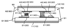
- FIG. 2 is a longitudinal sectional view of an electronic module according to another aspect of the embodiment of the present invention.
- FIG. 3 is a longitudinal sectional view of an electronic module according to still another aspect of the embodiment of the present invention.
- FIG. 4 is a longitudinal cross-sectional view of an electronic module according to an embodiment employing a resin substrate portion in the embodiment of the present invention.
- FIG. 5 is a longitudinal sectional view for explaining a modified example (modified example 1) of an aspect that can be used in the embodiment of the present invention.
- FIG. 6 is a longitudinal sectional view for explaining another modified example (modified examples 2 and 3) of the aspect that can be used in the embodiment of the present invention.
- FIG. 1 is a longitudinal sectional view of an electronic module according to an embodiment of the present invention.
- FIG. 2 is a longitudinal sectional view of an electronic module according to another aspect of the embodiment of the present invention.
- FIG. 3 is
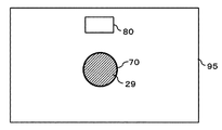
- FIG. 7 is a longitudinal sectional view showing a pseudo capacitor that can be formed by the electronic module according to the embodiment of the present invention.
- FIG. 8 is a circuit diagram showing a pseudo capacitor that can be formed by the electronic module according to the embodiment of the present invention in a mode in which the electronic element and the coil are not electrically connected.
- FIG. 9 is a circuit diagram showing a pseudo capacitor that can be formed by the electronic module according to the embodiment of the present invention in a mode in which the electronic element and the coil are electrically connected.
- FIG. 10 is a plan view showing a resin substrate portion that can be employed in the embodiment of the present invention.
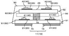
- FIG. 11 is a longitudinal cross-sectional view of an electronic module according to an aspect that employs a heat dissipation layer pattern in the embodiment of the present invention.
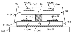
- the electronic module of this embodiment has a stack structure in which electronic elements 40 are stacked and arranged. More specifically, as shown in FIG. 1, the electronic module includes a first electronic unit 51, a second electronic unit 52, and a connection provided between the first electronic unit 51 and the second electronic unit 52. You may have the connection body 29 which consists of a pillar etc., and the coil 70 wound around the connection body 29.
- FIG. 1 the electronic module includes a first electronic unit 51, a second electronic unit 52, and a connection provided between the first electronic unit 51 and the second electronic unit 52. You may have the connection body 29 which consists of a pillar etc., and the coil 70 wound around the connection body 29.
- a semiconductor module can be cited as an example of the electronic module, and a semiconductor element can be cited as an example of the electronic element 40.
- the present invention is not limited to this, and a “semiconductor” is not necessarily used.
- the insulating substrate 60, the conductor layer 20, and the electronic element 40 may be covered with a sealing portion 90 made of a sealing resin or the like.
- the back surface of the sealing portion 90 may be at the same height as the back surface of the insulating substrate 60.
- the heat dissipation layer 10 is provided on the back surface of the insulating substrate 60, and the heat dissipation layer 10 protrudes from the back surface of the sealing portion 90.
- 60 may be embedded in the sealing portion 90, and the back surface of the heat dissipation layer 10 may be at the same height as the back surface of the sealing portion 90.
- the heat dissipation layer 10 may be provided on a cooling body 100 such as a heat sink.
- the electronic element 40 may include a switching element.
- the switching element include an FET such as a MOSFET, a bipolar transistor, and an IGBT.
- FET such as a MOSFET
- bipolar transistor such as a MOSFET
- IGBT an IGBT
- a typical example is a MOSFET.
- the first electronic unit 51 includes a first insulating substrate 61, a first conductor layer 21 provided on one side of the first insulating substrate 61 (upper side in FIG. 1), and one side of the first conductor layer 21. And the first electronic element 41 provided.
- the second electronic unit 52 may include the second conductor layer 22 and the second electronic element 42 provided on the second conductor layer 22.
- the second electronic unit 52 includes a second insulating substrate 62 provided on the other side (see FIG. 1, the lower side of FIG. 1) or one side (see FIG. 2, the upper side of FIG. 2) of the second electronic element 42. You may have.
- the second conductive layer 22 may be provided on the second insulating substrate 62, and the second electronic element 42 may be provided on the second conductive layer 22.
- the second electronic unit 52 includes a second insulating substrate 62, a second conductor layer 22 provided on one side of the second insulating substrate 62, and one side of the second conductor layer 22. And a second electronic element 42 provided in the device.
- the second electronic unit 52 includes a second insulating substrate 62, a second conductor layer 22 provided on the other side of the second insulating substrate 62, and the other side of the second conductor layer 22. And a second electronic element 42 provided in the device.
- the first electronic unit 51 may have the first heat radiation layer 11 provided on the other side (the lower side in FIG. 1) of the first insulating substrate 61.
- the second electronic unit 52 may include the second heat dissipation layer 12 provided on one side (the upper side in FIG. 2) of the second insulating substrate 62.
- the first electronic unit 51 includes the first heat dissipation layer 11 provided on the other side (the lower side of FIG. 3) of the first insulating substrate 61, and the second electrons
- the unit 52 may include the second heat dissipation layer 12 provided on one side (the upper side in FIG. 3) of the second insulating substrate 62.
- the first electronic element 41 and the second electronic element 42 may have a switching element and / or a control element that controls the switching element. Further, one of the first electronic element 41 and the second electronic element 42 may include only a switching element, and the other of the first electronic element 41 and the second electronic element 42 may include only a control element.
- the other electronic element 40 When one of the first electronic element 41 and the second electronic element 42 has a switching element and the other of the first electronic element 41 and the second electronic element 42 does not have a switching element, the other electronic element 40 Correspondingly, the heat dissipation layer 10 is provided, and the cooling body 100 is in contact with the heat dissipation layer 10, but the heat dissipation layer 10 corresponding to the one electronic element 40 is not provided, and the place corresponding to the one electronic element 40. May not be provided with a cooling body. For example, when the first electronic element 41 does not have a switching element and the second electronic element 42 has a switching element, the second heat dissipation layer 12 is not provided, but only the first heat dissipation layer 11 is provided.
- the first heat dissipation layer 11 may be in contact with the cooling body 100 (see FIG. 1).
- the first heat dissipation layer 11 is not provided, only the second heat dissipation layer 12 is provided, Only the layer 12 may abut against the cooling body 100 (see FIG. 2).
- the coil 70 may not be provided.
- connection body 29 may have a cylindrical shape.
- the coil 70 may be wound around each of the plurality of connection bodies 29, or the coil 70 may be wound around a part of the plurality of connection bodies 29. In the embodiment shown in FIG. 5, the coil 70 is wound around the left connection body 29, but the coil 70 is not wound around the right connection body 29.
- a plurality of first electronic elements 41 may be provided on the first insulating substrate 61.
- a plurality of second electronic elements 42 may be provided on the second insulating substrate 62.
- Each of the plurality of first electronic elements 41 and / or the plurality of second electronic elements 42 may be a switching element.
- connection body 29 around which the coil 70 is wound may be provided between the first insulating substrate 61 and the second insulating substrate 62.
- the first electronic element 41 and the second electronic element 42 and the coil 70 may not be electrically connected.
- a circuit including the coil 70 is a pseudo capacitor. It may be arranged virtually in parallel via (the stray capacitance of the substrate) (see also FIG. 7).
- the connection body 29 may be provided so as to connect the center portion in the surface direction of the first insulating substrate 61 and the center portion in the surface direction of the second insulating substrate 62.
- connection body 29 around which the coil 70 is wound may be provided between the conductor layers 20.
- a connection body 29 may be provided between the first conductor layer 21 and the second conductor layer 22, and the coil 70 may be wound around the connection body 29.
- connection body 29 around which the coil 70 is wound is provided between the electronic element 40 and the conductor layer 20.
- a connection body 29 may be provided between the first electronic element 41 and the second conductor layer 22, and the coil 70 may be wound around the connection body 29.
- the connection body 29 may be provided between the second electronic element 42 and the first conductor layer 21, and the coil 70 may be wound around the connection body 29.
- the connection body 29 around which the coil 70 is wound may be provided between the electronic element 40 and the conductor layer 20 (indicated by a broken line on the right side of FIG. 6).
- First electronic element 41 ).
- connection body 29 and the coil 70 may be provided.
- the connection body 29 and the coil 70 may be embedded in the resin substrate portion 95.
- thermoplastic resin is not particularly limited, but plastic or the like can be used.
- thermoplastic resin include polyethylene, polypropylene, poly-4-methylpentene-1, ionomer, polystyrene, AS resin, ABS resin, polyvinyl chloride, polyvinylidene chloride, methacrylic resin, polyvinyl alcohol, EVA, polycarbonate, and various types.
- thermosetting resin is not particularly limited, and examples thereof include an epoxy resin, a phenol resin, and an unsaturated polyester resin.
- the electronic element 40 when the electronic element 40 includes a switching element, noise generated from the switching element is passed through a capacitor formed in a pseudo manner by the heat dissipation layer 10, the conductor layer 20, the insulating substrate 60, and the like (see FIG. 7). , Will be discharged outside the electronic module. In the present embodiment, generation of noise can be suppressed by providing the coil 70 in the connection body 29.
- the terms “electronic element 40”, “first electronic element 41”, and “second electronic element 42” collectively refer to one or a plurality of electronic elements 40. Therefore, for example, “the electronic element 40 has a switching element” means that at least one of the electronic elements 40 is a switching element. The same applies to the first electronic element 41 and the second electronic element 42.
- a pseudo capacitor may be formed even in the insulating substrate 60 provided in the sealing portion 90, but by providing the coil 70 in the connection body 29, this is the case.
- the artificially formed capacitor can reduce the emission of noise to the outside of the electronic module (see FIG. 8).
- the heat dissipation layer 10 that contacts the cooling body 100 corresponding to only the other electronic element 40.
- the first heat dissipation layer 11 is provided as shown in FIG.
- the second electronic element 42 having a switching element is connected to the cooling body 100.
- a pseudo capacitor can be prevented from being formed (see FIG. 7). For this reason, it can reduce that noise is emitted outside the electronic module.
- the first electronic element 41 has a switching element and the second electronic element 42 does not have a switching element, as shown in FIG.
- a pseudo capacitor is formed between the cooling body 100 and the first electronic element 41 having the switching element. Can be prevented from being formed. For this reason, it can reduce that noise is emitted outside the electronic module.
- connection body 29 and the coil 70 are fixed, more specifically, a mode in which the connection body 29 and the coil 70 are embedded in the resin substrate portion 95 (see FIG. 10). Since the electronic module can be manufactured in a state where the connection body 29 and the coil 70 are positioned in advance, it can be expected that the manufacturing process is facilitated and the manufacturing cost is reduced.
- the connection body 29 around which the coil 70 is wound is provided between the first insulating substrate 61 and the second insulating substrate 62, the first insulating material is used. This is advantageous in that the noise caused by the first electronic element 41 provided on the conductive substrate 61 side and the second electronic element 42 provided on the second insulating substrate 62 side can be reduced by the coil 70.
- connection body 29 around which the coil 70 is wound is provided between the conductor layers 20, more specifically, the connection body around which the coil 70 is wound. 29 is employed between the first conductor layer 21 and the second conductor layer 22, noise generated from the adjacent first electronic element 41 and second electronic element 42 is generated by the coil 70. This is beneficial in that it can be reduced.
- a connection body 29 around which the coil 70 is wound may be provided corresponding to the switching element.
- the conductor layer 20 provided with the switching element and the conductor layer 20 provided with the switching element may be connected by a connection body 29 around which the coil 70 is wound.
- the conductor layer 20 provided with the switching element and the conductor layer 20 provided with the electronic element 40 (for example, a control element) that is not the switching element may be connected by the connection body 29 around which the coil 70 is wound.
- the coil 70 is more directly connected. This is advantageous in that noise can be reduced.
- connection body 29 around which the coil 70 is wound is employed between the electronic element 40 and the conductor layer 20, more specifically, the coil 70 is The wound connection body 29 is provided between the first electronic element 41 and the second conductor layer 22 and / or the connection body 29 around which the coil 70 is wound is the second electronic element 42 and the first conductor.
- the aspect provided between the layers 21 it is advantageous in that noise generated from the first electronic element 41 and the second electronic element 42 that are adjacent to each other can be reduced by the coil 70.
- a connection body 29 around which the coil 70 is wound may be provided corresponding to the switching element.
- the switching element and the conductor layer 20 provided with the switching element may be connected by a connection body 29 around which the coil 70 is wound.
- the switching element and the conductor layer 20 provided with the electronic element 40 that is not the switching element may be connected by the connection body 29 around which the coil 70 is wound.
- the connection body 29 around which the coil 70 is wound when a mode in which the switching element and the conductor layer 20 provided with the switching element are connected by the connection body 29 around which the coil 70 is wound is employed, it is advantageous in that noise can be reduced more directly by the coil 70. It is.
- connection body 29 around which the coil 70 is wound is employed between the electronic elements 40, more specifically, the connection body around which the coil 70 is wound. 29 is employed between the first electronic element 41 and the second electronic element 42, noise generated from the adjacent first electronic element 41 and the second electronic element 42 is generated by the coil 70. This is beneficial in that it can be reduced.
- a connection body 29 around which the coil 70 is wound may be provided corresponding to the switching element.
- the switching element and the switching element may be connected by a connection body 29 around which the coil 70 is wound.
- the switching element and the electronic element 40 (for example, the control element) that is not the switching element may be connected by the connection body 29 around which the coil 70 is wound.
- the connection body 29 around which the coil 70 is wound when a mode in which the switching element and the switching element are connected by the connection body 29 around which the coil 70 is wound is adopted, it is advantageous in that noise can be reduced more directly by the coil 70.
- the conductor layer 20 and the electronic element 40 are connected via the connection body 29 around which the coil 70 is wound, as compared with the case where the connection body 29 around which the coil 70 is wound is provided via the conductor layers 20.
- the noise caused by the coil 70 can be directly reduced when the above-described mode is adopted.
- the electronic elements 40 are directly connected by the connection body 29 around which the coil 70 is wound. In the case where the connected mode is adopted, the noise may be reduced more directly by the coil 70 in some cases.
- the control unit 80 in the case where the control unit 80 is provided in the resin substrate unit 95, the electronic element 40 and the control unit 80 can be positioned very close to each other. The possibility of this can be reduced. Further, by providing the control unit 80 in the electronic module as described above, an IPM (Intelligent Power Module) can be realized.
- IPM Intelligent Power Module
- the sealing portion 90 and the resin substrate portion 95 are formed of different resin materials, the resin substrate portion 95 located on the inner side and the sealing portion 90 located on the outer side have different functions. It is beneficial in that it can be fulfilled.
- the sealing portion 90 is a thermosetting resin
- high positioning accuracy can be expected when a thermoplastic resin is used as the material of the resin substrate portion 95. That is, when a thermosetting resin is used as the resin substrate portion 95, the hardness is not sufficient before heat is applied, so the positions of the coil 70, the connection body 29, the control portion 80, etc. are planned. There is a possibility of getting out of place.
- a thermoplastic resin is employed as the resin substrate portion 95, the hardness is sufficient before heat is applied, and therefore the possibility that the positions of the coil 70, the connection body 29, the control portion 80, and the like are shifted can be reduced. .
- the heat dissipation layer 10 has a plurality of heat dissipation layer patterns 15 partitioned in the surface direction.
- a heat dissipation layer pattern 15 By adopting such a heat dissipation layer pattern 15, the area in the in-plane direction of the heat dissipation layer 10 can be reduced, and a capacitor formed by the cooling body 100, the heat dissipation layer 10, the conductor layer 20, the insulating substrate 60 and the like. Capacitance in function (capacitor capacity) can be reduced. As a result, emitted noise can be suppressed.
- S the area of the parallel plate
- d the distance of the parallel plate
- ⁇ the dielectric of the insulator existing between the parallel plates
- FIG. 11 shows a mode in which the first heat dissipation layer 11 has the heat dissipation layer pattern 15, but is not limited to this, and instead of the first heat dissipation layer 11 or the first heat dissipation layer 11.
- the second heat dissipation layer 12 may have a heat dissipation layer pattern.
Landscapes
- Engineering & Computer Science (AREA)
- Power Engineering (AREA)
- Microelectronics & Electronic Packaging (AREA)
- Physics & Mathematics (AREA)
- Computer Hardware Design (AREA)
- Condensed Matter Physics & Semiconductors (AREA)
- General Physics & Mathematics (AREA)
- Chemical & Material Sciences (AREA)
- Materials Engineering (AREA)
- Electromagnetism (AREA)
- Ceramic Engineering (AREA)
- Thermal Sciences (AREA)
- Geometry (AREA)
- Health & Medical Sciences (AREA)
- Toxicology (AREA)
- Dc-Dc Converters (AREA)
- Coils Or Transformers For Communication (AREA)
Abstract
L'invention concerne un module électronique comprenant : une première unité électronique (51) pourvue d'un premier substrat isolant (61) et d'un premier élément électronique (41) disposé sur le premier substrat isolant (61) par le biais d'une première couche conductrice (21) ; une deuxième unité électronique (52) pourvue d'un deuxième substrat isolant (62) et d'un deuxième élément électronique (42) disposé sur le deuxième substrat isolant (62) par le biais d'une deuxième couche conductrice (22) ; un corps de connexion (29) disposé entre la première unité électronique (51) et la deuxième unité électronique (52) ; et une bobine (70) enroulée autour du corps de connexion (29).
Priority Applications (5)
| Application Number | Priority Date | Filing Date | Title |
|---|---|---|---|
| US15/763,925 US10770439B2 (en) | 2017-02-13 | 2017-02-13 | Electronic module |
| JP2017565321A JP6336688B1 (ja) | 2017-02-13 | 2017-02-13 | 電子モジュール |
| CN201780003898.XA CN108738369B (zh) | 2017-02-13 | 2017-02-13 | 电子模块 |
| PCT/JP2017/005147 WO2018146813A1 (fr) | 2017-02-13 | 2017-02-13 | Module électronique |
| NL2020394A NL2020394B1 (en) | 2017-02-13 | 2018-02-07 | Electronic module |
Applications Claiming Priority (1)
| Application Number | Priority Date | Filing Date | Title |
|---|---|---|---|
| PCT/JP2017/005147 WO2018146813A1 (fr) | 2017-02-13 | 2017-02-13 | Module électronique |
Publications (1)
| Publication Number | Publication Date |
|---|---|
| WO2018146813A1 true WO2018146813A1 (fr) | 2018-08-16 |
Family
ID=62487234
Family Applications (1)
| Application Number | Title | Priority Date | Filing Date |
|---|---|---|---|
| PCT/JP2017/005147 WO2018146813A1 (fr) | 2017-02-13 | 2017-02-13 | Module électronique |
Country Status (5)
| Country | Link |
|---|---|
| US (1) | US10770439B2 (fr) |
| JP (1) | JP6336688B1 (fr) |
| CN (1) | CN108738369B (fr) |
| NL (1) | NL2020394B1 (fr) |
| WO (1) | WO2018146813A1 (fr) |
Families Citing this family (1)
| Publication number | Priority date | Publication date | Assignee | Title |
|---|---|---|---|---|
| USD920937S1 (en) * | 2019-03-29 | 2021-06-01 | Shindengen Electric Manufacturing Co., Ltd. | Power module device containing semiconductor elements |
Citations (6)
| Publication number | Priority date | Publication date | Assignee | Title |
|---|---|---|---|---|
| JP2007005713A (ja) * | 2005-06-27 | 2007-01-11 | Toshiba Corp | 半導体装置 |
| JP2007234888A (ja) * | 2006-03-01 | 2007-09-13 | Oki Electric Ind Co Ltd | 部品内蔵基板の製造方法及びシステム基板 |
| JP2014033125A (ja) * | 2012-08-06 | 2014-02-20 | Toyota Motor Corp | 半導体装置及び半導体装置の製造方法 |
| JP2016510513A (ja) * | 2013-01-30 | 2016-04-07 | 日本テキサス・インスツルメンツ株式会社 | 回路アッセンブリ |
| WO2016103783A1 (fr) * | 2014-12-26 | 2016-06-30 | リンテック株式会社 | Feuille adhésive thermoconductrice, son procédé de fabrication et dispositif électronique l'utilisant |
| JP2017504211A (ja) * | 2014-01-14 | 2017-02-02 | クアルコム,インコーポレイテッド | スタック型導電性相互接続インダクタ |
Family Cites Families (18)
| Publication number | Priority date | Publication date | Assignee | Title |
|---|---|---|---|---|
| JPH06163270A (ja) * | 1992-11-19 | 1994-06-10 | Murata Mfg Co Ltd | 多層基板 |
| JP3575478B2 (ja) | 2002-07-03 | 2004-10-13 | ソニー株式会社 | モジュール基板装置の製造方法、高周波モジュール及びその製造方法 |
| US7613010B2 (en) * | 2004-02-02 | 2009-11-03 | Panasonic Corporation | Stereoscopic electronic circuit device, and relay board and relay frame used therein |
| JP4762531B2 (ja) * | 2004-11-30 | 2011-08-31 | 太陽誘電株式会社 | 電子部品及びその製造方法 |
| JP2009081325A (ja) * | 2007-09-27 | 2009-04-16 | Sanyo Electric Co Ltd | 回路装置 |
| US8482931B2 (en) * | 2008-12-24 | 2013-07-09 | Panasonic Corporation | Package structure |
| JP5496357B2 (ja) * | 2010-10-27 | 2014-05-21 | 三菱電機株式会社 | 電動パワーステアリング用モータ駆動制御装置 |
| WO2013002249A1 (fr) * | 2011-06-27 | 2013-01-03 | ローム株式会社 | Module à semi-conducteurs |
| JP5460653B2 (ja) * | 2011-07-14 | 2014-04-02 | 本田技研工業株式会社 | 半導体装置 |
| DE102012106615A1 (de) * | 2012-07-20 | 2014-01-23 | Sma Solar Technology Ag | Elektronische Baugruppe |
| JP6005438B2 (ja) * | 2012-08-10 | 2016-10-12 | 株式会社ThruChip Japan | 積層集積回路 |
| JP5788585B2 (ja) * | 2013-05-13 | 2015-09-30 | 新電元工業株式会社 | 電子モジュールおよびその製造方法 |
| WO2015005181A1 (fr) | 2013-07-08 | 2015-01-15 | 株式会社 村田製作所 | Élément de conversion de puissance |
| JP5867472B2 (ja) * | 2013-09-17 | 2016-02-24 | 株式会社安川電機 | 電力変換装置 |
| JP6269296B2 (ja) | 2014-04-25 | 2018-01-31 | 株式会社デンソー | 半導体モジュール |
| JP6237516B2 (ja) * | 2014-07-18 | 2017-11-29 | 株式会社デンソー | 電源装置 |
| JP6316708B2 (ja) * | 2014-08-26 | 2018-04-25 | ルネサスエレクトロニクス株式会社 | 半導体装置の製造方法 |
| CN105762130B (zh) * | 2014-12-15 | 2019-04-05 | 财团法人工业技术研究院 | 功率模块 |
-
2017
- 2017-02-13 JP JP2017565321A patent/JP6336688B1/ja active Active
- 2017-02-13 CN CN201780003898.XA patent/CN108738369B/zh active Active
- 2017-02-13 US US15/763,925 patent/US10770439B2/en active Active
- 2017-02-13 WO PCT/JP2017/005147 patent/WO2018146813A1/fr active Application Filing
-
2018
- 2018-02-07 NL NL2020394A patent/NL2020394B1/en active
Patent Citations (6)
| Publication number | Priority date | Publication date | Assignee | Title |
|---|---|---|---|---|
| JP2007005713A (ja) * | 2005-06-27 | 2007-01-11 | Toshiba Corp | 半導体装置 |
| JP2007234888A (ja) * | 2006-03-01 | 2007-09-13 | Oki Electric Ind Co Ltd | 部品内蔵基板の製造方法及びシステム基板 |
| JP2014033125A (ja) * | 2012-08-06 | 2014-02-20 | Toyota Motor Corp | 半導体装置及び半導体装置の製造方法 |
| JP2016510513A (ja) * | 2013-01-30 | 2016-04-07 | 日本テキサス・インスツルメンツ株式会社 | 回路アッセンブリ |
| JP2017504211A (ja) * | 2014-01-14 | 2017-02-02 | クアルコム,インコーポレイテッド | スタック型導電性相互接続インダクタ |
| WO2016103783A1 (fr) * | 2014-12-26 | 2016-06-30 | リンテック株式会社 | Feuille adhésive thermoconductrice, son procédé de fabrication et dispositif électronique l'utilisant |
Also Published As
| Publication number | Publication date |
|---|---|
| JP6336688B1 (ja) | 2018-06-06 |
| NL2020394A (en) | 2018-08-22 |
| US20190057956A1 (en) | 2019-02-21 |
| CN108738369A (zh) | 2018-11-02 |
| US10770439B2 (en) | 2020-09-08 |
| NL2020394B1 (en) | 2018-10-29 |
| CN108738369B (zh) | 2022-03-29 |
| JPWO2018146813A1 (ja) | 2019-02-14 |
Similar Documents
| Publication | Publication Date | Title |
|---|---|---|
| JP6827085B2 (ja) | 高電圧電力モジュール | |
| US9871463B2 (en) | Power module | |
| US10084389B2 (en) | Power module | |
| US20170317005A1 (en) | Electronic Component Having a Heat-Sink Thermally Coupled to a Heat-Spreader | |
| US20120147641A1 (en) | Switching device | |
| US10032688B2 (en) | Electronic component and method for dissipating heat from a semiconductor die | |
| US20150137697A1 (en) | Integrated light source driving circuit and light source module using the same | |
| US8754462B2 (en) | Semiconductor device | |
| JP6336688B1 (ja) | 電子モジュール | |
| ES2898791T3 (es) | Módulo de potencia | |
| US9978671B2 (en) | Power semiconductor device | |
| KR102460079B1 (ko) | 솔리드 스테이트 드라이브의 미디어 서버 모듈 | |
| US8823053B2 (en) | Semiconductor device including a plurality of first flat plates containing a material that absorbs an electromagnetic wave at a high frequency | |
| KR102016019B1 (ko) | 고열전도성 반도체 패키지 | |
| JP6240343B1 (ja) | 半導体装置及び半導体装置の製造方法 | |
| JP6236547B1 (ja) | 半導体装置及び半導体装置の製造方法 | |
| JP6494855B2 (ja) | 電子モジュール | |
| US11848146B2 (en) | Stacked electronic module and method to make the same | |
| KR20100127453A (ko) | 히트싱크를 갖는 기판보드 어셈블리 및 그 제조방법 | |
| US20150228567A1 (en) | Package substrate and semiconductor package using the same | |
| JP2015018608A (ja) | 発光装置 | |
| JP2015090924A (ja) | 半導体装置 |
Legal Events
| Date | Code | Title | Description |
|---|---|---|---|
| ENP | Entry into the national phase |
Ref document number: 2017565321 Country of ref document: JP Kind code of ref document: A |
|
| 121 | Ep: the epo has been informed by wipo that ep was designated in this application |
Ref document number: 17896099 Country of ref document: EP Kind code of ref document: A1 |
|
| NENP | Non-entry into the national phase |
Ref country code: DE |
|
| 122 | Ep: pct application non-entry in european phase |
Ref document number: 17896099 Country of ref document: EP Kind code of ref document: A1 |