WO2018127992A1 - 光ファイバアレイ及び光ファイバアレイの製造方法 - Google Patents
光ファイバアレイ及び光ファイバアレイの製造方法 Download PDFInfo
- Publication number
- WO2018127992A1 WO2018127992A1 PCT/JP2017/031048 JP2017031048W WO2018127992A1 WO 2018127992 A1 WO2018127992 A1 WO 2018127992A1 JP 2017031048 W JP2017031048 W JP 2017031048W WO 2018127992 A1 WO2018127992 A1 WO 2018127992A1
- Authority
- WO
- WIPO (PCT)
- Prior art keywords
- optical fiber
- fused
- groove
- fiber array
- fusion
- Prior art date
- Legal status (The legal status is an assumption and is not a legal conclusion. Google has not performed a legal analysis and makes no representation as to the accuracy of the status listed.)
- Ceased
Links
Images


Classifications
-
- G—PHYSICS
- G02—OPTICS
- G02B—OPTICAL ELEMENTS, SYSTEMS OR APPARATUS
- G02B6/00—Light guides; Structural details of arrangements comprising light guides and other optical elements, e.g. couplings
- G02B6/24—Coupling light guides
-
- G—PHYSICS
- G02—OPTICS
- G02B—OPTICAL ELEMENTS, SYSTEMS OR APPARATUS
- G02B6/00—Light guides; Structural details of arrangements comprising light guides and other optical elements, e.g. couplings
- G02B6/24—Coupling light guides
- G02B6/26—Optical coupling means
-
- G—PHYSICS
- G02—OPTICS
- G02B—OPTICAL ELEMENTS, SYSTEMS OR APPARATUS
- G02B6/00—Light guides; Structural details of arrangements comprising light guides and other optical elements, e.g. couplings
- G02B6/24—Coupling light guides
- G02B6/36—Mechanical coupling means
- G02B6/40—Mechanical coupling means having fibre bundle mating means
Definitions
- the present invention relates to an optical fiber array and a method for manufacturing the optical fiber array.
- optical fiber arrays are widely used as coupling elements for coupling optical transmission lines in optical communications, and are applied to optical waveguide splitters, optical switches, and the like.
- the optical fiber array has a structure in which optical fibers are arranged on a plurality of V-grooved substrates, and the optical fibers are sandwiched from above by a fixing member, and are fixed so that they have a very high density and high accuracy. Can be achieved.
- Patent Document 1 discloses an optical fiber array using a fused optical fiber having a fused portion formed by fusion-bonding two optical fibers, and a portion including the fused portion is formed on a substrate. It is described that they are arranged and fixed.
- optical fibers having different mode field diameters such as a high NA fiber and a single mode fiber, are connected by TEC fusion.
- the fused portion of the fused optical fiber may swell depending on the fused connection state.
- An object of some embodiments of the present invention is to provide an optical fiber array in which the alignment accuracy of fused optical fibers is improved.
- Some embodiments of the present invention include an optical fiber composed of a fused optical fiber having a fused portion formed by melting and connecting respective ends of two optical fibers, and the optical fiber.
- An optical fiber array comprising a substrate having an optical fiber groove portion having a groove to be disposed, and a fixing member that sandwiches and holds the optical fiber disposed in the optical fiber groove portion together with the substrate.
- An optical fiber array wherein an escape portion of the fusion part, which is a recess in which at least a part of the fusion part is located when an optical fiber is disposed in the optical fiber groove part, is formed. .
- the alignment accuracy of the fused optical fibers can be increased in the optical fiber array.
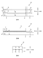
- FIG. 1A is a plan view of the optical fiber array 10 of the first embodiment.
- FIG. 1B is a left side view of the optical fiber array 10 of the first embodiment.
- FIG. 1C is a front view of the optical fiber array 10 of the first embodiment.
- FIG. 2 is a front view of the optical fiber array 10 according to a modification of the first embodiment.
- FIG. 3 is a flowchart of the method for manufacturing the optical fiber array 10.
- FIG. 4A is a plan view of the optical fiber array 10 of the second embodiment.
- FIG. 4B is a left side view of the optical fiber array 10 of the second embodiment.
- FIG. 4C is a front view of the optical fiber array 10 of the second embodiment.
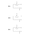
- 5A to 5C are cross-sectional views for explaining variations of the escape portion 5.
- An optical fiber composed of a fused optical fiber having a fused portion formed by melting and connecting respective end portions of two optical fibers, and an optical fiber groove portion having a groove for arranging the optical fiber.
- An optical fiber array comprising: a substrate; and a fixing member that sandwiches and holds the optical fiber disposed in the optical fiber groove together with the substrate, wherein the optical fiber is disposed in the optical fiber groove on the substrate.
- the optical fiber array is characterized in that an escape portion of the fusion part, which is a recess in which at least a part of the fusion part is located, is formed. According to such an optical fiber array, the alignment accuracy of the fused optical fibers can be increased.
- the fixing member is formed with a relief portion of the fusion portion, which is a recess where at least a part of the fusion portion is located when the fixing member abuts on the optical fiber.
- the alignment accuracy of the fused optical fiber can be increased.
- the depth of the escape portion is preferably larger than the diameter of the fused portion. Thereby, the alignment accuracy of the fused optical fiber can be increased.
- the escape portion is a V groove. Thereby, the alignment accuracy of the fused optical fiber can be increased.
- the escape portion is a U groove. Thereby, the alignment accuracy of the fused optical fiber can be increased.
- the two optical fibers have different diameters. Thereby, the alignment accuracy of the fused optical fiber can be increased.
- An optical fiber composed of a fused optical fiber having a fused portion formed by melting and connecting respective end portions of two optical fibers, and an optical fiber groove portion having a groove for arranging the optical fiber. And a fixing member that sandwiches and holds the optical fiber disposed in the optical fiber groove portion together with the substrate, wherein the optical fiber is on the optical fiber groove portion.
- a method of manufacturing an optical fiber array is provided, in which a relief portion of the fusion portion, which is a recess in which at least a part of the fusion portion is located, is formed. According to such an optical fiber array manufacturing method, the alignment accuracy of the fused optical fibers can be increased.
- FIG. 1A is a plan view of the optical fiber array 10 of the first embodiment.
- FIG. 1B is a left side view of the optical fiber array 10 of the first embodiment.
- FIG. 1C is a front view of the optical fiber array 10 of the first embodiment.
- the adhesive is not shown. In order to simplify the drawing, the number of optical fibers may be reduced for illustration.
- each direction is defined as shown in FIGS. 1A to 1C. That is, the direction of the optical fiber groove 4a and the optical fiber groove 4b of the optical fiber array 10 (the optical axis direction of the optical fiber 1a and the optical fiber 1b) is defined as “front-rear direction”, and the side of the optical fiber array end face 8 is defined as “front”.
- the reverse side (the side of the optical fiber 1a extending from the optical fiber array 10) is referred to as “rear”.
- the direction in which the plurality of optical fiber grooves 4a (or the plurality of optical fiber grooves 4b) are arranged is referred to as “left-right direction”. Further, the thickness direction of the optical fiber array 10 is referred to as “vertical direction”.
- the optical fiber array 10 is a coupling element that couples optical transmission lines.
- the optical fiber array 10 includes an optical fiber 1 a and an optical fiber 1 b, a substrate 2, and a fixing member 3.
- the optical fiber 1a and the optical fiber 1b, the substrate 2 and the fixing member 3 are bonded by an adhesive (not shown).
- the optical fiber 1a and the optical fiber 1b are optical fibers in which the optical fiber 1a and the optical fiber 1b are fusion-bonded by TEC fusion.
- an optical fiber fusion-bonded by TEC fusion may be simply referred to as a “fusion optical fiber”.
- the optical fiber 1a and the optical fiber 1b that are fusion-bonded by TEC fusion may be referred to as a fusion optical fiber 1.
- the optical fiber array 10 includes two fused optical fibers 1.
- the number of the fused optical fibers 1 is not limited to this, and may be one or three or more.
- an optical fiber groove 4a and an optical fiber groove 4b which will be described later, may be formed according to the number of the fused optical fibers 1.
- the fused optical fiber 1 of this embodiment has shown the example fused by the optical fiber 1a and the optical fiber 1b with the same diameter.
- TEC fusion is a technique for fusion-connecting optical fibers having different core mode field diameters, such as fusion connection of high NA fiber and single mode fiber.
- heat treatment is performed with a gas burner or the like to diffuse the mode field diameter of the core of one optical fiber so that the mode field diameter of one optical fiber gradually matches the mode field diameter of the other optical fiber.
- the fused portion may swell compared to the diameter of the optical fiber.
- the fused optical fiber 1 shown in FIGS. 1A and 1B has a fused portion 6 that is a fused portion.
- the fused portion 6 is a fused portion that swells compared to the diameter of the optical fiber 1a and the optical fiber 1b due to fusion-bonding by TEC fusion between the optical fiber 1a and the optical fiber 1b.
- the substrate 2 is a member for arranging the fused optical fiber 1.
- the substrate 2 has a plurality of optical fiber grooves 4a and a plurality of optical fiber grooves 4b.
- Each optical fiber groove 4a and each optical fiber groove 4b are V-shaped grooves along the front-rear direction.
- the plurality of optical fiber grooves 4a (or the plurality of optical fiber grooves 4b) are arranged side by side in the left-right direction.
- Each fused optical fiber 1 is supported and arranged by the optical fiber groove 4a and the optical fiber groove 4b of the substrate 2, respectively.
- a relief portion 5 is formed on the substrate 2.
- the escape portion 5 is for allowing the portion of the fusion portion 6 that is larger than the diameter of the fused optical fiber 1 to escape into the space formed by the escape portion 5 without contacting the optical fiber groove 4a and the optical fiber groove 4b. It is a recess. 1A and 1B is formed on the substrate 2 so as to extend in the left-right direction. Further, the escape portion 5 is a V-groove along the left-right direction. The depth of the V groove of the escape portion 5 is larger than the diameter of the fused portion 6.
- the diameter of the fused part 6 means the length from the center of the part where the fused part 6 swells most.
- the depth of the V-groove of the escape portion 5 is deeper than the depth of the optical fiber groove 4a and the optical fiber groove 4b by the height of the swollen portion of the fused portion 6.
- the portion of the fused portion 6 that is larger than the diameter of the fused optical fiber 1 can be released into the space formed by the escape portion 5 without contacting the optical fiber groove 4a and the optical fiber groove 4b. Therefore, the alignment accuracy of the fused fiber 1 in the optical fiber array 10 can be increased.
- the front end surface of the substrate 2 is an optical fiber array end surface 8. Since the optical fiber array end face 8 becomes a connection end face of the optical fiber array 10, it is polished so that the end faces of the optical fibers 1b are aligned with each other. Further, on the rear side of the substrate 2, a terrace portion 9 having a surface positioned below the optical fiber groove 4a and the optical fiber groove 4b is formed. The covering portion of the optical fiber 1b can be escaped and arranged in the space formed by the terrace portion 9. The procedure of the manufacturing method of the optical fiber array 10 will be described later.
- the fixing member 3 is a member for holding the fused optical fiber 1 supported by the substrate 2.
- the fused optical fiber is composed of a total of three points: two points of the optical fiber groove 4a (or optical fiber groove 4b) and one point of the fixing member 3. 1 is fixed (see FIG. 1C).
- the front end face of the fixing member 3 also becomes the optical fiber array end face 8.
- FIG. 2 is a front view of the optical fiber array 10 according to a modification of the first embodiment.
- the relief portion 5 is formed only on the substrate 2.
- the fixing member 3 may also be provided with a relief portion 5a.
- the escape portion 5a is a recess for allowing the portion swelled from the diameter of the fused optical fiber 1 of the fused portion 6 to escape into the space formed by the escape portion 5a without contacting the fixing member 3. Thereby, the alignment accuracy of the fused optical fiber 1 can be further increased.
- the escape portion 5a may be a V-groove extending in the left-right direction like the escape portion 5, or may be formed only in the vicinity where the fused portion 6 contacts.
- FIG. 3 is a flowchart of the method for manufacturing the optical fiber array 10. Below, the manufacturing method of the optical fiber array 10 of this embodiment is demonstrated.
- the coating of the optical fiber 1a and the optical fiber 1b is removed (S001). This is because the fusion splicing described later is normally performed in a bare fiber state (a state where no coating is provided on the optical fiber).
- the fused optical fiber 1 is disposed on the substrate 2, it is necessary to remove the coating from the portions where the optical fiber 1a and the optical fiber 1b are in contact with the optical fiber groove 4a and the optical fiber groove 4b.
- the boundary portion and the portion where the coating exists can be disposed in a space formed by the terrace portion 9 having a surface positioned below the optical fiber groove 4a and the optical fiber groove 4b.
- the optical fiber 1a and the optical fiber 1b are fused and connected (S002).
- the fusion splicing is performed by the above-described TEC fusion.
- the optical fiber array end face 8 side optical fiber optical fiber 1a
- the optical fiber 1a is cut at a predetermined position (S003).
- the fused optical fiber 1 is disposed in the optical fiber groove 4a and the optical fiber groove 4b so that the fused portion 6 corresponds to the escape portion 5 as will be described later
- the optical fiber 1a becomes the end face 8 of the optical fiber array.
- the optical fiber 1a is cut so as to be longer than the position. By cutting with sufficient margin in this way, polishing can be performed so that the end faces of the end face 8 of the optical fiber array and the end face of the optical fiber 1a are matched.
- the fused optical fiber 1 is disposed in the optical fiber groove 4a and the optical fiber groove 4b so that the fused part 6 corresponds to the escape part 5 (S004). It arrange
- the fused optical fiber 1 After the fused optical fiber 1 is disposed in the optical fiber groove 4a and the optical fiber groove 4b, the fused optical fiber 1, the substrate 2, and the fixing member 3 are bonded and fixed (S005).
- the fused optical fiber 1 supported on the substrate 2 by the fixing member 3 is bonded and fixed so as to be pressed.
- an adhesive (not shown) may be injected and fixed.
- polishing is performed so that the end faces of the end face 8 of the optical fiber array and the end face of the optical fiber 1a are matched (S006).
- FIG. 4A is a plan view of the optical fiber array 10 of the second embodiment.
- FIG. 4B is a left side view of the optical fiber array 10 of the second embodiment.
- FIG. 4C is a front view of the optical fiber array 10 of the second embodiment.
- the fused optical fiber 1 according to the first embodiment is an example in which the optical fiber 1a and the optical fiber 1b having the same diameter are fused.
- the optical fibers 1a and 1b having different diameters may be fused.
- an optical fiber 1b and an optical fiber 1a having a smaller diameter than the optical fiber 1b are fusion-connected.
- the depth of the optical fiber groove 4a is shallower than the depth of the optical fiber groove 4b so as to correspond to the optical fiber 1a having a smaller diameter than that of the optical fiber 1b.
- the fixing member 3 that holds the fused optical fiber 1 is also formed with a stepped portion 7 so as to correspond to the optical fiber 1a having a smaller diameter than the optical fiber 1b.
- the fixing member 3 is not provided with the stepped portion 7, and the fused optical fiber 1 may be pressed by one surface.
- 5A to 5C are cross-sectional views for explaining variations of the escape portion 5.
- 5A shows a U groove
- FIG. 5B shows a concave shape having a wall surface and a bottom surface
- FIG. 5C shows a V groove shape having a bottom surface.
- each escape part 5 is made into the shape of the escape part 5 extended on the board
- the shape of these escape portions 5 may be formed only in the vicinity where the fused portion 6 abuts.
- the shape of these escape parts 5 is applicable also to the escape part 5a by the side of the fixing member 3.
- FIG. 1A shows a U groove
- FIG. 5B shows a concave shape having a wall surface and a bottom surface
- FIG. 5C shows a V groove shape having a bottom surface.
- each escape part 5 is made into the shape of the escape part 5 extended on the board
Landscapes
- Physics & Mathematics (AREA)
- General Physics & Mathematics (AREA)
- Optics & Photonics (AREA)
- Mechanical Coupling Of Light Guides (AREA)
- Optical Couplings Of Light Guides (AREA)
Abstract
【課題】融着光ファイバの整列精度を高める。 【解決手段】本開示の光ファイバアレイは、二本の光ファイバのそれぞれの端部を融解、接続させることによって形成した融着部を有する融着光ファイバから構成される光ファイバと、前記光ファイバを配置する溝を有する光ファイバ溝部を備えた基板と、前記光ファイバ溝部に配置した前記光ファイバを前記基板と共に挟み込んで押さえる固定部材とを備える。前記基板上には、前記光ファイバが前記光ファイバ溝部に配置されたときに前記融着部の少なくとも一部が位置する凹所である前記融着部の逃げ部が形成されている。
Description
本発明は、光ファイバアレイ及び光ファイバアレイの製造方法に関する。
従来、光ファイバアレイは光通信において光伝送路を結合させる結合素子として広く使用されており、光導波路スプリッタや光スイッチなどに応用されている。光ファイバアレイは、複数のV溝加工を施した基板にそれぞれ光ファイバを配置させ、固定部材により光ファイバを上から挟み込むことで抑えて固定する構造となっており、非常に高密度かつ高精度な整列を実現することが可能である。
特許文献1には、二本の光ファイバを融着接続することで形成された融着部を有する融着光ファイバを用いた光ファイバアレイであって、融着部を含む部分を基板上に配置させて固定することが記載されている。
特許文献1に記載された融着光ファイバでは、例えば高NAファイバとシングルモードファイバのような、それぞれのモードフィールド径が異なる光ファイバをTEC融着により接続する。このTEC融着で光ファイバ同士を融着接続する場合には、融着接続の状態によっては、融着光ファイバの融着部が膨らむ可能性がある。
このような融着部が膨らんだ融着光ファイバにおいて、特許文献1の図1に示すように、固定部材における融着光ファイバの融着部が当接する箇所には、逃げ部が形成されている。しかし、これだけでは融着部がV溝に当接することによる光ファイバの整列精度への影響を無視できなかった。さらに、固定部材側の任意の箇所に逃げ部が設けられているだけでは、固定部材により光ファイバを上から挟み込む際に、逃げ部が融着部を外したまま、固定部材を設置してしまうことがあり、光ファイバの高精度な整列を確保することができなかった。
本発明の幾つかの実施形態は、融着光ファイバの整列精度を高めた光ファイバアレイを提供することを目的とする。
本発明の幾つかの実施形態は、二本の光ファイバのそれぞれの端部を融解、接続させることによって形成した融着部を有する融着光ファイバから構成される光ファイバと、前記光ファイバを配置する溝を有する光ファイバ溝部を備えた基板と、前記光ファイバ溝部に配置した前記光ファイバを前記基板と共に挟み込んで押さえる固定部材とを備える光ファイバアレイであって、前記基板上には、前記光ファイバが前記光ファイバ溝部に配置されたときに前記融着部の少なくとも一部が位置する凹所である前記融着部の逃げ部が形成されていることを特徴とする光ファイバアレイである。
本発明の他の特徴については、後述する明細書及び図面の記載により明らかにする。
本発明の幾つかの実施形態によれば、光ファイバアレイにおいて融着光ファイバの整列精度を高めることができる。
後述する明細書及び図面の記載から、少なくとも以下の事項が明らかとなる。
二本の光ファイバのそれぞれの端部を融解、接続させることによって形成した融着部を有する融着光ファイバから構成される光ファイバと、前記光ファイバを配置する溝を有する光ファイバ溝部を備えた基板と、前記光ファイバ溝部に配置した前記光ファイバを前記基板と共に挟み込んで押さえる固定部材とを備える光ファイバアレイであって、前記基板上には、前記光ファイバが前記光ファイバ溝部に配置されたときに前記融着部の少なくとも一部が位置する凹所である前記融着部の逃げ部が形成されていることを特徴とする光ファイバアレイが明らかとなる。このような光ファイバアレイによれば、融着光ファイバの整列精度を高めることができる。
前記固定部材には、前記固定部材が前記光ファイバと当接したときに前記融着部の少なくとも一部が位置する凹所である前記融着部の逃げ部が形成されていることが望ましい。これにより、融着光ファイバの整列精度を高めることができる。
前記逃げ部の深さは、前記融着部の径より大きいことが望ましい。これにより、融着光ファイバの整列精度を高めることができる。
前記逃げ部はV溝であることが望ましい。これにより、融着光ファイバの整列精度を高めることができる。
前記逃げ部はU溝であることが望ましい。これにより、融着光ファイバの整列精度を高めることができる。
前記二本の光ファイバは互いに径が異なることが望ましい。これにより、融着光ファイバの整列精度を高めることができる。
二本の光ファイバのそれぞれの端部を融解、接続させることによって形成した融着部を有する融着光ファイバから構成される光ファイバと、前記光ファイバを配置する溝を有する光ファイバ溝部を備えた基板と、前記光ファイバ溝部に配置した前記光ファイバを前記基板と共に挟み込んで押さえる固定部材とを備える光ファイバアレイの製造方法であって、前記基板上には、前記光ファイバが前記光ファイバ溝部に配置されたときに前記融着部の少なくとも一部が位置する凹所である前記融着部の逃げ部が形成されていることを特徴とする光ファイバアレイの製造方法が明らかとなる。このような光ファイバアレイの製造方法によれば、融着光ファイバの整列精度を高めることができる。
===第1実施形態===
<概要>
図1Aは、第1実施形態の光ファイバアレイ10の平面図である。図1Bは、第1実施形態の光ファイバアレイ10の左側面図である。図1Cは、第1実施形態の光ファイバアレイ10の正面図である。なお、図面の簡略化のため、接着剤は図示していない。また、図面の簡略化のため、光ファイバの数を減らして図示することがある。
<概要>
図1Aは、第1実施形態の光ファイバアレイ10の平面図である。図1Bは、第1実施形態の光ファイバアレイ10の左側面図である。図1Cは、第1実施形態の光ファイバアレイ10の正面図である。なお、図面の簡略化のため、接着剤は図示していない。また、図面の簡略化のため、光ファイバの数を減らして図示することがある。
以下の説明では、図1A~図1Cに示すように各方向を定義する。すなわち、光ファイバアレイ10の光ファイバ溝4a及び光ファイバ溝4bの方向(光ファイバ1a及び光ファイバ1bの光軸方向)を「前後方向」とし、光ファイバアレイ端面8の側を「前」とし、逆側(光ファイバアレイ10から延び出る光ファイバ1aの側)を「後」とする。複数の光ファイバ溝4a(又は複数の光ファイバ溝4b)の並ぶ方向を「左右方向」とする。また、光ファイバアレイ10の厚さ方向を「上下方向」とする。
光ファイバアレイ10は、光伝送路を結合させる結合素子である。光ファイバアレイ10は、光ファイバ1a及び光ファイバ1bと、基板2と、固定部材3とを有する。光ファイバ1a及び光ファイバ1b、基板2並びに固定部材3は、接着剤(不図示)によって接着されている。
光ファイバ1a及び光ファイバ1bは、光ファイバ1aと光ファイバ1bとをTEC融着により融着接続した光ファイバである。以下、TEC融着により融着接続された光ファイバを単に「融着光ファイバ」と呼ぶことがある。また、TEC融着により融着接続された光ファイバ1aと光ファイバ1bとを融着光ファイバ1と呼ぶことがある。図1A及び図1Bに示すとおり、光ファイバアレイ10は、2本の融着光ファイバ1を有する。しかし、融着光ファイバ1の本数はこれに限られず、1本でもよいし、3本以上であってもよい。なお、融着光ファイバ1の本数に応じて、後述する光ファイバ溝4a及び光ファイバ溝4bが形成されてもよい。また、本実施形態の融着光ファイバ1は、径が互いに同じ光ファイバ1aと光ファイバ1bとで融着された例を示している。
TEC融着とは、高NAファイバとシングルモードファイバの融着接続などのように、コアのモードフィールド径が互いに異なる光ファイバ同士を融着接続する技術である。TEC融着では、ガスバーナ等で熱処理を加え、一方の光ファイバのコアのモードフィールド径を拡散させることによって、一方の光ファイバのモードフィールド径を他方の光ファイバのモードフィールド径に徐々に合わせるように加工する。この際、融着部分が光ファイバの径に比べて膨らむ可能性がある。
図1A及び図1Bに示す融着光ファイバ1は、融着部分である融着部6を有する。融着部6は、光ファイバ1aと光ファイバ1bとのTEC融着による融着接続により、光ファイバ1a及び光ファイバ1bの径の径に比べて膨らんでいる融着部分となっている。
基板2は、融着光ファイバ1を配置させるための部材である。基板2には、複数の光ファイバ溝4a及び複数の光ファイバ溝4bが形成されている。それぞれの光ファイバ溝4a及びそれぞれの光ファイバ溝4bは前後方向に沿ったV字状の溝になっている。複数の光ファイバ溝4a(又は複数の光ファイバ溝4b)は、左右方向に並んで配置されている。各融着光ファイバ1は、基板2の光ファイバ溝4a及び光ファイバ溝4bによってそれぞれ支持されて、配置される。
また、基板2上には、逃げ部5が形成されている。逃げ部5は、融着部6の融着光ファイバ1の径より膨らんだ部分を光ファイバ溝4a及び光ファイバ溝4bに接触させずに、逃げ部5により形成される空間内に逃がすための凹所である。図1A及び図1Bに示す逃げ部5は、基板2上に左右方向に延在するように形成されている。また、逃げ部5は、左右方向に沿ったV溝になっている。逃げ部5のV溝の深さは、融着部6の径より大きい。ここで、融着部6の径とは、融着部6が最も膨らんだ部分の中心からの長さを意味する。言い換えれば、逃げ部5のV溝の深さは、光ファイバ溝4a及び光ファイバ溝4bの深さと比べて、融着部6の膨らんだ部分の高さ分だけ深くなっている。これにより、融着部6の融着光ファイバ1の径より膨らんだ部分を光ファイバ溝4a及び光ファイバ溝4bに接触させずに、逃げ部5により形成される空間内に逃がすことができる。したがって、光ファイバアレイ10における融着ファイバ1の整列精度を高めることができる。
基板2の前側の端面は、光ファイバアレイ端面8になる。この光ファイバアレイ端面8は、光ファイバアレイ10の接続端面となるので、光ファイバ1bの端面と端面同士を合わせるようにして研磨される。また、基板2の後側には、光ファイバ溝4a及び光ファイバ溝4bに比べて下方に位置する面を有するテラス部9が形成されている。このテラス部9により形成される空間に光ファイバ1bの被覆部分を逃がして配置することができる。光ファイバアレイ10の製造方法の手順については後述する。
固定部材3は、基板2に支持された融着光ファイバ1を押さえるための部材である。融着光ファイバ1の融着部6以外の断面を前から見たとき、光ファイバ溝4a(又は光ファイバ溝4b)の2点と固定部材3の1点の計3点によって融着光ファイバ1が固定される((図1C参照))。なお、固定部材3の前側の端面も光ファイバアレイ端面8になる。
<変形例>
図2は、第1実施形態の変形例に係る光ファイバアレイ10の正面図である。図1A~図1Cにて示した光ファイバアレイ10では、基板2のみに逃げ部5が形成されていた。しかし、本変形例に係る光ファイバアレイ10では、これに加え固定部材3にも逃げ部5aが設けられていてもよい。
図2は、第1実施形態の変形例に係る光ファイバアレイ10の正面図である。図1A~図1Cにて示した光ファイバアレイ10では、基板2のみに逃げ部5が形成されていた。しかし、本変形例に係る光ファイバアレイ10では、これに加え固定部材3にも逃げ部5aが設けられていてもよい。
逃げ部5aは、融着部6の融着光ファイバ1の径より膨らんだ部分を固定部材3に接触させずに、逃げ部5aにより形成される空間内に逃がすための凹所である。これにより、融着光ファイバ1の整列精度をさらに高めることができる。なお、逃げ部5aは、逃げ部5と同様に左右方向に延在するV溝であってもよいし、融着部6が当接する付近のみ形成されてもよい。
<光ファイバアレイ10の製造方法>
図3は、光ファイバアレイ10の製造方法のフロー図である。以下では、本実施形態の光ファイバアレイ10の製造方法を説明する。まず、光ファイバ1a及び光ファイバ1bの被覆を除去する(S001)。これは通常、後述する融着接続が裸ファイバの状態(光ファイバに被覆を設けない状態)で行う為である。なお、融着光ファイバ1が基板2に配置された際に光ファイバ1a及び光ファイバ1bが光ファイバ溝4a及び光ファイバ溝4bに接触する部分は全て被覆を除去する必要がある。これにより、被覆を除去した部分と被覆が存在する部分との境界部分が光ファイバ溝4a又は光ファイバ溝4bに接触することにより整列精度が低下することを抑制できる。また、当該境界部分と、被覆が存在する部分とは、光ファイバ溝4a及び光ファイバ溝4bに比べて下方に位置する面を有するテラス部9により形成される空間に逃がして配置することができる。
図3は、光ファイバアレイ10の製造方法のフロー図である。以下では、本実施形態の光ファイバアレイ10の製造方法を説明する。まず、光ファイバ1a及び光ファイバ1bの被覆を除去する(S001)。これは通常、後述する融着接続が裸ファイバの状態(光ファイバに被覆を設けない状態)で行う為である。なお、融着光ファイバ1が基板2に配置された際に光ファイバ1a及び光ファイバ1bが光ファイバ溝4a及び光ファイバ溝4bに接触する部分は全て被覆を除去する必要がある。これにより、被覆を除去した部分と被覆が存在する部分との境界部分が光ファイバ溝4a又は光ファイバ溝4bに接触することにより整列精度が低下することを抑制できる。また、当該境界部分と、被覆が存在する部分とは、光ファイバ溝4a及び光ファイバ溝4bに比べて下方に位置する面を有するテラス部9により形成される空間に逃がして配置することができる。
次に、光ファイバ1aと光ファイバ1bとを融着接続する(S002)。融着接続は、前述のTEC融着により行われる。融着接続後、光ファイバアレイ端面8側光ファイバ(光ファイバ1a)を所定の位置で切断する(S003)。この時、後述するように融着部6を逃げ部5に対応するように融着光ファイバ1を光ファイバ溝4a及び光ファイバ溝4bに配置した際に、光ファイバ1aが光ファイバアレイ端面8の位置より長くなるようにして光ファイバ1aを切断する。このように余裕をもって切断することにより、光ファイバアレイ端面8と光ファイバ1aの端面との端面同士を合わせるようにして研磨することができる。
次に、融着部6を逃げ部5に対応するように融着光ファイバ1を光ファイバ溝4a及び光ファイバ溝4bに配置する(S004)。融着部6が逃げ部5aにより形成される空間内に収まるように配置する。これにより、融着部6の融着光ファイバ1の径より膨らんだ部分が光ファイバ溝4a及び光ファイバ溝4bに接触せず、光ファイバアレイ10における融着ファイバ1の整列精度を高めることができる。
融着光ファイバ1を光ファイバ溝4a及び光ファイバ溝4bに配置した後は、融着光ファイバ1、基板2及び固定部材3を接着固定する(S005)。なお、固定部材3によって基板2に支持された融着光ファイバ1を押さえるようにして接着固定する。また、不図示の接着剤を注入して接着固定してもよい。最後に、光ファイバアレイ端面8と光ファイバ1aの端面との端面同士を合わせるようにして研磨する(S006)。
===第2実施形態===
図4Aは、第2実施形態の光ファイバアレイ10の平面図である。図4Bは、第2実施形態の光ファイバアレイ10の左側面図である。図4Cは、第2実施形態の光ファイバアレイ10の正面図である。
図4Aは、第2実施形態の光ファイバアレイ10の平面図である。図4Bは、第2実施形態の光ファイバアレイ10の左側面図である。図4Cは、第2実施形態の光ファイバアレイ10の正面図である。
第1実施形態の融着光ファイバ1は、径が互いに同じ光ファイバ1aと光ファイバ1bとで融着された例を示した。しかし、本実施形態の光ファイバアレイ10では、径が互いに異なる光ファイバ1aと光ファイバ1bとで融着されてもよい。図4A及び図4Bに示す融着光ファイバ1は、光ファイバ1bと、光ファイバ1bと比べて径が小さい光ファイバ1aとが融着接続されている。また、光ファイバ1bと比べて径が小さい光ファイバ1aに対応するように、光ファイバ溝4bの深さに比べて光ファイバ溝4aの深さは浅くなっている。これにより、融着光ファイバ1を光ファイバ溝4a及び光ファイバ溝4bに配置した場合に、光ファイバ1a及び光ファイバ1bの中心軸の位置は同一線上に位置することになる(図4C参照)。
また、融着光ファイバ1を押さえる固定部材3についても、光ファイバ1bと比べて径が小さい光ファイバ1aに対応するように、段差部7が形成される。段差部7が形成されることにより、光ファイバ1bと比べて径が小さい光ファイバ1aに対しては、光ファイバ1bを押さえる面より下方に位置する面で押さえることになる。但し、固定部材3に段差部7が設けられず、一つの面で融着光ファイバ1を押さえてもよい。
<逃げ部5のバリエーション>
図5A~図5Cは、逃げ部5のバリエーションを説明する断面図である。それぞれ、図5AはU溝、図5Bは壁面と底面を有する凹形状、図5Cは底面を有するV溝形状を表している。なお、いずれの逃げ部5も、図1Aや図4Aに示すように基板2上に左右に延在する逃げ部5の形状としている。しかし、これらの逃げ部5の形状は、融着部6が当接する付近のみ形成されてもよい。また、これらの逃げ部5の形状は、固定部材3側の逃げ部5aにも適用できる。
図5A~図5Cは、逃げ部5のバリエーションを説明する断面図である。それぞれ、図5AはU溝、図5Bは壁面と底面を有する凹形状、図5Cは底面を有するV溝形状を表している。なお、いずれの逃げ部5も、図1Aや図4Aに示すように基板2上に左右に延在する逃げ部5の形状としている。しかし、これらの逃げ部5の形状は、融着部6が当接する付近のみ形成されてもよい。また、これらの逃げ部5の形状は、固定部材3側の逃げ部5aにも適用できる。
===その他===
上記の実施形態は、本発明の理解を容易にするためのものであり、本発明を限定して解釈するためのものではない。本発明は、その趣旨を逸脱することなく、変更・改良され得ると共に、本発明には、その等価物が含まれることは言うまでもない。
上記の実施形態は、本発明の理解を容易にするためのものであり、本発明を限定して解釈するためのものではない。本発明は、その趣旨を逸脱することなく、変更・改良され得ると共に、本発明には、その等価物が含まれることは言うまでもない。
1a・1b 光ファイバ、2 基板、3 固定部材、
4a・4b 光ファイバ溝、5・5a 逃げ部、
6 融着部、7 段差部 8 光ファイバアレイ端面、9 テラス部、
10 光ファイバアレイ
4a・4b 光ファイバ溝、5・5a 逃げ部、
6 融着部、7 段差部 8 光ファイバアレイ端面、9 テラス部、
10 光ファイバアレイ
Claims (7)
- 二本の光ファイバのそれぞれの端部を融解、接続させることによって形成した融着部を有する融着光ファイバから構成される光ファイバと、
前記光ファイバを配置する溝を有する光ファイバ溝部を備えた基板と、
前記光ファイバ溝部に配置した前記光ファイバを前記基板と共に挟み込んで押さえる固定部材と
を備える光ファイバアレイであって、
前記基板上には、前記光ファイバが前記光ファイバ溝部に配置されたときに前記融着部の少なくとも一部が位置する凹所である前記融着部の逃げ部が形成されている
ことを特徴とする光ファイバアレイ。 - 前記固定部材には、前記固定部材が前記光ファイバと当接したときに前記融着部の少なくとも一部が位置する凹所である前記融着部の逃げ部が形成されている
ことを特徴とする請求項1に記載の光ファイバアレイ。 - 前記逃げ部の深さは、前記融着部の径より大きいことを特徴とする請求項1又は2に記載の光ファイバアレイ。
- 前記逃げ部はV溝であることを特徴とする請求項1から3のいずれかに記載の光ファイバアレイ。
- 前記逃げ部はU溝であることを特徴とする請求項1から3のいずれかに記載の光ファイバアレイ。
- 前記二本の光ファイバは互いに径が異なることを特徴とする請求項1から5のいずれかに記載の光ファイバアレイ。
- 二本の光ファイバのそれぞれの端部を融解、接続させることによって形成した融着部を有する融着光ファイバから構成される光ファイバと、
前記光ファイバを配置する溝を有する光ファイバ溝部を備えた基板と、
前記光ファイバ溝部に配置した前記光ファイバを前記基板と共に挟み込んで押さえる固定部材と
を備える光ファイバアレイの製造方法であって、
前記基板上には、前記光ファイバが前記光ファイバ溝部に配置されたときに前記融着部の少なくとも一部が位置する凹所である前記融着部の逃げ部が形成されている
ことを特徴とする光ファイバアレイの製造方法。
Applications Claiming Priority (2)
| Application Number | Priority Date | Filing Date | Title |
|---|---|---|---|
| JP2017000110A JP2018109695A (ja) | 2017-01-04 | 2017-01-04 | 光ファイバアレイ及び光ファイバアレイの製造方法 |
| JP2017-000110 | 2017-01-04 |
Publications (1)
| Publication Number | Publication Date |
|---|---|
| WO2018127992A1 true WO2018127992A1 (ja) | 2018-07-12 |
Family
ID=62789337
Family Applications (1)
| Application Number | Title | Priority Date | Filing Date |
|---|---|---|---|
| PCT/JP2017/031048 Ceased WO2018127992A1 (ja) | 2017-01-04 | 2017-08-30 | 光ファイバアレイ及び光ファイバアレイの製造方法 |
Country Status (2)
| Country | Link |
|---|---|
| JP (1) | JP2018109695A (ja) |
| WO (1) | WO2018127992A1 (ja) |
Cited By (2)
| Publication number | Priority date | Publication date | Assignee | Title |
|---|---|---|---|---|
| US11099326B2 (en) * | 2018-05-09 | 2021-08-24 | Fujikura Ltd. | Optical fiber array, fiber fixing substrate, and method for manufacturing optical fiber array |
| TWI914474B (zh) | 2021-02-26 | 2026-02-11 | 美商英特爾股份有限公司 | 用於光收發器產品的光纖陣列單元(fau)的新穎設計 |
Citations (6)
| Publication number | Priority date | Publication date | Assignee | Title |
|---|---|---|---|---|
| JP2001059916A (ja) * | 1999-06-14 | 2001-03-06 | Sumitomo Electric Ind Ltd | 端末ロッドレンズ付き光ファイバ及びその製造方法 |
| US20020141705A1 (en) * | 2001-03-16 | 2002-10-03 | Jds Uniphase Corporation | Compact optical fiber coupler |
| JP2003156662A (ja) * | 2001-11-21 | 2003-05-30 | Ngk Insulators Ltd | 光ファイバアレイ及びその製造方法 |
| JP2003255249A (ja) * | 2002-03-01 | 2003-09-10 | Hitachi Printing Solutions Ltd | 光記録装置用光ファイバアレイ及びそれを用いた画像形成装置 |
| JP2004126563A (ja) * | 2002-09-02 | 2004-04-22 | Seiko Instruments Inc | レンズ一体型光ファイバとその製造方法 |
| JP2005148616A (ja) * | 2003-11-19 | 2005-06-09 | Seiko Instruments Inc | 光ファイバアレイおよび光デバイスとそれらの製造方法 |
-
2017
- 2017-01-04 JP JP2017000110A patent/JP2018109695A/ja active Pending
- 2017-08-30 WO PCT/JP2017/031048 patent/WO2018127992A1/ja not_active Ceased
Patent Citations (6)
| Publication number | Priority date | Publication date | Assignee | Title |
|---|---|---|---|---|
| JP2001059916A (ja) * | 1999-06-14 | 2001-03-06 | Sumitomo Electric Ind Ltd | 端末ロッドレンズ付き光ファイバ及びその製造方法 |
| US20020141705A1 (en) * | 2001-03-16 | 2002-10-03 | Jds Uniphase Corporation | Compact optical fiber coupler |
| JP2003156662A (ja) * | 2001-11-21 | 2003-05-30 | Ngk Insulators Ltd | 光ファイバアレイ及びその製造方法 |
| JP2003255249A (ja) * | 2002-03-01 | 2003-09-10 | Hitachi Printing Solutions Ltd | 光記録装置用光ファイバアレイ及びそれを用いた画像形成装置 |
| JP2004126563A (ja) * | 2002-09-02 | 2004-04-22 | Seiko Instruments Inc | レンズ一体型光ファイバとその製造方法 |
| JP2005148616A (ja) * | 2003-11-19 | 2005-06-09 | Seiko Instruments Inc | 光ファイバアレイおよび光デバイスとそれらの製造方法 |
Cited By (2)
| Publication number | Priority date | Publication date | Assignee | Title |
|---|---|---|---|---|
| US11099326B2 (en) * | 2018-05-09 | 2021-08-24 | Fujikura Ltd. | Optical fiber array, fiber fixing substrate, and method for manufacturing optical fiber array |
| TWI914474B (zh) | 2021-02-26 | 2026-02-11 | 美商英特爾股份有限公司 | 用於光收發器產品的光纖陣列單元(fau)的新穎設計 |
Also Published As
| Publication number | Publication date |
|---|---|
| JP2018109695A (ja) | 2018-07-12 |
Similar Documents
| Publication | Publication Date | Title |
|---|---|---|
| JP6952041B2 (ja) | 導波路アクセス不可能スペースを有する光フェルール | |
| JP6441804B2 (ja) | 光コネクター | |
| US9632258B2 (en) | Optical connector ferrule | |
| US20120033920A1 (en) | Optical fiber ferrule | |
| WO2016104132A1 (ja) | レセプタクルコネクタ及び光結合構造 | |
| US11467352B2 (en) | Ferrule, fiber-attached ferrule, and method of manufacturing fiber-attached ferrule | |
| JP6117396B1 (ja) | 光ファイバ付きフェルール、及び光ファイバ付きフェルールの製造方法 | |
| EP3391112B1 (en) | Asymmetric optical fiber wedge for core positioning | |
| WO2017195636A1 (ja) | 光コネクタ及び光結合構造 | |
| JP7118691B2 (ja) | 光学接続部品 | |
| JP6502142B2 (ja) | 光ファイバ付きフェルール、光コネクタシステム及び光ファイバ付きフェルールの製造方法 | |
| JP6514930B2 (ja) | 光ファイバ付きフェルール及び光コネクタシステム | |
| JP7198155B2 (ja) | フェルール、ファイバ付きフェルール及びファイバ付きフェルールの製造方法 | |
| JP5074806B2 (ja) | メカニカルスプライスの組立方法 | |
| WO2018127992A1 (ja) | 光ファイバアレイ及び光ファイバアレイの製造方法 | |
| JP5074805B2 (ja) | メカニカルスプライスの組立方法 | |
| JP2003156662A (ja) | 光ファイバアレイ及びその製造方法 | |
| TWI632407B (zh) | 光纖轉接器 | |
| US11099326B2 (en) | Optical fiber array, fiber fixing substrate, and method for manufacturing optical fiber array | |
| JP2022186901A (ja) | 光コネクタ | |
| JP7123857B2 (ja) | フェルール、ファイバ付きフェルール及びファイバ付きフェルールの製造方法 | |
| JP5927229B2 (ja) | 受け側光ファイバ付き光ファイバ接続構造体および光ファイバの接続方法 | |
| WO2016013267A1 (ja) | 光ファイバアレイおよび結合用光ファイバ | |
| US10663673B2 (en) | Fiber optic connectors having diamond-like carbon thin film coated optical fibers | |
| JP2014178415A (ja) | 多芯光コネクタの製造方法 |
Legal Events
| Date | Code | Title | Description |
|---|---|---|---|
| 121 | Ep: the epo has been informed by wipo that ep was designated in this application |
Ref document number: 17890704 Country of ref document: EP Kind code of ref document: A1 |
|
| NENP | Non-entry into the national phase |
Ref country code: DE |
|
| 122 | Ep: pct application non-entry in european phase |
Ref document number: 17890704 Country of ref document: EP Kind code of ref document: A1 |