WO2018117235A1 - 半導体固体電池 - Google Patents
半導体固体電池 Download PDFInfo
- Publication number
- WO2018117235A1 WO2018117235A1 PCT/JP2017/046002 JP2017046002W WO2018117235A1 WO 2018117235 A1 WO2018117235 A1 WO 2018117235A1 JP 2017046002 W JP2017046002 W JP 2017046002W WO 2018117235 A1 WO2018117235 A1 WO 2018117235A1
- Authority
- WO
- WIPO (PCT)
- Prior art keywords
- semiconductor
- insulating layer
- type semiconductor
- layer
- level
- Prior art date
- Legal status (The legal status is an assumption and is not a legal conclusion. Google has not performed a legal analysis and makes no representation as to the accuracy of the status listed.)
- Ceased
Links
Images


Classifications
-
- H—ELECTRICITY
- H01—ELECTRIC ELEMENTS
- H01M—PROCESSES OR MEANS, e.g. BATTERIES, FOR THE DIRECT CONVERSION OF CHEMICAL ENERGY INTO ELECTRICAL ENERGY
- H01M10/00—Secondary cells; Manufacture thereof
- H01M10/05—Accumulators with non-aqueous electrolyte
- H01M10/052—Li-accumulators
-
- H—ELECTRICITY
- H01—ELECTRIC ELEMENTS
- H01M—PROCESSES OR MEANS, e.g. BATTERIES, FOR THE DIRECT CONVERSION OF CHEMICAL ENERGY INTO ELECTRICAL ENERGY
- H01M10/00—Secondary cells; Manufacture thereof
- H01M10/36—Accumulators not provided for in groups H01M10/05-H01M10/34
- H01M10/38—Construction or manufacture
-
- H—ELECTRICITY
- H01—ELECTRIC ELEMENTS
- H01M—PROCESSES OR MEANS, e.g. BATTERIES, FOR THE DIRECT CONVERSION OF CHEMICAL ENERGY INTO ELECTRICAL ENERGY
- H01M14/00—Electrochemical current or voltage generators not provided for in groups H01M6/00 - H01M12/00; Manufacture thereof
-
- H—ELECTRICITY
- H01—ELECTRIC ELEMENTS
- H01M—PROCESSES OR MEANS, e.g. BATTERIES, FOR THE DIRECT CONVERSION OF CHEMICAL ENERGY INTO ELECTRICAL ENERGY
- H01M10/00—Secondary cells; Manufacture thereof
- H01M10/02—Details
-
- H—ELECTRICITY
- H01—ELECTRIC ELEMENTS
- H01M—PROCESSES OR MEANS, e.g. BATTERIES, FOR THE DIRECT CONVERSION OF CHEMICAL ENERGY INTO ELECTRICAL ENERGY
- H01M10/00—Secondary cells; Manufacture thereof
- H01M10/05—Accumulators with non-aqueous electrolyte
- H01M10/056—Accumulators with non-aqueous electrolyte characterised by the materials used as electrolytes, e.g. mixed inorganic/organic electrolytes
- H01M10/0561—Accumulators with non-aqueous electrolyte characterised by the materials used as electrolytes, e.g. mixed inorganic/organic electrolytes the electrolyte being constituted of inorganic materials only
- H01M10/0562—Solid materials
-
- H—ELECTRICITY
- H01—ELECTRIC ELEMENTS
- H01M—PROCESSES OR MEANS, e.g. BATTERIES, FOR THE DIRECT CONVERSION OF CHEMICAL ENERGY INTO ELECTRICAL ENERGY
- H01M4/00—Electrodes
- H01M4/02—Electrodes composed of, or comprising, active material
- H01M4/36—Selection of substances as active materials, active masses, active liquids
- H01M4/38—Selection of substances as active materials, active masses, active liquids of elements or alloys
- H01M4/386—Silicon or alloys based on silicon
-
- H—ELECTRICITY
- H01—ELECTRIC ELEMENTS
- H01M—PROCESSES OR MEANS, e.g. BATTERIES, FOR THE DIRECT CONVERSION OF CHEMICAL ENERGY INTO ELECTRICAL ENERGY
- H01M4/00—Electrodes
- H01M4/02—Electrodes composed of, or comprising, active material
- H01M4/36—Selection of substances as active materials, active masses, active liquids
- H01M4/48—Selection of substances as active materials, active masses, active liquids of inorganic oxides or hydroxides
-
- H—ELECTRICITY
- H01—ELECTRIC ELEMENTS
- H01M—PROCESSES OR MEANS, e.g. BATTERIES, FOR THE DIRECT CONVERSION OF CHEMICAL ENERGY INTO ELECTRICAL ENERGY
- H01M4/00—Electrodes
- H01M4/02—Electrodes composed of, or comprising, active material
- H01M4/36—Selection of substances as active materials, active masses, active liquids
- H01M4/58—Selection of substances as active materials, active masses, active liquids of inorganic compounds other than oxides or hydroxides, e.g. sulfides, selenides, tellurides, halogenides or LiCoFy; of polyanionic structures, e.g. phosphates, silicates or borates
-
- H—ELECTRICITY
- H01—ELECTRIC ELEMENTS
- H01M—PROCESSES OR MEANS, e.g. BATTERIES, FOR THE DIRECT CONVERSION OF CHEMICAL ENERGY INTO ELECTRICAL ENERGY
- H01M50/00—Constructional details or processes of manufacture of the non-active parts of electrochemical cells other than fuel cells, e.g. hybrid cells
- H01M50/40—Separators; Membranes; Diaphragms; Spacing elements inside cells
- H01M50/409—Separators, membranes or diaphragms characterised by the material
-
- H—ELECTRICITY
- H01—ELECTRIC ELEMENTS
- H01M—PROCESSES OR MEANS, e.g. BATTERIES, FOR THE DIRECT CONVERSION OF CHEMICAL ENERGY INTO ELECTRICAL ENERGY
- H01M50/00—Constructional details or processes of manufacture of the non-active parts of electrochemical cells other than fuel cells, e.g. hybrid cells
- H01M50/50—Current conducting connections for cells or batteries
- H01M50/572—Means for preventing undesired use or discharge
- H01M50/584—Means for preventing undesired use or discharge for preventing incorrect connections inside or outside the batteries
- H01M50/59—Means for preventing undesired use or discharge for preventing incorrect connections inside or outside the batteries characterised by the protection means
-
- H—ELECTRICITY
- H10—SEMICONDUCTOR DEVICES; ELECTRIC SOLID-STATE DEVICES NOT OTHERWISE PROVIDED FOR
- H10N—ELECTRIC SOLID-STATE DEVICES NOT OTHERWISE PROVIDED FOR
- H10N99/00—Subject matter not provided for in other groups of this subclass
-
- Y—GENERAL TAGGING OF NEW TECHNOLOGICAL DEVELOPMENTS; GENERAL TAGGING OF CROSS-SECTIONAL TECHNOLOGIES SPANNING OVER SEVERAL SECTIONS OF THE IPC; TECHNICAL SUBJECTS COVERED BY FORMER USPC CROSS-REFERENCE ART COLLECTIONS [XRACs] AND DIGESTS
- Y02—TECHNOLOGIES OR APPLICATIONS FOR MITIGATION OR ADAPTATION AGAINST CLIMATE CHANGE
- Y02E—REDUCTION OF GREENHOUSE GAS [GHG] EMISSIONS, RELATED TO ENERGY GENERATION, TRANSMISSION OR DISTRIBUTION
- Y02E60/00—Enabling technologies; Technologies with a potential or indirect contribution to GHG emissions mitigation
- Y02E60/10—Energy storage using batteries
-
- Y—GENERAL TAGGING OF NEW TECHNOLOGICAL DEVELOPMENTS; GENERAL TAGGING OF CROSS-SECTIONAL TECHNOLOGIES SPANNING OVER SEVERAL SECTIONS OF THE IPC; TECHNICAL SUBJECTS COVERED BY FORMER USPC CROSS-REFERENCE ART COLLECTIONS [XRACs] AND DIGESTS
- Y02—TECHNOLOGIES OR APPLICATIONS FOR MITIGATION OR ADAPTATION AGAINST CLIMATE CHANGE
- Y02P—CLIMATE CHANGE MITIGATION TECHNOLOGIES IN THE PRODUCTION OR PROCESSING OF GOODS
- Y02P70/00—Climate change mitigation technologies in the production process for final industrial or consumer products
- Y02P70/50—Manufacturing or production processes characterised by the final manufactured product
Definitions
- Embodiment described later relates to a semiconductor solid state battery.
- Patent Document 1 discloses a Li ion secondary battery using a Li composite oxide as a positive electrode active material. Li-ion secondary batteries are used as batteries for electrical equipment because they can be miniaturized.
- the Li ion secondary battery has a structure in which Li ions are taken in and out through an electrolytic solution. Therefore, it is a battery in which an electrolytic solution is essential.
- lead acid batteries and nickel metal hydride batteries are batteries that require an electrolyte. Leakage of electrolyte may cause a fire or explosion. For this reason, the Li ion secondary battery has a sealed structure so as not to cause liquid leakage.
- problems such as deterioration due to long-term use, usage of electrical equipment, and liquid leakage due to the usage environment.
- the semiconductor solid state battery is charged by capturing electrons at the energy level. Since it can be set as an all-solid-state secondary battery, it is not necessary to use electrolyte solution.
- Patent Document 2 JP-A-2014-154223 (Patent Document 2) is exemplified.
- the semiconductor solid state battery of Patent Document 2 has a structure in which a thin film is formed by mixing a metal oxide semiconductor as a charging layer and an insulating material, and a plurality of electrode pairs are provided.
- this structure improves the degree of freedom in designing the output voltage and the discharge capacity.
- the embodiment is for solving such a problem, and is for providing a semiconductor solid state battery with improved output voltage and discharge capacity.
- the semiconductor solid state battery according to the embodiment is characterized in that a first insulating layer is provided between an N-type semiconductor and a P-type semiconductor.
- FIG. 1 is a schematic diagram of a semiconductor solid state battery according to an embodiment.
- FIG. 2 is a schematic view of another semiconductor solid state battery according to the embodiment.
- FIG. 3 is a schematic diagram illustrating movement of electrons and holes in an example semiconductor solid state battery according to the embodiment.
- FIG. 4 is a conceptual diagram showing the level position of the N-type semiconductor layer.
- FIG. 5 is a conceptual diagram showing the level position of the P-type semiconductor layer.
- FIG. 6 is a schematic diagram illustrating movement of electrons and holes in another example of the semiconductor solid state battery according to the embodiment.
- FIG. 7 is a schematic diagram showing the movement of electrons and holes in still another example of the semiconductor solid state battery according to the embodiment.
- FIG. 8 is a graph showing a discharge curve of the semiconductor solid state battery of Example 49.
- FIG. 1 shows a schematic diagram of a semiconductor solid state battery according to the embodiment.
- 1 is a semiconductor solid state battery
- 2 is a first insulating layer
- 3 is an N-type semiconductor
- 4 is a P-type semiconductor
- 5 is an electrode (N-type side electrode)
- 6 is an electrode (P-type side electrode) is there.
- the first insulating layer 2 is provided between the N-type semiconductor 3 and the P-type semiconductor 4.
- the first insulating layer 2 By providing the first insulating layer 2, recombination of electrons and holes in the N-type semiconductor 3 and the P-type semiconductor 4 can be suppressed. By suppressing recombination of electrons and holes, self-discharge is suppressed. As a result, the storage capacity can be increased.
- the thickness of the first insulating layer 2 is preferably 3 nm or more and 30 ⁇ m or less. If the film thickness of the first insulating layer 2 is less than 3 nm, the insulating layer is too thin and the effect of suppressing recombination of electrons and holes is insufficient. On the other hand, if it exceeds 30 ⁇ m, the volume and weight increase, leading to a decrease in energy density (capacity) and output density. For this reason, the thickness of the first insulating layer 2 is preferably 3 nm to 30 ⁇ m, and more preferably 10 nm to 1 ⁇ m.
- the relative dielectric constant of the first insulating layer 2 is preferably 50 or less, preferably 30 or less, and more preferably 10 or less.
- the relative dielectric constant indicates a value obtained by dividing the dielectric constant of a substance by the dielectric constant of a vacuum.
- Specific dielectric constant ⁇ r dielectric constant ⁇ of material / dielectric constant ⁇ 0 of vacuum.
- the relative dielectric constant of the first insulating layer is preferably 50 or less, and more preferably 30 or less.
- the relative dielectric constant is more preferably 10 or less, and further preferably 5 or less.
- the lower limit of the relative dielectric constant is preferably 2 or more. If the relative dielectric constant is less than 2, the polarization is small, so that the force for attracting electrons and holes during charging becomes too weak, and the injection amount of electrons and holes into the semiconductor layer may be insufficient.
- the relative dielectric constant is a specific value depending on the material.
- the dielectric constant changes depending on the material state such as the film density. As the film density decreases, the dielectric loss increases and the relative permittivity tends to decrease. Therefore, by increasing the film density, the relative dielectric constant can be brought close to the theoretical value. Theoretically, if the film density reaches the true density, the dielectric constant of the theoretical value of the material can be obtained.
- True density means the density of the true state of the substance. Specifically, the true density of an object is equal to a value obtained by dividing the mass of the object by the volume excluding pores or voids contained in the surface or inside of the object, that is, the volume of the object itself.
- a method of promoting crystallization by substrate heating during film formation or heat treatment after film formation is effective.
- the thickness and relative dielectric constant of the insulating layer in order to obtain a sufficient effect of suppressing recombination of electrons and holes. This also prevents the battery from being made into a capacitor. As the use of condensers progresses, the energy density may decrease.
- the first insulating layer 2 has a thickness of 3 nm to 30 ⁇ m and a relative dielectric constant of 50 or less, preferably 30 or less, and more preferably 10 or less.
- the first insulating layer 2 further has a thickness of 10 nm to 1 ⁇ m and a relative dielectric constant of 30 or less, more preferably 5 or less.
- the film thickness of the first insulating layer can be measured with an enlarged photograph of the cross section.
- An enlarged photograph includes an SEM photograph or a TEM photograph. It is preferable to enlarge to 5000 times or more.
- the resonator method can be used to measure the relative permittivity.
- the resonator method is a method in which a resonator such as a cavity resonator is used and measurement is performed based on a change in resonance caused by a minute object to be measured.
- the resonator method is a method that allows measurement with a multilayer film.
- the perturbation type cavity resonator method is effective.
- the temperature of the test environment is normal temperature (25 ⁇ 2 ° C.).
- capacitance-voltage measurement is effective.
- the first insulating layer is preferably one or more selected from metal oxides, metal nitrides, and insulating resins.
- the metal oxide is preferably one or more oxides (including complex oxides) selected from silicon, aluminum, tantalum, nickel, copper, and iron.
- the metal nitride is preferably one or more nitrides (including composite nitrides) selected from silicon and aluminum. Further, it may be a metal oxynitride. Further, an insulating resin may be used.
- various film forming methods such as a CVD method, a sputtering method, and a thermal spraying method can be applied to the metal oxide film or the metal nitride film. It is also effective to make the film formation atmosphere an oxygen-containing atmosphere to form an oxide film. Similarly, the film forming atmosphere may be a nitrogen-containing atmosphere to form a nitride film. Further, heat treatment may be added as necessary.
- the first insulating layer preferably has a film density of 60% or more of the bulk body.
- the film density is a filling rate of a substance constituting the insulating layer and indicates a ratio of holes. The larger the film density, the fewer the holes.
- the film density is 60% or more, it becomes easy to obtain the effect of suppressing recombination of electrons and holes by the first insulating layer. The higher the film density, the easier it is to obtain the effect. Therefore, the film density is preferably 60% or more, more preferably 80% or more and 100% or less of the bulk body. Further, when the film density is low, current leakage may easily occur.
- the film density is synonymous with the ratio of the film density to the true density described above.
- the first insulating layer preferably has a film density of 60% or more of the true density.
- an insulating layer whose film density is 100% of the bulk body is in a true density state.
- Such an insulating layer does not include voids or the like.
- True density when the SiO 2, if the ⁇ - quartz trigonal 2.65 g / cm 3, a 2.53 g / cm 3 if ⁇ - quartz hexagonal.
- the true density if ⁇ -Al 2 O 3 of rhombohedral system 4.0 g / cm 3, a hexagonal beta-Al 2 O if 3 3.3 g / cm 3 In the case of cubic ⁇ -Al 2 O 3 , it is 3.6 g / cm 3 .
- true density if orthorhombic 2.8 g / cm 3, if tetragonal 3.9 g / cm 3, a 4.1 g / cm 3, if monoclinic.
- true density if Si 3 N 4 hexagonal 3.44 g / cm 3, if the AlN of hexagonal 3.2 g / cm 3, if the AlN cubic 4.1g / Cm 3 , 9.68 g / cm 3 for monoclinic HfO 2 .
- the relative dielectric constant is generally the following value. 3.0 to 5.0 for SiO 2 , 7.0 to 10.0 for Al 2 O 3 , 5.0 to 9.0 for SiON, 6.5 to 9.0 for Si 3 N 4 7.5 to 10.5 for AlN, 22.0 to 26.0 for HfO 2 and 2.0 to 4.0 for silicone resin.
- a method of measuring the film density and film thickness by the X-ray reflectivity method is effective.
- XRR is preferable when the surface roughness Ra of the sample is a flat surface of several nm or less.
- the reflectance intensity oscillates with respect to the scattering angle (2 ⁇ ) due to X-ray interference.
- Fitting is performed using the measurement data as parameters for the film thickness, film density, and surface / interface roughness of each layer.
- a combination of a Parratt multilayer film model and a Nevot-Cross roughness formula is used. By examining values such as film thickness in advance using TEM and SEM, and using them as fitting parameters, the film density and the like can be measured more accurately.
- At least one of the N-type semiconductor and the P-type semiconductor is made of one selected from the group consisting of metal silicide, metal oxide, amorphous silicon, polycrystalline silicon, crystalline silicon, and single crystal silicon.
- both the N-type semiconductor and the P-type semiconductor are independently formed from one kind selected from these materials.
- the materials of the N-type semiconductor and the P-type semiconductor may be the same or different. Among the above materials, it is more preferable that the material of the N-type semiconductor and the material of the P-type semiconductor be either metal silicide or metal oxide.
- the N-type semiconductor 3 uses electrons as carriers.
- the P-type semiconductor 4 uses holes as carriers.
- the recombination of electrons and holes is suppressed, self-discharge can be suppressed, so that the capacity of the semiconductor solid state battery can be increased.
- Metal silicide, metal oxide, amorphous silicon, polycrystalline silicon, crystalline silicon, and single crystal silicon can easily control the amount of electrons or holes serving as carriers. Further, the amount of carriers in the N-type semiconductor 3 and the P-type semiconductor 4 can be controlled by doping impurities or introducing defects.
- the metal silicide is selected from barium silicide (BaSi 2 ), iron silicide (FeSi 2 ), magnesium silicide (MgSi 2 ), manganese silicide (MnSi 1.7 ), germanium silicide (SiGe), and nickel silicide (NiSi 2 ).
- Metal oxides include tungsten oxide (WO 3 ), molybdenum oxide (MoO 2 , MoO 3 ), titanium oxide (TiO 2 ), tin oxide (SnO 2 ), zinc oxide (ZnO), nickel oxide (NiO),
- Copper oxide (Cu 2 O), cadmium oxide (CdO), and aluminum oxide (Al 2 O 3 ) is preferable.
- an N-type semiconductor or a P-type semiconductor has a large number of electron or hole trap levels introduced therein.
- the trap level is an energy level for trapping electrons or holes, and is also called a trap level.
- the trap level is preferably in the range of 10 17 cm ⁇ 3 to 10 22 cm ⁇ 3 , and more preferably in the range of 10 18 cm ⁇ 3 to 10 22 cm ⁇ 3 .
- the trap level includes an impurity level and a defect level.
- An impurity level is a level obtained by substituting an element by doping impurities. It can be controlled by adjusting the doping amount of impurities.
- the defect level is a level generated by element deficiency. If it is a metal oxide, it is a level obtained by providing oxygen deficiency or metal deficiency.
- a defect level can be obtained by providing impurity doping or composition deviation.
- Amorphous silicon, polycrystalline silicon, crystalline silicon, and single crystal silicon can trap carriers at grain boundaries. Thereby, a trap level (capture level) can be introduced.
- trapping levels of electrons and holes due to impurity doping, defects (defects), and grain boundaries can be introduced. Moreover, these may be 1 type and may combine 2 or more types.
- the trap level introduced into the N-type semiconductor is an electron trap level.
- the trap level introduced into the P-type semiconductor is the hole trap level.
- a trap level may be introduced into one of the N-type semiconductor and the P-type semiconductor. Alternatively, a trap level may be introduced into both the N-type semiconductor and the P-type semiconductor.
- semiconductor conduction mechanisms include hopping conduction and band conduction.
- Hopping conduction indicates a state in which electrons are almost localized in a semiconductor, and electric conduction is carried out by jumping (hopping) between them one after another.
- the mean free process of electrons depends on the degree of interatomic distance (distance between impurity atoms in impurity conduction), and the electric conductivity is much smaller than that of free electrons. Contrasting behavior is shown. The hopping process is aided by thermal vibrations of the atoms.
- “the electrons are almost in a localized state” indicates a state where electrons existing in the conduction band (conduction band) are present near the energy minimum point of the conduction band.
- band conduction indicates a state where electrons (or holes) are electrically conducted in a relatively wide range (wide band region) in a semiconductor. Electrons (or holes) are generated when the semiconductor deviates from the stoichiometric composition.
- a semiconductor made of a metal silicide or a metal oxide can control a level amount (position) and a conduction mechanism by doping impurities or introducing defects.
- impurity levels can be introduced by impurity doping.
- impurity levels By introducing impurity levels, hopping conduction becomes dominant and carriers are easily stored in trap levels.
- the metal oxide can introduce defect levels by providing oxygen vacancies. By introducing the defect level, hopping conduction through the defect becomes dominant and carriers are easily accumulated in the trap level.
- a semiconductor made of a metal silicide or a metal oxide becomes dominant in hopping conduction by introducing an impurity level or a defect level.
- those exhibiting hopping conduction characteristics are in a state where carriers are easily accumulated in the trap level.
- the temperature dependence of the resistivity of a semiconductor made of metal silicide or metal oxide decreases when the hopping conduction characteristics become dominant.
- resistivity is plotted on the vertical axis
- 1000 / T is plotted on the horizontal axis
- T is temperature (K: Kelvin)
- the slope of the graph becomes gentler as the hopping conduction characteristics become dominant.
- the band conduction becomes dominant
- the slope of the graph increases. In other words, whether the hopping conduction or the band conduction is dominant can be determined based on the inclination angle of the graph when the graph of resistivity and 1000 / T is created. In particular, the slope of the graph in which 1000 / T is in the range of 2.8 to 4.0 is compared.
- the metal silicide when the vertical axis indicates resistivity and the horizontal axis indicates 1 / T, the metal silicide exhibits a substantially linear or almost parabolic behavior when exhibiting hopping conduction characteristics.
- T is the Kelvin temperature.
- metal oxides such as WO 3 exhibit hopping conduction due to oxygen deficiency.
- metal silicide such as BaSi 2 exhibits hopping conduction due to impurity doping. By showing the hopping conduction characteristics, carriers can be easily stored in the trap level.
- NNH Nearest Neighbor Hopping
- Mott-type VRH Mott-type Variable-Range Hopping
- Shklovskii-type VRH Shklovskii-type Variable-
- Range Hopping Cyclofusky variable region hopping conduction
- WO 3 exhibits NNH conductivity due to oxygen deficiency.
- BaSi 2 exhibits VRH conduction by doping with specific impurities (for example, Ga, Al, Ag, Cu, etc.).
- VRH conduction is expressed by the relational expression of ln ⁇ T 1/2 , which is the characteristic, and ln ⁇ T 1/4 , which is the characteristic of the Shklovskii type VRH conduction (where ⁇ ( ⁇ ⁇ cm) is resistivity, and T (Indicates temperature during resistance measurement).
- the resistivity is greatly reduced as compared with metal silicide without impurity doping (undoped) or metal oxide without oxygen deficiency. .
- the resistivity can be greatly reduced.
- the resistivity at room temperature of tungsten oxide powder (WO 3) is 10 3 ⁇ ⁇ cm or more.
- the internal resistance can be reduced by decreasing the resistivity of the semiconductor.
- the output density can be increased. This improves the quick charge / discharge performance of the battery.
- the level is preferably formed in the range of 50 to 90 when the band gap is 100.
- FIG. 4 shows a conceptual diagram of level positions of an N-type oxide semiconductor layer.
- Ec is the bottom of the conduction band (the boundary between the conduction band and the forbidden band)
- Ev is the top of the valence band (the boundary between the forbidden band and the valence band).
- the width of Ec and Ev (Ec ⁇ Ev) is the band gap.
- the position of the level in the band gap is counted with Ec as 100 and Ev as 0.
- the band gap width is expressed as G 100, and when the band gap G 100 is set as 100, the level position corresponding to 50 is expressed as E 50 , and the level position corresponding to 90 is expressed as E 90 .
- the level position is preferably in the range of 50 to 90. That is, it is preferable that there is a level between the level position E 50 and the level position E 90 shown in the figure.
- the level exists near the conduction band of the N-type oxide semiconductor layer (or metal silicide semiconductor layer). If there is a level near the conduction band, electrons are immediately gathered in the vicinity of the first insulating layer, and interface carrier concentration occurs.
- the level is in the range of 50 to 90, the level is provided at a slightly deeper position. Thereby, it is possible to prevent the interface carrier concentration from occurring immediately. Thereby, a capacity
- FIG. 5 shows a conceptual diagram of the level position of the P-type oxide semiconductor layer.
- Ec is the bottom of the conduction band (the boundary between the conduction band and the forbidden band)
- Ev is the top of the valence band (the boundary between the forbidden band and the valence band).
- the width of Ec and Ev (Ec ⁇ Ev) is the band gap.
- the level is preferably formed in the range of 10 to 50 when the band gap is 100.
- the position of the level in the band gap is counted with Ec as 100 and Ev as 0.
- it represents the width of the band gap and G 100, represented as E 50 a level position to the appropriate level position corresponding to 10 to E 10, 50 when the band gap G 100 is set to 100.
- the level position is preferably 10 or more and 50 or less. In other words, there is preferably a level between the level position E 10 and level position E 50 as shown.
- the level position E 10 below the valence band near the position is level, since the hole-clump together immediately to the first insulating layer near the interface carrier concentration occurs.
- the level is 10 or more and 50 or less, the level is provided at a slightly deeper position. Thereby, it is possible to prevent the interface carrier concentration from occurring immediately. Thereby, a capacity
- the level position is higher than the level position E 50 , the level is too deep and it may be difficult to extract holes. When it becomes difficult to extract holes, the battery capacity decreases.
- the N-type semiconductor layer is an oxide semiconductor or a metal silicide semiconductor, and the level is formed in the range of 50 to 90 when the band gap width of the semiconductor is 100.
- the P-type semiconductor layer is an oxide semiconductor or a metal silicide semiconductor, and the level is formed in the range of 10 to 50 when the band gap width in the semiconductor is 100.
- Oxygen and metal defects can be provided, for example, by controlling conditions during film formation. Defects can also be introduced by heat treatment after film formation. In addition, it is possible to form defects by irradiation with an electron beam or ultraviolet rays. Details of the method for introducing defects will be described later.
- a method for controlling the level position of the metal silicide semiconductor a method for controlling the element ratio or the doping element can be mentioned.
- the barium silicide layer is preferably formed so as to have a composition shift entirely or partially.
- the composition shift of the metal silicide layer can be formed by changing the film formation rate (nm / sec) in the film formation process.
- the level depth means an energy difference between the lower end of the conduction band and the level position in the case of an N-type semiconductor.
- the level depth means an energy difference from the upper end of the valence band to the level position.
- Examples of the measurement method for obtaining the level depth include a method for obtaining activation energy from the temperature dependence of resistivity and a method using deep level transient spectroscopy (DLTS).
- DLTS deep level transient spectroscopy
- the resistance value at the measurement temperature T (Kelvin) is measured.
- An ohmic electrode is formed on a single film and the resistivity is measured.
- the horizontal axis is 1 / T
- the vertical axis is the resistance value
- the activation energy is obtained from the slope of the graph.
- E a activation energy E a that corresponds to the depth of the level.
- the level depth can be obtained by a similar method even for a P-type semiconductor.
- N d carrier density in the conduction band
- N o carrier density in the nearest hopping conduction band
- ⁇ b carrier mobility in the conduction band
- ⁇ h carrier mobility in the nearest hopping conduction band
- E a energy difference between level and bottom of conduction band
- q elementary charge
- ⁇ Average activation energy of electrons between adjacent carrier traps at a level.
- DLTS deep level transient spectroscopy
- a Schottky junction metal electrode needs to be formed on a single film to make a Schottky diode.
- the level depth can be measured by applying a reverse voltage to the diode to widen the depletion layer and obtaining the response of the capacitance when the applied voltage is changed as a signal.
- the band gap In order to specify the level position in the band gap, it is necessary to measure the band gap itself in addition to obtaining the level depth by the above method.
- the method for measuring the band gap include measurement of absorbance with a spectrophotometer. The transmission spectrum of the single membrane is measured, and the horizontal axis wavelength is converted to eV, and the vertical axis transmittance is converted to ⁇ hv ( ⁇ : absorption coefficient, h: Planck constant, v: light velocity). In the converted spectrum, a straight line is fitted to the portion where the absorption rises. The eV value where this straight line intersects the baseline corresponds to the band gap.
- PAS photoacoustic measurement method
- the level position can be specified by combining the band gap and the level depth obtained as described above.
- the aforementioned barium silicide, iron silicide, nickel silicide, tungsten oxide, and molybdenum oxide are semiconductors that easily store carriers in trap levels by introducing defect levels.
- Metal silicide is suitable for P-type semiconductors.
- Metal oxides are suitable for N-type semiconductors.
- amorphous silicon, polycrystalline silicon, crystalline silicon, and single crystal silicon can trap carriers at grain boundaries. Thereby, a trap level (capture level) can be introduced.
- trapping levels of electrons and holes due to impurity doping, defects, and grain boundaries can be introduced. Moreover, these may be 1 type and may combine 2 or more types.
- the impurity doping amount into the metal silicide is preferably in the range of 10 17 cm ⁇ 3 to 10 22 cm ⁇ 3 , and more preferably in the range of 10 18 cm ⁇ 3 to 10 22 cm ⁇ 3 .
- the amount of impurity doping into amorphous silicon, polycrystalline silicon, crystalline silicon, and single crystal silicon is preferably within the range of 10 17 cm ⁇ 3 to 10 22 cm ⁇ 3 , and 10 18 cm ⁇ 3 to 10 22 cm ⁇ 3. The range of is more preferable.
- various impurities such as Ag, Al, Cu, Ga, In, and Sb, can be cited as the impurity to be doped.
- One or more impurities selected from Ag, Al, Cu, and Ga are suitable elements for introducing a trap level into the metal silicide. In or Sb may be introduced only to the surface level.
- the impurity doping amount can be analyzed by SIMS (secondary ion mass spectrometry). It is also effective to create a calibration curve by preparing a plurality of standard samples with different impurity doping amounts. It is also effective to perform SIMS after an impurity element is specified in advance by XPS (X-ray photoelectric spectroscopy) or the like.
- SIMS secondary ion mass spectrometry
- the oxygen deficiency is preferably in the range of 10 17 cm ⁇ 3 to 10 22 cm ⁇ 3 , and more preferably in the range of 10 18 cm ⁇ 3 to 10 22 cm ⁇ 3 .
- oxygen deficiency indicates a state in which part of oxygen atoms constituting the crystal lattice does not exist in the crystal lattice of the material constituting the semiconductor.
- the carrier density indicates the abundance of electrons or holes (holes) serving as carriers.
- the carrier is a hole
- the carrier is an electron.
- the carrier density is obtained by the product of the density of states and the Fermi Dirac distribution function.
- the oxygen deficiency indicates the amount of oxygen atoms missing from the crystal lattice, while the carrier density indicates the amount of electrons (or holes) present.
- Oxygen defects and carrier density are different parameters.
- a polaron is formed by lattice strain accompanying conduction of oxygen defects and conduction electrons. Polaron causes a conduction mechanism. Therefore, the oxygen vacancy amount and the carrier density can be made substantially the same value by showing the hopping conduction characteristics.
- the amount of defects can be obtained by measuring the carrier density.
- the carrier density can be measured by SMM or SCM.
- SMM is Scanning Microwave Microscopy (Scanning Microwave Microscopy).
- SCM is scanning capacitance microscopy (Scanning Capacitance Microscopy).
- the impurity doping amount is preferably measured by comparing the intensity of the modulation signal (dC / dV) and the microwave reflectance using a standard sample doped with a predetermined impurity amount. At this time, it is effective to prepare a plurality of standard samples with different dope amounts and prepare a calibration curve. It is also effective to specify the impurity doping material beforehand by XPS or the like. When measuring with SMM or SCM, the sample surface is mirror-polished (surface roughness Ra 0.1 ⁇ m or less).
- the level level can be directly measured by using deep level transient spectroscopy (DLTS).
- DLTS deep level transient spectroscopy
- a reverse voltage is applied to the Schottky diode to widen the depletion layer, and the response of the capacitance when the applied voltage is changed is obtained as a signal.
- TiO 2 and NiO stoichiometric ratio TiO 2 in O / Ti ratio is 2, NiO in O / Ni ratio of 1
- the resistivity is decreased, it can be determined that oxygen deficiency is introduced in TiO 2 and Ni deficiency is introduced in NiO. In this way, the level amount can be measured.
- the amount of grain boundaries can be controlled by adjusting the crystal size.
- the average crystal grain size is preferably in the range of 50 nm to 1000 nm. If the average crystal grain size is less than 50 nm, there are too many grain boundaries, electrons and holes are disturbed during movement, and the electrical resistance becomes very large. If the electrical resistance is high, the voltage drop during discharge increases, and the battery capacity and operating voltage decrease. Further, it is considered that the mobility is lowered because electrons and holes are trapped too much during the movement. A decrease in mobility leads to a decrease in power density. When the average crystal grain size exceeds 1000 nm (1 ⁇ m), the effect of improving the battery capacity (energy density) is small because the grain boundary trapping effect is small. In order to achieve both energy density and output density, and further increase the operating voltage, it is preferable that the average crystal grain size be in the range of 50 nm to 1000 nm.
- the abundance ratio of grain boundaries is determined by the crystal size of the semiconductor.
- the crystal size of the semiconductor can be confirmed by an enlarged photograph by SEM or TEM. Introduction of trap levels by grain boundaries is effective for crystalline semiconductors. Therefore, it can be applied to a crystalline semiconductor among metal silicide, metal oxide, amorphous silicon, crystalline silicon, polycrystalline silicon, and single crystal silicon.
- the thicknesses of the N-type semiconductor 3 and the P-type semiconductor 4 are not particularly limited, but are preferably 0.1 ⁇ m or more and 200 ⁇ m or less.
- the thickness of the semiconductor is as thin as less than 0.1 ⁇ m (100 nm), the amount of carriers generated is small, which may make it difficult to increase the energy density, that is, the electric capacity per weight or area.
- the thickness exceeds 200 ⁇ m, the carrier travel distance becomes long, so that the internal resistance increases and the voltage drop during discharge may increase.
- rapid charge / discharge characteristics may be deteriorated.
- the electric capacity is indicated by energy density (Wh / kg).
- the rapid charge / discharge characteristics may be indicated by a power density (W / kg).
- the N-type semiconductor 3 is provided with an electrode 5.
- the electrode 5 is called an N-type side electrode.
- the P-type semiconductor 4 is provided with an electrode 6.
- the electrode 6 is called a P-type side electrode.
- electrodes are provided on the end faces of the N-type semiconductor 3 and the P-type semiconductor 4, respectively. The position where the electrode is formed is not limited to the end face, but may be a side face. Further, one electrode 5 or a plurality of electrodes 5 may be provided. Similarly, one electrode 6 or a plurality of electrodes 6 may be provided.
- the electrodes 5 and 6 are preferably made of a metal material having good conductivity such as copper or aluminum. Further, a transparent electrode such as ITO (Indium-doped Tin Tin Oxide) may be used.
- ITO Indium-doped Tin Tin Oxide
- FIG. 2 shows a structure in which a second insulating layer and a third insulating layer are provided.
- 1 is a semiconductor solid state battery
- 2 is a first insulating layer
- 3 is an N-type semiconductor
- 4 is a P-type semiconductor
- 5 is an electrode (N-type side electrode)
- 6 is an electrode (P-type side electrode)
- 7 Is a second insulating layer
- 8 is a third insulating layer.
- FIG. 2 illustrates a structure in which both the second insulating layer 7 and the third insulating layer 8 are provided, but either one may be used. That is, a second insulating layer 7 may be provided between the N-type semiconductor 3 and the electrode 5 and a third insulating layer 8 may be provided between the P-type semiconductor 4 and the electrode 6 as shown in the structure. Good. On the other hand, the second insulating layer 7 may be provided between the N-type semiconductor 3 and the electrode 5 and the third insulating layer 8 may be omitted. Alternatively, the third insulating layer 8 may be provided between the P-type semiconductor 4 and the electrode 6 and the second insulating layer 7 may be omitted.
- the second insulating layer 7 and the third insulating layer 8 are provided, a tunnel effect can be obtained. By obtaining the tunnel effect, the capacity can be increased. Without the second insulating layer 7, carriers stored in the N-type semiconductor 3 easily flow to the electrode 5, and it is difficult for electricity to accumulate. Similarly, without the third insulating layer 8, carriers stored in the P-type semiconductor 4 easily flow to the electrode 6, and it is difficult for electricity to accumulate.
- the second insulating layer 7 and the third insulating layer 8 has a film thickness of 30 nm or less and a relative dielectric constant of 50 or less. More preferably, the relative dielectric constant is 30 or less, and more preferably 10 or less. If the film thickness exceeds 30 nm, it becomes a resistor and it becomes difficult to take out electricity. Similarly, if the relative dielectric constant exceeds 50, a large number of carriers are concentrated in these insulating layers, and there is a possibility that a large number of carriers cannot be accumulated in the semiconductor layer.
- the thickness of the second insulating layer 7 or the third insulating layer 8 is preferably 30 nm or less, more preferably 10 nm or less.
- the lower limit of the film thickness is not particularly limited, but is preferably 3 nm or more. If the film thickness is as thin as less than 3 nm, the tunnel effect is insufficient and carriers are easily lost.
- the relative dielectric constant is preferably 50 or less, and more preferably 30 or less. More preferably, the relative dielectric constant is 10 or less, more preferably 5 or less. Further, the lower limit value of the relative dielectric constant is not particularly limited, but is preferably 2 or more. If the relative dielectric constant is less than 2, the tunnel effect may be insufficient.
- the material of the second insulating layer 7 or the third insulating layer 8 is preferably at least one selected from metal oxides, metal nitrides, and insulating resins.
- the metal oxide is preferably one or more oxides (including complex oxides) selected from silicon, aluminum, tantalum, nickel, copper, and iron.
- the metal nitride is preferably one or more nitrides (including composite nitrides) selected from silicon and aluminum. Further, it may be a metal oxynitride. Further, an insulating resin may be used.
- FIG. 3 shows an outline of the movement of carriers (electrons or holes).
- 1 is a semiconductor solid state battery
- 2 is a first insulating layer
- 3 is an N-type semiconductor
- 4 is a P-type semiconductor
- 5 is an electrode (N-type side electrode)
- 6 is an electrode (P-type side electrode)
- 7 is a second insulating layer
- 8 is a third insulating layer
- 9 is an electron
- 10 is a hole
- 11 is a power source.
- FIG. 3 is a conceptual diagram of the band of the semiconductor solid state battery, where the vertical direction indicates the energy level and the horizontal direction indicates the distance.
- Electrons 9 and holes 10 serving as carriers accumulate. By accumulating carriers, the battery is charged.
- the first insulating layer 2 By providing the first insulating layer 2, recombination of electrons and holes after power storage is suppressed. By suppressing recombination, self-discharge can be suppressed, so that the capacity can be increased.
- the upper side of the solid line of the semiconductor layer shows the lower end of the conduction band, and the lower side of the solid line shows the upper end of the valence band.
- a location where electrons 9 or holes 10 are arranged in a straight line indicates a Fermi level.
- the movement of carriers during discharge is inhibited by the insulating film, and the internal resistance becomes very high.
- the semiconductor solid state battery according to the embodiment a large number of carriers can be accumulated by using a semiconductor single layer or introducing a deep trap level in each semiconductor single layer. Therefore, the inhibition of carrier movement during discharge is reduced, and the internal resistance can be reduced. By reducing the internal resistance, the voltage drop can be suppressed to 0.5 V or even 0.3 V or less. This leads to an increase in the operating voltage of the battery.
- FIG. 6 An outline of an example where the capture level is shallow is shown in FIG.
- the band gap of the semiconductor is 100
- the level is in the range of 91 to 100 for the N-type semiconductor 3 and 0 to 9 for the P-type semiconductor 4.
- carriers electron or holes
- the central insulator first insulating layer 2
- FIG. 7 An outline of a more preferable example in which the trap level is deep is shown in FIG.
- the band gap of the semiconductor is 100
- the level is in the range of 50 to 90 for the N-type semiconductor 3 and 10 to 50 for the P-type semiconductor 4.
- the formation of deep levels suppresses carrier concentration on the central insulator.
- a large number of carriers can be accumulated in the single layer of the N-type and P-type semiconductor layers, and the capacity can be increased.
- the energy density can be set to 2 ⁇ Wh / cm 2 or more, and further to 3 ⁇ Wh / cm 2 or more.
- the semiconductor solid state secondary battery which has a high energy density and a high operating voltage can be provided. Moreover, since it is not necessary to use an electrolyte solution as in the conventional Li ion secondary battery, there is no problem of liquid leakage.
- the manufacturing method will be described. If the semiconductor solid battery concerning embodiment has the above-mentioned composition, the manufacturing method will not be limited, but the following is mentioned as a method for obtaining efficiently.
- An electrode is deposited on a substrate.
- a second insulating layer (or a third insulating layer) is formed as necessary.
- N-type semiconductor or P-type semiconductor
- a first insulating layer, a P-type semiconductor (or N-type semiconductor), a third insulating layer (or second insulating layer), and an electrode are formed. Note that either the N-type semiconductor or the P-type semiconductor may be formed first.
- the film formation method various film formation methods such as chemical vapor deposition (CVD), sputtering, and application of fine particles dispersed in a solvent can be applied.
- CVD chemical vapor deposition
- sputtering sputtering
- fine particles dispersed in a solvent can be applied.
- the substrate may be heated as necessary.
- Ar atmosphere, a vacuum atmosphere, etc. shall be adjusted suitably.
- an atomic layer deposition method (Atomic Layer Deposition; ALD method), a thermal oxidation method (heat treatment in an oxidizing atmosphere), a thermal nitriding method (heat treatment in a nitriding atmosphere), or the like May be used.
- ALD method atomic layer deposition method
- thermal oxidation method heat treatment in an oxidizing atmosphere
- thermal nitriding method heat treatment in a nitriding atmosphere
- a film forming method such as a sputtering method, a vacuum deposition method, a chemical vapor deposition method (CVD method) or the like can be used.
- CVD method chemical vapor deposition method
- polycrystalline silicon and crystalline silicon in addition to the above method, it is necessary to crystallize amorphous silicon by a method such as substrate heating during film formation or heat treatment after film formation. For example, if an amorphous silicon thin film is formed and then heat-treated in an inert atmosphere such as nitrogen and at a temperature of 600 ° C. or higher for a predetermined time, polycrystalline silicon and crystalline silicon can be obtained.
- the crystal grain size can be controlled by the heat treatment temperature and the heat treatment time.
- the impurity doping amount that is, the impurity level amount can be controlled.
- Impurities can be doped by introducing gas during film formation and simultaneous film formation using different vapor deposition sources.
- phosphine PH 3
- monosilane as a gas for forming an N-type layer.
- diborane B 2 H 6
- the level position can be controlled by controlling the element ratio and the doping element as described above. Further, the composition shift of the metal silicide can be formed by changing the film formation rate in the film formation process.
- Methods for providing oxygen and metal defects include, for example, oxygen partial pressure control during film formation such as vacuum film formation, heat treatment of the film after film formation (annealing in an air atmosphere, annealing with an oxidizing atmosphere gas, etc.), electrons Examples include radiation and ultraviolet irradiation.
- the oxygen control during film formation it is preferable to control the oxygen partial pressure by using a gas introduced into the film formation apparatus as a mixed gas of an inert gas and oxygen.
- a gas introduced into the film formation apparatus as a mixed gas of an inert gas and oxygen.
- the output more during RF sputtering 0.3 kW, the substrate heating temperature 0.99 ° C. or higher 280 ° C. or less, O 2 and 0.05 or more gas flow ratio O 2 / Ar of Ar It is preferable that The output is preferably in the range of 0.5 kW to 1.0 kW.
- the substrate heating temperature is preferably in the range of 180 ° C. or higher and 240 ° C. or lower.
- the gas flow ratio O 2 / Ar is preferably in the range of 0.09 or more and 0.20 or less.
- the O 2 gas flow rate is preferably 8 sccm or more.
- the Ar gas flow rate is preferably 100 sccm or more.
- NiO layer Ni metal is deficient by oxygen gas during sputtering is excessive, the metal-deficient film of Ni 1-x O is obtained. If the output of RF sputtering and the substrate heating temperature are in the above ranges, the reaction between the metal and oxygen can be promoted.
- introducing defects by heat treatment after film formation there are the following methods for introducing defects by heat treatment after film formation.
- heat treatment when heat treatment is performed on a thin film after film formation in a reducing gas atmosphere, an oxidizing gas atmosphere, or a vacuum atmosphere, oxygen vacancies are introduced due to lack of oxygen, or metal vacancies are introduced due to excess oxygen.
- a TiO 2 thin film having a band gap of about 3.2 eV is heat-treated in an ultra-high vacuum, a defect level due to oxygen deficiency is formed at a position 0.8 eV to 1.0 eV below the lower end of the conduction band.
- Another example is a method of providing a metal deficiency by performing a heat treatment at a temperature of 600 ° C. or higher in a mixed gas of oxygen and nitrogen.
- heat treatment is preferably performed at a temperature of 600 ° C. or higher in a mixed gas of hydrogen and nitrogen.
- necking firing is performed after film formation as necessary.
- necking baking may be performed in a reducing atmosphere, and the process of providing necking and oxygen deficiency may be combined.
- Defect formation by electron beam / ultraviolet irradiation is characterized in that many defects are formed in the vicinity of the film surface from several nm to several hundred nm from the film surface layer.
- electron beam irradiation is characterized in that many defects are formed in the vicinity of the film surface from several nm to several hundred nm from the film surface layer.
- TiO 2 when TiO 2 is irradiated with an electron beam, inner core holes near the film surface are excited and the O element is positively charged. As a result, it repels Ti element, O element escapes and oxygen deficiency occurs.
- the electron beam irradiation to such TiO 2 relative to the TiO 2 thin film of a band gap of approximately 3.2 eV, it is possible to form the defect level from 1.2eV from the conduction band minimum at a position below 1.4eV .
- the metal oxide powder when providing oxygen vacancies, may be heat-treated in a reducing atmosphere and then the vapor deposition step may be performed.
- the heating during film formation it is preferable to control the heating during film formation, the film formation rate, the heat treatment in the subsequent process, and the like. By controlling these, the average crystal grain size can be controlled.
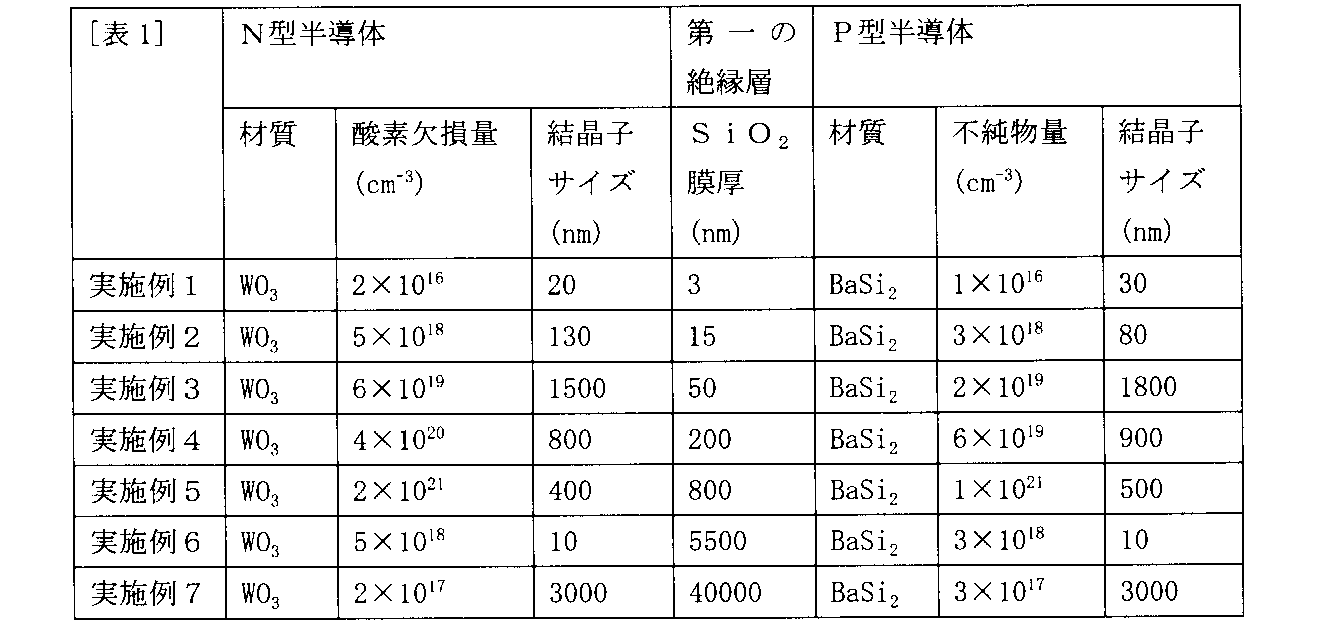
- Example 7 A P-type BaSi 2 layer was prepared as a P-type semiconductor.
- an N-type WO 3 layer was prepared as an N-type semiconductor.
- a SiO 2 layer was prepared as the first insulating layer.
- the P-BaSi 2 layers were prepared that varied impurity doping amount and the grain boundary volume.
- the thickness of the P-type BaSi 2 layer was unified to 0.5 ⁇ m (500 nm).
- the N-type WO 3 layer was prepared by changing the oxygen deficiency amount and the grain boundary amount.
- the thickness of the N-type WO 3 layer was unified to 0.5 ⁇ m (500 nm). This adjusted the introduction of the trap level.
- the first insulating layer was prepared by changing the film thickness by changing the sputtering conditions of SiO 2 .
- the film density of the SiO 2 film was unified to 95% and the relative dielectric constant was 3.8.
- the film density here is the film density relative to the true density. That is, in Examples 1 to 7, the film density of the first insulating layer was unified to 95% of the true density of SiO 2 .
- the areas of the semiconductor layer and insulating layer were all unified to 4 cm 2 .
- the position of the trap level when the band gap width (Ec ⁇ Ev) is 100, more specifically, the position when the bottom Ec of the conduction band is 100 and the vertex Ev of the valence band is 0 is , P-type semiconductor is unified to 1-3, N-type semiconductor is unified to 97-99.
- the level positions shown here are expressed as a range from the minimum value to the maximum value obtained when the same thing is measured three times by the method described above.
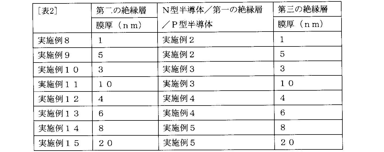
- Example 8 to 15 For the semiconductor solid state batteries according to Examples 2 to 5, the second insulating layer and the third insulating layer shown in Table 2 were provided. The second insulating layer and the third insulating layer were SiO 2 layers, and the film density was 95% and the relative dielectric constant was 3.8. Moreover, the electrode layer was unified with the Al layer.
- the battery was charged to a voltage of 2.0 V with a constant current using a charging / discharging device, and continuously discharged to 0 V with a constant current.
- the capacity (mAh) of the semiconductor solid battery was determined from the electric capacity at the time of discharge.
- the weight of the power storage unit represents the total weight of the semiconductor layer and the insulating layer excluding the substrate (the substrate used when forming the semiconductor layer) and the electrode layer.
- the semiconductor solid calculates the product of the capacity (mAh) and the average discharge voltage (V) of the battery was further determined energy density expressed by ⁇ Wh / cm 2 dividing it by the area 4 cm 2 of power storage unit.
- the area of the power storage unit represents an average area of the semiconductor layer and the insulating layer excluding the substrate and the electrode layer.
- the measurement of voltage drop was performed as follows. First, charging was performed by applying a constant voltage of 1.5 V to the battery for 50 seconds with a voltage source. Immediately after that, the connection with the voltage source was disconnected by switching on the circuit or the like, and instead, a constant load resistance of 0.9 M ⁇ was connected in series with the battery. The battery voltage was monitored with a voltmeter, and the voltage drop (V) immediately after the constant load resistance of 0.9 M ⁇ was measured.
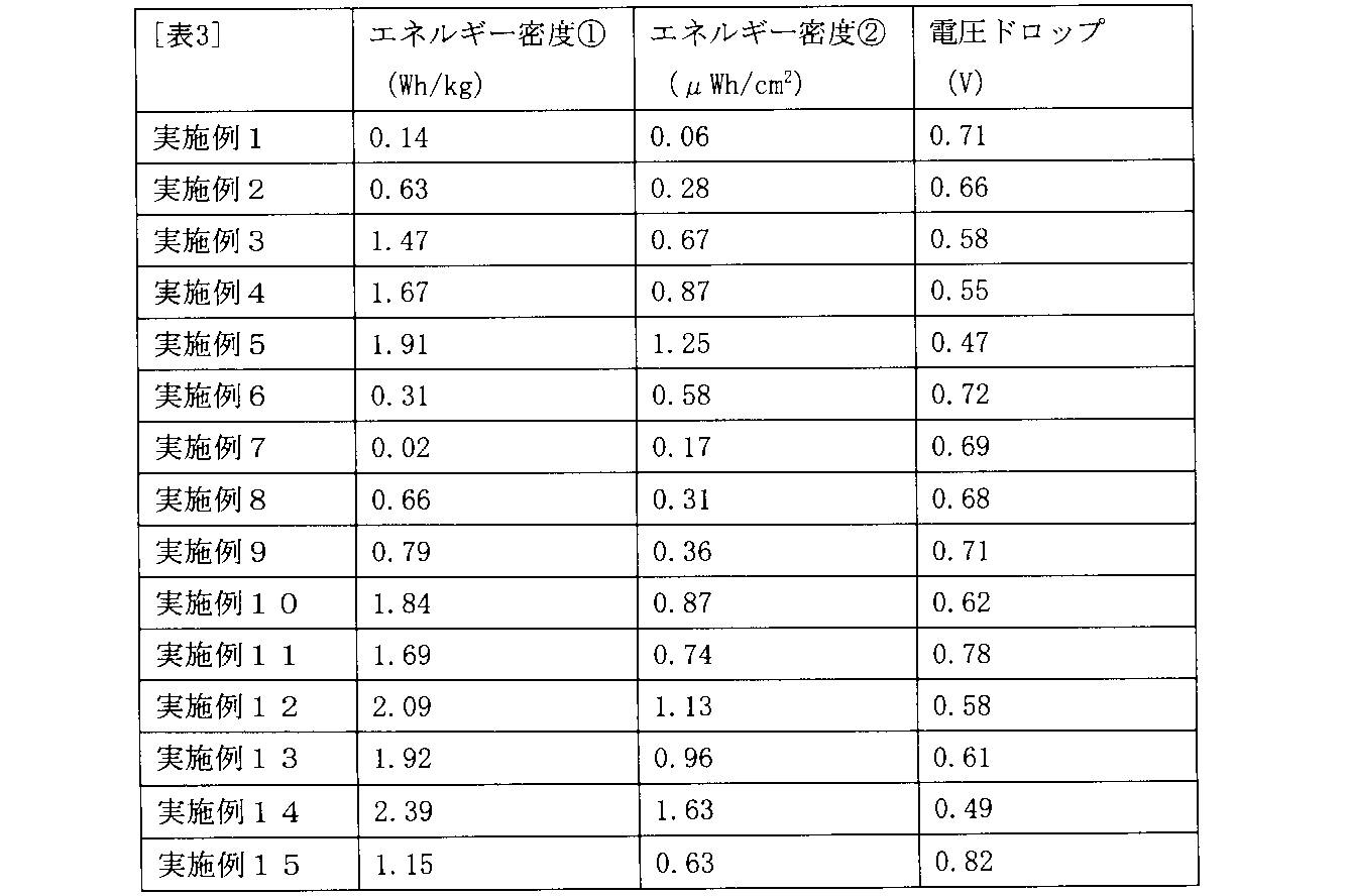
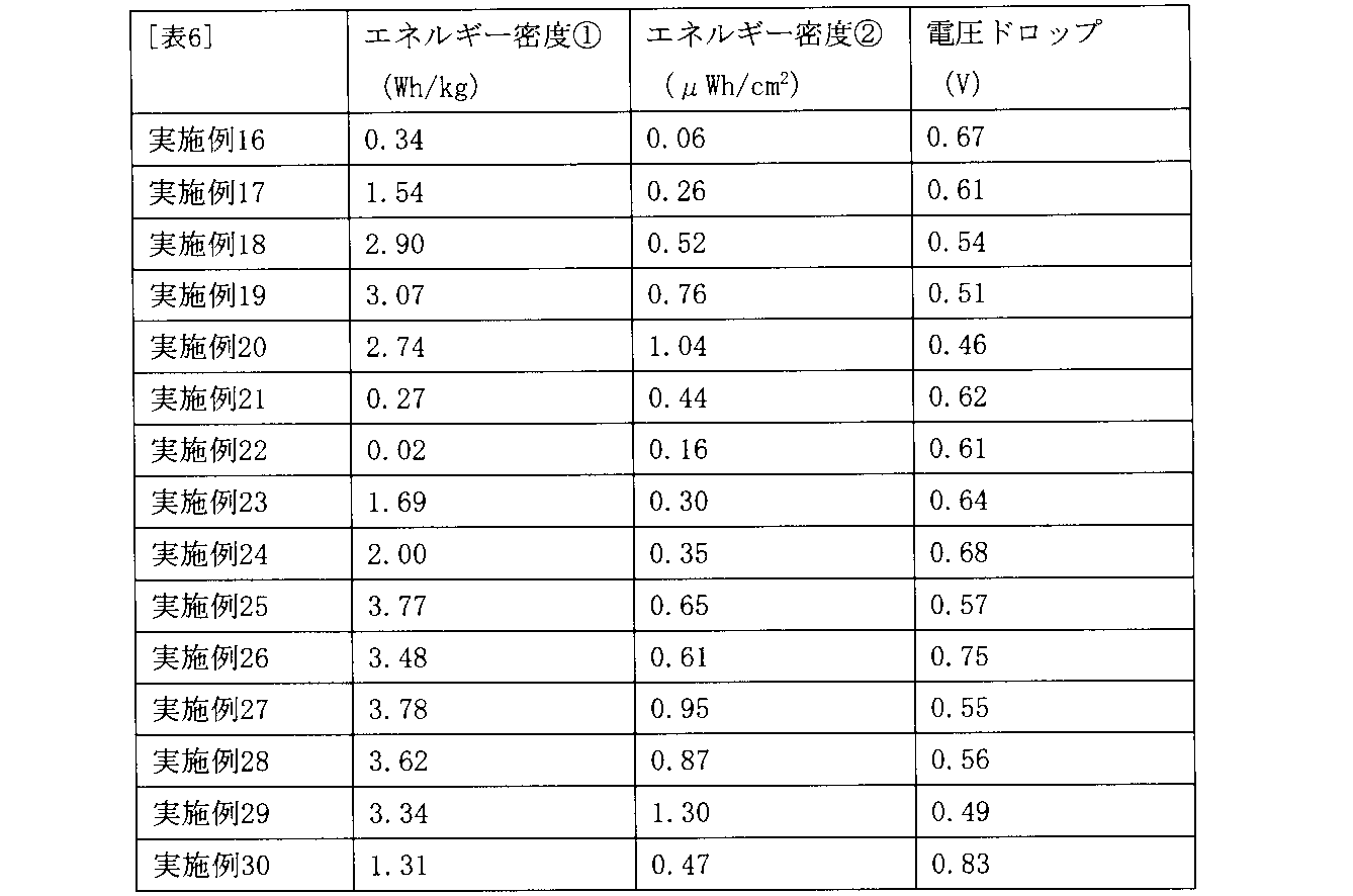
- the semiconductor solid battery according to the example has improved energy density and suppressed voltage drop. Further, by controlling the trap level and crystallite size, the energy density reached 1.91 Wh / kg, 1.25 ⁇ Wh / cm 2 , and the voltage drop could be 0.47V. Further, by providing the second insulating layer and the third insulating layer, the energy density reached 2.39 Wh / kg, 1.63 ⁇ Wh / cm 2 .
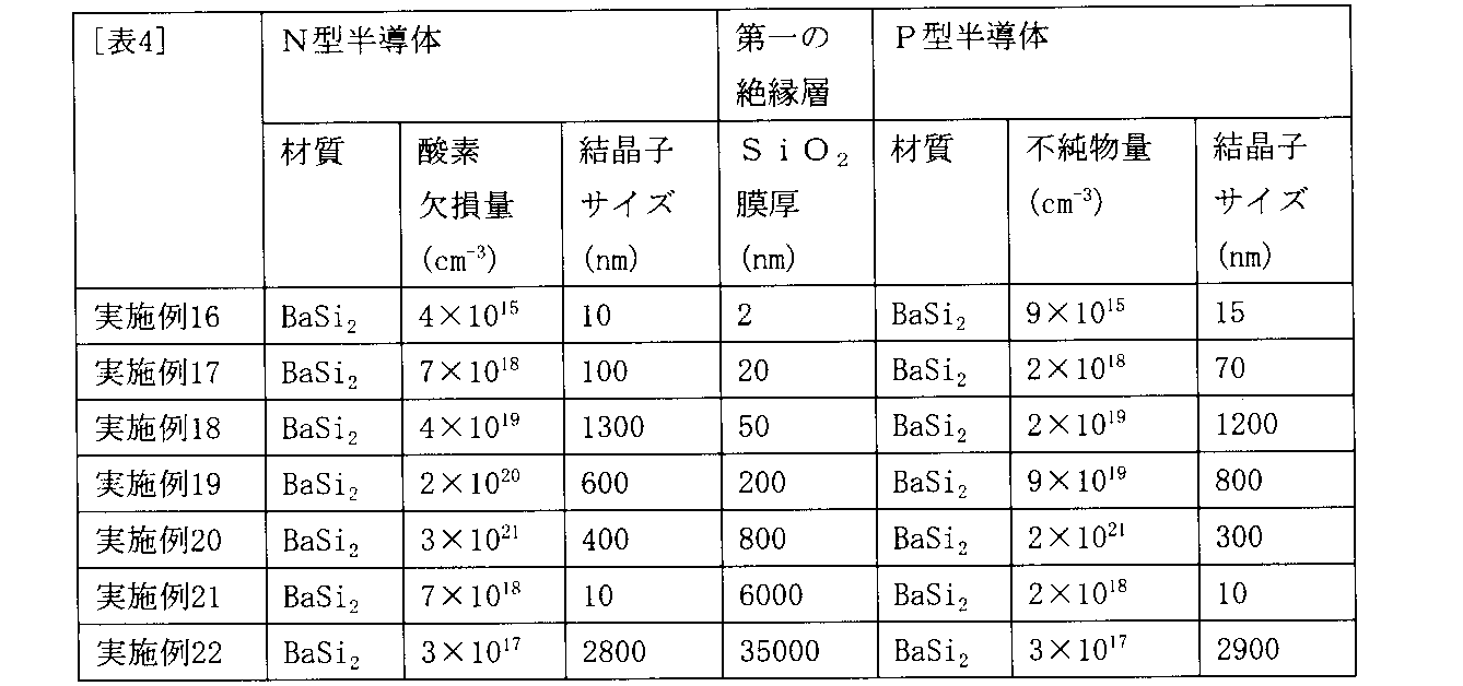
- a P-type BaSi 2 layer was prepared as a P-type semiconductor.
- an N-type BaSi 2 layer was prepared as an N-type semiconductor.
- a Si 3 N 4 layer was prepared as the first insulating layer.
- the P-type BaSi 2 layer and the N-type BaSi 2 layer were prepared by changing the impurity doping amount and the grain boundary amount.
- the thicknesses of the P-type BaSi 2 layer and the N-type BaSi 2 layer were unified to 0.5 ⁇ m (500 nm). This adjusted the introduction of the trap level.
- the first insulating layer was prepared by changing the film thickness by changing the sputtering conditions of Si 3 N 4 .
- the film density of the Si 3 N 4 film was unified to 93% and the relative dielectric constant was 7.5.
- the area of the insulating layer is unified all 4 cm 2.
- the level positions are unified to 1 to 3 for P-type semiconductors and 97 to 99 for N-type semiconductors.
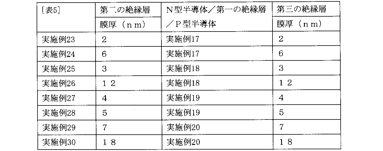
- Example 23 to Example 30 The semiconductor insulation batteries according to Examples 17 to 20 were provided with the second insulating layer and the third insulating layer shown in Table 5.
- the second insulating layer and the third insulating layer were Si 3 N 4 layers, and the film density was 93% and the relative dielectric constant was 7.5.
- the electrode layer was unified with the Al layer.
- the semiconductor solid battery according to the example has improved energy density and suppressed voltage drop. Further, by controlling the trap level and crystallite size, the energy density reached 3.07 Wh / kg and 1.04 ⁇ Wh / cm 2 , and the voltage drop could be reduced to 0.46 V or less. Further, by providing the second insulating layer and the third insulating layer, the energy density reached 3.78 Wh / kg, 1.30 ⁇ Wh / cm 2 .
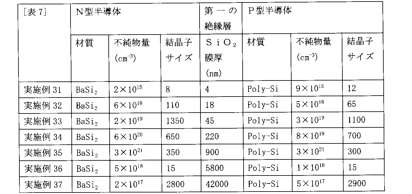
- Poly-Si polycrystalline silicon
- N-type BaSi 2 layer was prepared as an N-type semiconductor.
- SiO 2 layer was prepared as the first insulating layer.
- the P-type Poly-Si layer and the N-type BaSi 2 layer were prepared by changing the impurity doping amount and the grain boundary amount.
- the thicknesses of the P-type Poly-Si layer and the N-type BaSi 2 layer were unified to 0.5 ⁇ m (500 nm). This adjusted the introduction of the trap level.
- the first insulating layer was prepared by changing the film thickness by changing the sputtering conditions of SiO 2 .
- the film density of the SiO 2 film was unified to 95% and the relative dielectric constant was 3.8.
- the areas of the semiconductor layer and insulating layer were all unified to 4 cm 2 .
- the level positions are unified to 1 to 3 for P-type semiconductors and 97 to 99 for N-type semiconductors.
- Example 38 to Example 45 For the semiconductor solid state batteries according to Examples 32 to 35, the second insulating layer and the third insulating layer shown in Table 8 were provided. The second insulating layer and the third insulating layer were SiO 2 layers, and the film density was 95% and the relative dielectric constant was 3.8. Moreover, the electrode layer was unified with the Al layer.
- the semiconductor solid battery according to the example has improved energy density and suppressed voltage drop. Further, by controlling the trap level and crystallite size, the energy density reached 4.71 Wh / kg, 1.46 ⁇ Wh / cm 2 , and the voltage drop could be 0.50V. In addition, by providing the second insulating layer and the third insulating layer, the energy density reached 6.17 Wh / kg and 1.76 ⁇ Wh / cm 2 .
- the characteristics are improved by introducing the trap level.
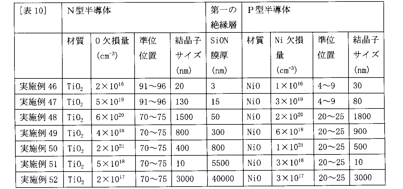
- Example 46 As a P-type semiconductor, a P-type NiO layer into which Ni deficiency was introduced was prepared. In addition, an N-type TiO 2 layer into which O deficiency was introduced was prepared as an N-type semiconductor. A SiON layer was prepared as the first insulating layer.
- a P-type NiO layer was prepared by changing the amount of Ni deficiency, the level position, and the amount of grain boundaries. As for the amount of Ni deficiency and the level position, a level due to Ni defects was provided by controlling the oxygen partial pressure during the formation of some P-type NiO layers. The thickness of the P-type NiO layer was unified to 0.5 ⁇ m (500 nm).
- the N-type TiO 2 layer was prepared by changing the amount of O deficiency, the level position, and the amount of grain boundary. As for the O deficiency and the level position, the level due to the O defect was provided by controlling the oxygen partial pressure during the formation of a part of the N-type TiO 2 layer. The thickness of the N-type TiO 2 layer was unified to 0.5 ⁇ m (500 nm).
- the first insulating layer was prepared by changing the film thickness by changing the sputtering conditions of SiON.
- the SiON film has a uniform film density of 90% and a relative dielectric constant of 7.3.
- the level position was within the range shown in Table 10.
- the level positions shown in Table 10 are expressed as a range from the minimum value to the maximum value obtained when the same thing is measured three times. Thereby, a semiconductor solid battery having the structure shown in Table 10 was produced.
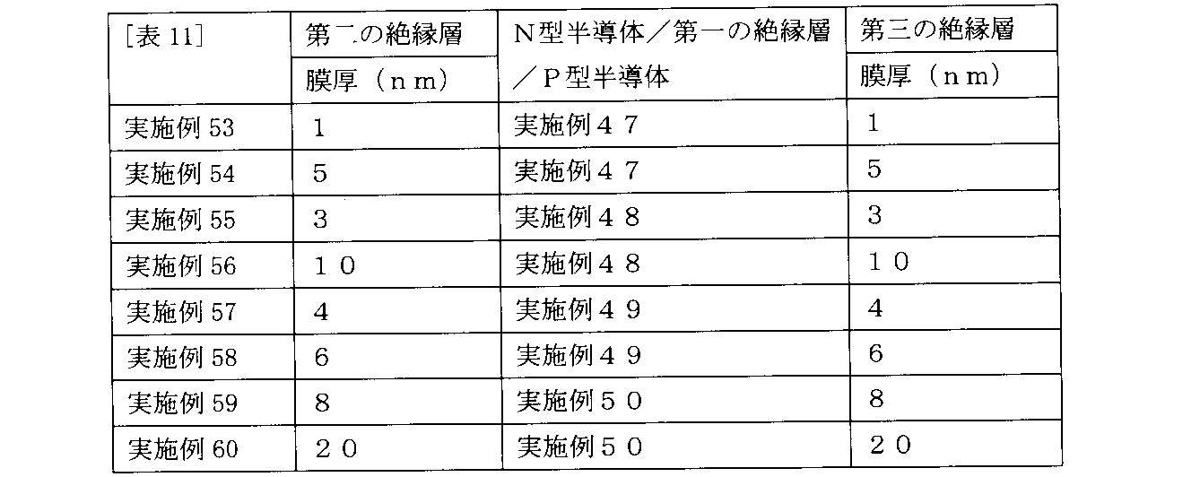
- Example 53 to 60 For the semiconductor solid state batteries according to Examples 46 to 52, the second insulating layer and the third insulating layer shown in Table 11 were provided.
- the second insulating layer and the third insulating layer were SiON layers, and the film density was 90% and the relative dielectric constant was 7.3.
- the electrode layer was unified with Au / Ti as the negative electrode on the TiO 2 layer side, and ITO as the positive electrode on the NiO layer side.
- Comparative Example 1 A semiconductor solid state battery was produced using a thin film in which a metal oxide semiconductor material and an insulating material were mixed as follows. A coating solution prepared by mixing and stirring fatty acid titanium and silicone oil in a solvent was spin-coated to form a charge layer (1 ⁇ m). Dried and heated 30 minutes at 350 ° C. After the give the TiO 2 and the silicone mixed film of. Furthermore, ultraviolet irradiation with a wavelength of 254 nm and an intensity of 20 mW / cm 2 was performed for about 40 minutes to introduce trap levels. A block layer NiO (150 nm) was formed on the charge layer. ITO was used for both positive and negative electrodes, and the area of the charge layer and block layer was 4 cm 2 . Thus, a semiconductor solid battery as Comparative Example 1 was produced.
- the semiconductor solid batteries according to Examples 47 to 51 and 53 to 60 have improved energy density and suppressed voltage drop as compared with Comparative Example 1. Further, by introducing the deep trap level, energy density 3.12Wh / kg or more, reach the 2.4 ⁇ Wh / cm 2, it was possible to suppress the voltage drop down to 0.35 V. Compared with Examples 1 to 45, the energy density of ⁇ Wh / kg obtained by unifying the area of the power storage unit at 4 cm 2 could be improved. Regarding the energy density in units of Wh / kg, the maximum performance value is inferior to that of Examples 1 to 45. This is considered to be due to the difference in film density due to the difference in the used semiconductor material and insulating layer material.
- FIG. 8 shows a discharge curve when the voltage drop in Example 49 was measured.
- the horizontal axis indicates time and the vertical axis indicates the battery voltage.
- the time when discharge was started that is, the time when the connection of the battery was switched from the connection with the voltage source (constant voltage of 1.5 V) to the connection with the constant load resistance (0.9 M ⁇ ) was set to zero.
- the battery voltage rapidly drops from 1.5 to 1.01 V at the start of discharge (time: 0 sec).
- the amount of voltage drop is represented as voltage drop D.
- Example 61 to 67 As a P-type semiconductor, a P-type ⁇ -FeSi 2 layer in which the composition ratio of Fe / Si was controlled was prepared. Further, an N-type TiO 2 layer was prepared as an N-type semiconductor. In addition, an HfO 2 layer was prepared as the first insulating layer.
- the N-type TiO 2 layer was prepared by changing the O deficiency amount, the level position, and the grain boundary amount. Part of the N-type TiO 2 layer was heat treated in a vacuum atmosphere to provide a level due to O defects. The thickness of the N-type TiO 2 layer was unified to 0.5 ⁇ m (500 nm).
- the first insulating layer was prepared by changing the film thickness by changing the sputtering conditions of HfO 2 .
- the film density of the HfO 2 film was unified to 95%, and the relative dielectric constant was unified to 25.0.
- the solid semiconductor batteries according to Examples 62 to 66 have improved energy density and suppressed voltage drop. Moreover, by introducing the trap level into a deep level, the energy density reached 2.09 Wh / kg and 2.04 ⁇ Wh / cm 2 , and the voltage drop could be suppressed to 0.33V.
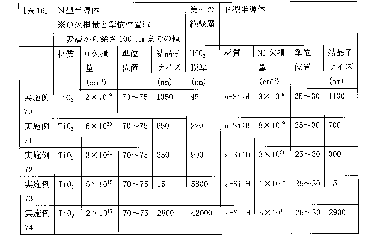
- Example 68 to 74 P-type a-Si: H was prepared as a P-type semiconductor. Further, an N-type TiO 2 layer was prepared as an N-type semiconductor. In addition, an HfO 2 layer was prepared as the first insulating layer.
- the P-type a-Si: H layer was formed by plasma CVD using diborane (B 2 H 6 ) gas, and a layer with different impurity doping amount, level position, and grain boundary amount was prepared.
- the thicknesses of the P-type a-Si: H layer and the N-type TiO 2 layer were unified to 0.5 ⁇ m (500 nm).
- N-type TiO 2 layer a level due to O defects was provided in the TiO 2 semiconductor as follows.
- oxygen vacancies were provided by annealing after film formation.
- Examples 70-74 by laser treatment of the surface of the N-type TiO 2 layer, provided levels by O defect only in the vicinity of the surface layer.
- the first insulating layer was prepared by changing the film thickness by changing the sputtering conditions of SiO 2 .
- the film density of the HfO 2 film was unified to 95% and the relative dielectric constant was 25.
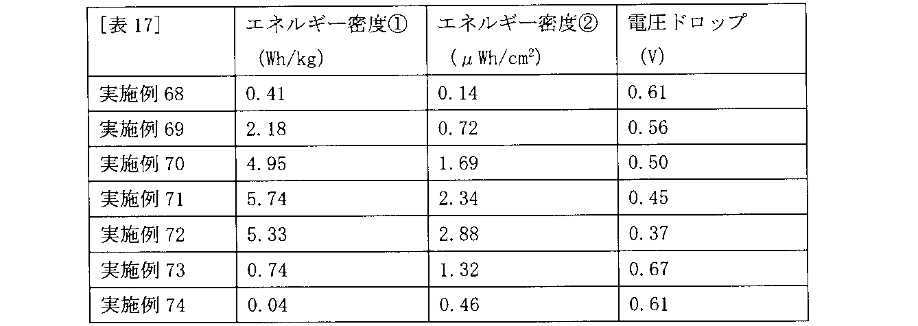
- the semiconductor solid batteries according to Examples 69 to 73 have improved energy density and suppressed voltage drop. Further, by introducing the trap level into a deep level, the energy density reached 5.74 Wh / kg, 2.88 ⁇ Wh / cm 2 , and the voltage drop could be suppressed to 0.37V.
- Example 75 A semiconductor solid state battery in which the N-type semiconductor layer of Example 4 was replaced with the N-type semiconductor layer of Example 49 was produced as Example 75. Further, a semiconductor solid battery in which the P-type semiconductor layer of Example 4 was replaced with the P-type semiconductor layer of Example 49 was produced as Example 76.
- the semiconductor solid batteries according to Examples 75 and 76 have improved energy density and suppressed voltage drop.
- the energy density improvement and the voltage drop suppression could also be confirmed by deepening the trap level position of only one of the N-type semiconductor layer and the P-type semiconductor layer.
- the characteristics were improved by controlling the first insulating layer, the second insulating layer, and the third insulating layer. Even if the materials of the N-type semiconductor and the P-type semiconductor are changed, the characteristics are improved by introducing the trap level.
- an N-type semiconductor, a P-type semiconductor, and a first insulating layer are included, and the first insulating layer is provided between the N-type semiconductor and the P-type semiconductor.
- a solid state semiconductor battery is provided. This semiconductor solid battery has a high energy density and a small voltage drop.
Landscapes
- Chemical & Material Sciences (AREA)
- Chemical Kinetics & Catalysis (AREA)
- Electrochemistry (AREA)
- General Chemical & Material Sciences (AREA)
- Engineering & Computer Science (AREA)
- Manufacturing & Machinery (AREA)
- Inorganic Chemistry (AREA)
- Physics & Mathematics (AREA)
- Condensed Matter Physics & Semiconductors (AREA)
- General Physics & Mathematics (AREA)
- Battery Electrode And Active Subsutance (AREA)
- Secondary Cells (AREA)
Abstract
Description
SiO2の場合3.0~5.0、Al2O3の場合7.0~10.0、SiONの場合5.0~9.0、Si3N4の場合6.5~9.0、AlNの場合7.5~10.5、HfO2の場合22.0~26.0、シリコーン樹脂の場合2.0~4.0。

Nd :伝導帯のキャリア密度、No :最近接ホッピング伝導帯のキャリア密度
μb :伝導帯のキャリア移動度、 μh :最近接ホッピング伝導帯のキャリア移動度
Ea :準位と伝導帯下端のエネルギー差、q:電気素量、
ε :準位での近接キャリアトラップ間の電子の平均活性化エネルギー。
(実施例1~7)
P型半導体として、P型BaSi2層を用意した。また、N型半導体としてN型WO3層を用意した。また、第一の絶縁層としてSiO2層を用意した。
実施例2~実施例5にかかる半導体固体電池に対し、表2に示す第二の絶縁層および第三の絶縁層を設けた。第二の絶縁層および第三の絶縁層は、SiO2層とし、膜密度95%、比誘電率3.8に統一した。また、電極層はAl層で統一した。
P型半導体として、P型BaSi2層を用意した。また、N型半導体としてN型BaSi2層を用意した。また、第一の絶縁層としてSi3N4層を用意した。
実施例17~実施例20にかかる半導体固体電池に対し、表5に示す第二の絶縁層および第三の絶縁層を設けた。第二の絶縁層および第三の絶縁層は、Si3N4層とし、膜密度93%、比誘電率7.5に統一した。また、電極層はAl層で統一した。
P型半導体として、Poly-Si(多結晶シリコン)を用意した。また、N型半導体としてN型BaSi2層を用意した。また、第一の絶縁層としてSiO2層を用意した。
実施例32~実施例35にかかる半導体固体電池に対し、表8に示す第二の絶縁層および第三の絶縁層を設けた。第二の絶縁層および第三の絶縁層は、SiO2層とし、膜密度95%、比誘電率3.8に統一した。また、電極層はAl層で統一した。


P型半導体として、Ni欠損を導入したP型NiO層を用意した。また、N型半導体としてO欠損を導入したN型TiO2層を用意した。また、第一の絶縁層としてSiON層を用意した。
実施例46~実施例52にかかる半導体固体電池に対し、表11に示す第二の絶縁層および第三の絶縁層を設けた。第二の絶縁層および第三の絶縁層は、SiON層とし、膜密度90%、比誘電率7.3に統一した。また、電極層はTiO2層側の負電極としてAu/Ti、NiO層側の正電極としてITOで統一した。
次のようにして、金属酸化物半導体材料と絶縁材料を混合した薄膜を用いて、半導体固体電池を作製した。脂肪酸チタンとシリコーンオイルを溶媒に混合して撹拌し作製した塗布液をスピンコートし、充電層(1μm)を形成した。乾燥した後に350℃で30分加熱し、TiO2とシリコーンの混合膜を得た。さらに、波長254nm、強度20mW/cm2の紫外線照射を約40分間行い、捕獲準位を導入した。充電層の上部にブロック層NiO(150nm)を成膜した。正負電極共にITOを使用し、充電層やブロック層の面積は4cm2とした。こうして、比較例1としての半導体固体電池を作製した。

P型半導体として、Fe/Siの組成比を制御したP型β-FeSi2層を用意した。また、N型半導体としてN型TiO2層を用意した。また、第一の絶縁層としてHfO2層を用意した。


P型半導体として、P型a-Si:Hを用意した。また、N型半導体としてN型TiO2層を用意した。また、第一の絶縁層としてHfO2層を用意した。

実施例4のN型半導体層を実施例49のN型半導体層に置き換えた半導体固体電池を実施例75として作製した。また、実施例4のP型半導体層を実施例49のP型半導体層に置き換えた半導体固体電池を実施例76として作製した。

Claims (12)
- N型半導体とP型半導体との間に第一の絶縁層を設けた半導体固体電池。
- 前記第一の絶縁層は膜厚が3nm以上30μm以下、かつ比誘電率が50以下である請求項1記載の半導体固体電池。
- 前記第一の絶縁層の比誘電率が10以下である請求項2に記載の半導体固体電池。
- 前記第一の絶縁層は膜密度が真密度の60%以上である請求項1ないし請求項3のいずれか1項に記載の半導体固体電池。
- 前記N型半導体および前記P型半導体の少なくとも一方は、金属シリサイド、金属酸化物、アモルファスシリコン、結晶シリコン、多結晶シリコン、単結晶シリコンからなる群より選ばれる1種からなる請求項1ないし請求項4のいずれか1項に記載の半導体固体電池。
- 前記N型半導体または前記P型半導体は、電子または正孔の捕獲準位を導入している請求項1ないし請求項5のいずれか1項に記載の半導体固体電池。
- 前記N型半導体は、前記N型半導体におけるバンドギャップを100としたとき、50以上90以下の範囲に前記電子の捕獲準位が導入されている請求項6に記載の半導体固体電池。
- 前記P型半導体は、前記P型半導体におけるバンドギャップを100としたとき、10以上50以下の範囲に前記正孔の捕獲準位が導入されている請求項6又は7に記載の半導体固体電池。
- 前記N型半導体および前記P型半導体にそれぞれ電極が設けられている請求項1ないし請求項8のいずれか1項に記載の半導体固体電池。
- 前記N型半導体と前記電極との間に第二の絶縁層が設けられている、または前記P型半導体と前記電極との間に第三の絶縁層が設けられている、または前記N型半導体と前記電極との間に前記第二の絶縁層が設けられていると共に前記P型半導体と前記電極との間に前記第三の絶縁層とのが設けられている請求項9記載の半導体固体電池。
- 前記第二の絶縁層および前記第三の絶縁層の少なくとも一方は膜厚が30nm以下、かつ比誘電率が50以下である請求項10に記載の半導体固体電池。
- 前記第二の絶縁層および前記第三の絶縁層の少なくとも一方の比誘電率が10以下である請求項11に記載の半導体固体電池。
Priority Applications (4)
| Application Number | Priority Date | Filing Date | Title |
|---|---|---|---|
| CN201780073814.XA CN110024154B (zh) | 2016-12-21 | 2017-12-21 | 半导体固体电池 |
| KR1020197015196A KR102282074B1 (ko) | 2016-12-21 | 2017-12-21 | 반도체 고체 전지 |
| JP2018558077A JP7010843B2 (ja) | 2016-12-21 | 2017-12-21 | 半導体固体電池 |
| US16/437,459 US11600866B2 (en) | 2016-12-21 | 2019-06-11 | Semiconductor solid state battery |
Applications Claiming Priority (2)
| Application Number | Priority Date | Filing Date | Title |
|---|---|---|---|
| JP2016-247739 | 2016-12-21 | ||
| JP2016247739 | 2016-12-21 |
Related Child Applications (1)
| Application Number | Title | Priority Date | Filing Date |
|---|---|---|---|
| US16/437,459 Continuation US11600866B2 (en) | 2016-12-21 | 2019-06-11 | Semiconductor solid state battery |
Publications (1)
| Publication Number | Publication Date |
|---|---|
| WO2018117235A1 true WO2018117235A1 (ja) | 2018-06-28 |
Family
ID=62626756
Family Applications (1)
| Application Number | Title | Priority Date | Filing Date |
|---|---|---|---|
| PCT/JP2017/046002 Ceased WO2018117235A1 (ja) | 2016-12-21 | 2017-12-21 | 半導体固体電池 |
Country Status (5)
| Country | Link |
|---|---|
| US (1) | US11600866B2 (ja) |
| JP (1) | JP7010843B2 (ja) |
| KR (1) | KR102282074B1 (ja) |
| CN (1) | CN110024154B (ja) |
| WO (1) | WO2018117235A1 (ja) |
Cited By (3)
| Publication number | Priority date | Publication date | Assignee | Title |
|---|---|---|---|---|
| JP2021097151A (ja) * | 2019-12-18 | 2021-06-24 | 株式会社東芝 | 半導体固体電池 |
| JP2021181390A (ja) * | 2020-05-19 | 2021-11-25 | 国立大学法人 筑波大学 | 半導体固体電池および半導体固体電池の準位判断方法 |
| WO2026075046A1 (ja) * | 2024-10-02 | 2026-04-09 | 株式会社ディメンジョンフォー | 物理二次電池 |
Families Citing this family (1)
| Publication number | Priority date | Publication date | Assignee | Title |
|---|---|---|---|---|
| JP7244386B2 (ja) * | 2019-07-30 | 2023-03-22 | 株式会社Uacj | 半導体電池、負極材、正極材及び半導体電池の製造方法 |
Citations (3)
| Publication number | Priority date | Publication date | Assignee | Title |
|---|---|---|---|---|
| WO2012046325A1 (ja) * | 2010-10-07 | 2012-04-12 | グエラテクノロジー株式会社 | 二次電池 |
| JP2015195335A (ja) * | 2014-03-24 | 2015-11-05 | パナソニックIpマネジメント株式会社 | 蓄電素子及び蓄電素子の製造方法 |
| JP2016014128A (ja) * | 2014-06-09 | 2016-01-28 | 出光興産株式会社 | 二次電池及びそれに用いる構造体 |
Family Cites Families (8)
| Publication number | Priority date | Publication date | Assignee | Title |
|---|---|---|---|---|
| JP2001338649A (ja) | 2000-05-29 | 2001-12-07 | Toshiba Corp | 非水電解液二次電池用正極材料およびそれを用いた非水電解液二次電池 |
| JP4563503B2 (ja) * | 2007-12-26 | 2010-10-13 | パナソニック株式会社 | 非水電解質二次電池 |
| EP2858102B1 (en) | 2012-05-31 | 2020-04-22 | Kabushiki Kaisha Nihon Micronics | Semiconductor probe for testing quantum cell, test device, and test method |
| WO2013183132A1 (ja) * | 2012-06-06 | 2013-12-12 | 株式会社日本マイクロニクス | 固体型二次電池の電極構造 |
| JP2014154223A (ja) | 2013-02-05 | 2014-08-25 | Ricoh Co Ltd | 二次電池モジュールおよび太陽電池−二次電池一体型給電素子 |
| JP2016028408A (ja) * | 2014-03-24 | 2016-02-25 | パナソニックIpマネジメント株式会社 | 蓄電素子及び蓄電素子の製造方法 |
| JP2017182969A (ja) | 2016-03-29 | 2017-10-05 | イムラ・ジャパン株式会社 | 二次電池及びその製造方法 |
| JP6854100B2 (ja) * | 2016-08-31 | 2021-04-07 | 株式会社日本マイクロニクス | 二次電池 |
-
2017
- 2017-12-21 KR KR1020197015196A patent/KR102282074B1/ko active Active
- 2017-12-21 CN CN201780073814.XA patent/CN110024154B/zh active Active
- 2017-12-21 JP JP2018558077A patent/JP7010843B2/ja active Active
- 2017-12-21 WO PCT/JP2017/046002 patent/WO2018117235A1/ja not_active Ceased
-
2019
- 2019-06-11 US US16/437,459 patent/US11600866B2/en active Active
Patent Citations (3)
| Publication number | Priority date | Publication date | Assignee | Title |
|---|---|---|---|---|
| WO2012046325A1 (ja) * | 2010-10-07 | 2012-04-12 | グエラテクノロジー株式会社 | 二次電池 |
| JP2015195335A (ja) * | 2014-03-24 | 2015-11-05 | パナソニックIpマネジメント株式会社 | 蓄電素子及び蓄電素子の製造方法 |
| JP2016014128A (ja) * | 2014-06-09 | 2016-01-28 | 出光興産株式会社 | 二次電池及びそれに用いる構造体 |
Cited By (5)
| Publication number | Priority date | Publication date | Assignee | Title |
|---|---|---|---|---|
| JP2021097151A (ja) * | 2019-12-18 | 2021-06-24 | 株式会社東芝 | 半導体固体電池 |
| JP7346275B2 (ja) | 2019-12-18 | 2023-09-19 | 株式会社東芝 | 半導体固体電池 |
| JP2021181390A (ja) * | 2020-05-19 | 2021-11-25 | 国立大学法人 筑波大学 | 半導体固体電池および半導体固体電池の準位判断方法 |
| JP7698259B2 (ja) | 2020-05-19 | 2025-06-25 | 国立大学法人 筑波大学 | 半導体固体電池および半導体固体電池の準位判断方法 |
| WO2026075046A1 (ja) * | 2024-10-02 | 2026-04-09 | 株式会社ディメンジョンフォー | 物理二次電池 |
Also Published As
| Publication number | Publication date |
|---|---|
| JPWO2018117235A1 (ja) | 2019-10-31 |
| KR20190076013A (ko) | 2019-07-01 |
| US11600866B2 (en) | 2023-03-07 |
| JP7010843B2 (ja) | 2022-01-26 |
| CN110024154A (zh) | 2019-07-16 |
| KR102282074B1 (ko) | 2021-07-27 |
| US20190296401A1 (en) | 2019-09-26 |
| CN110024154B (zh) | 2023-06-20 |
Similar Documents
| Publication | Publication Date | Title |
|---|---|---|
| US10283776B2 (en) | Electrode material, and electrode layer, battery, and electrochromic device using the electrode material | |
| US11600866B2 (en) | Semiconductor solid state battery | |
| Tao et al. | Co-electrodeposited Cu 2 ZnSnS 4 thin-film solar cells with over 7% efficiency fabricated via fine-tuning of the Zn content in absorber layers | |
| US10686087B2 (en) | Solar cell and method for manufacturing the same | |
| KR101613846B1 (ko) | 태양 전지 및 이의 제조 방법 | |
| TWI452714B (zh) | 太陽能電池及其製造方法 | |
| JP6438249B2 (ja) | 電極材料およびそれを用いた電極層、電池並びにエレクトロクロミック素子 | |
| JP6977929B2 (ja) | 半導体固体電池 | |
| Zhang et al. | Improving the photovoltaic performance of solid-state ZnO/CdTe core–shell nanorod array solar cells using a thin CdS interfacial layer | |
| JP5826094B2 (ja) | p型半導体材料、および光電変換装置の作製方法 | |
| CN104364910B (zh) | 制造磷属元素化物吸收体膜和发射体膜之间导带偏移降低的光伏器件的方法 | |
| JP2018101560A (ja) | 半導体固体電池 | |
| JP7346275B2 (ja) | 半導体固体電池 | |
| Liu et al. | Solution-processed tungsten oxide with Ta 5+ doping enhances the hole selective transport for crystalline silicon solar cells | |
| JP5980060B2 (ja) | 太陽電池 | |
| JP2018505311A (ja) | カルコゲナイド半導体を製作するために有用なアルカリ金属含有前駆体膜の高速スパッタ堆積 | |
| Xu et al. | Fabrication of Cu2Zn (Sn, Si) S4 thin films using a two-step method for solar cell applications | |
| WO2012153640A1 (ja) | 光電変換素子および太陽電池 | |
| JP5980059B2 (ja) | 太陽電池 | |
| KR101922065B1 (ko) | 박막 태양전지의 제조방법 | |
| Khan et al. | In-situ antimony doping of CdTe | |
| JP5710369B2 (ja) | 光電変換素子および太陽電池 | |
| US20170236958A1 (en) | Photoelectric conversion device and photoelectric conversion module | |
| JP2014107558A (ja) | 太陽電池、及び太陽電池の製造方法 | |
| Heitmann et al. | Nanocrystalline Materials: Optimization of Thin Film Properties |
Legal Events
| Date | Code | Title | Description |
|---|---|---|---|
| 121 | Ep: the epo has been informed by wipo that ep was designated in this application |
Ref document number: 17883917 Country of ref document: EP Kind code of ref document: A1 |
|
| ENP | Entry into the national phase |
Ref document number: 2018558077 Country of ref document: JP Kind code of ref document: A |
|
| ENP | Entry into the national phase |
Ref document number: 20197015196 Country of ref document: KR Kind code of ref document: A |
|
| NENP | Non-entry into the national phase |
Ref country code: DE |
|
| 122 | Ep: pct application non-entry in european phase |
Ref document number: 17883917 Country of ref document: EP Kind code of ref document: A1 |