WO2018116937A1 - 情報処理装置およびメモリアクセス方法 - Google Patents
情報処理装置およびメモリアクセス方法 Download PDFInfo
- Publication number
- WO2018116937A1 WO2018116937A1 PCT/JP2017/044777 JP2017044777W WO2018116937A1 WO 2018116937 A1 WO2018116937 A1 WO 2018116937A1 JP 2017044777 W JP2017044777 W JP 2017044777W WO 2018116937 A1 WO2018116937 A1 WO 2018116937A1
- Authority
- WO
- WIPO (PCT)
- Prior art keywords
- queue
- command
- request
- information processing
- processing
- Prior art date
Links
Images


Classifications
-
- G—PHYSICS
- G06—COMPUTING; CALCULATING OR COUNTING
- G06F—ELECTRIC DIGITAL DATA PROCESSING
- G06F12/00—Accessing, addressing or allocating within memory systems or architectures
- G06F12/02—Addressing or allocation; Relocation
- G06F12/0223—User address space allocation, e.g. contiguous or non contiguous base addressing
- G06F12/023—Free address space management
- G06F12/0238—Memory management in non-volatile memory, e.g. resistive RAM or ferroelectric memory
- G06F12/0246—Memory management in non-volatile memory, e.g. resistive RAM or ferroelectric memory in block erasable memory, e.g. flash memory
-
- G—PHYSICS
- G06—COMPUTING; CALCULATING OR COUNTING
- G06F—ELECTRIC DIGITAL DATA PROCESSING
- G06F12/00—Accessing, addressing or allocating within memory systems or architectures
-
- G—PHYSICS
- G06—COMPUTING; CALCULATING OR COUNTING
- G06F—ELECTRIC DIGITAL DATA PROCESSING
- G06F12/00—Accessing, addressing or allocating within memory systems or architectures
- G06F12/02—Addressing or allocation; Relocation
-
- G—PHYSICS
- G06—COMPUTING; CALCULATING OR COUNTING
- G06F—ELECTRIC DIGITAL DATA PROCESSING
- G06F13/00—Interconnection of, or transfer of information or other signals between, memories, input/output devices or central processing units
- G06F13/14—Handling requests for interconnection or transfer
- G06F13/16—Handling requests for interconnection or transfer for access to memory bus
- G06F13/1605—Handling requests for interconnection or transfer for access to memory bus based on arbitration
- G06F13/1642—Handling requests for interconnection or transfer for access to memory bus based on arbitration with request queuing
-
- G—PHYSICS
- G06—COMPUTING; CALCULATING OR COUNTING
- G06F—ELECTRIC DIGITAL DATA PROCESSING
- G06F3/00—Input arrangements for transferring data to be processed into a form capable of being handled by the computer; Output arrangements for transferring data from processing unit to output unit, e.g. interface arrangements
- G06F3/06—Digital input from, or digital output to, record carriers, e.g. RAID, emulated record carriers or networked record carriers
- G06F3/0601—Interfaces specially adapted for storage systems
- G06F3/0602—Interfaces specially adapted for storage systems specifically adapted to achieve a particular effect
- G06F3/061—Improving I/O performance
- G06F3/0611—Improving I/O performance in relation to response time
-
- G—PHYSICS
- G06—COMPUTING; CALCULATING OR COUNTING
- G06F—ELECTRIC DIGITAL DATA PROCESSING
- G06F3/00—Input arrangements for transferring data to be processed into a form capable of being handled by the computer; Output arrangements for transferring data from processing unit to output unit, e.g. interface arrangements
- G06F3/06—Digital input from, or digital output to, record carriers, e.g. RAID, emulated record carriers or networked record carriers
- G06F3/0601—Interfaces specially adapted for storage systems
- G06F3/0628—Interfaces specially adapted for storage systems making use of a particular technique
- G06F3/0638—Organizing or formatting or addressing of data
- G06F3/064—Management of blocks
-
- G—PHYSICS
- G06—COMPUTING; CALCULATING OR COUNTING
- G06F—ELECTRIC DIGITAL DATA PROCESSING
- G06F3/00—Input arrangements for transferring data to be processed into a form capable of being handled by the computer; Output arrangements for transferring data from processing unit to output unit, e.g. interface arrangements
- G06F3/06—Digital input from, or digital output to, record carriers, e.g. RAID, emulated record carriers or networked record carriers
- G06F3/0601—Interfaces specially adapted for storage systems
- G06F3/0628—Interfaces specially adapted for storage systems making use of a particular technique
- G06F3/0646—Horizontal data movement in storage systems, i.e. moving data in between storage devices or systems
- G06F3/0647—Migration mechanisms
- G06F3/0649—Lifecycle management
-
- G—PHYSICS
- G06—COMPUTING; CALCULATING OR COUNTING
- G06F—ELECTRIC DIGITAL DATA PROCESSING
- G06F3/00—Input arrangements for transferring data to be processed into a form capable of being handled by the computer; Output arrangements for transferring data from processing unit to output unit, e.g. interface arrangements
- G06F3/06—Digital input from, or digital output to, record carriers, e.g. RAID, emulated record carriers or networked record carriers
- G06F3/0601—Interfaces specially adapted for storage systems
- G06F3/0628—Interfaces specially adapted for storage systems making use of a particular technique
- G06F3/0655—Vertical data movement, i.e. input-output transfer; data movement between one or more hosts and one or more storage devices
- G06F3/0658—Controller construction arrangements
-
- G—PHYSICS
- G06—COMPUTING; CALCULATING OR COUNTING
- G06F—ELECTRIC DIGITAL DATA PROCESSING
- G06F3/00—Input arrangements for transferring data to be processed into a form capable of being handled by the computer; Output arrangements for transferring data from processing unit to output unit, e.g. interface arrangements
- G06F3/06—Digital input from, or digital output to, record carriers, e.g. RAID, emulated record carriers or networked record carriers
- G06F3/0601—Interfaces specially adapted for storage systems
- G06F3/0628—Interfaces specially adapted for storage systems making use of a particular technique
- G06F3/0655—Vertical data movement, i.e. input-output transfer; data movement between one or more hosts and one or more storage devices
- G06F3/0659—Command handling arrangements, e.g. command buffers, queues, command scheduling
-
- G—PHYSICS
- G06—COMPUTING; CALCULATING OR COUNTING
- G06F—ELECTRIC DIGITAL DATA PROCESSING
- G06F3/00—Input arrangements for transferring data to be processed into a form capable of being handled by the computer; Output arrangements for transferring data from processing unit to output unit, e.g. interface arrangements
- G06F3/06—Digital input from, or digital output to, record carriers, e.g. RAID, emulated record carriers or networked record carriers
- G06F3/0601—Interfaces specially adapted for storage systems
- G06F3/0668—Interfaces specially adapted for storage systems adopting a particular infrastructure
- G06F3/0671—In-line storage system
- G06F3/0673—Single storage device
- G06F3/0679—Non-volatile semiconductor memory device, e.g. flash memory, one time programmable memory [OTP]
Definitions
- the present invention relates to an information processing apparatus and a memory access method for accessing a flash memory.
- management processing include the following. In other words, since NAND flash memory cannot be overwritten, if data is written in various areas as described above, copy them to a continuous area at any stage, Need to be erased in preparation for writing.
- the present invention has been made in view of these problems, and an object of the present invention is to provide a technique capable of stably performing information processing using an SSD while suppressing a delay time for memory access.
- An aspect of the present invention relates to an information processing apparatus.
- the information processing apparatus includes a command receiving unit that receives an access request to the memory from the host processor, and a command processing unit that reads and executes the access request from any of a plurality of queues in which the access requests are classified and stored. And a command processing unit that switches a request reading destination queue to a next among a plurality of queues at a timing according to a rule set for each queue.
- Still another aspect of the present invention relates to a memory access method.
- the memory controller receives a memory processor access request from the host processor, reads the access request from one of a plurality of queues that classify and store the access request, and reads the read access request.
- the step of reading out includes switching the request reading destination queue among the plurality of queues at a timing according to a rule set for each queue.
- 4 is a flowchart illustrating a processing procedure in which a command processing unit according to the present embodiment reads or writes data in phase 2;
- 6 is a flowchart illustrating a processing procedure in which a command processing unit according to the present embodiment performs a reading process in a management process in phase 3;
- 10 is a flowchart illustrating a processing procedure in which a command processing unit according to the present embodiment performs writing processing and data erasing among management processing in phase 5; It is a figure for demonstrating the form which introduces the rule which switches a phase according to the notification from a host unit in this Embodiment. It is a flowchart which shows the process sequence of the flash controller which focused on the adjustment by the command adjustment part of this Embodiment.
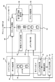
- FIG. 1 shows a circuit configuration of the information processing apparatus according to the present embodiment.
- the information processing apparatus exemplified here may be any of general information equipment such as a portable game machine, a personal computer, a mobile phone, a tablet terminal, and a PDA.
- the information processing apparatus 10 includes a host unit 12 including a CPU, a system memory 14, a NAND flash memory 20 (hereinafter simply referred to as a flash memory 20), and a flash controller 18.
- the host unit 12 loads programs and data stored in the flash memory 20 into the system memory 14 and performs information processing using the programs and data. Further, the application program and data are read from a recording medium driven by a recording medium driving unit (not shown) or downloaded from a server connected to the network by a communication unit and stored in the flash memory 20. At this time, the host unit 12 issues an access request to the flash memory 20 to the flash controller 18, and the flash controller 18 performs read / write processing on the flash memory 20 accordingly.
- a plurality of NAND flash memories are connected to the flash memory 20, and data is distributed and stored in a plurality of channels (four channels “ch0" to "ch3" in the figure) as shown.
- the flash controller 18 includes a host controller 22 having an interface function with the host unit 12, a memory controller 28 having an interface function with the flash memory 20, and an SRAM (Static Random Access Memory) 24.
- the host unit 12 generates an access request to the flash memory 20 according to the progress of information processing, and stores it in the system memory 14.
- the access request includes a logical address (LBA: Logical : Block Address) of the access destination.
- the host controller 22 of the flash controller 18 reads the access request stored in the system memory 14 and converts the LBA into a physical address of the flash memory 20. At this time, at least a part of the necessary address conversion table originally stored in the flash memory 20 is developed in the SRAM 24.
- reading and writing of data with respect to the flash memory 20 are performed in units of access such as 4096 bytes.
- data cannot be overwritten. Therefore, when writing data, it is necessary to secure an area where nothing is written. As described above, if only the logical address is changed in order to distribute the write area and data update is repeated, the area that stores the invalid original data will increase, and the area that can be newly written will eventually be exhausted. .
- the memory controller 28 recharges the leaked charges by saving the data of the entire block to another block.
- the command adjustment unit 50 adjusts the ratio of processing to be performed so that the management processing is not completed and the memory access does not fail. For example, when the number of commands for management processing stored in the queue 44 exceeds a predetermined threshold, at least one of the queue switching rules stored in the switching rule storage unit 48 is temporarily changed. Or notifies the host unit 12 to that effect.
- the command issuing unit 30 of the host unit 12 receives the notification and restricts the issue of the command. For example, the issuance of commands with low urgency is suspended or the frequency of issuance is limited to a predetermined value or less. Even if it does in this way, the ratio which implements management processing substantially will be increased.
- the timing for changing the queue switching rule or notifying the host unit 12 may be other than the above.
- the threshold value used here is smaller than the threshold value when the data copy command is actually issued. If the queue switching rule is changed or notified to the host unit 12 at these timings, the adjustment amount can be suppressed by the amount that can be adjusted in advance.
- the command processing unit 46 of the flash controller 18 sequentially processes the stored commands while switching the queues according to the rules stored in the switching rule storage unit 48. More specifically, the queues 51 to 68 themselves are divided into a plurality of types, and a processing period is assigned to each type to be circulated. In a period in which a certain type of queue is targeted for processing, when the command processing count reaches the upper limit or when the time limit expires, a transition is made to a period in which the next type of queue is targeted for processing.
- the processing upper limit number and time limit can be set independently for each type of queue.
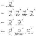
- a period allocated for each type of queue is referred to as a “phase”.
- FIG. 4 shows an example of setting the type of queue to be processed in each phase, the upper limit number of command processing and the time limit in each phase.
- the period is divided into five periods from phase 1 to phase 5, and the transition is made in a cycle of phases 1, 2, 3, 4, 5, 1, 2,.
- the processing target is a read-only queue for NSIDb, that is, three queues 52, 54, and 56 in the example of FIG. Among these queues, the queue with higher urgency is given priority for processing.
- the upper limit of command processing is 50.
- the number of commands is counted with one unit of access to data of a predetermined size. The same applies to the following description.
- phase 5 a time limit is provided so that even during the processing, the process can be temporarily interrupted and shifted to another phase.
- the time limit for phase 5 is set to “3.0 msec”.
- phase 5 processing may be interrupted when a command is stored in a highly urgent queue, for example, the emergency read queue 52 in FIG.
- phase 5 when the process of phase 5 is interrupted, the phase may be shifted to skip phase 2 and phase 3 until the interrupted process is completed.
- FIG. 5 is a flowchart showing a procedure of processing in which the command processing unit 46 reads data from NSIDb in phase 1 and phase 4.
- the read-only queue is divided into three according to the level of urgency as shown in FIG.
- S10 a command is stored in the most urgent queue (emergency read queue 52 in FIG. 3)
- S12 the command processing unit 46 reads out the data in the corresponding area by reading the command stored first in the queue, converting the logical address into a physical address, etc.
- commands are stored in the most urgent queue, they are read and processed sequentially (Y in S10, S12). If there is no command to be processed in the queue (N in S10) and the number of commands processed so far is less than the set processing upper limit (Y in S14), the next most urgent queue (high in FIG. 3) It is confirmed whether or not a command is stored in the priority read queue 54) (S16). If it is stored (Y in S16), the command processing unit 46 reads the command stored first in the queue, and reads the data in the same manner as described above (S18).
- the command processing unit 46 If it is stored (Y in S22), the command processing unit 46 reads the command stored first in the queue and reads the data in the same manner as described above (S24). If the processing upper limit number thus set is not reached (Y in S20), the command processing unit 46 again checks whether or not the command is stored in the most urgent queue each time one command is processed. If it is confirmed and stored, it is processed (Y in S10, S12). If the number of processed commands reaches the upper limit due to any processing in such a cycle (N in S14 or N in S20) or there are no more commands to be processed (N in S22), the phase is terminated and the next Move to the next phase.
- queues with higher urgency can be monitored more frequently and commands can be processed first, and the delay time from command storage to processing can be minimized.
- the time required for the entire phase and the bandwidth can be controlled by postponing the processing with the upper limit of the number of processing as a constraint and transferring it to another phase.
- FIG. 6 is a flowchart showing a processing procedure in which the command processing unit 46 reads or writes data from / to NSIDa to c in phase 2.
- the command processing unit 46 checks whether or not a command is stored in a queue for high-speed writing with respect to NSIDc (high-speed write queue 60 in FIG. 3) (S30). If stored (Y in S30), the command processing unit 46 reads the command stored first in the queue, converts the logical address into a physical address, and writes the data read from the system memory 14 to the corresponding area. (S32).
- phase is terminated and the process proceeds to the next phase (N in S34).
- N in S34 the setting of the upper limit number of processing shown in FIG. 4, since writing in phase 2 is limited to one command, this phase ends when the processing of S32 is performed once. If the number of processed commands is less than the upper limit of the set write processing (Y in S34), it is confirmed again whether the command is stored in the queue for high-speed writing. If it is stored, it is processed (Y in S30, S32).
- phase is terminated and the process proceeds to the next phase (N in S34). If there is no command to be processed in the queue for high-speed writing (N in S30), a standard read / write queue for NSIDa to NSIDc (standard read / write queues 51 and 62 in FIG. 3, standard) It is confirmed whether the command is stored in any of the write queues 58) (S36).
- the command processing unit 46 If it is stored (Y in S36), the command processing unit 46 reads the command stored first in the queue, and writes or reads data in the same manner as described above (S38). In phase 2, since a process upper limit is set for each of the read process and the write process, each time one command is processed, the number of commands and the upper limit are compared for each process content. If the upper limit number of processing has not been reached (Y in S34), it is checked again whether the command is stored in the queue for high-speed writing, and if it is stored, it is processed (Y in S30). , S32).
- N in S30 If there is no command to be processed in the queue (N in S30), it is checked whether or not the command is stored in the standard read or write queue, and if it is stored, it is processed (S36). Y, S38). When the number of commands processed in the cycle reaches the upper limit or there are no more commands to be processed, the phase is terminated and the process proceeds to the next phase (N in S34 or N in S36). With such a processing procedure, high-speed writing can be preferentially processed. In the example of FIG. 3, there are three queues that are subject to confirmation processing in S36, but basically a round robin method in which these are confirmed in order and processed if there is a command may be used.
- FIG. 7 is a flowchart showing a processing procedure in which the command processing unit 46 performs the reading process in the management process in the phase 3.
- the command processing unit 46 stores commands in any of the queues (SLC ⁇ TLC copy queue 64, read disturb avoidance data copy queue 66, garbage collection queue 68 in FIG. 3) provided for management processing. (S40). If it is stored (Y in S40), the command processing unit 46 reads the command stored first in the queue, and executes only the process of reading the data (S42).
- the reading process is repeated (Y in S44, Y in S40, S42).
- the upper limit of processing is reached (N in S44) or when there is no command to be processed in any queue (N in S40)
- the phase is terminated and the process proceeds to the next phase.
- there are a plurality of queues (three in the example of FIG. 3) that are subject to confirmation processing in S40, these are basically confirmed in a round robin manner and processed if there is a command.
- phase 3 instead of setting the upper limit of the number of processes as an absolute value, it is possible to read only the amount written in phase 5.
- the command for writing to the SLC in the phase 2 is skipped and the process proceeds to the phase 3 so that the data copy to the TLC is performed first. Also in this case, necessary data reading is performed by performing phases 1 and 4 in order.
- FIG. 8 is a flowchart showing a processing procedure in which the command processing unit 46 performs the writing process and the data erasing in the management process in the phase 5. It should be noted that the management process command executed only in the read process in the phase 3 is left in the queue after being distinguished from others by setting a flag or the like. Alternatively, the management processing commands may be stored separately as a read command, a write command, and an erase command, and the read command processed in phase 3 may be deleted from the queue.
- the command processing unit 46 checks whether there is a command whose processing has been interrupted at the timing of the previous phase 5 (S50). As described above, since the process in phase 5 requires a relatively long time, when a command is stored in an urgent read queue or the time limit for phase 5 expires, the process is interrupted and the process proceeds to phase 1. The command whose processing has been interrupted is stored in another queue (not shown), or is left in the original queue in such a state that it can be identified.
- the process is resumed from the time when the command is interrupted (S54). If there is no interrupted command (N in S50), the command processing unit 46 checks whether or not the command is stored in any of the queues provided for the management process (S52). However, the target command here is a command for which only data reading is performed in phase 3. If there is no such command, the phase is terminated and the process proceeds to the next phase (N in S52). If there is a command (Y in S52), write processing of the command and data erasure processing as necessary are started (S54).
- the processing is continued while confirming whether the command is stored in the most urgent read queue for NSIDb or whether the time limit set in phase 5 has been reached (N in S56, N in S58, S60). N).
- the started process is interrupted and the process proceeds to the next phase (S62). In this case, the process proceeds to phase 1 and phase 4 and returns to phase 5 again to resume the interrupted process.
- the frequency of occurrence of management processing executed in phase 3 and phase 5 is affected by the number of commands executed in phase 1, phase 2 and phase 4.
- the process of copying SLC to TLC is performed in units of 3 pages.
- the bottom of the book can be adjusted by copying from the SLC to the TLC once every three periods. Therefore, the remaining 66% of time can be allocated to another management process.
- 1 block is 768 pages and 3 pages are copied per cycle in Phase 3 and Phase 5
- 1 block is copied in 256 cycles.
- a block copy is required once every 000 cycles. Assuming that one block copy requires 256 cycles as described above, the maximum time ratio required for management processing for avoiding read disturb is 256 / 10000 ⁇ 2.5%.
- the causal relationship between the number of commands issued from the host unit 12 and the occurrence of management processing is taken into consideration, and the upper limit number of commands processed in each phase is set with an appropriate balance, so that management processing is not broken down. Everything can be handled smoothly. Further, by appropriately switching the queues to be processed in each phase according to the processing contents and priority as described above, the delay time from the issue of each command to the processing can be controlled.
- the time for which the processing of the head command stored in the NSIDb queue is delayed by other processing can be suppressed to about 3.0 msec which is the time limit of phase 5 at the maximum.
- FIG. 9 is a diagram for explaining an example in which a rule for switching phases according to a notification from the host unit 12 is introduced as an example.
- the information processing apparatus repeats the process of drawing an image to be displayed immediately after using the data stored in the flash memory 20 in accordance with the frame display cycle of the display apparatus.
- the horizontal direction is the time axis. From the top, the frame n, frame n + 1, frame n + 2,... Are displayed on the display device, each frame is drawn, and each phase of memory access by the flash controller 18 is shown. It is shown as a rectangle.
- the black period in the uppermost display process corresponds to the vertical blanking period.
- the information processing apparatus mainly the host unit 12
- the drawing period of each frame the size of data to be read from the flash memory 20, and the required frequency thereof also differ.
- a white arrow (for example, arrow 80) that protrudes downward from the rectangle of the drawing period exemplifies the read command issuance timing from the host unit 12.
- the time-consuming processes of the management process are collectively performed, so that the delay of the reading process can be further suppressed during the drawing period.
- the host unit 12 notifies the flash controller 18 of the completion. In the figure, this timing is indicated by arrows 82a, 82b, 82c, and 82d.
- the flash controller 18 proceeds from phase 4 to phase 5 on the condition that the notification has been received.
- this timing is indicated by arrows 84a, 84b, 84c and 84d.
- the process required by the host unit 12 and the process required by the flash memory 20 itself are performed by switching the type of command processed by the flash controller 18 in accordance with the progress of the process in the host unit 12. , Can be implemented at a timing suitable for each.
- command processing is limited to phases 1 to 4, so the delay time of the reading process is At most, it will be enough for Phase 2 and Phase 3.
- the delay time is a maximum of 0.9 msec.
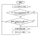
- FIG. 10 is a flowchart showing a processing procedure of the flash controller 18 focusing on the adjustment by the command adjustment unit 50.
- the command receiving unit 40, the management command generating unit 42, and the command processing unit 46 of the flash controller 18 receive a command issued from the host unit 12 or generate a command for management processing as described above. Or sequentially processing (S70). As described in detail above, this step includes processing for switching phases 1 to 5 and queues to be processed in each phase according to the rules set in the switching rule storage unit 48.
- an operation of shifting to phase 5 on condition of a notification from the host unit 12 may be included.
- the command adjustment unit 50 monitors whether or not the number of reads to the same block in the flash memory 20 exceeds a predetermined threshold (S72). Further, it is monitored whether or not the number of newly writable blocks has become a predetermined threshold value or less (S74). The former predicts in advance the timing of issuing a data copy command for avoiding read disturb.
- the latter predicts in advance the arrival timing of the garbage collection command. If neither monitoring result is NO, no adjustment is made by the command adjustment unit 50, and the command processing is continued (N in S72, N in S74, S70). If the number of reads to the same block exceeds a predetermined threshold value (Y in S72) or the number of newly writable blocks is equal to or smaller than the predetermined threshold value (Y in S74), the command adjustment unit 50 Adjusts one of the switching rules stored in the switching rule storage unit 48 (S76).
- Phase 1 For example, in Phase 1, Phase 2, and Phase 4, commands stored in the normal priority read queue, standard write and read queues are temporarily not processed, and the number of processes is limited. Increase the processing upper limit number and time limit of 3 and Phase 5. This increases the proportion of time available for management processing per cycle.
- the command adjustment unit 50 indicates that the number of reads to the same block has exceeded a predetermined threshold, or that the number of newly writable blocks has become equal to or less than the predetermined threshold. (S78).
- the host unit 12 temporarily reduces the number of commands issued for normal priority read processing, standard write processing, and read processing. Even if it does in this way, the ratio of the time which can be used for a management process will increase with respect to 1 period similarly to the change of a switching rule. Note that the host unit 12 may be notified of the number of reads and the number of writable blocks for the same block as needed, and the number of commands issued may be adjusted on the host unit 12 side.
- the necessity of adjustment may be determined by setting a threshold for the number of commands actually stored in the management processing queue, or by predicting the number of stored commands from the storage status of commands until then. .
- the command adjustment unit 50 restores the switching rule, or notifies the host unit to that effect and indicates the number of commands issued in the normal state. Or return to
- the access request to the flash memory is stored in different queues according to the contents of processing such as reading and writing and the priority in the processing. Then, according to the rules set for each queue, the target queue is switched to read and process the command. This makes it possible to process access requests in an order and frequency suitable for the characteristics of information processing, such as which of data read and write is dominant, which is more restrictive with respect to time, and which are equal.
- a plurality of queues are classified and a period (phase) for processing each type is provided.
- a switching rule between queues processed in the same phase and a switching rule between phases are imposed twice, and by combining them, fine setting, and flexible according to the actual situation. Operation becomes possible.
- queues for management processing such as garbage collection, data copy for avoiding read disturbance, and data copy from SLC to TLC are also incorporated.
- management processing such as garbage collection, data copy for avoiding read disturbance, and data copy from SLC to TLC are also incorporated.
- the management process described above occurs depending on the content and frequency of access requests from the host unit. Therefore, rules using absolute indicators are set for each queue, such as the upper limit of command processing and the time limit. By doing so, the balance between the two can be optimized and necessary processing can be performed with low delay without failure. Further, by circulating the phases, it becomes easy to estimate the processing period and the bandwidth can be controlled.
- management processing is not frequently performed, there is a processing having a unique property that takes a lot of time once the necessity arises.
- the timing at which such processing is started is predicted in advance, and the switching rule is temporarily changed, or issuance of less urgent requests from the host unit is suppressed.
- it is possible to easily implement a flexible response such as temporarily increasing the time allocated to the management process and promoting the access process necessary for the processing of the host unit.
- the present invention can be used for an information processing apparatus and a memory controller that perform memory access.
Landscapes
- Engineering & Computer Science (AREA)
- Theoretical Computer Science (AREA)
- Physics & Mathematics (AREA)
- General Engineering & Computer Science (AREA)
- General Physics & Mathematics (AREA)
- Human Computer Interaction (AREA)
- Memory System (AREA)
- Information Retrieval, Db Structures And Fs Structures Therefor (AREA)
- Techniques For Improving Reliability Of Storages (AREA)
Priority Applications (4)
| Application Number | Priority Date | Filing Date | Title |
|---|---|---|---|
| CN201780077153.8A CN110073337B (zh) | 2016-12-20 | 2017-12-13 | 信息处理装置和存储器访问方法 |
| KR1020197016557A KR102246840B1 (ko) | 2016-12-20 | 2017-12-13 | 정보 처리 장치, 메모리 액세스 방법 및 컴퓨터 프로그램 |
| EP17883337.2A EP3561678B1 (en) | 2016-12-20 | 2017-12-13 | Information processing device and memory access method |
| US16/346,717 US11281572B2 (en) | 2016-12-20 | 2017-12-13 | Information processing apparatus and memory access method |
Applications Claiming Priority (2)
| Application Number | Priority Date | Filing Date | Title |
|---|---|---|---|
| JP2016-247049 | 2016-12-20 | ||
| JP2016247049A JP6677627B2 (ja) | 2016-12-20 | 2016-12-20 | 情報処理装置およびメモリアクセス方法 |
Publications (1)
| Publication Number | Publication Date |
|---|---|
| WO2018116937A1 true WO2018116937A1 (ja) | 2018-06-28 |
Family
ID=62626406
Family Applications (1)
| Application Number | Title | Priority Date | Filing Date |
|---|---|---|---|
| PCT/JP2017/044777 WO2018116937A1 (ja) | 2016-12-20 | 2017-12-13 | 情報処理装置およびメモリアクセス方法 |
Country Status (7)
| Country | Link |
|---|---|
| US (1) | US11281572B2 (zh) |
| EP (1) | EP3561678B1 (zh) |
| JP (1) | JP6677627B2 (zh) |
| KR (1) | KR102246840B1 (zh) |
| CN (1) | CN110073337B (zh) |
| TW (1) | TWI662418B (zh) |
| WO (1) | WO2018116937A1 (zh) |
Cited By (2)
| Publication number | Priority date | Publication date | Assignee | Title |
|---|---|---|---|---|
| JP2021009676A (ja) * | 2019-06-28 | 2021-01-28 | エスケーハイニックス株式会社SK hynix Inc. | メモリシステム、メモリコントローラ及びその保存方法 |
| JP2022046413A (ja) * | 2020-09-10 | 2022-03-23 | ウェスタン デジタル テクノロジーズ インコーポレーテッド | 記憶デバイスのための改良された先読み能力 |
Families Citing this family (6)
| Publication number | Priority date | Publication date | Assignee | Title |
|---|---|---|---|---|
| US11061822B2 (en) * | 2018-08-27 | 2021-07-13 | Qualcomm Incorporated | Method, apparatus, and system for reducing pipeline stalls due to address translation misses |
| CN111124254B (zh) * | 2018-10-30 | 2023-09-29 | 伊姆西Ip控股有限责任公司 | 调度存储空间回收请求的方法、电子设备和程序产品 |
| CN110362275B (zh) * | 2019-07-10 | 2021-09-07 | 深圳大普微电子科技有限公司 | 提升固态硬盘服务质量的方法及固态硬盘 |
| US11029874B2 (en) * | 2019-07-30 | 2021-06-08 | Western Digital Technologies, Inc. | Rolling XOR protection in efficient pipeline |
| JP2021086583A (ja) * | 2019-11-29 | 2021-06-03 | キヤノン株式会社 | 情報処理装置、制御装置および制御装置の制御方法 |
| US20220004337A1 (en) * | 2020-07-06 | 2022-01-06 | Micron Technology, Inc. | Command prioritization in a command queue |
Citations (4)
| Publication number | Priority date | Publication date | Assignee | Title |
|---|---|---|---|---|
| JP2006185198A (ja) * | 2004-12-28 | 2006-07-13 | Kyocera Mita Corp | メモリアクセス制御回路 |
| JP2006236056A (ja) * | 2005-02-25 | 2006-09-07 | Sony Corp | 情報処理装置および方法、メモリ制御装置および方法、記録媒体、並びにプログラム |
| JP2013200692A (ja) * | 2012-03-23 | 2013-10-03 | Toshiba Corp | メモリシステム |
| WO2014132346A1 (ja) | 2013-02-27 | 2014-09-04 | 株式会社日立製作所 | 半導体ストレージ |
Family Cites Families (27)
| Publication number | Priority date | Publication date | Assignee | Title |
|---|---|---|---|---|
| US6570876B1 (en) * | 1998-04-01 | 2003-05-27 | Hitachi, Ltd. | Packet switch and switching method for switching variable length packets |
| JP2000285082A (ja) | 1999-03-31 | 2000-10-13 | Toshiba Corp | 中央演算装置及びコンパイル方法 |
| US20060184718A1 (en) * | 2005-02-16 | 2006-08-17 | Sinclair Alan W | Direct file data programming and deletion in flash memories |
| JP4142068B2 (ja) * | 2006-06-16 | 2008-08-27 | 株式会社ソニー・コンピュータエンタテインメント | 情報処理装置およびアクセス制御方法 |
| US8208406B1 (en) * | 2008-03-25 | 2012-06-26 | Juniper Networks, Inc. | Packet forwarding using feedback controlled weighted queues dynamically adjusted based on processor utilization |
| JP5147584B2 (ja) * | 2008-07-23 | 2013-02-20 | 株式会社日立製作所 | ストレージサブシステム及びコントローラによるコマンド実行方法 |
| JP2010176646A (ja) * | 2009-02-02 | 2010-08-12 | Toshiba Information Systems (Japan) Corp | メモリシステムおよびメモリシステムのインターリーブ制御方法 |
| CN101498994B (zh) * | 2009-02-16 | 2011-04-20 | 华中科技大学 | 一种固态硬盘控制器 |
| US8688894B2 (en) * | 2009-09-03 | 2014-04-01 | Pioneer Chip Technology Ltd. | Page based management of flash storage |
| US8595411B2 (en) * | 2009-12-30 | 2013-11-26 | Sandisk Technologies Inc. | Method and controller for performing a sequence of commands |
| US8838853B2 (en) * | 2010-01-18 | 2014-09-16 | Marvell International Ltd. | Access buffer |
| US8468318B2 (en) | 2010-09-15 | 2013-06-18 | Pure Storage Inc. | Scheduling of I/O writes in a storage environment |
| US8271692B1 (en) * | 2010-10-01 | 2012-09-18 | Western Digital Technologies, Inc. | Throttled command completion time |
| US20120246385A1 (en) * | 2011-03-22 | 2012-09-27 | American Megatrends, Inc. | Emulating spi or 12c prom/eprom/eeprom using flash memory of microcontroller |
| US8700834B2 (en) * | 2011-09-06 | 2014-04-15 | Western Digital Technologies, Inc. | Systems and methods for an enhanced controller architecture in data storage systems |
| US8996782B2 (en) * | 2012-03-23 | 2015-03-31 | Kabushiki Kaisha Toshiba | Memory system and bank interleaving method |
| US9058208B2 (en) | 2012-11-12 | 2015-06-16 | Skymedi Corporation | Method of scheduling tasks for memories and memory system thereof |
| CN103488578B (zh) * | 2012-12-28 | 2016-05-25 | 晶天电子(深圳)有限公司 | 虚拟存储设备(vmd)应用/驱动器 |
| US8959263B2 (en) * | 2013-01-08 | 2015-02-17 | Apple Inc. | Maintaining I/O priority and I/O sorting |
| US9268495B2 (en) * | 2013-03-15 | 2016-02-23 | Apple Inc. | Managing I/O priorities |
| WO2015145552A1 (ja) * | 2014-03-24 | 2015-10-01 | 株式会社日立製作所 | 不揮発メモリデバイス、及び、不揮発メモリデバイスを有するストレージ装置 |
| US10073714B2 (en) | 2015-03-11 | 2018-09-11 | Western Digital Technologies, Inc. | Task queues |
| TWI588652B (zh) * | 2015-09-01 | 2017-06-21 | 慧榮科技股份有限公司 | 讀取及寫入命令排程方法以及使用該方法的裝置 |
| US10866910B2 (en) * | 2015-09-28 | 2020-12-15 | Sandisk Technologies Llc | Systems, methods, and computer-readable media for managing instruction fetch in virtual computing environments |
| US9910772B2 (en) * | 2016-04-27 | 2018-03-06 | Silicon Motion Inc. | Flash memory apparatus and storage management method for flash memory |
| JP6783645B2 (ja) * | 2016-12-21 | 2020-11-11 | キオクシア株式会社 | メモリシステムおよび制御方法 |
| US10831403B2 (en) * | 2017-05-19 | 2020-11-10 | Seagate Technology Llc | Probabalistic command aging and selection |
-
2016
- 2016-12-20 JP JP2016247049A patent/JP6677627B2/ja active Active
-
2017
- 2017-10-26 TW TW106136823A patent/TWI662418B/zh active
- 2017-12-13 CN CN201780077153.8A patent/CN110073337B/zh active Active
- 2017-12-13 EP EP17883337.2A patent/EP3561678B1/en active Active
- 2017-12-13 US US16/346,717 patent/US11281572B2/en active Active
- 2017-12-13 KR KR1020197016557A patent/KR102246840B1/ko active IP Right Grant
- 2017-12-13 WO PCT/JP2017/044777 patent/WO2018116937A1/ja unknown
Patent Citations (4)
| Publication number | Priority date | Publication date | Assignee | Title |
|---|---|---|---|---|
| JP2006185198A (ja) * | 2004-12-28 | 2006-07-13 | Kyocera Mita Corp | メモリアクセス制御回路 |
| JP2006236056A (ja) * | 2005-02-25 | 2006-09-07 | Sony Corp | 情報処理装置および方法、メモリ制御装置および方法、記録媒体、並びにプログラム |
| JP2013200692A (ja) * | 2012-03-23 | 2013-10-03 | Toshiba Corp | メモリシステム |
| WO2014132346A1 (ja) | 2013-02-27 | 2014-09-04 | 株式会社日立製作所 | 半導体ストレージ |
Non-Patent Citations (1)
| Title |
|---|
| See also references of EP3561678A4 |
Cited By (4)
| Publication number | Priority date | Publication date | Assignee | Title |
|---|---|---|---|---|
| JP2021009676A (ja) * | 2019-06-28 | 2021-01-28 | エスケーハイニックス株式会社SK hynix Inc. | メモリシステム、メモリコントローラ及びその保存方法 |
| JP7050839B2 (ja) | 2019-06-28 | 2022-04-08 | エスケーハイニックス株式会社 | メモリシステム、メモリコントローラ及びその保存方法 |
| JP2022046413A (ja) * | 2020-09-10 | 2022-03-23 | ウェスタン デジタル テクノロジーズ インコーポレーテッド | 記憶デバイスのための改良された先読み能力 |
| JP7170093B2 (ja) | 2020-09-10 | 2022-11-11 | ウェスタン デジタル テクノロジーズ インコーポレーテッド | 記憶デバイスのための改良された先読み能力 |
Also Published As
| Publication number | Publication date |
|---|---|
| EP3561678A1 (en) | 2019-10-30 |
| US20200073793A1 (en) | 2020-03-05 |
| CN110073337A (zh) | 2019-07-30 |
| JP2018101301A (ja) | 2018-06-28 |
| EP3561678A4 (en) | 2020-08-05 |
| CN110073337B (zh) | 2023-06-02 |
| TW201824010A (zh) | 2018-07-01 |
| KR102246840B1 (ko) | 2021-04-30 |
| TWI662418B (zh) | 2019-06-11 |
| US11281572B2 (en) | 2022-03-22 |
| JP6677627B2 (ja) | 2020-04-08 |
| EP3561678B1 (en) | 2023-05-17 |
| KR20190079672A (ko) | 2019-07-05 |
Similar Documents
| Publication | Publication Date | Title |
|---|---|---|
| WO2018116937A1 (ja) | 情報処理装置およびメモリアクセス方法 | |
| JP7366795B2 (ja) | メモリシステムおよび制御方法 | |
| US9244617B2 (en) | Scheduling requests in a solid state memory device | |
| KR101563875B1 (ko) | 호스트 기록 작업과 캐시 플러싱을 균형화하기 위한 방법과 시스템 | |
| US8171239B2 (en) | Storage management method and system using the same | |
| US11704239B2 (en) | Garbage collection method for storage medium, storage medium, and program product | |
| US9251055B2 (en) | Memory system and control method of memory system | |
| JP4429780B2 (ja) | 記憶制御装置、制御方法、および制御プログラム。 | |
| US9696934B2 (en) | Hybrid solid state drive (SSD) using PCM or other high performance solid-state memory | |
| US20090157974A1 (en) | System And Method For Clearing Data From A Cache | |
| CN103838676B (zh) | 数据存储系统、数据存储方法及pcm桥 | |
| US20170003911A1 (en) | Information processing device | |
| KR20200110547A (ko) | 스토리지 장치 및 스토리지 장치를 포함하는 컴퓨팅 장치 | |
| JP2019046238A (ja) | メモリシステム | |
| US10872015B2 (en) | Data storage system with strategic contention avoidance | |
| JP5687649B2 (ja) | 半導体記憶装置の制御方法 | |
| US20190034121A1 (en) | Information processing apparatus, method and non-transitory computer-readable storage medium | |
| CN113467713A (zh) | 数据分离方法及固态硬盘 | |
| JP3934659B1 (ja) | メモリコントローラ及びフラッシュメモリシステム | |
| KR20090036900A (ko) | 플래시 메모리의 데이터 관리방법 | |
| JP2017134446A (ja) | メモリ制御装置、記憶装置、メモリ制御方法およびコンピュータプログラム | |
| JP2016115081A (ja) | 不揮発メモリストレージ制御装置、不揮発メモリストレージの書き込み制御方法およびプログラム |
Legal Events
| Date | Code | Title | Description |
|---|---|---|---|
| 121 | Ep: the epo has been informed by wipo that ep was designated in this application |
Ref document number: 17883337 Country of ref document: EP Kind code of ref document: A1 |
|
| ENP | Entry into the national phase |
Ref document number: 20197016557 Country of ref document: KR Kind code of ref document: A |
|
| NENP | Non-entry into the national phase |
Ref country code: DE |
|
| ENP | Entry into the national phase |
Ref document number: 2017883337 Country of ref document: EP Effective date: 20190722 |