JP6677627B2 - 情報処理装置およびメモリアクセス方法 - Google Patents
情報処理装置およびメモリアクセス方法 Download PDFInfo
- Publication number
- JP6677627B2 JP6677627B2 JP2016247049A JP2016247049A JP6677627B2 JP 6677627 B2 JP6677627 B2 JP 6677627B2 JP 2016247049 A JP2016247049 A JP 2016247049A JP 2016247049 A JP2016247049 A JP 2016247049A JP 6677627 B2 JP6677627 B2 JP 6677627B2
- Authority
- JP
- Japan
- Prior art keywords
- queue
- command
- request
- processing
- queues
- Prior art date
- Legal status (The legal status is an assumption and is not a legal conclusion. Google has not performed a legal analysis and makes no representation as to the accuracy of the status listed.)
- Active
Links
Images


Classifications
-
- G—PHYSICS
- G06—COMPUTING; CALCULATING OR COUNTING
- G06F—ELECTRIC DIGITAL DATA PROCESSING
- G06F12/00—Accessing, addressing or allocating within memory systems or architectures
- G06F12/02—Addressing or allocation; Relocation
- G06F12/0223—User address space allocation, e.g. contiguous or non contiguous base addressing
- G06F12/023—Free address space management
- G06F12/0238—Memory management in non-volatile memory, e.g. resistive RAM or ferroelectric memory
- G06F12/0246—Memory management in non-volatile memory, e.g. resistive RAM or ferroelectric memory in block erasable memory, e.g. flash memory
-
- G—PHYSICS
- G06—COMPUTING; CALCULATING OR COUNTING
- G06F—ELECTRIC DIGITAL DATA PROCESSING
- G06F12/00—Accessing, addressing or allocating within memory systems or architectures
-
- G—PHYSICS
- G06—COMPUTING; CALCULATING OR COUNTING
- G06F—ELECTRIC DIGITAL DATA PROCESSING
- G06F12/00—Accessing, addressing or allocating within memory systems or architectures
- G06F12/02—Addressing or allocation; Relocation
-
- G—PHYSICS
- G06—COMPUTING; CALCULATING OR COUNTING
- G06F—ELECTRIC DIGITAL DATA PROCESSING
- G06F13/00—Interconnection of, or transfer of information or other signals between, memories, input/output devices or central processing units
- G06F13/14—Handling requests for interconnection or transfer
- G06F13/16—Handling requests for interconnection or transfer for access to memory bus
- G06F13/1605—Handling requests for interconnection or transfer for access to memory bus based on arbitration
- G06F13/1642—Handling requests for interconnection or transfer for access to memory bus based on arbitration with request queuing
-
- G—PHYSICS
- G06—COMPUTING; CALCULATING OR COUNTING
- G06F—ELECTRIC DIGITAL DATA PROCESSING
- G06F3/00—Input arrangements for transferring data to be processed into a form capable of being handled by the computer; Output arrangements for transferring data from processing unit to output unit, e.g. interface arrangements
- G06F3/06—Digital input from, or digital output to, record carriers, e.g. RAID, emulated record carriers or networked record carriers
- G06F3/0601—Interfaces specially adapted for storage systems
- G06F3/0602—Interfaces specially adapted for storage systems specifically adapted to achieve a particular effect
- G06F3/061—Improving I/O performance
- G06F3/0611—Improving I/O performance in relation to response time
-
- G—PHYSICS
- G06—COMPUTING; CALCULATING OR COUNTING
- G06F—ELECTRIC DIGITAL DATA PROCESSING
- G06F3/00—Input arrangements for transferring data to be processed into a form capable of being handled by the computer; Output arrangements for transferring data from processing unit to output unit, e.g. interface arrangements
- G06F3/06—Digital input from, or digital output to, record carriers, e.g. RAID, emulated record carriers or networked record carriers
- G06F3/0601—Interfaces specially adapted for storage systems
- G06F3/0628—Interfaces specially adapted for storage systems making use of a particular technique
- G06F3/0638—Organizing or formatting or addressing of data
- G06F3/064—Management of blocks
-
- G—PHYSICS
- G06—COMPUTING; CALCULATING OR COUNTING
- G06F—ELECTRIC DIGITAL DATA PROCESSING
- G06F3/00—Input arrangements for transferring data to be processed into a form capable of being handled by the computer; Output arrangements for transferring data from processing unit to output unit, e.g. interface arrangements
- G06F3/06—Digital input from, or digital output to, record carriers, e.g. RAID, emulated record carriers or networked record carriers
- G06F3/0601—Interfaces specially adapted for storage systems
- G06F3/0628—Interfaces specially adapted for storage systems making use of a particular technique
- G06F3/0646—Horizontal data movement in storage systems, i.e. moving data in between storage devices or systems
- G06F3/0647—Migration mechanisms
- G06F3/0649—Lifecycle management
-
- G—PHYSICS
- G06—COMPUTING; CALCULATING OR COUNTING
- G06F—ELECTRIC DIGITAL DATA PROCESSING
- G06F3/00—Input arrangements for transferring data to be processed into a form capable of being handled by the computer; Output arrangements for transferring data from processing unit to output unit, e.g. interface arrangements
- G06F3/06—Digital input from, or digital output to, record carriers, e.g. RAID, emulated record carriers or networked record carriers
- G06F3/0601—Interfaces specially adapted for storage systems
- G06F3/0628—Interfaces specially adapted for storage systems making use of a particular technique
- G06F3/0655—Vertical data movement, i.e. input-output transfer; data movement between one or more hosts and one or more storage devices
- G06F3/0658—Controller construction arrangements
-
- G—PHYSICS
- G06—COMPUTING; CALCULATING OR COUNTING
- G06F—ELECTRIC DIGITAL DATA PROCESSING
- G06F3/00—Input arrangements for transferring data to be processed into a form capable of being handled by the computer; Output arrangements for transferring data from processing unit to output unit, e.g. interface arrangements
- G06F3/06—Digital input from, or digital output to, record carriers, e.g. RAID, emulated record carriers or networked record carriers
- G06F3/0601—Interfaces specially adapted for storage systems
- G06F3/0628—Interfaces specially adapted for storage systems making use of a particular technique
- G06F3/0655—Vertical data movement, i.e. input-output transfer; data movement between one or more hosts and one or more storage devices
- G06F3/0659—Command handling arrangements, e.g. command buffers, queues, command scheduling
-
- G—PHYSICS
- G06—COMPUTING; CALCULATING OR COUNTING
- G06F—ELECTRIC DIGITAL DATA PROCESSING
- G06F3/00—Input arrangements for transferring data to be processed into a form capable of being handled by the computer; Output arrangements for transferring data from processing unit to output unit, e.g. interface arrangements
- G06F3/06—Digital input from, or digital output to, record carriers, e.g. RAID, emulated record carriers or networked record carriers
- G06F3/0601—Interfaces specially adapted for storage systems
- G06F3/0668—Interfaces specially adapted for storage systems adopting a particular infrastructure
- G06F3/0671—In-line storage system
- G06F3/0673—Single storage device
- G06F3/0679—Non-volatile semiconductor memory device, e.g. flash memory, one time programmable memory [OTP]
Description
Claims (17)
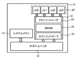
- ホストプロセッサからメモリへのアクセス要求を受け付けるコマンド受付部と、
前記アクセス要求が分類して格納された複数のキューのいずれかから前記アクセス要求を読み出し、実行するコマンド処理部と、
を含むメモリコントローラを備え、
前記コマンド処理部は、前記複数のキューを分類してなるグループ内で、前記キューごとに設定された規則に応じたタイミングで、前記複数のキューのうち要求読み出し先のキューを次へ切り替えるとともに、前記グループごとに設定された処理の制限に基づくタイミングで、前記要求読み出し先のキューを次のグループへ切り替えることを特徴とする情報処理装置。 - 前記複数のキューは、アクセスの内容および優先度によって分類された前記アクセス要求をそれぞれ格納するとともに、当該アクセスの内容によって前記グループに分けられ、
前記コマンド処理部は、前記グループごとに独立して設定された処理上限数または制限時間に到達した時点で、前記要求読み出し先のキューを次のグループへ切り替えることを特徴とする請求項1に記載の情報処理装置。 - 前記コマンド処理部は、前記優先度によって設定された規則に応じたタイミングで、読み出し先のキューを前記グループ内で切り替えることを特徴とする請求項2に記載の情報処理装置。
- 前記メモリコントローラは、前記メモリの管理に必要な処理の要求を発行する管理コマンド生成部をさらに備え、
前記複数のキューはさらに、前記管理コマンド生成部が発行した管理用処理の要求を格納するキューを含み、
前記コマンド処理部は、前記キューから、前記管理用処理の要求を読み出してさらに実行することを特徴とする請求項1から3のいずれかに記載の情報処理装置。 - 前記コマンド処理部は、前記管理用処理の要求を格納するキューを読み出し先としている際、設定された制限時間を経過したタイミングで、要求読み出し先を次のキューへ切り替えることを特徴とする請求項4に記載の情報処理装置。
- 前記コマンド処理部は、前記管理用処理の要求を格納するキューを読み出し先としている際、別のキューに所定の優先度を有するアクセス要求が格納されたタイミングで、要求読み出し先を当該別のキューへ切り替えることを特徴とする請求項4または5に記載の情報処理装置。
- 前記コマンド処理部は、前記ホストプロセッサが通知したタイミングで、前記管理用処理の要求を格納するキューを要求読み出し先とすることを特徴とする請求項4から5のいずれかに記載の情報処理装置。
- 前記コマンド処理部は、前記管理用処理のうち読み出し処理の要求を読み出す期間と、書き込み処理の要求を読み出す期間を分離することを特徴とする請求項4から7のいずれかに記載の情報処理装置。
- 前記管理用処理は、あるブロックに格納されたデータを別のブロックに待避させたうえで元のブロックのデータを消去する処理を含むことを特徴とする請求項4から8のいずれかに記載の情報処理装置。
- 前記管理用処理は、1メモリセル当たり1ビットを記録するSLC(Single Level Cell)領域に書き込まれたデータを、1メモリセル当たり3ビットを記録するTLC(Triple Level Cell)領域にコピーする処理を含むことを特徴とする請求項4から8のいずれかに記載の情報処理装置。
- 前記メモリコントローラは、前記キューに格納済みの前記管理用処理の要求量および、前記管理用処理の要求が発行されるタイミングの予測結果の少なくともいずれかに基づき、前記キューごとに設定された規則および前記グループごとに設定された処理の制限の少なくともいずれかを変更するコマンド調整部をさらに備えたことを特徴とする請求項4から10のいずれかに記載の情報処理装置。
- 前記メモリコントローラは、前記キューに格納済みの前記管理用処理の要求量および、前記管理用処理の要求が発行されるタイミングの予測結果の少なくともいずれかに基づき、前記ホストプロセッサへアクセス要求の発行制御を依頼するコマンド調整部をさらに備えたことを特徴とする請求項4から10のいずれかに記載の情報処理装置。
- 前記コマンド処理部は、所定の基準以上の優先度を有する読み出し要求をまとめて格納するキューから、当該読み出し要求を順次読み出し、実行することを特徴とする請求項1から12のいずれかに記載の情報処理装置。
- 前記ホストプロセッサからのアクセス要求の対象となるデータを格納するNAND型フラッシュメモリをさらに備えたことを特徴とする請求項1から13のいずれかに記載の情報処理装置。
- 情報処理を実施し、前記メモリコントローラに前記メモリへのアクセス要求を発行するホストプロセッサをさらに備えたことを特徴とする請求項1から14のいずれかに記載の情報処理装置。
- ホストプロセッサからメモリへのアクセス要求を受け付けるステップと、
前記アクセス要求を分類して格納する複数のキューのいずれかから前記アクセス要求を読み出すステップと、
読み出したアクセス要求を実行するステップと、
を含み、
前記読み出すステップは、前記複数のキューを分類してなるグループ内で、前記キューごとに設定された規則に応じたタイミングで、前記複数のキューのうち要求読み出し先のキューを次へ切り替えるとともに、前記グループごとに設定された処理の制限に基づくタイミングで、前記要求読み出し先のキューを次のグループへ切り替えることを特徴とするメモリコントローラによるメモリアクセス方法。 - ホストプロセッサからメモリへのアクセス要求を受け付ける機能と、
前記アクセス要求が分類して格納された複数のキューのいずれかから前記アクセス要求を読み出し、実行する機能と、
をメモリコントローラに実現させるコンピュータプログラムであって、
前記実行する機能は、前記複数のキューを分類してなるグループ内で、前記キューごとに設定された規則に応じたタイミングで、前記複数のキューのうち要求読み出し先のキューを次へ切り替えるとともに、前記グループごとに設定された処理の制限に基づくタイミングで、前記要求読み出し先のキューを次のグループへ切り替えることを特徴とするコンピュータプログラム。
Priority Applications (7)
| Application Number | Priority Date | Filing Date | Title |
|---|---|---|---|
| JP2016247049A JP6677627B2 (ja) | 2016-12-20 | 2016-12-20 | 情報処理装置およびメモリアクセス方法 |
| TW106136823A TWI662418B (zh) | 2016-12-20 | 2017-10-26 | Information processing device and memory access method |
| PCT/JP2017/044777 WO2018116937A1 (ja) | 2016-12-20 | 2017-12-13 | 情報処理装置およびメモリアクセス方法 |
| EP17883337.2A EP3561678B1 (en) | 2016-12-20 | 2017-12-13 | Information processing device and memory access method |
| CN201780077153.8A CN110073337B (zh) | 2016-12-20 | 2017-12-13 | 信息处理装置和存储器访问方法 |
| KR1020197016557A KR102246840B1 (ko) | 2016-12-20 | 2017-12-13 | 정보 처리 장치, 메모리 액세스 방법 및 컴퓨터 프로그램 |
| US16/346,717 US11281572B2 (en) | 2016-12-20 | 2017-12-13 | Information processing apparatus and memory access method |
Applications Claiming Priority (1)
| Application Number | Priority Date | Filing Date | Title |
|---|---|---|---|
| JP2016247049A JP6677627B2 (ja) | 2016-12-20 | 2016-12-20 | 情報処理装置およびメモリアクセス方法 |
Publications (3)
| Publication Number | Publication Date |
|---|---|
| JP2018101301A JP2018101301A (ja) | 2018-06-28 |
| JP2018101301A5 JP2018101301A5 (ja) | 2019-02-21 |
| JP6677627B2 true JP6677627B2 (ja) | 2020-04-08 |
Family
ID=62626406
Family Applications (1)
| Application Number | Title | Priority Date | Filing Date |
|---|---|---|---|
| JP2016247049A Active JP6677627B2 (ja) | 2016-12-20 | 2016-12-20 | 情報処理装置およびメモリアクセス方法 |
Country Status (7)
| Country | Link |
|---|---|
| US (1) | US11281572B2 (ja) |
| EP (1) | EP3561678B1 (ja) |
| JP (1) | JP6677627B2 (ja) |
| KR (1) | KR102246840B1 (ja) |
| CN (1) | CN110073337B (ja) |
| TW (1) | TWI662418B (ja) |
| WO (1) | WO2018116937A1 (ja) |
Families Citing this family (8)
| Publication number | Priority date | Publication date | Assignee | Title |
|---|---|---|---|---|
| US11061822B2 (en) * | 2018-08-27 | 2021-07-13 | Qualcomm Incorporated | Method, apparatus, and system for reducing pipeline stalls due to address translation misses |
| CN111124254B (zh) * | 2018-10-30 | 2023-09-29 | 伊姆西Ip控股有限责任公司 | 调度存储空间回收请求的方法、电子设备和程序产品 |
| KR20210001414A (ko) * | 2019-06-28 | 2021-01-06 | 에스케이하이닉스 주식회사 | 메모리 시스템, 메모리 컨트롤러 및 그 저장 방법 |
| CN110362275B (zh) * | 2019-07-10 | 2021-09-07 | 深圳大普微电子科技有限公司 | 提升固态硬盘服务质量的方法及固态硬盘 |
| US11029874B2 (en) * | 2019-07-30 | 2021-06-08 | Western Digital Technologies, Inc. | Rolling XOR protection in efficient pipeline |
| JP2021086583A (ja) * | 2019-11-29 | 2021-06-03 | キヤノン株式会社 | 情報処理装置、制御装置および制御装置の制御方法 |
| US20220004337A1 (en) * | 2020-07-06 | 2022-01-06 | Micron Technology, Inc. | Command prioritization in a command queue |
| CN114168495A (zh) * | 2020-09-10 | 2022-03-11 | 西部数据技术公司 | 存储设备的增强的预读能力 |
Family Cites Families (31)
| Publication number | Priority date | Publication date | Assignee | Title |
|---|---|---|---|---|
| US6570876B1 (en) * | 1998-04-01 | 2003-05-27 | Hitachi, Ltd. | Packet switch and switching method for switching variable length packets |
| JP2000285082A (ja) * | 1999-03-31 | 2000-10-13 | Toshiba Corp | 中央演算装置及びコンパイル方法 |
| JP4327081B2 (ja) * | 2004-12-28 | 2009-09-09 | 京セラミタ株式会社 | メモリアクセス制御回路 |
| US20060184718A1 (en) * | 2005-02-16 | 2006-08-17 | Sinclair Alan W | Direct file data programming and deletion in flash memories |
| JP4419868B2 (ja) * | 2005-02-25 | 2010-02-24 | ソニー株式会社 | 情報処理装置および方法、メモリ制御装置および方法、記録媒体、並びにプログラム |
| JP4142068B2 (ja) * | 2006-06-16 | 2008-08-27 | 株式会社ソニー・コンピュータエンタテインメント | 情報処理装置およびアクセス制御方法 |
| US8208406B1 (en) * | 2008-03-25 | 2012-06-26 | Juniper Networks, Inc. | Packet forwarding using feedback controlled weighted queues dynamically adjusted based on processor utilization |
| JP5147584B2 (ja) * | 2008-07-23 | 2013-02-20 | 株式会社日立製作所 | ストレージサブシステム及びコントローラによるコマンド実行方法 |
| JP2010176646A (ja) * | 2009-02-02 | 2010-08-12 | Toshiba Information Systems (Japan) Corp | メモリシステムおよびメモリシステムのインターリーブ制御方法 |
| CN101498994B (zh) * | 2009-02-16 | 2011-04-20 | 华中科技大学 | 一种固态硬盘控制器 |
| US8688894B2 (en) | 2009-09-03 | 2014-04-01 | Pioneer Chip Technology Ltd. | Page based management of flash storage |
| US8595411B2 (en) * | 2009-12-30 | 2013-11-26 | Sandisk Technologies Inc. | Method and controller for performing a sequence of commands |
| US8838853B2 (en) * | 2010-01-18 | 2014-09-16 | Marvell International Ltd. | Access buffer |
| US8468318B2 (en) * | 2010-09-15 | 2013-06-18 | Pure Storage Inc. | Scheduling of I/O writes in a storage environment |
| US8271692B1 (en) * | 2010-10-01 | 2012-09-18 | Western Digital Technologies, Inc. | Throttled command completion time |
| US20120246385A1 (en) * | 2011-03-22 | 2012-09-27 | American Megatrends, Inc. | Emulating spi or 12c prom/eprom/eeprom using flash memory of microcontroller |
| US8700834B2 (en) * | 2011-09-06 | 2014-04-15 | Western Digital Technologies, Inc. | Systems and methods for an enhanced controller architecture in data storage systems |
| US8996782B2 (en) * | 2012-03-23 | 2015-03-31 | Kabushiki Kaisha Toshiba | Memory system and bank interleaving method |
| JP2013200692A (ja) * | 2012-03-23 | 2013-10-03 | Toshiba Corp | メモリシステム |
| US9058208B2 (en) * | 2012-11-12 | 2015-06-16 | Skymedi Corporation | Method of scheduling tasks for memories and memory system thereof |
| CN103488578B (zh) * | 2012-12-28 | 2016-05-25 | 晶天电子(深圳)有限公司 | 虚拟存储设备(vmd)应用/驱动器 |
| US8959263B2 (en) * | 2013-01-08 | 2015-02-17 | Apple Inc. | Maintaining I/O priority and I/O sorting |
| US20160011782A1 (en) | 2013-02-27 | 2016-01-14 | Hitachi, Ltd. | Semiconductor storage |
| US9268495B2 (en) * | 2013-03-15 | 2016-02-23 | Apple Inc. | Managing I/O priorities |
| US9898201B2 (en) * | 2014-03-24 | 2018-02-20 | Hitachi, Ltd. | Non-volatile memory device, and storage apparatus to reduce a read retry occurrence frequency and prevent read performance from lowering |
| US10073714B2 (en) * | 2015-03-11 | 2018-09-11 | Western Digital Technologies, Inc. | Task queues |
| TWI588652B (zh) * | 2015-09-01 | 2017-06-21 | 慧榮科技股份有限公司 | 讀取及寫入命令排程方法以及使用該方法的裝置 |
| US10866910B2 (en) * | 2015-09-28 | 2020-12-15 | Sandisk Technologies Llc | Systems, methods, and computer-readable media for managing instruction fetch in virtual computing environments |
| US9910772B2 (en) * | 2016-04-27 | 2018-03-06 | Silicon Motion Inc. | Flash memory apparatus and storage management method for flash memory |
| JP6783645B2 (ja) * | 2016-12-21 | 2020-11-11 | キオクシア株式会社 | メモリシステムおよび制御方法 |
| US10831403B2 (en) * | 2017-05-19 | 2020-11-10 | Seagate Technology Llc | Probabalistic command aging and selection |
-
2016
- 2016-12-20 JP JP2016247049A patent/JP6677627B2/ja active Active
-
2017
- 2017-10-26 TW TW106136823A patent/TWI662418B/zh active
- 2017-12-13 WO PCT/JP2017/044777 patent/WO2018116937A1/ja unknown
- 2017-12-13 CN CN201780077153.8A patent/CN110073337B/zh active Active
- 2017-12-13 EP EP17883337.2A patent/EP3561678B1/en active Active
- 2017-12-13 US US16/346,717 patent/US11281572B2/en active Active
- 2017-12-13 KR KR1020197016557A patent/KR102246840B1/ko active IP Right Grant
Also Published As
| Publication number | Publication date |
|---|---|
| US20200073793A1 (en) | 2020-03-05 |
| EP3561678A1 (en) | 2019-10-30 |
| US11281572B2 (en) | 2022-03-22 |
| JP2018101301A (ja) | 2018-06-28 |
| EP3561678B1 (en) | 2023-05-17 |
| KR20190079672A (ko) | 2019-07-05 |
| WO2018116937A1 (ja) | 2018-06-28 |
| CN110073337A (zh) | 2019-07-30 |
| TWI662418B (zh) | 2019-06-11 |
| CN110073337B (zh) | 2023-06-02 |
| TW201824010A (zh) | 2018-07-01 |
| KR102246840B1 (ko) | 2021-04-30 |
| EP3561678A4 (en) | 2020-08-05 |
Similar Documents
| Publication | Publication Date | Title |
|---|---|---|
| JP6677627B2 (ja) | 情報処理装置およびメモリアクセス方法 | |
| US9244617B2 (en) | Scheduling requests in a solid state memory device | |
| US11704239B2 (en) | Garbage collection method for storage medium, storage medium, and program product | |
| JP7366795B2 (ja) | メモリシステムおよび制御方法 | |
| US20200004674A1 (en) | Non-deterministic window scheduling for data storage systems | |
| KR101563875B1 (ko) | 호스트 기록 작업과 캐시 플러싱을 균형화하기 위한 방법과 시스템 | |
| US8171239B2 (en) | Storage management method and system using the same | |
| CN102713866B (zh) | 减少基于闪存的存储系统中的存取争用 | |
| US10789160B2 (en) | Utilizing different data storage policies in response to different characteristics of data | |
| US20170160953A1 (en) | Data storage device that stabilizes write latency | |
| JP2005293205A (ja) | 記憶制御装置、制御方法、および制御プログラム。 | |
| JP2011145838A (ja) | 記憶装置管理装置および記憶装置の管理方法 | |
| US20170003911A1 (en) | Information processing device | |
| CN106598504B (zh) | 数据存储方法及装置 | |
| JP2019046238A (ja) | メモリシステム | |
| JP2011209963A (ja) | メモリ制御装置及びメモリ制御方法 | |
| JP5687649B2 (ja) | 半導体記憶装置の制御方法 | |
| US10872015B2 (en) | Data storage system with strategic contention avoidance | |
| US20150074492A1 (en) | Memory system and memory controller | |
| JP6243884B2 (ja) | 情報処理装置、プロセッサ、および情報処理方法 | |
| JP3934659B1 (ja) | メモリコントローラ及びフラッシュメモリシステム | |
| JP2017068804A (ja) | 情報処理装置、アクセスコントローラ、および情報処理方法 | |
| WO2022234740A1 (ja) | 情報処理装置、情報処理システム、および情報処理方法 | |
| JP2005174468A (ja) | フラッシュメモリのアクセス制御方法 | |
| JP2017134446A (ja) | メモリ制御装置、記憶装置、メモリ制御方法およびコンピュータプログラム |
Legal Events
| Date | Code | Title | Description |
|---|---|---|---|
| A521 | Request for written amendment filed |
Free format text: JAPANESE INTERMEDIATE CODE: A523 Effective date: 20190108 |
|
| A621 | Written request for application examination |
Free format text: JAPANESE INTERMEDIATE CODE: A621 Effective date: 20190108 |
|
| TRDD | Decision of grant or rejection written | ||
| A01 | Written decision to grant a patent or to grant a registration (utility model) |
Free format text: JAPANESE INTERMEDIATE CODE: A01 Effective date: 20200218 |
|
| A61 | First payment of annual fees (during grant procedure) |
Free format text: JAPANESE INTERMEDIATE CODE: A61 Effective date: 20200313 |
|
| R150 | Certificate of patent or registration of utility model |
Ref document number: 6677627 Country of ref document: JP Free format text: JAPANESE INTERMEDIATE CODE: R150 |