EP3561678B1 - Information processing device and memory access method - Google Patents
Information processing device and memory access method Download PDFInfo
- Publication number
- EP3561678B1 EP3561678B1 EP17883337.2A EP17883337A EP3561678B1 EP 3561678 B1 EP3561678 B1 EP 3561678B1 EP 17883337 A EP17883337 A EP 17883337A EP 3561678 B1 EP3561678 B1 EP 3561678B1
- Authority
- EP
- European Patent Office
- Prior art keywords
- processing
- queue
- command
- queues
- management
- Prior art date
- Legal status (The legal status is an assumption and is not a legal conclusion. Google has not performed a legal analysis and makes no representation as to the accuracy of the status listed.)
- Active
Links
- 230000015654 memory Effects 0.000 title claims description 104
- 230000010365 information processing Effects 0.000 title claims description 42
- 238000000034 method Methods 0.000 title claims description 30
- 238000012545 processing Methods 0.000 claims description 317
- 230000008569 process Effects 0.000 claims description 10
- 230000004044 response Effects 0.000 claims description 6
- 230000008859 change Effects 0.000 claims description 4
- 238000007726 management method Methods 0.000 description 64
- 238000010586 diagram Methods 0.000 description 14
- 230000007704 transition Effects 0.000 description 13
- 238000013500 data storage Methods 0.000 description 5
- 230000006870 function Effects 0.000 description 5
- 238000005192 partition Methods 0.000 description 5
- 238000012544 monitoring process Methods 0.000 description 4
- 238000006243 chemical reaction Methods 0.000 description 3
- 230000003247 decreasing effect Effects 0.000 description 3
- 230000001364 causal effect Effects 0.000 description 2
- 238000012937 correction Methods 0.000 description 2
- 230000001351 cycling effect Effects 0.000 description 2
- 238000005516 engineering process Methods 0.000 description 2
- 238000004891 communication Methods 0.000 description 1
- 230000006378 damage Effects 0.000 description 1
- 230000007423 decrease Effects 0.000 description 1
- 230000002950 deficient Effects 0.000 description 1
- 230000003111 delayed effect Effects 0.000 description 1
- 238000012217 deletion Methods 0.000 description 1
- 230000037430 deletion Effects 0.000 description 1
- 230000009189 diving Effects 0.000 description 1
- 230000000694 effects Effects 0.000 description 1
- 238000012423 maintenance Methods 0.000 description 1
- 230000000737 periodic effect Effects 0.000 description 1
- 230000003252 repetitive effect Effects 0.000 description 1
- 239000007787 solid Substances 0.000 description 1
- 230000003068 static effect Effects 0.000 description 1
Images


Classifications
-
- G—PHYSICS
- G06—COMPUTING; CALCULATING OR COUNTING
- G06F—ELECTRIC DIGITAL DATA PROCESSING
- G06F12/00—Accessing, addressing or allocating within memory systems or architectures
- G06F12/02—Addressing or allocation; Relocation
- G06F12/0223—User address space allocation, e.g. contiguous or non contiguous base addressing
- G06F12/023—Free address space management
- G06F12/0238—Memory management in non-volatile memory, e.g. resistive RAM or ferroelectric memory
- G06F12/0246—Memory management in non-volatile memory, e.g. resistive RAM or ferroelectric memory in block erasable memory, e.g. flash memory
-
- G—PHYSICS
- G06—COMPUTING; CALCULATING OR COUNTING
- G06F—ELECTRIC DIGITAL DATA PROCESSING
- G06F12/00—Accessing, addressing or allocating within memory systems or architectures
-
- G—PHYSICS
- G06—COMPUTING; CALCULATING OR COUNTING
- G06F—ELECTRIC DIGITAL DATA PROCESSING
- G06F12/00—Accessing, addressing or allocating within memory systems or architectures
- G06F12/02—Addressing or allocation; Relocation
-
- G—PHYSICS
- G06—COMPUTING; CALCULATING OR COUNTING
- G06F—ELECTRIC DIGITAL DATA PROCESSING
- G06F13/00—Interconnection of, or transfer of information or other signals between, memories, input/output devices or central processing units
- G06F13/14—Handling requests for interconnection or transfer
- G06F13/16—Handling requests for interconnection or transfer for access to memory bus
- G06F13/1605—Handling requests for interconnection or transfer for access to memory bus based on arbitration
- G06F13/1642—Handling requests for interconnection or transfer for access to memory bus based on arbitration with request queuing
-
- G—PHYSICS
- G06—COMPUTING; CALCULATING OR COUNTING
- G06F—ELECTRIC DIGITAL DATA PROCESSING
- G06F3/00—Input arrangements for transferring data to be processed into a form capable of being handled by the computer; Output arrangements for transferring data from processing unit to output unit, e.g. interface arrangements
- G06F3/06—Digital input from, or digital output to, record carriers, e.g. RAID, emulated record carriers or networked record carriers
- G06F3/0601—Interfaces specially adapted for storage systems
- G06F3/0602—Interfaces specially adapted for storage systems specifically adapted to achieve a particular effect
- G06F3/061—Improving I/O performance
- G06F3/0611—Improving I/O performance in relation to response time
-
- G—PHYSICS
- G06—COMPUTING; CALCULATING OR COUNTING
- G06F—ELECTRIC DIGITAL DATA PROCESSING
- G06F3/00—Input arrangements for transferring data to be processed into a form capable of being handled by the computer; Output arrangements for transferring data from processing unit to output unit, e.g. interface arrangements
- G06F3/06—Digital input from, or digital output to, record carriers, e.g. RAID, emulated record carriers or networked record carriers
- G06F3/0601—Interfaces specially adapted for storage systems
- G06F3/0628—Interfaces specially adapted for storage systems making use of a particular technique
- G06F3/0638—Organizing or formatting or addressing of data
- G06F3/064—Management of blocks
-
- G—PHYSICS
- G06—COMPUTING; CALCULATING OR COUNTING
- G06F—ELECTRIC DIGITAL DATA PROCESSING
- G06F3/00—Input arrangements for transferring data to be processed into a form capable of being handled by the computer; Output arrangements for transferring data from processing unit to output unit, e.g. interface arrangements
- G06F3/06—Digital input from, or digital output to, record carriers, e.g. RAID, emulated record carriers or networked record carriers
- G06F3/0601—Interfaces specially adapted for storage systems
- G06F3/0628—Interfaces specially adapted for storage systems making use of a particular technique
- G06F3/0646—Horizontal data movement in storage systems, i.e. moving data in between storage devices or systems
- G06F3/0647—Migration mechanisms
- G06F3/0649—Lifecycle management
-
- G—PHYSICS
- G06—COMPUTING; CALCULATING OR COUNTING
- G06F—ELECTRIC DIGITAL DATA PROCESSING
- G06F3/00—Input arrangements for transferring data to be processed into a form capable of being handled by the computer; Output arrangements for transferring data from processing unit to output unit, e.g. interface arrangements
- G06F3/06—Digital input from, or digital output to, record carriers, e.g. RAID, emulated record carriers or networked record carriers
- G06F3/0601—Interfaces specially adapted for storage systems
- G06F3/0628—Interfaces specially adapted for storage systems making use of a particular technique
- G06F3/0655—Vertical data movement, i.e. input-output transfer; data movement between one or more hosts and one or more storage devices
- G06F3/0658—Controller construction arrangements
-
- G—PHYSICS
- G06—COMPUTING; CALCULATING OR COUNTING
- G06F—ELECTRIC DIGITAL DATA PROCESSING
- G06F3/00—Input arrangements for transferring data to be processed into a form capable of being handled by the computer; Output arrangements for transferring data from processing unit to output unit, e.g. interface arrangements
- G06F3/06—Digital input from, or digital output to, record carriers, e.g. RAID, emulated record carriers or networked record carriers
- G06F3/0601—Interfaces specially adapted for storage systems
- G06F3/0628—Interfaces specially adapted for storage systems making use of a particular technique
- G06F3/0655—Vertical data movement, i.e. input-output transfer; data movement between one or more hosts and one or more storage devices
- G06F3/0659—Command handling arrangements, e.g. command buffers, queues, command scheduling
-
- G—PHYSICS
- G06—COMPUTING; CALCULATING OR COUNTING
- G06F—ELECTRIC DIGITAL DATA PROCESSING
- G06F3/00—Input arrangements for transferring data to be processed into a form capable of being handled by the computer; Output arrangements for transferring data from processing unit to output unit, e.g. interface arrangements
- G06F3/06—Digital input from, or digital output to, record carriers, e.g. RAID, emulated record carriers or networked record carriers
- G06F3/0601—Interfaces specially adapted for storage systems
- G06F3/0668—Interfaces specially adapted for storage systems adopting a particular infrastructure
- G06F3/0671—In-line storage system
- G06F3/0673—Single storage device
- G06F3/0679—Non-volatile semiconductor memory device, e.g. flash memory, one time programmable memory [OTP]
Definitions
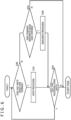
- BG Job namely the queues for management processing (the queues 64, 66, and 68 in the example illustrated in FIG. 3 ) are subject to processing. Any one of the commands stored in these queues includes the processing of moving the data already stored in the flash memory 20 to another region; in phase 3, these commands execute only a part of this processing, namely, the reading of the original data.
- the data that has been read is temporarily stored in an internal memory or the system memory 14.
- the write to the TLC and the data delete require a time that is several times longer. Therefore, the latter is summed up as phase 5 and, at the same time, a time limit is arranged, thereby enabling the transition to another phase by pausing the processing even if the processing is going on.
- the time limit of phase 5 is set to "3.0 msec.”
- the processing of phase 5 may be discontinued upon storing a command into a queue high in emergency, such as the queue 52 for emergency read illustrated in FIG. 3 , for example.
- the command processing block 46 checks again, every time one command is processed, whether or not commands are stored in the queue of the highest emergency queue and, if commands are stored, processes these commands (Y of S10, S12). If there is no command to be processed in the queue of the highest emergency (N of S10) and the number of commands processed so far is below the processing upper limit setting (Y of S14), then the commands stored in the queue of the next highest emergency are processed (Y of S16, S18). If there is not command to be processed in the queue concerned (N of S16), then it is checked whether or not commands are stored in the queue of the lowest emergency (the normal priority read queue 56 illustrated in FIG. 3 ) (S22).
- the command processing block 46 In a case where commands are stored (Y of S22), the command processing block 46 reads the command first stored in the queue concerned and then reads the data in the same manner as described above (S24). If the processing upper limit setting cannot be reached by the above-mentioned processing (Y of S20), the command processing block 46 checks again, every time one command is processed, whether or not commands are stored in the queue of the highest emergency queue and, if commands are stored, processes these commands (Y of S10, S12). If the number of times commands have been processing reaches the upper limit in any of these cycles (N of S14 or N of S20) or if there is no more command to be processed (N of S22), then this phase is terminated to transition to the next phase.
- the command processing block 46 reads the command first stored in the queue concerned and executes data read/write processing in the same manner as described above (S38).
- the processing upper limit is set to each of read processing and write processing, so that, every time one command is processed, the number of commands is compared with the upper limit for each of the contents of this processing. If the number of processing operations has not been reached (Y of S34), it is checked again whether or not commands are stored in the fast write queue and, if commands are stored, these commands are processed (Y of S30, S32).
- the processing is continued while checking whether commands are not stored in the read queue of the highest emergency for the NSIDb and the time limit set to phase 5 has not been reached (N of S56, N of S58, and N of S60). If either the storage of commands into the emergency queue or the expiration of the time limit occurs (Y of S56 or Y of S58), the started processing is discontinued, transitioning to the next phase (S62). In this case, the transition is made from phase 1 to phase 4 to phase 5 again, thereby restarting the discontinued processing.
- the number of processed commands is lower than the upper limit setting of the write processing (Y of S64)
- the started processing is discontinued, transitioning to the next phase (S62).
- the phase concerned is terminated, transitioning to the next phase (N of S64).
- the frequency of the occurrence of the management processing to be executed in phase 3 and phase 5 is influenced by the number of commands to be executed in phase 1, phase 2, and phase 4.
- the processing of copying the SLC to the TLC is executed on a three page basis. In a case where the write for one page to the SLC is executed every time in phase 2, copying from the SLC to the TLC once in three intervals can make ends meet. Therefore, the remaining 66% of time can be allocated to another management processing operation.
- the diagram illustrates, in rectangles from top to bottom, intervals in which frame n, frame n+1, frame n+2, ... are displayed on the display apparatus, intervals in which each frame is drawn, and each phase of the memory access by the flash controller 18.
- the dark interval in the display processing on top correspond to vertical blanking intervals.
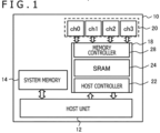
- the information processing apparatus mainly the host unit 12
- the drawing interval of each frame and the size and the frequency of request for the data to be read from the flash memory 20 are different.
- Each white arrow (an arrow 80, for example) downward from the rectangle of a drawing interval is illustrative of the issue timing of a read command from the host unit 12.
- the necessity of the adjustment may be determined by setting a threshold value to the number of commands actually stored in management processing queues by forecasting the number of stored commands from command storage situations so far.
- the command adjusting block 50 upon completion of the management processing targeted by the monitoring items, the command adjusting block 50 returns the switching rules to the original form and return the number of times commands have been issued to the normal state by notifying the host unit of the returning to the original switching rules.
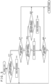
- two or more queues are sorted and an interval (phase) is arranged for each type in which processing is executed.
- This arrangement allows, for each individual queue, the double imposition of the switching rules for the queues to be processed in the same phase and the switching rules between the phases, thereby providing detailed settings by combining these switching rules and, eventually, the flexible operations fit to actual situations.
- the queues for such management processing as garbage collection, data copy for read disturb avoidance, and SLC-to-TLC data copy are likewise assembled into the above-mentioned system.
- This arrangement can prevent the congestion, due to the management processing, of the processing of access requests high in emergency from the host unit.
- setting the rules using absolute indexes for each queue, such as the upper limit of the number of times commands are processed and the time limit thereof can optimize the balance between the both, thereby executing the necessary processing with a low delay without failure.
- cycling the phases facilitates the estimate of processing intervals, thereby enabling bandwidth control.
- some of the management processing described above have unique characteristics of requiring lots of time once the necessity occurs although not frequent.
- the switching rules are temporarily changed or the issue of requests low in emergency by the host unit is held down.
- This arrangement can easily realize flexible measures such as temporarily increasing the time to be allocated to management processing for promotion, while assuring the minimum necessary access processing for the processing by the host unit.
- the present invention is applicable to an information processing apparatus and a memory controller that execute memory access processing.
Landscapes
- Engineering & Computer Science (AREA)
- Theoretical Computer Science (AREA)
- Physics & Mathematics (AREA)
- General Engineering & Computer Science (AREA)
- General Physics & Mathematics (AREA)
- Human Computer Interaction (AREA)
- Memory System (AREA)
- Information Retrieval, Db Structures And Fs Structures Therefor (AREA)
- Techniques For Improving Reliability Of Storages (AREA)
Applications Claiming Priority (2)
| Application Number | Priority Date | Filing Date | Title |
|---|---|---|---|
| JP2016247049A JP6677627B2 (ja) | 2016-12-20 | 2016-12-20 | 情報処理装置およびメモリアクセス方法 |
| PCT/JP2017/044777 WO2018116937A1 (ja) | 2016-12-20 | 2017-12-13 | 情報処理装置およびメモリアクセス方法 |
Publications (3)
| Publication Number | Publication Date |
|---|---|
| EP3561678A1 EP3561678A1 (en) | 2019-10-30 |
| EP3561678A4 EP3561678A4 (en) | 2020-08-05 |
| EP3561678B1 true EP3561678B1 (en) | 2023-05-17 |
Family
ID=62626406
Family Applications (1)
| Application Number | Title | Priority Date | Filing Date |
|---|---|---|---|
| EP17883337.2A Active EP3561678B1 (en) | 2016-12-20 | 2017-12-13 | Information processing device and memory access method |
Country Status (7)
| Country | Link |
|---|---|
| US (1) | US11281572B2 (zh) |
| EP (1) | EP3561678B1 (zh) |
| JP (1) | JP6677627B2 (zh) |
| KR (1) | KR102246840B1 (zh) |
| CN (1) | CN110073337B (zh) |
| TW (1) | TWI662418B (zh) |
| WO (1) | WO2018116937A1 (zh) |
Families Citing this family (8)
| Publication number | Priority date | Publication date | Assignee | Title |
|---|---|---|---|---|
| US11061822B2 (en) * | 2018-08-27 | 2021-07-13 | Qualcomm Incorporated | Method, apparatus, and system for reducing pipeline stalls due to address translation misses |
| CN111124254B (zh) * | 2018-10-30 | 2023-09-29 | 伊姆西Ip控股有限责任公司 | 调度存储空间回收请求的方法、电子设备和程序产品 |
| KR102686435B1 (ko) * | 2019-06-28 | 2024-07-19 | 에스케이하이닉스 주식회사 | 메모리 시스템, 메모리 컨트롤러 및 그 저장 방법 |
| CN110362275B (zh) * | 2019-07-10 | 2021-09-07 | 深圳大普微电子科技有限公司 | 提升固态硬盘服务质量的方法及固态硬盘 |
| US11029874B2 (en) * | 2019-07-30 | 2021-06-08 | Western Digital Technologies, Inc. | Rolling XOR protection in efficient pipeline |
| JP2021086583A (ja) * | 2019-11-29 | 2021-06-03 | キヤノン株式会社 | 情報処理装置、制御装置および制御装置の制御方法 |
| US20220004337A1 (en) * | 2020-07-06 | 2022-01-06 | Micron Technology, Inc. | Command prioritization in a command queue |
| CN114168495A (zh) * | 2020-09-10 | 2022-03-11 | 西部数据技术公司 | 存储设备的增强的预读能力 |
Family Cites Families (31)
| Publication number | Priority date | Publication date | Assignee | Title |
|---|---|---|---|---|
| US6570876B1 (en) * | 1998-04-01 | 2003-05-27 | Hitachi, Ltd. | Packet switch and switching method for switching variable length packets |
| JP2000285082A (ja) | 1999-03-31 | 2000-10-13 | Toshiba Corp | 中央演算装置及びコンパイル方法 |
| JP4327081B2 (ja) * | 2004-12-28 | 2009-09-09 | 京セラミタ株式会社 | メモリアクセス制御回路 |
| US20060184718A1 (en) * | 2005-02-16 | 2006-08-17 | Sinclair Alan W | Direct file data programming and deletion in flash memories |
| JP4419868B2 (ja) | 2005-02-25 | 2010-02-24 | ソニー株式会社 | 情報処理装置および方法、メモリ制御装置および方法、記録媒体、並びにプログラム |
| JP4142068B2 (ja) * | 2006-06-16 | 2008-08-27 | 株式会社ソニー・コンピュータエンタテインメント | 情報処理装置およびアクセス制御方法 |
| US8208406B1 (en) * | 2008-03-25 | 2012-06-26 | Juniper Networks, Inc. | Packet forwarding using feedback controlled weighted queues dynamically adjusted based on processor utilization |
| JP5147584B2 (ja) * | 2008-07-23 | 2013-02-20 | 株式会社日立製作所 | ストレージサブシステム及びコントローラによるコマンド実行方法 |
| JP2010176646A (ja) * | 2009-02-02 | 2010-08-12 | Toshiba Information Systems (Japan) Corp | メモリシステムおよびメモリシステムのインターリーブ制御方法 |
| CN101498994B (zh) * | 2009-02-16 | 2011-04-20 | 华中科技大学 | 一种固态硬盘控制器 |
| US8688894B2 (en) * | 2009-09-03 | 2014-04-01 | Pioneer Chip Technology Ltd. | Page based management of flash storage |
| US8595411B2 (en) * | 2009-12-30 | 2013-11-26 | Sandisk Technologies Inc. | Method and controller for performing a sequence of commands |
| US8838853B2 (en) * | 2010-01-18 | 2014-09-16 | Marvell International Ltd. | Access buffer |
| US8468318B2 (en) | 2010-09-15 | 2013-06-18 | Pure Storage Inc. | Scheduling of I/O writes in a storage environment |
| US8271692B1 (en) * | 2010-10-01 | 2012-09-18 | Western Digital Technologies, Inc. | Throttled command completion time |
| US20120246385A1 (en) * | 2011-03-22 | 2012-09-27 | American Megatrends, Inc. | Emulating spi or 12c prom/eprom/eeprom using flash memory of microcontroller |
| US8700834B2 (en) * | 2011-09-06 | 2014-04-15 | Western Digital Technologies, Inc. | Systems and methods for an enhanced controller architecture in data storage systems |
| JP2013200692A (ja) * | 2012-03-23 | 2013-10-03 | Toshiba Corp | メモリシステム |
| US8996782B2 (en) * | 2012-03-23 | 2015-03-31 | Kabushiki Kaisha Toshiba | Memory system and bank interleaving method |
| US9058208B2 (en) | 2012-11-12 | 2015-06-16 | Skymedi Corporation | Method of scheduling tasks for memories and memory system thereof |
| CN103488578B (zh) * | 2012-12-28 | 2016-05-25 | 晶天电子(深圳)有限公司 | 虚拟存储设备(vmd)应用/驱动器 |
| US8959263B2 (en) * | 2013-01-08 | 2015-02-17 | Apple Inc. | Maintaining I/O priority and I/O sorting |
| WO2014132346A1 (ja) | 2013-02-27 | 2014-09-04 | 株式会社日立製作所 | 半導体ストレージ |
| US9268495B2 (en) * | 2013-03-15 | 2016-02-23 | Apple Inc. | Managing I/O priorities |
| WO2015145552A1 (ja) * | 2014-03-24 | 2015-10-01 | 株式会社日立製作所 | 不揮発メモリデバイス、及び、不揮発メモリデバイスを有するストレージ装置 |
| US10073714B2 (en) | 2015-03-11 | 2018-09-11 | Western Digital Technologies, Inc. | Task queues |
| TWI588652B (zh) * | 2015-09-01 | 2017-06-21 | 慧榮科技股份有限公司 | 讀取及寫入命令排程方法以及使用該方法的裝置 |
| US10866910B2 (en) * | 2015-09-28 | 2020-12-15 | Sandisk Technologies Llc | Systems, methods, and computer-readable media for managing instruction fetch in virtual computing environments |
| US9910772B2 (en) * | 2016-04-27 | 2018-03-06 | Silicon Motion Inc. | Flash memory apparatus and storage management method for flash memory |
| JP6783645B2 (ja) * | 2016-12-21 | 2020-11-11 | キオクシア株式会社 | メモリシステムおよび制御方法 |
| US10831403B2 (en) * | 2017-05-19 | 2020-11-10 | Seagate Technology Llc | Probabalistic command aging and selection |
-
2016
- 2016-12-20 JP JP2016247049A patent/JP6677627B2/ja active Active
-
2017
- 2017-10-26 TW TW106136823A patent/TWI662418B/zh active
- 2017-12-13 CN CN201780077153.8A patent/CN110073337B/zh active Active
- 2017-12-13 EP EP17883337.2A patent/EP3561678B1/en active Active
- 2017-12-13 US US16/346,717 patent/US11281572B2/en active Active
- 2017-12-13 KR KR1020197016557A patent/KR102246840B1/ko active IP Right Grant
- 2017-12-13 WO PCT/JP2017/044777 patent/WO2018116937A1/ja unknown
Also Published As
| Publication number | Publication date |
|---|---|
| EP3561678A1 (en) | 2019-10-30 |
| US20200073793A1 (en) | 2020-03-05 |
| WO2018116937A1 (ja) | 2018-06-28 |
| CN110073337A (zh) | 2019-07-30 |
| JP2018101301A (ja) | 2018-06-28 |
| EP3561678A4 (en) | 2020-08-05 |
| CN110073337B (zh) | 2023-06-02 |
| TW201824010A (zh) | 2018-07-01 |
| KR102246840B1 (ko) | 2021-04-30 |
| TWI662418B (zh) | 2019-06-11 |
| US11281572B2 (en) | 2022-03-22 |
| JP6677627B2 (ja) | 2020-04-08 |
| KR20190079672A (ko) | 2019-07-05 |
Similar Documents
| Publication | Publication Date | Title |
|---|---|---|
| EP3561678B1 (en) | Information processing device and memory access method | |
| US9244617B2 (en) | Scheduling requests in a solid state memory device | |
| US11704239B2 (en) | Garbage collection method for storage medium, storage medium, and program product | |
| US9635123B2 (en) | Computer system, and arrangement of data control method | |
| US20230042833A1 (en) | Multistreaming in heterogeneous environments | |
| JP7443195B2 (ja) | メモリシステムおよび制御方法 | |
| US10817186B2 (en) | Memory system | |
| US20170003911A1 (en) | Information processing device | |
| CN110908595B (zh) | 存储装置及信息处理系统 | |
| CN115576876A (zh) | 一种应用于NVMe SSD的DMA分配与管理方法 | |
| US11402999B2 (en) | Adaptive wear leveling using multiple partitions | |
| US9058113B2 (en) | Storage region providing device, storage region providing method, and recording medium | |
| KR20180133730A (ko) | 스토리지 시스템 및 이의 동작 방법 | |
| US20130332661A1 (en) | Information processing apparatus and method and program | |
| JP2006039942A (ja) | 階層記憶システムにおけるファイル管理装置及びそのファイル管理方法 | |
| US11630776B2 (en) | Methods and systems for fast allocation of fragmented caches | |
| KR102334237B1 (ko) | 다중 포그라운드 어플리케이션을 위한 페이지 캐쉬 관리 방법 및 장치 | |
| US20220283705A1 (en) | Storage management apparatus, storage management method, and program | |
| US20230244383A1 (en) | Memory system and method of controlling nonvolatile memory | |
| JP2017134446A (ja) | メモリ制御装置、記憶装置、メモリ制御方法およびコンピュータプログラム | |
| JP2001306263A (ja) | メディアデータ記憶装置 |
Legal Events
| Date | Code | Title | Description |
|---|---|---|---|
| STAA | Information on the status of an ep patent application or granted ep patent |
Free format text: STATUS: THE INTERNATIONAL PUBLICATION HAS BEEN MADE |
|
| PUAI | Public reference made under article 153(3) epc to a published international application that has entered the european phase |
Free format text: ORIGINAL CODE: 0009012 |
|
| STAA | Information on the status of an ep patent application or granted ep patent |
Free format text: STATUS: REQUEST FOR EXAMINATION WAS MADE |
|
| 17P | Request for examination filed |
Effective date: 20190617 |
|
| AK | Designated contracting states |
Kind code of ref document: A1 Designated state(s): AL AT BE BG CH CY CZ DE DK EE ES FI FR GB GR HR HU IE IS IT LI LT LU LV MC MK MT NL NO PL PT RO RS SE SI SK SM TR |
|
| AX | Request for extension of the european patent |
Extension state: BA ME |
|
| DAV | Request for validation of the european patent (deleted) | ||
| DAX | Request for extension of the european patent (deleted) | ||
| A4 | Supplementary search report drawn up and despatched |
Effective date: 20200703 |
|
| RIC1 | Information provided on ipc code assigned before grant |
Ipc: G06F 12/00 20060101AFI20200629BHEP Ipc: G06F 12/02 20060101ALI20200629BHEP Ipc: G06F 13/16 20060101ALI20200629BHEP Ipc: G06F 3/06 20060101ALI20200629BHEP |
|
| STAA | Information on the status of an ep patent application or granted ep patent |
Free format text: STATUS: EXAMINATION IS IN PROGRESS |
|
| 17Q | First examination report despatched |
Effective date: 20210615 |
|
| STAA | Information on the status of an ep patent application or granted ep patent |
Free format text: STATUS: EXAMINATION IS IN PROGRESS |
|
| GRAP | Despatch of communication of intention to grant a patent |
Free format text: ORIGINAL CODE: EPIDOSNIGR1 |
|
| STAA | Information on the status of an ep patent application or granted ep patent |
Free format text: STATUS: GRANT OF PATENT IS INTENDED |
|
| INTG | Intention to grant announced |
Effective date: 20221215 |
|
| GRAS | Grant fee paid |
Free format text: ORIGINAL CODE: EPIDOSNIGR3 |
|
| GRAA | (expected) grant |
Free format text: ORIGINAL CODE: 0009210 |
|
| STAA | Information on the status of an ep patent application or granted ep patent |
Free format text: STATUS: THE PATENT HAS BEEN GRANTED |
|
| AK | Designated contracting states |
Kind code of ref document: B1 Designated state(s): AL AT BE BG CH CY CZ DE DK EE ES FI FR GB GR HR HU IE IS IT LI LT LU LV MC MK MT NL NO PL PT RO RS SE SI SK SM TR |
|
| REG | Reference to a national code |
Ref country code: GB Ref legal event code: FG4D |
|
| REG | Reference to a national code |
Ref country code: CH Ref legal event code: EP |
|
| REG | Reference to a national code |
Ref country code: DE Ref legal event code: R096 Ref document number: 602017068907 Country of ref document: DE |
|
| REG | Reference to a national code |
Ref country code: IE Ref legal event code: FG4D |
|
| REG | Reference to a national code |
Ref country code: AT Ref legal event code: REF Ref document number: 1568684 Country of ref document: AT Kind code of ref document: T Effective date: 20230615 |
|
| P01 | Opt-out of the competence of the unified patent court (upc) registered |
Effective date: 20230623 |
|
| REG | Reference to a national code |
Ref country code: LT Ref legal event code: MG9D |
|
| REG | Reference to a national code |
Ref country code: NL Ref legal event code: MP Effective date: 20230517 |
|
| REG | Reference to a national code |
Ref country code: AT Ref legal event code: MK05 Ref document number: 1568684 Country of ref document: AT Kind code of ref document: T Effective date: 20230517 |
|
| PG25 | Lapsed in a contracting state [announced via postgrant information from national office to epo] |
Ref country code: SE Free format text: LAPSE BECAUSE OF FAILURE TO SUBMIT A TRANSLATION OF THE DESCRIPTION OR TO PAY THE FEE WITHIN THE PRESCRIBED TIME-LIMIT Effective date: 20230517 Ref country code: PT Free format text: LAPSE BECAUSE OF FAILURE TO SUBMIT A TRANSLATION OF THE DESCRIPTION OR TO PAY THE FEE WITHIN THE PRESCRIBED TIME-LIMIT Effective date: 20230918 Ref country code: NO Free format text: LAPSE BECAUSE OF FAILURE TO SUBMIT A TRANSLATION OF THE DESCRIPTION OR TO PAY THE FEE WITHIN THE PRESCRIBED TIME-LIMIT Effective date: 20230817 Ref country code: NL Free format text: LAPSE BECAUSE OF FAILURE TO SUBMIT A TRANSLATION OF THE DESCRIPTION OR TO PAY THE FEE WITHIN THE PRESCRIBED TIME-LIMIT Effective date: 20230517 Ref country code: ES Free format text: LAPSE BECAUSE OF FAILURE TO SUBMIT A TRANSLATION OF THE DESCRIPTION OR TO PAY THE FEE WITHIN THE PRESCRIBED TIME-LIMIT Effective date: 20230517 Ref country code: AT Free format text: LAPSE BECAUSE OF FAILURE TO SUBMIT A TRANSLATION OF THE DESCRIPTION OR TO PAY THE FEE WITHIN THE PRESCRIBED TIME-LIMIT Effective date: 20230517 |
|
| PG25 | Lapsed in a contracting state [announced via postgrant information from national office to epo] |
Ref country code: RS Free format text: LAPSE BECAUSE OF FAILURE TO SUBMIT A TRANSLATION OF THE DESCRIPTION OR TO PAY THE FEE WITHIN THE PRESCRIBED TIME-LIMIT Effective date: 20230517 Ref country code: PL Free format text: LAPSE BECAUSE OF FAILURE TO SUBMIT A TRANSLATION OF THE DESCRIPTION OR TO PAY THE FEE WITHIN THE PRESCRIBED TIME-LIMIT Effective date: 20230517 Ref country code: LV Free format text: LAPSE BECAUSE OF FAILURE TO SUBMIT A TRANSLATION OF THE DESCRIPTION OR TO PAY THE FEE WITHIN THE PRESCRIBED TIME-LIMIT Effective date: 20230517 Ref country code: LT Free format text: LAPSE BECAUSE OF FAILURE TO SUBMIT A TRANSLATION OF THE DESCRIPTION OR TO PAY THE FEE WITHIN THE PRESCRIBED TIME-LIMIT Effective date: 20230517 Ref country code: IS Free format text: LAPSE BECAUSE OF FAILURE TO SUBMIT A TRANSLATION OF THE DESCRIPTION OR TO PAY THE FEE WITHIN THE PRESCRIBED TIME-LIMIT Effective date: 20230917 Ref country code: HR Free format text: LAPSE BECAUSE OF FAILURE TO SUBMIT A TRANSLATION OF THE DESCRIPTION OR TO PAY THE FEE WITHIN THE PRESCRIBED TIME-LIMIT Effective date: 20230517 Ref country code: GR Free format text: LAPSE BECAUSE OF FAILURE TO SUBMIT A TRANSLATION OF THE DESCRIPTION OR TO PAY THE FEE WITHIN THE PRESCRIBED TIME-LIMIT Effective date: 20230818 |
|
| PG25 | Lapsed in a contracting state [announced via postgrant information from national office to epo] |
Ref country code: FI Free format text: LAPSE BECAUSE OF FAILURE TO SUBMIT A TRANSLATION OF THE DESCRIPTION OR TO PAY THE FEE WITHIN THE PRESCRIBED TIME-LIMIT Effective date: 20230517 |
|
| PG25 | Lapsed in a contracting state [announced via postgrant information from national office to epo] |
Ref country code: SK Free format text: LAPSE BECAUSE OF FAILURE TO SUBMIT A TRANSLATION OF THE DESCRIPTION OR TO PAY THE FEE WITHIN THE PRESCRIBED TIME-LIMIT Effective date: 20230517 |
|
| PGFP | Annual fee paid to national office [announced via postgrant information from national office to epo] |
Ref country code: GB Payment date: 20231124 Year of fee payment: 7 |
|
| PG25 | Lapsed in a contracting state [announced via postgrant information from national office to epo] |
Ref country code: SM Free format text: LAPSE BECAUSE OF FAILURE TO SUBMIT A TRANSLATION OF THE DESCRIPTION OR TO PAY THE FEE WITHIN THE PRESCRIBED TIME-LIMIT Effective date: 20230517 Ref country code: SK Free format text: LAPSE BECAUSE OF FAILURE TO SUBMIT A TRANSLATION OF THE DESCRIPTION OR TO PAY THE FEE WITHIN THE PRESCRIBED TIME-LIMIT Effective date: 20230517 Ref country code: RO Free format text: LAPSE BECAUSE OF FAILURE TO SUBMIT A TRANSLATION OF THE DESCRIPTION OR TO PAY THE FEE WITHIN THE PRESCRIBED TIME-LIMIT Effective date: 20230517 Ref country code: EE Free format text: LAPSE BECAUSE OF FAILURE TO SUBMIT A TRANSLATION OF THE DESCRIPTION OR TO PAY THE FEE WITHIN THE PRESCRIBED TIME-LIMIT Effective date: 20230517 Ref country code: DK Free format text: LAPSE BECAUSE OF FAILURE TO SUBMIT A TRANSLATION OF THE DESCRIPTION OR TO PAY THE FEE WITHIN THE PRESCRIBED TIME-LIMIT Effective date: 20230517 Ref country code: CZ Free format text: LAPSE BECAUSE OF FAILURE TO SUBMIT A TRANSLATION OF THE DESCRIPTION OR TO PAY THE FEE WITHIN THE PRESCRIBED TIME-LIMIT Effective date: 20230517 |
|
| PGFP | Annual fee paid to national office [announced via postgrant information from national office to epo] |
Ref country code: FR Payment date: 20231122 Year of fee payment: 7 Ref country code: DE Payment date: 20231121 Year of fee payment: 7 |
|
| REG | Reference to a national code |
Ref country code: DE Ref legal event code: R097 Ref document number: 602017068907 Country of ref document: DE |
|
| PLBE | No opposition filed within time limit |
Free format text: ORIGINAL CODE: 0009261 |
|
| STAA | Information on the status of an ep patent application or granted ep patent |
Free format text: STATUS: NO OPPOSITION FILED WITHIN TIME LIMIT |
|
| 26N | No opposition filed |
Effective date: 20240220 |
|
| PG25 | Lapsed in a contracting state [announced via postgrant information from national office to epo] |
Ref country code: SI Free format text: LAPSE BECAUSE OF FAILURE TO SUBMIT A TRANSLATION OF THE DESCRIPTION OR TO PAY THE FEE WITHIN THE PRESCRIBED TIME-LIMIT Effective date: 20230517 |
|
| PG25 | Lapsed in a contracting state [announced via postgrant information from national office to epo] |
Ref country code: SI Free format text: LAPSE BECAUSE OF FAILURE TO SUBMIT A TRANSLATION OF THE DESCRIPTION OR TO PAY THE FEE WITHIN THE PRESCRIBED TIME-LIMIT Effective date: 20230517 Ref country code: IT Free format text: LAPSE BECAUSE OF FAILURE TO SUBMIT A TRANSLATION OF THE DESCRIPTION OR TO PAY THE FEE WITHIN THE PRESCRIBED TIME-LIMIT Effective date: 20230517 |
|
| REG | Reference to a national code |
Ref country code: CH Ref legal event code: PL |
|
| PG25 | Lapsed in a contracting state [announced via postgrant information from national office to epo] |
Ref country code: LU Free format text: LAPSE BECAUSE OF NON-PAYMENT OF DUE FEES Effective date: 20231213 |
|
| PG25 | Lapsed in a contracting state [announced via postgrant information from national office to epo] |
Ref country code: MC Free format text: LAPSE BECAUSE OF FAILURE TO SUBMIT A TRANSLATION OF THE DESCRIPTION OR TO PAY THE FEE WITHIN THE PRESCRIBED TIME-LIMIT Effective date: 20230517 |
|
| REG | Reference to a national code |
Ref country code: BE Ref legal event code: MM Effective date: 20231231 |
|
| PG25 | Lapsed in a contracting state [announced via postgrant information from national office to epo] |
Ref country code: MC Free format text: LAPSE BECAUSE OF FAILURE TO SUBMIT A TRANSLATION OF THE DESCRIPTION OR TO PAY THE FEE WITHIN THE PRESCRIBED TIME-LIMIT Effective date: 20230517 Ref country code: LU Free format text: LAPSE BECAUSE OF NON-PAYMENT OF DUE FEES Effective date: 20231213 |