WO2018116602A1 - 弾性波装置、高周波フロントエンド回路及び通信装置 - Google Patents
弾性波装置、高周波フロントエンド回路及び通信装置 Download PDFInfo
- Publication number
- WO2018116602A1 WO2018116602A1 PCT/JP2017/037558 JP2017037558W WO2018116602A1 WO 2018116602 A1 WO2018116602 A1 WO 2018116602A1 JP 2017037558 W JP2017037558 W JP 2017037558W WO 2018116602 A1 WO2018116602 A1 WO 2018116602A1
- Authority
- WO
- WIPO (PCT)
- Prior art keywords
- elastic wave
- resonator
- idt electrode
- thickness
- electrode
- Prior art date
- Legal status (The legal status is an assumption and is not a legal conclusion. Google has not performed a legal analysis and makes no representation as to the accuracy of the status listed.)
- Ceased
Links
Images










Classifications
-
- H—ELECTRICITY
- H03—ELECTRONIC CIRCUITRY
- H03H—IMPEDANCE NETWORKS, e.g. RESONANT CIRCUITS; RESONATORS
- H03H9/00—Networks comprising electromechanical or electro-acoustic elements; Electromechanical resonators
- H03H9/02—Details
- H03H9/125—Driving means, e.g. electrodes, coils
- H03H9/145—Driving means, e.g. electrodes, coils for networks using surface acoustic waves
-
- H—ELECTRICITY
- H03—ELECTRONIC CIRCUITRY
- H03H—IMPEDANCE NETWORKS, e.g. RESONANT CIRCUITS; RESONATORS
- H03H9/00—Networks comprising electromechanical or electro-acoustic elements; Electromechanical resonators
- H03H9/02—Details
- H03H9/02535—Details of surface acoustic wave devices
- H03H9/02543—Characteristics of substrate, e.g. cutting angles
- H03H9/02559—Characteristics of substrate, e.g. cutting angles of lithium niobate or lithium-tantalate substrates
-
- H—ELECTRICITY
- H03—ELECTRONIC CIRCUITRY
- H03H—IMPEDANCE NETWORKS, e.g. RESONANT CIRCUITS; RESONATORS
- H03H9/00—Networks comprising electromechanical or electro-acoustic elements; Electromechanical resonators
- H03H9/02—Details
- H03H9/02535—Details of surface acoustic wave devices
- H03H9/02818—Means for compensation or elimination of undesirable effects
- H03H9/02834—Means for compensation or elimination of undesirable effects of temperature influence
-
- H—ELECTRICITY
- H03—ELECTRONIC CIRCUITRY
- H03H—IMPEDANCE NETWORKS, e.g. RESONANT CIRCUITS; RESONATORS
- H03H9/00—Networks comprising electromechanical or electro-acoustic elements; Electromechanical resonators
- H03H9/02—Details
- H03H9/125—Driving means, e.g. electrodes, coils
- H03H9/145—Driving means, e.g. electrodes, coils for networks using surface acoustic waves
- H03H9/14538—Formation
-
- H—ELECTRICITY
- H03—ELECTRONIC CIRCUITRY
- H03H—IMPEDANCE NETWORKS, e.g. RESONANT CIRCUITS; RESONATORS
- H03H9/00—Networks comprising electromechanical or electro-acoustic elements; Electromechanical resonators
- H03H9/02—Details
- H03H9/125—Driving means, e.g. electrodes, coils
- H03H9/145—Driving means, e.g. electrodes, coils for networks using surface acoustic waves
- H03H9/14538—Formation
- H03H9/14541—Multilayer finger or busbar electrode
-
- H—ELECTRICITY
- H03—ELECTRONIC CIRCUITRY
- H03H—IMPEDANCE NETWORKS, e.g. RESONANT CIRCUITS; RESONATORS
- H03H9/00—Networks comprising electromechanical or electro-acoustic elements; Electromechanical resonators
- H03H9/25—Constructional features of resonators using surface acoustic waves
-
- H—ELECTRICITY
- H03—ELECTRONIC CIRCUITRY
- H03H—IMPEDANCE NETWORKS, e.g. RESONANT CIRCUITS; RESONATORS
- H03H9/00—Networks comprising electromechanical or electro-acoustic elements; Electromechanical resonators
- H03H9/46—Filters
- H03H9/64—Filters using surface acoustic waves
-
- H—ELECTRICITY
- H03—ELECTRONIC CIRCUITRY
- H03H—IMPEDANCE NETWORKS, e.g. RESONANT CIRCUITS; RESONATORS
- H03H9/00—Networks comprising electromechanical or electro-acoustic elements; Electromechanical resonators
- H03H9/46—Filters
- H03H9/64—Filters using surface acoustic waves
- H03H9/6423—Means for obtaining a particular transfer characteristic
- H03H9/6433—Coupled resonator filters
- H03H9/6483—Ladder SAW filters
-
- H—ELECTRICITY
- H03—ELECTRONIC CIRCUITRY
- H03H—IMPEDANCE NETWORKS, e.g. RESONANT CIRCUITS; RESONATORS
- H03H9/00—Networks comprising electromechanical or electro-acoustic elements; Electromechanical resonators
- H03H9/46—Filters
- H03H9/64—Filters using surface acoustic waves
- H03H9/6489—Compensation of undesirable effects
- H03H9/6496—Reducing ripple in transfer characteristic
-
- H—ELECTRICITY
- H03—ELECTRONIC CIRCUITRY
- H03H—IMPEDANCE NETWORKS, e.g. RESONANT CIRCUITS; RESONATORS
- H03H9/00—Networks comprising electromechanical or electro-acoustic elements; Electromechanical resonators
- H03H9/70—Multiple-port networks for connecting several sources or loads, working on different frequencies or frequency bands, to a common load or source
- H03H9/72—Networks using surface acoustic waves
-
- H—ELECTRICITY
- H03—ELECTRONIC CIRCUITRY
- H03H—IMPEDANCE NETWORKS, e.g. RESONANT CIRCUITS; RESONATORS
- H03H9/00—Networks comprising electromechanical or electro-acoustic elements; Electromechanical resonators
- H03H9/70—Multiple-port networks for connecting several sources or loads, working on different frequencies or frequency bands, to a common load or source
- H03H9/72—Networks using surface acoustic waves
- H03H9/725—Duplexers
-
- H—ELECTRICITY
- H04—ELECTRIC COMMUNICATION TECHNIQUE
- H04B—TRANSMISSION
- H04B1/00—Details of transmission systems, not covered by a single one of groups H04B3/00 - H04B13/00; Details of transmission systems not characterised by the medium used for transmission
- H04B1/005—Details of transmission systems, not covered by a single one of groups H04B3/00 - H04B13/00; Details of transmission systems not characterised by the medium used for transmission adapting radio receivers, transmitters andtransceivers for operation on two or more bands, i.e. frequency ranges
- H04B1/0053—Details of transmission systems, not covered by a single one of groups H04B3/00 - H04B13/00; Details of transmission systems not characterised by the medium used for transmission adapting radio receivers, transmitters andtransceivers for operation on two or more bands, i.e. frequency ranges with common antenna for more than one band
- H04B1/0057—Details of transmission systems, not covered by a single one of groups H04B3/00 - H04B13/00; Details of transmission systems not characterised by the medium used for transmission adapting radio receivers, transmitters andtransceivers for operation on two or more bands, i.e. frequency ranges with common antenna for more than one band using diplexing or multiplexing filters for selecting the desired band
-
- H—ELECTRICITY
- H04—ELECTRIC COMMUNICATION TECHNIQUE
- H04B—TRANSMISSION
- H04B1/00—Details of transmission systems, not covered by a single one of groups H04B3/00 - H04B13/00; Details of transmission systems not characterised by the medium used for transmission
- H04B1/02—Transmitters
- H04B1/04—Circuits
- H04B1/0475—Circuits with means for limiting noise, interference or distortion
-
- H—ELECTRICITY
- H04—ELECTRIC COMMUNICATION TECHNIQUE
- H04B—TRANSMISSION
- H04B1/00—Details of transmission systems, not covered by a single one of groups H04B3/00 - H04B13/00; Details of transmission systems not characterised by the medium used for transmission
- H04B1/38—Transceivers, i.e. devices in which transmitter and receiver form a structural unit and in which at least one part is used for functions of transmitting and receiving
- H04B1/40—Circuits
- H04B1/50—Circuits using different frequencies for the two directions of communication
-
- H—ELECTRICITY
- H04—ELECTRIC COMMUNICATION TECHNIQUE
- H04B—TRANSMISSION
- H04B1/00—Details of transmission systems, not covered by a single one of groups H04B3/00 - H04B13/00; Details of transmission systems not characterised by the medium used for transmission
- H04B1/02—Transmitters
- H04B1/04—Circuits
- H04B2001/0408—Circuits with power amplifiers
Definitions
- the present invention relates to an elastic wave device using a Rayleigh wave, a high-frequency front-end circuit and a communication device using the elastic wave device.
- Patent Documents 1 and 2 disclose elastic wave devices using Rayleigh waves.
- the elastic wave device of Patent Document 1 includes a series arm resonator and a parallel arm resonator made of an elastic wave resonator.
- the thickness of the silicon oxide film constituting the acoustic wave resonator differs between the series arm resonator and the parallel arm resonator.
- the elastic wave propagation direction differs between the elastic wave resonator constituting the series arm resonator and the elastic wave resonator constituting the parallel arm resonator. Yes.
- the elastic wave device of Patent Document 2 below includes a LiNbO 3 substrate and an electrode including an IDT electrode mainly composed of Au.
- Patent Document 2 describes that ⁇ at the Euler angles ( ⁇ , ⁇ , ⁇ ) of the LiNbO 3 substrate and the thickness of the electrode have a specific relationship.
- spurious vibrations different from the spurious waves to be suppressed may occur in the pass band or in the vicinity of the pass band. there were.
- Patent Document 2 since the specific relationship between the Euler angle ⁇ and the thickness of the electrode is in a wide range, spurious due to SH waves is generated when the thicknesses of silicon oxides are different in a plurality of acoustic wave resonators. There was a possibility that.
- An object of the present invention is to make it possible to suppress spurious due to SH waves while achieving downsizing, and to further provide an acoustic wave device having a steep filter characteristic and a wide passband, and a high-frequency front using the acoustic wave device.
- An end circuit and a communication device are provided.
- the acoustic wave device includes a LiNbO 3 substrate, a first IDT electrode provided on the LiNbO 3 substrate, and a first dielectric film provided so as to cover the first IDT electrode.
- a second acoustic wave resonator using a Rayleigh wave, wherein the thickness of the first dielectric film is different from the thickness of the second dielectric film,
- the propagation direction of the elastic wave in the elastic wave resonator matches the propagation direction of the elastic wave in the second elastic wave resonator, and the Euler angles ( ⁇ , ⁇ , ⁇ ) of the LiNbO 3 substrate are (0 ° ⁇ 5 °, ⁇ , 0 ° ⁇ 10 °), and the first IDT electrode and
- the second IDT electrode has a main electrode, and the thickness of the main electrode is normalized by a wavelength ⁇ determined by the electrode finger pitch of at least one of the first IDT electrode and the second IDT electrode.
- the density ratio between the density of the main electrode ([rho) and Pt density of ([rho Pt) to ( ⁇ / ⁇ Pt) is taken as r
- the Euler angles of the LiNbO 3 substrate ( ⁇ , ⁇ , ⁇ ) ⁇ satisfies the following formula (1) in the range of 0.055 ⁇ ⁇ T ⁇ r ⁇ 0.10 ⁇ .
- the first IDT electrode and the second IDT electrode are configured with the same electrode material and the same thickness.
- ⁇ at the Euler angles ( ⁇ , ⁇ , ⁇ ) of the LiNbO 3 substrate is in the range of ⁇ 2 ° to 2 °. In this case, it is possible to suppress spuriousness different from the spurious due to the SH wave.
- the first dielectric film and the second dielectric film each contain silicon oxide as a main component.
- the frequency temperature characteristic can be further improved.
- the first elastic wave resonator is a series arm resonator
- the second elastic wave resonator is a parallel arm resonator
- a ladder filter is formed by at least the first elastic wave resonator and the second elastic wave resonator.
- the elastic wave device includes: a transmission filter having the first elastic wave resonator; and a reception filter having the second elastic wave resonator. It is a duplexer.
- the high-frequency front-end circuit according to the present invention includes an elastic wave device configured according to the present invention and a power amplifier.
- the communication device includes a high-frequency front-end circuit configured according to the present invention and an RF signal processing circuit.
- an elastic wave device having a steep filter characteristic and a wide passband, a high-frequency front-end circuit, and a communication device Can be provided.
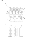
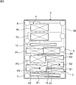
- FIG. 1 is a schematic plan view of an acoustic wave device according to an embodiment of the present invention.
- FIG. 2A is a circuit diagram of an elastic wave device according to an embodiment of the present invention
- FIG. 2B is a schematic plan view showing an electrode structure of a 1-port type elastic wave resonator.
- FIG. 3 is a schematic cross-sectional view showing a first elastic wave resonator constituting a series arm resonator in the elastic wave device according to the embodiment of the present invention.
- FIG. 4 is a schematic cross-sectional view showing a second elastic wave resonator constituting a parallel arm resonator in the elastic wave device according to the embodiment of the present invention.
- FIG. 1 is a schematic plan view of an acoustic wave device according to an embodiment of the present invention.
- FIG. 2A is a circuit diagram of an elastic wave device according to an embodiment of the present invention
- FIG. 2B is a schematic plan view showing an electrode structure of a 1-port type elastic wave
- FIG. 5 is a schematic plan view when the propagation direction of the elastic wave in the second elastic wave resonator is tilted by 1 ° with respect to the propagation direction of the elastic wave in the first elastic wave resonator.
- FIG. 6 is a schematic plan view when the propagation direction of the elastic wave in the second elastic wave resonator is inclined by 2 ° with respect to the propagation direction of the elastic wave in the first elastic wave resonator.
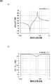
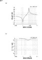
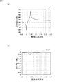
- FIG. 7A is a diagram showing the impedance characteristics when the thickness of the SiO 2 film is 0.2 ⁇
- FIG. 7B is a diagram showing the return loss characteristics.
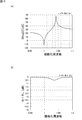
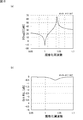
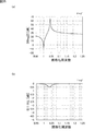
- FIG. 8A is a diagram showing impedance characteristics when the thickness of the SiO 2 film is 0.3 ⁇ , and FIG.
- FIG. 8B is a diagram showing return loss characteristics thereof.
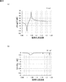
- FIG. 9A is a diagram showing the impedance characteristics when the thickness of the SiO 2 film is 0.4 ⁇
- FIG. 9B is a diagram showing the return loss characteristics.
- FIG. 10A is a diagram showing the impedance characteristics when the thickness of the SiO 2 film is 0.5 ⁇
- FIG. 10B is a diagram showing the return loss characteristics.
- FIG. 11A shows the impedance characteristics when the thickness of the SiO 2 film is 0.6 ⁇
- FIG. 11B shows the return loss characteristics.
- FIG. 12A is a diagram showing the impedance characteristics when Euler angle ⁇ is 27.5 °
- FIG. 12B is a diagram showing the return loss characteristics.
- FIG. 13A is a diagram showing impedance characteristics when Euler angle ⁇ is 28.0 °
- FIG. 13B is a diagram showing return loss characteristics thereof.
- FIG. 14A is a diagram showing impedance characteristics when Euler angle ⁇ is 28.5 °
- FIG. 14B is a diagram showing return loss characteristics thereof.
- FIG. 15A is a diagram showing impedance characteristics when Euler angle ⁇ is 29.0 °
- FIG. 15B is a diagram showing return loss characteristics thereof.
- FIG. 16A is a diagram showing impedance characteristics when Euler angle ⁇ is 29.5 °
- FIG. 16B is a diagram showing return loss characteristics thereof.
- FIG. 17A is a diagram showing impedance characteristics when Euler angle ⁇ is 30.0 °
- FIG. 17B is a diagram showing return loss characteristics thereof.
- FIG. 18A is a diagram showing the impedance characteristic when Euler angle ⁇ is 30.5 °
- FIG. 18B is a diagram showing the return loss characteristic.
- FIG. 19A is a diagram showing impedance characteristics when Euler angle ⁇ is 31.0 °
- FIG. 19B is a diagram showing return loss characteristics thereof.
- FIG. 20A is a diagram showing impedance characteristics when Euler angle ⁇ is 31.5 °
- FIG. 20B is a diagram showing return loss characteristics thereof.
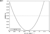
- FIG. 21 is a diagram illustrating the relationship between Euler angle ⁇ and the ratio band of the SH wave.
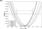
- FIG. 22 is a diagram showing the relationship between the Euler angle ⁇ and the SH wave ratio band when the thickness of the SiO 2 film is changed.
- FIG. 23 is a diagram showing the relationship between the Euler angle ⁇ and the thickness of the Pt film.
- FIG. 24A is a diagram showing the impedance characteristics when Euler angle ⁇ is 0 °
- FIG. 24B is a diagram showing the return loss characteristics.
- FIG. 25A is a diagram showing the impedance characteristics when Euler angle ⁇ is 2 °
- FIG. 25B is a diagram showing the return loss characteristics.
- FIG. 26A is a diagram showing the impedance characteristics when Euler angle ⁇ is 4 °
- FIG. 26B is a diagram showing the return loss characteristics.
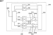
- FIG. 27 is a configuration diagram of a communication device and a high-frequency front-end circuit according to the present invention.
- FIG. 1 is a schematic plan view of an acoustic wave device according to an embodiment of the present invention.
- FIG. 2A is a circuit diagram of an acoustic wave device according to an embodiment of the present invention.
- FIG. 2B is a schematic plan view showing an electrode structure of a 1-port type acoustic wave resonator.
- the acoustic wave device 1 includes a LiNbO 3 substrate 2 as a piezoelectric substrate. A transmission filter 3 and a reception filter 4 are formed on the LiNbO 3 substrate 2.
- the elastic wave device 1 is a duplexer having a transmission filter 3 and a reception filter 4. The elastic wave device 1 uses Rayleigh waves.
- the elastic wave device 1 has an antenna terminal 5.
- a common terminal 6 is connected to the antenna terminal 5.
- a transmission filter 3 is configured between the common terminal 6 and the transmission terminal 7.
- a reception filter 4 is configured between the common terminal 6 and the reception terminal 8.
- the transmission filter 3 has a ladder type circuit configuration. Specifically, the transmission filter 3 includes series arm resonators S1 to S4 and parallel arm resonators P1 to P4.
- the series arm resonators S 1 to S 4 are connected in series between the antenna terminal 5 and the transmission terminal 7.
- the series arm resonators S1 to S4 and the parallel arm resonators P1 to P4 are indicated by a symbol in which X is surrounded by a rectangular frame.
- the parallel arm resonator P1 is connected between the connection point of the transmission terminal 7 and the series arm resonator S1 and the ground potential.
- the parallel arm resonator P2 is connected between the connection point of the series arm resonator S1 and the series arm resonator S2 and the ground potential.
- the parallel arm resonator P3 is connected between the connection point of the series arm resonator S2 and the series arm resonator S3 and the ground potential.
- the parallel arm resonator P4 is connected between the connection point of the series arm resonator S3 and the series arm resonator S4 and the ground potential.
- the series arm resonators S1 to S4 and the parallel arm resonators P1 to P4 are composed of 1-port type acoustic wave resonators.
- the 1-port type acoustic wave resonator has an electrode structure shown in FIG. Specifically, the IDT electrode 9 and the reflectors 10 and 11 disposed on both sides of the IDT electrode 9 in the elastic wave propagation direction are formed on the LiNbO 3 substrate 2. Thereby, a 1-port elastic wave resonator is configured.
- the reflectors 10 and 11 do not need to be provided.
- a 1-port type acoustic wave resonator 12 as a trap is connected to the common terminal 6.
- 3IDT type longitudinally coupled resonator type acoustic wave filter units 13 and 14 are provided between the 1-port type acoustic wave resonator 12 and the receiving terminal 8.
- the longitudinally coupled resonator type acoustic wave filter units 13 and 14 are cascade-connected to each other.
- Each of the longitudinally coupled resonator type acoustic wave filter units 13 and 14 is constituted by three IDT electrodes.
- the longitudinally coupled resonator type acoustic wave filter sections 13 and 14 may be a 5IDT type constituted by five IDT electrodes or an nIDT type constituted by n IDT electrodes. (N> 1).
- the transmission filter 3 is a ladder circuit and the reception filter 4 is a longitudinally coupled resonator type acoustic wave filter
- the transmission filter 3 may be a longitudinally coupled resonator type acoustic wave filter
- the reception filter 4 may be a ladder type circuit. Good.
- FIG. 3 is a schematic cross-sectional view showing a first elastic wave resonator constituting a series arm resonator in the elastic wave device according to the embodiment of the present invention.
- FIG. 4 is a schematic cross-sectional view showing a second elastic wave resonator constituting a parallel arm resonator in the elastic wave device according to the embodiment of the present invention.
- the first acoustic wave resonator 20 includes a LiNbO 3 substrate 2, a first IDT electrode 21, a first dielectric film 22, and a first frequency adjustment film 23.
- the first IDT electrode 21 On the main surface 2a of the LiNbO 3 substrate 2, the first IDT electrode 21 is provided.
- a first dielectric film 22 is provided so as to cover the first IDT electrode 21.
- a first frequency adjustment film 23 is provided on the first dielectric film 22.
- the second acoustic wave resonator 30 includes a LiNbO 3 substrate 2, a second IDT electrode 31, a second dielectric film 32, and a second frequency adjustment film 33.
- a second IDT electrode 31 is provided on the main surface 2 a of the LiNbO 3 substrate 2.
- a second dielectric film 32 is provided so as to cover the second IDT electrode 31.
- a second frequency adjustment film 33 is provided on the second dielectric film 32.
- the first elastic wave resonator 20 and the second elastic wave resonator 30 share the LiNbO 3 substrate 2.
- the thickness t1 of the first dielectric film 22 in the first acoustic wave resonator 20 is equal to the thickness t2 of the second dielectric film 32 in the second acoustic wave resonator 30.
- Thicker (t1> t2) the thickness t2 of the second dielectric film 32 may be larger than the thickness t1 of the first dielectric film 22. That is, the thickness t1 of the first dielectric film 22 and the thickness t2 of the second dielectric film 32 need only be different.
- the thickness t1 of the first dielectric film 22 and the thickness t2 of the second dielectric film 32 are different, the steepness can be improved in the filter characteristics, and The pass bandwidth can be expanded.
- ⁇ f difference between the resonance frequency and the antiresonance frequency of the elastic wave resonator constituting the series arm resonator.
- ⁇ f difference between the resonance frequency and the antiresonance frequency of the elastic wave resonator constituting the series arm resonator.
- ⁇ f can be reduced by increasing the thickness of the dielectric film covering the main surface of the piezoelectric substrate (LiNbO 3 substrate) and the IDT electrode, the thickness of the dielectric film on the series arm resonator is increased. .
- the bandwidth of the filter is reduced. Therefore, it is desirable to increase ⁇ f of the acoustic wave resonator constituting the parallel arm resonator. For this purpose, the thickness of the dielectric film on the parallel arm resonator is reduced.
- the steepness in the filter characteristics can be increased and the passband width can be expanded.
- the film thickness of the dielectric film covering the IDT electrode in the 1-port type acoustic wave resonator 12 in FIG. 2A is set to cover the IDT electrode in the longitudinally coupled resonator type elastic wave filter units 13 and 14. By making it thicker than the thickness of the dielectric film, it is possible to increase the steepness in the filter characteristics and to widen the passband width.
- the steepness can be enhanced in the filter characteristics, and The pass bandwidth can be expanded.
- a method for making the thickness t1 of the first dielectric film 22 different from the thickness t2 of the second dielectric film 32 on the same LiNbO 3 substrate 2 is not particularly limited. For example, the following method is used. Is mentioned.
- the first IDT electrode 21 and the second IDT electrode 31 are formed on the LiNbO 3 substrate 2. Note that when the first IDT electrode 21 and the second IDT electrode 31 are formed, the first IDT electrode 21 and the second IDT electrode 31 are simultaneously formed. Therefore, the 1st IDT electrode 21 and the 2nd IDT electrode 31 are comprised by the same electrode material and the same thickness.
- the same electrode material of the first IDT electrode 21 and the second IDT electrode 31 means that the first IDT electrode 21 and the second IDT electrode 31 are formed simultaneously. Therefore, the case where impurities are mixed in the manufacturing process is also included.
- first IDT electrode 21 and the second IDT electrode 31 means that the first IDT electrode 21 and the second IDT electrode 31 are formed simultaneously. Also included are errors in thickness that occur during the manufacturing and mounting processes.
- a dielectric film is formed so as to cover the first IDT electrode 21 and the second IDT electrode 31 on the LiNbO 3 substrate 2. Subsequently, a resist film is formed on the dielectric film of the acoustic wave resonator whose thickness is to be increased. Next, the thickness of the portion of the dielectric film where the resist film is not formed is reduced by etching the dielectric film. Finally, the resist film is removed to obtain dielectric films having different thicknesses.
- a resist film may be formed on the dielectric film of the acoustic wave resonator whose thickness is to be reduced, and a dielectric film may be further formed thereon. . Even in this case, dielectric films having different thicknesses can be obtained by removing the resist.
- all the series arm resonators S1 to S4 are constituted by the first elastic wave resonator 20. Further, all the parallel arm resonators P 1 to P 4 are constituted by the second elastic wave resonator 30.
- at least one series arm resonator among the series arm resonators S1 to S4 may be constituted by the first elastic wave resonator 20.
- at least one parallel arm resonator among the parallel arm resonators P1 to P4 may be configured by the second elastic wave resonator 30.
- At least one resonator constituting the transmission filter 3 is constituted by the first elastic wave resonator 20, and at least one resonator constituting the reception filter 4 is constituted by the second elastic wave resonator 30. It may be. In any case, the effects of the present invention can be obtained.
- the first IDT electrode 21 and the second IDT electrode 31 are composed of the same electrode material and the same thickness.
- the material of the first IDT electrode 21 and the second IDT electrode 31 is not particularly limited.
- the first IDT electrode 21 and the second IDT electrode 31 may be a single-layer metal film or a stacked metal film in which two or more kinds of metal films are stacked.
- the first IDT electrode 21 and the second IDT electrode 31 are composed of the adhesion layer 41, the main electrode 42, the adhesion layer 43, the conductive auxiliary film 44, and the adhesion layer 45 in this order from the LiNbO 3 substrate 2 side. It is the laminated metal film laminated
- the main electrode 42 is an electrode layer that occupies the largest mass among the IDT electrodes.
- adhesion layers 41, 43, 45 for example, Ti, Cr, NiCr, or the like can be used.
- the material of the main electrode 42 is not particularly limited, and a metal having a relatively high density, such as Au, Pt, Ag, Ta, W, Ni, Ru, Pd, Cr, Mo, Zn, Cu, or an alloy thereof is used. be able to.
- the material of the conductive auxiliary film 44 is not particularly limited, and for example, Al, Cu, or an alloy thereof can be used.
- adhesion layers 41, 43, and 45 and the conductive auxiliary film 44 may not be provided.
- the first dielectric film 22 and the second dielectric film 32 have a function of improving frequency temperature characteristics.
- the material of the first dielectric film 22 and the second dielectric film 32 is not particularly limited, and for example, a material mainly composed of silicon oxide or silicon oxynitride can be used.
- a main component is a component contained 50% or more.
- both the first dielectric film 22 and the second dielectric film 32 are silicon oxide films.
- the first frequency adjustment film 23 and the second frequency adjustment film 33 have a function of adjusting the frequency.
- the material of the first frequency adjustment film 23 and the second frequency adjustment film 33 is not particularly limited, and for example, silicon nitride or aluminum oxide can be used. In the present embodiment, the first frequency adjustment film 23 and the second frequency adjustment film 33 are both silicon nitride films.
- the first frequency adjustment film 23 and the second frequency adjustment film 33 may not be provided.
- the propagation direction of the elastic wave at 30 coincides. More specifically, the propagation direction of the elastic wave in the first elastic wave resonator 20 is the propagation direction A1 shown in FIG. Further, the propagation direction of the elastic wave in the second elastic wave resonator 30 is a propagation direction A2 shown in FIG. In FIG. 1, the propagation direction A1 and the propagation direction A2 coincide.
- match means that the angle formed by the propagation direction A1 and the propagation direction A2 is within a range smaller than 2 °, and the angle formed by the propagation direction A1 and the propagation direction A2 is complete. The case where it does not match is also included. However, in this embodiment, the propagation direction A1 is completely coincident with the propagation direction A2.
- the elastic wave propagation direction A 1 in the first elastic wave resonator 20 coincides with the elastic wave propagation direction A 2 in the second elastic wave resonator 30. Can be achieved.
- the Euler angles ( ⁇ , ⁇ , ⁇ ) of the LiNbO 3 substrate 2 are in the range of (0 ° ⁇ 5 °, ⁇ , 0 ° ⁇ 10 °).
- ⁇ in the Euler angles ( ⁇ , ⁇ , ⁇ ) of the LiNbO 3 substrate 2 satisfies the following formula (1) in the range of 0.055 ⁇ ⁇ T ⁇ r ⁇ 0.10 ⁇ .
- T is the thickness of the main electrode 42 in the first IDT electrode 21 and the second IDT electrode 31.
- the first IDT electrode 21 and the second IDT electrode 31 are intended to be configured with the same electrode material and the same thickness, but the components of the electrode material are partially different in the manufacturing process and the mounting process.
- the film thickness may change or the film thickness may be different. In that case, either thickness may be T, and either density may be r.
- the thickness is a thickness that is normalized by a wavelength ⁇ determined by the electrode finger pitch of the IDT electrode.
- R is a density ratio ( ⁇ / ⁇ Pt ) between the density ( ⁇ ) of the main electrode 42 and the density ( ⁇ Pt ) of Pt .
- the elastic wave device 1 since the Euler angle ⁇ of the LiNbO 3 substrate 2 is in the above range, spurious due to SH waves can be suppressed. Therefore, the elastic wave device 1 has steep filter characteristics and a wide pass band, and can suppress spurious due to SH waves while achieving downsizing.
- ⁇ at the Euler angles ( ⁇ , ⁇ , ⁇ ) of the LiNbO 3 substrate 2 is preferably in the range of ⁇ 2 ° or more and 2 ° or less.
- Euler angle ⁇ is within the above range, spurious vibrations different from those caused by SH waves can be further suppressed.
- FIG. 5 is a schematic plan view when the propagation direction of the elastic wave in the second elastic wave resonator is tilted by 1 ° with respect to the propagation direction of the elastic wave in the first elastic wave resonator.
- FIG. 6 is a schematic plan view when the propagation direction of the elastic wave in the second elastic wave resonator is inclined by 2 ° with respect to the propagation direction of the elastic wave in the first elastic wave resonator. 5 and 6, the end 2b outside the broken line in the LiNbO 3 substrate 2 is a portion where an electrode pattern cannot be formed.
- the parallel arm resonators P1 to P4 are tilted by 2 ° or more, the space for providing the resonators and the routing wirings 15 must be expanded, and it is difficult to reduce the size. Further, if the width of the routing wiring 15 is narrowed in order to secure a space, the electrical resistance of the routing wiring 15 is increased, and the characteristics of the acoustic wave device 1 may be deteriorated.
- the angle formed by the elastic wave propagation direction A1 in the first elastic wave resonator 20 and the elastic wave propagation direction A2 in the second elastic wave resonator 30 is 2. It is within the range of less than ° and it is consistent. Therefore, the acoustic wave device 1 can be reduced in size, and the characteristics are hardly deteriorated.
- the following acoustic wave resonator was designed in the structure shown in FIG.
- the adhesion layers 41, 43, and 45 are not used.
- First IDT electrode 21 Duty ratio: 0.60 Main electrode 42 ... Pt film, thickness: 0.075 ⁇ Conductive auxiliary film 44... Al film, thickness: 0.08 ⁇ First dielectric film 22: SiO 2 film, thickness: adjusted in the range of 0.2 ⁇ to 0.6 ⁇ First frequency adjustment film 23: SiN film, thickness: 0.01 ⁇ Elastic wave used... Rayleigh wave
- the Euler angle ⁇ is fixed at 30 °, the thickness of the SiO 2 film is changed within the range of 0.2 ⁇ to 0.6 ⁇ , and impedance characteristics and return loss characteristics are measured. did.
- (a) is a diagram showing impedance characteristics when the thickness of the SiO 2 film is changed for each figure, and (b) is a diagram showing its return loss characteristics. 7 to 11, the thicknesses of the SiO 2 films are 0.2 ⁇ , 0.3 ⁇ , 0.4 ⁇ , 0.5 ⁇ , and 0.6 ⁇ , respectively.
- the thickness of the SiO 2 film is fixed to 0.3 ⁇ , and the Euler angle ⁇ is changed within the range of 27.5 ° to 31.5 °, and impedance characteristics and return loss are determined. Characteristics were measured.
- FIG. 21 is a diagram illustrating the relationship between the Euler angle ⁇ and the ratio band of the SH wave.
- FIG. 21 shows the results when an acoustic wave resonator having the same design as that shown in FIGS. 12 to 20 is used.
- the ratio band of the SH wave is a value indicating the magnitude of spurious due to the SH wave. From FIG. 21, it can be seen that when the Euler angle ⁇ is 28.5 ° or more and 31.0 ° or less, the specific band of the SH wave is 0.005% or less. From this, it can be seen that if the specific band of the SH wave is 0.005% or less, the spurious due to the SH wave can be sufficiently reduced. Therefore, the Euler angle ⁇ range in which the SH wave specific band is 0.005% or less is the Euler angle ⁇ range in which the spurious due to the SH wave can be sufficiently reduced.
- an acoustic wave resonator having a different thickness of the SiO 2 film is used. Therefore, ⁇ at the Euler angle at which the SH wave specific band is 0.005% or less regardless of the thickness of the SiO 2 film. What is necessary is just to obtain
- FIG. 22 is a diagram showing the relationship between the Euler angle ⁇ and the SH wave ratio band when the thickness of the SiO 2 film is changed. Note that FIG. 22 shows the results when an elastic wave resonator having the same design as that of FIG. 21 is used except that the thickness of the SiO 2 film is changed.
- the electromechanical coupling coefficient of the SH wave varies depending on the thickness of the SiO 2 film, from FIG. 22, when the Euler angle ⁇ is 29.1 ° or more and 30.9 ° or less, regardless of the thickness of the SiO 2 film, It can be seen that the spurious due to the SH wave can be made sufficiently small.
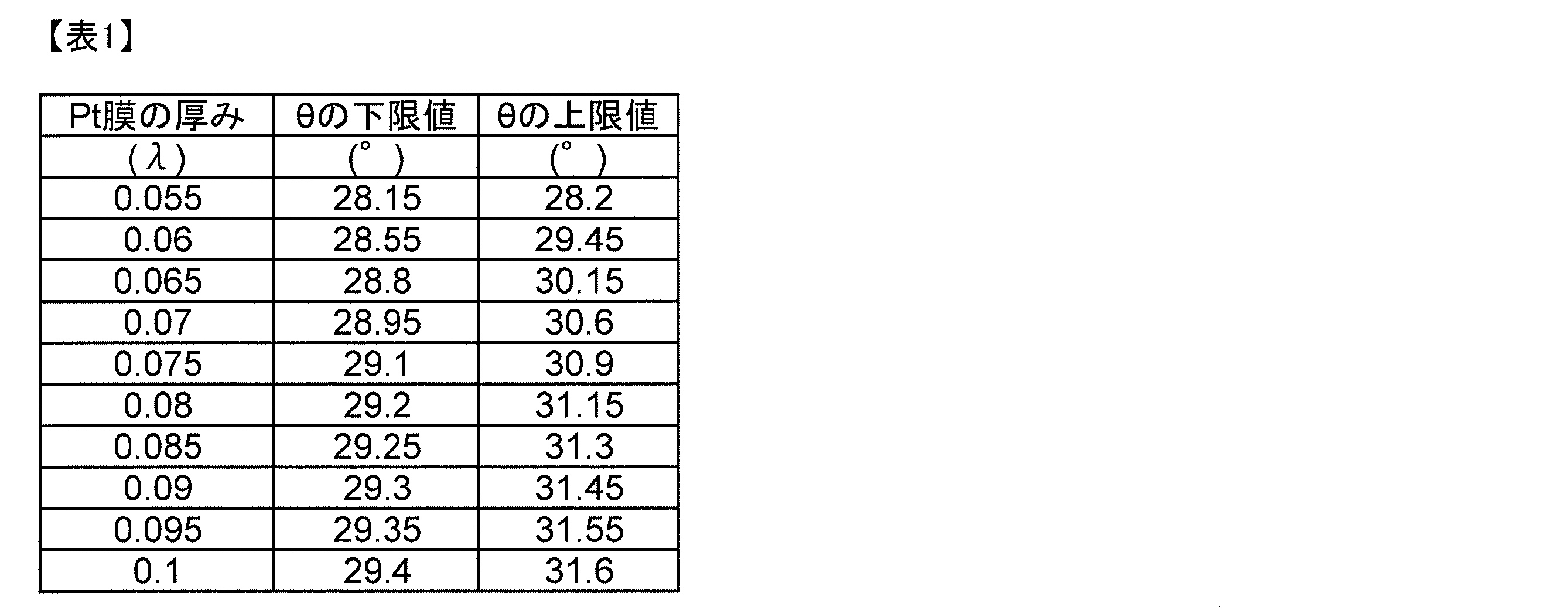
- the lower limit value and upper limit value of ⁇ in the Euler angle obtained by changing the thickness of the Pt film as the main electrode 42 are shown in Table 1 below.
- the lower limit value and the upper limit value of ⁇ in the Euler angle are values at which the SH wave specific band is 0.005% or less regardless of the thickness of the SiO 2 film.
- FIG. 23 is a diagram showing the relationship between the Euler angle ⁇ and the thickness of the Pt film.
- FIG. 23 is a plot of the lower limit value and upper limit value of ⁇ in Table 1 for the thickness of the Pt film and the Euler angle.
- a curve indicated by an arrow A in FIG. 23 is a curve obtained by plotting the lower limit value of ⁇ in the Euler angle.
- the curve indicated by the arrow A is represented by the formula: ⁇ 0.033 / (T Pt ⁇ 0.037) +29.99, where T Pt is the thickness of the Pt film.
- a curve indicated by an arrow B in FIG. 23 is a curve obtained by plotting the upper limit value of ⁇ in the Euler angle.
- the curve indicated by the arrow B is represented by the formula: ⁇ 0.050 / (T Pt ⁇ 0.043) +32.45, where T Pt is the thickness of the Pt film.
- T Pt is the thickness of the Pt film.
- a region surrounded by a curve indicated by an arrow A and a curve indicated by an arrow B is a region where spurious due to SH waves can be sufficiently suppressed.
- a region where the spurious due to the SH wave can be sufficiently suppressed is expressed by the following equation (2).
- the lower limit of the thickness of the Pt film is the intersection of the curve indicated by the arrow A and the curve indicated by the arrow B, and is 0.055 ⁇ . If the thickness of the Pt film, which is the main electrode 42, becomes too large, the aspect ratio of the IDT electrode becomes large, making it difficult to form the IDT electrode. In addition, since it may cause voids and cracks in the dielectric film on the IDT electrode, the upper limit of the thickness of the Pt film is 0.10 ⁇ .
- T ⁇ r is in the range of 0.055 ⁇ ⁇ T ⁇ r ⁇ 0.10 ⁇ .
- FIGS. 24 to 26 show the results when using an acoustic wave resonator designed as follows. In the designed acoustic wave resonator, the adhesion layers 41, 43, and 45 are not used.
- ⁇ is preferably close to 0 °.
- the elastic wave device of the above embodiment can be used as a duplexer for a high-frequency front end circuit. This example is described below.
- FIG. 27 is a configuration diagram of the communication device and the high-frequency front-end circuit.
- components connected to the high-frequency front-end circuit 230 for example, the antenna element 202 and the RF signal processing circuit (RFIC) 203 are also shown.
- the high-frequency front end circuit 230 and the RF signal processing circuit 203 constitute a communication device 240.
- the communication device 240 may include a power supply, a CPU, and a display.
- the high-frequency front-end circuit 230 includes a switch 225, duplexers 201A and 201B, filters 231, 232, low-noise amplifier circuits 214, 224, and power amplifier circuits 234a, 234b, 244a, 244b. Note that the high-frequency front-end circuit 230 and the communication device 240 in FIG. 27 are examples of the high-frequency front-end circuit and the communication device, and are not limited to this configuration.
- the duplexer 201A includes filters 211 and 212.
- the duplexer 201B includes filters 221 and 222.
- the duplexers 201 ⁇ / b> A and 201 ⁇ / b> B are connected to the antenna element 202 via the switch 225.
- the said elastic wave apparatus may be duplexers 201A and 201B, and may be filters 211, 212, 221 and 222.
- the elastic wave device is also applicable to a multiplexer having three or more filters, such as a triplexer in which the antenna terminals of three filters are shared, and a hexaplexer in which the antenna terminals of six filters are shared. Can do.
- the acoustic wave device includes an acoustic wave resonator, a filter, a duplexer, and a multiplexer including three or more filters.
- the multiplexer is not limited to the configuration including both the transmission filter and the reception filter, and may be configured to include only the transmission filter or only the reception filter.
- the switch 225 connects the antenna element 202 and a signal path corresponding to a predetermined band in accordance with a control signal from a control unit (not shown), and is configured by, for example, a SPDT (Single Pole Double Throw) type switch. .
- a SPDT Single Pole Double Throw
- the number of signal paths connected to the antenna element 202 is not limited to one and may be plural. That is, the high frequency front end circuit 230 may support carrier aggregation.
- the low noise amplifier circuit 214 is a reception amplification circuit that amplifies a high frequency signal (here, a high frequency reception signal) via the antenna element 202, the switch 225, and the duplexer 201A and outputs the amplified signal to the RF signal processing circuit 203.
- the low noise amplifier circuit 224 is a reception amplification circuit that amplifies a high-frequency signal (here, a high-frequency reception signal) that has passed through the antenna element 202, the switch 225, and the duplexer 201B, and outputs the amplified signal to the RF signal processing circuit 203.
- the power amplifier circuits 234a and 234b are transmission amplifier circuits that amplify the high frequency signal (here, the high frequency transmission signal) output from the RF signal processing circuit 203 and output the amplified signal to the antenna element 202 via the duplexer 201A and the switch 225.
- the power amplifier circuits 244a and 244b are transmission amplifier circuits that amplify the high-frequency signal (here, the high-frequency transmission signal) output from the RF signal processing circuit 203 and output the amplified signal to the antenna element 202 via the duplexer 201B and the switch 225. .
- the RF signal processing circuit 203 performs signal processing on the high-frequency reception signal input from the antenna element 202 via the reception signal path by down-conversion or the like, and outputs a reception signal generated by the signal processing.
- the RF signal processing circuit 203 performs signal processing on the input transmission signal by up-conversion or the like, and outputs a high-frequency transmission signal generated by the signal processing to the low noise amplifier circuit 224.
- the RF signal processing circuit 203 is, for example, an RFIC.
- the communication apparatus may include a BB (baseband) IC. In this case, the BBIC processes the received signal processed by the RFIC.
- the BBIC processes the transmission signal and outputs it to the RFIC.
- the reception signal processed by the BBIC and the transmission signal before the signal processing by the BBIC are, for example, an image signal or an audio signal.
- the high-frequency front end circuit 230 may include other circuit elements between the above-described components.
- the high-frequency front end circuit 230 may include a duplexer according to a modification of the duplexers 201A and 201B instead of the duplexers 201A and 201B.
- the filters 231 and 232 in the communication device 240 are connected between the RF signal processing circuit 203 and the switch 225 without passing through the low noise amplifier circuits 214 and 224 and the power amplifier circuits 234a, 234b, 244a and 244b.
- the filters 231 and 232 are also connected to the antenna element 202 via the switch 225, similarly to the duplexers 201A and 201B.
- the high-frequency front-end circuit 230 and the communication device 240 configured as described above, by including the elastic wave device of the present invention, an acoustic wave resonator, a filter, a duplexer, a multiplexer including three or more filters, and the like.
- the elastic wave device of the present invention by including the elastic wave device of the present invention, an acoustic wave resonator, a filter, a duplexer, a multiplexer including three or more filters, and the like.
- the elastic wave device, the high-frequency front end circuit, and the communication device according to the embodiment of the present invention have been described with reference to the embodiment.
- the present invention can be realized by combining arbitrary components in the above embodiment. And various modifications incorporating various modifications conceivable by those skilled in the art within the scope of the present invention without departing from the gist of the present invention, and various high frequency front end circuits and communication devices according to the present invention. Equipment is also included in the present invention.
- the present invention can be widely used in communication devices such as mobile phones as an elastic wave resonator, a filter, a duplexer, a multiplexer, a front end circuit, and a communication device that can be applied to a multiband system.
- acoustic wave device 2 ... LiNbO 3 substrate 2a ... main surface 2b ... end 3 ... transmission filter 4 ... reception filter 5 ... antenna terminal 6 ... common terminal 7 ... transmission terminal 8 ... receiving terminal 9 ...
- IDT electrodes 10 and 11 ... Reflector 12 ... 1-port type acoustic wave resonators 13 and 14... Longitudinally coupled resonator type acoustic wave filter unit 15... Routing wires 20 and 30... First and second acoustic wave resonators 21 and 31. 2 IDT electrodes 22, 32... 1, 2nd dielectric film 23, 33... 1, 2nd frequency adjustment film 41, 43, 45 ... adhesion layer 42 ... main electrode 44 ...
Landscapes
- Physics & Mathematics (AREA)
- Acoustics & Sound (AREA)
- Engineering & Computer Science (AREA)
- Computer Networks & Wireless Communication (AREA)
- Signal Processing (AREA)
- Chemical & Material Sciences (AREA)
- Materials Engineering (AREA)
- Surface Acoustic Wave Elements And Circuit Networks Thereof (AREA)
Abstract
Description
図1は、本発明の一実施形態に係る弾性波装置の模式的平面図である。図2(a)は、本発明の一実施形態に係る弾性波装置の回路図である。図2(b)は、1ポート型の弾性波共振子の電極構造を示す模式的平面図である。
第1のIDT電極21…デューティ比:0.60
主電極42…Pt膜、厚み:0.075λ
導電補助膜44…Al膜、厚み:0.08λ
第1の誘電体膜22…SiO2膜、厚み:0.2λ~0.6λの範囲で調整
第1の周波数調整膜23…SiN膜、厚み:0.01λ
利用する弾性波…レイリー波
第1のIDT電極21…デューティ比:0.60
主電極42…Pt膜、厚み:0.075λ
導電補助膜44…Al膜、厚み:0.08λ
第1の誘電体膜22…SiO2膜、厚み:0.3λ
第1の周波数調整膜23…SiN膜、厚み:0.01λ
上記実施形態の弾性波装置は、高周波フロントエンド回路のデュプレクサなどとして用いることができる。この例を下記において説明する。
2…LiNbO3基板
2a…主面
2b…端部
3…送信フィルタ
4…受信フィルタ
5…アンテナ端子
6…共通端子
7…送信端子
8…受信端子
9…IDT電極
10,11…反射器
12…1ポート型弾性波共振子
13,14…縦結合共振子型弾性波フィルタ部
15…引き回し配線
20,30…第1,第2の弾性波共振子
21,31…第1,第2のIDT電極
22,32…第1,第2の誘電体膜
23,33…第1,第2の周波数調整膜
41,43,45…密着層
42…主電極
44…導電補助膜
201A,201B…デュプレクサ
202…アンテナ素子
203…RF信号処理回路
211,212…フィルタ
214…ローノイズアンプ回路
221,222…フィルタ
224…ローノイズアンプ回路
225…スイッチ
230…高周波フロントエンド回路
231,232…フィルタ
234a,234b…パワーアンプ回路
240…通信装置
244a,244b…パワーアンプ回路
A1,A2…伝搬方向
P1~P4…並列腕共振子
S1~S4…直列腕共振子
Claims (8)
- LiNbO3基板と、
前記LiNbO3基板上に設けられた第1のIDT電極と、前記第1のIDT電極を覆うように設けられた第1の誘電体膜とを有する、第1の弾性波共振子と、
前記LiNbO3基板上に設けられた第2のIDT電極と、前記第2のIDT電極を覆うように設けられた第2の誘電体膜とを有する、第2の弾性波共振子と、
を備え、
レイリー波を利用しており、
前記第1の誘電体膜の厚みが、前記第2の誘電体膜の厚みと異なっており、
前記第1の弾性波共振子における弾性波の伝搬方向が、前記第2の弾性波共振子における弾性波の伝搬方向と一致しており、
前記LiNbO3基板のオイラー角(φ,θ,ψ)が、(0°±5°,θ,0°±10°)の範囲内であり、
前記第1のIDT電極及び前記第2のIDT電極は、主電極を有し、
前記第1のIDT電極及び前記第2のIDT電極のうち少なくとも一方の電極指ピッチで定まる波長λにより規格化してなる前記主電極の厚みをTとし、前記主電極の密度(ρ)とPtの密度(ρPt)との密度比(ρ/ρPt)をrとしたときに、
前記LiNbO3基板のオイラー角(φ,θ,ψ)におけるθが、0.055λ≦T×r≦0.10λの範囲において、下記式(1)を満たしている、弾性波装置。
-0.033/(T×r-0.037)+29.99≦θ≦-0.050/(T×r-0.043)+32.45 …(1) - 前記第1のIDT電極及び前記第2のIDT電極が、同じ電極材料、かつ同じ厚みで構成されている、請求項1に記載の弾性波装置。
- 前記LiNbO3基板のオイラー角(φ,θ,ψ)におけるψが、-2°以上、2°以下の範囲内にある、請求項1又は2に記載の弾性波装置。
- 前記第1の誘電体膜及び前記第2の誘電体膜は、それぞれ酸化ケイ素を主成分とする、請求項1~3のいずれか1項に記載の弾性波装置。
- 前記第1の弾性波共振子は、直列腕共振子であり、
前記第2の弾性波共振子は、並列腕共振子であり、
少なくとも前記第1の弾性波共振子と前記第2の弾性波共振子とにより、ラダー型フィルタを形成する、請求項1~4のいずれか1項に記載の弾性波装置。 - 前記弾性波装置は、
前記第1の弾性波共振子を有する送信フィルタと、
前記第2の弾性波共振子を有する受信フィルタと、
を備える、デュプレクサである、請求項1~4のいずれか1項に記載の弾性波装置。 - 請求項1~6のいずれか1項に記載の弾性波装置と、
パワーアンプと、
を備える、高周波フロントエンド回路。 - 請求項7に記載の高周波フロントエンド回路と、
RF信号処理回路と、
を備える、通信装置。
Priority Applications (6)
| Application Number | Priority Date | Filing Date | Title |
|---|---|---|---|
| CN201780078435.XA CN110089030B (zh) | 2016-12-20 | 2017-10-17 | 弹性波装置、高频前端电路以及通信装置 |
| JP2018557570A JP6791266B2 (ja) | 2016-12-20 | 2017-10-17 | 弾性表面波装置、高周波フロントエンド回路及び通信装置 |
| KR1020197016513A KR102280381B1 (ko) | 2016-12-20 | 2017-10-17 | 탄성파 장치, 고주파 프론트 엔드 회로 및 통신 장치 |
| US16/443,919 US10840880B2 (en) | 2016-12-20 | 2019-06-18 | Elastic wave device, high frequency front-end circuit, and communication apparatus |
| US17/065,572 US11482984B2 (en) | 2016-12-20 | 2020-10-08 | Elastic wave device, high frequency front-end circuit, and communication apparatus |
| US17/942,212 US11855606B2 (en) | 2016-12-20 | 2022-09-12 | Elastic wave device, high frequency front-end circuit, and communication apparatus |
Applications Claiming Priority (2)
| Application Number | Priority Date | Filing Date | Title |
|---|---|---|---|
| JP2016246267 | 2016-12-20 | ||
| JP2016-246267 | 2016-12-20 |
Related Child Applications (1)
| Application Number | Title | Priority Date | Filing Date |
|---|---|---|---|
| US16/443,919 Continuation US10840880B2 (en) | 2016-12-20 | 2019-06-18 | Elastic wave device, high frequency front-end circuit, and communication apparatus |
Publications (1)
| Publication Number | Publication Date |
|---|---|
| WO2018116602A1 true WO2018116602A1 (ja) | 2018-06-28 |
Family
ID=62626136
Family Applications (1)
| Application Number | Title | Priority Date | Filing Date |
|---|---|---|---|
| PCT/JP2017/037558 Ceased WO2018116602A1 (ja) | 2016-12-20 | 2017-10-17 | 弾性波装置、高周波フロントエンド回路及び通信装置 |
Country Status (5)
| Country | Link |
|---|---|
| US (3) | US10840880B2 (ja) |
| JP (1) | JP6791266B2 (ja) |
| KR (1) | KR102280381B1 (ja) |
| CN (1) | CN110089030B (ja) |
| WO (1) | WO2018116602A1 (ja) |
Cited By (7)
| Publication number | Priority date | Publication date | Assignee | Title |
|---|---|---|---|---|
| WO2020261978A1 (ja) * | 2019-06-24 | 2020-12-30 | 株式会社村田製作所 | 弾性表面波装置及びフィルタ装置 |
| US20210399714A1 (en) * | 2020-06-17 | 2021-12-23 | Resonant Inc. | Transversely-excited film bulk acoustic resonators with three-layer electrodes |
| JP2022506474A (ja) * | 2018-10-31 | 2022-01-17 | レゾナント インコーポレイテッド | 音響反射型の横方向に励振される薄膜バルク弾性波共振子 |
| WO2022075415A1 (ja) * | 2020-10-08 | 2022-04-14 | 株式会社村田製作所 | 弾性波装置 |
| WO2023002909A1 (ja) * | 2021-07-19 | 2023-01-26 | 株式会社村田製作所 | 複合フィルタ装置 |
| US11870424B2 (en) | 2018-06-15 | 2024-01-09 | Murata Manufacturing Co., Ltd. | Filters using transversly-excited film bulk acoustic resonators with frequency-setting dielectric layers |
| US12074584B2 (en) | 2020-05-28 | 2024-08-27 | Murata Manufacturing Co., Ltd. | Transversely-excited film bulk acoustic resonators with two-layer electrodes |
Families Citing this family (2)
| Publication number | Priority date | Publication date | Assignee | Title |
|---|---|---|---|---|
| KR102280381B1 (ko) * | 2016-12-20 | 2021-07-22 | 가부시키가이샤 무라타 세이사쿠쇼 | 탄성파 장치, 고주파 프론트 엔드 회로 및 통신 장치 |
| CN118826685B (zh) * | 2024-09-19 | 2024-12-17 | 天通瑞宏科技有限公司 | 一种弹性波谐振器、滤波器、多工器及射频前端电路 |
Citations (2)
| Publication number | Priority date | Publication date | Assignee | Title |
|---|---|---|---|---|
| JP2008079227A (ja) * | 2006-09-25 | 2008-04-03 | Fujitsu Media Device Kk | フィルタおよび分波器 |
| JP2015012324A (ja) * | 2013-06-26 | 2015-01-19 | 株式会社村田製作所 | 弾性境界波装置 |
Family Cites Families (22)
| Publication number | Priority date | Publication date | Assignee | Title |
|---|---|---|---|---|
| US5654680A (en) * | 1996-01-30 | 1997-08-05 | Motorola, Inc. | Saw-based ladder filter including multiple coUpling coefficients (K2), Method therefor and radio incorporating same |
| WO2007125734A1 (ja) | 2006-04-24 | 2007-11-08 | Murata Manufacturing Co., Ltd. | 弾性表面波装置 |
| JP2010187373A (ja) * | 2009-01-19 | 2010-08-26 | Ngk Insulators Ltd | 複合基板及びそれを用いた弾性波デバイス |
| CN104734662B (zh) * | 2009-04-22 | 2017-09-22 | 天工滤波方案日本有限公司 | 弹性波元件和使用它的电子设备 |
| JP2010278830A (ja) * | 2009-05-29 | 2010-12-09 | Murata Mfg Co Ltd | ラダー型フィルタ及びその製造方法並びにデュプレクサ |
| JP5799952B2 (ja) * | 2010-05-20 | 2015-10-28 | 日立化成株式会社 | 感光性樹脂組成物、感光性フィルム、リブパターンの形成方法、中空構造とその形成方法及び電子部品 |
| CN103329437B (zh) * | 2011-01-18 | 2016-03-16 | 株式会社村田制作所 | 弹性表面波滤波器装置 |
| JP5856408B2 (ja) * | 2011-08-22 | 2016-02-09 | 太陽誘電株式会社 | 弾性波デバイスおよびモジュール |
| WO2013061694A1 (ja) * | 2011-10-24 | 2013-05-02 | 株式会社村田製作所 | 弾性波分波器 |
| JP5690711B2 (ja) * | 2011-12-28 | 2015-03-25 | スカイワークス・パナソニック フィルターソリューションズ ジャパン株式会社 | 弾性波素子 |
| JP5784217B2 (ja) * | 2012-03-14 | 2015-09-24 | スカイワークス・パナソニック フィルターソリューションズ ジャパン株式会社 | 弾性波装置 |
| WO2013141168A1 (ja) * | 2012-03-23 | 2013-09-26 | 株式会社村田製作所 | 弾性波装置及びその製造方法 |
| KR101924025B1 (ko) * | 2014-02-04 | 2018-11-30 | 가부시키가이샤 무라타 세이사쿠쇼 | 탄성파 장치 |
| WO2016060072A1 (ja) * | 2014-10-17 | 2016-04-21 | 株式会社村田製作所 | 圧電デバイス、圧電デバイスの製造方法 |
| JP5883110B2 (ja) * | 2014-11-26 | 2016-03-09 | スカイワークス・パナソニック フィルターソリューションズ ジャパン株式会社 | 弾性波デバイスとデュプレクサ |
| CN107210732B (zh) * | 2015-01-07 | 2020-09-11 | 株式会社村田制作所 | 复合滤波器装置 |
| JP2016138761A (ja) * | 2015-01-26 | 2016-08-04 | マミヤ・オーピー・ネクオス株式会社 | 光切断法による三次元測定方法および三次元測定器 |
| FR3033462B1 (fr) * | 2015-03-04 | 2018-03-30 | Commissariat A L'energie Atomique Et Aux Energies Alternatives | Dispositif a ondes elastiques de surface comprenant un film piezoelectrique monocristallin et un substrat cristallin, a faibles coefficients viscoelastiques |
| JP2018056630A (ja) * | 2016-09-26 | 2018-04-05 | 株式会社村田製作所 | 弾性波装置、高周波フロントエンド回路及び通信装置 |
| SG11201903365SA (en) * | 2016-10-20 | 2019-05-30 | Skyworks Solutions Inc | Elastic wave device with sub-wavelength thick piezoelectric layer |
| KR102280381B1 (ko) * | 2016-12-20 | 2021-07-22 | 가부시키가이샤 무라타 세이사쿠쇼 | 탄성파 장치, 고주파 프론트 엔드 회로 및 통신 장치 |
| WO2021002157A1 (ja) * | 2019-07-03 | 2021-01-07 | 株式会社村田製作所 | 高周波モジュール及び通信装置 |
-
2017
- 2017-10-17 KR KR1020197016513A patent/KR102280381B1/ko active Active
- 2017-10-17 CN CN201780078435.XA patent/CN110089030B/zh active Active
- 2017-10-17 JP JP2018557570A patent/JP6791266B2/ja active Active
- 2017-10-17 WO PCT/JP2017/037558 patent/WO2018116602A1/ja not_active Ceased
-
2019
- 2019-06-18 US US16/443,919 patent/US10840880B2/en active Active
-
2020
- 2020-10-08 US US17/065,572 patent/US11482984B2/en active Active
-
2022
- 2022-09-12 US US17/942,212 patent/US11855606B2/en active Active
Patent Citations (2)
| Publication number | Priority date | Publication date | Assignee | Title |
|---|---|---|---|---|
| JP2008079227A (ja) * | 2006-09-25 | 2008-04-03 | Fujitsu Media Device Kk | フィルタおよび分波器 |
| JP2015012324A (ja) * | 2013-06-26 | 2015-01-19 | 株式会社村田製作所 | 弾性境界波装置 |
Cited By (11)
| Publication number | Priority date | Publication date | Assignee | Title |
|---|---|---|---|---|
| US11870424B2 (en) | 2018-06-15 | 2024-01-09 | Murata Manufacturing Co., Ltd. | Filters using transversly-excited film bulk acoustic resonators with frequency-setting dielectric layers |
| JP2022506474A (ja) * | 2018-10-31 | 2022-01-17 | レゾナント インコーポレイテッド | 音響反射型の横方向に励振される薄膜バルク弾性波共振子 |
| JP7501529B2 (ja) | 2018-10-31 | 2024-06-18 | 株式会社村田製作所 | フィルタデバイス及びフィルタデバイスを製造する方法 |
| WO2020261978A1 (ja) * | 2019-06-24 | 2020-12-30 | 株式会社村田製作所 | 弾性表面波装置及びフィルタ装置 |
| US12289093B2 (en) | 2019-06-24 | 2025-04-29 | Murata Manufacturing Co., Ltd. | Surface acoustic wave device and filter device |
| US12074584B2 (en) | 2020-05-28 | 2024-08-27 | Murata Manufacturing Co., Ltd. | Transversely-excited film bulk acoustic resonators with two-layer electrodes |
| US20210399714A1 (en) * | 2020-06-17 | 2021-12-23 | Resonant Inc. | Transversely-excited film bulk acoustic resonators with three-layer electrodes |
| US12267062B2 (en) * | 2020-06-17 | 2025-04-01 | Murata Manufacturing Co., Ltd. | Transversely-excited film bulk acoustic resonators with three-layer electrodes |
| WO2022075415A1 (ja) * | 2020-10-08 | 2022-04-14 | 株式会社村田製作所 | 弾性波装置 |
| US12537499B2 (en) | 2020-10-08 | 2026-01-27 | Murata Manufacturing Co., Ltd. | Acoustic wave device |
| WO2023002909A1 (ja) * | 2021-07-19 | 2023-01-26 | 株式会社村田製作所 | 複合フィルタ装置 |
Also Published As
| Publication number | Publication date |
|---|---|
| US11482984B2 (en) | 2022-10-25 |
| CN110089030A (zh) | 2019-08-02 |
| JPWO2018116602A1 (ja) | 2019-10-24 |
| US20230006641A1 (en) | 2023-01-05 |
| JP6791266B2 (ja) | 2020-11-25 |
| US11855606B2 (en) | 2023-12-26 |
| KR102280381B1 (ko) | 2021-07-22 |
| US20210028761A1 (en) | 2021-01-28 |
| US10840880B2 (en) | 2020-11-17 |
| CN110089030B (zh) | 2023-01-06 |
| US20190305751A1 (en) | 2019-10-03 |
| KR20190076048A (ko) | 2019-07-01 |
Similar Documents
| Publication | Publication Date | Title |
|---|---|---|
| JP6791266B2 (ja) | 弾性表面波装置、高周波フロントエンド回路及び通信装置 | |
| JP6915466B2 (ja) | 弾性波装置、高周波フロントエンド回路及び通信装置 | |
| JP6964603B2 (ja) | マルチプレクサ、高周波フロントエンド回路及び通信装置 | |
| US12273094B2 (en) | Acoustic wave device, high frequency front end circuit, and communication apparatus | |
| KR102311837B1 (ko) | 탄성파 장치, 고주파 프론트 엔드 회로 및 통신 장치 | |
| US20180091118A1 (en) | Elastic wave device, high-frequency front end circuit, and communication apparatus | |
| KR102186692B1 (ko) | 탄성파 장치, 고주파 프론트 엔드 회로 및 통신 장치 | |
| JP6601503B2 (ja) | 弾性波装置、高周波フロントエンド回路及び通信装置 | |
| WO2018123545A1 (ja) | マルチプレクサ | |
| US10680578B2 (en) | Elastic wave device, filter, multiplexer, radio-frequency front-end circuit, and communication device | |
| JP2018101849A (ja) | 弾性波装置、高周波フロントエンド回路及び通信装置 |
Legal Events
| Date | Code | Title | Description |
|---|---|---|---|
| 121 | Ep: the epo has been informed by wipo that ep was designated in this application |
Ref document number: 17883074 Country of ref document: EP Kind code of ref document: A1 |
|
| ENP | Entry into the national phase |
Ref document number: 2018557570 Country of ref document: JP Kind code of ref document: A |
|
| ENP | Entry into the national phase |
Ref document number: 20197016513 Country of ref document: KR Kind code of ref document: A |
|
| NENP | Non-entry into the national phase |
Ref country code: DE |
|
| 122 | Ep: pct application non-entry in european phase |
Ref document number: 17883074 Country of ref document: EP Kind code of ref document: A1 |