WO2018100852A1 - Condensateur - Google Patents
Condensateur Download PDFInfo
- Publication number
- WO2018100852A1 WO2018100852A1 PCT/JP2017/034232 JP2017034232W WO2018100852A1 WO 2018100852 A1 WO2018100852 A1 WO 2018100852A1 JP 2017034232 W JP2017034232 W JP 2017034232W WO 2018100852 A1 WO2018100852 A1 WO 2018100852A1
- Authority
- WO
- WIPO (PCT)
- Prior art keywords
- wall portion
- case
- capacitor
- wall
- bottom wall
- Prior art date
Links
- 239000003990 capacitor Substances 0.000 title claims abstract description 114
- 229920005989 resin Polymers 0.000 claims abstract description 30
- 239000011347 resin Substances 0.000 claims abstract description 30
- 230000002093 peripheral effect Effects 0.000 claims abstract description 8
- 239000011358 absorbing material Substances 0.000 claims description 8
- 230000000630 rising effect Effects 0.000 claims description 2
- 239000010408 film Substances 0.000 description 41
- 239000011104 metalized film Substances 0.000 description 15
- 229910052751 metal Inorganic materials 0.000 description 14
- 239000002184 metal Substances 0.000 description 14
- 230000008878 coupling Effects 0.000 description 9
- 238000010168 coupling process Methods 0.000 description 9
- 238000005859 coupling reaction Methods 0.000 description 9
- 238000000034 method Methods 0.000 description 8
- WABPQHHGFIMREM-UHFFFAOYSA-N lead(0) Chemical compound [Pb] WABPQHHGFIMREM-UHFFFAOYSA-N 0.000 description 7
- HCHKCACWOHOZIP-UHFFFAOYSA-N Zinc Chemical compound [Zn] HCHKCACWOHOZIP-UHFFFAOYSA-N 0.000 description 6
- 229910052782 aluminium Inorganic materials 0.000 description 6
- XAGFODPZIPBFFR-UHFFFAOYSA-N aluminium Chemical compound [Al] XAGFODPZIPBFFR-UHFFFAOYSA-N 0.000 description 6
- 150000002739 metals Chemical class 0.000 description 6
- 230000001629 suppression Effects 0.000 description 6
- 229910052725 zinc Inorganic materials 0.000 description 6
- 239000011701 zinc Substances 0.000 description 6
- 230000000694 effects Effects 0.000 description 5
- 210000000078 claw Anatomy 0.000 description 4
- 238000010586 diagram Methods 0.000 description 4
- 238000005476 soldering Methods 0.000 description 4
- 238000005507 spraying Methods 0.000 description 4
- 238000004804 winding Methods 0.000 description 4
- 239000004734 Polyphenylene sulfide Substances 0.000 description 3
- 239000003822 epoxy resin Substances 0.000 description 3
- 238000003780 insertion Methods 0.000 description 3
- 230000037431 insertion Effects 0.000 description 3
- 239000000463 material Substances 0.000 description 3
- 229920000647 polyepoxide Polymers 0.000 description 3
- 229920000069 polyphenylene sulfide Polymers 0.000 description 3
- 238000003466 welding Methods 0.000 description 3
- RYGMFSIKBFXOCR-UHFFFAOYSA-N Copper Chemical compound [Cu] RYGMFSIKBFXOCR-UHFFFAOYSA-N 0.000 description 2
- FYYHWMGAXLPEAU-UHFFFAOYSA-N Magnesium Chemical compound [Mg] FYYHWMGAXLPEAU-UHFFFAOYSA-N 0.000 description 2
- 239000000956 alloy Substances 0.000 description 2
- 229910045601 alloy Inorganic materials 0.000 description 2
- 229910052802 copper Inorganic materials 0.000 description 2
- 239000010949 copper Substances 0.000 description 2
- 229910052749 magnesium Inorganic materials 0.000 description 2
- 239000011777 magnesium Substances 0.000 description 2
- 238000004519 manufacturing process Methods 0.000 description 2
- 229920001187 thermosetting polymer Polymers 0.000 description 2
- 239000000853 adhesive Substances 0.000 description 1
- 230000001070 adhesive effect Effects 0.000 description 1
- 238000005452 bending Methods 0.000 description 1
- 239000000470 constituent Substances 0.000 description 1
- 238000000151 deposition Methods 0.000 description 1
- 238000007667 floating Methods 0.000 description 1
- 239000011491 glass wool Substances 0.000 description 1
- 238000005304 joining Methods 0.000 description 1
- 239000007769 metal material Substances 0.000 description 1
- 239000011490 mineral wool Substances 0.000 description 1
- 230000004048 modification Effects 0.000 description 1
- 238000012986 modification Methods 0.000 description 1
- 230000000149 penetrating effect Effects 0.000 description 1
- 238000003825 pressing Methods 0.000 description 1
Images


Classifications
-
- H—ELECTRICITY
- H01—ELECTRIC ELEMENTS
- H01G—CAPACITORS; CAPACITORS, RECTIFIERS, DETECTORS, SWITCHING DEVICES, LIGHT-SENSITIVE OR TEMPERATURE-SENSITIVE DEVICES OF THE ELECTROLYTIC TYPE
- H01G2/00—Details of capacitors not covered by a single one of groups H01G4/00-H01G11/00
- H01G2/10—Housing; Encapsulation
-
- H—ELECTRICITY
- H01—ELECTRIC ELEMENTS
- H01G—CAPACITORS; CAPACITORS, RECTIFIERS, DETECTORS, SWITCHING DEVICES, LIGHT-SENSITIVE OR TEMPERATURE-SENSITIVE DEVICES OF THE ELECTROLYTIC TYPE
- H01G4/00—Fixed capacitors; Processes of their manufacture
- H01G4/002—Details
- H01G4/224—Housing; Encapsulation
-
- H—ELECTRICITY
- H01—ELECTRIC ELEMENTS
- H01G—CAPACITORS; CAPACITORS, RECTIFIERS, DETECTORS, SWITCHING DEVICES, LIGHT-SENSITIVE OR TEMPERATURE-SENSITIVE DEVICES OF THE ELECTROLYTIC TYPE
- H01G4/00—Fixed capacitors; Processes of their manufacture
- H01G4/33—Thin- or thick-film capacitors
Definitions
- the present invention relates to a capacitor.
- a case mold type capacitor in which a capacitor element to which a bus bar is connected is housed in a case having an upper surface opened, and a filling resin such as an epoxy resin is filled in the case.
- the side surface (circumferential surface) and the bottom surface of the case can be configured by two wall portions having a gap between each other.
- a case can usually be created by joining two members.
- Patent Document 1 describes a case mold type capacitor in which a case is constituted by a resin interior case and a metal exterior case that accommodates the interior case. A coupling portion is provided on the upper side of the inner case so as to protrude outward. On the other hand, a coupling portion having a concave shape is provided on the upper side surface of the exterior case, and the coupling portion of the interior case is fitted into the coupling portion from above.
- the inner case and the outer case are combined and integrated by fastening both connecting portions with bolts or the like.
- the inner case when creating the case, the inner case is likely to be displaced from the intended position in the front-rear and left-right directions with respect to the outer case, and the gap is small at the portion where the side surface of the inner case is close to the side surface of the outer case. Prone. Thereby, there is a concern that a variation in the gap in the side surface direction (circumferential surface direction) of the case makes it difficult to obtain a stable noise suppression effect.
- an object of the present invention is to provide a capacitor that can be expected to obtain a satisfactory noise suppression effect by a case of a double wall structure.
- a capacitor according to a main aspect of the present invention includes a capacitor element, a case in which the capacitor element is accommodated, and a filling resin filled in the case.
- the case includes a bottom wall portion, a cylindrical inner wall portion that rises from the periphery of the bottom wall portion, and a cylindrical shape that surrounds the inner wall portion and extends in a direction orthogonal to the bottom wall portion.
- a case main body formed integrally with the outer wall portion, and a connecting portion that connects the inner wall portion and the outer wall portion so as to create a gap between the two wall portions, and the bottom wall of the outer wall portion
- a lid portion that closes an opening surface facing the portion so as to form a gap with the bottom wall portion.
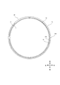
- FIG. 1A is a plan view of the film capacitor according to the first embodiment
- FIG. 1B is a cross-sectional view taken along line AA ′ of FIG.
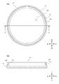
- FIG. 2A is a plan view of the case main body according to the first embodiment
- FIG. 2B is a cross-sectional view taken along the line BB ′ of FIG.
- FIG. 3 is a bottom view of the case main body according to the first embodiment.
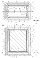
- FIG. 4A is a plan view of the lid according to the first embodiment
- FIG. 4B is a cross-sectional view taken along the line CC ′ of FIG. 4A.
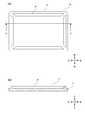
- FIG. 5 is a diagram illustrating a state in which the film capacitor is mounted on the printed board according to the first embodiment.
- FIG. 6A is a plan view of a film capacitor according to the second embodiment, and FIG. 6B is a cross-sectional view taken along the line DD ′ of FIG.
- FIG. 7A is a plan view of a case body according to the second embodiment, and FIG. 7B is a bottom view of the case body according to the second embodiment.
- FIG. 8A is a plan view of the lid according to the second embodiment, and FIG. 8B is a cross-sectional view taken along the line EE ′ of FIG. 8A.
- FIG. 9 is a diagram for explaining a film capacitor according to a modified example.
- 10A and 10B are diagrams for explaining a film capacitor according to a modification.
- the female screw portion 37 corresponds to the “first screw portion” recited in the claims.
- the male screw portion 43 corresponds to a “second screw portion” recited in the claims.
- FIG. 1 (a) is a plan view of a film capacitor 1A according to the first embodiment
- FIG. 1 (b) is a cross-sectional view taken along line AA ′ of FIG. 1 (a).
- 2A is a plan view of the case main body 30 according to the first embodiment
- FIG. 2B is a cross-sectional view taken along the line BB ′ of FIG. 2A.
- FIG. 3 is a bottom view of the case main body 30 according to the first embodiment.
- 4A is a plan view of the lid 40 according to the first embodiment
- FIG. 4B is a cross-sectional view taken along the line CC ′ of FIG. 4A.
- illustration of the filling resin 4 is omitted for the sake of convenience
- FIG. 1B the filling resin 4 is in a transparent state for convenience, and only the upper surface is drawn with diagonal lines. Yes.
- the film capacitor 1 ⁇ / b> A includes a capacitor element unit 2, a case 3, and a filling resin 4.
- the capacitor element unit 2 is accommodated in the case 3 and filled with the filling resin 4.
- the filling resin 4 is made of, for example, a thermosetting resin such as an epoxy resin, is injected into the case 3 in a molten state, and is cured when the case 3 is heated.
- the filling resin 4 covers most of the capacitor element unit 2 and protects these parts from moisture and impact.
- the capacitor element unit 2 includes a capacitor element 10 and a lead terminal portion 20 attached to the capacitor element 10.
- the capacitor element 10 is formed by stacking two metallized films on which aluminum is vapor-deposited on a dielectric film and winding the stacked metallized films, and has a substantially cylindrical shape.
- the capacitor element 10 is formed with a circular through hole 11 penetrating in the vertical direction at the center.
- the capacitor element 10 has a first electrode 12 formed on the upper end surface by spraying a metal such as zinc, and a second electrode 13 formed on the lower end surface by spraying a metal such as zinc. Is done.
- the capacitor element 10 may be formed of a metallized film in which other metal such as zinc or magnesium is vapor-deposited in addition to the metallized film in which aluminum is vapor-deposited on the dielectric film.
- condenser element 10 may be formed with the metallized film which vapor-deposited several metals among these metals, and may be formed with the metallized film vapor-deposited the alloy of these metals. .
- the lead terminal portion 20 includes a terminal mounting plate 21, a first terminal 22, a second terminal 23, a first lead wire 24, and a second lead wire 25.
- the terminal mounting plate 21 is made of a resin material and has a long plate shape in the left-right direction.
- the terminal mounting plate 21 is formed with a protruding portion 26 that protrudes downward, and the tip of the protruding portion 26 is fitted into the through hole 11 of the capacitor element 10.
- An insertion hole 27 that is connected to the through hole 11 is formed in the protrusion 26.
- the first terminal 22 and the second terminal 23 are made of a metal material having excellent conductivity, such as copper, and have a substantially L-shape.
- the first terminal 22 and the second terminal 23 are attached to both sides of the protrusion 26 on the terminal attachment plate 21.
- the first terminal 22 and the second terminal 23 protrude upward from the upper surface of the terminal mounting plate 21, and their base ends face the lower surface side of the terminal mounting plate 21.
- the first lead wire 24 electrically connects the first terminal 22 and the first electrode 12 of the capacitor element 10.
- the second lead wire 25 electrically connects the second terminal 23 and the second electrode 13 of the capacitor element 10.
- the second lead wire 25 is passed through the insertion hole 27 of the terminal mounting plate 21 and the through hole 11 of the capacitor element 10.
- Case 3 is a double-walled container having a bottomed cylindrical shape, and includes a case body 30 and a lid 40.
- the case body 30 and the lid portion 40 are formed of the same resin material having excellent moisture resistance and heat resistance, such as polyphenylene sulfide resin (PPS).
- PPS polyphenylene sulfide resin
- the case body 30 includes a circular bottom wall portion 31, a cylindrical inner wall portion 32 that rises from the peripheral edge of the bottom wall portion 31, a cylindrical outer wall portion 33 that surrounds the inner wall portion 32, an inner wall portion 32, and an outer wall portion 33. And a connecting portion 34 for connecting the two.
- the bottom wall portion 31 is formed with a recessed portion 31a that is slightly recessed on the lower surface thereof.
- a first receiving portion 35 and a second receiving portion 36 are formed on the left and right sides of the upper end portion 32a of the inner wall portion 32, respectively.
- the first receiving portion 35 and the second receiving portion 36 are each formed with three first claw portions 35a and second claw portions 36a.
- the outer wall portion 33 extends from the bottom wall portion 31 in a downward direction, that is, in a direction orthogonal to the bottom wall portion 31.
- the opening end portion 33 b of the outer wall portion 33 is located below the bottom wall portion 31.
- a female screw portion 37 is formed inside the open end portion 33b by a rib 37a that runs spirally.
- the connecting portion 34 is continuous over the entire circumference between the upper end portion 32a of the inner wall portion 32 (the end portion opposite to the bottom wall portion 31) and the upper end portion 33a of the outer wall portion 33 that faces the upper end portion 32a. They are connected to each other so that a gap S1 is formed between them.
- the lid portion 40 closes the opening surface 33 c of the outer wall portion 33 that faces the bottom wall portion 31 such that a gap S ⁇ b> 2 is formed between the lid portion 40 and the bottom wall portion 31.
- the lid 40 includes a disc-shaped lid body 41 and a fitting opening 42 having a flat cylindrical shape.
- the fitting opening 42 is formed on the upper surface of the lid main body 41.
- a male threaded portion 43 is formed on the peripheral wall surface 42a of the fitting opening 42 by a rib 43a that runs spirally.
- the fitting port portion 42 opens the opening end portion 33 b of the outer wall portion 33 while the lid body 41 is rotated so that the male screw portion 43 and the female screw portion 37 are engaged with each other. It will be inserted into.
- the fitting opening portion 42 is fitted to the end and the lid main body 41 comes into contact with the outer wall portion 33, the attachment of the lid portion 40 to the case main body 30 is completed, and the lid portion 40 is fixed to the case main body 30.
- the capacitor element unit 2 is held in a state of floating from the bottom wall portion 31 in the case 3 by the terminal mounting plate 21 being bridged between the first receiving portion 35 and the second receiving portion 36 of the inner wall portion 32. Is done.
- the upper surface of the filling resin 4 is located above the terminal mounting plate 21, and the capacitor element unit 2 is fixed in the case 3 by the hardened filling resin 4. Since both end portions of the terminal mounting plate 21 are pressed by the first claw portion 35a and the second claw portion 36a, the terminal mounting plate 21 is not easily pulled upward. In a state where the capacitor element unit 2 is accommodated in the case 3, the leading ends of the first terminal 22 and the second terminal 23 protrude to the outside of the case 3.
- FIG. 5 is a diagram illustrating a state in which the film capacitor 1 ⁇ / b> A according to the first embodiment is mounted on the printed circuit board 100.
- the film capacitor 1 ⁇ / b> A is directly mounted on the printed circuit board 100.
- Conductive patterns 101 and 102 corresponding to the first terminal 22 and the second terminal 23 of the film capacitor 1A are formed on the back surface of the printed circuit board 100, respectively.
- the first terminal 22 and the second terminal 23 are passed through the printed board 100 and electrically connected to the conductive patterns 101 and 102 by soldering.
- the case 3 is in a state where the opening side surface is in contact with the printed circuit board 100 and is covered with the printed circuit board 100.
- noise from the case 3 due to vibration of the capacitor element 10 has a gap (air layer) S ⁇ b> 2 in the upward direction. It is suppressed by the double wall structure of the bottom wall portion 31 and the lid portion 40, and is suppressed by the double wall structure of the inner wall portion 32 having the gap (air layer) S1 and the outer wall portion 33 in the front-rear and left-right directions.
- the In the downward direction the leakage of noise from the case 3 is suppressed because the layer of the filling resin 4 is thicker than the other portions and the opening portion of the case 3 is closed by the printed circuit board 100.
- the case 3 has a double wall structure including the inner wall portion 32 and the outer wall portion 33, and the bottom wall portion 31 and the lid portion 40, noise leakage caused by the vibration of the capacitor element 10 from the case 3 is suppressed. can do.
- the inner wall portion 32 and the outer wall portion 33 are integrally formed, the gap S1 between the inner wall portion 32 and the outer wall portion 33 does not fluctuate depending on the state of manufacturing work, and an expected gap S1 is secured. And a stable noise suppression effect is expected.
- the outer wall portion 33 is formed in a cylindrical shape and the lid portion 40 is fixed to the opening end portion 33b of the outer wall portion 33 by a screw method, it is easy to attach the lid portion 40 to the case body 30.
- the lid portion 40 can be firmly fixed to the case main body 30.
- FIG. 5 even after the film capacitor 1A is mounted on the printed circuit board 100, it is necessary to fill the gap S1 and the gap S2 of the case 3 with a sound absorbing material in order to further suppress noise leakage.
- the lid 40 can be easily removed from the case body 30 while being mounted on the printed circuit board 100, and the sound absorbing material can be filled.
- the case 3 has a configuration in which only the upper end portion 32a of the inner wall portion 32 and the upper end portion 33a of the outer wall portion 33 are connected by the connecting portion 34, the outer wall portion extends from the inner wall portion 32 via the connecting portion 34. It can be expected that the propagation of vibration (noise) to 33 can be reduced and the noise suppression effect is enhanced.
- FIG. 6A is a plan view of the film capacitor 1B according to the second embodiment, and FIG. 6B is a cross-sectional view taken along the line DD ′ of FIG. 6A.
- FIG. 7A is a plan view of the case main body 70 according to the second embodiment, and FIG. 7B is a bottom view of the case main body 70 according to the second embodiment.
- FIG. 8A is a plan view of the lid 80 according to the second embodiment, and FIG. 8B is a cross-sectional view taken along the line EE ′ of FIG. 8A.
- 6A the illustration of the filling resin 7 is omitted for the sake of convenience, and in FIG. 6B, the filling resin 7 is in a transparent state for the sake of convenience, and only the upper surface is drawn with diagonal lines. Yes.
- the film capacitor 1B includes a capacitor element unit 5, a case 6, and a filling resin 7.
- the capacitor element unit 5 is accommodated in the case 6 and filled with the filling resin 7.
- the filling resin 7 is made of, for example, a thermosetting resin such as an epoxy resin, like the filling resin 4 of the first embodiment, covers most of the capacitor element unit 5, and protects these parts from moisture and impact. .
- the capacitor element unit 5 includes a capacitor element 50 and a lead terminal portion 60 attached to the capacitor element 50.
- Capacitor element 50 is formed by stacking two metallized films on which aluminum is vapor-deposited on a dielectric film, winding or stacking the stacked metallized films, and pressing them flatly, and has a substantially long cross section. It has a columnar shape that forms a circle.
- a first electrode 51 is formed on the left end surface by spraying a metal such as zinc
- a second electrode 52 is formed on the right end surface similarly by spraying a metal such as zinc.
- the capacitor element 50 may be formed of a metallized film in which other metal such as zinc or magnesium is vapor-deposited in addition to the metallized film in which aluminum is vapor-deposited on the dielectric film.
- condenser element 50 may be formed with the metallized film which vapor-deposited several metals among these metals, and may be formed with the metallized film vapor-deposited the alloy of these metals. .
- the lead terminal portion 60 includes a first bus bar 61 and a second bus bar 62.
- the first bus bar 61 and the second bus bar 62 are formed by bending a metal plate having excellent conductivity, such as a copper plate, into a predetermined shape.
- the first bus bar 61 has a proximal end portion electrically connected to the first electrode 51 of the capacitor element 50 by a connection method such as soldering or welding, and has a first terminal 61a at the distal end portion.
- the second bus bar 62 has a proximal end portion electrically connected to the second electrode 52 of the capacitor element 50 by a connection method such as soldering or welding, and has a second terminal 62a at the distal end portion.
- the case 6 is a so-called double-walled container having a bottomed rectangular tube shape, and includes a case main body 70 and a lid 80.
- the case main body 70 and the lid 80 are made of the same resin material that is excellent in moisture resistance and heat resistance, such as PPS.
- the case body 70 includes a rectangular bottom wall 71, a square cylindrical inner wall 72 rising from the periphery of the bottom wall 71, a square cylindrical outer wall 73 surrounding the inner wall 72, an inner wall 72 and an outer wall
- the four connecting portions 74 that connect 73 are integrally formed.
- the bottom wall 71 has five disk-shaped protrusions 75 formed on the inner wall surface (upper surface), and the outer wall surface (lower surface) has a flat rectangular tube-shaped wall portion 76 along the peripheral edge. It is formed.
- a plurality of groove portions 77 extending in the vertical direction are formed on the left and right inner wall surfaces.
- the outer wall portion 73 extends from the bottom wall portion 71 in a downward direction, that is, in a direction orthogonal to the bottom wall portion 71.
- the positions of the lower end of the outer wall portion 73 and the lower end of the wall portion 76 are the same.
- Each of the four connecting portions 74 connects the corner portion of the inner wall portion 72 and the corner portion of the outer wall portion 73 facing the corner portion.
- the connecting portion 74 extends in the vertical direction from the upper end to the lower end of the outer wall portion 73.
- a gap S ⁇ b> 3 is formed between the inner wall portion 72 and the outer wall portion 73 connected by the connecting portion 74.
- the lid 80 closes the opening surface 73a of the outer wall 73 facing the bottom wall 71 so that a gap S4 is formed between the lid 80 and the bottom wall 71.
- the lid portion 40 includes a square plate-like lid body 81 and a fitting opening portion 82 formed on the upper surface of the lid body 81.
- the fitting opening 82 is formed in a flat rectangular tube shape in which portions corresponding to the four connecting portions 74 are interrupted.
- the thickness of the fitting opening portion 82 is slightly larger than the gap between the outer wall portion 73 and the wall portion 76.
- the lid 80 is fixed to the case main body 70 by press-fitting the fitting opening 82 into the gap between the outer wall 73 and the wall 76. At this time, in order to increase the fixing strength, an adhesive may be applied to each wall surface in contact with the outer wall portion 73 and the wall portion 76 of the fitting opening portion 82.
- the capacitor element unit 5 is supported by the projection 75 and held in a state slightly separated from the bottom wall 71.
- the upper surface of the filling resin 7 is located above the capacitor element 50, and the capacitor element unit 5 is fixed in the case 6 by the cured filling resin 7.
- the leading end portions of the first terminal 61 a of the first bus bar 61 and the second terminal 62 a of the second bus bar 62 protrude to the outside of the case 6.
- the film capacitor 1B of the present embodiment can also be directly mounted on a printed circuit board (not shown), like the film capacitor 1A of the first embodiment.
- the case 6 has a double wall structure including the inner wall portion 72 and the outer wall portion 73, and the bottom wall portion 71 and the lid portion 80, the leakage of noise caused by the vibration of the capacitor element 50 from the case 6 is suppressed. be able to.
- the inner wall portion 72 and the outer wall portion 73 are integrally formed, the gap S3 between the inner wall portion 72 and the outer wall portion 73 does not fluctuate depending on the state of the manufacturing work, and the desired gap S3 is secured. And a stable noise suppression effect is expected.
- the case 6 has a configuration in which a corner portion of the inner wall portion 72 and a corner portion of the outer wall portion 73 are connected by a connecting portion 74, and the corner portion of the inner wall portion 72 is a portion between two corner portions.
- the rigidity is higher than that of the capacitor element 50, and it is difficult to vibrate when the capacitor element 50 vibrates. Thereby, the propagation of vibration (noise) from the inner wall portion 72 to the outer wall portion 73 via the connecting portion 74 can be reduced, and it can be expected that the noise suppressing effect is enhanced.
- the gap S1 between the inner wall portion 32 and the outer wall portion 33 and the gap S2 between the bottom wall portion 31 and the lid portion 40 are air layers.
- the sound absorbing material 8 may be filled in the gaps S1 and S2.
- the sound absorbing material 8 a known sound absorbing material such as glass wool, rock wool, felt or the like can be used. Thereby, it is expected that noise leakage from the case 3 is further suppressed.
- the sound absorbing material may be filled in the gap S3 between the inner wall portion 72 and the outer wall portion 73 and the gap S2 between the bottom wall portion 71 and the lid portion 80.
- the connecting portion 34 is continuously provided over the entire circumference between the upper end portion 32a of the inner wall portion 32 and the upper end portion 33a of the outer wall portion 33.
- the connecting portion 34 may be provided intermittently over the entire circumference between the upper end portion 32 a of the inner wall portion 32 and the upper end portion 33 a of the outer wall portion 33. In this case, it is desirable from the viewpoint of strength that the connecting portion 34 is present in the portion of the inner wall portion 32 where the first receiving portion 35 and the second receiving portion 36 are formed.
- the corner portion of the inner wall portion 72 and the corner portion of the outer wall portion 73 are connected by the connecting portion 74.
- the position of the connecting portion 74 may not be the position of the corner portion.
- the connecting portion 74 is located at the center position between the corner portions. Also good.
- the case main body 30 and the lid portion 40 may be fixed by a press-fitting method in the same manner as the film capacitor 1B of the second embodiment instead of the screw method.
- the inner wall portion 32 and the outer wall portion 33 may be connected by a connecting portion extending in the vertical direction.
- a connecting portion such as the film capacitor 1B of the second embodiment is provided. I can't.
- the connecting portion is continuously provided over the entire circumference between the upper end portion of the inner wall portion 72 and the upper end portion of the outer wall portion 73.
- the provided structure may be taken.
- the capacitor element units 2 and 5 are configured by one capacitor element 10 and 50.
- the present invention is not limited to this, and the capacitor element units 2 and 5 may be configured by a plurality of capacitor elements 10 and 50.
- the capacitor elements 10 and 50 are formed by stacking two metallized films obtained by vapor-depositing aluminum on a dielectric film and winding the stacked metallized films.
- the capacitor elements 10 and 50 are formed by stacking a metallized film in which aluminum is vapor-deposited on both sides of the dielectric film and an insulating film, and winding the dielectric film. May be formed.
- condenser 1A, 1B was mentioned as an example of the capacitor
- the present invention can also be applied to capacitors other than the film capacitors 1A and 1B.
- the terms indicating directions such as “upward” and “downward” indicate relative directions that depend only on the relative positional relationship of the constituent members, and include vertical and horizontal directions. It does not indicate the absolute direction.
- the present invention is useful for capacitors used in various electronic equipment, electrical equipment, industrial equipment, vehicle electrical equipment, and the like.
Landscapes
- Engineering & Computer Science (AREA)
- Power Engineering (AREA)
- Microelectronics & Electronic Packaging (AREA)
- Manufacturing & Machinery (AREA)
- Fixed Capacitors And Capacitor Manufacturing Machines (AREA)
Abstract
Ce condensateur à film (1A) est pourvu : d'un élément de condensateur (10) ; d'un boîtier (3) dans lequel est reçu l'élément de condensateur (10) ; et d'une résine de remplissage (4) pour remplir l'intérieur du boîtier (3). Le boîtier (3) comprend un corps principal de boîtier (30) et une partie de couvercle (40). Le corps principal de boîtier (30) est réalisé en formant d'un seul tenant : une partie de paroi inférieure (31) ; une partie de paroi interne cylindrique (32) qui fait saillie vers le haut à partir d'un bord périphérique de la partie de paroi inférieure (31) ; une partie de paroi externe cylindrique (33) qui entoure la partie de paroi interne (32) et s'étend, plus loin que la partie de paroi inférieure (31), dans une direction perpendiculaire à la partie de paroi inférieure (31) ; et une partie de liaison (34) qui relie la partie de paroi interne (32) et la partie de paroi externe (33) de façon à créer un espace (S1) entre les deux parties de paroi. La partie de couvercle (40) recouvre une zone d'ouverture (33c) de la partie de paroi externe (33) de façon à former un espace (S2) entre la partie de paroi inférieure (31) et la partie de couvercle (40), la zone d'ouverture (33c) faisant face à la partie de paroi inférieure (31).
Priority Applications (3)
| Application Number | Priority Date | Filing Date | Title |
|---|---|---|---|
| CN201780072580.7A CN109997207B (zh) | 2016-11-29 | 2017-09-22 | 电容器 |
| JP2018553677A JP6970876B2 (ja) | 2016-11-29 | 2017-09-22 | コンデンサ |
| US16/410,323 US10923281B2 (en) | 2016-11-29 | 2019-05-13 | Capacitor |
Applications Claiming Priority (2)
| Application Number | Priority Date | Filing Date | Title |
|---|---|---|---|
| JP2016230767 | 2016-11-29 | ||
| JP2016-230767 | 2016-11-29 |
Related Child Applications (1)
| Application Number | Title | Priority Date | Filing Date |
|---|---|---|---|
| US16/410,323 Continuation US10923281B2 (en) | 2016-11-29 | 2019-05-13 | Capacitor |
Publications (1)
| Publication Number | Publication Date |
|---|---|
| WO2018100852A1 true WO2018100852A1 (fr) | 2018-06-07 |
Family
ID=62242435
Family Applications (1)
| Application Number | Title | Priority Date | Filing Date |
|---|---|---|---|
| PCT/JP2017/034232 WO2018100852A1 (fr) | 2016-11-29 | 2017-09-22 | Condensateur |
Country Status (4)
| Country | Link |
|---|---|
| US (1) | US10923281B2 (fr) |
| JP (1) | JP6970876B2 (fr) |
| CN (1) | CN109997207B (fr) |
| WO (1) | WO2018100852A1 (fr) |
Cited By (1)
| Publication number | Priority date | Publication date | Assignee | Title |
|---|---|---|---|---|
| EP3608932A1 (fr) * | 2018-08-07 | 2020-02-12 | TDK Electronics AG | Botier pour un composant electronique avec un receptacle interieur et un botier exterieur |
Families Citing this family (1)
| Publication number | Priority date | Publication date | Assignee | Title |
|---|---|---|---|---|
| CN112735817B (zh) * | 2020-12-18 | 2023-07-21 | 东佳电子(郴州)有限公司 | 一种防爆阻燃的全密封电容器 |
Citations (4)
| Publication number | Priority date | Publication date | Assignee | Title |
|---|---|---|---|---|
| JPH0433314A (ja) * | 1990-05-29 | 1992-02-04 | Matsushita Electric Ind Co Ltd | アルミ電解コンデンサ |
| JPH054461U (ja) * | 1991-07-01 | 1993-01-22 | エルナー株式会社 | 電解コンデンサ |
| JP2008078533A (ja) * | 2006-09-25 | 2008-04-03 | Matsushita Electric Ind Co Ltd | コンデンサ |
| JP2008078167A (ja) * | 2006-09-19 | 2008-04-03 | Matsushita Electric Ind Co Ltd | ケースモールド型コンデンサ |
Family Cites Families (13)
| Publication number | Priority date | Publication date | Assignee | Title |
|---|---|---|---|---|
| US2004647A (en) * | 1931-01-28 | 1935-06-11 | Bosch Robert | Electric condenser |
| US2127352A (en) * | 1932-10-12 | 1938-08-16 | Dubilier Condenser Corp | Condenser |
| US2057790A (en) * | 1934-05-22 | 1936-10-20 | Sprague Specialties Co | Electrical condenser |
| US3831265A (en) * | 1973-01-23 | 1974-08-27 | Bell Telephone Labor Inc | Method of packaging an electrical device |
| BE839688A (fr) * | 1976-03-17 | 1976-09-17 | Acec | Condensateur pour faibles et moyennes puissances |
| JPS59109125U (ja) * | 1983-01-13 | 1984-07-23 | 三菱電機株式会社 | コンデンサ |
| JPS60169832U (ja) * | 1984-04-19 | 1985-11-11 | ニチコン株式会社 | コンデンサ |
| JPH0518023U (ja) * | 1991-08-13 | 1993-03-05 | 松下電器産業株式会社 | 電解コンデンサ |
| JP4613728B2 (ja) * | 2005-07-26 | 2011-01-19 | パナソニック株式会社 | コンデンサ |
| JP5953246B2 (ja) * | 2013-02-20 | 2016-07-20 | 株式会社日立製作所 | 電力変換装置 |
| WO2015145704A1 (fr) * | 2014-03-28 | 2015-10-01 | 株式会社ニトムズ | Boîtier pour dispositif de nettoyage |
| JP6757620B2 (ja) * | 2016-08-09 | 2020-09-23 | ニチコン株式会社 | 金属化フィルムコンデンサ |
| JP7209149B2 (ja) * | 2017-09-20 | 2023-01-20 | パナソニックIpマネジメント株式会社 | コンデンサ |
-
2017
- 2017-09-22 WO PCT/JP2017/034232 patent/WO2018100852A1/fr active Application Filing
- 2017-09-22 CN CN201780072580.7A patent/CN109997207B/zh active Active
- 2017-09-22 JP JP2018553677A patent/JP6970876B2/ja active Active
-
2019
- 2019-05-13 US US16/410,323 patent/US10923281B2/en active Active
Patent Citations (4)
| Publication number | Priority date | Publication date | Assignee | Title |
|---|---|---|---|---|
| JPH0433314A (ja) * | 1990-05-29 | 1992-02-04 | Matsushita Electric Ind Co Ltd | アルミ電解コンデンサ |
| JPH054461U (ja) * | 1991-07-01 | 1993-01-22 | エルナー株式会社 | 電解コンデンサ |
| JP2008078167A (ja) * | 2006-09-19 | 2008-04-03 | Matsushita Electric Ind Co Ltd | ケースモールド型コンデンサ |
| JP2008078533A (ja) * | 2006-09-25 | 2008-04-03 | Matsushita Electric Ind Co Ltd | コンデンサ |
Cited By (1)
| Publication number | Priority date | Publication date | Assignee | Title |
|---|---|---|---|---|
| EP3608932A1 (fr) * | 2018-08-07 | 2020-02-12 | TDK Electronics AG | Botier pour un composant electronique avec un receptacle interieur et un botier exterieur |
Also Published As
| Publication number | Publication date |
|---|---|
| CN109997207A (zh) | 2019-07-09 |
| US20190267191A1 (en) | 2019-08-29 |
| US10923281B2 (en) | 2021-02-16 |
| CN109997207B (zh) | 2021-02-09 |
| JP6970876B2 (ja) | 2021-11-24 |
| JPWO2018100852A1 (ja) | 2019-10-17 |
Similar Documents
| Publication | Publication Date | Title |
|---|---|---|
| JP4983217B2 (ja) | ケースモールド型コンデンサ | |
| JPWO2018051656A1 (ja) | コンデンサ | |
| WO2018173520A1 (fr) | Condensateur | |
| WO2019131192A1 (fr) | Condensateur | |
| JPWO2019012935A1 (ja) | コンデンサ | |
| JP2011155138A (ja) | コンデンサ | |
| WO2018100852A1 (fr) | Condensateur | |
| JP7357253B2 (ja) | コンデンサモジュール | |
| JP2020031117A (ja) | コンデンサ | |
| JP7336637B2 (ja) | コンデンサ | |
| JP6305731B2 (ja) | ケースモールド型コンデンサおよびその製造方法 | |
| JP6133630B2 (ja) | コンデンサ | |
| JP6715517B2 (ja) | コンデンサ | |
| JP7015999B2 (ja) | コンデンサ | |
| WO2021014927A1 (fr) | Condensateur | |
| JP7357223B2 (ja) | コンデンサ | |
| WO2018074138A1 (fr) | Condensateur | |
| TWI683328B (zh) | 電子零件及其製造方法 | |
| CN111066107B (zh) | 电容器 | |
| WO2019107128A1 (fr) | Condensateur | |
| WO2019181109A1 (fr) | Condensateur | |
| JP2005093905A (ja) | 電子基板ユニット | |
| JP7349679B2 (ja) | コンデンサ | |
| JPWO2019026605A1 (ja) | コンデンサ | |
| US11908622B2 (en) | Capacitor |
Legal Events
| Date | Code | Title | Description |
|---|---|---|---|
| 121 | Ep: the epo has been informed by wipo that ep was designated in this application |
Ref document number: 17875088 Country of ref document: EP Kind code of ref document: A1 |
|
| ENP | Entry into the national phase |
Ref document number: 2018553677 Country of ref document: JP Kind code of ref document: A |
|
| NENP | Non-entry into the national phase |
Ref country code: DE |
|
| 122 | Ep: pct application non-entry in european phase |
Ref document number: 17875088 Country of ref document: EP Kind code of ref document: A1 |