WO2018100852A1 - Capacitor - Google Patents
Capacitor Download PDFInfo
- Publication number
- WO2018100852A1 WO2018100852A1 PCT/JP2017/034232 JP2017034232W WO2018100852A1 WO 2018100852 A1 WO2018100852 A1 WO 2018100852A1 JP 2017034232 W JP2017034232 W JP 2017034232W WO 2018100852 A1 WO2018100852 A1 WO 2018100852A1
- Authority
- WO
- WIPO (PCT)
- Prior art keywords
- wall portion
- case
- capacitor
- wall
- bottom wall
- Prior art date
Links
- 239000003990 capacitor Substances 0.000 title claims abstract description 114
- 229920005989 resin Polymers 0.000 claims abstract description 30
- 239000011347 resin Substances 0.000 claims abstract description 30
- 230000002093 peripheral effect Effects 0.000 claims abstract description 8
- 239000011358 absorbing material Substances 0.000 claims description 8
- 230000000630 rising effect Effects 0.000 claims description 2
- 239000010408 film Substances 0.000 description 41
- 239000011104 metalized film Substances 0.000 description 15
- 229910052751 metal Inorganic materials 0.000 description 14
- 239000002184 metal Substances 0.000 description 14
- 230000008878 coupling Effects 0.000 description 9
- 238000010168 coupling process Methods 0.000 description 9
- 238000005859 coupling reaction Methods 0.000 description 9
- 238000000034 method Methods 0.000 description 8
- WABPQHHGFIMREM-UHFFFAOYSA-N lead(0) Chemical compound [Pb] WABPQHHGFIMREM-UHFFFAOYSA-N 0.000 description 7
- HCHKCACWOHOZIP-UHFFFAOYSA-N Zinc Chemical compound [Zn] HCHKCACWOHOZIP-UHFFFAOYSA-N 0.000 description 6
- 229910052782 aluminium Inorganic materials 0.000 description 6
- XAGFODPZIPBFFR-UHFFFAOYSA-N aluminium Chemical compound [Al] XAGFODPZIPBFFR-UHFFFAOYSA-N 0.000 description 6
- 150000002739 metals Chemical class 0.000 description 6
- 230000001629 suppression Effects 0.000 description 6
- 229910052725 zinc Inorganic materials 0.000 description 6
- 239000011701 zinc Substances 0.000 description 6
- 230000000694 effects Effects 0.000 description 5
- 210000000078 claw Anatomy 0.000 description 4
- 238000010586 diagram Methods 0.000 description 4
- 238000005476 soldering Methods 0.000 description 4
- 238000005507 spraying Methods 0.000 description 4
- 238000004804 winding Methods 0.000 description 4
- 239000004734 Polyphenylene sulfide Substances 0.000 description 3
- 239000003822 epoxy resin Substances 0.000 description 3
- 238000003780 insertion Methods 0.000 description 3
- 230000037431 insertion Effects 0.000 description 3
- 239000000463 material Substances 0.000 description 3
- 229920000647 polyepoxide Polymers 0.000 description 3
- 229920000069 polyphenylene sulfide Polymers 0.000 description 3
- 238000003466 welding Methods 0.000 description 3
- RYGMFSIKBFXOCR-UHFFFAOYSA-N Copper Chemical compound [Cu] RYGMFSIKBFXOCR-UHFFFAOYSA-N 0.000 description 2
- FYYHWMGAXLPEAU-UHFFFAOYSA-N Magnesium Chemical compound [Mg] FYYHWMGAXLPEAU-UHFFFAOYSA-N 0.000 description 2
- 239000000956 alloy Substances 0.000 description 2
- 229910045601 alloy Inorganic materials 0.000 description 2
- 229910052802 copper Inorganic materials 0.000 description 2
- 239000010949 copper Substances 0.000 description 2
- 229910052749 magnesium Inorganic materials 0.000 description 2
- 239000011777 magnesium Substances 0.000 description 2
- 238000004519 manufacturing process Methods 0.000 description 2
- 229920001187 thermosetting polymer Polymers 0.000 description 2
- 239000000853 adhesive Substances 0.000 description 1
- 230000001070 adhesive effect Effects 0.000 description 1
- 238000005452 bending Methods 0.000 description 1
- 239000000470 constituent Substances 0.000 description 1
- 238000000151 deposition Methods 0.000 description 1
- 238000007667 floating Methods 0.000 description 1
- 239000011491 glass wool Substances 0.000 description 1
- 238000005304 joining Methods 0.000 description 1
- 239000007769 metal material Substances 0.000 description 1
- 239000011490 mineral wool Substances 0.000 description 1
- 230000004048 modification Effects 0.000 description 1
- 238000012986 modification Methods 0.000 description 1
- 230000000149 penetrating effect Effects 0.000 description 1
- 238000003825 pressing Methods 0.000 description 1
Images


Classifications
-
- H—ELECTRICITY
- H01—ELECTRIC ELEMENTS
- H01G—CAPACITORS; CAPACITORS, RECTIFIERS, DETECTORS, SWITCHING DEVICES OR LIGHT-SENSITIVE DEVICES, OF THE ELECTROLYTIC TYPE
- H01G2/00—Details of capacitors not covered by a single one of groups H01G4/00-H01G11/00
- H01G2/10—Housing; Encapsulation
-
- H—ELECTRICITY
- H01—ELECTRIC ELEMENTS
- H01G—CAPACITORS; CAPACITORS, RECTIFIERS, DETECTORS, SWITCHING DEVICES OR LIGHT-SENSITIVE DEVICES, OF THE ELECTROLYTIC TYPE
- H01G4/00—Fixed capacitors; Processes of their manufacture
- H01G4/002—Details
- H01G4/224—Housing; Encapsulation
-
- H—ELECTRICITY
- H01—ELECTRIC ELEMENTS
- H01G—CAPACITORS; CAPACITORS, RECTIFIERS, DETECTORS, SWITCHING DEVICES OR LIGHT-SENSITIVE DEVICES, OF THE ELECTROLYTIC TYPE
- H01G4/00—Fixed capacitors; Processes of their manufacture
- H01G4/33—Thin- or thick-film capacitors
Definitions
- the present invention relates to a capacitor.
- a case mold type capacitor in which a capacitor element to which a bus bar is connected is housed in a case having an upper surface opened, and a filling resin such as an epoxy resin is filled in the case.
- the side surface (circumferential surface) and the bottom surface of the case can be configured by two wall portions having a gap between each other.
- a case can usually be created by joining two members.
- Patent Document 1 describes a case mold type capacitor in which a case is constituted by a resin interior case and a metal exterior case that accommodates the interior case. A coupling portion is provided on the upper side of the inner case so as to protrude outward. On the other hand, a coupling portion having a concave shape is provided on the upper side surface of the exterior case, and the coupling portion of the interior case is fitted into the coupling portion from above.
- the inner case and the outer case are combined and integrated by fastening both connecting portions with bolts or the like.
- the inner case when creating the case, the inner case is likely to be displaced from the intended position in the front-rear and left-right directions with respect to the outer case, and the gap is small at the portion where the side surface of the inner case is close to the side surface of the outer case. Prone. Thereby, there is a concern that a variation in the gap in the side surface direction (circumferential surface direction) of the case makes it difficult to obtain a stable noise suppression effect.
- an object of the present invention is to provide a capacitor that can be expected to obtain a satisfactory noise suppression effect by a case of a double wall structure.
- a capacitor according to a main aspect of the present invention includes a capacitor element, a case in which the capacitor element is accommodated, and a filling resin filled in the case.
- the case includes a bottom wall portion, a cylindrical inner wall portion that rises from the periphery of the bottom wall portion, and a cylindrical shape that surrounds the inner wall portion and extends in a direction orthogonal to the bottom wall portion.
- a case main body formed integrally with the outer wall portion, and a connecting portion that connects the inner wall portion and the outer wall portion so as to create a gap between the two wall portions, and the bottom wall of the outer wall portion
- a lid portion that closes an opening surface facing the portion so as to form a gap with the bottom wall portion.
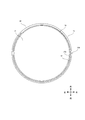
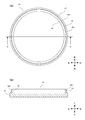
- FIG. 1A is a plan view of the film capacitor according to the first embodiment
- FIG. 1B is a cross-sectional view taken along line AA ′ of FIG.
- FIG. 2A is a plan view of the case main body according to the first embodiment
- FIG. 2B is a cross-sectional view taken along the line BB ′ of FIG.
- FIG. 3 is a bottom view of the case main body according to the first embodiment.
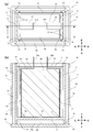
- FIG. 4A is a plan view of the lid according to the first embodiment
- FIG. 4B is a cross-sectional view taken along the line CC ′ of FIG. 4A.
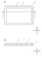
- FIG. 5 is a diagram illustrating a state in which the film capacitor is mounted on the printed board according to the first embodiment.
- FIG. 6A is a plan view of a film capacitor according to the second embodiment, and FIG. 6B is a cross-sectional view taken along the line DD ′ of FIG.
- FIG. 7A is a plan view of a case body according to the second embodiment, and FIG. 7B is a bottom view of the case body according to the second embodiment.
- FIG. 8A is a plan view of the lid according to the second embodiment, and FIG. 8B is a cross-sectional view taken along the line EE ′ of FIG. 8A.
- FIG. 9 is a diagram for explaining a film capacitor according to a modified example.
- 10A and 10B are diagrams for explaining a film capacitor according to a modification.
- the female screw portion 37 corresponds to the “first screw portion” recited in the claims.
- the male screw portion 43 corresponds to a “second screw portion” recited in the claims.
- FIG. 1 (a) is a plan view of a film capacitor 1A according to the first embodiment
- FIG. 1 (b) is a cross-sectional view taken along line AA ′ of FIG. 1 (a).
- 2A is a plan view of the case main body 30 according to the first embodiment
- FIG. 2B is a cross-sectional view taken along the line BB ′ of FIG. 2A.
- FIG. 3 is a bottom view of the case main body 30 according to the first embodiment.
- 4A is a plan view of the lid 40 according to the first embodiment
- FIG. 4B is a cross-sectional view taken along the line CC ′ of FIG. 4A.
- illustration of the filling resin 4 is omitted for the sake of convenience
- FIG. 1B the filling resin 4 is in a transparent state for convenience, and only the upper surface is drawn with diagonal lines. Yes.
- the film capacitor 1 ⁇ / b> A includes a capacitor element unit 2, a case 3, and a filling resin 4.
- the capacitor element unit 2 is accommodated in the case 3 and filled with the filling resin 4.
- the filling resin 4 is made of, for example, a thermosetting resin such as an epoxy resin, is injected into the case 3 in a molten state, and is cured when the case 3 is heated.
- the filling resin 4 covers most of the capacitor element unit 2 and protects these parts from moisture and impact.
- the capacitor element unit 2 includes a capacitor element 10 and a lead terminal portion 20 attached to the capacitor element 10.
- the capacitor element 10 is formed by stacking two metallized films on which aluminum is vapor-deposited on a dielectric film and winding the stacked metallized films, and has a substantially cylindrical shape.
- the capacitor element 10 is formed with a circular through hole 11 penetrating in the vertical direction at the center.
- the capacitor element 10 has a first electrode 12 formed on the upper end surface by spraying a metal such as zinc, and a second electrode 13 formed on the lower end surface by spraying a metal such as zinc. Is done.
- the capacitor element 10 may be formed of a metallized film in which other metal such as zinc or magnesium is vapor-deposited in addition to the metallized film in which aluminum is vapor-deposited on the dielectric film.
- condenser element 10 may be formed with the metallized film which vapor-deposited several metals among these metals, and may be formed with the metallized film vapor-deposited the alloy of these metals. .
- the lead terminal portion 20 includes a terminal mounting plate 21, a first terminal 22, a second terminal 23, a first lead wire 24, and a second lead wire 25.
- the terminal mounting plate 21 is made of a resin material and has a long plate shape in the left-right direction.
- the terminal mounting plate 21 is formed with a protruding portion 26 that protrudes downward, and the tip of the protruding portion 26 is fitted into the through hole 11 of the capacitor element 10.
- An insertion hole 27 that is connected to the through hole 11 is formed in the protrusion 26.
- the first terminal 22 and the second terminal 23 are made of a metal material having excellent conductivity, such as copper, and have a substantially L-shape.
- the first terminal 22 and the second terminal 23 are attached to both sides of the protrusion 26 on the terminal attachment plate 21.
- the first terminal 22 and the second terminal 23 protrude upward from the upper surface of the terminal mounting plate 21, and their base ends face the lower surface side of the terminal mounting plate 21.
- the first lead wire 24 electrically connects the first terminal 22 and the first electrode 12 of the capacitor element 10.
- the second lead wire 25 electrically connects the second terminal 23 and the second electrode 13 of the capacitor element 10.
- the second lead wire 25 is passed through the insertion hole 27 of the terminal mounting plate 21 and the through hole 11 of the capacitor element 10.
- Case 3 is a double-walled container having a bottomed cylindrical shape, and includes a case body 30 and a lid 40.
- the case body 30 and the lid portion 40 are formed of the same resin material having excellent moisture resistance and heat resistance, such as polyphenylene sulfide resin (PPS).
- PPS polyphenylene sulfide resin
- the case body 30 includes a circular bottom wall portion 31, a cylindrical inner wall portion 32 that rises from the peripheral edge of the bottom wall portion 31, a cylindrical outer wall portion 33 that surrounds the inner wall portion 32, an inner wall portion 32, and an outer wall portion 33. And a connecting portion 34 for connecting the two.
- the bottom wall portion 31 is formed with a recessed portion 31a that is slightly recessed on the lower surface thereof.
- a first receiving portion 35 and a second receiving portion 36 are formed on the left and right sides of the upper end portion 32a of the inner wall portion 32, respectively.
- the first receiving portion 35 and the second receiving portion 36 are each formed with three first claw portions 35a and second claw portions 36a.
- the outer wall portion 33 extends from the bottom wall portion 31 in a downward direction, that is, in a direction orthogonal to the bottom wall portion 31.
- the opening end portion 33 b of the outer wall portion 33 is located below the bottom wall portion 31.
- a female screw portion 37 is formed inside the open end portion 33b by a rib 37a that runs spirally.
- the connecting portion 34 is continuous over the entire circumference between the upper end portion 32a of the inner wall portion 32 (the end portion opposite to the bottom wall portion 31) and the upper end portion 33a of the outer wall portion 33 that faces the upper end portion 32a. They are connected to each other so that a gap S1 is formed between them.
- the lid portion 40 closes the opening surface 33 c of the outer wall portion 33 that faces the bottom wall portion 31 such that a gap S ⁇ b> 2 is formed between the lid portion 40 and the bottom wall portion 31.
- the lid 40 includes a disc-shaped lid body 41 and a fitting opening 42 having a flat cylindrical shape.
- the fitting opening 42 is formed on the upper surface of the lid main body 41.
- a male threaded portion 43 is formed on the peripheral wall surface 42a of the fitting opening 42 by a rib 43a that runs spirally.
- the fitting port portion 42 opens the opening end portion 33 b of the outer wall portion 33 while the lid body 41 is rotated so that the male screw portion 43 and the female screw portion 37 are engaged with each other. It will be inserted into.
- the fitting opening portion 42 is fitted to the end and the lid main body 41 comes into contact with the outer wall portion 33, the attachment of the lid portion 40 to the case main body 30 is completed, and the lid portion 40 is fixed to the case main body 30.
- the capacitor element unit 2 is held in a state of floating from the bottom wall portion 31 in the case 3 by the terminal mounting plate 21 being bridged between the first receiving portion 35 and the second receiving portion 36 of the inner wall portion 32. Is done.
- the upper surface of the filling resin 4 is located above the terminal mounting plate 21, and the capacitor element unit 2 is fixed in the case 3 by the hardened filling resin 4. Since both end portions of the terminal mounting plate 21 are pressed by the first claw portion 35a and the second claw portion 36a, the terminal mounting plate 21 is not easily pulled upward. In a state where the capacitor element unit 2 is accommodated in the case 3, the leading ends of the first terminal 22 and the second terminal 23 protrude to the outside of the case 3.
- FIG. 5 is a diagram illustrating a state in which the film capacitor 1 ⁇ / b> A according to the first embodiment is mounted on the printed circuit board 100.
- the film capacitor 1 ⁇ / b> A is directly mounted on the printed circuit board 100.
- Conductive patterns 101 and 102 corresponding to the first terminal 22 and the second terminal 23 of the film capacitor 1A are formed on the back surface of the printed circuit board 100, respectively.
- the first terminal 22 and the second terminal 23 are passed through the printed board 100 and electrically connected to the conductive patterns 101 and 102 by soldering.
- the case 3 is in a state where the opening side surface is in contact with the printed circuit board 100 and is covered with the printed circuit board 100.
- noise from the case 3 due to vibration of the capacitor element 10 has a gap (air layer) S ⁇ b> 2 in the upward direction. It is suppressed by the double wall structure of the bottom wall portion 31 and the lid portion 40, and is suppressed by the double wall structure of the inner wall portion 32 having the gap (air layer) S1 and the outer wall portion 33 in the front-rear and left-right directions.
- the In the downward direction the leakage of noise from the case 3 is suppressed because the layer of the filling resin 4 is thicker than the other portions and the opening portion of the case 3 is closed by the printed circuit board 100.
- the case 3 has a double wall structure including the inner wall portion 32 and the outer wall portion 33, and the bottom wall portion 31 and the lid portion 40, noise leakage caused by the vibration of the capacitor element 10 from the case 3 is suppressed. can do.
- the inner wall portion 32 and the outer wall portion 33 are integrally formed, the gap S1 between the inner wall portion 32 and the outer wall portion 33 does not fluctuate depending on the state of manufacturing work, and an expected gap S1 is secured. And a stable noise suppression effect is expected.
- the outer wall portion 33 is formed in a cylindrical shape and the lid portion 40 is fixed to the opening end portion 33b of the outer wall portion 33 by a screw method, it is easy to attach the lid portion 40 to the case body 30.
- the lid portion 40 can be firmly fixed to the case main body 30.
- FIG. 5 even after the film capacitor 1A is mounted on the printed circuit board 100, it is necessary to fill the gap S1 and the gap S2 of the case 3 with a sound absorbing material in order to further suppress noise leakage.
- the lid 40 can be easily removed from the case body 30 while being mounted on the printed circuit board 100, and the sound absorbing material can be filled.
- the case 3 has a configuration in which only the upper end portion 32a of the inner wall portion 32 and the upper end portion 33a of the outer wall portion 33 are connected by the connecting portion 34, the outer wall portion extends from the inner wall portion 32 via the connecting portion 34. It can be expected that the propagation of vibration (noise) to 33 can be reduced and the noise suppression effect is enhanced.
- FIG. 6A is a plan view of the film capacitor 1B according to the second embodiment, and FIG. 6B is a cross-sectional view taken along the line DD ′ of FIG. 6A.
- FIG. 7A is a plan view of the case main body 70 according to the second embodiment, and FIG. 7B is a bottom view of the case main body 70 according to the second embodiment.
- FIG. 8A is a plan view of the lid 80 according to the second embodiment, and FIG. 8B is a cross-sectional view taken along the line EE ′ of FIG. 8A.
- 6A the illustration of the filling resin 7 is omitted for the sake of convenience, and in FIG. 6B, the filling resin 7 is in a transparent state for the sake of convenience, and only the upper surface is drawn with diagonal lines. Yes.
- the film capacitor 1B includes a capacitor element unit 5, a case 6, and a filling resin 7.
- the capacitor element unit 5 is accommodated in the case 6 and filled with the filling resin 7.
- the filling resin 7 is made of, for example, a thermosetting resin such as an epoxy resin, like the filling resin 4 of the first embodiment, covers most of the capacitor element unit 5, and protects these parts from moisture and impact. .
- the capacitor element unit 5 includes a capacitor element 50 and a lead terminal portion 60 attached to the capacitor element 50.
- Capacitor element 50 is formed by stacking two metallized films on which aluminum is vapor-deposited on a dielectric film, winding or stacking the stacked metallized films, and pressing them flatly, and has a substantially long cross section. It has a columnar shape that forms a circle.
- a first electrode 51 is formed on the left end surface by spraying a metal such as zinc
- a second electrode 52 is formed on the right end surface similarly by spraying a metal such as zinc.
- the capacitor element 50 may be formed of a metallized film in which other metal such as zinc or magnesium is vapor-deposited in addition to the metallized film in which aluminum is vapor-deposited on the dielectric film.
- condenser element 50 may be formed with the metallized film which vapor-deposited several metals among these metals, and may be formed with the metallized film vapor-deposited the alloy of these metals. .
- the lead terminal portion 60 includes a first bus bar 61 and a second bus bar 62.
- the first bus bar 61 and the second bus bar 62 are formed by bending a metal plate having excellent conductivity, such as a copper plate, into a predetermined shape.
- the first bus bar 61 has a proximal end portion electrically connected to the first electrode 51 of the capacitor element 50 by a connection method such as soldering or welding, and has a first terminal 61a at the distal end portion.
- the second bus bar 62 has a proximal end portion electrically connected to the second electrode 52 of the capacitor element 50 by a connection method such as soldering or welding, and has a second terminal 62a at the distal end portion.
- the case 6 is a so-called double-walled container having a bottomed rectangular tube shape, and includes a case main body 70 and a lid 80.
- the case main body 70 and the lid 80 are made of the same resin material that is excellent in moisture resistance and heat resistance, such as PPS.
- the case body 70 includes a rectangular bottom wall 71, a square cylindrical inner wall 72 rising from the periphery of the bottom wall 71, a square cylindrical outer wall 73 surrounding the inner wall 72, an inner wall 72 and an outer wall
- the four connecting portions 74 that connect 73 are integrally formed.
- the bottom wall 71 has five disk-shaped protrusions 75 formed on the inner wall surface (upper surface), and the outer wall surface (lower surface) has a flat rectangular tube-shaped wall portion 76 along the peripheral edge. It is formed.
- a plurality of groove portions 77 extending in the vertical direction are formed on the left and right inner wall surfaces.
- the outer wall portion 73 extends from the bottom wall portion 71 in a downward direction, that is, in a direction orthogonal to the bottom wall portion 71.
- the positions of the lower end of the outer wall portion 73 and the lower end of the wall portion 76 are the same.
- Each of the four connecting portions 74 connects the corner portion of the inner wall portion 72 and the corner portion of the outer wall portion 73 facing the corner portion.
- the connecting portion 74 extends in the vertical direction from the upper end to the lower end of the outer wall portion 73.
- a gap S ⁇ b> 3 is formed between the inner wall portion 72 and the outer wall portion 73 connected by the connecting portion 74.
- the lid 80 closes the opening surface 73a of the outer wall 73 facing the bottom wall 71 so that a gap S4 is formed between the lid 80 and the bottom wall 71.
- the lid portion 40 includes a square plate-like lid body 81 and a fitting opening portion 82 formed on the upper surface of the lid body 81.
- the fitting opening 82 is formed in a flat rectangular tube shape in which portions corresponding to the four connecting portions 74 are interrupted.
- the thickness of the fitting opening portion 82 is slightly larger than the gap between the outer wall portion 73 and the wall portion 76.
- the lid 80 is fixed to the case main body 70 by press-fitting the fitting opening 82 into the gap between the outer wall 73 and the wall 76. At this time, in order to increase the fixing strength, an adhesive may be applied to each wall surface in contact with the outer wall portion 73 and the wall portion 76 of the fitting opening portion 82.
- the capacitor element unit 5 is supported by the projection 75 and held in a state slightly separated from the bottom wall 71.
- the upper surface of the filling resin 7 is located above the capacitor element 50, and the capacitor element unit 5 is fixed in the case 6 by the cured filling resin 7.
- the leading end portions of the first terminal 61 a of the first bus bar 61 and the second terminal 62 a of the second bus bar 62 protrude to the outside of the case 6.
- the film capacitor 1B of the present embodiment can also be directly mounted on a printed circuit board (not shown), like the film capacitor 1A of the first embodiment.
- the case 6 has a double wall structure including the inner wall portion 72 and the outer wall portion 73, and the bottom wall portion 71 and the lid portion 80, the leakage of noise caused by the vibration of the capacitor element 50 from the case 6 is suppressed. be able to.
- the inner wall portion 72 and the outer wall portion 73 are integrally formed, the gap S3 between the inner wall portion 72 and the outer wall portion 73 does not fluctuate depending on the state of the manufacturing work, and the desired gap S3 is secured. And a stable noise suppression effect is expected.
- the case 6 has a configuration in which a corner portion of the inner wall portion 72 and a corner portion of the outer wall portion 73 are connected by a connecting portion 74, and the corner portion of the inner wall portion 72 is a portion between two corner portions.
- the rigidity is higher than that of the capacitor element 50, and it is difficult to vibrate when the capacitor element 50 vibrates. Thereby, the propagation of vibration (noise) from the inner wall portion 72 to the outer wall portion 73 via the connecting portion 74 can be reduced, and it can be expected that the noise suppressing effect is enhanced.
- the gap S1 between the inner wall portion 32 and the outer wall portion 33 and the gap S2 between the bottom wall portion 31 and the lid portion 40 are air layers.
- the sound absorbing material 8 may be filled in the gaps S1 and S2.
- the sound absorbing material 8 a known sound absorbing material such as glass wool, rock wool, felt or the like can be used. Thereby, it is expected that noise leakage from the case 3 is further suppressed.
- the sound absorbing material may be filled in the gap S3 between the inner wall portion 72 and the outer wall portion 73 and the gap S2 between the bottom wall portion 71 and the lid portion 80.
- the connecting portion 34 is continuously provided over the entire circumference between the upper end portion 32a of the inner wall portion 32 and the upper end portion 33a of the outer wall portion 33.
- the connecting portion 34 may be provided intermittently over the entire circumference between the upper end portion 32 a of the inner wall portion 32 and the upper end portion 33 a of the outer wall portion 33. In this case, it is desirable from the viewpoint of strength that the connecting portion 34 is present in the portion of the inner wall portion 32 where the first receiving portion 35 and the second receiving portion 36 are formed.
- the corner portion of the inner wall portion 72 and the corner portion of the outer wall portion 73 are connected by the connecting portion 74.
- the position of the connecting portion 74 may not be the position of the corner portion.
- the connecting portion 74 is located at the center position between the corner portions. Also good.
- the case main body 30 and the lid portion 40 may be fixed by a press-fitting method in the same manner as the film capacitor 1B of the second embodiment instead of the screw method.
- the inner wall portion 32 and the outer wall portion 33 may be connected by a connecting portion extending in the vertical direction.
- a connecting portion such as the film capacitor 1B of the second embodiment is provided. I can't.
- the connecting portion is continuously provided over the entire circumference between the upper end portion of the inner wall portion 72 and the upper end portion of the outer wall portion 73.
- the provided structure may be taken.
- the capacitor element units 2 and 5 are configured by one capacitor element 10 and 50.
- the present invention is not limited to this, and the capacitor element units 2 and 5 may be configured by a plurality of capacitor elements 10 and 50.
- the capacitor elements 10 and 50 are formed by stacking two metallized films obtained by vapor-depositing aluminum on a dielectric film and winding the stacked metallized films.
- the capacitor elements 10 and 50 are formed by stacking a metallized film in which aluminum is vapor-deposited on both sides of the dielectric film and an insulating film, and winding the dielectric film. May be formed.
- condenser 1A, 1B was mentioned as an example of the capacitor
- the present invention can also be applied to capacitors other than the film capacitors 1A and 1B.
- the terms indicating directions such as “upward” and “downward” indicate relative directions that depend only on the relative positional relationship of the constituent members, and include vertical and horizontal directions. It does not indicate the absolute direction.
- the present invention is useful for capacitors used in various electronic equipment, electrical equipment, industrial equipment, vehicle electrical equipment, and the like.
Abstract
This film capacitor (1A) is provided with: a capacitor element (10); a case (3) in which the capacitor element (10) is accommodated; and a filling resin (4) for filling the inside of the case (3). The case (3) includes a case main body (30) and a cover part (40). The case main body (30) is provided by integrally forming: a bottom wall portion (31); a cylindrical inner wall portion (32) which protrudes upward from a peripheral edge of the bottom wall portion (31); a cylindrical outer wall portion (33) which surrounds the inner wall portion (32) and extends, further than the bottom wall portion (31), in a direction perpendicular to the bottom wall portion (31); and a connecting portion (34) that connects the inner wall portion (32) and the outer wall portion (33) so as to create a gap (S1) between both the wall portions. The cover part (40) covers an opening area (33c) of the outer wall portion (33) so as to form a gap (S2) between the bottom wall portion (31) and the cover part (40), the opening area (33c) facing the bottom wall portion (31).
Description
本発明は、コンデンサに関する。
The present invention relates to a capacitor.
従来、バスバーが接続されたコンデンサ素子を、上面が開口するケース内に収納し、当該ケース内にエポキシ樹脂などの充填樹脂を充填するようにしたケースモールド型のコンデンサが知られている。
Conventionally, a case mold type capacitor is known in which a capacitor element to which a bus bar is connected is housed in a case having an upper surface opened, and a filling resin such as an epoxy resin is filled in the case.
かかるコンデンサでは、コンデンサ素子に交流電圧が印加された際、コンデンサ素子が振動しやすく、この振動に起因する騒音が発生しやすい。そこで、ケースの外部に漏れる騒音を抑制するために、ケースの側面(周面)および底面が、互いの間に隙間を有する2つの壁部により構成され得る。
In such a capacitor, when an AC voltage is applied to the capacitor element, the capacitor element is likely to vibrate, and noise due to this vibration is likely to occur. Therefore, in order to suppress noise leaking to the outside of the case, the side surface (circumferential surface) and the bottom surface of the case can be configured by two wall portions having a gap between each other.
このようにケースの側面と底面とが二重の壁構造とされる場合、ケースを1つ部材で作成することが難しい。よって、通常は、2つの部材を結合することによりケースが作成され得る。
If the side and bottom of the case have a double wall structure, it is difficult to create a case with one member. Thus, a case can usually be created by joining two members.
特許文献1には、樹脂製の内装ケースと、当該内装ケースを収容する金属製の外装ケースとによりケースを構成するようにしたケースモールド型のコンデンサが記載されている。内装ケースの側面上部には、外側に突出するように結合部が設けられる。一方、外装ケースの側面上部には、凹み形状を有する結合部が設けられ、当該結合部に内装ケースの結合部が上方から嵌め込まれる。双方の結合部をボルト等で止めることにより、内装ケースと外装ケースとが結合されて一体となる。
Patent Document 1 describes a case mold type capacitor in which a case is constituted by a resin interior case and a metal exterior case that accommodates the interior case. A coupling portion is provided on the upper side of the inner case so as to protrude outward. On the other hand, a coupling portion having a concave shape is provided on the upper side surface of the exterior case, and the coupling portion of the interior case is fitted into the coupling portion from above. The inner case and the outer case are combined and integrated by fastening both connecting portions with bolts or the like.
特許文献1のようにケースを構成する場合、双方の結合部の嵌め込み寸法の精度や、双方の結合部に形成されるボルトのための孔の寸法精度をあまり厳しくすると、双方の結合部同士が嵌り込みにくくなったり、双方の孔の位置がずれたときにボルトが止まりにくくなったりしやすい。そこで、内装ケースと外装ケースとを結合しやすくするためには、双方の結合部の間に、ある程度の前後左右方向の遊びが設けられるとよく、また、内装ケースの結合部の孔が外装ケースの孔より大きくされるとよい。
When configuring the case as in Patent Document 1, if the accuracy of the fitting dimensions of both coupling parts and the dimensional accuracy of the holes for the bolts formed in both coupling parts are too strict, It is difficult to fit the bolt or the bolt is difficult to stop when the positions of both holes are shifted. Therefore, in order to facilitate the coupling of the interior case and the exterior case, it is preferable that a certain amount of play in the front / rear and left / right directions is provided between the coupling portions of the two, and the holes in the coupling portion of the interior case are provided in the exterior case. It should be larger than the hole.
しかしながら、こうした場合、ケースを作成する際に、外装ケースに対して内装ケースが所期の位置から前後左右方向にずれやすくなり、内装ケースの側面が外装ケースの側面に寄った部分で隙間が小さくなりやすい。これにより、ケースの側面方向(周面方向)において、隙間にばらつきが生じることで、安定した騒音抑制効果が得られにくくなることが懸念される。
However, in such a case, when creating the case, the inner case is likely to be displaced from the intended position in the front-rear and left-right directions with respect to the outer case, and the gap is small at the portion where the side surface of the inner case is close to the side surface of the outer case. Prone. Thereby, there is a concern that a variation in the gap in the side surface direction (circumferential surface direction) of the case makes it difficult to obtain a stable noise suppression effect.
かかる課題に鑑み、本発明は、二重の壁構造のケースによる騒音の抑制効果を良好に得ることが期待できるコンデンサを提供することを目的とする。
In view of such a problem, an object of the present invention is to provide a capacitor that can be expected to obtain a satisfactory noise suppression effect by a case of a double wall structure.
本発明の主たる態様に係るコンデンサは、コンデンサ素子と、前記コンデンサ素子が収容されるケースと、前記ケース内に充填される充填樹脂と、を備える。ここで、前記ケースは、底壁部と、当該底壁部の周縁から立ち上がる筒状の内壁部と、当該内壁部を囲み前記底壁部と直交する方向に前記底壁部よりも延びる筒状の外壁部と、前記内壁部と前記外壁部とを双方の壁部の間に隙間が生じるように連結する連結部と、が一体に形成されてなるケース本体と、前記外壁部における前記底壁部に対向する開口面を、前記底壁部との間に隙間が形成されるように塞ぐ蓋部と、を含む。
A capacitor according to a main aspect of the present invention includes a capacitor element, a case in which the capacitor element is accommodated, and a filling resin filled in the case. Here, the case includes a bottom wall portion, a cylindrical inner wall portion that rises from the periphery of the bottom wall portion, and a cylindrical shape that surrounds the inner wall portion and extends in a direction orthogonal to the bottom wall portion. A case main body formed integrally with the outer wall portion, and a connecting portion that connects the inner wall portion and the outer wall portion so as to create a gap between the two wall portions, and the bottom wall of the outer wall portion A lid portion that closes an opening surface facing the portion so as to form a gap with the bottom wall portion.
本発明によれば、二重の壁構造のケースによる騒音の抑制効果を良好に得ることが期待できる。
According to the present invention, it can be expected that the noise suppression effect by the case of the double wall structure is obtained.
本発明の効果ないし意義は、以下に示す実施の形態の説明により更に明らかとなろう。ただし、以下に示す実施の形態は、あくまでも、本発明を実施化する際の一つの例示であって、本発明は、以下の実施の形態に記載されたものに何ら制限されるものではない。
The effect or significance of the present invention will become more apparent from the following description of embodiments. However, the embodiment described below is merely an example when the present invention is implemented, and the present invention is not limited to what is described in the following embodiment.
以下、本発明のコンデンサの一実施形態であるフィルムコンデンサについて図を参照して説明する。便宜上、各図には、適宜、前後、左右および上下の方向が付記されている。なお、図示の方向は、あくまでフィルムコンデンサの相対的な方向を示すものであり、絶対的な方向を示すものではない。
Hereinafter, a film capacitor which is an embodiment of the capacitor of the present invention will be described with reference to the drawings. For convenience, front and rear, left and right, and up and down directions are appropriately appended to each drawing. In addition, the direction of illustration shows the relative direction of a film capacitor to the last, and does not show an absolute direction.
<第1実施形態>
以下、第1実施形態に係る、フィルムコンデンサ1Aについて説明する。 <First Embodiment>
Hereinafter, thefilm capacitor 1 </ b> A according to the first embodiment will be described.
以下、第1実施形態に係る、フィルムコンデンサ1Aについて説明する。 <First Embodiment>
Hereinafter, the
本実施の形態において、雌ネジ部37が、特許請求の範囲に記載の「第1のネジ部」に対応する。また、雄ネジ部43が、特許請求の範囲に記載の「第2のネジ部」に対応する。
In the present embodiment, the female screw portion 37 corresponds to the “first screw portion” recited in the claims. The male screw portion 43 corresponds to a “second screw portion” recited in the claims.
ただし、上記記載は、あくまで、特許請求の範囲の構成と実施形態の構成とを対応付けることを目的とするものであって、上記対応付けによって特許請求の範囲に記載の発明が実施形態の構成に何ら限定されるものではない。
However, the above description is only for the purpose of associating the configuration of the claims with the configuration of the embodiment, and the invention described in the claims is incorporated into the configuration of the embodiment by the above association. It is not limited at all.
図1(a)は、第1実施形態に係る、フィルムコンデンサ1Aの平面図であり、図1(b)は、図1(a)のA-A´断面図である。図2(a)は、第1実施形態に係る、ケース本体30の平面図であり、図2(b)は、図2(a)のB-B´断面図である。図3は、第1実施形態に係る、ケース本体30の底面図である。図4(a)は、第1実施形態に係る、蓋部40の平面図であり、図4(b)は、図4(a)のC-C´断面図である。なお、図1(a)では、便宜上、充填樹脂4の図示が省略されており、図1(b)では、便宜上、充填樹脂4が透明な状態とされ、その上面のみが斜線で描かれている。
FIG. 1 (a) is a plan view of a film capacitor 1A according to the first embodiment, and FIG. 1 (b) is a cross-sectional view taken along line AA ′ of FIG. 1 (a). 2A is a plan view of the case main body 30 according to the first embodiment, and FIG. 2B is a cross-sectional view taken along the line BB ′ of FIG. 2A. FIG. 3 is a bottom view of the case main body 30 according to the first embodiment. 4A is a plan view of the lid 40 according to the first embodiment, and FIG. 4B is a cross-sectional view taken along the line CC ′ of FIG. 4A. In FIG. 1A, illustration of the filling resin 4 is omitted for the sake of convenience, and in FIG. 1B, the filling resin 4 is in a transparent state for convenience, and only the upper surface is drawn with diagonal lines. Yes.
フィルムコンデンサ1Aは、コンデンサ素子ユニット2と、ケース3と、充填樹脂4とを含む。ケース3内に、コンデンサ素子ユニット2が収容され、充填樹脂4が充填される。充填樹脂4は、たとえば、エポキシ樹脂等の熱硬化性樹脂からなり、溶融状態でケース3内に注入され、ケース3が加熱されることにより硬化する。充填樹脂4は、コンデンサ素子ユニット2の大部分を覆い、これらの部分を湿気や衝撃から保護する。
The film capacitor 1 </ b> A includes a capacitor element unit 2, a case 3, and a filling resin 4. The capacitor element unit 2 is accommodated in the case 3 and filled with the filling resin 4. The filling resin 4 is made of, for example, a thermosetting resin such as an epoxy resin, is injected into the case 3 in a molten state, and is cured when the case 3 is heated. The filling resin 4 covers most of the capacitor element unit 2 and protects these parts from moisture and impact.
コンデンサ素子ユニット2は、コンデンサ素子10と、コンデンサ素子10に取り付けられる引き出し端子部20とを含む。コンデンサ素子10は、誘電体フィルム上にアルミニウムを蒸着させた2枚の金属化フィルムを重ね、重ねた金属化フィルムを巻回することにより形成され、ほぼ円柱形状を有する。コンデンサ素子10には、中央部に、上下方向に貫通する円形の貫通孔11が形成される。また、コンデンサ素子10には、上側の端面に、亜鉛等の金属の吹付けにより第1電極12が形成され、下側の端面に、同じく亜鉛等の金属の吹付けにより第2電極13が形成される。
The capacitor element unit 2 includes a capacitor element 10 and a lead terminal portion 20 attached to the capacitor element 10. The capacitor element 10 is formed by stacking two metallized films on which aluminum is vapor-deposited on a dielectric film and winding the stacked metallized films, and has a substantially cylindrical shape. The capacitor element 10 is formed with a circular through hole 11 penetrating in the vertical direction at the center. The capacitor element 10 has a first electrode 12 formed on the upper end surface by spraying a metal such as zinc, and a second electrode 13 formed on the lower end surface by spraying a metal such as zinc. Is done.
なお、コンデンサ素子10は、誘電体フィルム上にアルミニウムを蒸着させた金属化フィルム以外にも、亜鉛、マグネシウム等の他の金属を蒸着させた金属化フィルムにより形成されてもよい。あるいは、コンデンサ素子10は、これらの金属のうち、複数の金属を蒸着させた金属化フィルムにより形成されてもよいし、これらの金属どうしの合金を蒸着させた金属化フィルムにより形成されてもよい。
The capacitor element 10 may be formed of a metallized film in which other metal such as zinc or magnesium is vapor-deposited in addition to the metallized film in which aluminum is vapor-deposited on the dielectric film. Or the capacitor | condenser element 10 may be formed with the metallized film which vapor-deposited several metals among these metals, and may be formed with the metallized film vapor-deposited the alloy of these metals. .
引き出し端子部20は、端子取付板21と、第1端子22と、第2端子23と、第1リード線24と、第2リード線25とを含む。端子取付板21は、樹脂材料により形成され、左右方向に長い板状を有する。端子取付板21には、下方に突出する突起部26が形成され、この突起部26の先端部がコンデンサ素子10の貫通孔11に嵌め込まれる。突起部26には、貫通孔11に繋がる挿通孔27が形成される。
The lead terminal portion 20 includes a terminal mounting plate 21, a first terminal 22, a second terminal 23, a first lead wire 24, and a second lead wire 25. The terminal mounting plate 21 is made of a resin material and has a long plate shape in the left-right direction. The terminal mounting plate 21 is formed with a protruding portion 26 that protrudes downward, and the tip of the protruding portion 26 is fitted into the through hole 11 of the capacitor element 10. An insertion hole 27 that is connected to the through hole 11 is formed in the protrusion 26.
第1端子22および第2端子23は、銅等の導電性に優れる金属材料により形成され、ほぼL字形を有する。第1端子22および第2端子23は、端子取付板21において、突起部26の両側に取り付けられる。第1端子22および第2端子23は、端子取付板21の上面から上方に突き出し、その基端部が端子取付板21の下面側に臨む。
The first terminal 22 and the second terminal 23 are made of a metal material having excellent conductivity, such as copper, and have a substantially L-shape. The first terminal 22 and the second terminal 23 are attached to both sides of the protrusion 26 on the terminal attachment plate 21. The first terminal 22 and the second terminal 23 protrude upward from the upper surface of the terminal mounting plate 21, and their base ends face the lower surface side of the terminal mounting plate 21.
第1リード線24は、第1端子22とコンデンサ素子10の第1電極12とを電気的に接続する。第2リード線25は、第2端子23とコンデンサ素子10の第2電極13とを電気的に接続する。第2端子23と第2電極13との間を接続するため、第2リード線25は、端子取付板21の挿通孔27とコンデンサ素子10の貫通孔11とを通される。第1リード線24と、第1端子22および第1電極12との接続方法、および、第2リード線25と第2端子23および第2電極13との接続方法として、たとえば、半田付や溶接を挙げることができる。
The first lead wire 24 electrically connects the first terminal 22 and the first electrode 12 of the capacitor element 10. The second lead wire 25 electrically connects the second terminal 23 and the second electrode 13 of the capacitor element 10. In order to connect between the second terminal 23 and the second electrode 13, the second lead wire 25 is passed through the insertion hole 27 of the terminal mounting plate 21 and the through hole 11 of the capacitor element 10. As a method for connecting the first lead wire 24 to the first terminal 22 and the first electrode 12 and a method for connecting the second lead wire 25 to the second terminal 23 and the second electrode 13, for example, soldering or welding Can be mentioned.
ケース3は、有底の円筒形状を有する、二重の壁構造の容器であり、ケース本体30と、蓋部40とを含む。ケース本体30および蓋部40は、ポリフェニレンサルファイド樹脂(PPS)等、耐湿性および耐熱性に優れる同じ樹脂材料により形成される。
Case 3 is a double-walled container having a bottomed cylindrical shape, and includes a case body 30 and a lid 40. The case body 30 and the lid portion 40 are formed of the same resin material having excellent moisture resistance and heat resistance, such as polyphenylene sulfide resin (PPS).
ケース本体30は、円形の底壁部31と、底壁部31の周縁から立ち上がる円筒状の内壁部32と、内壁部32を囲む円筒状の外壁部33と、内壁部32と外壁部33とを連結する連結部34と、が一体に形成されてなる。底壁部31には、その下面に、僅かに窪む凹み部31aが形成される。
The case body 30 includes a circular bottom wall portion 31, a cylindrical inner wall portion 32 that rises from the peripheral edge of the bottom wall portion 31, a cylindrical outer wall portion 33 that surrounds the inner wall portion 32, an inner wall portion 32, and an outer wall portion 33. And a connecting portion 34 for connecting the two. The bottom wall portion 31 is formed with a recessed portion 31a that is slightly recessed on the lower surface thereof.
内壁部32の上端部32aには、左側と右側に、それぞれ、第1受け部35と第2受け部36とが形成される。第1受け部35と第2受け部36には、それぞれ、3つの第1爪部35aおよび第2爪部36aが形成される。
A first receiving portion 35 and a second receiving portion 36 are formed on the left and right sides of the upper end portion 32a of the inner wall portion 32, respectively. The first receiving portion 35 and the second receiving portion 36 are each formed with three first claw portions 35a and second claw portions 36a.
外壁部33は、下方向、即ち底壁部31と直交する方向に底壁部31よりも延びる。外壁部33の開口端部33bは、底壁部31よりも下に位置する。開口端部33bの内側には、螺旋状に走るリブ37aによって雌ネジ部37が形成される。連結部34は、内壁部32の上端部32a(底壁部31とは反対側の端部)と、上端部32aに対向する外壁部33の上端部33aとの間に全周に亘って連続的に設けられ、これらの間に隙間S1が形成されるように、これらの間を連結する。
The outer wall portion 33 extends from the bottom wall portion 31 in a downward direction, that is, in a direction orthogonal to the bottom wall portion 31. The opening end portion 33 b of the outer wall portion 33 is located below the bottom wall portion 31. A female screw portion 37 is formed inside the open end portion 33b by a rib 37a that runs spirally. The connecting portion 34 is continuous over the entire circumference between the upper end portion 32a of the inner wall portion 32 (the end portion opposite to the bottom wall portion 31) and the upper end portion 33a of the outer wall portion 33 that faces the upper end portion 32a. They are connected to each other so that a gap S1 is formed between them.
蓋部40は、外壁部33における底壁部31に対向する開口面33cを、底壁部31との間に隙間S2が形成されるように塞ぐ。蓋部40は、円盤状の蓋本体41と、扁平な円筒状を有する嵌込み口部42とを含む。嵌込み口部42は、蓋本体41の上面に形成される。嵌込み口部42の周壁面42aには、螺旋状に走るリブ43aによって雄ネジ部43が形成される。
The lid portion 40 closes the opening surface 33 c of the outer wall portion 33 that faces the bottom wall portion 31 such that a gap S <b> 2 is formed between the lid portion 40 and the bottom wall portion 31. The lid 40 includes a disc-shaped lid body 41 and a fitting opening 42 having a flat cylindrical shape. The fitting opening 42 is formed on the upper surface of the lid main body 41. A male threaded portion 43 is formed on the peripheral wall surface 42a of the fitting opening 42 by a rib 43a that runs spirally.
ケース本体30に蓋部40が取り付けられる際には、雄ネジ部43と雌ネジ部37とが噛み合うように、蓋本体41が回転されながら嵌込み口部42が外壁部33の開口端部33bに嵌め込まれていく。嵌込み口部42が最後まで嵌め込まれ、蓋本体41が外壁部33に当接すると、ケース本体30への蓋部40の取り付けが完了し、蓋部40がケース本体30に固定される。
When the lid portion 40 is attached to the case body 30, the fitting port portion 42 opens the opening end portion 33 b of the outer wall portion 33 while the lid body 41 is rotated so that the male screw portion 43 and the female screw portion 37 are engaged with each other. It will be inserted into. When the fitting opening portion 42 is fitted to the end and the lid main body 41 comes into contact with the outer wall portion 33, the attachment of the lid portion 40 to the case main body 30 is completed, and the lid portion 40 is fixed to the case main body 30.
コンデンサ素子ユニット2は、内壁部32の第1受け部35と第2受け部36との間に端子取付板21が架け渡されることによって、ケース3内において底壁部31から浮いた状態に保持される。充填樹脂4の上面は、端子取付板21より上に位置し、硬化した充填樹脂4によってコンデンサ素子ユニット2がケース3内で固定される。端子取付板21の両端部が第1爪部35aおよび第2爪部36aで押さえられるため、端子取付板21が上方に抜けにくい。コンデンサ素子ユニット2が、ケース3内に収容された状態において、第1端子22および第2端子23の先端部がケース3の外側へ張り出す。
The capacitor element unit 2 is held in a state of floating from the bottom wall portion 31 in the case 3 by the terminal mounting plate 21 being bridged between the first receiving portion 35 and the second receiving portion 36 of the inner wall portion 32. Is done. The upper surface of the filling resin 4 is located above the terminal mounting plate 21, and the capacitor element unit 2 is fixed in the case 3 by the hardened filling resin 4. Since both end portions of the terminal mounting plate 21 are pressed by the first claw portion 35a and the second claw portion 36a, the terminal mounting plate 21 is not easily pulled upward. In a state where the capacitor element unit 2 is accommodated in the case 3, the leading ends of the first terminal 22 and the second terminal 23 protrude to the outside of the case 3.
図5は、第1実施形態に係る、フィルムコンデンサ1Aがプリント基板100に実装された状態を示す図である。
FIG. 5 is a diagram illustrating a state in which the film capacitor 1 </ b> A according to the first embodiment is mounted on the printed circuit board 100.
図5に示すように、フィルムコンデンサ1Aは、プリント基板100に直接、実装される。プリント基板100には、裏面に、フィルムコンデンサ1Aの第1端子22および第2端子23にそれぞれ対応する導電パターン101、102が形成される。第1端子22および第2端子23がプリント基板100を通され、導電パターン101、102に半田付けにより電気的に接続される。ケース3は、開口側の面がプリント基板100に接触してプリント基板100で覆われた状態となる。
As shown in FIG. 5, the film capacitor 1 </ b> A is directly mounted on the printed circuit board 100. Conductive patterns 101 and 102 corresponding to the first terminal 22 and the second terminal 23 of the film capacitor 1A are formed on the back surface of the printed circuit board 100, respectively. The first terminal 22 and the second terminal 23 are passed through the printed board 100 and electrically connected to the conductive patterns 101 and 102 by soldering. The case 3 is in a state where the opening side surface is in contact with the printed circuit board 100 and is covered with the printed circuit board 100.
図5のように、フィルムコンデンサ1Aがプリント基板100に実装された状態において、コンデンサ素子10の振動に起因する騒音のケース3からの漏れは、上方向については、隙間(空気層)S2を有する底壁部31と蓋部40との二重の壁構造によって抑制され、前後左右方向については、隙間(空気層)S1を有する内壁部32と外壁部33との二重の壁構造によって抑制される。下方向については、充填樹脂4の層が他の部分よりも厚いこと、および、ケース3の開口部分がプリント基板100で閉鎖されていることにより、ケース3からの騒音の漏れが抑制される。
As shown in FIG. 5, in the state where the film capacitor 1 </ b> A is mounted on the printed circuit board 100, noise from the case 3 due to vibration of the capacitor element 10 has a gap (air layer) S <b> 2 in the upward direction. It is suppressed by the double wall structure of the bottom wall portion 31 and the lid portion 40, and is suppressed by the double wall structure of the inner wall portion 32 having the gap (air layer) S1 and the outer wall portion 33 in the front-rear and left-right directions. The In the downward direction, the leakage of noise from the case 3 is suppressed because the layer of the filling resin 4 is thicker than the other portions and the opening portion of the case 3 is closed by the printed circuit board 100.
<実施の形態の効果>
以上、本実施の形態によれば、以下の効果が奏される。 <Effect of Embodiment>
As described above, according to the present embodiment, the following effects are exhibited.
以上、本実施の形態によれば、以下の効果が奏される。 <Effect of Embodiment>
As described above, according to the present embodiment, the following effects are exhibited.
ケース3が、内壁部32と外壁部33および底壁部31と蓋部40からなる二重の壁構造とされているので、ケース3からのコンデンサ素子10の振動に起因する騒音の漏れを抑制することができる。しかも、内壁部32と外壁部33とが一体形成されているため、製造作業の具合によって内壁部32と外壁部33との隙間S1が変動するようなことがなく、所期の隙間S1を確保でき、安定した騒音抑制効果が期待される。
Since the case 3 has a double wall structure including the inner wall portion 32 and the outer wall portion 33, and the bottom wall portion 31 and the lid portion 40, noise leakage caused by the vibration of the capacitor element 10 from the case 3 is suppressed. can do. In addition, since the inner wall portion 32 and the outer wall portion 33 are integrally formed, the gap S1 between the inner wall portion 32 and the outer wall portion 33 does not fluctuate depending on the state of manufacturing work, and an expected gap S1 is secured. And a stable noise suppression effect is expected.
また、外壁部33が円筒形状に形成され、外壁部33の開口端部33bへの蓋部40の固定がネジ方式で行われるようにしたので、蓋部40のケース本体30への取り付けが容易であり、且つ、蓋部40をケース本体30に強固に固定できる。さらに、図5のように、フィルムコンデンサ1Aがプリント基板100に実装された後、騒音の漏れを一層抑制するために、ケース3の隙間S1および隙間S2に吸音材を充填する必要が生じても、プリント基板100への実装状態のまま、ケース本体30から蓋部40を容易に外して吸音材の充填を行うことが可能となる。
Further, since the outer wall portion 33 is formed in a cylindrical shape and the lid portion 40 is fixed to the opening end portion 33b of the outer wall portion 33 by a screw method, it is easy to attach the lid portion 40 to the case body 30. In addition, the lid portion 40 can be firmly fixed to the case main body 30. Further, as shown in FIG. 5, even after the film capacitor 1A is mounted on the printed circuit board 100, it is necessary to fill the gap S1 and the gap S2 of the case 3 with a sound absorbing material in order to further suppress noise leakage. The lid 40 can be easily removed from the case body 30 while being mounted on the printed circuit board 100, and the sound absorbing material can be filled.
さらに、ケース3は、内壁部32の上端部32aと外壁部33の上端部33aとの間のみが連結部34で連結される構成であるため、連結部34を介した内壁部32から外壁部33への振動(騒音)の伝播を小さくでき、騒音の抑制効果が高まることが期待できる。
Furthermore, since the case 3 has a configuration in which only the upper end portion 32a of the inner wall portion 32 and the upper end portion 33a of the outer wall portion 33 are connected by the connecting portion 34, the outer wall portion extends from the inner wall portion 32 via the connecting portion 34. It can be expected that the propagation of vibration (noise) to 33 can be reduced and the noise suppression effect is enhanced.
<第2実施形態>
以下、第2実施形態に係る、フィルムコンデンサ1Bについて説明する。 Second Embodiment
Hereinafter, thefilm capacitor 1B according to the second embodiment will be described.
以下、第2実施形態に係る、フィルムコンデンサ1Bについて説明する。 Second Embodiment
Hereinafter, the
図6(a)は、第2実施形態に係る、フィルムコンデンサ1Bの平面図であり、図6(b)は、図6(a)のD-D´断面図である。図7(a)は、第2実施形態に係る、ケース本体70の平面図であり、図7(b)は、第2実施形態に係る、ケース本体70の底面図である。図8(a)は、第2実施形態に係る、蓋部80の平面図であり、図8(b)は、図8(a)のE-E´断面図である。なお、図6(a)では、便宜上、充填樹脂7の図示が省略されており、図6(b)では、便宜上、充填樹脂7が透明な状態とされ、その上面のみが斜線で描かれている。
FIG. 6A is a plan view of the film capacitor 1B according to the second embodiment, and FIG. 6B is a cross-sectional view taken along the line DD ′ of FIG. 6A. FIG. 7A is a plan view of the case main body 70 according to the second embodiment, and FIG. 7B is a bottom view of the case main body 70 according to the second embodiment. FIG. 8A is a plan view of the lid 80 according to the second embodiment, and FIG. 8B is a cross-sectional view taken along the line EE ′ of FIG. 8A. 6A, the illustration of the filling resin 7 is omitted for the sake of convenience, and in FIG. 6B, the filling resin 7 is in a transparent state for the sake of convenience, and only the upper surface is drawn with diagonal lines. Yes.
フィルムコンデンサ1Bは、コンデンサ素子ユニット5と、ケース6と、充填樹脂7とを含む。ケース6内に、コンデンサ素子ユニット5が収容され、充填樹脂7が充填される。充填樹脂7は、上記第1実施形態の充填樹脂4と同様、たとえば、エポキシ樹脂等の熱硬化性樹脂からなり、コンデンサ素子ユニット5の大部分を覆い、これらの部分を湿気や衝撃から保護する。
The film capacitor 1B includes a capacitor element unit 5, a case 6, and a filling resin 7. The capacitor element unit 5 is accommodated in the case 6 and filled with the filling resin 7. The filling resin 7 is made of, for example, a thermosetting resin such as an epoxy resin, like the filling resin 4 of the first embodiment, covers most of the capacitor element unit 5, and protects these parts from moisture and impact. .
コンデンサ素子ユニット5は、コンデンサ素子50と、コンデンサ素子50に取り付けられる引き出し端子部60とを含む。コンデンサ素子50は、誘電体フィルム上にアルミニウムを蒸着させた2枚の金属化フィルムを重ね、重ねた金属化フィルムを巻回または積層し、扁平状に押圧することにより形成され、断面がほぼ長円となる柱体形状を有する。コンデンサ素子50には、左側の端面に、亜鉛等の金属の吹付けにより第1電極51が形成され、右側の端面に、同じく亜鉛等の金属の吹付けにより第2電極52が形成される。
The capacitor element unit 5 includes a capacitor element 50 and a lead terminal portion 60 attached to the capacitor element 50. Capacitor element 50 is formed by stacking two metallized films on which aluminum is vapor-deposited on a dielectric film, winding or stacking the stacked metallized films, and pressing them flatly, and has a substantially long cross section. It has a columnar shape that forms a circle. In the capacitor element 50, a first electrode 51 is formed on the left end surface by spraying a metal such as zinc, and a second electrode 52 is formed on the right end surface similarly by spraying a metal such as zinc.
なお、コンデンサ素子50は、誘電体フィルム上にアルミニウムを蒸着させた金属化フィルム以外にも、亜鉛、マグネシウム等の他の金属を蒸着させた金属化フィルムにより形成されてもよい。あるいは、コンデンサ素子50は、これらの金属のうち、複数の金属を蒸着させた金属化フィルムにより形成されてもよいし、これらの金属どうしの合金を蒸着させた金属化フィルムにより形成されてもよい。
The capacitor element 50 may be formed of a metallized film in which other metal such as zinc or magnesium is vapor-deposited in addition to the metallized film in which aluminum is vapor-deposited on the dielectric film. Or the capacitor | condenser element 50 may be formed with the metallized film which vapor-deposited several metals among these metals, and may be formed with the metallized film vapor-deposited the alloy of these metals. .
引き出し端子部60は、第1バスバー61と、第2バスバー62とを含む。第1バスバー61および第2バスバー62は、銅板等の導電性に優れる金属板を、所定の形状に折り曲げることにより形成される。第1バスバー61は、基端部がコンデンサ素子50の第1電極51に半田付け、溶接等の接続方法により電気的に接続され、先端部に第1端子61aを有する。第2バスバー62は、基端部がコンデンサ素子50の第2電極52に半田付け、溶接等の接続方法により電気的に接続され、先端部に第2端子62aを有する。
The lead terminal portion 60 includes a first bus bar 61 and a second bus bar 62. The first bus bar 61 and the second bus bar 62 are formed by bending a metal plate having excellent conductivity, such as a copper plate, into a predetermined shape. The first bus bar 61 has a proximal end portion electrically connected to the first electrode 51 of the capacitor element 50 by a connection method such as soldering or welding, and has a first terminal 61a at the distal end portion. The second bus bar 62 has a proximal end portion electrically connected to the second electrode 52 of the capacitor element 50 by a connection method such as soldering or welding, and has a second terminal 62a at the distal end portion.
ケース6は、有底の四角筒形状を有する、いわゆる二重の壁構造の容器であり、ケース本体70と、蓋部80とを含む。ケース本体70および蓋部80は、PPS等、耐湿性および耐熱性に優れる同じ樹脂材料により形成される。
The case 6 is a so-called double-walled container having a bottomed rectangular tube shape, and includes a case main body 70 and a lid 80. The case main body 70 and the lid 80 are made of the same resin material that is excellent in moisture resistance and heat resistance, such as PPS.
ケース本体70は、四角形の底壁部71と、底壁部71の周縁から立ち上がる四角円筒状の内壁部72と、内壁部72を囲む四角筒状の外壁部73と、内壁部72と外壁部73とを連結する4つの連結部74と、が一体に形成されてなる。底壁部71には、内壁面(上面)に、5つの円盤状の突起部75が形成され、外壁面(下面)に、扁平な四角筒状を有する壁部76が周縁部に沿うように形成される。
The case body 70 includes a rectangular bottom wall 71, a square cylindrical inner wall 72 rising from the periphery of the bottom wall 71, a square cylindrical outer wall 73 surrounding the inner wall 72, an inner wall 72 and an outer wall The four connecting portions 74 that connect 73 are integrally formed. The bottom wall 71 has five disk-shaped protrusions 75 formed on the inner wall surface (upper surface), and the outer wall surface (lower surface) has a flat rectangular tube-shaped wall portion 76 along the peripheral edge. It is formed.
内壁部72には、左右の内壁面に、上下方向に延びる複数の溝部77が形成される。外壁部73は、下方向、即ち底壁部71と直交する方向に底壁部71よりも延びる。外壁部73の下端と壁部76の下端との位置が同じとなる。
In the inner wall portion 72, a plurality of groove portions 77 extending in the vertical direction are formed on the left and right inner wall surfaces. The outer wall portion 73 extends from the bottom wall portion 71 in a downward direction, that is, in a direction orthogonal to the bottom wall portion 71. The positions of the lower end of the outer wall portion 73 and the lower end of the wall portion 76 are the same.
4つの連結部74は、それぞれが内壁部72の角部とこの角部に対向する外壁部73の角部との間を連結する。連結部74は、外壁部73の上端から下端に亘り上下方向に延びる。連結部74により連結された内壁部72と外壁部73との間には、隙間S3が形成される。
Each of the four connecting portions 74 connects the corner portion of the inner wall portion 72 and the corner portion of the outer wall portion 73 facing the corner portion. The connecting portion 74 extends in the vertical direction from the upper end to the lower end of the outer wall portion 73. A gap S <b> 3 is formed between the inner wall portion 72 and the outer wall portion 73 connected by the connecting portion 74.
蓋部80は、外壁部73における底壁部71に対向する開口面73aを、底壁部71との間に隙間S4が形成されるように塞ぐ。蓋部40は、四角板状の蓋本体81と、蓋本体81の上面に形成される嵌込み口部82とを含む。嵌込み口部82は、4つの連結部74に対応する部分が途切れた扁平な四角筒状に形成される。嵌込み口部82の厚みは、外壁部73と壁部76との隙間より僅かに大きくされる。蓋部80は、嵌込み口部82を外壁部73と壁部76との隙間に圧入することにより、ケース本体70に固定される。この際、固定強度を増すために、嵌込み口部82の外壁部73および壁部76に接する各壁面に接着剤が塗布されてもよい。
The lid 80 closes the opening surface 73a of the outer wall 73 facing the bottom wall 71 so that a gap S4 is formed between the lid 80 and the bottom wall 71. The lid portion 40 includes a square plate-like lid body 81 and a fitting opening portion 82 formed on the upper surface of the lid body 81. The fitting opening 82 is formed in a flat rectangular tube shape in which portions corresponding to the four connecting portions 74 are interrupted. The thickness of the fitting opening portion 82 is slightly larger than the gap between the outer wall portion 73 and the wall portion 76. The lid 80 is fixed to the case main body 70 by press-fitting the fitting opening 82 into the gap between the outer wall 73 and the wall 76. At this time, in order to increase the fixing strength, an adhesive may be applied to each wall surface in contact with the outer wall portion 73 and the wall portion 76 of the fitting opening portion 82.
コンデンサ素子ユニット5は、ケース6内において、突起部75により支持されて底壁部71から僅かに離れた状態に保持される。充填樹脂7の上面は、コンデンサ素子50より上に位置し、硬化した充填樹脂7によってコンデンサ素子ユニット5がケース6内で固定される。コンデンサ素子ユニット5が、ケース6内に収容された状態において、第1バスバー61の第1端子61aおよび第2バスバー62の第2端子62aの先端部がケース6の外側へ張り出す。
In the case 6, the capacitor element unit 5 is supported by the projection 75 and held in a state slightly separated from the bottom wall 71. The upper surface of the filling resin 7 is located above the capacitor element 50, and the capacitor element unit 5 is fixed in the case 6 by the cured filling resin 7. In a state where the capacitor element unit 5 is housed in the case 6, the leading end portions of the first terminal 61 a of the first bus bar 61 and the second terminal 62 a of the second bus bar 62 protrude to the outside of the case 6.
本実施の形態のフィルムコンデンサ1Bも、上記第1実施形態のフィルムコンデンサ1Aと同様、プリント基板(図示せず)に直接、実装することができる。
The film capacitor 1B of the present embodiment can also be directly mounted on a printed circuit board (not shown), like the film capacitor 1A of the first embodiment.
<実施の形態の効果>
ケース6が内壁部72と外壁部73および底壁部71と蓋部80からなる二重の壁構造とされているので、ケース6からのコンデンサ素子50の振動に起因する騒音の漏れを抑制することができる。しかも、内壁部72と外壁部73とが一体形成されているため、製造作業の具合によって内壁部72と外壁部73との隙間S3が変動するようなことがなく、所期の隙間S3を確保でき、安定した騒音抑制効果が期待される。 <Effect of Embodiment>
Since thecase 6 has a double wall structure including the inner wall portion 72 and the outer wall portion 73, and the bottom wall portion 71 and the lid portion 80, the leakage of noise caused by the vibration of the capacitor element 50 from the case 6 is suppressed. be able to. Moreover, since the inner wall portion 72 and the outer wall portion 73 are integrally formed, the gap S3 between the inner wall portion 72 and the outer wall portion 73 does not fluctuate depending on the state of the manufacturing work, and the desired gap S3 is secured. And a stable noise suppression effect is expected.
ケース6が内壁部72と外壁部73および底壁部71と蓋部80からなる二重の壁構造とされているので、ケース6からのコンデンサ素子50の振動に起因する騒音の漏れを抑制することができる。しかも、内壁部72と外壁部73とが一体形成されているため、製造作業の具合によって内壁部72と外壁部73との隙間S3が変動するようなことがなく、所期の隙間S3を確保でき、安定した騒音抑制効果が期待される。 <Effect of Embodiment>
Since the
また、ケース6は、内壁部72の角部と外壁部73の角部との間が連結部74で連結される構成であり、内壁部72の角部は、2つの角部の間の部位に比べて剛性が高く、コンデンサ素子50が振動したときに振動しにくい。これにより、連結部74を介した内壁部72から外壁部73への振動(騒音)の伝播を小さくでき、騒音の抑制効果が高まることが期待できる。
Further, the case 6 has a configuration in which a corner portion of the inner wall portion 72 and a corner portion of the outer wall portion 73 are connected by a connecting portion 74, and the corner portion of the inner wall portion 72 is a portion between two corner portions. The rigidity is higher than that of the capacitor element 50, and it is difficult to vibrate when the capacitor element 50 vibrates. Thereby, the propagation of vibration (noise) from the inner wall portion 72 to the outer wall portion 73 via the connecting portion 74 can be reduced, and it can be expected that the noise suppressing effect is enhanced.
<変更例>
以上、本発明の実施の形態について説明したが、本発明は、上記実施の形態に限定されるものではなく、また、本発明の適用例も、上記実施の形態の他に、種々の変更が可能である。 <Example of change>
The embodiment of the present invention has been described above, but the present invention is not limited to the above embodiment, and the application example of the present invention can be modified in various ways in addition to the above embodiment. Is possible.
たとえば、上記第1実施形態のフィルムコンデンサ1Aでは、内壁部32と外壁部33との隙間S1および底壁部31と蓋部40との隙間S2が空気層とされた。しかしながら、図9に示すように、これら隙間S1、S2に吸音材8が充填されてもよい。吸音材8には、ガラスウール、ロックウール、フェルト等、既知の吸音材料を用いることができる。これにより、ケース3からの騒音の漏れが一層抑制されることが期待される。なお、上記第2実施形態のフィルムコンデンサ1Bにおいても、内壁部72と外壁部73との隙間S3および底壁部71と蓋部80との隙間S2に吸音材が充填されてもよい。
For example, in the film capacitor 1A of the first embodiment, the gap S1 between the inner wall portion 32 and the outer wall portion 33 and the gap S2 between the bottom wall portion 31 and the lid portion 40 are air layers. However, as shown in FIG. 9, the sound absorbing material 8 may be filled in the gaps S1 and S2. As the sound absorbing material 8, a known sound absorbing material such as glass wool, rock wool, felt or the like can be used. Thereby, it is expected that noise leakage from the case 3 is further suppressed. In the film capacitor 1B of the second embodiment, the sound absorbing material may be filled in the gap S3 between the inner wall portion 72 and the outer wall portion 73 and the gap S2 between the bottom wall portion 71 and the lid portion 80.
また、上記第1実施形態のフィルムコンデンサ1Aでは、内壁部32の上端部32aと外壁部33の上端部33aとの間に全周に亘って連続的に連結部34が設けられた。しかしながら、図10(a)に示すように、内壁部32の上端部32aと外壁部33の上端部33aとの間に全周に亘って断続的に連結部34が設けられてもよい。この場合、内壁部32における第1受け部35と第2受け部36が形成される部分には連結部34が存在することが、強度的な観点から望ましい。
Further, in the film capacitor 1A of the first embodiment, the connecting portion 34 is continuously provided over the entire circumference between the upper end portion 32a of the inner wall portion 32 and the upper end portion 33a of the outer wall portion 33. However, as shown in FIG. 10A, the connecting portion 34 may be provided intermittently over the entire circumference between the upper end portion 32 a of the inner wall portion 32 and the upper end portion 33 a of the outer wall portion 33. In this case, it is desirable from the viewpoint of strength that the connecting portion 34 is present in the portion of the inner wall portion 32 where the first receiving portion 35 and the second receiving portion 36 are formed.
さらに、上記第2実施形態のフィルムコンデンサ1Bでは、内壁部72の角部と外壁部73の角部との間が連結部74で連結された。しかしながら、連結部74の位置は、角部の位置でなくともよく、たとえば、図10(b)に示すように、角部と角部の間における中央の位置に連結部74が位置していてもよい。
Further, in the film capacitor 1B of the second embodiment, the corner portion of the inner wall portion 72 and the corner portion of the outer wall portion 73 are connected by the connecting portion 74. However, the position of the connecting portion 74 may not be the position of the corner portion. For example, as shown in FIG. 10B, the connecting portion 74 is located at the center position between the corner portions. Also good.
さらに、上記第1実施形態のフィルムコンデンサ1Aにおいて、ケース本体30と蓋部40とが、ネジ方式でなく、上記第2実施形態のフィルムコンデンサ1Bと同様、圧入方式によって固定されてもよい。この場合、上記第2実施形態のフィルムコンデンサ1Bと同様、上下方向に延びる連結部によって、内壁部32と外壁部33とが連結されてもよい。なお、ネジ方式の場合には、ケース本体30を成形する際に、ケース本体30を回転させて金型から抜く必要があるため、上記第2実施形態のフィルムコンデンサ1Bのような連結部を設けることができない。
Furthermore, in the film capacitor 1A of the first embodiment, the case main body 30 and the lid portion 40 may be fixed by a press-fitting method in the same manner as the film capacitor 1B of the second embodiment instead of the screw method. In this case, like the film capacitor 1B of the second embodiment, the inner wall portion 32 and the outer wall portion 33 may be connected by a connecting portion extending in the vertical direction. In the case of the screw method, when the case main body 30 is formed, it is necessary to rotate the case main body 30 and remove it from the mold. Therefore, a connecting portion such as the film capacitor 1B of the second embodiment is provided. I can't.
さらに、上記第2実施形態のフィルムコンデンサ1Bにおいて、上記第1実施形態と同様に、内壁部72の上端部と外壁部73の上端部との間に全周に亘って連続的に連結部が設けられる構成が採られてもよい。
Further, in the film capacitor 1B of the second embodiment, as in the first embodiment, the connecting portion is continuously provided over the entire circumference between the upper end portion of the inner wall portion 72 and the upper end portion of the outer wall portion 73. The provided structure may be taken.
さらに、上記第1実施形態および上記第2実施形態では、コンデンサ素子ユニット2、5が1個のコンデンサ素子10、50で構成された。しかしながら、これに限らず、コンデンサ素子ユニット2、5が複数個のコンデンサ素子10、50により構成されてもよい。
Furthermore, in the first embodiment and the second embodiment, the capacitor element units 2 and 5 are configured by one capacitor element 10 and 50. However, the present invention is not limited to this, and the capacitor element units 2 and 5 may be configured by a plurality of capacitor elements 10 and 50.
さらに、上記第1実施形態および上記第2実施形態では、コンデンサ素子10、50は、誘電体フィルム上にアルミニウムを蒸着させた2枚の金属化フィルムを重ね、重ねた金属化フィルムを巻回などすることで形成されたものであるが、これ以外にも、誘電体フィルムの両面にアルミニウムを蒸着させた金属化フィルムと絶縁フィルムとを重ね、これを巻回などすることによりコンデンサ素子10、50が形成されてもよい。
Further, in the first embodiment and the second embodiment, the capacitor elements 10 and 50 are formed by stacking two metallized films obtained by vapor-depositing aluminum on a dielectric film and winding the stacked metallized films. In addition to this, the capacitor elements 10 and 50 are formed by stacking a metallized film in which aluminum is vapor-deposited on both sides of the dielectric film and an insulating film, and winding the dielectric film. May be formed.
さらに、上記第1実施形態および上記第2実施形態では、本発明のコンデンサの一例として、フィルムコンデンサ1A、1Bが挙げられた。しかしながら、本発明は、フィルムコンデンサ1A、1B以外のコンデンサに適用することもできる。
Furthermore, in the said 1st Embodiment and the said 2nd Embodiment, film capacitor | condenser 1A, 1B was mentioned as an example of the capacitor | condenser of this invention. However, the present invention can also be applied to capacitors other than the film capacitors 1A and 1B.
この他、本発明の実施の形態は、特許請求の範囲に示された技術的思想の範囲内において、適宜、種々の変更が可能である。
In addition, the embodiment of the present invention can be variously modified as appropriate within the scope of the technical idea shown in the claims.
なお、上記実施の形態の説明において「上方」「下方」等の方向を示す用語は、構成部材の相対的な位置関係にのみ依存する相対的な方向を示すものであり、鉛直方向、水平方向等の絶対的な方向を示すものではない。
In the description of the above embodiment, the terms indicating directions such as “upward” and “downward” indicate relative directions that depend only on the relative positional relationship of the constituent members, and include vertical and horizontal directions. It does not indicate the absolute direction.
本発明は、各種電子機器、電気機器、産業機器、車両の電装等に使用されるコンデンサに有用である。
The present invention is useful for capacitors used in various electronic equipment, electrical equipment, industrial equipment, vehicle electrical equipment, and the like.
1A フィルムコンデンサ(コンデンサ)
1B フィルムコンデンサ(コンデンサ)
2 コンデンサ素子ユニット
3 ケース
4 充填樹脂
5 コンデンサ素子ユニット
6 ケース
7 充填樹脂
8 吸音材
10 コンデンサ素子
30 ケース本体
31 底壁部
32 内壁部
33 外壁部
33b 開口端部
33c 開口面
34 連結部
37 雌ネジ部(第1のネジ部)
40 蓋部
42 嵌込み口部
42a 周壁面
43 雄ネジ部(第2のネジ部)
50 コンデンサ素子
70 ケース本体
71 底壁部
72 内壁部
73 外壁部
73a 開口面
74 連結部
80 蓋部
S1 隙間
S2 隙間
S3 隙間
S4 隙間 1A Film capacitor (capacitor)
1B Film capacitor (capacitor)
2Capacitor Element Unit 3 Case 4 Filling Resin 5 Capacitor Element Unit 6 Case 7 Filling Resin 8 Sound Absorbing Material 10 Capacitor Element 30 Case Body 31 Bottom Wall Part 32 Inner Wall Part 33 Outer Wall Part 33b Open End 33c Open Face 34 Connecting Part 37 Female Screw Part (first screw part)
40Lid 42 Insertion Portion 42a Peripheral Wall 43 Male Thread (Second Thread)
DESCRIPTION OFSYMBOLS 50 Capacitor element 70 Case main body 71 Bottom wall part 72 Inner wall part 73 Outer wall part 73a Opening surface 74 Connection part 80 Lid part S1 clearance S2 clearance S3 clearance S4 clearance
1B フィルムコンデンサ(コンデンサ)
2 コンデンサ素子ユニット
3 ケース
4 充填樹脂
5 コンデンサ素子ユニット
6 ケース
7 充填樹脂
8 吸音材
10 コンデンサ素子
30 ケース本体
31 底壁部
32 内壁部
33 外壁部
33b 開口端部
33c 開口面
34 連結部
37 雌ネジ部(第1のネジ部)
40 蓋部
42 嵌込み口部
42a 周壁面
43 雄ネジ部(第2のネジ部)
50 コンデンサ素子
70 ケース本体
71 底壁部
72 内壁部
73 外壁部
73a 開口面
74 連結部
80 蓋部
S1 隙間
S2 隙間
S3 隙間
S4 隙間 1A Film capacitor (capacitor)
1B Film capacitor (capacitor)
2
40
DESCRIPTION OF
Claims (5)
- コンデンサ素子と、
前記コンデンサ素子が収容されるケースと、
前記ケース内に充填される充填樹脂と、を備え、
前記ケースは、
底壁部と、当該底壁部の周縁から立ち上がる筒状の内壁部と、当該内壁部を囲み前記底壁部と直交する方向に前記底壁部よりも延びる筒状の外壁部と、前記内壁部と前記外壁部とを双方の壁部の間に隙間が生じるように連結する連結部と、が一体に形成されてなるケース本体と、
前記外壁部における前記底壁部に対向する開口面を、前記底壁部との間に隙間が形成されるように塞ぐ蓋部と、を含む、
ことを特徴とするコンデンサ。 A capacitor element;
A case in which the capacitor element is accommodated;
A filling resin filled in the case,
The case is
A bottom wall portion, a cylindrical inner wall portion rising from a peripheral edge of the bottom wall portion, a cylindrical outer wall portion surrounding the inner wall portion and extending from the bottom wall portion in a direction orthogonal to the bottom wall portion, and the inner wall A case main body formed integrally with a connecting portion that connects the portion and the outer wall portion so that a gap is generated between both wall portions;
A lid portion that closes an opening surface of the outer wall portion facing the bottom wall portion so that a gap is formed between the bottom wall portion, and
Capacitor characterized by that. - 請求項1に記載のコンデンサにおいて、
前記内壁部と前記外壁部との隙間および前記底壁部と前記蓋部との隙間の少なくとも一方に吸音材が充填される、
ことを特徴とするコンデンサ。 The capacitor of claim 1,
A sound absorbing material is filled in at least one of the gap between the inner wall portion and the outer wall portion and the gap between the bottom wall portion and the lid portion,
Capacitor characterized by that. - 請求項1または2に記載のコンデンサにおいて、
前記外壁部は円筒状であり、
前記外壁部の開口端部には、内側に第1のネジ部が形成され、
前記蓋部は、前記開口端部に対面する周壁面を有し、
前記周壁面には、前記第1のネジ部に噛み合う第2のネジ部が形成される、
ことを特徴とするコンデンサ。 The capacitor according to claim 1 or 2,
The outer wall is cylindrical,
A first screw portion is formed on the inner side of the opening end portion of the outer wall portion,
The lid has a peripheral wall surface facing the opening end,
A second screw portion that meshes with the first screw portion is formed on the peripheral wall surface.
Capacitor characterized by that. - 請求項1ないし3の何れか一項に記載のコンデンサにおいて、
前記連結部は、前記内壁部の前記底壁部とは反対側の端部と、この端部に対向する前記外壁部の端部との間を連結する、
ことを特徴とするコンデンサ。 The capacitor according to any one of claims 1 to 3,
The connecting portion connects between an end portion of the inner wall portion opposite to the bottom wall portion and an end portion of the outer wall portion facing the end portion.
Capacitor characterized by that. - 請求項1または2に記載のコンデンサにおいて、
前記内壁部および前記外壁部は、四角筒状を有し、
前記連結部は、前記内壁部の角部と当該角部に対向する前記外壁部の角部との間を連結する、
ことを特徴とするコンデンサ。 The capacitor according to claim 1 or 2,
The inner wall portion and the outer wall portion have a rectangular tube shape,
The connecting portion connects between a corner portion of the inner wall portion and a corner portion of the outer wall portion facing the corner portion,
Capacitor characterized by that.
Priority Applications (3)
| Application Number | Priority Date | Filing Date | Title |
|---|---|---|---|
| CN201780072580.7A CN109997207B (en) | 2016-11-29 | 2017-09-22 | Capacitor with a capacitor element |
| JP2018553677A JP6970876B2 (en) | 2016-11-29 | 2017-09-22 | Capacitor |
| US16/410,323 US10923281B2 (en) | 2016-11-29 | 2019-05-13 | Capacitor |
Applications Claiming Priority (2)
| Application Number | Priority Date | Filing Date | Title |
|---|---|---|---|
| JP2016230767 | 2016-11-29 | ||
| JP2016-230767 | 2016-11-29 |
Related Child Applications (1)
| Application Number | Title | Priority Date | Filing Date |
|---|---|---|---|
| US16/410,323 Continuation US10923281B2 (en) | 2016-11-29 | 2019-05-13 | Capacitor |
Publications (1)
| Publication Number | Publication Date |
|---|---|
| WO2018100852A1 true WO2018100852A1 (en) | 2018-06-07 |
Family
ID=62242435
Family Applications (1)
| Application Number | Title | Priority Date | Filing Date |
|---|---|---|---|
| PCT/JP2017/034232 WO2018100852A1 (en) | 2016-11-29 | 2017-09-22 | Capacitor |
Country Status (4)
| Country | Link |
|---|---|
| US (1) | US10923281B2 (en) |
| JP (1) | JP6970876B2 (en) |
| CN (1) | CN109997207B (en) |
| WO (1) | WO2018100852A1 (en) |
Cited By (1)
| Publication number | Priority date | Publication date | Assignee | Title |
|---|---|---|---|---|
| EP3608932A1 (en) * | 2018-08-07 | 2020-02-12 | TDK Electronics AG | Housing for an electronic component with an inner receptacle and an outer casing |
Families Citing this family (1)
| Publication number | Priority date | Publication date | Assignee | Title |
|---|---|---|---|---|
| CN112735817B (en) * | 2020-12-18 | 2023-07-21 | 东佳电子(郴州)有限公司 | Explosion-proof flame-retardant fully-sealed capacitor |
Citations (4)
| Publication number | Priority date | Publication date | Assignee | Title |
|---|---|---|---|---|
| JPH0433314A (en) * | 1990-05-29 | 1992-02-04 | Matsushita Electric Ind Co Ltd | Aluminum electrolytic capacitor |
| JPH054461U (en) * | 1991-07-01 | 1993-01-22 | エルナー株式会社 | Electrolytic capacitor |
| JP2008078533A (en) * | 2006-09-25 | 2008-04-03 | Matsushita Electric Ind Co Ltd | Capacitor |
| JP2008078167A (en) * | 2006-09-19 | 2008-04-03 | Matsushita Electric Ind Co Ltd | Case molded capacitor |
Family Cites Families (13)
| Publication number | Priority date | Publication date | Assignee | Title |
|---|---|---|---|---|
| US2004647A (en) * | 1931-01-28 | 1935-06-11 | Bosch Robert | Electric condenser |
| US2127352A (en) * | 1932-10-12 | 1938-08-16 | Dubilier Condenser Corp | Condenser |
| US2057790A (en) * | 1934-05-22 | 1936-10-20 | Sprague Specialties Co | Electrical condenser |
| US3831265A (en) * | 1973-01-23 | 1974-08-27 | Bell Telephone Labor Inc | Method of packaging an electrical device |
| BE839688A (en) * | 1976-03-17 | 1976-09-17 | Acec | LOW AND MEDIUM POWER CAPACITOR |
| JPS59109125U (en) * | 1983-01-13 | 1984-07-23 | 三菱電機株式会社 | capacitor |
| JPS60169832U (en) * | 1984-04-19 | 1985-11-11 | ニチコン株式会社 | capacitor |
| JPH0518023U (en) * | 1991-08-13 | 1993-03-05 | 松下電器産業株式会社 | Electrolytic capacitor |
| JP4613728B2 (en) * | 2005-07-26 | 2011-01-19 | パナソニック株式会社 | Capacitor |
| JP5953246B2 (en) * | 2013-02-20 | 2016-07-20 | 株式会社日立製作所 | Power converter |
| KR102139398B1 (en) * | 2014-03-28 | 2020-07-29 | 가부시키가이샤 니토무즈 | Case for cleaner |
| JP6757620B2 (en) * | 2016-08-09 | 2020-09-23 | ニチコン株式会社 | Metallized film capacitors |
| WO2019058846A1 (en) * | 2017-09-20 | 2019-03-28 | パナソニックIpマネジメント株式会社 | Capacitor |
-
2017
- 2017-09-22 CN CN201780072580.7A patent/CN109997207B/en active Active
- 2017-09-22 WO PCT/JP2017/034232 patent/WO2018100852A1/en active Application Filing
- 2017-09-22 JP JP2018553677A patent/JP6970876B2/en active Active
-
2019
- 2019-05-13 US US16/410,323 patent/US10923281B2/en active Active
Patent Citations (4)
| Publication number | Priority date | Publication date | Assignee | Title |
|---|---|---|---|---|
| JPH0433314A (en) * | 1990-05-29 | 1992-02-04 | Matsushita Electric Ind Co Ltd | Aluminum electrolytic capacitor |
| JPH054461U (en) * | 1991-07-01 | 1993-01-22 | エルナー株式会社 | Electrolytic capacitor |
| JP2008078167A (en) * | 2006-09-19 | 2008-04-03 | Matsushita Electric Ind Co Ltd | Case molded capacitor |
| JP2008078533A (en) * | 2006-09-25 | 2008-04-03 | Matsushita Electric Ind Co Ltd | Capacitor |
Cited By (1)
| Publication number | Priority date | Publication date | Assignee | Title |
|---|---|---|---|---|
| EP3608932A1 (en) * | 2018-08-07 | 2020-02-12 | TDK Electronics AG | Housing for an electronic component with an inner receptacle and an outer casing |
Also Published As
| Publication number | Publication date |
|---|---|
| CN109997207A (en) | 2019-07-09 |
| JP6970876B2 (en) | 2021-11-24 |
| US10923281B2 (en) | 2021-02-16 |
| CN109997207B (en) | 2021-02-09 |
| JPWO2018100852A1 (en) | 2019-10-17 |
| US20190267191A1 (en) | 2019-08-29 |
Similar Documents
| Publication | Publication Date | Title |
|---|---|---|
| JP4983217B2 (en) | Case mold type capacitor | |
| JPWO2018051656A1 (en) | Capacitor | |
| WO2018173520A1 (en) | Capacitor | |
| WO2019131192A1 (en) | Capacitor | |
| JP2011155138A (en) | Capacitor | |
| WO2018100852A1 (en) | Capacitor | |
| JP7357253B2 (en) | capacitor module | |
| JP2020031117A (en) | Capacitor | |
| JP7336637B2 (en) | capacitor | |
| JP6133630B2 (en) | Capacitor | |
| JP6715517B2 (en) | Capacitor | |
| JP7015999B2 (en) | Capacitor | |
| WO2021014927A1 (en) | Capacitor | |
| JP7357223B2 (en) | capacitor | |
| WO2018074138A1 (en) | Capacitor | |
| CN111066107B (en) | Capacitor with a capacitor element | |
| WO2019107128A1 (en) | Capacitor | |
| JP2005093905A (en) | Electronic substrate unit | |
| JP7349679B2 (en) | capacitor | |
| WO2019181109A1 (en) | Capacitor | |
| JPWO2019026605A1 (en) | Capacitor | |
| US11908622B2 (en) | Capacitor | |
| JP2013077832A (en) | Case mold type capacitor | |
| JP2010251399A (en) | Method of manufacturing case-molded capacitor | |
| WO2021085107A1 (en) | Capacitor |
Legal Events
| Date | Code | Title | Description |
|---|---|---|---|
| 121 | Ep: the epo has been informed by wipo that ep was designated in this application |
Ref document number: 17875088 Country of ref document: EP Kind code of ref document: A1 |
|
| ENP | Entry into the national phase |
Ref document number: 2018553677 Country of ref document: JP Kind code of ref document: A |
|
| NENP | Non-entry into the national phase |
Ref country code: DE |
|
| 122 | Ep: pct application non-entry in european phase |
Ref document number: 17875088 Country of ref document: EP Kind code of ref document: A1 |