WO2018097286A1 - 金型およびその製造方法 - Google Patents
金型およびその製造方法 Download PDFInfo
- Publication number
- WO2018097286A1 WO2018097286A1 PCT/JP2017/042393 JP2017042393W WO2018097286A1 WO 2018097286 A1 WO2018097286 A1 WO 2018097286A1 JP 2017042393 W JP2017042393 W JP 2017042393W WO 2018097286 A1 WO2018097286 A1 WO 2018097286A1
- Authority
- WO
- WIPO (PCT)
- Prior art keywords
- mold
- metal
- phase
- hard
- film
- Prior art date
- Legal status (The legal status is an assumption and is not a legal conclusion. Google has not performed a legal analysis and makes no representation as to the accuracy of the status listed.)
- Ceased
Links
Images






Classifications
-
- B—PERFORMING OPERATIONS; TRANSPORTING
- B29—WORKING OF PLASTICS; WORKING OF SUBSTANCES IN A PLASTIC STATE IN GENERAL
- B29C—SHAPING OR JOINING OF PLASTICS; SHAPING OF MATERIAL IN A PLASTIC STATE, NOT OTHERWISE PROVIDED FOR; AFTER-TREATMENT OF THE SHAPED PRODUCTS, e.g. REPAIRING
- B29C33/00—Moulds or cores; Details thereof or accessories therefor
- B29C33/38—Moulds or cores; Details thereof or accessories therefor characterised by the material or the manufacturing process
- B29C33/3842—Manufacturing moulds, e.g. shaping the mould surface by machining
-
- B—PERFORMING OPERATIONS; TRANSPORTING
- B22—CASTING; POWDER METALLURGY
- B22D—CASTING OF METALS; CASTING OF OTHER SUBSTANCES BY THE SAME PROCESSES OR DEVICES
- B22D17/00—Pressure die casting or injection die casting, i.e. casting in which the metal is forced into a mould under high pressure
- B22D17/20—Accessories: Details
- B22D17/22—Dies; Die plates; Die supports; Cooling equipment for dies; Accessories for loosening and ejecting castings from dies
- B22D17/2209—Selection of die materials
-
- B—PERFORMING OPERATIONS; TRANSPORTING
- B22—CASTING; POWDER METALLURGY
- B22D—CASTING OF METALS; CASTING OF OTHER SUBSTANCES BY THE SAME PROCESSES OR DEVICES
- B22D17/00—Pressure die casting or injection die casting, i.e. casting in which the metal is forced into a mould under high pressure
- B22D17/20—Accessories: Details
- B22D17/22—Dies; Die plates; Die supports; Cooling equipment for dies; Accessories for loosening and ejecting castings from dies
-
- B—PERFORMING OPERATIONS; TRANSPORTING
- B29—WORKING OF PLASTICS; WORKING OF SUBSTANCES IN A PLASTIC STATE IN GENERAL
- B29C—SHAPING OR JOINING OF PLASTICS; SHAPING OF MATERIAL IN A PLASTIC STATE, NOT OTHERWISE PROVIDED FOR; AFTER-TREATMENT OF THE SHAPED PRODUCTS, e.g. REPAIRING
- B29C33/00—Moulds or cores; Details thereof or accessories therefor
- B29C33/38—Moulds or cores; Details thereof or accessories therefor characterised by the material or the manufacturing process
-
- C—CHEMISTRY; METALLURGY
- C23—COATING METALLIC MATERIAL; COATING MATERIAL WITH METALLIC MATERIAL; CHEMICAL SURFACE TREATMENT; DIFFUSION TREATMENT OF METALLIC MATERIAL; COATING BY VACUUM EVAPORATION, BY SPUTTERING, BY ION IMPLANTATION OR BY CHEMICAL VAPOUR DEPOSITION, IN GENERAL; INHIBITING CORROSION OF METALLIC MATERIAL OR INCRUSTATION IN GENERAL
- C23C—COATING METALLIC MATERIAL; COATING MATERIAL WITH METALLIC MATERIAL; SURFACE TREATMENT OF METALLIC MATERIAL BY DIFFUSION INTO THE SURFACE, BY CHEMICAL CONVERSION OR SUBSTITUTION; COATING BY VACUUM EVAPORATION, BY SPUTTERING, BY ION IMPLANTATION OR BY CHEMICAL VAPOUR DEPOSITION, IN GENERAL
- C23C14/00—Coating by vacuum evaporation, by sputtering or by ion implantation of the coating forming material
- C23C14/0021—Reactive sputtering or evaporation
- C23C14/0036—Reactive sputtering
-
- C—CHEMISTRY; METALLURGY
- C23—COATING METALLIC MATERIAL; COATING MATERIAL WITH METALLIC MATERIAL; CHEMICAL SURFACE TREATMENT; DIFFUSION TREATMENT OF METALLIC MATERIAL; COATING BY VACUUM EVAPORATION, BY SPUTTERING, BY ION IMPLANTATION OR BY CHEMICAL VAPOUR DEPOSITION, IN GENERAL; INHIBITING CORROSION OF METALLIC MATERIAL OR INCRUSTATION IN GENERAL
- C23C—COATING METALLIC MATERIAL; COATING MATERIAL WITH METALLIC MATERIAL; SURFACE TREATMENT OF METALLIC MATERIAL BY DIFFUSION INTO THE SURFACE, BY CHEMICAL CONVERSION OR SUBSTITUTION; COATING BY VACUUM EVAPORATION, BY SPUTTERING, BY ION IMPLANTATION OR BY CHEMICAL VAPOUR DEPOSITION, IN GENERAL
- C23C14/00—Coating by vacuum evaporation, by sputtering or by ion implantation of the coating forming material
- C23C14/06—Coating by vacuum evaporation, by sputtering or by ion implantation of the coating forming material characterised by the coating material
- C23C14/0605—Carbon
-
- C—CHEMISTRY; METALLURGY
- C23—COATING METALLIC MATERIAL; COATING MATERIAL WITH METALLIC MATERIAL; CHEMICAL SURFACE TREATMENT; DIFFUSION TREATMENT OF METALLIC MATERIAL; COATING BY VACUUM EVAPORATION, BY SPUTTERING, BY ION IMPLANTATION OR BY CHEMICAL VAPOUR DEPOSITION, IN GENERAL; INHIBITING CORROSION OF METALLIC MATERIAL OR INCRUSTATION IN GENERAL
- C23C—COATING METALLIC MATERIAL; COATING MATERIAL WITH METALLIC MATERIAL; SURFACE TREATMENT OF METALLIC MATERIAL BY DIFFUSION INTO THE SURFACE, BY CHEMICAL CONVERSION OR SUBSTITUTION; COATING BY VACUUM EVAPORATION, BY SPUTTERING, BY ION IMPLANTATION OR BY CHEMICAL VAPOUR DEPOSITION, IN GENERAL
- C23C14/00—Coating by vacuum evaporation, by sputtering or by ion implantation of the coating forming material
- C23C14/06—Coating by vacuum evaporation, by sputtering or by ion implantation of the coating forming material characterised by the coating material
- C23C14/0641—Nitrides
-
- C—CHEMISTRY; METALLURGY
- C23—COATING METALLIC MATERIAL; COATING MATERIAL WITH METALLIC MATERIAL; CHEMICAL SURFACE TREATMENT; DIFFUSION TREATMENT OF METALLIC MATERIAL; COATING BY VACUUM EVAPORATION, BY SPUTTERING, BY ION IMPLANTATION OR BY CHEMICAL VAPOUR DEPOSITION, IN GENERAL; INHIBITING CORROSION OF METALLIC MATERIAL OR INCRUSTATION IN GENERAL
- C23C—COATING METALLIC MATERIAL; COATING MATERIAL WITH METALLIC MATERIAL; SURFACE TREATMENT OF METALLIC MATERIAL BY DIFFUSION INTO THE SURFACE, BY CHEMICAL CONVERSION OR SUBSTITUTION; COATING BY VACUUM EVAPORATION, BY SPUTTERING, BY ION IMPLANTATION OR BY CHEMICAL VAPOUR DEPOSITION, IN GENERAL
- C23C14/00—Coating by vacuum evaporation, by sputtering or by ion implantation of the coating forming material
- C23C14/22—Coating by vacuum evaporation, by sputtering or by ion implantation of the coating forming material characterised by the process of coating
- C23C14/24—Vacuum evaporation
- C23C14/32—Vacuum evaporation by explosion; by evaporation and subsequent ionisation of the vapours, e.g. ion-plating
- C23C14/325—Electric arc evaporation
-
- C—CHEMISTRY; METALLURGY
- C23—COATING METALLIC MATERIAL; COATING MATERIAL WITH METALLIC MATERIAL; CHEMICAL SURFACE TREATMENT; DIFFUSION TREATMENT OF METALLIC MATERIAL; COATING BY VACUUM EVAPORATION, BY SPUTTERING, BY ION IMPLANTATION OR BY CHEMICAL VAPOUR DEPOSITION, IN GENERAL; INHIBITING CORROSION OF METALLIC MATERIAL OR INCRUSTATION IN GENERAL
- C23C—COATING METALLIC MATERIAL; COATING MATERIAL WITH METALLIC MATERIAL; SURFACE TREATMENT OF METALLIC MATERIAL BY DIFFUSION INTO THE SURFACE, BY CHEMICAL CONVERSION OR SUBSTITUTION; COATING BY VACUUM EVAPORATION, BY SPUTTERING, BY ION IMPLANTATION OR BY CHEMICAL VAPOUR DEPOSITION, IN GENERAL
- C23C14/00—Coating by vacuum evaporation, by sputtering or by ion implantation of the coating forming material
- C23C14/22—Coating by vacuum evaporation, by sputtering or by ion implantation of the coating forming material characterised by the process of coating
- C23C14/34—Sputtering
- C23C14/3407—Cathode assembly for sputtering apparatus, e.g. Target
- C23C14/3414—Metallurgical or chemical aspects of target preparation, e.g. casting, powder metallurgy
-
- C—CHEMISTRY; METALLURGY
- C23—COATING METALLIC MATERIAL; COATING MATERIAL WITH METALLIC MATERIAL; CHEMICAL SURFACE TREATMENT; DIFFUSION TREATMENT OF METALLIC MATERIAL; COATING BY VACUUM EVAPORATION, BY SPUTTERING, BY ION IMPLANTATION OR BY CHEMICAL VAPOUR DEPOSITION, IN GENERAL; INHIBITING CORROSION OF METALLIC MATERIAL OR INCRUSTATION IN GENERAL
- C23F—NON-MECHANICAL REMOVAL OF METALLIC MATERIAL FROM SURFACE; INHIBITING CORROSION OF METALLIC MATERIAL OR INCRUSTATION IN GENERAL; MULTI-STEP PROCESSES FOR SURFACE TREATMENT OF METALLIC MATERIAL INVOLVING AT LEAST ONE PROCESS PROVIDED FOR IN CLASS C23 AND AT LEAST ONE PROCESS COVERED BY SUBCLASS C21D OR C22F OR CLASS C25
- C23F1/00—Etching metallic material by chemical means
- C23F1/02—Local etching
- C23F1/04—Chemical milling
-
- C—CHEMISTRY; METALLURGY
- C23—COATING METALLIC MATERIAL; COATING MATERIAL WITH METALLIC MATERIAL; CHEMICAL SURFACE TREATMENT; DIFFUSION TREATMENT OF METALLIC MATERIAL; COATING BY VACUUM EVAPORATION, BY SPUTTERING, BY ION IMPLANTATION OR BY CHEMICAL VAPOUR DEPOSITION, IN GENERAL; INHIBITING CORROSION OF METALLIC MATERIAL OR INCRUSTATION IN GENERAL
- C23F—NON-MECHANICAL REMOVAL OF METALLIC MATERIAL FROM SURFACE; INHIBITING CORROSION OF METALLIC MATERIAL OR INCRUSTATION IN GENERAL; MULTI-STEP PROCESSES FOR SURFACE TREATMENT OF METALLIC MATERIAL INVOLVING AT LEAST ONE PROCESS PROVIDED FOR IN CLASS C23 AND AT LEAST ONE PROCESS COVERED BY SUBCLASS C21D OR C22F OR CLASS C25
- C23F1/00—Etching metallic material by chemical means
- C23F1/10—Etching compositions
- C23F1/14—Aqueous compositions
- C23F1/16—Acidic compositions
- C23F1/28—Acidic compositions for etching iron group metals
-
- C—CHEMISTRY; METALLURGY
- C23—COATING METALLIC MATERIAL; COATING MATERIAL WITH METALLIC MATERIAL; CHEMICAL SURFACE TREATMENT; DIFFUSION TREATMENT OF METALLIC MATERIAL; COATING BY VACUUM EVAPORATION, BY SPUTTERING, BY ION IMPLANTATION OR BY CHEMICAL VAPOUR DEPOSITION, IN GENERAL; INHIBITING CORROSION OF METALLIC MATERIAL OR INCRUSTATION IN GENERAL
- C23F—NON-MECHANICAL REMOVAL OF METALLIC MATERIAL FROM SURFACE; INHIBITING CORROSION OF METALLIC MATERIAL OR INCRUSTATION IN GENERAL; MULTI-STEP PROCESSES FOR SURFACE TREATMENT OF METALLIC MATERIAL INVOLVING AT LEAST ONE PROCESS PROVIDED FOR IN CLASS C23 AND AT LEAST ONE PROCESS COVERED BY SUBCLASS C21D OR C22F OR CLASS C25
- C23F17/00—Multi-step processes for surface treatment of metallic material involving at least one process provided for in class C23 and at least one process covered by subclass C21D or C22F or class C25
Definitions
- the present invention relates to a mold and a manufacturing method thereof.
- Patent Document 1 discloses a cemented carbide containing WC as a main component in order to improve wear resistance and hardness, and the surface layer is substantially composed only of WC particles or a component other than an iron group metal. Only the WC grains are exposed, and the average particle diameter of the WC grains in the surface layer is larger than the average grain diameter of the internal WC grains, and / or the surface hardness is larger than the internal hardness.
- a cemented carbide is disclosed. Also, in the cited document 2, in order to coat a diamond film having excellent wear resistance with good adhesion, the surface of the cemented carbide alloy is made of metal carbides of group IVa, Va, VIa, silicon carbide, alumina, etc.
- a coated cemented carbide is disclosed in which, after embedding the ceramic particles, an unevenness is formed by performing an electrolytic etching process, and then a diamond film is coated after the formation of the unevenness.
- Patent Document 1 is an excellent invention for increasing the hardness of the surface of the cemented carbide, but there is no description on improvement of adhesion resistance. There is room for it.
- Patent Document 2 is an invention in which irregularities are formed on the surface in order to improve the adhesion of the diamond film, and there is a possibility that desired adhesion resistance cannot be obtained particularly in a precision mold.
- the objective of this invention is providing the metal mold
- the present invention is a mold composed of a composite material including a hard phase and a metal phase,
- the mold has a reinforcing layer composed of a hard phase on the work surface,
- the working surface is a mold characterized by satisfying arithmetic average roughness Ra ⁇ 0.1 ⁇ m and skewness Rsk ⁇ ⁇ 0.01.
- the surface of the mold has a skewness Rsk ⁇ ⁇ 1.0.
- the hard phase is WC and the metal phase is Co.
- the present invention is a mold composed of a composite material including a hard phase and a metal phase
- the mold has a reinforcing layer composed of a hard phase on the work surface, Having a hard film on the upper surface of the reinforcing layer,
- the hard coating is at least one selected from Group 4, 5, 6 transition metal, Si, Al carbide, nitride, carbonitride, oxide and boride, and diamond-like carbon
- the surface of the hard film is a mold characterized by having an arithmetic average roughness Ra ⁇ 0.1 ⁇ m and a skewness Rsk ⁇ ⁇ 1.0.
- the other form of this invention is a manufacturing method of the metal mold
- the surface layer modification step is wet etching using an acidic solution.
- At least one kind of carbides, nitrides, carbonitrides, oxides and borides, and one or more of diamond-like carbons of Group 4, 5, 6 transition metals, Si, Al A coating step of coating the selected coating on the mold surface;
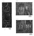
- FIG. 1A is an external view of the entire sliding portion
- FIG. 1B is an enlarged view of a portion A in FIG. 1A
- FIG. 1C is an enlarged view of a portion B in FIG.
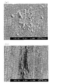
- 2A is an external view of the entire sliding portion
- FIG. 2B is an enlarged view of a portion A in FIG. 2A
- FIG. 2C is an enlarged view of a portion B in FIG.
- 3 (a) is an enlarged photograph of FIG. 1 (b), and FIG.
- FIG. 3 (b) is an enlarged photograph of FIG. 1 (c). It is the photograph which expanded and observed the sliding part of the comparative example after a sliding test.
- 4 (a) is an enlarged photograph of FIG. 2 (b), and FIG. 4 (b) is an enlarged photograph of FIG. 2 (c).
- FIG. 6A is a schematic side view showing the circular plate-like portion being separated from the sample
- FIG. 6B is a schematic side view showing the circular plate-like portion being in contact with the sample. It is a cross-sectional photograph which shows the working surface vicinity of the metal mold
- die of this invention is a metal mold
- die of this invention has is W (tungsten), Cr (chromium), Mo (molybdenum), V (vanadium), Zr (zirconium), Al (aluminum), Si (silicon), Nb (niobium) , Ta (tantalum) and Ti (titanium) are preferably selected from at least one carbide, nitride, carbonitride, oxide and boride.
- the metal phase of the mold of the present invention is preferably selected from at least one of Co (cobalt), Ni (nickel), Fe (iron), W (tungsten), and Mo (molybdenum). Note that the mold according to the present embodiment is composed of a WC—Co composite material in which tungsten carbide (WC) is selected as the hard phase and Co is selected as the metal phase unless otherwise specified.
- die of this invention has the reinforcement
- the reinforcing layer composed of this hard phase is a layer that is substantially free of a metal phase.
- the reinforcing layer can be produced by removing the metal phase from the surface of the mold composed of the hard phase and the metal phase. In the removal of the metal phase, there may be a portion that is not completely removed, so that the metal phase is substantially absent.
- the reinforcing layer is preferably a layer composed of a hard phase and voids, or a hard phase and a material other than the metal phase filling the voids. This void may be formed by removing the metal phase, or may be left as it is, or may be filled with a material other than the metal phase. Of course, some voids may remain.
- the ratio of the area of the hard phase relative to the total area of the hard phase and the area of the metal phase is the hard phase ratio in the area ratio by cross-sectional observation, it is stronger than the hard phase ratio of the main part of the mold of the present invention.
- the hard phase ratio of the layer is high, and the hard phase ratio of the reinforcing layer is preferably 99% or more.
- An example of a method for measuring this hard phase ratio is shown below. First, the mold is cut in a direction orthogonal to the work surface, and a predetermined magnification (10,000 times in this embodiment) is used using a scanning electron microscope (SEM) so that the work surface portion of the mold enters the field of view. Take a photo at (magnification).
- SEM scanning electron microscope
- a straight line B obtained by connecting the substantially planar hard phase upper surfaces forming the work surface with a straight line A and translating the straight line A in the depth direction of the mold at a position of at least 0.2 ⁇ m from the mold surface.
- substantially flat in the present specification means that there are cases where minute irregularities exist on the upper surface of the hard phase serving as a work surface or a curved surface having a very large radius of curvature is included, but the upper surface of the hard phase is included.
- the shape in which the planar shape is dominant to the extent that a straight line can be created is shown.
- a curve corresponding to the curvature may be used, and a curve having an interval of at least 0.2 ⁇ m from the surface curve in the depth direction may be used also in the depth direction.
- the work surface has an arithmetic average roughness Ra (conforming to JIS-B-0601-2001) of 0.1 ⁇ m or less and a skewness Rsk of ⁇ 0.01 or less. It is also important.
- the mold of the present invention has a convex curve on the work surface, since the convex curve of the surface of the work surface is wider with respect to the concave portion and the formation of sharp convex portions can be suppressed.
- the Rsk of the present invention is preferably ⁇ 1.0 or less.
- the present invention is particularly effective when the workpiece is made of a metal material.
- the reinforcing layer of the present invention is preferably formed at least from the surface of the work surface to a range of 0.2 ⁇ m in the depth direction. Thereby, the adhesion resistance mentioned above can be improved more.
- the reinforcing layer is more preferably formed in the depth direction from the surface of the work surface to a range of 0.5 ⁇ m, and more preferably in the range of 1 ⁇ m.
- a hard film hereinafter also simply referred to as a film
- the reinforcing layer is measured from the interface between the coating layer and the reinforcing layer.
- the diameter of the hard phase is preferably 1 ⁇ m or more in order to make it easier to form voids formed in the reinforcing layer.
- the upper limit of the diameter of the hard phase is not particularly limited, but may be about 15 ⁇ m in order to stably maintain the strength of the mold.
- the reinforcing layer is formed almost uniformly over the entire work surface by etching, so that the measurement device such as a scanning electron microscope (SEM) can be used in a cross section of the work surface. A range of about 10 ⁇ m to 20 ⁇ m in the inward direction may be confirmed.
- the diameter of the hard phase may be determined from the cross-sectional photograph using a section method (intercept method).
- the working surface of the mold of the present invention may be configured such that a diamond-like carbon film (hereinafter also referred to as a DLC film) is coated on the reinforcing layer as a hard film.
- a DLC film diamond-like carbon film
- the wear resistance of the mold is improved, and the DLC film also has unevenness on the surface of the film so as to follow the unevenness of the surface of the reinforcing layer, so that the advantages of providing the above-described voids can also be exhibited. I can expect.
- the DLC film has a hydrogen atom content of 0.5 atomic% or less on the surface of the DLC film and a nitrogen content of 2 atomic% or less. can do.
- the hydrogen content at the interface side with the reinforcing layer of the DLC film is 0.7 atomic% or more and 7 atomic% or less, and the nitrogen content is more than 2 atomic% and 10 atomic% or less, thereby further improving wear resistance. I can expect.
- the DLC film may contain metal (including metalloid) elements in order to impart characteristics such as wear resistance and heat resistance, and may be in the form of metal, alloy, or carbide, nitride, carbonitride. What is necessary is just to contain in the form of compounds, such as a thing, an oxide, and a carbon boride.
- the content ratio (atomic%) of metal (including metalloid) elements in the DLC film is 2% or more, and more preferably 5% or more.
- the content ratio (atomic%) of the metal (including metalloid) element in the DLC film can be set to 20% or less, more preferably 10% or less.
- the thickness of the DLC film can be set to 0.1 ⁇ m to 1.5 ⁇ m in order to further improve durability and adhesion to the mold, and may be set to 0.1 ⁇ m to 1.2 ⁇ m. In order to impart sufficient wear resistance to the mold, the film thickness of the DLC film may be set to 0.2 ⁇ m or more. In order to achieve smooth surface roughness and excellent wear resistance at the same time, the film thickness of the DLC film may be set to 0.5 ⁇ m to 1.2 ⁇ m.
- the mold of the present invention has at least one type of carbide, nitride, carbonitride, oxide and boron of the group 4, 5, 6 transition metal, Si, Al on the reinforcing layer. It is preferable to form one or more hard coatings selected from the chemicals. More preferably, a film made of Cr-based nitride, Ti-based nitride or Ti-based carbonitride is applied, and more preferably a film of TiCN, AlCrN, TiSiN, TiAlN, AlCrSiN, TiAlSiN, or TiAlCrSiN can be applied. Most preferably, a coating made of AlCrSiN is applied.
- the AlCrSiN in the composition formula of Al x Cr y Si z, controls a 20 ⁇ x ⁇ 75,25 ⁇ y ⁇ 75,0 ⁇ z ⁇ 10 It is preferable.
- TiAlSiN it is preferable to control 25 ⁇ x ⁇ 75, 20 ⁇ y ⁇ 75, and 0 ⁇ z ⁇ 10 in the composition formula of Ti x Al y Si z .
- the preferred film thickness of this film is 0.1 ⁇ m to 5.0 ⁇ m, the more preferred lower limit of the film thickness is 0.5 ⁇ m, and the upper limit is 2.0 ⁇ m.
- the film thickness is too thick, the convex portion of the hard phase cannot be traced, and the advantageous effects such as the above-mentioned adhesion resistance may not be exhibited. It may not be obtained sufficiently.
- the Al x Cr y Si z N film when used, it may have a gradient composition in which the y value decreases as the x value increases from the substrate side toward the coating surface side. Thereby, the adhesive strength with the substrate can be further improved. Since the hard phase is discretely formed on the surface of the film, and the hard film is continuously formed so as to cover the hard phase, the hard phase and the hard film can be observed by observing the cross section of the mold. Can be identified.
- the surface roughness of the film surface is preferably 0.1 ⁇ m or less in terms of arithmetic average roughness Ra and ⁇ 1.0 or less in terms of Rsk. More preferable Ra is 0.06 ⁇ m or less.
- Ra is 0.06 ⁇ m or less.
- a surface of a mold composed of a composite material including a hard phase and a metal phase is formed into a shape processing step of Ra ⁇ 0.1 ⁇ m, and after the shape processing step, Ra ⁇ 0.1 ⁇ m. And a surface layer modification step of etching the surface of the adjusted mold and removing the metal phase in the vicinity of the surface.
- a mold made of this composite material can be manufactured by an existing method. For example, after pressing and molding a mixed powder of a hard powder and a metal powder into a predetermined shape, 1250- It can be obtained by sintering at a temperature of 1550 ° C.
- the mixed powder used in the production method of the present invention preferably has a volume ratio of 97: 3 to 70:30 of the hard powder and the metal powder.
- the hard powder is W (tungsten), Cr (chromium), Mo (molybdenum), V (vanadium), Zr (zirconium), Al (aluminum), Si (silicon), Nb (niobium), Ta (tantalum).
- at least one kind of carbide, nitride, carbonitride, oxide, and boride of Ti (titanium), and the metal powder may be Co (cobalt), Ni (nickel), Fe ( It is preferably selected from at least one of iron, W (tungsten), and Mo (molybdenum).
- a shaping process is performed in which the surface of the prepared mold is adjusted to Ra ⁇ 0.1 ⁇ m by grinding, polishing, cutting, electric discharge machining or the like.
- the surface of the mold in particular, the surface of the mold serving as the work surface is smoothed, and a smooth and appropriate recess is formed through the subsequent surface layer reforming step.
- Ra ⁇ 0.1 ⁇ m, skewness Rsk ⁇ A working surface having a surface roughness of ⁇ 0.01 can be formed.
- a more preferable upper limit of Ra is 0.05 ⁇ m, and a more preferable upper limit of Ra is 0.02 ⁇ m.
- the lower limit is not particularly limited, but can be set to 0.001 ⁇ m, for example, in consideration of mass productivity.
- the shape processing step may be a combination of a plurality of steps. For example, after roughing by grinding, Ra ⁇ 0.1 ⁇ m may be adjusted by finishing by polishing. For the polishing at this time, an existing grinding method can be used, but buffing using a diamond paste may be performed in order to surely obtain a desired surface roughness.
- etching is applied to the surface layer modification step.
- wet etching using an acidic solution or alkaline solution or dry etching using discharge plasma can be used. More preferably, wet etching is used that facilitates the formation of a thick reinforcing layer composed of a hard phase and that can easily adjust Rsk to a negative value.
- an acidic solution such as hydrochloric acid, nitric acid, or aqua regia can be used as the etchant, but the removal capability of the metal phase is high and a reinforcing layer is formed. It is preferable to use aqua regia that is easy to cause.
- the etching process time is preferably more than 30 seconds in order to surely adjust Rsk to a value of ⁇ 1.0 ⁇ m or less. A more preferable processing time is 60 seconds or more, and a further preferable processing time is 90 seconds or more.
- dry etching is applied to the surface layer modification step, an existing method can be applied.
- the inside of a chamber for generating plasma is set to a reduced pressure Ar atmosphere of about 2 Pa, Ar gas is turned into plasma, and the substrate is etched with a bias of ⁇ 300 V so that a desired reinforcing layer is provided. Mold can be obtained.
- a DLC film as a hard film directly on the reinforcing layer in order to further improve the wear resistance.
- Existing coating methods such as sputtering and plasma CVD can be used to coat the DLC film, but if the filtered arc ion plating method is used, a smoother DLC film with fewer droplets is coated. I can expect that.
- a gas containing hydrogen such as nitrogen gas and / or hydrocarbon introduced into the furnace, It tends to be preferable to coat the DLC film.
- a hydrogen-containing mixed gas is used to remove the oxide film and dirt existing on the surface of the reinforcing layer while containing hydrogen on the surface of the DLC film on the reinforcing layer side. You may perform the used gas bombardment process.
- the hydrogen mixed gas at this time is more preferably a mixed gas containing argon gas and 4% by mass or more of hydrogen gas with respect to the total mass of the mixed gas.
- the 4, 5, 6 group transition metal, Si and Al carbides, nitrides You may coat
- the AlCrSiN in the composition formula of Al x Cr y Si z, 25 ⁇ x ⁇ 75,20 ⁇ y ⁇ 75,0.0 ⁇ controlling the z ⁇ 10 Is preferred.
- TiAlSiN it is preferable to control 25 ⁇ x ⁇ 75, 20 ⁇ y ⁇ 75, and 0.0 ⁇ z ⁇ 10 in the composition formula of Ti x Al y Si z .
- the PVD method can be used as a method for forming this film, but it is preferable to form the film using a sputtering method that can obtain a smoother film surface with less droplets.
- the bias voltage applied to the substrate it is more preferable to set the bias voltage applied to the substrate to 40 to 150 V in order to improve the adhesion strength between the substrate and the film while further improving the surface smoothness.
- a CVD method may be used, and a smoother film can be obtained by using the CVD method.
- TiCN is coated by a thermal CVD method, it is preferable to set the film thickness to 0.5 to 2.0 ⁇ m and the film forming temperature to 700 to 900 ° C.
- Reference numeral 2 denotes an example of the present invention in which a polished layer is subjected to plasma etching in an Ar atmosphere with a bias voltage of ⁇ 300 V and an atmospheric pressure of 2 Pa to remove Co (metal phase) to form a reinforcing layer.
- Sample No. which is a comparative example. No treatment was performed on No. 11 after polishing.
- FIG. 7 shows a photograph of the vicinity of the surface layer in the vertical cross section 1.
- reference numeral 20 is a hard phase
- reference numeral 21 is a metal phase
- reference numeral 22 is a gap
- reference numeral 23 is a Ni plating layer as a protective layer. From FIG.
- the metal phase 21 is removed to form voids 22, and it can be confirmed that a reinforcing layer composed of the hard phase 20 is formed.
- This reinforcing layer was a layer substantially free of a metal phase, and a thickness of at least 1 ⁇ m from the surface was formed as the reinforcing layer. Further, the hard phase ratio of the reinforcing layer was almost 100% within the range of 1 ⁇ m.
- the layer 23 is a Ni plating layer for protecting the mold surface when taking the cross-sectional observation photograph of FIG. If this Ni plating layer is formed, the shape can be maintained, for example, when the mold is cut.
- Sample No. 1 No. 2, No. 11 was measured for surface roughness.
- the measurement conditions were an evaluation length of 4 mm, a measurement speed of 0.3 mm / s, a cutoff value of 0.8 mm, and a filter type of Gaussian.
- the measurement results are shown in Table 1.
- No. which is an example of the present invention. 1 and No. Sample No. 2 has a surface No. 2 whose surface was smoothed by polishing.
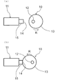
- FIGS. 5 and 6A and 6B A schematic diagram of the apparatus used in this sliding test is shown in FIGS. 5 and 6A and 6B.
- FIG. 5 is a top view of the test apparatus
- FIGS. 6A and 6B are side views of FIG.
- the test apparatus used in the present embodiment is in contact with and non-contacting the sample while rotating, with a holding mechanism 11 including an arm unit 15 for attaching and holding the sample to the sample setting unit 14.
- a contact jig 10 that repeats contact and a rotation mechanism (not shown) that rotatably holds the contact jig 10 are provided.
- the contact jig 10 includes a shaft portion 12 having a rotation axis Ax1 and a circular plate-like portion 13 having a central axis Ax2 that is eccentric from the rotation axis Ax1.
- the main body of the holding mechanism where the arm is installed has a storage hole for storing and holding the arm 15 so as to be able to move forward and backward.
- a resilient portion eg, a spring
- the test apparatus used in the present embodiment can perform wear evaluation of a mold material close to an actual use environment without preparing a mold that simulates an actual machining state.
- the samples of the present invention and the comparative example are attached to the tip of the arm portion 15 described above, and the SCM420-made circular plate-like portion (corresponding to the workpiece) is rotated at a rotational speed of 30 m / min to apply the normal drag applied to the sample.
- the samples of the present invention and the comparative example were slid 1000 times.
- the appearance of the sliding part of the sample of the present invention after the test is shown in FIG. 1, and the appearance of the sliding part of the sample of the comparative example is shown in FIG. From FIG. 1A and FIG.
- FIG. 3 (a) and FIG. 3 (a) and FIG. 3 (b) are enlarged photographs taken with the scanning electron microscope (SEM) of FIGS. 4 (a) and FIG. 3 (b) and FIG. 4 (b) show enlarged photographs by the scanning electron microscope (SEM) of FIG. 1 (c) and FIG. 4 (a) and 4 (b), which are comparative examples, confirm the adhered product from the workpiece. From FIGS. 3 (a) and 3 (b) which are examples of the present invention, the adhered product is shown.
- sample No. A sample prepared under the same conditions as in No. 1 was coated with a diamond-like carbon (DLC) film as a hard film. 3 was prepared.
- the film forming apparatus uses a filtered arc ion plating apparatus, and a negative pressure bias voltage applied to the substrate is set to ⁇ 2000 V, and a gas bombardment process using a mixed gas containing 5 mass% hydrogen gas in argon gas is performed. Performed for 90 minutes. The flow rate of the mixed gas was 50 sccm to 100 sccm.
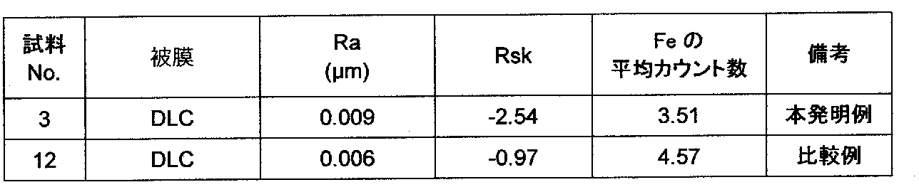
- Example 2 shows the evaluation results of Ra, Rsk, and the amount of adhesion.
- Specimen No. after test 3 is an enlarged photograph of the sliding part by SEM.
- the sliding part enlarged photograph by 12 SEM is shown in FIG. From FIG. 9 which is a comparative example, an adherent from the workpiece is confirmed, but from FIG. 8 which is an example of the present invention, the amount of the adherend from the workpiece is reduced. It was confirmed that the agglomerate suppression effect was exhibited. From Table 2, the sample of the comparative example had Ra ⁇ 0.1 ⁇ m and skewness Rsk ⁇ ⁇ 0.01 in Ra and Rsk, respectively. However, since the bonding layer on the substrate surface could not be removed, It was a result inferior to the example of this invention, since the adhesion suppression effect was not acquired. Sample No.
- FIG. 3 is a perspective photograph for observing the surface and cross section in the vicinity of the work surface of FIG. The perspective view of 12 is shown in FIG. As shown in FIG. No. 3 was able to confirm that the uneven shape of the substrate surface was transferred even when the DLC film was coated.
- Example 3 a film made of a material different from that in Example 2 was coated on the mold.
- No. The sample prepared under the same conditions as in No. 1 was coated with an AlCrSiN film. 4 was prepared.
- a sputtering apparatus was used as the film forming apparatus, a DC bias voltage of ⁇ 200 V was applied to the substrate, and cleaning with Ar ions was performed. Thereafter, N 2 gas was introduced into the container, a bias voltage was set to ⁇ 100 V, a sputtering power of 2 kW was supplied to the Ti target, and held for 10 minutes to cover the TiN bottom layer.
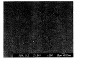
- Sample No. Fig. 12 shows an enlarged photograph of the sliding portion by SEM of No. 4. From Table 3, Sample No. 4 confirmed that Ra ⁇ 0.1 ⁇ m and skewness Rsk ⁇ ⁇ 0.01. In addition, the average count number of Fe was also the sample No. 11 or lower. It was confirmed that the sample No. 4 was able to exhibit high wear resistance while sufficiently exhibiting the adhesion suppressing effect.
Landscapes
- Chemical & Material Sciences (AREA)
- Engineering & Computer Science (AREA)
- Mechanical Engineering (AREA)
- Materials Engineering (AREA)
- Organic Chemistry (AREA)
- Metallurgy (AREA)
- Chemical Kinetics & Catalysis (AREA)
- General Chemical & Material Sciences (AREA)
- Manufacturing & Machinery (AREA)
- Mounting, Exchange, And Manufacturing Of Dies (AREA)
- Physical Vapour Deposition (AREA)
- Moulds For Moulding Plastics Or The Like (AREA)
- ing And Chemical Polishing (AREA)
- Molds, Cores, And Manufacturing Methods Thereof (AREA)
Abstract
Description
また引用文献2には、耐摩耗性に優れるダイヤモンド膜を密着性よく被覆するために、超硬合金の表面に元素周期律表IVa族、Va族、VIa族の金属炭化物、炭化ケイ素又はアルミナ等のセラミック粒子を埋め込んだ後、電解エッチング処理を施すことにより凹凸を形成し、その後この凹凸形成後にダイヤモンド膜を被覆する、被覆超硬合金が開示されている。
即ち本発明は、硬質相と金属相とを含む複合材料から構成される金型であって、
前記金型は、硬質相で構成される強化層を作業面に有し、
前記作業面は、算術平均粗さRa≦0.1μm、スキューネスRsk≦-0.01を満たしていることを特徴とする、金型である。
好ましくは、前記金型の表面は、スキューネスRsk≦-1.0である。
好ましくは、前記硬質相はWC,前記金属相はCoである。
また本発明は、硬質相と金属相とを含む複合材料から構成される金型であって、
前記金型は、硬質相で構成される強化層を作業面に有し、
前記強化層の上面に硬質皮膜を有し、
前記硬質皮膜は、4、5、6族遷移金属、Si、Alの少なくとも一種の炭化物、窒化物、炭窒化物、酸化物および硼化物、並びにダイヤモンドライクカーボンから選択される一種以上であり、
前記硬質皮膜の表面は、算術平均粗さRa≦0.1μm、スキューネスRsk≦-1.0であることを特徴とする、金型である。 また本発明の他の形態は、硬質相と金属相とを含む複合材料から構成される金型の製造方法であって、
前記複合材料から構成された金型の表面をRa≦0.1μmにする形状加工工程と、
前記形状加工工程の後、Ra≦0.1μmに調整された前記金型の表面をエッチングし、表面近傍の金属相をエッチングにより除去する、表層改質工程と、を有することを特徴とする、金型の製造方法である。
好ましくは、前記表層改質工程は、酸性溶液を使用したウェットエッチングである。
好ましくは、前記表層改質工程の後に、4、5、6族遷移金属、Si、Alの少なくとも一種の炭化物、窒化物、炭窒化物、酸化物および硼化物、並びにダイヤモンドライクカーボンの一種以上から選択される皮膜を金型表面に被覆する被覆工程を有する。
本発明の金型は、硬質相と、バインダ(結合相)としての金属相の二相が混在する複合材料から構成される金型である。この金型は、硬質相の利点(優れた強度)と金属相の利点(高い延性および靭性)とを併せ持つ特徴がある。
また本発明の金型が有する金属相は、Co(コバルト)、Ni(ニッケル)、Fe(鉄)、W(タングステン)、Mo(モリブデン)のうちの少なくとも一種から選択されることが好ましい。
なお本実施形態の金型は、特に記載がなければ、硬質相に炭化タングステン(WC)を、金属相にCoを選択したWC-Co複合材料から構成されている。
また、強化層は、硬質相と空隙、あるいは硬質相と空隙を埋める金属相以外の材料とから構成される層であることが好ましい。この空隙は、金属相が除去されて構成されるものであっても良く、空隙のままとしておいても良いし、この空隙に金属相以外の材料を充填したものでもよい。もちろん、一部の空隙が残存していてもよい。
この強化層が構成されていることにより、軟質で被加工材に凝着しやすい金属相が金型の作業面に存在しない構成とすることができるため、耐凝着性を格段に向上させて金型寿命の大幅な向上が期待できる。加えて本発明は、作業面の表面粗さが、算術平均粗さRa(JIS-B-0601-2001に準拠)が0.1μm以下であるとともに、スキューネスRskが-0.01以下であることも重要である。これにより本発明の金型は、作業面の表面の粗さ曲線は凹部に対して凸部の方が広くなり、先鋭な凸部の形成を抑制することができるため、作業面の凸部を起点とした摩耗やかじりの発生を大幅に抑制し、良好な摺動特性を発揮することが可能である。また金型および被加工材の作業面が平滑である場合、互いの作業面同士が接触している箇所に潤滑油を含浸させることは困難であるが、本発明ではRskを-0.01以下にすることで、金型の作業面に適度な凹部(以下、空隙とも記載する。)を形成させることで、潤滑油の含浸性を向上させ、良好な摺動特性を発揮させることが可能である。また、金型および被加工材の作業面が平滑である場合、真空凝着が生じる可能性があるが、上述した凹部により金型と被加工材との接触面が真空状態となることを防止することができ、その効果により良好な摺動特性を得ることが可能である。上述した効果をより確実に得るためにも、本発明のRskは-1.0以下であることが好ましい。尚、本発明は、被加工材が金属材料からなる場合に、特に効果を発揮する。
本発明の製造方法は、硬質相と金属相を含む複合材料から構成される金型の表面をRa≦0.1μmとする形状加工工程と、前記形状加工工程の後、Ra≦0.1μmに調整された金型の表面をエッチングし、表面近傍の金属相を除去する、表層改質工程と、を有することを特徴とする。この複合材料から構成される金型は既存の方法で作製することが可能であり、例えば、硬質粉末と金属粉末との混合粉末を所定の形状に加圧・成型後、真空雰囲気下で1250~1550℃の温度で焼結することで、得ることができる。なお金型の強度をより向上させるために、本発明の製造方法で用いる混合粉末は、硬質粉末と金属粉末とが体積比で、97:3~70:30であることが好ましい。また上記硬質粉末は、W(タングステン)、Cr(クロム)、Mo(モリブデン)、V(バナジウム)、Zr(ジルコニウム)、Al(アルミニウム)、Si(ケイ素)、Nb(ニオブ)、Ta(タンタル)およびTi(チタン)のうちの少なくとも一種の炭化物、窒化物、炭窒化物、酸化物および硼化物から選択されることが好ましく、上記金属粉末は、Co(コバルト)、Ni(ニッケル)、Fe(鉄)、W(タングステン)、Mo(モリブデン)のうちの少なくとも一種から選択されることが好ましい。
本発明の製造方法では用意した金型の表面を、研削加工、研磨加工、切削加工および放電加工等によりRa≦0.1μmに調整する形状加工工程を行う。この形状加工工程により金型の表面、特に作業面となる金型の表面を平滑にし、後の表層改質工程を経て、平滑かつ適度な凹部が形成され、Ra≦0.1μm、スキューネスRsk≦-0.01の表面粗さを有する作業面を形成させることができる。より好ましいRaの上限は0.05μm、さらに好ましいRaの上限は0.02μmである。下限は特に限定しないが、量産性を考慮して例えば0.001μmと設定することができる。ここで形状加工工程は複数の工程を組み合わせても良く、例えば研削加工で荒加工した後、研磨による仕上げ加工でRa≦0.1μmに調整しても良い。この時の研磨には、既存の研削方法を用いることができるが、所望の表面粗さを確実に得るために、ダイヤモンドペーストを用いたバフ研磨を実施してもよい。
続いて本発明の製造方法では、形状加工工程の後、Ra≦0.1μmに調整された金型の表面をエッチングし、表面近傍の金属相を除去する表層改質工程を行い、本発明の金型を得る。これにより金型の作業面に、硬質相で構成された強化層を形成させることができる。本発明ではこの表層改質工程にエッチングを適用しており、エッチングには酸性溶液やアルカリ性溶液を用いてエッチングするウェットエッチングや、放電プラズマを用いるドライエッチングを用いることができる。より好ましくは、硬質相で構成される強化層を厚く形成させやすく、Rskを安定して負値に調整しやすいウェットエッチングを用いる。
硬質相にWC、金属相にCoを選択した複合材料から構成される金型(超硬合金製)を準備した。この複合材料の硬質粉末と金属粉末との体積比は、82:18であった。この金型を、研削工具によりRa=1.5μmまで研削した後、ダイヤモンドペーストを用いたバフ研磨により金型の表面をRa=0.005μmとなるまで研磨した。試料No.1は、研磨後の金型表面を王水に60秒間浸漬させてCo(金属相)を除去して強化層を形成させた本発明例である。試料No.2は研磨後の金型表面にバイアス電圧-300V、雰囲気圧力2PaのAr雰囲気下でプラズマエッチングを施してCo(金属相)を除去し、強化層を形成させた本発明例である。比較例である試料No.11には、研磨後に何も処理を行わなかった。作製した試料No.1の垂直断面における表層付近の写真を図7に示す。図7において、符号20が硬質相、符号21が金属相、符号22が空隙、符号23が保護層のNiメッキ層である。図7より、試料No.1の表層(作業面25側)は金属相21が除去されて空隙22となっており、硬質相20から構成される強化層が形成されていることが確認できる。この強化層は実質的に金属相が存在しない層であり、表面から少なくとも1μmの厚さが強化層として形成されていた。また、その1μmの範囲内において、強化層の硬質相比率はほぼ100%であった。なお層23は、図7の断面観察写真の撮影に際して金型表面を保護するためのNiメッキ層である。このNiメッキ層を形成しておくと、例えば、金型を切断する時などに形状を保持させることができる。
試料No.1、No.2、No.11について表面粗さを測定した。表面粗さの測定には、東京精密(株)製触針式粗さ計(サーフコム)を用いた。測定条件は評価長さ4mm、測定速度0.3mm/s、カットオフ値0.8mm、フィルタ種別をガウシアンとした。測定結果を表1に示す。測定の結果、本発明例であるNo.1とNo.2の試料は、表面が研摩によって平滑に仕上げたのみのNo.11と比較してもRaの差が小さく、絶対値も0.1μm以下であり、十分な平滑性を有していることも確認できた。またNo.1、No.2の試料はRskが-0.01以下であり、No.11の試料よりも先鋭な凸部が少ないことが確認できた。特に王水によるウェットエッチングで処理を行ったNo.1の試料は、Rskが-1.6と大きい負値を示している。これは作業面の粗さ曲線における先鋭な凸部がさらに抑制されていることを示しており、このことから本発明の強化層が深くまで形成されていることが推定できる。表層改質処理を行っていない比較例である試料No.11は、Rsk>0であり、目標とする表面粗さを有していなかった。

続いてNo.1の条件で作製した本発明例の試料と、本発明の処理を施していない比較例の試料の摺動特性を比較する試験を行った。この摺動試験で用いた装置の模式図を図5、図6(a)(b)に示す。図5は試験装置の上面図であり、図6(a)(b)は図5の側面図である。上記の図に示すように、本実施形態で用いた試験装置は、試料設置部14に試料を取り付けて保持するアーム部15を含む保持機構11と、回転しながら上記試料に対して接触及び非接触を繰り返す接触治具10と、接触治具10を回転自在に保持する回転機構(図示省略)とを備えている。接触治具10は、回転軸Ax1を有する軸部12と、回転軸Ax1から偏心した中心軸Ax2を有する円形板状部13とから構成される。なお図5、6からは確認できないが、アーム部が設置される保持機構の本体部には、上記アーム部15を進退自在に収納保持する収納穴が形成されており、収納穴の中には弾発部(例:バネ)が設置されており、試料が垂直抗力を受けるとその試料を押し返すように構成されている。上述した構成により、本実施形態で用いる試験装置は、実際の加工状態を模擬した金型を準備しなくても、実際の使用環境に近い金型材料の摩耗評価を行うことができる。
上述したアーム部15の先端に本発明例および比較例の試料を取り付け、SCM420製の円形板状部(被加工材に相当する)を回転速度30m/minで回転させ、試料に付与する垂直抗力を120Nに設定し、本発明例および比較例の試料に1000回摺動させた。試験後の本発明例の試料の摺動部外観を図1に、比較例の試料の摺動部外観を図2に示す。図1(a)および図2(a)より、本発明例の試料は、比較例の試料よりも被加工材の凝着部が減少していることが確認できる。続いて被加工材の凝着が発生しやすい円形板状部の入口部である図1(b)および図2(b)の走査電子顕微鏡(SEM)による拡大写真を図3(a)および図4(a)に,出口部である図1(c)および図2(c)の走査電子顕微鏡(SEM)による拡大写真を図3(b)および図4(b)に示す。比較例である図4(a)、(b)からは被加工材からの凝着物が確認されるが、本発明例である図3(a)、(b)からは被加工材の凝着物が大幅に抑制されており、本発明例の試料の摺動性が大幅に向上していることが確認できた。また本発明例と比較例における凝着量を評価するために、電子線マイクロアナライザー(EPMA、日本電子製JXA‐8500F)による面分析を行い、マッピング結果の130μm×280μmの測定領域内におけるFeの平均カウント数を測定した。その結果、比較例の平均カウント数は38.17であったのに対し、本発明例の平均カウント数は12.84であり、本発明例の試料は比較例の試料よりも大幅にFeの凝着量を抑制することができたと考えられる。
次に被覆金型における本発明の効果を確認した。まず本発明例として、実施例1の試料No.1と同じ条件で作成した試料に、硬質皮膜としてダイヤモンドライクカーボン(DLC)膜を被覆した試料No.3を準備した。成膜装置には、フィルタードアークイオンプレーティング装置を用い、基材に印加する負圧のバイアス電圧を-2000Vとし、アルゴンガスに5質量%の水素ガスを含有した混合ガスによるガスボンバード処理を90分実施した。混合ガスの流量は50sccm~100sccmとした。ガスボンバード処理後、成膜チャンバーに10sccm窒素ガスを導入し、基材に-150Vのバイアス電圧を印加して、基材温度を100℃以下とした。そして、グラファイトターゲットに50Aの電流を投入し、DLC皮膜を約10分間被覆した。次いで、窒素ガスを5sccmとし、DLC皮膜を約10分間被覆した。次いで、窒素ガスの導入を止めて、DLC皮膜を30分間被覆し、試料No.3とした。なお比較例として、実施例1の比較例11にDLC皮膜を被覆したものを作成し、試料No.12とした。なおNo.3、No.12の皮膜厚みは、0.5μmであった。
続いて実施例2とは異なる材質の皮膜を金型に被覆した。本発明例として、実施例のNo.1と同じ条件で作成した試料に、AlCrSiN膜を被覆した試料No.4を準備した。成膜装置にはスパッタリング装置を用い、基材に-200Vの直流バイアス電圧を印加し、Arイオンによるクリーニングを実施した。その後容器内にN2ガスを導入し、バイアス電圧を-100Vに設定してTiターゲットに2kWのスパッタ電力を供給して、10分間保持し、TiN最下層を被覆した。続いて、バイアス電圧を-140Vに設定してAl65Cr35ターゲット(数値は原子比)に4kWのスパッタ電力を供給して、15分間保持し、AlCrN層を被覆した。続いて、Al65Cr35ターゲットに電力を供給した状態で、Al55Cr43Si2ターゲットに4kWのスパッタ電力を供給して、65分間保持し、AlCrSiN層を被覆した。この皮膜の総厚は、約2.7μmであった。結果を表3に示す。

11:ワーク保持機構
12:軸部
13:板状部
14:試料設置部
15:アーム部
20:硬質相
21:金属相
22:空隙
23:樹脂
25:作業面
26:硬質皮膜
Ax1:回転軸
Ax2:板状部の中心軸
Claims (7)
- 硬質相と金属相とを含む複合材料から構成される金型であって、
前記金型は、硬質相で構成される強化層を作業面に有し、
前記作業面は、算術平均粗さRa≦0.1μm、スキューネスRsk≦-0.01を満たしていることを特徴とする、金型。 - 前記金型の作業面は、スキューネスRsk≦-1.0であることを特徴とする、請求項1に記載の金型。
- 前記硬質相はWC、前記金属相はCoであることを特徴とする、請求項1または2に記載の金型。
- 硬質相と金属相とを含む複合材料から構成される金型であって、
前記金型は、硬質相で構成される強化層を作業面に有し、
前記強化層の上面に硬質皮膜を有し、
前記硬質皮膜は、4、5、6族遷移金属、Si、Alの少なくとも一種の炭化物、窒化物、炭窒化物、酸化物および硼化物、並びにダイヤモンドライクカーボンから選択される一種以上であり、
前記硬質皮膜の表面は、算術平均粗さRa≦0.1μm、スキューネスRsk≦-1.0であることを特徴とする、金型。 - 硬質相と金属相とを含む複合材料から構成される金型の製造方法であって、
前記複合材料から構成された金型の表面を加工してRa≦0.1μmに調整する形状加工工程と、
前記形状加工工程の後、Ra≦0.1μmに調整された前記金型の表面をエッチングし、表面近傍の金属相を除去する表層改質工程と、を有することを特徴とする、金型の製造方法。 - 前記表層改質工程は、酸性溶液を使用したウェットエッチングであることを特徴とする、請求項5に記載の金型の製造方法。
- 前記表層改質工程の後に、4、5、6族遷移金属、Si、Alの少なくとも一種の炭化物、窒化物、炭窒化物、酸化物および硼化物、並びにダイヤモンドライクカーボン選択される一種以上の硬質皮膜を金型表面に形成する被覆工程を有することを特徴とする、請求項5または6に記載の金型の製造方法。
Priority Applications (5)
| Application Number | Priority Date | Filing Date | Title |
|---|---|---|---|
| KR1020197015261A KR102252719B1 (ko) | 2016-11-28 | 2017-11-27 | 금형 및 그 제조 방법 |
| CN201780073512.2A CN110023052B (zh) | 2016-11-28 | 2017-11-27 | 金属材料加工用模具及其制造方法 |
| MYPI2019003017A MY191805A (en) | 2016-11-28 | 2017-11-27 | Mold and production method therefor |
| US16/464,301 US11820048B2 (en) | 2016-11-28 | 2017-11-27 | Mold and production method therefor |
| JP2018552998A JP7029646B2 (ja) | 2016-11-28 | 2017-11-27 | 金属材料加工用金型およびその製造方法、ならびに金型 |
Applications Claiming Priority (2)
| Application Number | Priority Date | Filing Date | Title |
|---|---|---|---|
| JP2016229852 | 2016-11-28 | ||
| JP2016-229852 | 2016-11-28 |
Publications (1)
| Publication Number | Publication Date |
|---|---|
| WO2018097286A1 true WO2018097286A1 (ja) | 2018-05-31 |
Family
ID=62195831
Family Applications (1)
| Application Number | Title | Priority Date | Filing Date |
|---|---|---|---|
| PCT/JP2017/042393 Ceased WO2018097286A1 (ja) | 2016-11-28 | 2017-11-27 | 金型およびその製造方法 |
Country Status (6)
| Country | Link |
|---|---|
| US (1) | US11820048B2 (ja) |
| JP (1) | JP7029646B2 (ja) |
| KR (1) | KR102252719B1 (ja) |
| CN (1) | CN110023052B (ja) |
| MY (1) | MY191805A (ja) |
| WO (1) | WO2018097286A1 (ja) |
Cited By (3)
| Publication number | Priority date | Publication date | Assignee | Title |
|---|---|---|---|---|
| CN112236243A (zh) * | 2018-07-04 | 2021-01-15 | 日本制铁株式会社 | 热压成型品的制造方法、压制成型品、冲模模具及模具套件 |
| JP7716608B1 (ja) * | 2025-04-11 | 2025-07-31 | 株式会社カムス | プレス成形金型の表面処理皮膜及びプレス成形金型 |
| JP7780839B1 (ja) * | 2024-12-24 | 2025-12-05 | 株式会社日進Prevo | ダイカスト金型用部品、ダイカスト金型およびそれを用いたダイカスト鋳造方法 |
Families Citing this family (2)
| Publication number | Priority date | Publication date | Assignee | Title |
|---|---|---|---|---|
| CN114274249B (zh) * | 2021-12-24 | 2024-02-02 | 厦门华天华电子有限公司 | 一种fpc模具冲头的加工方法 |
| KR102755160B1 (ko) * | 2023-10-10 | 2025-01-21 | 주식회사 이엠에스 | 고온 윤활 코팅이적용된 다이캐스팅 금형 및 부품 |
Citations (5)
| Publication number | Priority date | Publication date | Assignee | Title |
|---|---|---|---|---|
| JPH02188432A (ja) * | 1989-01-13 | 1990-07-24 | Hitachi Ltd | 光学部品の成形型 |
| JPH08216160A (ja) * | 1995-02-13 | 1996-08-27 | Hitachi Tool Eng Ltd | 樹脂成型用金型 |
| JP2008307687A (ja) * | 2007-06-12 | 2008-12-25 | Apic Yamada Corp | 樹脂成形用金型 |
| JP2010024518A (ja) * | 2008-07-23 | 2010-02-04 | Ibiden Engineering Kk | 金型の製造方法及び金型 |
| WO2016171273A1 (ja) * | 2015-04-23 | 2016-10-27 | 日立金属株式会社 | 被覆金型およびその製造方法 |
Family Cites Families (8)
| Publication number | Priority date | Publication date | Assignee | Title |
|---|---|---|---|---|
| US5380349A (en) * | 1988-12-07 | 1995-01-10 | Canon Kabushiki Kaisha | Mold having a diamond layer, for molding optical elements |
| US5246198A (en) * | 1990-06-01 | 1993-09-21 | Canon Kabushiki Kaisha | Diamond crystal coated mold for forming optical elements |
| JP3452615B2 (ja) | 1992-10-26 | 2003-09-29 | 三菱マテリアル神戸ツールズ株式会社 | 超硬合金、硬質炭素膜被覆超硬合金および超硬合金の製造方法並びにこれらの合金を応用した工具 |
| JPH0892741A (ja) | 1994-09-20 | 1996-04-09 | New Japan Radio Co Ltd | ダイヤモンド堆積用超硬合金の表面処理方法 |
| JP2005041107A (ja) * | 2003-07-22 | 2005-02-17 | Olympus Corp | プレス成形金型用複合材料の製造方法及びプレス成形金型用複合材料並びにプレス成形金型 |
| CN101102979A (zh) * | 2006-02-13 | 2008-01-09 | 松下电器产业株式会社 | 干蚀刻方法、微细结构形成方法、模板及模板的制造方法 |
| JP5217712B2 (ja) * | 2008-07-11 | 2013-06-19 | 株式会社豊田中央研究所 | 被覆超硬合金部材 |
| JP5351875B2 (ja) * | 2010-11-30 | 2013-11-27 | 株式会社神戸製鋼所 | 塑性加工用金型およびその製造方法、ならびにアルミニウム材の鍛造方法 |
-
2017
- 2017-11-27 CN CN201780073512.2A patent/CN110023052B/zh active Active
- 2017-11-27 MY MYPI2019003017A patent/MY191805A/en unknown
- 2017-11-27 KR KR1020197015261A patent/KR102252719B1/ko active Active
- 2017-11-27 US US16/464,301 patent/US11820048B2/en active Active
- 2017-11-27 WO PCT/JP2017/042393 patent/WO2018097286A1/ja not_active Ceased
- 2017-11-27 JP JP2018552998A patent/JP7029646B2/ja active Active
Patent Citations (5)
| Publication number | Priority date | Publication date | Assignee | Title |
|---|---|---|---|---|
| JPH02188432A (ja) * | 1989-01-13 | 1990-07-24 | Hitachi Ltd | 光学部品の成形型 |
| JPH08216160A (ja) * | 1995-02-13 | 1996-08-27 | Hitachi Tool Eng Ltd | 樹脂成型用金型 |
| JP2008307687A (ja) * | 2007-06-12 | 2008-12-25 | Apic Yamada Corp | 樹脂成形用金型 |
| JP2010024518A (ja) * | 2008-07-23 | 2010-02-04 | Ibiden Engineering Kk | 金型の製造方法及び金型 |
| WO2016171273A1 (ja) * | 2015-04-23 | 2016-10-27 | 日立金属株式会社 | 被覆金型およびその製造方法 |
Cited By (4)
| Publication number | Priority date | Publication date | Assignee | Title |
|---|---|---|---|---|
| CN112236243A (zh) * | 2018-07-04 | 2021-01-15 | 日本制铁株式会社 | 热压成型品的制造方法、压制成型品、冲模模具及模具套件 |
| JP7780839B1 (ja) * | 2024-12-24 | 2025-12-05 | 株式会社日進Prevo | ダイカスト金型用部品、ダイカスト金型およびそれを用いたダイカスト鋳造方法 |
| WO2026140630A1 (ja) * | 2024-12-24 | 2026-07-02 | 株式会社日進Prevo | ダイカスト金型用部品、ダイカスト金型およびそれを用いたダイカスト鋳造方法 |
| JP7716608B1 (ja) * | 2025-04-11 | 2025-07-31 | 株式会社カムス | プレス成形金型の表面処理皮膜及びプレス成形金型 |
Also Published As
| Publication number | Publication date |
|---|---|
| CN110023052B (zh) | 2022-05-31 |
| KR20190077459A (ko) | 2019-07-03 |
| KR102252719B1 (ko) | 2021-05-17 |
| JP7029646B2 (ja) | 2022-03-04 |
| JPWO2018097286A1 (ja) | 2019-10-17 |
| US11820048B2 (en) | 2023-11-21 |
| US20210107183A1 (en) | 2021-04-15 |
| MY191805A (en) | 2022-07-15 |
| CN110023052A (zh) | 2019-07-16 |
Similar Documents
| Publication | Publication Date | Title |
|---|---|---|
| CN101952482B (zh) | 多层涂覆的切削工具 | |
| JP7173026B2 (ja) | 切断工具およびその製造方法 | |
| JP7029646B2 (ja) | 金属材料加工用金型およびその製造方法、ならびに金型 | |
| CN107532279B (zh) | 包覆模具及其制造方法 | |
| US9371576B2 (en) | Coated tool and methods of making and using the coated tool | |
| JP5424103B2 (ja) | 塑性加工用被覆金型 | |
| JP5111379B2 (ja) | 切削工具及びその製造方法並びに切削方法 | |
| JP4842962B2 (ja) | 勾配形成元素としてバナジウムを用いた焼結超硬合金 | |
| WO2020194899A1 (ja) | 被覆切削工具 | |
| JP5839289B2 (ja) | 表面被覆切削工具 | |
| JP2013096004A (ja) | 耐剥離性に優れる被覆工具およびその製造方法 | |
| WO2020075356A1 (ja) | 切削工具及びその製造方法 | |
| CN102245801B (zh) | 制造对尺寸精度具有高要求的切削工具刀片的方法 | |
| JP6569376B2 (ja) | 超硬工具及びその製造方法 | |
| JP2008264988A (ja) | 切削工具の製造方法 | |
| JP6528936B2 (ja) | 被覆工具の製造方法 | |
| CN116372206A (zh) | 一种刀具用纳米涂层及涂层刀具 | |
| JP5240665B2 (ja) | すぐれた切屑排出性を示す表面被覆切削工具 | |
| JP5402155B2 (ja) | 表面被覆立方晶窒化ほう素基超高圧焼結材料製切削工具 | |
| JP6510771B2 (ja) | チタン又はチタン合金のミーリング加工用の被覆切削工具及びその製造方法 | |
| JP5229487B2 (ja) | すぐれた切屑排出性を示す表面被覆切削工具 | |
| JP2009090398A (ja) | 潤滑性および加工精度にすぐれたダイヤモンド被覆切削工具 | |
| JP7321412B2 (ja) | 表面被覆切削工具 | |
| JP2000308915A (ja) | 高送り切削で、切削面粗さの低下なく、すぐれた耐摩耗性を発揮する正面フライス工具 | |
| JP2010115704A (ja) | 塑性加工用被覆金型 |
Legal Events
| Date | Code | Title | Description |
|---|---|---|---|
| 121 | Ep: the epo has been informed by wipo that ep was designated in this application |
Ref document number: 17874566 Country of ref document: EP Kind code of ref document: A1 |
|
| ENP | Entry into the national phase |
Ref document number: 2018552998 Country of ref document: JP Kind code of ref document: A |
|
| ENP | Entry into the national phase |
Ref document number: 20197015261 Country of ref document: KR Kind code of ref document: A |
|
| NENP | Non-entry into the national phase |
Ref country code: DE |
|
| 122 | Ep: pct application non-entry in european phase |
Ref document number: 17874566 Country of ref document: EP Kind code of ref document: A1 |