WO2018097240A1 - レーザ装置及び光源装置 - Google Patents
レーザ装置及び光源装置 Download PDFInfo
- Publication number
- WO2018097240A1 WO2018097240A1 PCT/JP2017/042195 JP2017042195W WO2018097240A1 WO 2018097240 A1 WO2018097240 A1 WO 2018097240A1 JP 2017042195 W JP2017042195 W JP 2017042195W WO 2018097240 A1 WO2018097240 A1 WO 2018097240A1
- Authority
- WO
- WIPO (PCT)
- Prior art keywords
- laser
- side wall
- bottom plate
- plate portion
- present
- Prior art date
- Legal status (The legal status is an assumption and is not a legal conclusion. Google has not performed a legal analysis and makes no representation as to the accuracy of the status listed.)
- Ceased
Links
Images







Classifications
-
- H—ELECTRICITY
- H01—ELECTRIC ELEMENTS
- H01S—DEVICES USING THE PROCESS OF LIGHT AMPLIFICATION BY STIMULATED EMISSION OF RADIATION [LASER] TO AMPLIFY OR GENERATE LIGHT; DEVICES USING STIMULATED EMISSION OF ELECTROMAGNETIC RADIATION IN WAVE RANGES OTHER THAN OPTICAL
- H01S5/00—Semiconductor lasers
- H01S5/40—Arrangement of two or more semiconductor lasers, not provided for in groups H01S5/02 - H01S5/30
- H01S5/4018—Lasers electrically in series
-
- G—PHYSICS
- G02—OPTICS
- G02B—OPTICAL ELEMENTS, SYSTEMS OR APPARATUS
- G02B6/00—Light guides; Structural details of arrangements comprising light guides and other optical elements, e.g. couplings
- G02B6/24—Coupling light guides
- G02B6/42—Coupling light guides with opto-electronic elements
-
- G—PHYSICS
- G02—OPTICS
- G02B—OPTICAL ELEMENTS, SYSTEMS OR APPARATUS
- G02B6/00—Light guides; Structural details of arrangements comprising light guides and other optical elements, e.g. couplings
- G02B6/24—Coupling light guides
- G02B6/42—Coupling light guides with opto-electronic elements
- G02B6/4201—Packages, e.g. shape, construction, internal or external details
- G02B6/4204—Packages, e.g. shape, construction, internal or external details the coupling comprising intermediate optical elements, e.g. lenses, holograms
- G02B6/4206—Optical features
-
- G—PHYSICS
- G02—OPTICS
- G02B—OPTICAL ELEMENTS, SYSTEMS OR APPARATUS
- G02B6/00—Light guides; Structural details of arrangements comprising light guides and other optical elements, e.g. couplings
- G02B6/24—Coupling light guides
- G02B6/42—Coupling light guides with opto-electronic elements
- G02B6/4201—Packages, e.g. shape, construction, internal or external details
- G02B6/4204—Packages, e.g. shape, construction, internal or external details the coupling comprising intermediate optical elements, e.g. lenses, holograms
- G02B6/4214—Packages, e.g. shape, construction, internal or external details the coupling comprising intermediate optical elements, e.g. lenses, holograms the intermediate optical element having redirecting reflective means, e.g. mirrors, prisms for deflecting the radiation from horizontal to down- or upward direction toward a device
-
- G—PHYSICS
- G02—OPTICS
- G02B—OPTICAL ELEMENTS, SYSTEMS OR APPARATUS
- G02B6/00—Light guides; Structural details of arrangements comprising light guides and other optical elements, e.g. couplings
- G02B6/24—Coupling light guides
- G02B6/42—Coupling light guides with opto-electronic elements
- G02B6/4201—Packages, e.g. shape, construction, internal or external details
- G02B6/4256—Details of housings
- G02B6/4257—Details of housings having a supporting carrier or a mounting substrate or a mounting plate
-
- H—ELECTRICITY
- H01—ELECTRIC ELEMENTS
- H01S—DEVICES USING THE PROCESS OF LIGHT AMPLIFICATION BY STIMULATED EMISSION OF RADIATION [LASER] TO AMPLIFY OR GENERATE LIGHT; DEVICES USING STIMULATED EMISSION OF ELECTROMAGNETIC RADIATION IN WAVE RANGES OTHER THAN OPTICAL
- H01S3/00—Lasers, i.e. devices using stimulated emission of electromagnetic radiation in the infrared, visible or ultraviolet wave range
- H01S3/05—Construction or shape of optical resonators; Accommodation of active medium therein; Shape of active medium
- H01S3/06—Construction or shape of active medium
- H01S3/063—Waveguide lasers, i.e. whereby the dimensions of the waveguide are of the order of the light wavelength
- H01S3/067—Fibre lasers
-
- H—ELECTRICITY
- H01—ELECTRIC ELEMENTS
- H01S—DEVICES USING THE PROCESS OF LIGHT AMPLIFICATION BY STIMULATED EMISSION OF RADIATION [LASER] TO AMPLIFY OR GENERATE LIGHT; DEVICES USING STIMULATED EMISSION OF ELECTROMAGNETIC RADIATION IN WAVE RANGES OTHER THAN OPTICAL
- H01S3/00—Lasers, i.e. devices using stimulated emission of electromagnetic radiation in the infrared, visible or ultraviolet wave range
- H01S3/09—Processes or apparatus for excitation, e.g. pumping
- H01S3/091—Processes or apparatus for excitation, e.g. pumping using optical pumping
- H01S3/094—Processes or apparatus for excitation, e.g. pumping using optical pumping by coherent light
- H01S3/0941—Processes or apparatus for excitation, e.g. pumping using optical pumping by coherent light of a laser diode
-
- H—ELECTRICITY
- H01—ELECTRIC ELEMENTS
- H01S—DEVICES USING THE PROCESS OF LIGHT AMPLIFICATION BY STIMULATED EMISSION OF RADIATION [LASER] TO AMPLIFY OR GENERATE LIGHT; DEVICES USING STIMULATED EMISSION OF ELECTROMAGNETIC RADIATION IN WAVE RANGES OTHER THAN OPTICAL
- H01S5/00—Semiconductor lasers
- H01S5/02—Structural details or components not essential to laser action
- H01S5/022—Mountings; Housings
- H01S5/02208—Mountings; Housings characterised by the shape of the housings
- H01S5/02216—Butterfly-type, i.e. with electrode pins extending horizontally from the housings
-
- H—ELECTRICITY
- H01—ELECTRIC ELEMENTS
- H01S—DEVICES USING THE PROCESS OF LIGHT AMPLIFICATION BY STIMULATED EMISSION OF RADIATION [LASER] TO AMPLIFY OR GENERATE LIGHT; DEVICES USING STIMULATED EMISSION OF ELECTROMAGNETIC RADIATION IN WAVE RANGES OTHER THAN OPTICAL
- H01S5/00—Semiconductor lasers
- H01S5/02—Structural details or components not essential to laser action
- H01S5/022—Mountings; Housings
- H01S5/0225—Out-coupling of light
- H01S5/02251—Out-coupling of light using optical fibres
-
- H—ELECTRICITY
- H01—ELECTRIC ELEMENTS
- H01S—DEVICES USING THE PROCESS OF LIGHT AMPLIFICATION BY STIMULATED EMISSION OF RADIATION [LASER] TO AMPLIFY OR GENERATE LIGHT; DEVICES USING STIMULATED EMISSION OF ELECTROMAGNETIC RADIATION IN WAVE RANGES OTHER THAN OPTICAL
- H01S5/00—Semiconductor lasers
- H01S5/02—Structural details or components not essential to laser action
- H01S5/022—Mountings; Housings
- H01S5/023—Mount members, e.g. sub-mount members
- H01S5/02325—Mechanically integrated components on mount members or optical micro-benches
- H01S5/02326—Arrangements for relative positioning of laser diodes and optical components, e.g. grooves in the mount to fix optical fibres or lenses
-
- H—ELECTRICITY
- H01—ELECTRIC ELEMENTS
- H01S—DEVICES USING THE PROCESS OF LIGHT AMPLIFICATION BY STIMULATED EMISSION OF RADIATION [LASER] TO AMPLIFY OR GENERATE LIGHT; DEVICES USING STIMULATED EMISSION OF ELECTROMAGNETIC RADIATION IN WAVE RANGES OTHER THAN OPTICAL
- H01S5/00—Semiconductor lasers
- H01S5/02—Structural details or components not essential to laser action
- H01S5/022—Mountings; Housings
- H01S5/0233—Mounting configuration of laser chips
- H01S5/02345—Wire-bonding
-
- H—ELECTRICITY
- H01—ELECTRIC ELEMENTS
- H01S—DEVICES USING THE PROCESS OF LIGHT AMPLIFICATION BY STIMULATED EMISSION OF RADIATION [LASER] TO AMPLIFY OR GENERATE LIGHT; DEVICES USING STIMULATED EMISSION OF ELECTROMAGNETIC RADIATION IN WAVE RANGES OTHER THAN OPTICAL
- H01S5/00—Semiconductor lasers
- H01S5/02—Structural details or components not essential to laser action
- H01S5/022—Mountings; Housings
- H01S5/0239—Combinations of electrical or optical elements
-
- G—PHYSICS
- G02—OPTICS
- G02B—OPTICAL ELEMENTS, SYSTEMS OR APPARATUS
- G02B6/00—Light guides; Structural details of arrangements comprising light guides and other optical elements, e.g. couplings
- G02B6/24—Coupling light guides
- G02B6/42—Coupling light guides with opto-electronic elements
- G02B6/4201—Packages, e.g. shape, construction, internal or external details
- G02B6/4266—Thermal aspects, temperature control or temperature monitoring
- G02B6/4268—Cooling
- G02B6/4272—Cooling with mounting substrates of high thermal conductivity
-
- H—ELECTRICITY
- H01—ELECTRIC ELEMENTS
- H01S—DEVICES USING THE PROCESS OF LIGHT AMPLIFICATION BY STIMULATED EMISSION OF RADIATION [LASER] TO AMPLIFY OR GENERATE LIGHT; DEVICES USING STIMULATED EMISSION OF ELECTROMAGNETIC RADIATION IN WAVE RANGES OTHER THAN OPTICAL
- H01S3/00—Lasers, i.e. devices using stimulated emission of electromagnetic radiation in the infrared, visible or ultraviolet wave range
- H01S3/05—Construction or shape of optical resonators; Accommodation of active medium therein; Shape of active medium
- H01S3/06—Construction or shape of active medium
- H01S3/063—Waveguide lasers, i.e. whereby the dimensions of the waveguide are of the order of the light wavelength
- H01S3/067—Fibre lasers
- H01S3/0675—Resonators including a grating structure, e.g. distributed Bragg reflectors [DBR] or distributed feedback [DFB] fibre lasers
-
- H—ELECTRICITY
- H01—ELECTRIC ELEMENTS
- H01S—DEVICES USING THE PROCESS OF LIGHT AMPLIFICATION BY STIMULATED EMISSION OF RADIATION [LASER] TO AMPLIFY OR GENERATE LIGHT; DEVICES USING STIMULATED EMISSION OF ELECTROMAGNETIC RADIATION IN WAVE RANGES OTHER THAN OPTICAL
- H01S3/00—Lasers, i.e. devices using stimulated emission of electromagnetic radiation in the infrared, visible or ultraviolet wave range
- H01S3/09—Processes or apparatus for excitation, e.g. pumping
- H01S3/091—Processes or apparatus for excitation, e.g. pumping using optical pumping
- H01S3/094—Processes or apparatus for excitation, e.g. pumping using optical pumping by coherent light
- H01S3/094003—Processes or apparatus for excitation, e.g. pumping using optical pumping by coherent light the pumped medium being a fibre
-
- H—ELECTRICITY
- H01—ELECTRIC ELEMENTS
- H01S—DEVICES USING THE PROCESS OF LIGHT AMPLIFICATION BY STIMULATED EMISSION OF RADIATION [LASER] TO AMPLIFY OR GENERATE LIGHT; DEVICES USING STIMULATED EMISSION OF ELECTROMAGNETIC RADIATION IN WAVE RANGES OTHER THAN OPTICAL
- H01S3/00—Lasers, i.e. devices using stimulated emission of electromagnetic radiation in the infrared, visible or ultraviolet wave range
- H01S3/09—Processes or apparatus for excitation, e.g. pumping
- H01S3/091—Processes or apparatus for excitation, e.g. pumping using optical pumping
- H01S3/094—Processes or apparatus for excitation, e.g. pumping using optical pumping by coherent light
- H01S3/094049—Guiding of the pump light
- H01S3/094053—Fibre coupled pump, e.g. delivering pump light using a fibre or a fibre bundle
-
- H—ELECTRICITY
- H01—ELECTRIC ELEMENTS
- H01S—DEVICES USING THE PROCESS OF LIGHT AMPLIFICATION BY STIMULATED EMISSION OF RADIATION [LASER] TO AMPLIFY OR GENERATE LIGHT; DEVICES USING STIMULATED EMISSION OF ELECTROMAGNETIC RADIATION IN WAVE RANGES OTHER THAN OPTICAL
- H01S3/00—Lasers, i.e. devices using stimulated emission of electromagnetic radiation in the infrared, visible or ultraviolet wave range
- H01S3/09—Processes or apparatus for excitation, e.g. pumping
- H01S3/091—Processes or apparatus for excitation, e.g. pumping using optical pumping
- H01S3/094—Processes or apparatus for excitation, e.g. pumping using optical pumping by coherent light
- H01S3/09408—Pump redundancy
-
- H—ELECTRICITY
- H01—ELECTRIC ELEMENTS
- H01S—DEVICES USING THE PROCESS OF LIGHT AMPLIFICATION BY STIMULATED EMISSION OF RADIATION [LASER] TO AMPLIFY OR GENERATE LIGHT; DEVICES USING STIMULATED EMISSION OF ELECTROMAGNETIC RADIATION IN WAVE RANGES OTHER THAN OPTICAL
- H01S3/00—Lasers, i.e. devices using stimulated emission of electromagnetic radiation in the infrared, visible or ultraviolet wave range
- H01S3/09—Processes or apparatus for excitation, e.g. pumping
- H01S3/091—Processes or apparatus for excitation, e.g. pumping using optical pumping
- H01S3/094—Processes or apparatus for excitation, e.g. pumping using optical pumping by coherent light
- H01S3/0941—Processes or apparatus for excitation, e.g. pumping using optical pumping by coherent light of a laser diode
- H01S3/09415—Processes or apparatus for excitation, e.g. pumping using optical pumping by coherent light of a laser diode the pumping beam being parallel to the lasing mode of the pumped medium, e.g. end-pumping
-
- H—ELECTRICITY
- H01—ELECTRIC ELEMENTS
- H01S—DEVICES USING THE PROCESS OF LIGHT AMPLIFICATION BY STIMULATED EMISSION OF RADIATION [LASER] TO AMPLIFY OR GENERATE LIGHT; DEVICES USING STIMULATED EMISSION OF ELECTROMAGNETIC RADIATION IN WAVE RANGES OTHER THAN OPTICAL
- H01S5/00—Semiconductor lasers
- H01S5/005—Optical components external to the laser cavity, specially adapted therefor, e.g. for homogenisation or merging of the beams or for manipulating laser pulses, e.g. pulse shaping
-
- H—ELECTRICITY
- H01—ELECTRIC ELEMENTS
- H01S—DEVICES USING THE PROCESS OF LIGHT AMPLIFICATION BY STIMULATED EMISSION OF RADIATION [LASER] TO AMPLIFY OR GENERATE LIGHT; DEVICES USING STIMULATED EMISSION OF ELECTROMAGNETIC RADIATION IN WAVE RANGES OTHER THAN OPTICAL
- H01S5/00—Semiconductor lasers
- H01S5/005—Optical components external to the laser cavity, specially adapted therefor, e.g. for homogenisation or merging of the beams or for manipulating laser pulses, e.g. pulse shaping
- H01S5/0071—Optical components external to the laser cavity, specially adapted therefor, e.g. for homogenisation or merging of the beams or for manipulating laser pulses, e.g. pulse shaping for beam steering, e.g. using a mirror outside the cavity to change the beam direction
-
- H—ELECTRICITY
- H01—ELECTRIC ELEMENTS
- H01S—DEVICES USING THE PROCESS OF LIGHT AMPLIFICATION BY STIMULATED EMISSION OF RADIATION [LASER] TO AMPLIFY OR GENERATE LIGHT; DEVICES USING STIMULATED EMISSION OF ELECTROMAGNETIC RADIATION IN WAVE RANGES OTHER THAN OPTICAL
- H01S5/00—Semiconductor lasers
- H01S5/40—Arrangement of two or more semiconductor lasers, not provided for in groups H01S5/02 - H01S5/30
- H01S5/4012—Beam combining, e.g. by the use of fibres, gratings, polarisers, prisms
-
- H—ELECTRICITY
- H01—ELECTRIC ELEMENTS
- H01S—DEVICES USING THE PROCESS OF LIGHT AMPLIFICATION BY STIMULATED EMISSION OF RADIATION [LASER] TO AMPLIFY OR GENERATE LIGHT; DEVICES USING STIMULATED EMISSION OF ELECTROMAGNETIC RADIATION IN WAVE RANGES OTHER THAN OPTICAL
- H01S5/00—Semiconductor lasers
- H01S5/40—Arrangement of two or more semiconductor lasers, not provided for in groups H01S5/02 - H01S5/30
- H01S5/4025—Array arrangements, e.g. constituted by discrete laser diodes or laser bar
- H01S5/4031—Edge-emitting structures
- H01S5/4043—Edge-emitting structures with vertically stacked active layers
- H01S5/405—Two-dimensional arrays
Definitions
- the present invention relates to a laser device having a semiconductor laser element and a light source device having a plurality of laser devices.
- Semiconductor lasers have features such as low power consumption and small size, and have been widely used in various fields such as optical communication, optical recording, and material processing.
- a semiconductor laser module on which a semiconductor laser is mounted a module in which a plurality of semiconductor lasers are provided in a package is known (Patent Document 1).
- an optical element such as a semiconductor laser element or a lens is accommodated in a package casing.
- a side wall portion of the package housing is provided with a terminal portion including an electrode such as a lead pin and an output portion including an optical fiber.
- the electrode of the terminal part provided in the side wall part of the housing needs to be electrically connected to the semiconductor laser element housed in the housing.
- casing needs to align with respect to the laser beam which was output from the semiconductor laser element accommodated in a housing
- the semiconductor laser element or the like housed in the housing is electrically connected to or optically aligned with the member provided on the side wall portion of the housing. It is necessary to do. For this reason, the conventional semiconductor laser module is not good in assemblability, and therefore it is difficult to manufacture at low cost.
- An object of the present invention has been made in view of the above, and it is an object of the present invention to provide a laser device that has good assemblability and can be manufactured at low cost, and a light source device using the same.
- a bottom plate portion a semiconductor laser element installed on the bottom plate portion, a lid portion provided on the bottom plate portion on which the semiconductor laser element is installed, and having a top plate portion; And a side wall covering a part or all of the side of the space between the bottom plate and the top plate, and the top plate is formed integrally with a part or all of the side wall.
- a laser device is provided.
- a light source device including the plurality of laser devices described above and a base member having an installation surface on which the plurality of laser devices are installed.
- the light source device described above an amplification optical fiber, and an incident unit that causes laser light output from the plurality of laser devices of the light source device to enter the amplification optical fiber;
- An optical fiber laser is provided.
- the present invention it is possible to provide a laser device that has good assemblability and can be manufactured at low cost, and a light source device using the laser device.
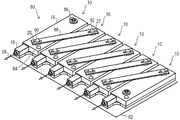
- FIG. 1A is a schematic view showing a laser apparatus according to a first embodiment of the present invention.
- FIG. 1B is a schematic view showing a laser apparatus according to the first embodiment of the present invention.
- FIG. 2A is a schematic diagram illustrating a light source device according to a first embodiment of the present invention.
- FIG. 2B is a schematic diagram illustrating the light source device according to the first embodiment of the present invention.
- FIG. 3 is a schematic view showing an optical fiber laser using the light source device according to the first embodiment of the present invention as an excitation light source.
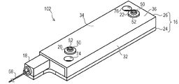
- FIG. 4A is a schematic view showing a laser apparatus according to the second embodiment of the present embodiment.
- FIG. 4B is a schematic view showing a laser apparatus according to the second embodiment of the present embodiment.
- FIG. 4A is a schematic view showing a laser apparatus according to the second embodiment of the present embodiment.
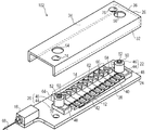
- FIG. 5A is a schematic view showing a laser apparatus according to the third embodiment of the present embodiment.
- FIG. 5B is a schematic view showing a laser apparatus according to the third embodiment of the present embodiment.
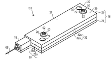
- FIG. 6A is a schematic view showing a laser apparatus according to the fourth embodiment of the present embodiment.
- FIG. 6B is a schematic view showing a laser apparatus according to the fourth embodiment of the present embodiment.
- FIG. 7 is a perspective view showing a laser apparatus according to a fifth embodiment of the present invention.
- FIG. 8 is a plan view showing a light source device according to a fifth embodiment of the present invention.
- FIG. 9 is a perspective view showing a laser apparatus according to the sixth embodiment of the present invention.
- FIG. 10 is a perspective view showing a laser apparatus according to the seventh embodiment of the present invention.
- FIG. 10 is a perspective view showing a laser apparatus according to the seventh embodiment of the present invention.
- FIG. 11 is a plan view showing a light source device according to an eighth embodiment of the present invention.
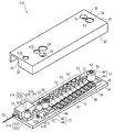
- FIG. 12 is an exploded perspective view showing a laser apparatus according to the ninth embodiment of the present invention.
- FIG. 13 is an enlarged perspective view showing electronic components and terminal portions in the laser apparatus according to the ninth embodiment of the present invention.
- FIG. 1A is a perspective view showing the laser apparatus according to the present embodiment.
- FIG. 1B is an exploded perspective view showing the laser apparatus according to the present embodiment.
- the laser apparatus according to the present embodiment is a semiconductor laser module having a plurality of semiconductor laser elements as laser elements.
- the laser apparatus 10 according to the present embodiment includes a plurality of semiconductor laser elements 12 and an optical system 14 provided corresponding to the plurality of semiconductor laser elements 12.
- the laser device 10 according to the present embodiment includes a package housing 16 that houses a plurality of semiconductor laser elements 12, an optical system 14, and the like.
- the laser apparatus 10 according to the present embodiment includes an output unit 18 that outputs laser light, and terminal units 20 and 22 that can be electrically connected to the outside.
- the housing 16 has, for example, a flat, substantially rectangular parallelepiped shape, and includes a bottom plate portion 24 and a lid portion 26.
- the lid portion 26 includes a front side wall portion 28 and a rear side wall portion 30 that face each other in the longitudinal direction of the housing 16, and a left side wall portion 32 and a right side wall portion 34 that face each other in the short side direction of the housing 16. ing. Further, the lid portion 26 has a top plate portion 36 provided on each side wall portion 28, 30, 32, 34 so as to face the bottom plate portion 24.
- the lid portion 26 is fixed on the bottom plate portion 24 so as to cover the plurality of semiconductor laser elements 12, the optical system 14, and the like provided on the bottom surface of the bottom plate portion 24 with an internal space.
- the lid 26 has a dustproof function for preventing dust from entering the housing 16 and a light blocking function for blocking light leakage to the outside of the housing 16 and light from entering the housing 16. .
- casing 16 is not specifically limited, A various shape is employable.
- the top plate part 36 is formed integrally with the side wall parts of the front side wall part 28, the rear side wall part 30, the left side wall part 32 and the right side wall part 34. That is, between the top plate portion 36 and the side wall portions of the front side wall portion 28, the rear side wall portion 30, the left side wall portion 32, and the right side wall portion 34, for example, a joint portion or a joint by welding, bonding, screwing, or the like. There is no, and the top plate part 36 and each side wall part are united. Note that there are no joints or joints between the front side wall portion 28 and the left and right side wall portions 32 and 34 by welding, bonding, screwing, or the like.
- the lid portion 26 is formed by integrally forming the top plate portion 36 and the front side wall portion 28, the rear side wall portion 30, the left side wall portion 32, and the right side wall portion 34.
- the front side wall 28, the rear side wall 30, the left side wall 32 and the right side wall 34 formed integrally with the top plate 36 are respectively a front side and a rear side of the space between the bottom plate 24 and the top plate 36. Covers the sides, left and right sides. In this way, the side walls formed integrally with the top plate portion 36 cover all the sides of the space between the bottom plate portion 24 and the top plate portion 36.
- the lid portion 26 in which the top plate portion 36 and the side wall portions are integrally formed as described above can be formed by, for example, injection molding, cutting, casting, plastic working, or the like. More specifically, as the injection molding, for example, metal injection molding (MIM) or resin injection molding can be used. Further, as a casting method, for example, a die casting method can be used. Further, as the plastic working, for example, press working such as bending or drawing can be used. In addition, the method of forming the cover part 26 is not limited to these. The lid portion 26 can be formed using various other methods.
- the front side wall portion 28, the rear side wall portion 30, the left side wall portion 32, and the right side wall portion 34 are provided so as to cover all the sides of the space between the bottom plate portion 24 and the top plate portion 36. It is not necessary to be formed integrally with the top plate portion 36.
- the side wall portion formed integrally with the top plate portion 36 only needs to cover at least a part of the side of the space between the bottom plate portion 24 and the top plate portion 36.
- the top plate portion 36 includes a front side wall portion 28, a rear side wall portion 30, a left side wall portion 32, and a right side wall portion, which are side wall portions that cover all the sides of the space between the bottom plate portion 24 and the top plate portion 36. It is not necessary to be formed integrally with all of 34.
- the top plate portion 36 only needs to be formed integrally with part or all of the side wall portion that covers a part or all of the side of the space between the bottom plate portion 24 and the top plate portion 36.
- a part of the front side wall 28, the rear side wall 30, the left side wall 32, and the right side wall 34 may be provided on the bottom plate 24 instead of the top plate 36. Further, a part of the front side wall 28, the rear side wall 30, the left side wall 32 and the right side wall 34 is not provided, and the side of the space between the top plate 36 and the bottom plate 24 is not provided. Some may be opened. These cases will be described in detail in the second to fourth embodiments.
- the material constituting the bottom plate portion 24 and the lid portion 26 constituting the housing 16 may be the same type of material or different materials, for example, metal or resin.
- the bottom plate portion 24 can be made of metal while the lid portion 26 can be made of resin.
- the material constituting the bottom plate portion 24 is the material constituting the lid portion 26, that is, the top plate portion 36, the front side wall portion 28, the rear side wall portion 30, the left side wall portion 32, and the right side wall portion formed integrally with each other.
- the thermal conductivity is higher than that of the material constituting the material 34. That is, it is preferable that the heat conduction of the bottom plate portion 24 is higher than the heat conductivity of the lid portion 26.
- the heat conductivity of the bottom plate part 24 in which the semiconductor laser element 12 that generates heat is provided as described later is relatively high, while the heat conductivity of the lid part 26 is lower than the heat conductivity of the bottom plate part 24.
- excellent heat dissipation characteristics can be obtained while suppressing an increase in product cost.
- the lid portion 26 is fixed on the bottom plate portion 24 by, for example, an adhesive, screwing, soldering, or the like.
- the housing 16 in which the lid portion 26 is fixed on the bottom plate portion 24 is not hermetically sealed and is not hermetically sealed.
- a plurality of semiconductor laser elements 12, an optical system 14, and a condenser lens 64 described later are accommodated in the housing 16. Further, the housing 16 accommodates portions other than the portions of the terminal portions 20 and 22 that protrude outside the housing 16 as will be described later.
- the bottom plate portion 24 is a portion that is installed with its lower surface in contact with the installation surface of the substrate when the laser device 10 is installed on the substrate.
- a step portion 38 is provided on the bottom plate portion 24 .
- the stepped portion 38 is stepped and has a plurality of steps 40 provided so as to be arranged along the front-rear direction of the housing 16.
- the plurality of steps 40 of the stepped portion 38 are gradually increased from the front to the rear.
- the step portion 38 may be formed integrally with the bottom plate portion 24 or may be a separate part fixed to the bottom plate portion 24 by soldering or the like. Note that, as described above, the thermal conductivity of the bottom plate portion 24 can be made higher than the thermal conductivity of the lid portion 26. Thereby, the outstanding heat dissipation characteristic can be acquired, suppressing the raise of product cost.
- a plurality of semiconductor laser elements 12 are installed on the bottom plate portion 24 and the plurality of steps 40 of the stepped portion 38.
- the plurality of semiconductor laser elements 12 are, for example, the same semiconductor laser element having the same oscillation wavelength, output, and other laser characteristics.
- the number of the plurality of semiconductor laser elements 12 is not particularly limited, and can be set as appropriate according to the laser output required for the laser device 10.
- the plurality of semiconductor laser elements 12 are mutually independent elements formed on separate chips.
- Each semiconductor laser element 12 is, for example, in the form of a chip on submount (COS) that is fixedly mounted on the submount 42 by soldering or the like, and has a plurality of steps on the bottom plate portion 24 and the stepped portion 38. 40 is installed.
- COS chip on submount
- the plurality of semiconductor laser elements 12 installed on the bottom plate portion 24 and the plurality of steps 40 of the step portion 38 are arranged in a line along the longitudinal direction of the housing 16.
- a height difference due to the stepped portion 38 is provided between the plurality of semiconductor laser elements 12 arranged in a line.
- the plurality of semiconductor laser elements 12 are arranged such that the output direction of the laser light is the short direction of the housing 16.
- the plurality of semiconductor laser elements 12 arranged in a line are arranged so as to output laser light on the same one side with respect to the arrangement. Note that the arrangement of the plurality of semiconductor laser elements 12 is not limited to one row, and a plurality of rows may be provided.
- the electrodes of the adjacent semiconductor laser elements 12 are electrically connected by wire bonding or the like. Thereby, the plurality of semiconductor laser elements 12 are connected in series.
- the method of electrically connecting the semiconductor laser elements 12 is not particularly limited, and various methods can be used. For example, a method by wire bonding described in Japanese Patent Application Laid-Open No. 2015-185667 is used. Can be used.
- a terminal portion 20 is provided on the bottom plate portion 24 in the casing 16 on the front side of the array of the plurality of semiconductor laser elements 12.
- a terminal portion 22 is provided on the bottom plate portion 24 in the housing 16 on the rear side of the array of the plurality of semiconductor laser elements 12.
- the terminal portions 20 and 22 can be electrically connected to an external drive power supply, respectively, and are used to apply a drive current to each of the plurality of semiconductor laser elements 12 by the drive power supply.
- One of the terminal portions 20 and 22 is connected to the positive terminal of the drive power supply, and the other is connected to the negative terminal of the drive power supply.
- Each of the terminal portions 20 and 22 has an element connection portion 44 and an external connection portion 46 electrically connected to the element connection portion 44.
- Each of the terminal portions 20 and 22 is of a connection type that uses screws for electrical connection with the outside.
- the element connection portions 44 of the terminal portions 20 and 22 are provided on the bottom plate portion 24. As described above, the element connecting portion 44 that is a part of each of the terminal portions 20 and 22 is provided on the bottom plate portion 24.
- the element connection portions 44 of the terminal portions 20 and 22 each have a sheet-like conductor 48.
- the sheet-like conductor 48 is provided in parallel to the bottom plate portion 24.
- the sheet-like conductor 48 is electrically connected to the electrode of the semiconductor laser element 12 at the end of the array of the plurality of semiconductor laser elements 12 connected in series via, for example, a wire by wire bonding.
- the sheet-like conductor 48 of the element connection portion 44 in the terminal portion 20 is wire-bonded to the electrode of the semiconductor laser element 12 at the front end in the arrangement of the plurality of semiconductor laser elements 12 connected in series. Are electrically connected via wires.
- the sheet-like conductor 48 of the element connecting portion 44 in the terminal portion 22 has a wire bonding wire applied to the electrode of the semiconductor laser element 12 at the rear end in the arrangement of the plurality of semiconductor laser elements 12 connected in series. Is electrically connected.
- the method for electrically connecting the sheet-like conductor 48 of the element connecting portion 44 and the electrode of the semiconductor laser element 12 is not limited to the method using wire bonding, and various methods can be used.
- the external connection part 46 of each terminal part 20, 22 is provided on the element connection part 44.
- the external connection part 46 of each terminal part 20 and 22 has the columnar conductor 50 formed in the column shape perpendicular
- the columnar conductor 50 is electrically connected to the sheet-like conductor 48.
- Each columnar conductor 50 has a female screw hole 52 that opens upward at its upper end.
- Each female screw hole 52 is used for electrical connection with the outside, as will be described later.
- the external connection portions 46 of the terminal portions 20 and 22 are provided upward with respect to the bottom plate portion 24.
- the external connection part 46 which is a part of each terminal part 20 and 22 is provided so that it may extend in the opposite direction to the installation surface on the opposite side to the installation surface where the bottom plate part 24 is installed and fixed. ing.
- the upward direction with respect to the bottom plate part 24 is inclined at a predetermined inclination angle with respect to the direction orthogonal to the bottom plate part 24 in addition to the case where it is upward with respect to the bottom plate part 24 in the direction orthogonal to the bottom plate part 24.
- the case where the direction is upward with respect to the bottom plate portion 24 may also be included. That is, the upward direction with respect to the bottom plate portion 24 may be a direction inclined at a predetermined inclination angle with respect to the direction orthogonal to the bottom plate portion 24 as well as the direction orthogonal to the bottom plate portion 24.
- Opening portions 54 and 56 are provided in the top plate portion 36 of the lid portion 26 so as to correspond to the external connection portions 46 of the terminal portions 20 and 22, respectively.
- the external connection portions 46 of the terminal portions 20 and 22 partially protrude above the top plate portion 36, that is, outside the housing 16 through openings 54 and 56 provided in the top plate portion 36, respectively.
- the external connection portions 46 of the terminal portions 20 and 22 partially protrude from the upper surface of the housing 16 to the outside of the housing 16.
- Each external connection portion 46 partially protruding outside the housing 16 has the female screw hole 52 facing upward.
- the external connection portions 46 of the terminal portions 20 and 22 can be electrically connected to the outside using screws or screw portions that are screwed into the female screw holes 52.
- a bus bar that is a conductor rod is fixed to the external connection portion 46 while being in contact with the columnar conductor 50 by a screw that is screwed into the female screw hole 52, and the external connection portion 46 is electrically connected to the outside via the fixed bus bar.
- an external terminal having a male screw portion that is screwed into the female screw hole 52 is used, the male screw portion of the external terminal is screwed into the female screw hole 52 and fixed, and the external connection portion 46 is electrically connected to the outside through the fixed external terminal. Can be connected.
- an external terminal which is a round or tip-open crimp terminal is fixed to the external connection portion 46 while being brought into contact with the columnar conductor 50 by an external thread which is screwed into the internal thread hole 52, and the external terminal is connected via the fixed external terminal.
- the external connection part 46 can be electrically connected to the outside.
- An optical system 14 is provided on one side of the array of the plurality of semiconductor laser elements 12.
- the optical system 14 includes a plurality of sets of collimating lenses 58 and 60 and a reflection mirror 62.
- the plurality of sets of collimating lenses 58 and 60 and the reflection mirror 62 are installed on the bottom plate portion 24 and the plurality of steps 40 of the stepped portion 38 corresponding to the plurality of semiconductor laser elements 12.
- the plurality of collimating lenses 58 have the same optical characteristics.
- the plurality of collimating lenses 60 have the same optical characteristics.
- the plurality of reflecting mirrors 62 have the same optical characteristics.
- the collimating lenses 58 and 60 are sequentially arranged on the laser beam output side of the corresponding semiconductor laser element 12. Further, the reflection mirror 62 is disposed at the rear stage of the collimating lens 60.
- the collimating lenses 58 and 60 collimate the laser light output from the corresponding semiconductor laser element 12 in the vertical direction and the horizontal direction, respectively, to obtain parallel light.
- the reflection mirror 62 reflects the laser light collimated by the corresponding collimating lenses 58 and 60 to the front side by 90 ° and guides it to the front side of the casing 16 provided with the output unit 18.
- An output portion 18 is provided on the front end portion of the bottom plate portion 24.
- a condenser lens 64 is provided between the output unit 18 and the optical system 14.
- the front side wall portion 28 of the lid portion 26 is provided with a notch portion 66 into which the output portion 18 is fitted.
- the output unit 18 has an optical fiber 68 for outputting laser light, and outputs the laser light through the optical fiber 68. Note that the length of the optical fiber 68 can be appropriately changed according to the design.
- the optical fiber 68 of the output unit 18 has a fixed end that is one end fixed inside the housing 16 and an output end that is one end pulled out of the housing 16.
- the condensing lens 64 together with the optical system 14, constitutes an optical system for causing the laser light output from the plurality of semiconductor laser elements 12 to enter the fixed end of the optical fiber 68.
- the condensing lens 64 condenses and enters the laser light reflected by each of the plurality of reflecting mirrors 62 on the fixed end of the optical fiber 68.
- the laser light incident on the fixed end of the optical fiber 68 propagates through the optical fiber 68 and is output from the output end of the optical fiber 68 as the output of the laser device 10.
- the configuration of the optical system for causing the laser light to enter the fixed end of the optical fiber 68 may include a plurality of condensing lenses including the condensing lens 64, or may include various filters. There may be.
- through holes 70 and 72 through which fixing screws pass are respectively provided at the front end portion and the rear end portion of the bottom plate portion 24.
- the through holes 70 and 72 are located diagonally to each other.
- the top plate portion 36 of the lid portion 26 is provided with through holes 74 and 76 through which the fixing screws pass, corresponding to the through holes 70 and 72 provided in the bottom plate portion 24.
- the laser device 10 is arranged as a plurality on a substrate and used as a light source device.
- the installation surface of the substrate on which the laser device 10 is arranged is provided with a female screw hole into which a fixing screw that is a male screw is screwed.
- the laser device 10 has a fixing screw that passes through the through holes 70 and 74 and is screwed into a female screw hole provided in the substrate, and a fixing screw that passes through the through holes 72 and 76 and is screwed into a female screw hole provided in the substrate. It is fixed on the installation surface of the substrate by screws.
- substrate is not specifically limited, In addition to the method using a fixing screw, the method using a volt
- the laser apparatus 10 is configured.
- a drive current is applied to each of the plurality of semiconductor laser elements 12 connected in series by an external drive power supply electrically connected to the terminal portions 20 and 22.
- each semiconductor laser element 12 oscillates and outputs laser light.
- Laser light output from each semiconductor laser element 12 is collimated by the corresponding collimator lenses 58 and 60, then reflected by the corresponding reflection mirror 62 and guided to the condenser lens 64.
- the laser light reflected by each reflecting mirror 62 is condensed by the condenser lens 64 and enters the fixed end of the optical fiber 68 of the output unit 18.
- the laser light incident on the fixed end of the optical fiber 68 is output from the output end of the optical fiber 68 as the output of the laser device 10.
- the top plate portion 36 of the lid portion 26 is integrated with the side wall portions of the front side wall portion 28, the rear side wall portion 30, the left side wall portion 32, and the right side wall portion 34. Is formed.
- the terminal portions 20 and 22 that are electrically connected to the electrodes of the semiconductor laser element 12 are provided on the bottom plate portion 24.
- An output unit 18 including an optical fiber 68 for outputting laser light is also provided on the bottom plate unit 24.
- the terminal portions 20 and 22 have female screw holes 52, and are electrically connected to the outside by screws. For this reason, according to the laser apparatus 10 by this embodiment, it is not necessary to solder like a lead pin. Therefore, according to the laser apparatus 10 according to the present embodiment, it is possible to ensure good workability in electrical connection with the outside.
- the external connection portions 46 of the terminal portions 20 and 22 partially protrude above the top plate portion 36, that is, outside the housing 16. Since the external connection portion 46 protrudes in this manner, the laser device 10 according to the present embodiment has a high electrical connection with the outside, for example, it is possible to use a bus bar that can be easily connected. Can be done by sex.
- the laser apparatus 10 according to the present embodiment does not need to use a lead pin with an expensive hermetic seal. Therefore, according to the laser device 10 according to the present embodiment, a more inexpensive price can be realized.
- the laser device 10 that has good assemblability and can be manufactured at low cost.
- the laser device 10 according to the present embodiment can constitute a light source device by arranging a plurality of the laser devices. By using a plurality of laser devices 10, it is possible to increase the output of the light source device.
- the light source device according to the present embodiment in which a plurality of laser devices 10 are arranged will be described below with reference to FIGS. 2A and 2B.
- FIG. 2A is a perspective view illustrating the light source device according to the present embodiment.
- FIG. 2B is a plan view showing the light source device according to the present embodiment.
- the light source device 80 includes a substrate 82 and a plurality of laser devices 10 arranged and installed on the substrate 82.
- the number of the plurality of laser devices 10 is not particularly limited, and can be set as appropriate according to the laser output required for the light source device 80 and the like.
- the substrate 82 is a base member that has an installation surface on which a plurality of arranged laser devices 10 are installed and supports the plurality of laser devices 10 installed on the installation surface.
- each of the plurality of laser devices 10 is attached and fixed with the bottom plate portion 24 side being the substrate 82 side.
- each laser device 10 passes through the through holes 70 and 74 and is screwed into the female screw hole of the substrate 82 and the fixing screw 84 that is screwed into the female screw hole of the substrate 82.
- the fixing screw 86 is attached and fixed on the installation surface of the substrate 82.
- the plurality of laser apparatuses 10 installed on the installation surface of the substrate 82 are arranged in a row in the horizontal direction, for example, with the longitudinal direction of the substrate 82 being the arrangement direction.
- the plurality of laser devices 10 arranged in a line have the output unit 18 directed to the same side with respect to the arrangement.
- Each of the plurality of laser devices 10 is arranged such that the longitudinal direction of the housing 16 is orthogonal to the arrangement direction of the plurality of laser devices 10.
- the inclination angle of the laser apparatus 10 with respect to the arrangement direction is not particularly limited, and can be set as appropriate.
- the terminal portion 20 of one laser device 10 and the terminal portion 22 of the other laser device 10 are electrically connected by a bus bar 88 that is a conductor rod.
- One end of the bus bar 88 is fixed to the terminal portion 20 and electrically connected to the terminal portion 20 by a fixing screw 90 that is screwed into the female screw hole 52 of the terminal portion 20 of one laser device 10.
- the other end of the bus bar 88 is fixed to the terminal portion 22 and electrically connected to the terminal portion 22 by a fixing screw 92 screwed into the female screw hole 52 of the terminal portion 22 of the other laser device 10.
- the method of electrically connecting the plurality of laser devices 10 is not limited to the method using the bus bar 88, and various methods such as a method using a lead wire can be used.
- the light source device 80 is configured.
- the laser device 10 according to the present embodiment can be manufactured at low cost
- the light source device 80 using the plurality of laser devices 10 can also be manufactured at low cost.
- the terminal portions 20 and 22 that can be electrically connected to the outside are provided upward with respect to the bottom plate portion 24 installed on the installation surface of the substrate 82. It has been. For this reason, when the light source device 80 is configured by arranging a plurality of laser devices 10 in the horizontal direction as shown in FIGS. 2A and 2B, for example, it is not necessary to secure the space for the terminal portions 20 and 22. The 80 footprint can be reduced. Thereby, space saving can be realized.
- the light source device 80 according to the present embodiment can be used as an excitation light source for an optical fiber laser, for example.
- the optical fiber laser using the light source device 80 according to the present embodiment as an excitation light source will be described with reference to FIG.
- FIG. 3 is a schematic view showing an optical fiber laser using the light source device 80 according to the present embodiment as an excitation light source.
- an optical fiber laser 94 using the light source device 80 according to the present embodiment as a pumping light source has a light source device 80 serving as a pumping light source and a pump combiner 96 serving as an optical coupling unit.
- the optical fiber laser 94 includes a rare earth-doped optical fiber 98 as an amplification optical fiber and an output side optical fiber 100.
- a high reflection FBG (Fiber Bragg Grating) 102 and a low reflection FBG 104 are provided at the input end and the output end of the rare earth doped optical fiber 98, respectively.
- the output ends of the optical fibers 68 of the output unit 18 in the plurality of laser devices 10 included in the light source device 80 are respectively coupled to a plurality of input ports of a pump combiner 96 having a plurality of inputs and one output.
- the output port of the pump combiner 96 is connected to the input end of the rare earth doped optical fiber 98.
- the output end of the rare earth doped optical fiber 98 is connected to the input end of the output side optical fiber 100. It should be noted that other configurations can be used instead of the pump combiner 96 as the incident portion for allowing the laser beams output from the plurality of laser devices 10 to enter the rare earth-doped optical fiber 98.
- the optical fibers 68 of the output unit 18 in the plurality of laser devices 10 are arranged side by side, and the laser light output from the plurality of optical fibers 68 is used in an rare earth-doped optical fiber using an incident unit such as an optical system including a lens. You may comprise so that it may inject into the input terminal of 98.
- FIG. 1 the optical fibers 68 of the output unit 18 in the plurality of laser devices 10 are arranged side by side, and the laser light output from the plurality of optical fibers 68 is used in an rare earth-doped optical fiber using an incident unit such as an optical system including a lens. You may comprise so that it may inject into the input terminal of 98.
- an optical fiber laser 94 using the light source device 80 according to the present embodiment as an excitation light source is configured.
- the laser beams output from the optical fibers 68 of the plurality of laser apparatuses 10 are combined by the pump combiner 96 and output from the output port.
- the pump combiner 96 as an incident portion causes laser light as excitation light output from the output port to enter the input end of the rare earth-doped optical fiber 98.
- a resonator including the rare earth doped optical fiber 98 is formed by the high reflection FBG 102 and the low reflection FBG 104.
- the propagating pump light is absorbed by the rare earth element doped in the core, and an inversion distribution is generated between the ground level and the metastable level, so that the light is emitted. Released.
- the light thus emitted oscillates by the optical amplification effect of the rare earth-doped optical fiber 98 and the action of the laser resonator constituted by the high reflection FBG 102 and the low reflection FBG 104.
- laser light is generated by laser oscillation.
- the generated laser light is output from the output end of the output side optical fiber 100 connected to the output end of the rare earth doped optical fiber 98.
- the basic configuration of the laser apparatus according to the present embodiment is the same as that of the laser apparatus 10 according to the first embodiment.
- a part of the front side wall portion 28, the rear side wall portion 30, the left side wall portion 32, and the right side wall portion 34 of the lid portion 26 of the laser device 10 according to the first embodiment is a top plate portion. It is not formed integrally with 36, but is provided on the bottom plate portion 24.
- the laser apparatus according to the present embodiment is different from the laser apparatus 10 according to the first embodiment.
- FIG. 4A is a perspective view showing the laser apparatus according to the present embodiment.
- FIG. 4B is an exploded perspective view showing the laser apparatus according to the present embodiment.
- the top plate portion 36 is integrally formed with the front side wall portion 28, the rear side wall portion 30, and the left side wall portion 32 in the lid portion 26. ing.
- the cover part 26 the side wall part equivalent to the right side wall part 34 of 1st Embodiment is not provided.
- the lid portion 26 of the present embodiment can also be formed by, for example, injection molding, cutting, casting, plastic working, etc., similarly to the lid portion 26 of the first embodiment.
- a right side wall portion 35 corresponding to the right side wall portion 34 of the first embodiment is provided at the right end portion of the bottom plate portion 24.
- the right side wall portion 35 may be formed integrally with the bottom plate portion 24, or may be separate from the bottom plate portion 24 fixed to the bottom plate portion 24 by, for example, an adhesive, screwing or the like.
- the bottom plate portion 24 and the right side wall portion 35 formed integrally are formed by, for example, injection molding, cutting, casting, like the lid portion 26. It can be formed by a method, plastic working or the like.
- the top plate portion 36 is formed integrally with the front side wall portion 28, the rear side wall portion 30 and the left side wall portion 32, which are part of the side wall, A part of the right side wall portion 34 is provided on the bottom plate portion 24.
- the lid portion 26, in which the top plate portion 36, the front side wall portion 28, the rear side wall portion 30 and the left side wall portion 32 are integrally formed, has a plurality of semiconductor laser elements 12, the optical system 14 and the like with an internal space. It is fixed on the bottom plate part 24 provided with the right side wall part 35 so as to cover it. The side of the space between the bottom plate portion 24 and the top plate portion 36 is provided in the front side wall portion 28, the rear side wall portion 30, the left side wall portion 32, and the bottom plate portion 24 that are integrally formed with the top plate portion 36. The right side wall portion 35 is entirely covered.
- the lid portion 26 in which the top plate portion 36, the front side wall portion 28, the rear side wall portion 30 and the left side wall portion 32 are integrally formed, and the right side wall portion 35 are provided.
- the bottom plate portion 24 constitutes the housing 16.
- the thermal conductivity of the bottom plate portion 24 can be made higher than the thermal conductivity of the lid portion 26 as in the first embodiment. That is, the material constituting the bottom plate portion 24 and the right side wall portion 35 formed integrally therewith is the material constituting the lid portion 26, that is, the top plate portion 36, the front side wall portion 28 formed integrally with each other, It is preferable that the thermal conductivity is higher than the material constituting the rear side wall 30 and the left side wall 32. Thereby, the outstanding heat dissipation characteristic can be acquired, suppressing the raise of product cost.
- a part of the side wall portion constituting the housing 16 may be provided not on the lid portion 26 but on the bottom plate portion 24.
- the basic configuration of the laser apparatus according to the present embodiment is the same as that of the laser apparatus 10 according to the first embodiment.
- the laser device according to the present embodiment includes a front side wall portion 28, a rear side wall portion 30, a left side wall portion 32, and a right side wall that are integrally formed with the top plate portion 36 in the lid portion 26 of the laser device 10 according to the first embodiment. A part of the part 34 is not provided. In this respect, the laser apparatus according to the present embodiment is different from the laser apparatus 10 according to the first embodiment.
- FIG. 5A is a perspective view showing the laser apparatus according to the present embodiment.
- FIG. 5B is an exploded perspective view showing the laser apparatus according to the present embodiment.
- the top plate portion 36 is integrally formed with the left side wall portion 32 and the right side wall portion 34 in the lid portion 26.
- the lid portion 26 is not provided with side wall portions corresponding to the front side wall portion 28 and the rear side wall portion 30 of the first embodiment.
- the lid portion 26 of the present embodiment can also be formed by, for example, injection molding, cutting, casting, plastic working, etc., similarly to the lid portion 26 of the first embodiment.
- the lid portion 26 in which the top plate portion 36, the left side wall portion 32, and the right side wall portion 34 are integrally formed has a bottom plate so as to cover the plurality of semiconductor laser elements 12, the optical system 14 and the like with an internal space therebetween. It is fixed on the part 24.
- the front side and the rear side, which are part of the side of the space between the bottom plate portion 24 and the top plate portion 36, are not covered with the side wall portions and are in an open state. .
- the casing 16 is configured by the lid portion 26 in which the top plate portion 36, the left side wall portion 32 and the right side wall portion 34 are integrally formed, and the bottom plate portion 24. Yes. Since a part of the housing 16 is opened, the laser device 102 according to the present embodiment can obtain more excellent heat dissipation characteristics.
- the thermal conductivity of the bottom plate portion 24 can be made higher than the thermal conductivity of the lid portion 26 as in the first embodiment. That is, the material constituting the bottom plate portion 24 is more thermally conductive than the material constituting the lid portion 26, that is, the material constituting the top plate portion 36, the left side wall portion 32, and the right side wall portion 34 formed integrally with each other. Is preferably high. Thereby, the outstanding heat dissipation characteristic can be acquired, suppressing the raise of product cost.
- a part of the side wall portion constituting the casing 16 is not provided, and a part of the casing 16 may be opened.
- front side wall part 28 and the rear side wall part 30 were not provided in the structure similar to the laser apparatus 10 by 1st Embodiment, it is not limited to this. Even in the same configuration as the laser device 101 according to the second embodiment, the front side wall portion 28 and the rear side wall portion 30 can be omitted.
- FIGS. 6A and 6B A laser device and a light source device according to a fourth embodiment of the present invention will be described with reference to FIGS. 6A and 6B.
- the same components as those of the laser device and the light source device according to the first to third embodiments are denoted by the same reference numerals, and the description thereof is omitted or simplified.
- the basic configuration of the laser apparatus according to the present embodiment is the same as that of the laser apparatus 10 according to the first embodiment.
- lower portions of the side wall portions of the front side wall portion 28, the rear side wall portion 30, the left side wall portion 32, and the right side wall portion 34 are provided on the bottom plate portion 24.
- the laser apparatus according to the present embodiment is different from the laser apparatus 10 according to the first embodiment.
- FIG. 6A is a perspective view showing the laser apparatus according to the present embodiment.
- FIG. 6B is an exploded perspective view showing the laser apparatus according to the present embodiment.
- the front side wall portion 28 includes a lower portion 28a on the bottom plate portion 24 side and an upper portion 28b on the top plate portion 36 side.
- the rear side wall portion 30 is composed of a lower portion 30a on the bottom plate portion 24 side and an upper portion 30b on the top plate portion 36 side.
- the left side wall portion 32 is composed of a lower portion 32a on the bottom plate portion 24 side and an upper portion 32b on the top plate portion 36 side.
- the right side wall portion 34 includes a lower portion 34a on the bottom plate portion 24 side and an upper portion 34b on the top plate portion 36 side.
- the top plate part 36 is integrated with the upper part 28 b of the front side wall part 28, the upper part 30 b of the rear side wall part 30, the upper part 32 b of the left side wall part 32, and the upper part 34 b of the right side wall part 34. Is formed.
- the lid portion 26 of the present embodiment can also be formed by, for example, injection molding, cutting, casting, plastic working, etc., similarly to the lid portion 26 of the first embodiment.
- the bottom plate portion 24 is provided with a lower portion 28a of the front side wall portion 28, a lower portion 30a of the rear side wall portion 30, a lower portion 32a of the left side wall portion 32, and a lower side portion 34a of the right side wall portion 34.
- the lower portion 28a, the lower portion 30a, the lower portion 32a, and the lower portion 34a may be formed integrally with the bottom plate portion 24, or may be fixed to the bottom plate portion 24 by, for example, an adhesive, screwing, or the like.
- the bottom plate 24 may be separate.
- the integrally formed bottom plate portion 24 and each lower portion are, for example, injection like the lid portion 26. It can be formed by molding, cutting, casting, plastic working or the like.
- the upper part 28 b of the front side wall part 28 is fixed to the lower part 28 a of the front side wall part 28.
- the upper part 30 b of the rear side wall part 30 is fixed to the lower part 30 a of the rear side wall part 30.
- the upper part 32 b of the left side wall part 32 is fixed to the lower part 32 a of the left side wall part 32.
- the upper part 34 b of the right wall part 34 is fixed to the lower part 34 a of the right wall part 34.
- the upper part and the lower part of each side wall part are fixed by, for example, an adhesive.
- the thermal conductivity of the bottom plate portion 24 can be made higher than the thermal conductivity of the lid portion 26 as in the first embodiment. That is, the material constituting the bottom plate portion 24 and the lower portion of each side wall portion provided on the bottom plate portion 24 is the material constituting the lid portion 26, that is, the top plate portion 36 formed integrally with each other and the upper side of each side wall portion. It is preferable that the thermal conductivity is higher than that of the material constituting the portion. Thereby, the outstanding heat dissipation characteristic can be acquired, suppressing the raise of product cost.
- the upper portion 28 b of the front side wall portion 28, the upper portion 30 b of the rear side wall portion 30, the upper portion 32 b of the left side wall portion 32, and the upper portion 34 b of the right side wall portion 34 are integrated with the top plate portion 36. May be formed.
- each side wall portion is composed of a lower portion and an upper portion in the same configuration as the laser device 10 according to the first embodiment.
- the present invention is not limited to this.
- each side wall portion can be configured by a lower portion and an upper portion.
- a laser device and a light source device according to a fifth embodiment of the present invention will be described with reference to FIGS.
- the same components as those of the laser device and the light source device according to the first to fourth embodiments are denoted by the same reference numerals, and the description thereof is omitted or simplified.
- the basic configuration of the laser apparatus according to the present embodiment is the same as that of the laser apparatus 10 according to the first embodiment.
- the laser apparatus according to the present embodiment replaces the through holes 70 and 72 of the bottom plate portion 24 and the through holes 74 and 76 of the top plate portion 36 for attaching and fixing the laser device 10 on the installation surface of the substrate. This is different from the laser device 10 according to the first embodiment.
- FIG. 7 is a perspective view showing the laser apparatus according to the present embodiment.
- the laser device 210 according to the present embodiment has a plurality of fixing portions 212 provided on the bottom plate portion 24 of the housing 16.
- the bottom plate portion 24 is not provided with the through holes 70 and 72, and the top plate portion 36 is also provided with the through holes 74, 76 is not provided.
- Each fixing portion 212 is provided on the bottom plate portion 24 so as to protrude from the bottom plate portion 24 to the outside of the housing 16.
- one of the two edge portions along the longitudinal direction of the bottom plate portion 24 is provided with two fixed portions 212, and the other is provided with one fixed portion 212.
- fixed part 212 are not specifically limited, It can change suitably.
- Each fixing portion 212 is provided with a through hole 214 through which a fixing screw passes.
- the laser device 210 is used as a light source device, for example, arranged on a substrate installation surface.
- the installation surface of the substrate on which the laser device 210 is arranged is provided with a female screw hole into which a fixing screw that is a male screw is screwed.
- the laser device 210 is attached and fixed on the substrate installation surface by a fixing screw that passes through the through hole 214 of each fixing portion 212 and is screwed into a female screw hole provided on the substrate installation surface.
- the method for fixing the laser device 210 on the installation surface of the substrate is not particularly limited, and various methods such as a method using a bolt and a nut may be used in addition to a method using a fixing screw. it can.
- FIG. 8 is a plan view showing the light source device according to the present embodiment.
- the light source device 280 according to the present embodiment includes a substrate 282 and a plurality of laser devices 210 arranged and installed on the substrate 282.
- the bus bar 88 and the fixing screws 90 and 92 that electrically connect the terminal portion 20 and the terminal portion 22 are omitted.
- Each of the plurality of laser devices 210 is mounted on the substrate 282 with the bottom plate portion 24 side being the substrate 282 side. As described above, each laser device 210 is attached on the installation surface of the substrate 282 by the fixing screw 216 that passes through the through hole 214 provided in each fixing portion 212 and is screwed into the female screw hole of the substrate 282. It is fixed.
- a fixing portion 212 for attaching and fixing the laser device 210 on the installation surface of the substrate 282 may be provided outside the housing 16.
- the fixing unit 212 is provided instead of the through holes 70, 72, 74, and 76 in the same configuration as the laser device 10 according to the first embodiment.
- the present invention is not limited to this.
- the fixing unit 212 may be provided instead of the through holes 70, 72, 74, and 76.
- a laser apparatus according to a sixth embodiment of the present invention will be described with reference to FIG.
- the same components as those of the laser device and the light source device according to the first to fifth embodiments are denoted by the same reference numerals, and the description thereof is omitted or simplified.
- the basic configuration of the laser apparatus according to the present embodiment is the same as that of the laser apparatus 210 according to the fifth embodiment.
- the laser device according to the present embodiment is different from the laser device 210 according to the fifth embodiment in that a terminal portion provided outside the housing 16 is provided instead of the terminal portions 20 and 22.
- FIG. 9 is a perspective view showing the laser apparatus according to the present embodiment.
- the laser apparatus 310 according to the present embodiment has terminal portions 320 and 322 provided outside the housing 16 in place of the terminal portions 20 and 22.
- the terminal portion 320 is provided on the front side wall portion 28 of the lid portion 26.
- the terminal portion 322 is provided on the rear side wall portion 30 of the lid portion 26.
- the terminal portions 320 and 322 can be electrically connected to the outside and have functions similar to those of the terminal portions 20 and 22, respectively.
- Each of the terminal portions 320 and 322 has an element connection portion 344 and an external connection portion 346 that is electrically connected to the element connection portion 344.
- Each of the terminal portions 320 and 322 is of a connection type that uses a screw for electrical connection with the outside.
- the element connecting portion 344 of the terminal portion 320 is provided in parallel to the bottom plate portion 24 so as to penetrate the front side wall portion 28 of the lid portion 26 in and out.
- the element connecting portion 344 of the terminal portion 320 has a sheet-like conductor (not shown) similar to the sheet-like conductor 48.
- the sheet-like conductor is electrically connected to the electrode of the semiconductor laser element 12 at the front end in the arrangement of the plurality of semiconductor laser elements 12 via a wire by wire bonding.
- the element connecting portion 344 of the terminal portion 322 is provided in parallel to the bottom plate portion 24 so as to penetrate the rear side wall portion 30 of the lid portion 26 inward and outward.
- the element connecting portion 344 of the terminal portion 322 has a sheet-like conductor (not shown) similar to the sheet-like conductor 48.
- the sheet-like conductor is electrically connected to the electrode of the semiconductor laser element 12 at the rear end in the arrangement of the plurality of semiconductor laser elements 12 via a wire by wire bonding.
- the method of electrically connecting the sheet-like conductor of each element connection portion 344 and the electrode of the semiconductor laser element 12 is not limited to the method by wire bonding, and various methods can be used.
- the external connection portions 346 of the terminal portions 320 and 322 are provided on portions of the element connection portions 344 outside the housing 16.
- the external connection portions 346 of the terminal portions 320 and 322 respectively have columnar conductors 350 formed in a columnar shape perpendicular to the bottom plate portion 24, for example.
- the columnar conductor 350 is electrically connected to the sheet-like conductor of the element connection portion 344.
- Each columnar conductor 350 has a female screw hole 352 opened upward at its upper end.
- the external connection portions 346 of the terminal portions 320 and 322 are provided upward with respect to the bottom plate portion 24, similarly to the external connection portions 46 of the terminal portions 20 and 22 in the first embodiment. That is, the external connection part 346 that is a part of each of the terminal parts 320 and 322 is provided so as to extend in the direction opposite to the installation surface on the side opposite to the installation surface on which the bottom plate part 24 is installed and fixed. ing.
- the external connection portion 346 of each terminal portion 320 and 322 is electrically connected to the outside by using a screw or a screw portion screwed into the female screw hole 352. can do.
- terminal portions 320 and 322 that can be electrically connected to the outside may be provided outside the housing 16.
- the terminal parts 320 and 322 were provided instead of the terminal parts 20 and 22 in the structure similar to the laser apparatus 210 by 5th Embodiment, it is not limited to this.
- the terminal portions 320 and 322 can be provided instead of the terminal portions 20 and 22.
- a laser apparatus according to a seventh embodiment of the present invention will be described with reference to FIG.
- the same components as those of the laser device and the light source device according to the first to sixth embodiments are denoted by the same reference numerals, and the description thereof is omitted or simplified.
- the basic configuration of the laser apparatus according to the present embodiment is the same as that of the laser apparatus 210 according to the fifth embodiment.
- the laser device according to the present embodiment is different from the terminal portions 20 and 22 in that the laser device according to the fifth embodiment is different from the terminal portions 20 and 22 in that the terminal portion is different in shape and connection type with the outside. 210 is different.
- FIG. 10 is a perspective view showing the laser apparatus according to the present embodiment. As shown in FIG. 10, the laser device 410 according to the present embodiment has terminal portions 420 and 422 instead of the terminal portions 20 and 22.
- the terminal portions 420 and 422 have the same functions as the terminal portions 20 and 22, respectively. However, the terminal portions 420 and 422 are different from the terminal portions 20 and 22 in shape and connection type with the outside. That is, each of the terminal portions 420 and 422 is of a connection type that uses an opening 448 described below when electrically connecting to the outside.
- the terminal portions 420 and 422 each have an external connection portion 446 that protrudes upward from the top plate portion 36 of the lid portion 26 toward the outside of the housing 16. Each external connection portion 446 partially protrudes from the upper surface of the housing 16 to the outside of the housing 16. Each external connection portion 446 is configured by a plate-like conductor orthogonal to the longitudinal direction of the housing 16. Each external connection portion 446 is provided with an opening portion 448 that penetrates along the longitudinal direction of the housing 16. Each external connection portion 446 is electrically connected to an element connection portion similar to the element connection portion 44 in the housing 16.
- External terminals can be electrically connected to the external connection portions 446 of the terminal portions 420 and 422 using the openings 448, respectively.
- an external terminal which is a round or tip-open crimp terminal can be fixed to the external connection portion 446 from the side of the external connection portion 446 with a bolt and a corresponding nut passed through the opening 448. In this way, the external terminals can be electrically connected to the terminal portions 420 and 422, respectively.
- connection-type terminal portions 20 and 22 instead of the connection-type terminal portions 20 and 22 using screws, connection-type terminal portions 420 and 422 using the opening 448 may be provided.
- terminal portions 420 and 422 can be provided instead of the terminal portions 20, 22.
- terminal portions 420 and 422 can be provided instead of the terminal portions 320 and 322.
- a light source device according to an eighth embodiment of the present invention will be described with reference to FIG.
- the same components as those of the laser device and the light source device according to the first to seventh embodiments are denoted by the same reference numerals, and the description thereof is omitted or simplified.
- the basic configuration of the light source device according to the present embodiment is the same as the configuration of the light source device 80 according to the first embodiment.
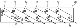
- the light source device according to the present embodiment is different from the light source device 80 according to the first embodiment in the inclination angle of the laser device 10 with respect to the arrangement direction of the plurality of laser devices 10.
- FIG. 11 is a plan view showing the light source device according to the present embodiment.
- the light source device 580 according to the present embodiment includes a substrate 82 and a plurality of laser devices 10 arranged and installed on the substrate 82, similarly to the light source device 80 according to the first embodiment. is doing.
- the bus bar 88 and the fixing screws 90 and 92 that electrically connect the terminal portion 20 and the terminal portion 22 are omitted.
- each of the plurality of laser devices 10 is arranged so that the longitudinal direction of the housing 16 is orthogonal to the arrangement direction of the plurality of laser devices 10. Has been.
- each of the plurality of laser devices 10 has an inclination angle in which the longitudinal direction of the housing 16 is an acute angle or an obtuse angle with respect to the arrangement direction of the plurality of laser devices 10. It is arranged to incline. That is, each laser device 10 is arranged such that the longitudinal direction of the housing 16 is inclined at a predetermined inclination angle other than 90 ° with respect to the arrangement direction of the plurality of laser devices 10.
- Each of the plurality of laser devices 10 arranged so as to be inclined is attached and fixed on the installation surface of the substrate 82 in the same manner as the laser device 10 of the light source device 80 according to the first embodiment.
- each of the plurality of laser devices 10 is arranged such that the longitudinal direction of the casing 16 of the laser device 10 is inclined at an acute angle or an obtuse angle with respect to the arrangement direction of the plurality of laser devices 10. May be.
- a laser device according to a ninth embodiment of the present invention will be described with reference to FIGS. Note that the same components as those of the laser device and the light source device according to the first to eighth embodiments are denoted by the same reference numerals, and description thereof is omitted or simplified.
- the basic configuration of the laser apparatus according to the present embodiment is the same as that of the laser apparatus 10 according to the first embodiment.
- the laser apparatus according to the present embodiment further includes an electronic component different from the semiconductor laser element 12 and a terminal portion corresponding thereto.
- FIG. 12 is an exploded perspective view showing the laser apparatus according to the present embodiment.
- FIG. 13 is an enlarged perspective view showing electronic components in the laser apparatus according to the present embodiment.
- the laser device 610 includes an electronic component 612 and corresponding terminal portions 614 and 616 in addition to the configuration of the laser device 10 according to the first embodiment. is doing.
- the electronic component 612 is accommodated in the housing 16. Further, as will be described later, portions of the terminal portions 614 and 616 other than the portion protruding outside the housing 16 are also accommodated in the housing 16.
- the electronic component 612 is different from the semiconductor laser element 12 and is, for example, a temperature sensor such as a thermistor for detecting the temperature in the housing 16.
- the electronic component 612 is installed on a region near the output unit 18 of the bottom plate unit 24.
- the electronic component 612 is installed on the bottom plate portion 24 in the form of a COS that is fixedly mounted on the submant 618 by soldering or the like, for example.
- the bottom plate portion 24 is expanded as compared with the first embodiment because the electronic component 612 and the terminal portions 614 and 616 are provided.
- the electronic component 612 is not limited to a temperature sensor.
- the electronic component 612 may be a photodetector such as a photodiode, for example.
- the terminal portions 614 and 616 corresponding to the electronic component 612 are respectively installed on the bottom plate portion 24 in the vicinity of the electronic component 612 in the housing 16.
- the terminal portions 614 and 616 are electrically connected to an external circuit portion corresponding to the electronic component 612, respectively, to realize the function of the electronic component 612.
- the electronic component 612 is a temperature sensor such as a thermistor
- the terminal portions 614 and 616 are connected to predetermined terminals of the temperature measuring circuit, and temperature measurement by the temperature sensor is realized.
- the terminal portions 614 and 616 each have a component connection portion 620 and an external connection portion 622 electrically connected to the component connection portion 620.
- Each of the terminal portions 614 and 616 is of a connection type using a screw for electrical connection with the outside.
- the component connection part 620 and the external connection part 622 of the terminal parts 614 and 616 have the same structure as the element connection part 44 and the external connection part 46 of the terminal parts 20 and 22, respectively.
- the component connecting portions 620 of the terminal portions 614 and 616 are provided on the bottom plate portion 24. As described above, the component connecting portion 620 that is a part of each of the terminal portions 614 and 616 is provided on the bottom plate portion 24.
- the component connecting portions 620 of the terminal portions 614 and 616 have sheet-like conductors 624, respectively.
- the sheet-like conductor 624 is provided in parallel to the bottom plate portion 24.
- the sheet-like conductor 624 is electrically connected to the electrode of the electronic component 612 via, for example, a wire by wire bonding.
- the sheet-like conductor 624 of the component connecting portion 620 in the terminal portion 614 is electrically connected to one electrode of the electronic component 612 via a wire by wire bonding.
- the sheet-like conductor 624 of the component connection portion 620 in the terminal portion 616 is electrically connected to the other electrode of the electronic component 612 via a wire by wire bonding.
- the method of electrically connecting the sheet-like conductor 624 of the component connecting portion 620 and the electrode of the electronic component 612 is not limited to the method by wire bonding, and various methods can be used.
- the external connection part 622 of each terminal part 614, 616 is provided on the component connection part 620.
- the external connection portion 622 of each of the terminal portions 614 and 616 includes a columnar conductor 626 formed in a columnar shape that is perpendicular to the bottom plate portion 24, for example.
- the columnar conductor 626 is electrically connected to the sheet-like conductor 624.
- Each columnar conductor 626 has a female screw hole 628 at its upper end that opens upward. Each female screw hole 628 is used for electrical connection with the outside, as will be described later.
- the external connection portions 622 of the terminal portions 614 and 616 are provided upward with respect to the bottom plate portion 24 in the same manner as the external connection portions 46 of the terminal portions 20 and 22. That is, the external connection portion 622 that is a part of each of the terminal portions 614 and 616 is provided so as to extend in the direction opposite to the installation surface on the side opposite to the installation surface on which the bottom plate portion 24 is installed and fixed. ing.
- Opening portions 630 and 632 are provided in the top plate portion 36 of the lid portion 26 corresponding to the external connection portions 622 of the terminal portions 614 and 616, respectively.
- the external connection portions 622 of the terminal portions 614 and 616 partially protrude above the top plate portion 36, that is, outside the housing 16 through openings 630 and 632 provided in the top plate portion 36, respectively.
- the external connection portions 622 of the terminal portions 614 and 616 partially protrude from the upper surface of the housing 16 to the outside of the housing 16.
- Each external connection portion 622 partially protruding outside the housing 16 has the female screw hole 628 facing upward.
- the lid portion 26 is expanded compared to the first embodiment to accommodate the expanded bottom plate portion 24 in order to accommodate the electronic component 612 and the terminal portions 614 and 616 in the housing 16.
- the external connection portions 622 of the terminal portions 614 and 616 can be electrically connected to the outside using screws or screw portions that are screwed into the female screw holes 628.
- a bus bar that is a conductor rod is fixed to the external connection portion 622 while being in contact with the columnar conductor 626 by a screw that is screwed into the female screw hole 628, and the external connection portion 622 is electrically connected to the outside via the fixed bus bar.
- an external terminal having a male screw part that is screwed into the female screw hole 628 is used, the male screw part of the external terminal is screwed into the female screw hole 628 and fixed, and the external connection part 622 is electrically connected to the outside via the fixed external terminal. Can be connected.
- an external terminal which is a round or tip-open crimp terminal, is fixed to the external connection portion 622 while being brought into contact with the columnar conductor 626 by an external thread that is screwed into the internal thread hole 628, and the fixed external terminal is interposed therebetween.
- the external connection portion 622 can be electrically connected to the outside.
- an electronic component 612 and terminal portions 614 and 616 corresponding to the electronic component 612 may be further provided.
- the terminal portions 614 and 616 corresponding to the electronic component 612 are also provided upward with respect to the bottom plate portion 24 installed on the installation surface of the substrate. For this reason, like the terminal parts 20 and 22, when comprising a light source device, it is not necessary to ensure the space of the terminal parts 614 and 616, and the footprint of a light source device can be reduced. Thereby, space saving can be realized.
- the terminal portions 614 and 616 also have female screw holes 628 and are electrically connected to the outside by screws. For this reason, it is not necessary to solder the terminal portions 614 and 616 as in the case of the lead pins, and good workability can be ensured when electrically connecting to the outside.
- an electronic component 612 and terminal portions 614, 616 may be provided.
- terminal portions 614 and 616 corresponding to the electronic component 612 may be provided outside the housing 16 similarly to the terminal portions 320 and 322 in the sixth embodiment. Further, the terminal portions 614 and 616 corresponding to the electronic component 612 may be of a connection type using an opening as in the case of the terminal portions 420 and 422 in the seventh embodiment.
- the laser devices 10, 101, 102, 103, 210, 310, 410, and 610 have a plurality of semiconductor laser elements 12 has been described as an example, but the present invention is not limited to this.
- the laser devices 10, 101, 102, 103, 210, 310, 410, 610 may have one semiconductor laser element 12.
- the terminal portions 20, 22, 320, and 322 have the female screw holes 52 and 352
- the terminal portions 20, 22, 320, and 322 may have male screw portions for electrical connection with the outside instead of the female screw holes 52 and 352.
- the external terminal that is in contact with the male screw portion by an annular portion or the like inserted into the male screw portion can be fixed to the terminal portions 20, 22, 320, and 322. it can.
- the terminal portions 614 and 616 corresponding to the electronic component 612 may be those having a male screw portion.
- connection type using a screw or an opening part was demonstrated as an example as the terminal parts 20, 22, 320, 322, 420, 422, it is not limited to these, A connection type can be used.
- a connection type using a jack into which a plug such as a banana plug can be inserted can be used as the terminal portions 20, 22, 320, 322, 420, and 422, a connection type using a jack into which a plug such as a banana plug can be inserted can be used.
- the terminal portions 614 and 616 corresponding to the electronic component 612 can be of other connection types.
- the case where the plurality of laser devices 10 and 210 are installed on the substrates 82 and 282 is described as an example, but the present invention is not limited to this.
- the plurality of laser devices 10 and 210 can be installed on the installation surface of various base members such as an installation table in addition to the substrates 82 and 282.
- the several laser apparatus 10 arranged in a row demonstrated the case where the output part 18 was orient
- the present invention is not limited to this.
- a plurality of laser devices 10 arranged in a row may alternately direct the output units 18 on one side and the other side with respect to the arrangement.
- the terminal portions 20 and 22 to be connected by the bus bar 88 in the two adjacent laser devices 10 are located on the same side, the length of the bus bar 88 can be shortened, and thus the electrical connection path Can be shortened.
- the light source device 80 is used as an excitation light source for the optical fiber laser 94 as an example.
- the light source device 80 can be used as a light source for various devices or systems, such as a device that performs wavelength synthesis and a device that performs polarization synthesis.
- the light source device 80 can be used as a direct diode laser.
- the light source device 80 can be used with an optical system to which laser beams output from the plurality of laser devices 10 are incident.
- the optical system includes a lens such as a condenser lens, a combiner, a mirror, and the like.
- the laser beams output from the plurality of laser devices 10 in the light source device 80 can be collected and output by an optical system including a lens. Further, the laser beams output from the plurality of laser devices 10 in the light source device 80 can be combined and output by a combiner.
- the plurality of laser devices 10 in the light source device 80 may have the same or different laser characteristics such as the wavelength of the laser beam. The laser characteristics of the plurality of laser devices 10 can be appropriately set according to the use of the light source device 80.
Landscapes
- Physics & Mathematics (AREA)
- Optics & Photonics (AREA)
- General Physics & Mathematics (AREA)
- Electromagnetism (AREA)
- Condensed Matter Physics & Semiconductors (AREA)
- Engineering & Computer Science (AREA)
- Plasma & Fusion (AREA)
- Semiconductor Lasers (AREA)
- Optical Couplings Of Light Guides (AREA)
- Lasers (AREA)
Abstract
組立性が良好で安価に製造することができるレーザ装置及びこれを用いた光源装置を提供する。レーザ装置は、底板部と、底板部上に設置された半導体レーザ素子と、半導体レーザ素子が設置された底板部上に設けられ、天板部を有する蓋部と、底板部と天板部との間の空間の側方の一部又は全部を覆う側壁部とを有し、天板部が、側壁部の一部又は全部と一体的に形成されている。
Description
本発明は、半導体レーザ素子を有するレーザ装置、及び複数のレーザ装置を有する光源装置に関する。
半導体レーザは、消費電力が小さい、小型である等の特徴を有しており、光通信、光記録、物質加工等の様々な分野において広く利用されるに至っている。半導体レーザが実装された半導体レーザモジュールとしては、パッケージ内に複数の半導体レーザが設けられたものが知られている(特許文献1)。
従来の半導体レーザモジュールでは、パッケージの筐体内に、半導体レーザ素子やレンズ等の光学素子が収容される。パッケージの筐体の側壁部には、リードピン等の電極を含む端子部や光ファイバを含む出力部が設けられている。このように筐体の側壁部に設けられた端子部の電極は、筐体内に収容される半導体レーザ素子と電気的に接続する必要がある。また、筐体の側壁部に設けられた出力部の光ファイバは、筐体内に収容される半導体レーザ素子から出力されて光学素子による反射や集光を経たレーザ光に対して調芯を行う必要がある。
上述のように、従来の半導体レーザモジュールでは、筐体の側壁部に設けられた部材に対して、筐体内に収容される半導体レーザ素子等を電気的に接続したり、光学的に位置合わせしたりする必要がある。このため、従来の半導体レーザモジュールは、組立性が良好ではなく、よって安価に製造することが困難であった。
本発明の目的は、上記に鑑みてなされたものであって、組立性が良好で安価に製造することができるレーザ装置及びこれを用いた光源装置を提供することにある。
本発明の一観点によれば、底板部と、前記底板部上に設置された半導体レーザ素子と、前記半導体レーザ素子が設置された前記底板部上に設けられ、天板部を有する蓋部と、前記底板部と前記天板部との間の空間の側方の一部又は全部を覆う側壁部とを有し、前記天板部が、前記側壁部の一部又は全部と一体的に形成されていることを特徴とするレーザ装置が提供される。
本発明の他の観点によれば、上記の複数のレーザ装置と、前記複数のレーザ装置が設置された設置面を有するベース部材とを有することを特徴とする光源装置が提供される。
本発明のさらに他の観点によれば、上記の光源装置と、増幅用光ファイバと、前記光源装置の前記複数のレーザ装置から出力されるレーザ光を前記増幅用光ファイバに入射させる入射部とを有することを特徴とする光ファイバレーザが提供される。
本発明によれば、組立性が良好で安価に製造することができるレーザ装置及びこれを用いた光源装置を提供することができる。
[第1実施形態]
本発明の第1実施形態によるレーザ装置及び光源装置について図1A乃至図3を用いて説明する。
本発明の第1実施形態によるレーザ装置及び光源装置について図1A乃至図3を用いて説明する。
まず、本実施形態によるレーザ装置の構成について図1A及び図1Bを用いて説明する。図1Aは、本実施形態によるレーザ装置を示す斜視図である。図1Bは、本実施形態によるレーザ装置を示す分解斜視図である。
本実施形態によるレーザ装置は、レーザ素子として複数の半導体レーザ素子を有する半導体レーザモジュールである。図1A及び図1Bに示すように、本実施形態によるレーザ装置10は、複数の半導体レーザ素子12と、複数の半導体レーザ素子12に対応して設けられた光学系14を有している。また、本実施形態によるレーザ装置10は、複数の半導体レーザ素子12、光学系14等を収容するパッケージの筐体16を有している。さらに、本実施形態によるレーザ装置10は、レーザ光が出力される出力部18と、それぞれ外部と電気的に接続可能な端子部20、22とを有している。
筐体16は、例えば扁平な略直方体状の形状を有し、底板部24と、蓋部26とを有している。蓋部26は、筐体16の長手方向において互いに対向する前側壁部28及び後側壁部30と、筐体16の短手方向において互いに対向する左側壁部32及び右側壁部34とを有している。さらに、蓋部26は、底板部24に対向するように各側壁部28、30、32、34上に設けられた天板部36を有している。蓋部26は、内部空間を空けて、底板部24の底面上に設けられた複数の半導体レーザ素子12、光学系14等を覆うように底板部24上に固定されている。蓋部26は、筐体16内への塵埃の侵入を防止する防塵機能、並びに筐体16外への光の漏出及び筐体16内への光の侵入を遮断する遮光機能を有している。なお、筐体16の形状は、特に限定されるものではなく、種々の形状を採用することができる。
蓋部26において、天板部36は、前側壁部28、後側壁部30、左側壁部32及び右側壁部34の各側壁部と一体的に形成されている。すなわち、天板部36と、前側壁部28、後側壁部30、左側壁部32及び右側壁部34の各側壁部との間には、例えば溶接、接着、ねじ止め等による接合部や継ぎ目がなく、天板部36と各側壁部とが一体になっている。なお、前側壁部28と左側壁部32及び右側壁部34との間にも、例えば溶接、接着、ねじ止め等による接合部や継ぎ目がない。また、後側壁部30と左側壁部32及び右側壁部34との間にも、例えば溶接、接着、ねじ止め等による接合部や継ぎ目がなく、前側壁部28、後側壁部30、左側壁部32及び右側壁部34の各側壁部も互いに一体になっている。こうして、蓋部26は、天板部36と、前側壁部28、後側壁部30、左側壁部32及び右側壁部34のそれぞれとが一体的に形成されたものとなっている。
天板部36と一体的に形成された前側壁部28、後側壁部30、左側壁部32及び右側壁部34は、それぞれ底板部24と天板部36との間の空間の前側、後側、左側及び右側の側方を覆っている。こうして、天板部36と一体的に形成された各側壁部により、底板部24と天板部36との間の空間の側方の全部が覆われている。
上記のように天板部36と各側壁部とが一体的に形成された蓋部26は、例えば、射出成形、切削加工、鋳造法、塑性加工等により形成することができる。より具体的には、射出成形としては、例えば、金属粉末射出成形(Metal Injection Molding、MIM)、樹脂射出成形を用いることができる。また、鋳造法としては、例えばダイカスト法を用いることができる。また、塑性加工としては、例えば、曲げ加工、絞り加工等のプレス加工を用いることができる。なお、蓋部26を形成する方法は、これらに限定されるものではない。蓋部26は、その他の種々の方法を用いて形成することができる。
なお、蓋部26においては、底板部24と天板部36との間の空間の側方の全部を覆うように前側壁部28、後側壁部30、左側壁部32及び右側壁部34が天板部36と一体的に形成されている必要はない。天板部36と一体的に形成された側壁部は、底板部24と天板部36との間の空間の側方の少なくとも一部を覆うものであればよい。
また、天板部36は、底板部24と天板部36との間の空間の側方の全部を覆う側壁部である前側壁部28、後側壁部30、左側壁部32及び右側壁部34の全部と一体的に形成されている必要はない。天板部36は、底板部24と天板部36との間の空間の側方の一部又は全部を覆う側壁部の一部又は全部と一体的に形成されていればよい。
例えば、前側壁部28、後側壁部30、左側壁部32及び右側壁部34のうちの一部が、天板部36ではなく底板部24に設けられていてもよい。また、前側壁部28、後側壁部30、左側壁部32及び右側壁部34のうちの一部が設けられておらず、天板部36と底板部24との間の空間の側方の一部が開放されていてもよい。これらの場合については、第2乃至第4実施形態において詳述する。
筐体16を構成する底板部24及び蓋部26を構成する材料は、互いに同種の材料であっても互いに異種の材料であってもよく、例えば金属であっても樹脂であってもよい。例えば、底板部24を金属で構成する一方、蓋部26を樹脂で構成することができる。ただし、底板部24を構成する材料は、蓋部26を構成する材料、すなわち互いに一体的に形成された天板部36、前側壁部28、後側壁部30、左側壁部32及び右側壁部34を構成する材料よりも熱伝導率が高いことが好ましい。すなわち、底板部24の熱伝導が、蓋部26の熱伝導率よりも高いことが好ましい。このように、発熱する半導体レーザ素子12が後述のように設けられる底板部24の熱伝導率を比較的に高くする一方、蓋部26の熱伝導率を底板部24の熱伝導率よりも低くすることで、製品コストの上昇を抑制しつつ、優れた放熱特性を得ることができる。
蓋部26は、例えば、接着剤、ねじ止め、はんだ付け等により底板部24上に固定されている。こうして底板部24上に蓋部26が固定された筐体16は、ハーメチックシールが施されておらず、気密封止されていない状態になっている。
筐体16内には、複数の半導体レーザ素子12、光学系14及び後述の集光レンズ64が収容されている。また、筐体16内には、後述するように端子部20、22の筐体16外に突出した部分以外の部分が収容されている。
底板部24は、後述するように、レーザ装置10を基板上に設置する際に、基板の設置面上にその下面を接触させて設置される部分である。底板部24上には、段差部38が設けられている。段差部38は、階段状になっており、筐体16の前後方向に沿って並ぶように設けられた複数の段40を有している。段差部38の複数の段40は、前方から後方に向かうに従って段々に高くなっている。段差部38は、底板部24と一体的に形成されていてもよいし、はんだ付け等により底板部24に固定された別部品であってもよい。なお、上述のように、底板部24の熱伝導率を蓋部26の熱伝導率よりも高くすることができる。これにより、製品コストの上昇を抑制しつつ、優れた放熱特性を得ることができる。
底板部24上及び段差部38の複数の段40上には、複数の半導体レーザ素子12が設置されている。複数の半導体レーザ素子12は、例えば、互いに発振波長、出力その他のレーザ特性を同じくする同一の半導体レーザ素子である。なお、複数の半導体レーザ素子12の数は、特に限定されるものではなく、レーザ装置10に要求されるレーザ出力等に応じて適宜設定することができる。
複数の半導体レーザ素子12は、別々のチップに形成された互いに別個独立の素子である。各半導体レーザ素子12は、例えば、サブマント42上にはんだ付け等により固定されて搭載されたチップオンサブマウント(Chip On Submount、COS)の形態で、底板部24上及び段差部38の複数の段40上に設置されている。
底板部24上及び段差部38の複数の段40上に設置された複数の半導体レーザ素子12は、筐体16の長手方向に沿って一列に配列されている。一列に配列された複数の半導体レーザ素子12の間には、段差部38による高低差が設けられている。複数の半導体レーザ素子12は、それぞれレーザ光の出力方向が筐体16の短手方向になるように配置されている。一列に配列された複数の半導体レーザ素子12は、その配列に対して同じ一方の側にレーザ光を出力するように配置されている。なお、複数の半導体レーザ素子12の配列は、一列のみならず、複数列設けられていてもよい。
複数の半導体レーザ素子12の配列においては、隣接する半導体レーザ素子12の電極がワイヤボンディング等により電気的に接続されている。これにより、複数の半導体レーザ素子12が直列に接続されている。なお、半導体レーザ素子12を電気的に接続する方法は、特に限定されるものではなく、種々の方法を用いることができるが、例えば特開2015-185667号公報に記載されるワイヤボンディングによる方法を用いることができる。
複数の半導体レーザ素子12の配列の前方側において、筐体16内の底板部24上には、端子部20が設けられている。また、複数の半導体レーザ素子12の配列の後方側において、筐体16内の底板部24上には、端子部22が設けられている。端子部20、22は、それぞれ外部の駆動電源に電気的に接続可能であり、駆動電源により複数の半導体レーザ素子12のそれぞれに駆動電流を印加するためのものである。端子部20、22のうち、一方が駆動電源の正極端子に接続され、他方が駆動電源の負極端子に接続される。
端子部20、22は、それぞれ、素子接続部44と、素子接続部44と電気的に接続された外部接続部46とを有している。端子部20、22は、それぞれ外部との電気的な接続に際してねじを利用する接続形式のものである。
各端子部20、22の素子接続部44は、底板部24上に設けられている。このように、各端子部20、22の一部である素子接続部44が、底板部24に設けられている。各端子部20、22の素子接続部44は、シート状導体48をそれぞれ有している。シート状導体48は、底板部24に平行に設けられている。シート状導体48は、直列に接続された複数の半導体レーザ素子12の配列における端部の半導体レーザ素子12の電極に、例えばワイヤボンディングによるワイヤを介して電気的に接続されている。
より具体的には、端子部20における素子接続部44のシート状導体48は、直列に接続された複数の半導体レーザ素子12の配列における前側の端部の半導体レーザ素子12の電極に、ワイヤボンディングによるワイヤを介して電気的に接続されている。また、端子部22における素子接続部44のシート状導体48は、直列に接続された複数の半導体レーザ素子12の配列における後側の端部の半導体レーザ素子12の電極に、ワイヤボンディングによるワイヤを介して電気的に接続されている。なお、素子接続部44のシート状導体48と半導体レーザ素子12の電極とを電気的に接続する方法は、ワイヤボンディングによる方法に限定されるものではなく、種々の方法を用いることができる。
各端子部20、22の外部接続部46は、素子接続部44上に設けられている。各端子部20、22の外部接続部46は、例えば底板部24に垂直な柱状に形成された柱状導体50を有している。各端子部20、22において、柱状導体50は、シート状導体48に電気的に接続されている。各柱状導体50は、上方に向けて開口した雌ねじ孔52を上端に有している。各雌ねじ孔52は、後述するように、外部との電気的な接続のために用いられるものである。こうして、各端子部20、22の外部接続部46は、底板部24に対して上向きに設けられている。すなわち、各端子部20、22の一部である外部接続部46は、底板部24が設置されて固定される設置面とは反対側において、その設置面と反対方向に延伸するように設けられている。なお、底板部24に対して上向きとは、底板部24に直交する方向に底板部24に対して上向きである場合のほか、底板部24に直交する方向に対して所定の傾斜角度で傾斜する方向に底板部24に対して上向きである場合をも含みうる。すなわち、底板部24に対して上向く方向は、底板部24に直交する方向のみならず、底板部24に直交する方向に対して所定の傾斜角度で傾斜する方向であってもよい。
蓋部26の天板部36には、端子部20、22の外部接続部46にそれぞれ対応して開口部54、56が設けられている。端子部20、22の外部接続部46は、それぞれ天板部36に設けられた開口部54、56を介して、天板部36の上方、すなわち筐体16の外部に部分的に突出している。こうして、端子部20、22の外部接続部46は、それぞれ筐体16の上面から筐体16の外部に部分的に突出している。筐体16の外部に部分的に突出した各外部接続部46は、雌ねじ孔52を上方に向けている。
各端子部20、22の外部接続部46は、雌ねじ孔52に螺合するねじ又はねじ部を利用して、外部と電気的に接続することができる。例えば、雌ねじ孔52に螺合するねじにより、導体棒であるバスバーを、柱状導体50と接触させつつ外部接続部46に固定し、固定したバスバーを介して外部接続部46を外部と電気的に接続することができる。また、雌ねじ孔52に螺合する雄ねじ部を有する外部端子を用い、外部端子の雄ねじ部を雌ねじ孔52に螺合して固定し、固定した外部端子を介して外部接続部46を外部と電気的に接続することができる。また、例えば丸形又は先開形の圧着端子である外部端子を、雌ねじ孔52に螺合する雄ねじにより、柱状導体50と接触させつつ外部接続部46に固定し、固定した外部端子を介して外部接続部46を外部と電気的に接続することができる。
複数の半導体レーザ素子12の配列の一方の側には、光学系14が設けられている。光学系14は、複数組のコリメートレンズ58、60及び反射ミラー62を有している。複数組のコリメートレンズ58、60及び反射ミラー62は、複数の半導体レーザ素子12に対応して、底板部24上及び段差部38の複数の段40上に設置されている。複数のコリメートレンズ58は、光学特性を同じくする同一のものになっている。複数のコリメートレンズ60は、光学特性を同じくする同一のものになっている。複数の反射ミラー62は、光学特性を同じくする同一のものになっている。
コリメートレンズ58、60及び反射ミラー62の各組において、コリメートレンズ58、60は、対応する半導体レーザ素子12のレーザ光の出力側に順次配置されている。また、反射ミラー62は、コリメートレンズ60の後段に配置されている。コリメートレンズ58、60は、対応する半導体レーザ素子12から出力されたレーザ光をそれぞれ縦方向及び横方向にコリメートして平行光とする。反射ミラー62は、対応するコリメートレンズ58、60によりコリメートされたレーザ光を前方側に90°反射して、出力部18が設けられた筐体16の前方側に導く。
底板部24の前方端部上には、出力部18が設けられている。出力部18と光学系14との間には、集光レンズ64が設けられている。蓋部26の前側壁部28には、出力部18が嵌合する切り欠き部66が設けられている。出力部18は、レーザ光を出力するための光ファイバ68を有しており、光ファイバ68を通してレーザ光を出力するようになっている。なお、光ファイバ68の長さは、設計に応じて適宜変更することができる。
出力部18の光ファイバ68は、筐体16の内部に固定された一端である固定端と、筐体16の外部に引き出された一端である出力端とを有している。集光レンズ64は、光学系14とともに、複数の半導体レーザ素子12から出力されたレーザ光を光ファイバ68の固定端に入射させるための光学系を構成している。集光レンズ64は、複数の反射ミラー62のそれぞれにより反射されたレーザ光を、光ファイバ68の固定端に集光して入射させる。光ファイバ68の固定端に入射したレーザ光は、光ファイバ68を伝搬して、レーザ装置10の出力として光ファイバ68の出力端から出力される。なお、光ファイバ68の固定端にレーザ光を入射させるための光学系の構成は、集光レンズ64を含む複数枚の集光レンズを有するものであってもよいし、各種フィルタを有するものであってもよい。
また、底板部24の前端部及び後端部には、固定ねじが貫通する貫通孔70、72がそれぞれ設けられている。貫通孔70、72は、互いに対角に位置している。蓋部26の天板部36には、底板部24に設けられた貫通孔70、72に対応して、固定ねじが貫通する貫通孔74、76がそれぞれ設けられている。
本実施形態によるレーザ装置10は、後述するように、例えば、基板上に複数配列されて光源装置として用いられる。レーザ装置10が配列される基板の設置面には、雄ねじである固定ねじが螺合する雌ねじ孔が設けられている。レーザ装置10は、貫通孔70、74を貫通して基板に設けられた雌ねじ孔に螺合する固定ねじ、及び貫通孔72、76を貫通して基板に設けられた雌ねじ孔に螺合する固定ねじにより、基板の設置面上に取り付けられて固定される。なお、レーザ装置10を基板の設置面上に固定する方法は、特に限定されるものではなく、固定ねじを用いた方法のほか、ボルト及びナットを用いた方法、接着剤を用いた方法等の種々の方法を用いることができる。
こうして、本実施形態によるレーザ装置10が構成されている。
本実施形態によるレーザ装置10の動作時には、端子部20、22に電気的に接続された外部の駆動電源により、直列に接続された複数の半導体レーザ素子12のそれぞれに駆動電流が印加される。駆動電流が印加されると、各半導体レーザ素子12は、レーザ発振してレーザ光を出力する。各半導体レーザ素子12から出力されたレーザ光は、対応するコリメートレンズ58、60によりコリメートされた後、対応する反射ミラー62により反射されて集光レンズ64に導かれる。各反射ミラー62により反射されたレーザ光は、集光レンズ64により集光されて出力部18の光ファイバ68の固定端に入射する。光ファイバ68の固定端に入射したレーザ光は、レーザ装置10の出力として、光ファイバ68の出力端から出力される。
本実施形態によるレーザ装置10は、上述のように、蓋部26において、天板部36が、前側壁部28、後側壁部30、左側壁部32及び右側壁部34の各側壁部と一体的に形成されている。一方、半導体レーザ素子12の電極に電気的に接続される端子部20、22は、底板部24上に設けられている。また、レーザ光を出力するための光ファイバ68を含む出力部18も、底板部24上に設けられている。このため、本実施形態によるレーザ装置10では、そのパッケージの組み立てに際して、筐体16の側壁部に設けられた部材に対して、筐体16内に収容される半導体レーザ素子12を電気的に接続したり、光学的に位置合わせしたりする必要がない。天板部36と各側壁部とが互いに一体的に形成された蓋部26は、底板部24上に単に固定するだけでよい。したがって、本実施形態によるレーザ装置10は、組立性が良好で安価に製造することができる。
さらに、本実施形態によるレーザ装置10では、端子部20、22が、雌ねじ孔52を有しており、ねじにより外部と電気的に接続されるようになっている。このため、本実施形態によるレーザ装置10によれば、リードピンのようにはんだ付けをする必要がない。したがって、本実施形態によるレーザ装置10によれば、外部との電気的な接続に際して良好な作業性を確保することができる。
また、本実施形態によるレーザ装置10では、端子部20、22の外部接続部46が、天板部36の上方、すなわち筐体16の外部に部分的に突出している。このように外部接続部46が突出していることにより、本実施形態によるレーザ装置10によれば、例えば接続作業が容易なバスバーの利用が可能である等、外部との電気的な接続を高い作業性で行うことができる。
さらに、本実施形態によるレーザ装置10は、高価なハーメチックシールが施されたリードピンを用いる必要がない。したがって、本実施形態によるレーザ装置10によれば、より安価な価格を実現することができる。
このように、本実施形態によれば、組立性が良好で安価に製造することができるレーザ装置10を実現することができる。
本実施形態によるレーザ装置10は、これを複数配列することにより光源装置を構成することができる。複数のレーザ装置10を用いることにより、光源装置の高出力化を図ることができる。以下、複数のレーザ装置10を配列した本実施形態による光源装置について図2A及び図2Bを用いて説明する。図2Aは、本実施形態による光源装置を示す斜視図である。図2Bは、本実施形態による光源装置を示す平面図である。
図2A及び図2Bに示すように、本実施形態による光源装置80は、基板82と、基板82上に配列されて設置された複数のレーザ装置10とを有している。なお、複数のレーザ装置10の数は、特に限定されるものではなく、光源装置80に要求されるレーザ出力等に応じて適宜設定することができる。
基板82は、配列される複数のレーザ装置10が設置された設置面を有し、その設置面上に設置された複数のレーザ装置10を支持するベース部材である。基板82の設置面上には、複数のレーザ装置10のそれぞれが、底板部24側を基板82側にして取り付けられて固定されている。各レーザ装置10は、上述のように、貫通孔70、74を貫通して基板82の雌ねじ孔に螺合する固定ねじ84、及び貫通孔72、76を貫通して基板82の雌ねじ孔に螺合する固定ねじ86により、基板82の設置面上に取り付けられて固定されている。
基板82の設置面上に設置された複数のレーザ装置10は、例えば基板82の長手方向を配列方向として横方向に一列に配列されている。一列に配列された複数のレーザ装置10は、その配列に対して同じ側に出力部18を向けている。複数のレーザ装置10のそれぞれは、複数のレーザ装置10の配列方向に対して、その筐体16の長手方向が直交するように配置されている。なお、配列方向に対するレーザ装置10の傾斜角度は、特に限定されるものではなく、適宜設定することができる。
隣接する2つのレーザ装置10のうち、一方のレーザ装置10の端子部20と、他方のレーザ装置10の端子部22とは、導体棒であるバスバー88により電気的に接続されている。バスバー88の一端は、一方のレーザ装置10の端子部20の雌ねじ孔52に螺合する固定ねじ90により、その端子部20に固定されて端子部20に電気的に接続されている。バスバー88の他端は、他方のレーザ装置10の端子部22の雌ねじ孔52に螺合する固定ねじ92により、その端子部22に固定されて端子部22に電気的に接続されている。こうして、複数のレーザ装置10が直列に接続されている。なお、複数のレーザ装置10を電気的に接続する方法は、バスバー88を用いた方法に限定されるものではなく、リード線を用いた方法等の種々の方法を用いることができる。
こうして、本実施形態による光源装置80が構成されている。
上述のように、本実施形態によるレーザ装置10は安価に製造することができるため、複数のレーザ装置10を用いた光源装置80も安価に製造することができる。
また、本実施形態によるレーザ装置10は、上述のように、外部と電気的に接続可能な端子部20、22が、基板82の設置面上に設置される底板部24に対して上向きに設けられている。このため、複数のレーザ装置10を例えば図2A及び図2Bに示すように横方向に配列して光源装置80を構成する場合に、端子部20、22のスペースを確保する必要がなく、光源装置80のフットプリントを低減することができる。これにより、省スペース化を実現することができる。
本実施形態による光源装置80は、例えば、光ファイバレーザの励起光源として用いることができる。ここで、本実施形態による光源装置80を励起光源として用いた光ファイバレーザについて図3を用いて説明する。図3は、本実施形態による光源装置80を励起光源として用いた光ファイバレーザを示す概略図である。
図3に示すように、本実施形態による光源装置80を励起光源として用いた光ファイバレーザ94は、励起光源としての光源装置80と、光結合部としてのポンプコンバイナ96とを有している。また、光ファイバレーザ94は、増幅用光ファイバとしての希土類添加光ファイバ98と、出力側光ファイバ100とを有している。希土類添加光ファイバ98の入力端及び出力端には、それぞれ高反射FBG(Fiber Bragg Grating)102及び低反射FBG104が設けられている。
光源装置80に含まれる複数のレーザ装置10における出力部18の光ファイバ68の出力端は、複数入力1出力のポンプコンバイナ96の複数の入力ポートにそれぞれ結合されている。ポンプコンバイナ96の出力ポートには、希土類添加光ファイバ98の入力端が接続されている。希土類添加光ファイバ98の出力端には、出力側光ファイバ100の入力端が接続されている。なお、複数のレーザ装置10から出力されるレーザ光を希土類添加光ファイバ98に入射させる入射部としては、ポンプコンバイナ96に代えて他の構成を用いることもできる。例えば、複数のレーザ装置10における出力部18の光ファイバ68を並べて配置し、複数の光ファイバ68から出力されたレーザ光を、レンズを含む光学系等の入射部を用いて、希土類添加光ファイバ98の入力端に入射させるように構成してもよい。
こうして、本実施形態による光源装置80を励起光源として用いた光ファイバレーザ94が構成されている。
光ファイバレーザ94において、複数のレーザ装置10の光ファイバ68から出力されたレーザ光は、ポンプコンバイナ96により結合されてその出力ポートから出力される。入射部としてのポンプコンバイナ96は、その出力ポートから出力された励起光としてのレーザ光を、希土類添加光ファイバ98の入力端に入射させる。希土類添加光ファイバ98においては、高反射FBG102及び低反射FBG104により、希土類添加光ファイバ98を含む共振器が形成されている。
増幅用光ファイバである希土類添加光ファイバ98では、伝搬する励起光が、コアにドープされた希土類元素に吸収されて、基底準位と準安定準位との間に反転分布が生じて光が放出される。こうして放出された光は、希土類添加光ファイバ98の光増幅作用と高反射FBG102及び低反射FBG104により構成されるレーザ共振器の作用とによってレーザ発振する。こうして、レーザ発振によりレーザ光が生じる。生じたレーザ光は、希土類添加光ファイバ98の出力端に接続された出力側光ファイバ100の出力端から出力される。
[第2実施形態]
本発明の第2実施形態によるレーザ装置及び光源装置について図4A及び図4Bを用いて説明する。なお、上記第1実施形態によるレーザ装置及び光源装置と同様の構成要素については同一の符号を付し説明を省略し又は簡略にする。
本発明の第2実施形態によるレーザ装置及び光源装置について図4A及び図4Bを用いて説明する。なお、上記第1実施形態によるレーザ装置及び光源装置と同様の構成要素については同一の符号を付し説明を省略し又は簡略にする。
本実施形態によるレーザ装置の基本的構成は、第1実施形態によるレーザ装置10の構成と同様である。本実施形態によるレーザ装置は、第1実施形態によるレーザ装置10の蓋部26における前側壁部28、後側壁部30、左側壁部32及び右側壁部34のうちの一部が、天板部36と一体的に形成されているのではなく、底板部24に設けられている。この点で、本実施形態によるレーザ装置は、第1実施形態によるレーザ装置10とは異なっている。
図4Aは、本実施形態によるレーザ装置を示す斜視図である。図4Bは、本実施形態によるレーザ装置を示す分解斜視図である。図4A及び図4Bに示すように、本実施形態によるレーザ装置101では、蓋部26において、天板部36が、前側壁部28、後側壁部30及び左側壁部32と一体的に形成されている。一方、蓋部26において、第1実施形態の右側壁部34に相当する側壁部は設けられていない。なお、本実施形態の蓋部26も、第1実施形態の蓋部26と同様に、例えば、射出成形、切削加工、鋳造法、塑性加工等により形成することができる。
一方、底板部24の右側端部には、第1実施形態の右側壁部34に相当する右側壁部35が設けられている。右側壁部35は、底板部24と一体的に形成されていてもよいし、例えば接着剤、ねじ止め等により底板部24に固定された底板部24とは別個のものであってもよい。右側壁部35が底板部24と一体的に形成されている場合、一体的に形成された底板部24及び右側壁部35は、蓋部26と同様に、例えば、射出成形、切削加工、鋳造法、塑性加工等により形成することができる。
このように、本実施形態では、天板部36が、側壁の一部である前側壁部28、後側壁部30及び左側壁部32と一体的に形成されている一方、側壁部の他の一部である右側壁部34が底板部24に設けられている。
天板部36と前側壁部28、後側壁部30及び左側壁部32とが一体的に形成された蓋部26は、内部空間を空けて、複数の半導体レーザ素子12、光学系14等を覆うように、右側壁部35が設けられた底板部24上に固定されている。底板部24と天板部36との間の空間の側方は、天板部36と一体的に形成された前側壁部28、後側壁部30、左側壁部32、並びに底板部24に設けられた右側壁部35により全部覆われている。
こうして、本実施形態によるレーザ装置101では、天板部36と前側壁部28、後側壁部30及び左側壁部32とが一体的に形成された蓋部26と、右側壁部35が設けられた底板部24とにより筐体16が構成されている。
なお、本実施形態によるレーザ装置101においても、第1実施形態と同様に、底板部24の熱伝導率を蓋部26の熱伝導率よりも高くすることができる。すなわち、底板部24及びこれと一体的に形成された右側壁部35を構成する材料は、蓋部26を構成する材料、すなわち互いに一体的に形成された天板部36、前側壁部28、後側壁部30及び左側壁部32を構成する材料よりも熱伝導率が高いことが好ましい。これにより、製品コストの上昇を抑制しつつ、優れた放熱特性を得ることができる。
本実施形態のように、筐体16を構成する側壁部のうちの一部が、蓋部26ではなく、底板部24に設けられていてもよい。
[第3実施形態]
本発明の第3実施形態によるレーザ装置及び光源装置について図5A及び図5Bを用いて説明する。なお、上記第1及び第2実施形態によるレーザ装置及び光源装置と同様の構成要素については同一の符号を付し説明を省略し又は簡略にする。
本発明の第3実施形態によるレーザ装置及び光源装置について図5A及び図5Bを用いて説明する。なお、上記第1及び第2実施形態によるレーザ装置及び光源装置と同様の構成要素については同一の符号を付し説明を省略し又は簡略にする。
本実施形態によるレーザ装置の基本的構成は、第1実施形態によるレーザ装置10の構成と同様である。本実施形態によるレーザ装置は、第1実施形態によるレーザ装置10の蓋部26において天板部36と一体的に形成されていた前側壁部28、後側壁部30、左側壁部32及び右側壁部34のうちの一部が設けられていない。この点で、本実施形態によるレーザ装置は、第1実施形態によるレーザ装置10とは異なっている。
図5Aは、本実施形態によるレーザ装置を示す斜視図である。図5Bは、本実施形態によるレーザ装置を示す分解斜視図である。図5A及び図5Bに示すように、本実施形態によるレーザ装置102では、蓋部26において、天板部36が、左側壁部32及び右側壁部34と一体的に形成されている。一方、蓋部26において、第1実施形態の前側壁部28及び後側壁部30に相当する側壁部は設けられていない。なお、本実施形態の蓋部26も、第1実施形態の蓋部26と同様に、例えば、射出成形、切削加工、鋳造法、塑性加工等により形成することができる。
天板部36と左側壁部32及び右側壁部34とが一体的に形成された蓋部26は、内部空間を空けて、複数の半導体レーザ素子12、光学系14等を覆うように、底板部24上に固定されている。底板部24と天板部36との間の空間の側方の一部である前側の側方及び後側の側方は、側壁部に覆われておらず、開放された状態になっている。
こうして、本実施形態によるレーザ装置102では、天板部36と左側壁部32及び右側壁部34とが一体的に形成された蓋部26と、底板部24とにより筐体16が構成されている。筐体16の一部が開放されているため、本実施形態によるレーザ装置102では、より優れた放熱特性を得ることができる。
なお、本実施形態によるレーザ装置102においても、第1実施形態と同様に、底板部24の熱伝導率を蓋部26の熱伝導率よりも高くすることができる。すなわち、底板部24を構成する材料は、蓋部26を構成する材料、すなわち互いに一体的に形成された天板部36、左側壁部32及び右側壁部34を構成する材料よりも熱伝導率が高いことが好ましい。これにより、製品コストの上昇を抑制しつつ、優れた放熱特性を得ることができる。
本実施形態のように、筐体16を構成する側壁部のうちの一部が設けられておらず、筐体16の一部が開放されていてもよい。
なお、上記では、第1実施形態によるレーザ装置10と同様の構成において、前側壁部28及び後側壁部30が設けられていない場合について説明したが、これに限定されるものではない。第2実施形態によるレーザ装置101と同様の構成においても、前側壁部28及び後側壁部30を設けないようにすることができる。
[第4実施形態]
本発明の第4実施形態によるレーザ装置及び光源装置について図6A及び図6Bを用いて説明する。なお、上記第1乃至第3実施形態によるレーザ装置及び光源装置と同様の構成要素については同一の符号を付し説明を省略し又は簡略にする。
本発明の第4実施形態によるレーザ装置及び光源装置について図6A及び図6Bを用いて説明する。なお、上記第1乃至第3実施形態によるレーザ装置及び光源装置と同様の構成要素については同一の符号を付し説明を省略し又は簡略にする。
本実施形態によるレーザ装置の基本的構成は、第1実施形態によるレーザ装置10の構成と同様である。本実施形態によるレーザ装置は、前側壁部28、後側壁部30、左側壁部32及び右側壁部34の各側壁部の下側部分が、底板部24に設けられている。この点で、本実施形態によるレーザ装置は、第1実施形態によるレーザ装置10とは異なっている。
図6Aは、本実施形態によるレーザ装置を示す斜視図である。図6Bは、本実施形態によるレーザ装置を示す分解斜視図である。図6A及び図6Bに示すように、本実施形態によるレーザ装置103では、前側壁部28は、底板部24側の下側部分28aと、天板部36側の上側部分28bとから構成されている。また、後側壁部30は、底板部24側の下側部分30aと、天板部36側の上側部分30bとから構成されている。また、左側壁部32は、底板部24側の下側部分32aと、天板部36側の上側部分32bとから構成されている。また、右側壁部34は、底板部24側の下側部分34aと、天板部36側の上側部分34bとから構成されている。
蓋部26においては、天板部36が、前側壁部28の上側部分28b、後側壁部30の上側部分30b、左側壁部32の上側部分32b及び右側壁部34の上側部分34bと一体的に形成されている。なお、本実施形態の蓋部26も、第1実施形態の蓋部26と同様に、例えば、射出成形、切削加工、鋳造法、塑性加工等により形成することができる。
底板部24には、前側壁部28の下側部分28a、後側壁部30の下側部分30a、左側壁部32の下側部分32a及び右側壁部34の下側部分34aがそれぞれ設けられている。下側部分28a、下側部分30a、下側部分32a及び下側部分34aは、底板部24と一体的に形成されていてもよいし、例えば接着剤、ねじ止め等により底板部24に固定された底板部24とは別個のものであってもよい。下側部分28a、30a、32a、34aが底板部24と一体的に形成されている場合、一体的に形成された底板部24及び各下側部分は、蓋部26と同様に、例えば、射出成形、切削加工、鋳造法、塑性加工等により形成することができる。
前側壁部28の上側部分28bは、前側壁部28の下側部分28aに固定されている。後側壁部30の上側部分30bは、後側壁部30の下側部分30aに固定されている。左側壁部32の上側部分32bは、左側壁部32の下側部分32aに固定されている。右側壁部34の上側部分34bは、右側壁部34の下側部分34aに固定されている。これら各側壁部の上側部分と下側部分とは、例えば接着剤等により固定されている。
なお、本実施形態によるレーザ装置102においても、第1実施形態と同様に、底板部24の熱伝導率を蓋部26の熱伝導率よりも高くすることができる。すなわち、底板部24及びこれに設けられた各側壁部の下側部分を構成する材料は、蓋部26を構成する材料、すなわち互いに一体的に形成された天板部36及び各側壁部の上側部分を構成する材料よりも熱伝導率が高いことが好ましい。これにより、製品コストの上昇を抑制しつつ、優れた放熱特性を得ることができる。
本実施形態のように、前側壁部28の上側部分28b、後側壁部30の上側部分30b、左側壁部32の上側部分32b及び右側壁部34の上側部分34bが天板部36と一体的に形成されてもよい。
なお、上記では、第1実施形態によるレーザ装置10と同様の構成において、各側壁部が下側部分と上側部分とから構成される場合について説明したが、これに限定されるものではない。第2及び第3実施形態によるレーザ装置101、102と同様の構成においても、各側壁部が下側部分と上側部分とから構成されるようにすることができる。
[第5実施形態]
本発明の第5実施形態によるレーザ装置及び光源装置について図7及び図8を用いて説明する。なお、上記第1乃至第4実施形態によるレーザ装置及び光源装置と同様の構成要素については同一の符号を付し説明を省略し又は簡略にする。
本発明の第5実施形態によるレーザ装置及び光源装置について図7及び図8を用いて説明する。なお、上記第1乃至第4実施形態によるレーザ装置及び光源装置と同様の構成要素については同一の符号を付し説明を省略し又は簡略にする。
本実施形態によるレーザ装置の基本的構成は、第1実施形態によるレーザ装置10の構成と同様である。本実施形態によるレーザ装置は、レーザ装置10を基板の設置面上に取り付けて固定するための底板部24の貫通孔70、72及び天板部36の貫通孔74、76に代えて固定部を有する点で、第1実施形態によるレーザ装置10とは異なっている。
図7は、本実施形態によるレーザ装置を示す斜視図である。図7に示すように、本実施形態によるレーザ装置210は、筐体16の底板部24に設けられた複数の固定部212を有している。なお、本実施形態によるレーザ装置210では、第1実施形態によるレーザ装置10とは異なり、底板部24には貫通孔70、72は設けられておらず、天板部36にも貫通孔74、76は設けられていない。
各固定部212は、底板部24から筐体16の外側に突出するように底板部24に設けられている。例えば、底板部24の長手方向に沿った2つの縁端部のうち、一方に2つに固定部212が設けられ、他方に1つの固定部212が設けられている。なお、固定部212の数及び位置は、特に限定されるものではなく、適宜変更することができる。
各固定部212には、固定ねじが貫通する貫通孔214が設けられている。レーザ装置210は、レーザ装置10と同様に、例えば、基板の設置面上に複数配列されて光源装置として用いられる。レーザ装置210が配列される基板の設置面には、雄ねじである固定ねじが螺合する雌ねじ孔が設けられている。レーザ装置210は、各固定部212の貫通孔214を貫通して基板の設置面に設けられた雌ねじ孔に螺合する固定ねじにより、基板の設置面上に取り付けられて固定される。なお、レーザ装置210を基板の設置面上に固定する方法は、特に限定されるものではなく、固定ねじを用いた方法のほか、ボルト及びナットを用いた方法等の種々の方法を用いることができる。
図8は、本実施形態による光源装置を示す平面図である。図8に示すように、本実施形態による光源装置280は、基板282と、基板282上に配列されて設置された複数のレーザ装置210とを有している。なお、図8では、端子部20と端子部22との間を電気的に接続するバスバー88及び固定ねじ90、92を省略している。
基板282上には、複数のレーザ装置210のそれぞれが、底板部24側を基板282側にして取り付けられている。各レーザ装置210は、上述のように、各固定部212に設けられた貫通孔214を貫通して基板282の雌ねじ孔に螺合する固定ねじ216により、基板282の設置面上に取り付けられて固定されている。
本実施形態のように、レーザ装置210を基板282の設置面上に取り付けて固定するための固定部212が、筐体16の外側に設けられていてもよい。
なお、上記では、第1実施形態によるレーザ装置10と同様の構成において、貫通孔70、72、74、76に代えて固定部212を有する場合について説明したが、これに限定されるものではない。第2及び第3実施形態によるレーザ装置101、102と同様の構成においても、貫通孔70、72、74、76に代えて固定部212を有するように構成することができる。
[第6実施形態]
本発明の第6実施形態によるレーザ装置について図9を用いて説明する。なお、上記第1乃至第5実施形態によるレーザ装置及び光源装置と同様の構成要素については同一の符号を付し説明を省略し又は簡略にする。
本発明の第6実施形態によるレーザ装置について図9を用いて説明する。なお、上記第1乃至第5実施形態によるレーザ装置及び光源装置と同様の構成要素については同一の符号を付し説明を省略し又は簡略にする。
本実施形態によるレーザ装置の基本的構成は、第5実施形態によるレーザ装置210の構成と同様である。本実施形態によるレーザ装置は、端子部20、22に代えて、筐体16の外部に設けられた端子部を有している点で、第5実施形態によるレーザ装置210とは異なっている。
図9は、本実施形態によるレーザ装置を示す斜視図である。図9に示すように、本実施形態によるレーザ装置310は、端子部20、22に代えて、筐体16の外部に設けられた端子部320、322を有している。
端子部320は、蓋部26の前側壁部28に設けられている。端子部322は、蓋部26の後側壁部30に設けられている。端子部320、322は、外部と電気的に接続可能であり、それぞれ端子部20、22と同様の機能を有するものである。
端子部320、322は、それぞれ、素子接続部344と、素子接続部344と電気的に接続された外部接続部346とを有している。端子部320、322は、それぞれ外部との電気的な接続に際してねじを利用する接続形式のものである。
端子部320の素子接続部344は、蓋部26の前側壁部28を内外に貫通するように底板部24に平行に設けられている。端子部320の素子接続部344は、上記シート状導体48と同様の不図示のシート状導体を有している。このシート状導体は、複数の半導体レーザ素子12の配列における前側の端部の半導体レーザ素子12の電極に、ワイヤボンディングによるワイヤを介して電気的に接続されている。
端子部322の素子接続部344は、蓋部26の後側壁部30を内外に貫通するように底板部24に平行に設けられている。端子部322の素子接続部344は、上記シート状導体48と同様の不図示のシート状導体を有している。このシート状導体は、複数の半導体レーザ素子12の配列における後側の端部の半導体レーザ素子12の電極に、ワイヤボンディングによるワイヤを介して電気的に接続されている。
なお、各素子接続部344のシート状導体と半導体レーザ素子12の電極とを電気的に接続する方法は、ワイヤボンディングによる方法に限定されるものではなく、種々の方法を用いることができる。
各端子部320、322の外部接続部346は、素子接続部344の筐体16外の部分上に設けられている。各端子部320、322の外部接続部346は、例えば底板部24に垂直な柱状に形成された柱状導体350をそれぞれ有している。各端子部320、322において、柱状導体350は、素子接続部344のシート状導体に電気的に接続されている。各柱状導体350は、上方に向けて開口した雌ねじ孔352を上端に有している。こうして、各端子部320、322の外部接続部346は、第1実施形態における各端子部20、22の外部接続部46と同様に、底板部24に対して上向きに設けられている。すなわち、各端子部320、322の一部である外部接続部346は、底板部24が設置されて固定される設置面とは反対側において、その設置面と反対方向に延伸するように設けられている。
各端子部320、322の外部接続部346は、上記端子部20、22の外部接続部46と同様に、雌ねじ孔352に螺合するねじ又はねじ部を利用して、外部と電気的に接続することができる。
本実施形態のように、外部と電気的に接続可能な端子部320、322が、筐体16の外部に設けられていてもよい。
なお、上記では、第5実施形態によるレーザ装置210と同様の構成において、端子部20、22に代えて端子部320、322を設ける場合について説明したが、これに限定されるものではない。第1乃至第4実施形態によるレーザ装置10と同様の構成においても、端子部20、22に代えて端子部320、322を設けることができる。
[第7実施形態]
本発明の第7実施形態によるレーザ装置について図10を用いて説明する。なお、上記第1乃至第6実施形態によるレーザ装置及び光源装置と同様の構成要素については同一の符号を付し説明を省略し又は簡略にする。
本発明の第7実施形態によるレーザ装置について図10を用いて説明する。なお、上記第1乃至第6実施形態によるレーザ装置及び光源装置と同様の構成要素については同一の符号を付し説明を省略し又は簡略にする。
本実施形態によるレーザ装置の基本的構成は、第5実施形態によるレーザ装置210の構成と同様である。本実施形態によるレーザ装置は、端子部20、22に代えて、端子部20、22とは形状及び外部との接続形式が異なる端子部を有している点で、第5実施形態によるレーザ装置210とは異なっている。
図10は、本実施形態によるレーザ装置を示す斜視図である。図10に示すように、本実施形態によるレーザ装置410は、端子部20、22に代えて端子部420、422を有している。
端子部420、422は、それぞれ端子部20、22と同様の機能を有するものである。ただし、端子部420、422は、端子部20、22とは形状及び外部との接続形式が異なっている。すなわち、端子部420、422は、それぞれ外部との電気的な接続に際して、以下に説明する開口部448を利用する接続形式のものである。
端子部420、422は、それぞれ蓋部26の天板部36から上方に向かって、筐体16の外部に突出する外部接続部446を有している。各外部接続部446は、筐体16の上面から筐体16の外部に部分的に突出している。各外部接続部446は、筐体16の長手方向に直交する板状導体で構成されている。各外部接続部446には、筐体16の長手方向に沿って貫通する開口部448が設けられている。なお、各外部接続部446は、筐体16内において、素子接続部44と同様の素子接続部と電気的に接続されている。
端子部420、422の外部接続部446には、それぞれ開口部448を利用して外部端子を電気的に接続することができる。例えば、丸形又は先開形の圧着端子である外部端子を、外部接続部446の側方から、開口部448に通したボルト及び対応するナットにより外部接続部446に固定することができる。このようにして、外部端子を端子部420、422にそれぞれ電気的に接続することができる。
本実施形態のように、ねじを利用する接続形式の端子部20、22に代えて、開口部448を利用する接続形式の端子部420、422が設けられていてもよい。
なお、上記では、第5実施形態によるレーザ装置210と同様の構成において、端子部20、22に代えて端子部420、422を設ける場合について説明したが、これに限定されるものではない。第1乃至第4実施形態によるレーザ装置10、101、102、103と同様の構成においても、端子部20、22に代えて端子部420、422を設けることができる。また、第6実施形態によるレーザ装置310と同様の構成においても、端子部320、322に代えて端子部420、422を設けることができる。
[第8実施形態]
本発明の第8実施形態による光源装置について図11を用いて説明する。なお、上記第1乃至第7実施形態によるレーザ装置及び光源装置と同様の構成要素については同一の符号を付し説明を省略し又は簡略にする。
本発明の第8実施形態による光源装置について図11を用いて説明する。なお、上記第1乃至第7実施形態によるレーザ装置及び光源装置と同様の構成要素については同一の符号を付し説明を省略し又は簡略にする。
本実施形態による光源装置の基本的構成は、第1実施形態による光源装置80の構成と同様である。本実施形態による光源装置は、複数のレーザ装置10の配列方向に対するレーザ装置10の傾斜角度が、第1実施形態による光源装置80とは異なっている。
図11は、本実施形態による光源装置を示す平面図である。図11に示すように、本実施形態による光源装置580は、第1実施形態による光源装置80と同様に、基板82と、基板82上に配列されて設置された複数のレーザ装置10とを有している。なお、図11では、端子部20と端子部22との間を電気的に接続するバスバー88及び固定ねじ90、92を省略している。
第1実施形態による光源装置80においては、上述のように、複数のレーザ装置10のそれぞれは、複数のレーザ装置10の配列方向に対して、その筐体16の長手方向が直交するように配置されている。
これに対して、本実施形態による光源装置580において、複数のレーザ装置10のそれぞれは、複数のレーザ装置10の配列方向に対して、その筐体16の長手方向が鋭角又は鈍角の傾斜角度で傾斜するように配置されている。すなわち、各レーザ装置10は、複数のレーザ装置10の配列方向に対して、その筐体16の長手方向が90°以外の所定の傾斜角度で傾斜するように配置されている。
なお、傾斜するように配置された複数のレーザ装置10のそれぞれは、第1実施形態による光源装置80のレーザ装置10と同様に、基板82の設置面上に取り付けられて固定されている。
本実施形態のように、複数のレーザ装置10の配列方向に対してレーザ装置10の筐体16の長手方向が鋭角又は鈍角の傾斜角度で傾斜するように、複数のレーザ装置10のそれぞれが配置されていてもよい。
[第9実施形態]
本発明の第9実施形態によるレーザ装置について図12及び図13を用いて説明する。なお、上記第1乃至第8実施形態によるレーザ装置及び光源装置と同様の構成要素については同一の符号を付し説明を省略し又は簡略にする。
本発明の第9実施形態によるレーザ装置について図12及び図13を用いて説明する。なお、上記第1乃至第8実施形態によるレーザ装置及び光源装置と同様の構成要素については同一の符号を付し説明を省略し又は簡略にする。
本実施形態によるレーザ装置の基本的構成は、第1実施形態によるレーザ装置10の構成と同様である。本実施形態によるレーザ装置は、第1実施形態によるレーザ装置10の構成に加えて、さらに半導体レーザ素子12とは異なる電子部品及びこれに対応する端子部を有している。
図12は、本実施形態によるレーザ装置を示す分解斜視図である。図13は、本実施形態によるレーザ装置における電子部品を示す拡大斜視図である。
図12及び図13に示すように、本実施形態によるレーザ装置610は、第1実施形態によるレーザ装置10の構成に加えて、電子部品612と、これに対応する端子部614、616とを有している。
電子部品612は、筐体16内に収容されている。また、後述するように端子部614、616の筐体16外に突出した部分以外の部分も、筐体16内に収容されている。
電子部品612は、半導体レーザ素子12とは異なるものであり、例えば、筐体16内の温度を検出するサーミスタ等の温度センサである。電子部品612は、底板部24の出力部18近傍の領域上に設置されている。電子部品612は、例えば、サブマント618上にはんだ付け等により固定されて搭載されたCOSの形態で、底板部24上に設置されている。底板部24は、電子部品612及び端子部614、616を設けるため、第1実施形態と比較して拡張されている。
なお、電子部品612は、温度センサに限定されるものではない。電子部品612は、例えば、フォトダイオード等の光検出器であってもよい。
電子部品612に対応する端子部614、616は、筐体16内において、それぞれ底板部24の電子部品612の近傍の領域上に設置されている。端子部614、616は、それぞれ電子部品612に応じた外部の回路部に電気的に接続され、電子部品612の機能を実現するためのものである。電子部品612がサーミスタ等の温度センサである場合、端子部614、616はそれぞれ測温回路の所定の端子に接続されて、温度センサによる温度測定が実現される。
端子部614、616は、それぞれ、部品接続部620と、部品接続部620と電気的に接続された外部接続部622とを有している。端子部614、616は、それぞれ外部との電気的な接続に際してねじを利用する接続形式のものである。端子部614、616の部品接続部620及び外部接続部622は、それぞれ端子部20、22の素子接続部44及び外部接続部46と同様の構造を有している。
各端子部614、616の部品接続部620は、底板部24上に設けられている。このように、各端子部614、616の一部である部品接続部620が、底板部24に設けられている。各端子部614、616の部品接続部620は、シート状導体624をそれぞれ有している。シート状導体624は、底板部24に平行に設けられている。シート状導体624は、電子部品612の電極に、例えばワイヤボンディングによるワイヤを介して電気的に接続されている。
より具体的には、端子部614における部品接続部620のシート状導体624は、電子部品612の一方の電極に、ワイヤボンディングによるワイヤを介して電気的に接続されている。また、端子部616における部品接続部620のシート状導体624は、電子部品612の他方の電極に、ワイヤボンディングによるワイヤを介して電気的に接続されている。なお、部品接続部620のシート状導体624と電子部品612の電極とを電気的に接続する方法は、ワイヤボンディングによる方法に限定されるものではなく、種々の方法を用いることができる。
各端子部614、616の外部接続部622は、部品接続部620上に設けられている。各端子部614、616の外部接続部622は、例えば底板部24に垂直な柱状に形成された柱状導体626を有している。各端子部614、616において、柱状導体626は、シート状導体624に電気的に接続されている。各柱状導体626は、上方に向けて開口した雌ねじ孔628を上端に有している。各雌ねじ孔628は、後述するように、外部との電気的な接続のために用いられるものである。こうして、各端子部614、616の外部接続部622は、端子部20、22の外部接続部46と同様に、底板部24に対して上向きに設けられている。すなわち、各端子部614、616の一部である外部接続部622は、底板部24が設置されて固定される設置面とは反対側において、その設置面と反対方向に延伸するように設けられている。
蓋部26の天板部36には、端子部614、616の外部接続部622にそれぞれ対応して開口部630、632が設けられている。端子部614、616の外部接続部622は、それぞれ天板部36に設けられた開口部630、632を介して、天板部36の上方、すなわち筐体16の外部に部分的に突出している。こうして、端子部614、616の外部接続部622は、それぞれ筐体16の上面から筐体16の外部に部分的に突出している。筐体16の外部に部分的に突出した各外部接続部622は、雌ねじ孔628を上方に向けている。なお、蓋部26は、電子部品612及び端子部614、616を筐体16内に収容するため、拡張された底板部24に対応して第1実施形態と比較して拡張されている。
各端子部614、616の外部接続部622は、雌ねじ孔628に螺合するねじ又はねじ部を利用して、外部と電気的に接続することができる。例えば、雌ねじ孔628に螺合するねじにより、導体棒であるバスバーを、柱状導体626と接触させつつ外部接続部622に固定し、固定したバスバーを介して外部接続部622を外部と電気的に接続することができる。また、雌ねじ孔628に螺合する雄ねじ部を有する外部端子を用い、外部端子の雄ねじ部を雌ねじ孔628に螺合して固定し、固定した外部端子を介して外部接続部622を外部と電気的に接続することができる。また、例えば丸形又は先開形の圧着端子である外部端子を、雌ねじ孔628に螺合する雄ねじにより、柱状導体626と接触させつつ外部接続部622に固定し、固定した外部端子を介して外部接続部622を外部と電気的に接続することができる。
本実施形態のように、電子部品612及びこれに対応する端子部614、616がさらに設けられていてもよい。この場合において、電子部品612に対応する端子部614、616も、基板の設置面上に設置される底板部24に対して上向きに設けられている。このため、端子部20、22と同様に、光源装置を構成する場合に端子部614、616のスペースを確保する必要がなく、光源装置のフットプリントを低減することができる。これにより、省スペース化を実現することができる。
また、端子部614、616も、雌ねじ孔628を有しており、ねじにより外部と電気的に接続されるようになっている。このため、端子部614、616についても、リードピンのようにはんだ付けをする必要がなく、外部との電気的な接続に際して良好な作業性を確保することができる。
なお、上記では、第1実施形態によるレーザ装置10の構成に加えて電子部品612及び端子部614、616が設けられている場合について説明したが、これに限定されるものではない。第2乃至第7実施形態によるレーザ装置101、102、103、210、310、410の構成に加えて、電子部品612及び端子部614、616が設けられていてもよい。
また、電子部品612に対応する端子部614、616は、第6実施形態における端子部320、322と同様に、筐体16の外部に設けられていてもよい。また、電子部品612に対応する端子部614、616は、第7実施形態における端子部420、422と同様に、開口部を利用する接続形式のものであってもよい。
[変形実施形態]
本発明は、上記実施形態に限らず、種々の変形が可能である。
本発明は、上記実施形態に限らず、種々の変形が可能である。
例えば、上記実施形態では、レーザ装置10、101、102、103、210、310、410、610が複数の半導体レーザ素子12を有する場合を例に説明したが、これに限定されるものではない。レーザ装置10、101、102、103、210、310、410、610は、1つの半導体レーザ素子12を有するものであってもよい。
また、上記実施形態では、端子部20、22、320、322が雌ねじ孔52、352を有する場合を例に説明したが、これに限定されるものではない。端子部20、22、320、322は、雌ねじ孔52、352に代えて、外部との電気的な接続のための雄ねじ部を有するものとすることができる。この場合、例えば、その雄ねじ部に螺合するナット等を用いて、雄ねじ部に挿入された環状部等により雄ねじ部と接触した外部端子を端子部20、22、320、322に固定することができる。電子部品612に対応する端子部614、616についても、同様に雄ねじ部を有するものを用いることができる。
また、上記実施形態では、端子部20、22、320、322、420、422としてねじ又は開口部を利用する接続形式のものを例に説明したが、これらに限定されるものではなく、他の接続形式のものを用いることができる。例えば、端子部20、22、320、322、420、422として、バナナプラグ等のプラグが挿入可能なジャックを利用する接続形式のものとすることができる。電子部品612に対応する端子部614、616についても、同様に他の接続形式のものを用いることができる。
また、上記実施形態では、複数のレーザ装置10、210を基板82、282上に設置する場合を例に説明したが、これに限定されるものではない。複数のレーザ装置10、210は、基板82、282のほか、設置台等の種々のベース部材の設置面上に設置することができる。
また、上記実施形態では、図2A及び図2Bに示すように、一列に配列された複数のレーザ装置10が、その配列に対して同じ側に出力部18を向けている場合を例に説明したが、これに限定されるものではない。例えば、一列に配列された複数のレーザ装置10が、その配列に対して一方の側と他方の側に互い違いに出力部18を向けていてもよい。この場合、隣接する2つのレーザ装置10におけるバスバー88で接続すべき端子部20、22が互いに同じ側に位置するので、バスバー88の長さを短縮することができ、よって、電気的な接続経路を短縮することができる。
また、上記実施形態では、図3に示すように、光源装置80を光ファイバレーザ94の励起光源として用いる場合を例に説明したが、これに限定されるものではない。光源装置80は、波長合成を行う装置、偏波合成を行う装置等、種々の装置又はシステムの光源として用いることができる。また、光源装置80は、ダイレクトダイオードレーザとして用いることができる。例えば、光源装置80は、その複数のレーザ装置10から出力されたレーザ光が入射される光学系とともに用いることができる。光学系には、集光レンズ等のレンズ、コンバイナ、ミラー等が含まれる。より具体的には、光源装置80における複数のレーザ装置10から出力されたレーザ光を、レンズを含む光学系により集光して出力することができる。また、光源装置80における複数のレーザ装置10から出力されたレーザ光を、コンバイナにより結合して出力することができる。なお、光源装置80における複数のレーザ装置10は、レーザ光の波長等のレーザ特性が互いに同一であっても異なっていてもよい。複数のレーザ装置10のレーザ特性は、光源装置80の用途に応じて適宜設定することができる。
10、101、102、103、210、310、410、610…レーザ装置
12…半導体レーザ素子
16…筐体
18…出力部
20、320、420…端子部
22、322、422…端子部
80、280、580…光源装置
82、282…基板
94…光ファイバレーザ
96…ポンプコンバイナ
98…希土類添加光ファイバ
612…電子部品
614…端子部
616…端子部
12…半導体レーザ素子
16…筐体
18…出力部
20、320、420…端子部
22、322、422…端子部
80、280、580…光源装置
82、282…基板
94…光ファイバレーザ
96…ポンプコンバイナ
98…希土類添加光ファイバ
612…電子部品
614…端子部
616…端子部
Claims (9)
- 底板部と、
前記底板部上に設置された半導体レーザ素子と、
前記半導体レーザ素子が設置された前記底板部上に設けられ、天板部を有する蓋部と、
前記底板部と前記天板部との間の空間の側方の一部又は全部を覆う側壁部とを有し、
前記天板部が、前記側壁部の一部又は全部と一体的に形成されていることを特徴とするレーザ装置。 - 前記天板部が、前記側壁部の前記一部と一体的に形成され、
前記側壁部の前記一部以外の他の一部が、前記底板部に設けられていることを特徴とする請求項1記載のレーザ装置。 - 前記底板部上に設けられ、前記半導体レーザ素子から出力されるレーザ光を、光ファイバを通して出力する出力部を有することを特徴とする請求項1又は2に記載のレーザ装置。
- 前記底板部に対して上向きに設けられ、外部と電気的に接続可能な端子部と
を有することを特徴とする請求項1乃至3のいずれか1項に記載のレーザ装置。 - 前記端子部の一部が、前記底板部に設けられていることを特徴とする請求項4記載のレーザ装置。
- 前記底板部の熱伝導率が、前記蓋部の熱伝導率よりも高いことを特徴とする請求項1乃至5のいずれか1項に記載のレーザ装置。
- 請求項1乃至6のいずれか1項に記載の複数のレーザ装置と、
前記複数のレーザ装置が設置された設置面を有するベース部材と
を有することを特徴とする光源装置。 - 前記複数のレーザ装置から出力されたレーザ光が入射される光学系を有することを特徴とする請求項7記載の光源装置。
- 請求項7又は8に記載の光源装置と、
増幅用光ファイバと、
前記光源装置の前記複数のレーザ装置から出力されるレーザ光を前記増幅用光ファイバに入射させる入射部と
を有することを特徴とする光ファイバレーザ。
Priority Applications (3)
| Application Number | Priority Date | Filing Date | Title |
|---|---|---|---|
| DE112017005970.4T DE112017005970T5 (de) | 2016-11-25 | 2017-11-24 | Laservorrichtung und Lichtquellenvorrichtung |
| CN201780071878.6A CN109983638B (zh) | 2016-11-25 | 2017-11-24 | 激光装置及光源装置 |
| US16/422,343 US11011885B2 (en) | 2016-11-25 | 2019-05-24 | Laser device and light-source device |
Applications Claiming Priority (2)
| Application Number | Priority Date | Filing Date | Title |
|---|---|---|---|
| JP2016-229525 | 2016-11-25 | ||
| JP2016229525A JP6844994B2 (ja) | 2016-11-25 | 2016-11-25 | レーザ装置及び光源装置 |
Related Child Applications (1)
| Application Number | Title | Priority Date | Filing Date |
|---|---|---|---|
| US16/422,343 Continuation US11011885B2 (en) | 2016-11-25 | 2019-05-24 | Laser device and light-source device |
Publications (1)
| Publication Number | Publication Date |
|---|---|
| WO2018097240A1 true WO2018097240A1 (ja) | 2018-05-31 |
Family
ID=62195064
Family Applications (1)
| Application Number | Title | Priority Date | Filing Date |
|---|---|---|---|
| PCT/JP2017/042195 Ceased WO2018097240A1 (ja) | 2016-11-25 | 2017-11-24 | レーザ装置及び光源装置 |
Country Status (5)
| Country | Link |
|---|---|
| US (1) | US11011885B2 (ja) |
| JP (1) | JP6844994B2 (ja) |
| CN (1) | CN109983638B (ja) |
| DE (1) | DE112017005970T5 (ja) |
| WO (1) | WO2018097240A1 (ja) |
Cited By (1)
| Publication number | Priority date | Publication date | Assignee | Title |
|---|---|---|---|---|
| WO2023033141A1 (ja) * | 2021-09-02 | 2023-03-09 | 古河電気工業株式会社 | 光学装置および光学装置の分解方法 |
Families Citing this family (11)
| Publication number | Priority date | Publication date | Assignee | Title |
|---|---|---|---|---|
| JP6844993B2 (ja) * | 2016-11-25 | 2021-03-17 | 古河電気工業株式会社 | レーザ装置及び光源装置 |
| EP3922626B1 (en) | 2019-02-08 | 2024-09-04 | Agc Inc. | Fluorine-containing ether compound, fluorine-containing ether composition, coating liquid, article, method for producing article, and method for producing fluorine-containing compound |
| JP7370753B2 (ja) * | 2019-07-18 | 2023-10-30 | 古河電気工業株式会社 | 光源ユニット、光源装置および光ファイバレーザ |
| CN110376689B (zh) * | 2019-07-22 | 2021-02-12 | 上海营湾医疗科技有限公司 | 光电耦合透镜组 |
| JP7760915B2 (ja) | 2019-12-26 | 2025-10-28 | Agc株式会社 | 表面処理剤、表面処理剤組成物、コーティング液、物品、及び物品の製造方法 |
| JP7407602B2 (ja) * | 2020-01-16 | 2024-01-04 | 古河電気工業株式会社 | 発光装置、光源ユニット、光源装置、および光ファイバレーザ |
| JP7612461B2 (ja) * | 2021-03-09 | 2025-01-14 | 浜松ホトニクス株式会社 | レーザ装置 |
| US11876343B2 (en) | 2021-05-18 | 2024-01-16 | Trumpf Photonics, Inc. | Laser diode packaging platforms |
| US11557874B2 (en) * | 2021-05-18 | 2023-01-17 | Trumpf Photonics, Inc. | Double-sided cooling of laser diodes |
| CN115548856B (zh) * | 2022-12-01 | 2023-04-11 | 中国科学院西安光学精密机械研究所 | 一种指向可调的激光发射光源及其调节方法与光学仪器 |
| WO2025205469A1 (ja) * | 2024-03-28 | 2025-10-02 | 古河電気工業株式会社 | 光モジュール |
Citations (7)
| Publication number | Priority date | Publication date | Assignee | Title |
|---|---|---|---|---|
| JP2001264590A (ja) * | 2000-03-17 | 2001-09-26 | Anritsu Corp | 光モジュール用パッケージ |
| JP2003338654A (ja) * | 2002-05-22 | 2003-11-28 | Furukawa Electric Co Ltd:The | 半導体レーザモジュール |
| US20090245315A1 (en) * | 2008-03-28 | 2009-10-01 | Victor Faybishenko | Laser diode assemblies |
| JP2010232373A (ja) * | 2009-03-26 | 2010-10-14 | Furukawa Electric Co Ltd:The | 光源装置 |
| JP2013239672A (ja) * | 2012-05-17 | 2013-11-28 | Panasonic Corp | ファイバレーザ発振器 |
| JP2015005627A (ja) * | 2013-06-21 | 2015-01-08 | 京セラ株式会社 | 素子収納用パッケージおよびこれを備えた実装構造体 |
| JP2016099573A (ja) * | 2014-11-25 | 2016-05-30 | 株式会社フジクラ | 光モジュールの製造方法 |
Family Cites Families (26)
| Publication number | Priority date | Publication date | Assignee | Title |
|---|---|---|---|---|
| JPS54131599A (en) | 1978-04-04 | 1979-10-12 | Shiraishi Kogyo Kaisha Ltd | Alumina composite calcium carbonate and its manufacture |
| JPS5730814A (en) | 1980-07-17 | 1982-02-19 | Olympus Optical Co Ltd | Photographic lens |
| JPH11220191A (ja) | 1998-01-29 | 1999-08-10 | Miyachi Technos Corp | 固体レーザ装置 |
| JP2001337250A (ja) * | 2000-05-25 | 2001-12-07 | Sumitomo Electric Ind Ltd | 光半導体気密封止容器及び光半導体モジュール |
| DE10204397A1 (de) * | 2001-02-02 | 2002-08-22 | Optolab Licensing Gmbh | Laserdiodenarray und Herstellverfahren dafür |
| JP2005159104A (ja) * | 2003-11-27 | 2005-06-16 | Sony Corp | レーザ・システム |
| CN201203679Y (zh) | 2007-12-27 | 2009-03-04 | 王仲明 | 一种多路半导体激光耦合入单根光纤的结构 |
| JP5415553B2 (ja) * | 2008-11-28 | 2014-02-12 | エヌケイティー フォトニクス アクティーゼルスカブ | 改良されたクラッドポンプ光導波路 |
| WO2010110068A1 (ja) * | 2009-03-25 | 2010-09-30 | 古河電気工業株式会社 | 半導体レーザモジュールおよび半導体レーザモジュールの製造方法 |
| DE102010000908B4 (de) * | 2010-01-14 | 2015-07-16 | Infineon Technologies Ag | Leistungshalbleitermodul mit niederinduktiven Hochstromkontakten, Leistungshalbleitermodulsystem, Leistungshalbleitermodulanordnung und Verfahren zur Herstellung einer Leisungshalbleitermodulanordnung |
| US8432945B2 (en) | 2010-09-30 | 2013-04-30 | Victor Faybishenko | Laser diode combiner modules |
| JP5679897B2 (ja) * | 2011-05-02 | 2015-03-04 | シチズン電子株式会社 | Ledモジュール |
| CN202383321U (zh) | 2011-12-19 | 2012-08-15 | 北京凯普林光电科技有限公司 | 一种将多路分立半导体激光耦合入单根光纤的耦合系统 |
| CN202600259U (zh) | 2012-01-16 | 2012-12-12 | 北京凯普林光电科技有限公司 | 一种将多路分立半导体激光耦合入单根光纤的耦合系统 |
| JP5772657B2 (ja) * | 2012-02-27 | 2015-09-02 | 豊田合成株式会社 | 発光モジュール |
| CN102646922A (zh) | 2012-04-26 | 2012-08-22 | 无锡亮源激光技术有限公司 | 具电路板的串联式半导体激光器 |
| JP5730814B2 (ja) | 2012-05-08 | 2015-06-10 | 古河電気工業株式会社 | 半導体レーザモジュール |
| CN102916341A (zh) | 2012-10-31 | 2013-02-06 | 中国科学院长春光学精密机械与物理研究所 | 一种单管半导体激光器合束方法 |
| JP6147341B2 (ja) | 2013-05-30 | 2017-06-14 | 古河電気工業株式会社 | 半導体レーザモジュール |
| JP6109321B2 (ja) | 2013-09-12 | 2017-04-05 | 古河電気工業株式会社 | 半導体レーザモジュール |
| JP2015185667A (ja) | 2014-03-24 | 2015-10-22 | 株式会社フジクラ | 半導体レーザモジュール、及び、半導体レーザモジュールの製造方法 |
| CN104836113A (zh) | 2015-05-18 | 2015-08-12 | 浙江合波光学科技有限公司 | 一种多单管大功率光纤耦合半导体激光器 |
| CN104836119A (zh) | 2015-05-26 | 2015-08-12 | 深圳市创鑫激光股份有限公司 | 光纤耦合激光器 |
| CN105207054B (zh) | 2015-10-14 | 2018-01-02 | 苏州大学 | 多单管半导体激光器光纤耦合模块 |
| CN205141362U (zh) | 2015-11-17 | 2016-04-06 | 山东圣达激光科技有限公司 | 一种采用双端光纤耦合输出的半导体激光器的激光系统 |
| EP3430692B1 (en) * | 2016-03-18 | 2022-05-25 | NLIGHT, Inc. | Spectrally multiplexing diode pump modules to improve brightness |
-
2016
- 2016-11-25 JP JP2016229525A patent/JP6844994B2/ja active Active
-
2017
- 2017-11-24 WO PCT/JP2017/042195 patent/WO2018097240A1/ja not_active Ceased
- 2017-11-24 DE DE112017005970.4T patent/DE112017005970T5/de active Pending
- 2017-11-24 CN CN201780071878.6A patent/CN109983638B/zh active Active
-
2019
- 2019-05-24 US US16/422,343 patent/US11011885B2/en active Active
Patent Citations (7)
| Publication number | Priority date | Publication date | Assignee | Title |
|---|---|---|---|---|
| JP2001264590A (ja) * | 2000-03-17 | 2001-09-26 | Anritsu Corp | 光モジュール用パッケージ |
| JP2003338654A (ja) * | 2002-05-22 | 2003-11-28 | Furukawa Electric Co Ltd:The | 半導体レーザモジュール |
| US20090245315A1 (en) * | 2008-03-28 | 2009-10-01 | Victor Faybishenko | Laser diode assemblies |
| JP2010232373A (ja) * | 2009-03-26 | 2010-10-14 | Furukawa Electric Co Ltd:The | 光源装置 |
| JP2013239672A (ja) * | 2012-05-17 | 2013-11-28 | Panasonic Corp | ファイバレーザ発振器 |
| JP2015005627A (ja) * | 2013-06-21 | 2015-01-08 | 京セラ株式会社 | 素子収納用パッケージおよびこれを備えた実装構造体 |
| JP2016099573A (ja) * | 2014-11-25 | 2016-05-30 | 株式会社フジクラ | 光モジュールの製造方法 |
Cited By (1)
| Publication number | Priority date | Publication date | Assignee | Title |
|---|---|---|---|---|
| WO2023033141A1 (ja) * | 2021-09-02 | 2023-03-09 | 古河電気工業株式会社 | 光学装置および光学装置の分解方法 |
Also Published As
| Publication number | Publication date |
|---|---|
| US20190280459A1 (en) | 2019-09-12 |
| JP2018085493A (ja) | 2018-05-31 |
| CN109983638A (zh) | 2019-07-05 |
| DE112017005970T5 (de) | 2019-08-01 |
| JP6844994B2 (ja) | 2021-03-17 |
| CN109983638B (zh) | 2021-04-30 |
| US11011885B2 (en) | 2021-05-18 |
Similar Documents
| Publication | Publication Date | Title |
|---|---|---|
| CN109983638B (zh) | 激光装置及光源装置 | |
| JP7247391B2 (ja) | レーザ装置及び光源装置 | |
| JP4479875B2 (ja) | 光学的サブアセンブリ | |
| US10985526B2 (en) | Laser device and light-source device | |
| TW201502628A (zh) | 光組件 | |
| US11962120B2 (en) | Semiconductor laser module | |
| JP2016115721A (ja) | 光モジュール | |
| JP2007199461A (ja) | 光モジュール | |
| CN205355526U (zh) | 一种半导体激光器单元 | |
| US7290943B2 (en) | Modular laser package system and associated methods | |
| CN112753144B (zh) | 光学半导体装置 | |
| JP2003329894A (ja) | カードエッジ型光通信モジュール及び光通信装置 | |
| JP6848161B2 (ja) | 光モジュール | |
| JP3775369B2 (ja) | レーザモジュール | |
| CN110718851B (zh) | 光学组件 | |
| JP2004281770A (ja) | 光モジュールの製造方法 | |
| JP2008015421A (ja) | 光モジュール | |
| JP2008003168A (ja) | 光モジュール | |
| WO2018110548A1 (ja) | コネクタセット及び光伝送モジュール | |
| KR20170066076A (ko) | 다중 파장을 가지는 고출력 레이저다이오드 광모듈용 서브마운트 |
Legal Events
| Date | Code | Title | Description |
|---|---|---|---|
| 121 | Ep: the epo has been informed by wipo that ep was designated in this application |
Ref document number: 17873070 Country of ref document: EP Kind code of ref document: A1 |
|
| 122 | Ep: pct application non-entry in european phase |
Ref document number: 17873070 Country of ref document: EP Kind code of ref document: A1 |