WO2018096995A1 - フレキシブル表示装置及びフレキシブル表示装置の封止方法 - Google Patents
フレキシブル表示装置及びフレキシブル表示装置の封止方法 Download PDFInfo
- Publication number
- WO2018096995A1 WO2018096995A1 PCT/JP2017/041047 JP2017041047W WO2018096995A1 WO 2018096995 A1 WO2018096995 A1 WO 2018096995A1 JP 2017041047 W JP2017041047 W JP 2017041047W WO 2018096995 A1 WO2018096995 A1 WO 2018096995A1
- Authority
- WO
- WIPO (PCT)
- Prior art keywords
- sealing film
- layer
- point metal
- display device
- melting point
- Prior art date
- Legal status (The legal status is an assumption and is not a legal conclusion. Google has not performed a legal analysis and makes no representation as to the accuracy of the status listed.)
- Ceased
Links
Images





Classifications
-
- G—PHYSICS
- G02—OPTICS
- G02F—OPTICAL DEVICES OR ARRANGEMENTS FOR THE CONTROL OF LIGHT BY MODIFICATION OF THE OPTICAL PROPERTIES OF THE MEDIA OF THE ELEMENTS INVOLVED THEREIN; NON-LINEAR OPTICS; FREQUENCY-CHANGING OF LIGHT; OPTICAL LOGIC ELEMENTS; OPTICAL ANALOGUE/DIGITAL CONVERTERS
- G02F1/00—Devices or arrangements for the control of the intensity, colour, phase, polarisation or direction of light arriving from an independent light source, e.g. switching, gating or modulating; Non-linear optics
- G02F1/01—Devices or arrangements for the control of the intensity, colour, phase, polarisation or direction of light arriving from an independent light source, e.g. switching, gating or modulating; Non-linear optics for the control of the intensity, phase, polarisation or colour
- G02F1/13—Devices or arrangements for the control of the intensity, colour, phase, polarisation or direction of light arriving from an independent light source, e.g. switching, gating or modulating; Non-linear optics for the control of the intensity, phase, polarisation or colour based on liquid crystals, e.g. single liquid crystal display cells
- G02F1/133—Constructional arrangements; Operation of liquid crystal cells; Circuit arrangements
- G02F1/1333—Constructional arrangements; Manufacturing methods
-
- G—PHYSICS
- G09—EDUCATION; CRYPTOGRAPHY; DISPLAY; ADVERTISING; SEALS
- G09F—DISPLAYING; ADVERTISING; SIGNS; LABELS OR NAME-PLATES; SEALS
- G09F9/00—Indicating arrangements for variable information in which the information is built-up on a support by selection or combination of individual elements
-
- G—PHYSICS
- G09—EDUCATION; CRYPTOGRAPHY; DISPLAY; ADVERTISING; SEALS
- G09F—DISPLAYING; ADVERTISING; SIGNS; LABELS OR NAME-PLATES; SEALS
- G09F9/00—Indicating arrangements for variable information in which the information is built-up on a support by selection or combination of individual elements
- G09F9/30—Indicating arrangements for variable information in which the information is built-up on a support by selection or combination of individual elements in which the desired character or characters are formed by combining individual elements
-
- H—ELECTRICITY
- H05—ELECTRIC TECHNIQUES NOT OTHERWISE PROVIDED FOR
- H05B—ELECTRIC HEATING; ELECTRIC LIGHT SOURCES NOT OTHERWISE PROVIDED FOR; CIRCUIT ARRANGEMENTS FOR ELECTRIC LIGHT SOURCES, IN GENERAL
- H05B33/00—Electroluminescent light sources
- H05B33/02—Details
-
- H—ELECTRICITY
- H05—ELECTRIC TECHNIQUES NOT OTHERWISE PROVIDED FOR
- H05B—ELECTRIC HEATING; ELECTRIC LIGHT SOURCES NOT OTHERWISE PROVIDED FOR; CIRCUIT ARRANGEMENTS FOR ELECTRIC LIGHT SOURCES, IN GENERAL
- H05B33/00—Electroluminescent light sources
- H05B33/02—Details
- H05B33/04—Sealing arrangements, e.g. against humidity
-
- H—ELECTRICITY
- H05—ELECTRIC TECHNIQUES NOT OTHERWISE PROVIDED FOR
- H05B—ELECTRIC HEATING; ELECTRIC LIGHT SOURCES NOT OTHERWISE PROVIDED FOR; CIRCUIT ARRANGEMENTS FOR ELECTRIC LIGHT SOURCES, IN GENERAL
- H05B33/00—Electroluminescent light sources
- H05B33/10—Apparatus or processes specially adapted to the manufacture of electroluminescent light sources
-
- H—ELECTRICITY
- H10—SEMICONDUCTOR DEVICES; ELECTRIC SOLID-STATE DEVICES NOT OTHERWISE PROVIDED FOR
- H10K—ORGANIC ELECTRIC SOLID-STATE DEVICES
- H10K59/00—Integrated devices, or assemblies of multiple devices, comprising at least one organic light-emitting element covered by group H10K50/00
- H10K59/80—Constructional details
- H10K59/87—Passivation; Containers; Encapsulations
- H10K59/871—Self-supporting sealing arrangements
- H10K59/8722—Peripheral sealing arrangements, e.g. adhesives, sealants
Definitions
- a conventional flexible display device of this type includes a gas barrier sheet (sealing film layer) covering an organic EL display layer provided on a flexible substrate, and a peripheral region of the gas barrier sheet and the substrate. Are bonded through an adhesive film (see, for example, Patent Document 1).
- thermosetting resin such as an epoxy resin or an acrylic resin is used as an adhesive film.
- these resins do not have plastic deformability, for example, a folding type Or when applied to a roll-type flexible organic EL display device, there is a problem that cracks and cracks occur. Then, once generated cracks and cracks cannot be repaired, and there is a problem of reliability such as shortening the life of the organic EL display device.
- the present invention addresses such problems, suppresses the occurrence of cracks and cracks in the peripheral region of the sealing film layer, and allows a repair of the generated cracks and cracks and a flexible display device It is an object of the present invention to provide a method for sealing an apparatus.
- a flexible display device is a flexible display device in which a display layer and a sealing film layer are laminated on a flexible substrate, and the display layer is formed on the substrate.
- a peripheral circuit portion provided in the peripheral region for driving the display layer, and a low melting point metal sealing film provided along the peripheral edge of the peripheral circuit portion and joining the substrate and the sealing film layer
- a film heater provided corresponding to the low melting point metal sealing film.
- a sealing method for a flexible display device is a sealing method for a flexible display device in which a display layer and a sealing film layer are laminated on a flexible substrate, and the display is performed on the substrate.
- the low melting point metal sealing film to be used since the low melting point metal sealing film to be used has plastic deformability, the generation of cracks in the peripheral region of the sealing film layer can be suppressed. In addition, even if cracks or cracks occur, the above-mentioned cracks or cracks can be obtained by heating the film heater provided corresponding to the low melting point metal sealing film to melt or anneal the low melting point metal sealing film. Can be repaired. Therefore, the reliability of the flexible display device can be improved.
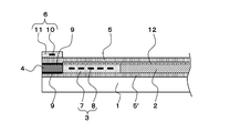
- FIG. 1 is an enlarged front view of an essential part showing a first embodiment of a flexible display device according to the present invention in section.
- a display layer and a sealing film layer are laminated on a flexible substrate.
- a film 4, a sealing film layer 5, and a film heater 6 are provided.
- the flexible display device is an organic EL display device.
- the flexible substrate 1 supports an organic EL display layer 2 which will be described later, has high barrier properties against moisture and oxygen, and has flexibility, heat resistance, etching resistance, and optical characteristics necessary for a light emitting device.
- organic EL display layer 2 which will be described later, has high barrier properties against moisture and oxygen, and has flexibility, heat resistance, etching resistance, and optical characteristics necessary for a light emitting device.
- it has a laminated structure of polyimide and polyethylene terephthalate (PET), and a known barrier film can be used.
- a peripheral circuit portion 3 is provided in the peripheral region of the organic EL display layer 2 on the flexible substrate 1.
- the peripheral circuit unit 3 is for transmitting a video signal supplied from an external drive circuit unit to each pixel of the organic EL display layer 2, and has a copper layer inside a resin layer 7 such as a polyimide film.
- a metal wiring 8 made of a good conductor such as aluminum or aluminum is formed.
- a low melting point metal sealing film 4 is provided along the peripheral edge of the peripheral circuit portion 3.
- the low melting point metal sealing film 4 is for bonding the flexible substrate 1 and a sealing film layer 5 described later, and is a film of a low melting point metal or a low melting point alloy having plastic deformability.
- the melting point of the low melting point metal sealing film 4 is preferably lower than the heat resistant temperature of the organic EL display layer 2.
- the heat resistance temperature of organic EL materials is said to be a few hundred degrees.
- the polymer organic EL material has a high heat-resistant temperature exceeding 200 ° C.
- a low melting point metal or low melting point alloy having a melting point of 200 ° C. or lower is selected as the low melting point metal sealing film 4.
- a Sn—Bi—Cu alloy has a melting point of about 170 ° C.
- a Sn—Bi—Ag alloy has a melting point of about 130 ° C.
- the low melting point metal sealing film 4 is sandwiched from the flexible substrate 1 side and the sealing film layer 5 side, and the metal film 9 having high affinity with the low melting point metal sealing film 4 (for example, Ni, Cu, etc.) ) Is desirable.
- the metal film 9 is preferably provided by being deposited or plated on the flexible substrate 1 and the sealing film layer 5 corresponding to the low melting point metal sealing film 4. Thereby, the adhesiveness of the low melting metal sealing film 4, the flexible substrate 1, and the sealing film layer 5 can be improved.
- the metal film 9 may be omitted.
- a sealing film layer 5 is laminated on the organic EL display layer 2.
- the sealing film layer 5 functions as a barrier layer that protects the organic EL display layer 2 by preventing moisture and oxygen from entering from the outside.
- a transparent resin film that transmits visible light and silicon It is formed by laminating an inorganic film such as a nitride film, and a known sealing film layer can be used.
- the sealing film layer 5 is provided so as to cover the organic EL display layer 2, the peripheral circuit portion 3, and the low melting point metal sealing film 4.
- a film heater 6 is provided on the sealing film layer 5 corresponding to the low melting point metal sealing film 4. This film heater 6 heats and melts or anneals the low melting point metal sealing film 4 even if defects such as cracks and cracks occur in the low melting point metal sealing film 4 due to stress caused by repeated bending.
- a heating resistor 10 such as a nickel alloy is sandwiched between insulating materials 11 such as a polyimide sheet. The energization of the film heater 6 may be performed after a certain period of time has elapsed from the start of use or whenever a predetermined number of bendings is reached.
- reference numeral 12 denotes a moisture adsorption film that adsorbs moisture that has entered through the sealing film layer 5 (for example, a coating-type desiccant or a sheet-type desiccant on which calcium oxide powder is adsorbed). It is provided over the layer 2.
- FIG. 2 is an enlarged front view of an essential part showing a modification of the first embodiment of the flexible display device according to the present invention.
- the organic EL display device as the flexible display device is a flexible substrate 1 in which the substrate does not have a barrier property against moisture and oxygen (non-barrier property).
- another sealing film layer 5 ′ is provided on the formation surface of the organic EL display layer 2 of the flexible substrate 1.
- the sealing film layer 5 ′ may have the same laminated structure as the sealing film layer 5 or may be completely different.
- the organic EL display layer 2 is formed in a peripheral region of the organic EL display layer 2 on the flexible substrate 1 having a barrier property against moisture and oxygen.
- a low melting point metal sealing film 4 is formed along the peripheral edge portion of the peripheral circuit portion 3 provided for driving the peripheral circuit portion 3.
- the low-melting-point metal sealing film 4 is formed by using a dispenser or an ink-jet method, screen printing, or the like, using a paste of a low-melting-point alloy such as Sn—Bi—Cu-based alloy, for example, the peripheral circuit portion 3 of the flexible substrate 1. It is applied to the peripheral part.
- a metal film 9 such as Ni or Cu having high affinity with the low melting point metal sealing film 4 is formed in advance on the flexible substrate 1 so as to correspond to the peripheral edge of the peripheral circuit section 3. It is good.
- a portion corresponding to the low melting point metal sealing film 4 is irradiated from the sealing film layer 5 side with, for example, a laser beam L to seal the low melting point metal.
- the stop film 4 is heated and melted, and the flexible substrate 1 and the sealing film layer 5 are joined by the low melting point metal sealing film 4.
- the low melting point metal sealing film 4 is formed on the surface of the sealing film layer 5 opposite to the bonding surface with the low melting point metal sealing film 4.
- the film heater 6 is attached.
- FIG. 4 shows a modification of the sealing method of the flexible display device (organic EL display device) according to the present invention.
- the film heater 6 is provided in advance on the surface opposite to the bonding surface of the sealing film layer 5 with the low melting point metal sealing film 4 so as to correspond to the low melting point metal sealing film 4. Yes.
- the organic EL is formed in the peripheral region of the organic EL display layer 2 on the flexible substrate 1 having a barrier property as in FIG.
- a low melting point metal sealing film 4 is formed along the peripheral edge portion of the peripheral circuit portion 3 provided for driving the display layer 2.
- a sealing film layer 5 in which a film heater 6 is attached in advance on the opposite surface corresponding to the low melting point metal sealing film 4 is formed into an organic EL.
- the display layer 2, the peripheral circuit portion 3 and the low melting point metal sealing film 4 are disposed so as to be covered.
- the film heater 6 is energized and heated to melt the low melting point metal sealing film 4 and the low melting point metal sealing film 4 to The sealing film layer 5 is bonded.
- the peripheral region of the sealing film layer 5 and the flexible substrate 1 are joined via the low melting point metal sealing film 4.
- higher via properties can be realized, and higher reliability can be ensured.
- the low melting point metal or low melting point alloy as the low melting point metal sealing film 4 has plastic deformability, the generation of cracks in the peripheral region of the sealing film layer of the flexible organic EL display device is suppressed. be able to.
- the repetitive bending in the foldable flexible organic EL display device as shown in FIG. Moreover, generation
- the sealing film layer 5 and the moisture absorption film 12 are not shown.
- the organic EL display layer 2 corresponds to a display unit.
- the sealing film layer 5 is made to correspond to the low-melting point metal sealing film 4.
- the cracks or cracks can be repaired by heating the provided film heater 6 to melt or anneal the low melting point metal sealing film 4.
- the reliability of the flexible organic EL display device can be further improved by performing the repair operation automatically after a predetermined time has elapsed since the start of use or whenever the number of bendings reaches a predetermined number.
- FIG. 6 is an enlarged front view of an essential part showing a cross section of a second embodiment of a flexible display device (organic EL display device) according to the present invention.
- the difference between the second embodiment and the first embodiment is that the film heater 6 is provided on the flexible substrate 1 so as to correspond to the low melting point metal sealing film 4.
- the sealing method of the second embodiment is provided in the peripheral region of the organic EL display layer 2 on the flexible substrate 1 to drive the organic EL display layer 2 as in the first embodiment.
- a first step of forming a low melting point metal sealing film 4 along the peripheral edge of the peripheral circuit portion 3 formed, and covering the organic EL display layer 2, the peripheral circuit portion 3 and the low melting point metal sealing film 4 The second step of disposing the film layer 5 and the third step of heating and melting the low melting point metal sealing film 4 to join the flexible substrate 1 side and the sealing film layer 5 are performed.
- a metal film 9 such as Ni or Cu having high affinity with the low melting point metal sealing film 4 is sandwiched between the low melting point metal sealing film 4 from the flexible substrate 1 side and the sealing film layer 5 side. It is desirable that they are arranged.
- the third step is performed by irradiating a laser beam from the sealing film layer 5 side or heating the film heater 6 to heat and melt the low melting point metal sealing film 4.
- the low melting point metal sealing film 4 can be obtained, for example, by heating the film heater 6 to melt or anneal the low melting point metal sealing film 4 after a predetermined time has elapsed from the start of use or every time the number of bending reaches a predetermined number. The operation of repairing cracks or cracks is automatically performed.
- FIG. 7 is an enlarged front view of an essential part showing a third embodiment of a flexible display device (organic EL display device) according to the present invention in section.
- the difference between the third embodiment and the first and second embodiments is that the metal film 9 provided above and below the low melting point metal sealing film 4 has the function of the film heater 6. It is a point.
- the organic EL display layer 2 is driven in the peripheral region of the organic EL display layer 2 on the flexible substrate 1 as in the first and second embodiments.
- a first step of forming a low melting point metal sealing film 4 along the peripheral edge of the peripheral circuit portion 3 provided for the purpose, and covering the organic EL display layer 2, the peripheral circuit portion 3, and the low melting point metal sealing film 4 The second step of disposing the sealing film layer 5 and the third step of joining the flexible substrate 1 side and the sealing film layer 5 by heating and melting the low melting point metal sealing film 4 are performed. is there.
- the third step is performed by irradiating laser light from the sealing film layer 5 side or heating the metal film 9 (film heater 6) to heat and melt the low melting point metal sealing film 4. Is called.
- the metal film 9 (film heater 6) is heated to melt or anneal the low melting point metal sealing film 4 after a predetermined time has elapsed since the start of use or every time the number of bendings reaches a predetermined number of times. The operation of repairing cracks or cracks in the metal sealing film 4 is automatically performed.
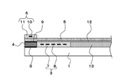
- FIG. 8 is an enlarged front view of an essential part showing a fourth embodiment of a flexible display device according to the present invention in cross section.
- the fourth embodiment is a flexible liquid crystal display device in which a liquid crystal display layer 13 and a sealing film layer 5 are laminated on a flexible substrate 1, and a liquid crystal is formed in a peripheral region of the liquid crystal display layer 13 on the flexible substrate 1.
- Peripheral circuit section 3 provided for driving display layer 13 and a low melting point metal sealing film provided along the peripheral edge of peripheral circuit section 3 and joining flexible substrate 1 and sealing film layer 5 4 and a film heater 6 provided corresponding to the low melting point metal sealing film 4.
- a sealant containing a material such as carbon fiber is used to increase mechanical strength.
- a sealing agent does not have plastic deformability, it has been difficult to apply it to a flexible display device.
Landscapes
- Physics & Mathematics (AREA)
- Nonlinear Science (AREA)
- General Physics & Mathematics (AREA)
- Engineering & Computer Science (AREA)
- Optics & Photonics (AREA)
- Crystallography & Structural Chemistry (AREA)
- Chemical & Material Sciences (AREA)
- Mathematical Physics (AREA)
- Theoretical Computer Science (AREA)
- Manufacturing & Machinery (AREA)
- Electroluminescent Light Sources (AREA)
- Devices For Indicating Variable Information By Combining Individual Elements (AREA)
- Liquid Crystal (AREA)
Abstract
本発明は、フレキシブル基板(1)上に有機EL表示層(2)と封止膜層(5)とを積層した有機EL表示装置であって、フレキシブル基板(1)上にて有機EL表示層(2)の周辺領域に有機EL表示層(2)を駆動するために設けられた周辺回路部(3)と、周辺回路部(3)の周縁部に沿って設けられ、フレキシブル基板(1)と封止膜層(5)とを接合する低融点金属封止膜(4)と、低融点金属封止膜(4)に対応して封止膜層(5)上に設けられたフィルムヒータ(6)と、を備えたものである。
Description
本発明は、可撓性の基板上に表示層と封止膜層とを積層したフレキシブル表示装置に関し、特に封止膜層の周縁領域におけるクラックやひび割れの発生を抑制すると共に、発生したクラックやひび割れの修復を可能にするフレキシブル表示装置及びフレキシブル表示装置の封止方法に係るものである。
従来の、この種のフレキシブル表示装置は、可撓性の基板上に設けられた有機EL表示層を覆ってガスバリア性シート(封止膜層)を配置し、ガスバリア性シートの周縁領域と基板とを接着剤膜を介して接着するものとなっていた(例えば、特許文献1参照)。
しかし、このような従来のフレキシブル表示装置においては、接着剤膜としてエポキシ樹脂やアクリル樹脂等の熱硬化性樹脂が使用されるが、これらの樹脂は、塑性変形性を有しないため、例えば折りたたみ式又はロール巻式のフレキシブル有機EL表示装置に適用された場合には、クラックやひび割れが発生するという問題がある。そして、一旦発生したクラックやひび割れは、修復することができず、有機EL表示装置の寿命を縮める等の信頼性の問題があった。
そこで、本発明は、このような問題点に対処し、封止膜層の周縁領域におけるクラックやひび割れの発生を抑制すると共に、発生したクラックやひび割れの修復を可能にするフレキシブル表示装置及びフレキシブル表示装置の封止方法を提供することを目的とする。
上記目的を達成するために、本発明によるフレキシブル表示装置は、可撓性の基板上に表示層と封止膜層とを積層したフレキシブル表示装置であって、前記基板上にて前記表示層の周辺領域に前記表示層を駆動するために設けられた周辺回路部と、前記周辺回路部の周縁部に沿って設けられ、前記基板と前記封止膜層とを接合する低融点金属封止膜と、前記低融点金属封止膜に対応して設けられたフィルムヒータと、を備えたものである。
また、本発明によるフレキシブル表示装置の封止方法は、可撓性の基板上に表示層と封止膜層とを積層したフレキシブル表示装置の封止方法であって、前記基板上にて前記表示層の周辺領域に、該表示層を駆動するために設けられた周辺回路部の周縁部に沿って低融点金属封止膜を形成する第1ステップと、前記表示層、前記周辺回路部及び前記低融点金属封止膜を覆って前記封止膜層を配置する第2ステップと、前記低融点金属封止膜を加熱溶融させて前記基板と前記封止膜層とを接合する第3ステップと、を実行するものである。
本発明によれば、使用する低融点金属封止膜が塑性変形性を有するために、封止膜層の周縁領域におけるクラックの発生を抑制することができる。また、例えクラックやひび割れが発生しても、低融点金属封止膜に対応して設けられたフィルムヒータを加熱して低融点金属封止膜を溶融させ又はアニールすることにより、上記クラックやひび割れを修復することができる。したがって、フレキシブル表示装置の信頼性を向上することができる。
以下、本発明の実施形態を添付図面に基づいて詳細に説明する。図1は本発明によるフレキシブル表示装置の第1の実施形態を断面で示す要部拡大正面図である。このフレキシブル表示装置は、可撓性の基板上に表示層と封止膜層とを積層したもので、フレキシブル基板1と、有機EL表示層2と、周辺回路部3と、低融点金属封止膜4と、封止膜層5と、フィルムヒータ6と、を備えて構成されている。ここでは、フレキシブル表示装置が有機EL表示装置である場合について説明する。
上記フレキシブル基板1は、後述の有機EL表示層2を支持するものであり、水分や酸素に対して高いバリア性を有すると共に、屈曲性、耐熱性、エッチング耐性,発光デバイスに必要な光学特性を有するもので、例えばポリイミドとポリエチレンテレフタレート(PET)との積層構造等であり、公知のバリアフィルムを使用することができる。
上記フレキシブル基板1の上面には、有機EL表示層2が設けられている。この有機EL表示層2は、フレキシブル基板1側から陽極、正孔輸送層、発光層、電子輸送層、陰極を積層形成した複数の画素をマトリクス状に配置したもので、外部から後述の周辺回路部3を介して供給される映像信号に応じて発光する表示層となるものである。
上記フレキシブル基板1上にて上記有機EL表示層2の周辺領域には、周辺回路部3が設けられている。この周辺回路部3は、外部に備えられた駆動回路部から供給される映像信号を上記有機EL表示層2の各画素に伝達するためのもので、ポリイミドフィルム等の樹脂層7の内部に銅やアルミニウム等の良導体の金属配線8を形成したものである。
上記周辺回路部3の周縁部に沿って低融点金属封止膜4が設けられている。この低融点金属封止膜4は、フレキシブル基板1と後述の封止膜層5とを接合するためのものであり、塑性変形性を有する低融点金属又は低融点合金の膜である。そして、低融点金属封止膜4の融点は、有機EL表示層2の耐熱温度よりも低いことが望ましい。
一般に、有機EL材料の耐熱温度は、百数十度と言われている。また、高分子有機EL材料は、200℃を超える高い耐熱温度を有している。したがって、低融点金属封止膜4としては、融点が200℃以下の低融点金属又は低融点合金が選択される。例えばSn―Bi-Cu合金は、融点が170℃程度であり、Sn―Bi-Ag合金は、融点が130℃程度である。特に、折りたたみ式のフレキシブル有機EL表示装置においては、低融点金属封止膜4として塑性変形性が特に大きいSn―Bi-Cu系合金等を選択するのが望ましい。
この場合、上記低融点金属封止膜4をフレキシブル基板1側及び封止膜層5側から挟んで、低融点金属封止膜4との親和性の高い金属膜9(例えば、NiやCu等)が配置されるのが望ましい。詳細には、上記金属膜9は、上記低融点金属封止膜4に対応して上記フレキシブル基板1及び封止膜層5に成膜又はめっきして設けるのがよい。これにより、低融点金属封止膜4とフレキシブル基板1及び封止膜層5との密着性を向上することができる。なお、低融点金属封止膜4をフレキシブル基板1及び封止膜層5に直接接合することができる場合には、上記金属膜9は無くてもよい。
上記有機EL表示層2上には、封止膜層5が積層形成されている。この封止膜層5は、外部から水分及び酸素が侵入するのを防止して有機EL表示層2を保護するバリア層として機能するものであり、例えば可視光を透過する透明な樹脂フィルムとシリコン窒化膜等の無機膜とを積層して形成したもので、公知の封止膜層を使用することができる。詳細には、封止膜層5は、有機EL表示層2、周辺回路部3及び低融点金属封止膜4上を覆って設けられる。
上記低融点金属封止膜4に対応して上記封止膜層5上には、フィルムヒータ6が設けられている。このフィルムヒータ6は、繰り返しの折り曲げによるストレスで低融点金属封止膜4にクラックやひび割れ等の欠陥が発生しても、低融点金属封止膜4を加熱して溶融させ又はアニールすることにより、上記欠陥を修復させようとするもので、ニッケル合金等の発熱抵抗体10をポリイミドシート等の絶縁材11で挟み込んだものである。上記フィルムヒータ6への通電は、使用開始から一定時間経過後又は所定の折り曲げ回数に達する毎に行うようにするとよい。
なお、図1において符号12は、封止膜層5を通して侵入した水分を吸着する水分吸着膜(例えば、塗布型乾燥剤や酸化カルシウム粉末を吸着させたシート型乾燥剤)であり、有機EL表示層2を覆って設けられている。
図2は本発明によるフレキシブル表示装置の第1の実施形態の変形例を示す要部拡大正面図である。
このフレキシブル表示装置としての有機EL表示装置は、基板が水分や酸素に対するバリア性を有しない(非バリア性)フレキシブル基板1である。この場合、フレキシブル基板1を通して水分や酸素が侵入するのを防止するために、フレキシブル基板1の有機EL表示層2の形成面に別の封止膜層5′が設けられる。なお、上記封止膜層5′は、上記封止膜層5と同じ積層構成を有するものであっても、全く異なるものであってもよい。
このフレキシブル表示装置としての有機EL表示装置は、基板が水分や酸素に対するバリア性を有しない(非バリア性)フレキシブル基板1である。この場合、フレキシブル基板1を通して水分や酸素が侵入するのを防止するために、フレキシブル基板1の有機EL表示層2の形成面に別の封止膜層5′が設けられる。なお、上記封止膜層5′は、上記封止膜層5と同じ積層構成を有するものであっても、全く異なるものであってもよい。
次に、このように構成されたフレキシブル表示装置(有機EL表示装置)の封止方法について、図3を参照して説明する。
なお、ここでは、本発明の特徴である有機EL表示層2の駆動用周辺回路部3の周縁部に沿って設けられた低融点金属封止膜4による封止方法について説明し、フレキシブル基板1上に有機EL表示層2及び周辺回路部3を形成する公知技術については、説明を省略する。
なお、ここでは、本発明の特徴である有機EL表示層2の駆動用周辺回路部3の周縁部に沿って設けられた低融点金属封止膜4による封止方法について説明し、フレキシブル基板1上に有機EL表示層2及び周辺回路部3を形成する公知技術については、説明を省略する。
先ず、第1ステップとして、図3(a)に示すように、水分及び酸素に対してバリア性を有するフレキシブル基板1上にて上記有機EL表示層2の周辺領域に、該有機EL表示層2を駆動するために設けられた周辺回路部3の周縁部に沿って低融点金属封止膜4を形成する。低融点金属封止膜4の形成は、ディスペンサーを使用して又はインクジェット法若しくはスクリーン印刷等により、例えばSn―Bi-Cu系合金等の低融点合金のペーストをフレキシブル基板1の上記周辺回路部3の周縁部に塗布する。この場合、上記周辺回路部3の周縁部に対応させてフレキシブル基板1上に、低融点金属封止膜4との親和性の高いNiやCu等の金属膜9を予め成膜形成しておくのがよい。
次に、第2ステップとして、図3(b)に示すように、有機EL表示層2、周辺回路部3及び低融点金属封止膜4を覆って、外部から水分及び酸素が侵入するのを防止して有機EL表示層2を保護するバリア層としての封止膜層5を配置する。この場合、低融点金属封止膜4に対応する封止膜層5の周縁領域に、低融点金属封止膜4との親和性の高いNiやCu等の金属膜9を予め成膜形成しておくのがよい。
続いて、第3ステップとして、図3(c)に示すように、封止膜層5側から低融点金属封止膜4に対応した部分に、例えばレーザ光Lを照射して低融点金属封止膜4を加熱溶融させ、該低融点金属封止膜4によりフレキシブル基板1と封止膜層5とを接合する。
その後、第4ステップとして、図3(d)に示すように、封止膜層5の低融点金属封止膜4との接合面とは反対側の面に、低融点金属封止膜4に対応させてフィルムヒータ6が貼り付けられる。これにより、本発明による有機EL表示装置の封止工程が終了する。
図4は本発明によるフレキシブル表示装置(有機EL表示装置)の封止方法の変形例である。この変形例においては、フィルムヒータ6が封止膜層5の低融点金属封止膜4との接合面とは反対側の面に、低融点金属封止膜4に対応させて予め設けられている。
先ず、第1ステップにおいては、図4(a)に示すように、図3(a)と同様にしてバリア性を有するフレキシブル基板1上にて有機EL表示層2の周辺領域に、該有機EL表示層2を駆動するために設けられた周辺回路部3の周縁部に沿って低融点金属封止膜4を形成する。
第2ステップにおいては、図4(b)に示すように、低融点金属封止膜4に対応してその反対側の面にフィルムヒータ6を予め貼り付けた封止膜層5を、有機EL表示層2、周辺回路部3及び低融点金属封止膜4を覆って配置する。
第3ステップにおいては、図4(c)に示すように、フィルムヒータ6に通電して加熱し、低融点金属封止膜4を溶融させて該低融点金属封止膜4によりフレキシブル基板1と封止膜層5とを接合する。
このように、本発明の有機EL表示装置の封止方法によれば、封止膜層5の周縁領域とフレキシブル基板1とを低融点金属封止膜4を介して接合するようにしているので、従来技術におけるような熱硬化性樹脂を使用して接着する場合に比べて、より高いバイア性を実現することができ、より高い信頼性を確保することができる。
また、低融点金属封止膜4としての低融点金属又は低融点合金は、塑性変形性を有するものであるため、フレキシブル有機EL表示装置の封止膜層の周縁領域におけるクラックの発生を抑制することができる。
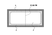
この場合、低融点金属封止膜4として塑性変形性が特に大きいSn―Bi-Cu系合金等を選択すれば、図5に示すような折りたたみ式のフレキシブル有機EL表示装置における繰り返し折り曲げに対しても、同図に破線で示す折り曲げ部における低融点金属封止膜4へのクラック又はひび割れの発生をより一層抑制することができる。なお、図5においては、封止膜層5及び水分吸収膜12は、図示省略されている。また、有機EL表示層2が表示部に相当する。
一方、折りたたみ式のフレキシブル有機EL表示装置における繰り返し折り曲げにより、例え低融点金属封止膜4にクラックやひび割れが発生したとしても、低融点金属封止膜4に対応させて封止膜層5に設けたフィルムヒータ6を加熱して低融点金属封止膜4を溶融又はアニールすることにより上記クラック又はひび割れを修復することができる。
この場合、使用開始から一定時間経過後又は折り曲げ回数が所定回数に達する毎に上記修復の動作を自動で行うようにすれば、フレキシブル有機EL表示装置の信頼性をより一層向上することができる。
図6は本発明によるフレキシブル表示装置(有機EL表示装置)の第2の実施形態を断面で示す要部拡大正面図である。
この第2の実施形態と上記第1の実施形態との相違点は、フィルムヒータ6が低融点金属封止膜4に対応させてフレキシブル基板1上に設けられている点である。
この第2の実施形態と上記第1の実施形態との相違点は、フィルムヒータ6が低融点金属封止膜4に対応させてフレキシブル基板1上に設けられている点である。
詳細には、例えばポリイミドとポリエチレンテレフタレートとの積層構造、又はポリエチレンテレフタレート等のフレキシブル基板1上にて、周辺回路部3及び低融点金属封止膜4に対応した領域に、ニッケル合金等の発熱抵抗体10をポリイミドシート等の絶縁材11で挟み込んだフィルムヒータ6が予め形成されている。
この第2の実施形態の封止方法は、第1の実施形態と同様に、上記フレキシブル基板1上にて有機EL表示層2の周辺領域に、該有機EL表示層2を駆動するために設けられた周辺回路部3の周縁部に沿って低融点金属封止膜4を形成する第1ステップと、有機EL表示層2、周辺回路部3及び低融点金属封止膜4を覆って封止膜層5を配置する第2ステップと、低融点金属封止膜4を加熱溶融させてフレキシブル基板1側と封止膜層5とを接合する第3ステップと、を実施するものである。
詳細には、低融点金属封止膜4をフレキシブル基板1側及び封止膜層5側から挟んで、低融点金属封止膜4との親和性の高い例えばNiやCu等の金属膜9が配置されているのが望ましい。
この場合、上記第3ステップは、封止膜層5側からレーザ光を照射し、又は上記フィルムヒータ6を加熱することにより低融点金属封止膜4を加熱溶融させて行われる。また、使用開始から一定時間経過後又は折り曲げ回数が所定回数に達する毎に上記フィルムヒータ6を加熱して低融点金属封止膜4を溶融又はアニールすることにより、例えば低融点金属封止膜4のクラック又はひび割れを修復する動作が自動実施される。
図7は本発明によるフレキシブル表示装置(有機EL表示装置)の第3の実施形態を断面で示す要部拡大正面図である。
この第3の実施形態と上記第1及び第2の実施形態との相違点は、低融点金属封止膜4を挟んで上下に設けられた金属膜9がフィルムヒータ6の機能を有している点である。
この第3の実施形態と上記第1及び第2の実施形態との相違点は、低融点金属封止膜4を挟んで上下に設けられた金属膜9がフィルムヒータ6の機能を有している点である。
この第3の実施形態の封止方法は、第1及び第2の実施形態と同様に、上記フレキシブル基板1上にて有機EL表示層2の周辺領域に、該有機EL表示層2を駆動するために設けられた周辺回路部3の周縁部に沿って低融点金属封止膜4を形成する第1ステップと、有機EL表示層2、周辺回路部3及び低融点金属封止膜4を覆って封止膜層5を配置する第2ステップと、低融点金属封止膜4を加熱溶融させてフレキシブル基板1側と封止膜層5とを接合する第3ステップと、を実施するものである。
詳細には、例えばポリイミドとポリエチレンテレフタレートとの積層構造等のフレキシブル基板1の有機EL表示層2形成面側、及び封止膜層5の有機EL表示層2側の面にて、低融点金属封止膜4に対応した領域に成膜又はめっきにより低融点金属封止膜4との親和性の高い、例えばNi等の発熱抵抗体の金属膜9(フィルムヒータ6)が予め形成されている。
この場合、上記第3ステップは、封止膜層5側からレーザ光を照射し、又は上記金属膜9(フィルムヒータ6)を加熱することにより低融点金属封止膜4を加熱溶融させて行われる。また、使用開始から一定時間経過後又は折り曲げ回数が所定回数に達する毎に上記金属膜9(フィルムヒータ6)を加熱して低融点金属封止膜4を溶融又はアニールすることにより、例えば低融点金属封止膜4のクラック又はひび割れを修復する動作が自動実施される。
図8は本発明によるフレキシブル表示装置の第4の実施形態を断面で示す要部拡大正面図である。
この第4の実施形態は、フレキシブル基板1上に液晶表示層13と封止膜層5とを積層したフレキシブル液晶表示装置であって、フレキシブル基板1上にて液晶表示層13の周辺領域に液晶表示層13を駆動するために設けられた周辺回路部3と、該周辺回路部3の周縁部に沿って設けられ、フレキシブル基板1と封止膜層5とを接合する低融点金属封止膜4と、低融点金属封止膜4に対応して設けられたフィルムヒータ6と、を備えたものである。
この第4の実施形態は、フレキシブル基板1上に液晶表示層13と封止膜層5とを積層したフレキシブル液晶表示装置であって、フレキシブル基板1上にて液晶表示層13の周辺領域に液晶表示層13を駆動するために設けられた周辺回路部3と、該周辺回路部3の周縁部に沿って設けられ、フレキシブル基板1と封止膜層5とを接合する低融点金属封止膜4と、低融点金属封止膜4に対応して設けられたフィルムヒータ6と、を備えたものである。
この第4の実施形態と上記第1~第3の実施形態との相違点は、表示層が液晶表示層13である点で、その他に関しては、上記第1~第3の実施形態と同様の技術的思想の適用が可能である。
一般に、液晶表示装置の封止においては、機械強度を増すためにカーボンファイバー等の材料を含む封止剤が使用される。しかしながら、このような封止剤は、塑性変形性を有しないためフレキシブル表示装置に適用するのが困難であった。
一方、本発明によるフレキシブル表示装置の封止方法は、封止剤として塑性変形性を有する低融点金属封止膜4を使用しているため、前述したようにフレキシブル表示装置に有効である。したがって、フレキシブル液晶表示装置の実現を可能にすることができる。
なお、以上の説明においては、基板がフレキシブル基板1の場合について説明したが、本発明はこれに限られず、基板は、ガラス等の硬質材料であってもよい。
1…フレキシブル基板(基板)
2…有機EL表示層(表示層)
3…周辺回路部
4…低融点金属封止膜
5…封止膜層
5′…別の封止膜層
6…フィルムヒータ
9…金属膜
13…液晶表示層(表示層)
2…有機EL表示層(表示層)
3…周辺回路部
4…低融点金属封止膜
5…封止膜層
5′…別の封止膜層
6…フィルムヒータ
9…金属膜
13…液晶表示層(表示層)
Claims (19)
- 可撓性の基板上に表示層と封止膜層とを積層したフレキシブル表示装置であって、
前記基板上にて前記表示層の周辺領域に前記表示層を駆動するために設けられた周辺回路部と、
前記周辺回路部の周縁部に沿って設けられ、前記基板と前記封止膜層とを接合する低融点金属封止膜と、
前記低融点金属封止膜に対応して設けられたフィルムヒータと、
を備えたことを特徴とするフレキシブル表示装置。 - 前記フィルムヒータは、前記低融点金属封止膜に対応させて前記封止膜層上に設けられることを特徴とする請求項1記載のフレキシブル表示装置。
- 前記フィルムヒータは、前記低融点金属封止膜に対応させて前記基板上に設けられることを特徴とする請求項1記載のフレキシブル表示装置。
- 前記フィルムヒータは、前記低融点金属封止膜との親和性の高い金属膜であり、前記低融点金属封止膜を前記基板側及び前記封止膜層側から挟んで設けられていることを特徴とする請求項1記載のフレキシブル表示装置。
- 前記低融点金属封止膜を前記基板側及び前記封止膜層側から挟んで、前記低融点金属封止膜との親和性の高い金属膜が配置されていることを特徴とする請求項1~3のいずれか1項に記載のフレキシブル表示装置。
- 前記基板と前記表示層との間には、さらに別の封止膜層が設けられていることを特徴とする請求項1~4のいずれか1項に記載のフレキシブル表示装置。
- 前記基板は、水分や酸素に対するバリア性を有するフレキシブル基板であることを特徴とする請求項1~4のいずれか1項に記載のフレキシブル表示装置。
- 前記基板は、水分や酸素に対して非バリア性のフレキシブル基板であることを特徴とする請求項6記載のフレキシブル表示装置。
- 前記低融点金属封止膜の融点は、前記表示層の耐熱温度よりも低いことを特徴とする請求項1~4のいずれか1項に記載のフレキシブル表示装置。
- 前記表示層は、有機EL表示層であることを特徴とする請求項1~4のいずれか1項に記載のフレキシブル表示装置。
- 前記表示層は、液晶表示層であることを特徴とする請求項1~4のいずれか1項に記載のフレキシブル表示装置。
- 可撓性の基板上に表示層と封止膜層とを積層したフレキシブル表示装置の封止方法であって、
前記基板上にて前記表示層の周辺領域に、該表示層を駆動するために設けられた周辺回路部の周縁部に沿って低融点金属封止膜を形成する第1ステップと、
前記表示層、前記周辺回路部及び前記低融点金属封止膜を覆って前記封止膜層を配置する第2ステップと、
前記低融点金属封止膜を加熱溶融させて前記基板と前記封止膜層とを接合する第3ステップと、
を実行することを特徴とするフレキシブル表示装置の封止方法。 - 前記第3ステップを実行した後、前記封止膜層の前記低融点金属封止膜との接合面とは反対側の面に、前記低融点金属封止膜に対応させてフィルムヒータを設ける第4ステップが実行されることを特徴とする請求項12記載のフレキシブル表示装置の封止方法。
- 前記封止膜層の前記低融点金属封止膜との接合面とは反対側の面、又は前記基板の前記表示層の形成面には、前記低融点金属封止膜に対応させて、予めフィルムヒータが設けられていることを特徴とする請求項12記載のフレキシブル表示装置の封止方法。
- 前記低融点金属封止膜を前記基板側及び前記封止膜層側から挟んで、前記低融点金属封止膜との親和性の高い発熱抵抗体の金属膜が配置されていることを特徴とする請求項12記載のフレキシブル表示装置の封止方法。
- 前記第3ステップは、前記フィルムヒータを加熱させて実行されることを特徴とする請求項14又は15記載のフレキシブル表示装置の封止方法。
- 前記低融点金属封止膜の融点は、前記表示層の耐熱温度よりも低いことを特徴とする請求項12~15のいずれか1項に記載のフレキシブル表示装置の封止方法。
- 前記表示層は、有機EL表示層であることを特徴とする請求項12~15のいずれか1項に記載のフレキシブル表示装置の封止方法。
- 前記表示層は、液晶表示層であることを特徴とする請求項12~15のいずれか1項に記載のフレキシブル表示装置の封止方法。
Applications Claiming Priority (2)
| Application Number | Priority Date | Filing Date | Title |
|---|---|---|---|
| JP2016-229228 | 2016-11-25 | ||
| JP2016229228A JP2018084764A (ja) | 2016-11-25 | 2016-11-25 | フレキシブル表示装置及びフレキシブル表示装置の封止方法 |
Publications (1)
| Publication Number | Publication Date |
|---|---|
| WO2018096995A1 true WO2018096995A1 (ja) | 2018-05-31 |
Family
ID=62195905
Family Applications (1)
| Application Number | Title | Priority Date | Filing Date |
|---|---|---|---|
| PCT/JP2017/041047 Ceased WO2018096995A1 (ja) | 2016-11-25 | 2017-11-15 | フレキシブル表示装置及びフレキシブル表示装置の封止方法 |
Country Status (3)
| Country | Link |
|---|---|
| JP (1) | JP2018084764A (ja) |
| TW (1) | TW201834232A (ja) |
| WO (1) | WO2018096995A1 (ja) |
Cited By (1)
| Publication number | Priority date | Publication date | Assignee | Title |
|---|---|---|---|---|
| CN113039594A (zh) * | 2018-11-06 | 2021-06-25 | 三星显示有限公司 | 显示装置 |
Families Citing this family (1)
| Publication number | Priority date | Publication date | Assignee | Title |
|---|---|---|---|---|
| KR102851564B1 (ko) | 2019-12-10 | 2025-08-28 | 엘지디스플레이 주식회사 | 표시장치 |
Citations (5)
| Publication number | Priority date | Publication date | Assignee | Title |
|---|---|---|---|---|
| JP2008298162A (ja) * | 2007-05-31 | 2008-12-11 | Canon Inc | マイクロ加工ワンショットバルブ、およびその製造方法 |
| JP2011137918A (ja) * | 2009-12-28 | 2011-07-14 | Fujifilm Corp | 金属封止電子素子の製造方法 |
| JP2012519938A (ja) * | 2009-03-04 | 2012-08-30 | グローバル・オーエルイーディー・テクノロジー・リミテッド・ライアビリティ・カンパニー | 活性有機材料を含む電子デバイスのための気密シール |
| US20160029502A1 (en) * | 2014-07-25 | 2016-01-28 | Samsung Display Co., Ltd. | Display module, display device, and method of manufacturing the same |
| US20160126487A1 (en) * | 2014-10-31 | 2016-05-05 | Samsung Display Co., Ltd. | Display device |
-
2016
- 2016-11-25 JP JP2016229228A patent/JP2018084764A/ja active Pending
-
2017
- 2017-11-15 WO PCT/JP2017/041047 patent/WO2018096995A1/ja not_active Ceased
- 2017-11-23 TW TW106140678A patent/TW201834232A/zh unknown
Patent Citations (5)
| Publication number | Priority date | Publication date | Assignee | Title |
|---|---|---|---|---|
| JP2008298162A (ja) * | 2007-05-31 | 2008-12-11 | Canon Inc | マイクロ加工ワンショットバルブ、およびその製造方法 |
| JP2012519938A (ja) * | 2009-03-04 | 2012-08-30 | グローバル・オーエルイーディー・テクノロジー・リミテッド・ライアビリティ・カンパニー | 活性有機材料を含む電子デバイスのための気密シール |
| JP2011137918A (ja) * | 2009-12-28 | 2011-07-14 | Fujifilm Corp | 金属封止電子素子の製造方法 |
| US20160029502A1 (en) * | 2014-07-25 | 2016-01-28 | Samsung Display Co., Ltd. | Display module, display device, and method of manufacturing the same |
| US20160126487A1 (en) * | 2014-10-31 | 2016-05-05 | Samsung Display Co., Ltd. | Display device |
Cited By (1)
| Publication number | Priority date | Publication date | Assignee | Title |
|---|---|---|---|---|
| CN113039594A (zh) * | 2018-11-06 | 2021-06-25 | 三星显示有限公司 | 显示装置 |
Also Published As
| Publication number | Publication date |
|---|---|
| JP2018084764A (ja) | 2018-05-31 |
| TW201834232A (zh) | 2018-09-16 |
Similar Documents
| Publication | Publication Date | Title |
|---|---|---|
| JP5080838B2 (ja) | 電子デバイスおよびその製造方法 | |
| JP4368908B2 (ja) | 有機電界発光表示装置の製造方法 | |
| JP4624309B2 (ja) | 有機電界発光表示装置及びその製造方法 | |
| TWI342078B (en) | Organic light emitting display of mother substrate unit and method of fabricating the same | |
| KR20090128430A (ko) | 유기 el 패널 및 그 제조 방법 | |
| JP2008170926A (ja) | 平板表示装置の製造方法 | |
| JP2007200845A (ja) | 有機電界発光表示装置 | |
| JP2009266922A (ja) | 有機発光装置 | |
| TW201521196A (zh) | 顯示裝置之製造方法及系統 | |
| JP2011070797A (ja) | 封止体の製造方法および有機el装置 | |
| JP2008288376A (ja) | 表示装置および表示装置の製造方法 | |
| JP2012230894A5 (ja) | ||
| JP2018084764A (ja) | フレキシブル表示装置及びフレキシブル表示装置の封止方法 | |
| TWI551914B (zh) | 用於撓性固態裝置之低溫接觸結構 | |
| JP5033505B2 (ja) | 表示パネル | |
| JP2011107432A (ja) | 電気光学装置の製造方法 | |
| JPWO2019167131A1 (ja) | フレキシブルoledデバイスの製造方法及び支持基板 | |
| JP4708360B2 (ja) | 有機エレクトロルミネセンス表示装置及びその製造方法 | |
| US20160126487A1 (en) | Display device | |
| WO2019130649A1 (ja) | 表示装置及びその製造方法 | |
| CN107507925A (zh) | 有机发光显示面板及制备方法、有机发光显示装置 | |
| WO2011096188A1 (ja) | 電子デバイスの製造方法 | |
| JP5127657B2 (ja) | 有機el表示装置の製造方法 | |
| JP2012190607A (ja) | 気密容器の製造方法 | |
| WO2015151659A1 (ja) | フレキシブル有機el表示装置の製造方法 |
Legal Events
| Date | Code | Title | Description |
|---|---|---|---|
| 121 | Ep: the epo has been informed by wipo that ep was designated in this application |
Ref document number: 17873043 Country of ref document: EP Kind code of ref document: A1 |
|
| NENP | Non-entry into the national phase |
Ref country code: DE |
|
| 122 | Ep: pct application non-entry in european phase |
Ref document number: 17873043 Country of ref document: EP Kind code of ref document: A1 |