WO2018096722A1 - 半導体装置 - Google Patents
半導体装置 Download PDFInfo
- Publication number
- WO2018096722A1 WO2018096722A1 PCT/JP2017/024054 JP2017024054W WO2018096722A1 WO 2018096722 A1 WO2018096722 A1 WO 2018096722A1 JP 2017024054 W JP2017024054 W JP 2017024054W WO 2018096722 A1 WO2018096722 A1 WO 2018096722A1
- Authority
- WO
- WIPO (PCT)
- Prior art keywords
- region
- silicon carbide
- inclined surface
- contact region
- semiconductor device
- Prior art date
- Legal status (The legal status is an assumption and is not a legal conclusion. Google has not performed a legal analysis and makes no representation as to the accuracy of the status listed.)
- Ceased
Links
Images





Classifications
-
- H—ELECTRICITY
- H10—SEMICONDUCTOR DEVICES; ELECTRIC SOLID-STATE DEVICES NOT OTHERWISE PROVIDED FOR
- H10D—INORGANIC ELECTRIC SEMICONDUCTOR DEVICES
- H10D62/00—Semiconductor bodies, or regions thereof, of devices having potential barriers
- H10D62/10—Shapes, relative sizes or dispositions of the regions of the semiconductor bodies; Shapes of the semiconductor bodies
- H10D62/124—Shapes, relative sizes or dispositions of the regions of semiconductor bodies or of junctions between the regions
- H10D62/126—Top-view geometrical layouts of the regions or the junctions
- H10D62/127—Top-view geometrical layouts of the regions or the junctions of cellular field-effect devices, e.g. multicellular DMOS transistors or IGBTs
-
- H—ELECTRICITY
- H10—SEMICONDUCTOR DEVICES; ELECTRIC SOLID-STATE DEVICES NOT OTHERWISE PROVIDED FOR
- H10D—INORGANIC ELECTRIC SEMICONDUCTOR DEVICES
- H10D12/00—Bipolar devices controlled by the field effect, e.g. insulated-gate bipolar transistors [IGBT]
- H10D12/01—Manufacture or treatment
- H10D12/031—Manufacture or treatment of IGBTs
-
- H—ELECTRICITY
- H10—SEMICONDUCTOR DEVICES; ELECTRIC SOLID-STATE DEVICES NOT OTHERWISE PROVIDED FOR
- H10D—INORGANIC ELECTRIC SEMICONDUCTOR DEVICES
- H10D30/00—Field-effect transistors [FET]
- H10D30/01—Manufacture or treatment
- H10D30/021—Manufacture or treatment of FETs having insulated gates [IGFET]
- H10D30/028—Manufacture or treatment of FETs having insulated gates [IGFET] of double-diffused metal oxide semiconductor [DMOS] FETs
- H10D30/0291—Manufacture or treatment of FETs having insulated gates [IGFET] of double-diffused metal oxide semiconductor [DMOS] FETs of vertical DMOS [VDMOS] FETs
- H10D30/0295—Manufacture or treatment of FETs having insulated gates [IGFET] of double-diffused metal oxide semiconductor [DMOS] FETs of vertical DMOS [VDMOS] FETs using recessing of the source electrodes
-
- H—ELECTRICITY
- H10—SEMICONDUCTOR DEVICES; ELECTRIC SOLID-STATE DEVICES NOT OTHERWISE PROVIDED FOR
- H10D—INORGANIC ELECTRIC SEMICONDUCTOR DEVICES
- H10D30/00—Field-effect transistors [FET]
- H10D30/01—Manufacture or treatment
- H10D30/021—Manufacture or treatment of FETs having insulated gates [IGFET]
- H10D30/028—Manufacture or treatment of FETs having insulated gates [IGFET] of double-diffused metal oxide semiconductor [DMOS] FETs
- H10D30/0291—Manufacture or treatment of FETs having insulated gates [IGFET] of double-diffused metal oxide semiconductor [DMOS] FETs of vertical DMOS [VDMOS] FETs
- H10D30/0297—Manufacture or treatment of FETs having insulated gates [IGFET] of double-diffused metal oxide semiconductor [DMOS] FETs of vertical DMOS [VDMOS] FETs using recessing of the gate electrodes, e.g. to form trench gate electrodes
-
- H—ELECTRICITY
- H10—SEMICONDUCTOR DEVICES; ELECTRIC SOLID-STATE DEVICES NOT OTHERWISE PROVIDED FOR
- H10D—INORGANIC ELECTRIC SEMICONDUCTOR DEVICES
- H10D30/00—Field-effect transistors [FET]
- H10D30/60—Insulated-gate field-effect transistors [IGFET]
-
- H—ELECTRICITY
- H10—SEMICONDUCTOR DEVICES; ELECTRIC SOLID-STATE DEVICES NOT OTHERWISE PROVIDED FOR
- H10D—INORGANIC ELECTRIC SEMICONDUCTOR DEVICES
- H10D30/00—Field-effect transistors [FET]
- H10D30/60—Insulated-gate field-effect transistors [IGFET]
- H10D30/64—Double-diffused metal-oxide semiconductor [DMOS] FETs
- H10D30/66—Vertical DMOS [VDMOS] FETs
-
- H—ELECTRICITY
- H10—SEMICONDUCTOR DEVICES; ELECTRIC SOLID-STATE DEVICES NOT OTHERWISE PROVIDED FOR
- H10D—INORGANIC ELECTRIC SEMICONDUCTOR DEVICES
- H10D62/00—Semiconductor bodies, or regions thereof, of devices having potential barriers
- H10D62/10—Shapes, relative sizes or dispositions of the regions of the semiconductor bodies; Shapes of the semiconductor bodies
- H10D62/117—Shapes of semiconductor bodies
-
- H—ELECTRICITY
- H10—SEMICONDUCTOR DEVICES; ELECTRIC SOLID-STATE DEVICES NOT OTHERWISE PROVIDED FOR
- H10D—INORGANIC ELECTRIC SEMICONDUCTOR DEVICES
- H10D62/00—Semiconductor bodies, or regions thereof, of devices having potential barriers
- H10D62/10—Shapes, relative sizes or dispositions of the regions of the semiconductor bodies; Shapes of the semiconductor bodies
- H10D62/13—Semiconductor regions connected to electrodes carrying current to be rectified, amplified or switched, e.g. source or drain regions
- H10D62/149—Source or drain regions of field-effect devices
- H10D62/151—Source or drain regions of field-effect devices of IGFETs
- H10D62/156—Drain regions of DMOS transistors
- H10D62/157—Impurity concentrations or distributions
-
- H—ELECTRICITY
- H10—SEMICONDUCTOR DEVICES; ELECTRIC SOLID-STATE DEVICES NOT OTHERWISE PROVIDED FOR
- H10D—INORGANIC ELECTRIC SEMICONDUCTOR DEVICES
- H10D62/00—Semiconductor bodies, or regions thereof, of devices having potential barriers
- H10D62/10—Shapes, relative sizes or dispositions of the regions of the semiconductor bodies; Shapes of the semiconductor bodies
- H10D62/17—Semiconductor regions connected to electrodes not carrying current to be rectified, amplified or switched, e.g. channel regions
- H10D62/213—Channel regions of field-effect devices
- H10D62/221—Channel regions of field-effect devices of FETs
- H10D62/235—Channel regions of field-effect devices of FETs of IGFETs
- H10D62/292—Non-planar channels of IGFETs
-
- H—ELECTRICITY
- H10—SEMICONDUCTOR DEVICES; ELECTRIC SOLID-STATE DEVICES NOT OTHERWISE PROVIDED FOR
- H10D—INORGANIC ELECTRIC SEMICONDUCTOR DEVICES
- H10D62/00—Semiconductor bodies, or regions thereof, of devices having potential barriers
- H10D62/40—Crystalline structures
- H10D62/405—Orientations of crystalline planes
-
- H—ELECTRICITY
- H10—SEMICONDUCTOR DEVICES; ELECTRIC SOLID-STATE DEVICES NOT OTHERWISE PROVIDED FOR
- H10D—INORGANIC ELECTRIC SEMICONDUCTOR DEVICES
- H10D62/00—Semiconductor bodies, or regions thereof, of devices having potential barriers
- H10D62/80—Semiconductor bodies, or regions thereof, of devices having potential barriers characterised by the materials
- H10D62/83—Semiconductor bodies, or regions thereof, of devices having potential barriers characterised by the materials being Group IV materials, e.g. B-doped Si or undoped Ge
- H10D62/832—Semiconductor bodies, or regions thereof, of devices having potential barriers characterised by the materials being Group IV materials, e.g. B-doped Si or undoped Ge being Group IV materials comprising two or more elements, e.g. SiGe
- H10D62/8325—Silicon carbide
-
- H—ELECTRICITY
- H10—SEMICONDUCTOR DEVICES; ELECTRIC SOLID-STATE DEVICES NOT OTHERWISE PROVIDED FOR
- H10D—INORGANIC ELECTRIC SEMICONDUCTOR DEVICES
- H10D64/00—Electrodes of devices having potential barriers
- H10D64/01—Manufacture or treatment
- H10D64/011—Manufacture or treatment of electrodes ohmically coupled to a semiconductor
-
- H—ELECTRICITY
- H10—SEMICONDUCTOR DEVICES; ELECTRIC SOLID-STATE DEVICES NOT OTHERWISE PROVIDED FOR
- H10D—INORGANIC ELECTRIC SEMICONDUCTOR DEVICES
- H10D64/00—Electrodes of devices having potential barriers
- H10D64/01—Manufacture or treatment
- H10D64/013—Manufacture or treatment of electrodes having a conductor capacitively coupled to a semiconductor by an insulator
- H10D64/01366—Manufacture or treatment of electrodes having a conductor capacitively coupled to a semiconductor by an insulator the semiconductor being silicon carbide
-
- H—ELECTRICITY
- H10—SEMICONDUCTOR DEVICES; ELECTRIC SOLID-STATE DEVICES NOT OTHERWISE PROVIDED FOR
- H10D—INORGANIC ELECTRIC SEMICONDUCTOR DEVICES
- H10D64/00—Electrodes of devices having potential barriers
- H10D64/20—Electrodes characterised by their shapes, relative sizes or dispositions
-
- H—ELECTRICITY
- H10—SEMICONDUCTOR DEVICES; ELECTRIC SOLID-STATE DEVICES NOT OTHERWISE PROVIDED FOR
- H10D—INORGANIC ELECTRIC SEMICONDUCTOR DEVICES
- H10D64/00—Electrodes of devices having potential barriers
- H10D64/20—Electrodes characterised by their shapes, relative sizes or dispositions
- H10D64/23—Electrodes carrying the current to be rectified, amplified, oscillated or switched, e.g. sources, drains, anodes or cathodes
- H10D64/251—Source or drain electrodes for field-effect devices
- H10D64/252—Source or drain electrodes for field-effect devices for vertical or pseudo-vertical devices
- H10D64/2527—Source or drain electrodes for field-effect devices for vertical or pseudo-vertical devices for vertical devices wherein the source or drain electrodes are recessed in semiconductor bodies
-
- H—ELECTRICITY
- H10—SEMICONDUCTOR DEVICES; ELECTRIC SOLID-STATE DEVICES NOT OTHERWISE PROVIDED FOR
- H10D—INORGANIC ELECTRIC SEMICONDUCTOR DEVICES
- H10D64/00—Electrodes of devices having potential barriers
- H10D64/60—Electrodes characterised by their materials
- H10D64/66—Electrodes having a conductor capacitively coupled to a semiconductor by an insulator, e.g. MIS electrodes
-
- H—ELECTRICITY
- H10—SEMICONDUCTOR DEVICES; ELECTRIC SOLID-STATE DEVICES NOT OTHERWISE PROVIDED FOR
- H10D—INORGANIC ELECTRIC SEMICONDUCTOR DEVICES
- H10D62/00—Semiconductor bodies, or regions thereof, of devices having potential barriers
- H10D62/10—Shapes, relative sizes or dispositions of the regions of the semiconductor bodies; Shapes of the semiconductor bodies
- H10D62/17—Semiconductor regions connected to electrodes not carrying current to be rectified, amplified or switched, e.g. channel regions
- H10D62/393—Body regions of DMOS transistors or IGBTs
Definitions
- the present disclosure relates to a semiconductor device.
- MOSFET metal-oxide-semiconductor-field-effect-transistor
- a single crystal silicon carbide substrate a silicon carbide epitaxial layer formed on one main surface of the single crystal silicon carbide substrate, and recesses and protrusions formed on the surface of the silicon carbide epitaxial layer. And an inclined surface formed between the concave portion and the convex portion.
- a first contact region of the first conductivity type formed on the inclined surface side of the bottom surface of the recess; a second contact region of the second conductivity type in contact with the first contact region on the bottom surface of the recess; It has a first conductivity type drift region formed on the upper surface of the convex portion and a second conductivity type body region formed on an inclined surface between the first contact region and the drift region.
- the angle of the inclined surface with respect to one main surface of the single crystal silicon carbide substrate is not less than 40 ° and not more than 70 °.
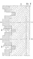
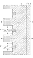
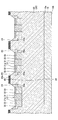
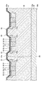
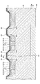
- FIG. 1 is a plan view schematically illustrating a semiconductor layer of a semiconductor device according to one embodiment of the present disclosure.
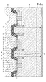
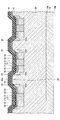
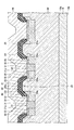
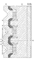
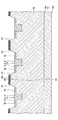
- FIG. 2 is a cross-sectional view schematically illustrating a semiconductor device according to one embodiment of the present disclosure.
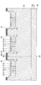
- FIG. 3 is a process diagram (1) of a method for manufacturing a semiconductor device according to an aspect of the present disclosure.
- FIG. 4 is a process diagram (2) of the method for manufacturing the semiconductor device according to an aspect of the present disclosure.
- FIG. 5 is a process diagram (3) of the method for manufacturing a semiconductor device according to one embodiment of the present disclosure.
- FIG. 6 is a process diagram (4) of the method for manufacturing a semiconductor device according to one embodiment of the present disclosure.
- FIG. 1 is a plan view schematically illustrating a semiconductor layer of a semiconductor device according to one embodiment of the present disclosure.
- FIG. 2 is a cross-sectional view schematically illustrating a semiconductor device according to one embodiment of the present disclosure.
- FIG. 3 is a process diagram (1) of a method
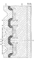
- FIG. 7 is a process diagram (5) of the method for manufacturing a semiconductor device according to an aspect of the present disclosure.
- FIG. 8 is a process diagram (6) of the method for manufacturing a semiconductor device according to one embodiment of the present disclosure.
- FIG. 9 is a process diagram (7) of the method for manufacturing a semiconductor device according to an aspect of the present disclosure.
- FIG. 10 is a process diagram (8) of the method for manufacturing the semiconductor device according to one embodiment of the present disclosure.
- FIG. 11 is a process diagram (9) of the method for manufacturing a semiconductor device according to one embodiment of the present disclosure.
- FIG. 12 is a process diagram (10) of the method for manufacturing the semiconductor device according to one embodiment of the present disclosure.
- FIG. 13 is a process diagram (11) of the method for manufacturing a semiconductor device according to an aspect of the present disclosure.
- FIG. 14 is a process diagram (12) of the method for manufacturing the semiconductor device according to one embodiment of the present disclosure.
- FIG. 15 is a process diagram (13) of the method for manufacturing the semiconductor device according to one embodiment of the present disclosure.
- FIG. 16 is a process diagram (14) of the method for manufacturing a semiconductor device according to one embodiment of the present disclosure.
- FIG. 17 is an explanatory diagram (1) of the manufacturing method of the first modification of the semiconductor device according to one embodiment of the present disclosure.
- FIG. 18 is an explanatory diagram (2) of the manufacturing method of Modification 1 of the semiconductor device according to one embodiment of the present disclosure.
- FIG. 19 is an explanatory diagram (3) of the manufacturing method of Modification 1 of the semiconductor device according to one embodiment of the present disclosure.
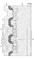
- FIG. 20 is a cross-sectional view schematically illustrating Modification 1 of the semiconductor device according to one aspect of the present disclosure.
- FIG. 21 is a cross-sectional view schematically illustrating Modification Example 2 of the semiconductor device according to one aspect of the present disclosure.
- Silicon carbide has various crystal polytypes (polytypes), each having a different physical property value, but the 4H type is preferred for use in power devices.
- silicon carbide (4H—SiC) having a 4H type crystal structure is described without any special designation.
- a semiconductor device includes a single crystal silicon carbide substrate, a silicon carbide epitaxial layer formed on one main surface of the single crystal silicon carbide substrate, and a surface of the silicon carbide epitaxial layer.
- the angle of the inclined surface with respect to the main surface is 40 ° or more and 70 ° or less.
- the channel mobility in the in-plane direction of the silicon carbide on the ⁇ 0001 ⁇ plane is low, and the on-resistance is high. Since the silicon carbide single crystal has higher channel mobility in the ⁇ 03-3-8 ⁇ plane than in the ⁇ 0001 ⁇ plane, by forming a channel in the ⁇ 03-3-8 ⁇ plane, the on-resistance is reduced. Can be lowered.
- the inventor of the present application has researched that a concave portion and a convex portion, and an inclined surface between the concave portion and the convex portion are formed on the surface of the silicon carbide epitaxial layer. It was found that the electric field concentration is mitigated by flowing toward. Therefore, by using a structure in which the inclined surface is the ⁇ 03-3-8 ⁇ surface and electrons flow from the concave portion toward the convex portion, channel mobility can be increased, electric field concentration is reduced, and reliability is improved. Can be improved. Note that in a silicon carbide single crystal, the channel mobility is higher than that of the ⁇ 0001 ⁇ plane even in the ⁇ 01-1-2 ⁇ plane and the ⁇ 01-1-4 ⁇ plane other than the ⁇ 03-3-8 ⁇ plane. Therefore, the inclined surface may be formed by a ⁇ 01-1-2 ⁇ plane or a ⁇ 01-1-4 ⁇ plane.
- the boundary between the drift region and the body region is located on the inclined surface, and the boundary is perpendicular to one main surface of the single crystal silicon carbide substrate.
- the impurity concentration in the body region is 1 ⁇ 10 17 cm ⁇ 3 or more and 3 ⁇ 10 19 cm ⁇ 3 or less.
- a second conductivity type semiconductor region having an impurity concentration higher than that of the body region is the second contact. It is formed in contact with the region and the body region.
- the planar shape of the recess is a hexagon.
- the single crystal silicon carbide substrate has a 4H type crystal structure
- the silicon carbide epitaxial layer has a 4H type crystal structure
- a semiconductor device includes a single-crystal silicon carbide substrate having a 4H-type crystal structure, and one main surface of the single-crystal silicon carbide substrate having a 4H-type crystal structure.
- a silicon carbide epitaxial layer formed on the silicon carbide epitaxial layer, a concave portion and a convex portion formed on the surface of the silicon carbide epitaxial layer, an inclined surface formed between the concave portion and the convex portion, and the bottom surface of the concave portion.
- Gate insulating film and said gate insulating A gate electrode formed on the film, a source electrode formed on the first contact region and the second contact region, and a drain formed on the other main surface of the single crystal silicon carbide substrate
- An angle of the inclined surface with respect to one main surface of the single crystal silicon carbide substrate is not less than 40 ° and not more than 70 °, and a boundary between the drift region and the body region is the inclined surface
- the boundary is perpendicular to one main surface of the single crystal silicon carbide substrate, and the impurity concentration in the body region is 1 ⁇ 10 17 cm ⁇ 3 or more and 3 ⁇ 10 19 cm ⁇ . 3 or less.
- the present embodiment an embodiment of the present disclosure (hereinafter referred to as “the present embodiment”) will be described in detail, but the present embodiment is not limited thereto.
- FIG. 1 is a top view of a semiconductor portion of the semiconductor device according to the present embodiment
- FIG. 2 is a cross-sectional view of the semiconductor device cut at a portion corresponding to the alternate long and short dash line 1A-1B in FIG.
- description of the gate insulating film 41, the gate electrode 42, the interlayer insulating film 43, the source electrode 44, and the like shown in FIG. 2 is omitted.
- a plurality of recesses and protrusions are formed on the surface of the silicon carbide epitaxial layer formed on one main surface of the silicon carbide substrate, and an inclined surface is provided between the recesses and the protrusions.
- This is a vertical MOSFET having a structure.
- a silicon carbide epitaxial layer for forming n drift region 30 and the like is formed on one main surface 10a of n-type single crystal silicon carbide substrate 10, and this silicon carbide epitaxial layer A plurality of concave portions 21 and convex portions 22 are formed on the surface.
- the bottom surface of the concave portion 21 is formed in a hexagonal shape, and the convex portion 22 is formed so as to surround the periphery of the hexagonal concave portion 21.
- an inclined surface 23 is formed between the concave portion 21 and the convex portion 22, and this inclined surface 23 is a ⁇ 03-3-8 ⁇ surface having a high channel mobility.
- the semiconductor device has a structure in which the convex portions 22 are formed between the concave portions 21 and the concave portions 21 and the inclined surfaces 23 are formed on both sides of the convex portions 22.
- a region where a p + contact region 31 and an n + contact region 32 described later are formed is a recess 21, and a region where a p body region 33 is formed and a region where a part of an n drift region 30 is formed.
- the convex surface 22 is a region where the n drift region 30 outside the inclined surface 23 is formed.
- a solid line 22 b indicates the boundary between the inclined surface 23 and the convex portion 22.
- single crystal silicon carbide substrate 10 has a 4H type crystal structure, and the silicon carbide epitaxial layer formed on one main surface 10a of single crystal silicon carbide substrate 10 is also 4H type.
- the crystal structure is
- the angle of the ⁇ 03-3-8 ⁇ plane with respect to the ⁇ 0001 ⁇ plane is about 54.7 °.
- the ⁇ 01-1-2 ⁇ plane other than the ⁇ 03-3-8 ⁇ plane and the ⁇ 01-1-4 ⁇ plane move more than the ⁇ 0001 ⁇ plane. Since the degree is high, the inclined surface 23 may be formed by these surfaces.
- the angle of the ⁇ 01-1-2 ⁇ plane with respect to the ⁇ 0001 ⁇ plane is 62.1 °
- the angle of the ⁇ 01-1-4 ⁇ plane with respect to the ⁇ 0001 ⁇ plane is 43.3 °.
- the angle ⁇ of the inclined surface 23 with respect to the one main surface 10a and the like of the single crystal silicon carbide substrate 10 is preferably 40 ° or more and 70 ° or less.
- the angle ⁇ of the inclined surface 23 with respect to one main surface 10a and the like of the single crystal silicon carbide substrate 10 is less than 40 °, the inclined surface 23 becomes wider, the semiconductor device becomes larger, and when the angle exceeds 70 °, This is because it becomes difficult to form a p body region 33 described later by ion implantation.
- a p + contact region 31 is formed at the center of the bottom surface 21 a of the recess 21, and an n + contact region 32 is formed around the p + contact region 31 of the bottom surface 21 a of the recess 21.
- a p body region 33 is formed at a position deeper than the n + contact region 32. P body region 33 is in contact with the lower end of n + contact region 32.
- the n drift region 30 is formed at a position deeper than the p + contact region 31 and the p body region 33 on the bottom surface 21a of the concave portion 21, and the convex portion 22 is formed by the n drift region 30, and the inclined surface 23 Then, the p body region 33 and the n drift region 30 are in contact with each other.
- the impurity concentration of n-type single crystal silicon carbide substrate 10 is 1 ⁇ 10 19 cm ⁇ 3
- the impurity concentration of n drift region 30 is 1 ⁇ 10 15 to 2 ⁇ 10. 16 cm ⁇ 3
- the impurity concentration of the p + contact region 31 is 2 ⁇ 10 20 cm ⁇ 3
- the impurity concentration of the n + contact region 32 is 1 ⁇ 10 20 cm ⁇ 3
- the impurity concentration of the p body region 33 is not less than 1 ⁇ 10 17 cm ⁇ 3 and not more than 3 ⁇ 10 19 cm ⁇ 3 , for example, about 5 ⁇ 10 17 cm ⁇ 3 .
- the gate insulating film 41 is formed on the upper surface 22 a of the convex portion 22, the inclined surface 23, and the bottom surface 21 a of the concave portion 21 in the vicinity of the inclined surface 23.
- a gate electrode 42 is formed on 41. Therefore, the gate electrode 42 is formed on the upper surface 22 a of the convex portion 22, the inclined surface 23, and the bottom surface 21 a of the concave portion 21 in the vicinity of the inclined surface 23 via the gate insulating film 41.
- An interlayer insulating film 43 is formed on the gate electrode 42 and the gate insulating film 41, and the gate electrode 42 is covered with the interlayer insulating film 43. Furthermore, a source electrode 44 is formed on the bottom surface 21 a of the recess 21, and the source electrode 44 is in contact with the p + contact region 31 and the n + contact region 32 on the bottom surface 21 a of the recess 21. The source electrode 44 is also formed on the interlayer insulating film 43, and the bottom surfaces 21 a of the plurality of recesses 21 are connected by one source electrode 44.
- a drain electrode 45 is formed on the other main surface 10b of single crystal silicon carbide substrate 10.
- boundary 33 a between the p body region 33 and the n drift region 30 is located on the inclined surface 23. Further, in the vicinity of inclined surface 23, boundary 33a between p body region 33 and n drift region 30 is perpendicular to one main surface 10a of single crystal silicon carbide substrate 10 and the like.
- one main surface 10a and the other main surface 10b of single-crystal silicon carbide substrate 10 have an off angle of ⁇ 3 ° or more and 3 ° or more with respect to the ⁇ 0001 ⁇ plane (c-plane) of single-crystal silicon carbide substrate 10. Off-substrate is used.
- angle ⁇ of inclined surface 23 with respect to one main surface 10a of single-crystal silicon carbide substrate 10 is about 55 °. ⁇ 3 °. Therefore, the angle formed by the boundary 33a between the p body region 33 and the n drift region 30 and the inclined surface 23 is wider on the n drift region 30 side than on the p body region 33 side.
- a channel is formed on the inclined surface 23 of the p body region 33, and the n + contact region 32, the n drift region 30, Are electrically connected.
- electrons as carriers are in order of n + contact region 32, p body region 33, n drift region 30, single crystal silicon carbide substrate 10, and drain electrode 45 from source electrode 44 as indicated by the dashed arrow.
- Flowing. Therefore, in the p body region 33 where the channel is formed, electrons flow toward the upper surface 22a of the convex portion 22 along the inclined surface 23 where the channel is formed. It flows toward the formed single crystal silicon carbide substrate 10 side.
- the inclined surface 23 of the p body region 33 in which the channel is formed is a ⁇ 03-3-8 ⁇ surface having a high channel mobility, the on-resistance can be lowered. Further, since the position where the source electrode 44 is in contact with the n + contact region 32 is lower than the inclined surface 23 of the p body region 33 where the channel is formed, the electric field concentration in the gate insulating film 41 can be reduced. And the reliability of the semiconductor device can be improved.
- n-type single crystal silicon carbide substrate 10 is prepared.
- n-type conductivity type is formed on one main surface 10 a of single-crystal silicon carbide substrate 10.
- a silicon carbide epitaxial layer 20 is formed.
- Silicon carbide epitaxial layer 20 is formed to form n drift region 30, p + contact region 31, n + contact region 32, and p body region 33.
- p + contact region 31, n + contact region 32, and p body region 33 are formed by ion implantation into silicon carbide epitaxial layer 20, and regions that are not ion implanted in silicon carbide epitaxial layer 20 are formed.
- N drift region 30 is formed by ion implantation into silicon carbide epitaxial layer 20.
- Silicon carbide epitaxial layer 20 is formed by epitaxial growth by CVD (chemical vapor deposition). At this time, a mixed gas of silane (SiH 4 ) and propane (C 3 H 8 ) is used as the source gas, and hydrogen gas (H 2 ) is used as the carrier gas. For example, nitrogen (N), phosphorus (P), or the like is used as the impurity element whose conductivity type is n-type.
- the concentration of the impurity element doped in silicon carbide epitaxial layer 20 is preferably 5 ⁇ 10 15 cm ⁇ 3 or more and 5 ⁇ 10 16 cm ⁇ 3 or less. In this manner, silicon carbide epitaxial layer 20 serving as surface 20a is formed on one main surface 10a of single crystal silicon carbide substrate 10.
- N is used as an n-type impurity element
- the concentration of the impurity element in the n-type single crystal silicon carbide substrate 10 is 3 ⁇ 10 18 cm ⁇ 3 .
- a plurality of recesses 21 are formed in surface 20 a of silicon carbide epitaxial layer 20.
- a photoresist is applied to the surface 20a of the silicon carbide epitaxial layer 20, and exposure and development are performed by an exposure apparatus, thereby forming an etching mask 61 having an opening 61a in a region where the recess 21 is formed.
- silicon carbide epitaxial layer 20 in a region where etching mask 61 is not formed is partially removed from surface 20a by dry etching such as RIE to form a plurality of recesses 21.
- dry etching methods such as RIE include ICP (Inductive Coupled Plasma) -RIE and the like.
- SF 6 or a mixed gas of SF 6 and O 2 can be used as an etching gas.
- a plurality of concave portions 21 and convex portions 22 are formed, and the side walls of concave portions 21 are formed substantially perpendicular to one main surface 10a of single crystal silicon carbide substrate 10.
- the recess 21 formed in this way has a hexagonal shape when viewed from the top.
- a p + contact region 31 is formed by ion-implanting a p-type impurity element into the central portion of the bottom surface 21 a of the recess 21. Specifically, after removing the etching mask 61, an ion implantation mask 62 having an opening 62a in a region where the p + contact region 31 is formed is formed. Thereafter, p + contact region 31 is formed by ion-implanting a p-type impurity element into silicon carbide epitaxial layer 20 in the region where opening 62a is formed.
- the p-type impurity element examples include Al, and ion implantation is performed by adjusting the dose amount and the acceleration voltage so that the impurity concentration in the p + contact region 31 is a desired concentration up to a desired depth.
- the impurity concentration in the p + contact region 31 is 1 ⁇ 10 20 cm ⁇ 3 .
- an n + contact region 32 is formed by ion-implanting an n-type impurity element around the p + contact region 31 on the bottom surface 21 a of the recess 21. Specifically, after removing the ion implantation mask 62, an ion implantation mask 63 having an opening 63a on the bottom surface 21a of the recess 21 is formed. Thereafter, n + contact region 32 is formed by ion-implanting an n-type impurity element into silicon carbide epitaxial layer 20 in the region where opening 63a is formed. As the n-type impurity element, N, P, or the like is used.
- the n + contact region 32 is formed in a region shallower than the p + contact region 31. For this reason, an n-type impurity element is also implanted into a shallow region of the p + contact region 31, but the concentration of the impurity element implanted into the n + contact region 32 is the concentration of the impurity element in the p + contact region 31.
- the p-type is maintained because it is lower. Therefore, ion implantation is performed by adjusting the dose amount and the acceleration voltage so that the impurity concentration in the n + contact region 32 becomes a desired concentration up to a desired depth.
- the impurity concentration in the n + contact region 32 is 5 ⁇ 10 19 cm ⁇ 3 .
- a p-type impurity element is ion-implanted into a region deeper than the n + contact region 32 on the bottom surface 21 a of the concave portion 21 and a part of the convex portion 22 around the concave portion 21.
- the p body region 33 is formed.
- an ion implantation mask 64 having an opening 64a is formed in a region where the p body region 33 is formed.
- p body region 33 is formed by ion-implanting a p-type impurity element into silicon carbide epitaxial layer 20 in the region where opening 64a is formed.
- the p body region 33 is formed in a region deeper than the n + contact region 32 and a part of the convex portion 22 in the vicinity of the concave portion 21.
- ion implantation is performed by adjusting the dose amount and the acceleration voltage so that the impurity concentration in the p body region 33 becomes a desired concentration up to a desired depth.
- the impurity concentration in the p body region 33 is 2 ⁇ 10 17 cm ⁇ 3 .
- a p-type impurity element is also implanted into the n + contact region 32, but the concentration of the impurity element implanted into the p body region 33 is higher than the concentration of the impurity element in the n + contact region 32. Since it is low, n-type is maintained. Further, an impurity element which becomes p-type is implanted also into the p + contact region 31, but it remains p-type because it is the same p-type. In this way, by implanting the impurity element into the silicon carbide epitaxial layer 20, the p + contact region 31, the n + contact region 32, and the p body region 33 are formed.
- n drift region 30 the region where the impurity element is not ion-implanted becomes n drift region 30.
- n drift region 30 a region where no impurity element is ion-implanted.
- an inclined surface 23 serving as a ⁇ 03-3-8 ⁇ plane is formed between the concave portion 21 and the convex portion 22.
- a silicon oxide film is formed on the entire surface by CVD or the like, a photoresist is then applied on the formed silicon oxide film, and exposure by an exposure apparatus is performed.
- a resist pattern (not shown) is formed on the silicon oxide film in the region where the thermal etching mask 65 is to be formed.
- the silicon oxide film in the region where the resist pattern is not formed is removed by dry etching such as RIE, so that the bottom surface 21a and the side surface of the concave portion 21 and a part of the upper surface 22a of the convex portion 22 in the vicinity of the concave portion 21 are exposed. .
- a thermal etching mask 65 is formed from the remaining silicon oxide film. The thermal etching mask 65 is formed on the n drift region 30 on the upper surface 22a of the convex portion 22, and the n drift region 30 is partially exposed between the thermal etching mask 65 and the boundary 33a.
- thermal etching is performed using the thermal etching mask 65 as a mask.
- a mixed gas of oxygen gas and chlorine gas is used as a reaction gas, for example, at a temperature of 700 ° C. or higher and 1000 ° C. or lower.
- the n drift region 30, the p + contact region 31, the n + contact region 32, and the p body region 33 in a region where the thermal etching mask 65 is not formed have a predetermined crystal plane ⁇ 03-3 -8 ⁇ surface appears. In this way, a ⁇ 03-3-8 ⁇ surface that becomes the inclined surface 23 can be formed between the concave portion 21 and the convex portion 22 by thermal etching.
- reaction gas may contain a carrier gas in addition to the chlorine gas and the oxygen gas described above.
- the carrier gas for example, nitrogen (N 2 ) gas, argon gas, helium gas, or the like can be used.
- the etching rate of SiC is, for example, about 70 ⁇ m / hr.
- silicon oxide (SiO 2 ) is used as the thermal etching mask 65, the selection ratio of SiC with respect to SiO 2 is extremely large. Therefore, when etching SiC, the thermal etching mask 65 formed of SiO 2 is hardly used. It will not be etched.
- the crystal plane of the inclined surface 23 formed by thermal etching is a ⁇ 03-3-8 ⁇ plane. That is, in the etching under the conditions described above, the ⁇ 03-3-8 ⁇ plane, which is the crystal plane with the slowest etching rate, is self-formed as the inclined plane 23 between the concave portion 21 and the convex portion 22.
- a boundary 33 a perpendicular to one main surface 10 a of single-crystal silicon carbide substrate 10 between n drift region 30 and p body region 33 is formed on inclined surface 23.
- the inclined surface 23 may be formed by a ⁇ 01-1-2 ⁇ surface, a ⁇ 01-1-4 ⁇ surface, or the like other than the ⁇ 03-3-8 ⁇ surface.
- a gate insulating film 41 is formed on the bottom surface 21 a of the concave portion 21, the upper surface 22 a of the convex portion 22 and the surface of the inclined surface 23.
- the gate insulating film 41 is formed by thermally oxidizing the surface of silicon carbide forming the bottom surface 21a of the concave portion 21, the upper surface 22a of the convex portion 22, and the inclined surface 23.
- a conductor film 42a is formed on the gate insulating film 41, and the conductor film 42a is processed to form the gate electrode 42 as shown in FIG. To do.
- a conductor film 42a is formed on the gate insulating film 41 by forming a metal film or the like by sputtering, and then, on the conductor film 42a, A photoresist is applied, and exposure and development are performed by an exposure apparatus. Thereby, a resist pattern (not shown) is formed on the region of the conductor film 42a where the gate electrode 42 is formed. Thereafter, the conductor film 42a in the region where the resist pattern is not formed is removed by etching. As a result, as shown in FIG.
- the gate electrode 42 is formed on the upper surface 22 a of the convex portion 22 through the gate insulating film 41, the inclined surface 23, and the bottom surface 21 a of the concave portion 21 in the vicinity of the inclined surface 23. Thereafter, the resist pattern (not shown) is removed.
- an interlayer insulating film 43 is formed on the gate insulating film 41 and the gate electrode 42.
- an insulating silicon oxide film or the like can be used as the interlayer insulating film 43.
- a part of the gate insulating film 41 and the interlayer insulating film 43 is removed to form a contact hole 43a, and the p + contact region 31 and the n + contact on the bottom surface 21a of the recess 21 are formed.
- a part of the region 32 is exposed.
- a photoresist is applied on the interlayer insulating film 43, and exposure and development are performed by an exposure apparatus, thereby providing an opening in a region where the contact hole 43a is formed on the interlayer insulating film 43.
- a resist pattern (not shown) is formed.
- the contact hole 43a is formed by removing the gate insulating film 41 and the interlayer insulating film 43 in the region where the resist pattern is not formed by dry etching such as RIE by dry etching such as RIE. As described above, by forming the contact hole 43a, the p + contact region 31 and the n + contact region 32 are partially exposed on the bottom surface 21a of the recess 21.
- the source electrode 44 is formed on the interlayer insulating film 43, the p + contact region 31, and the n + contact region 32 with a conductor film, for example, a metal film.
- a conductor film for example, a metal film.
- a drain electrode 45 is formed on the other main surface 10b of the single crystal silicon carbide substrate 10 with a conductor film, for example, a metal film or the like. Thereby, the semiconductor device in this embodiment can be manufactured.
- thermal etching is performed after the step shown in FIG. 7, ion implantation for forming the p body region 33 is performed, and thermal etching is performed again. It may be a thing. Specifically, after the step shown in FIG. 7, the ion implantation mask 63 is removed, and as shown in FIG. 17, a thermal etching mask 65 is formed, and thermal etching is performed. Thereby, the inclined surface 23 is formed between the concave portion 21 and the convex portion 22.
- a p body region 33 is formed by ion implantation of a p-type impurity element into a region deeper than the n + contact region 32 of the bottom surface 21a of the recess 21 and the inclined surface 23. To do. Thereby, a boundary 33 a between n drift region 30 and p body region 33 between thermal etching mask 65 and inclined surface 23 is formed perpendicular to one main surface 10 a of single crystal silicon carbide substrate 10.
- thermal etching is performed again.
- a part of the semiconductor in inclined surface 23 is removed, and the boundary between n drift region 30 and p body region 33 is located on inclined surface 23.
- the inclined surface 23 which becomes the ⁇ 03-3-8 ⁇ plane can be formed between the concave portion 21 and the convex portion 22.
- the semiconductor device having the structure shown in FIG. 20 can be manufactured by performing the steps after the step shown in FIG.
- the boundary between the p body region 33 and the n drift region 30 is formed in an inclined shape, not a step shape, below the inclined surface 23, so that the electric field concentration can be further relaxed. Reliability can be improved.
- the semiconductor device according to the present embodiment may have a structure in which a p region 34 is formed at a deep position of the p + contact region 31 and the p body region 33.
- the p region 34 and p + contact region 31 and p body region 33 in contact with the deepest position of the p + contact region 31 and p body region 33.
- the concentration of the p-type impurity element is preferably p + contact region 31 ⁇ p region 34 ⁇ p body region 33.
- p region 34 may be formed by ion implantation of a p-type impurity element.
- silicon carbide epitaxial layer 20 is formed on one main surface 10a of single crystal silicon carbide substrate 10, p region 34 is formed.
- the p region 34 may be formed during the epitaxial growth.
- a semiconductor device using silicon carbide having high channel mobility and low on-resistance can be provided.
- SYMBOLS 10 Single-crystal silicon carbide substrate 10a One main surface 10b The other main surface 20 Silicon carbide epitaxial layer 20a Surface 21 Concave portion 21a Bottom surface 22 Convex portion 22a Top surface 23 Inclined surface 23b Boundary 30 between inclined surface and convex portion n drift region 31 p + Contact region 32 n + contact region 33 p body region 33a boundary 41 gate insulating film 42 gate electrode 43 interlayer insulating film 44 source electrode 45 drain electrode
Landscapes
- Electrodes Of Semiconductors (AREA)
- Recrystallisation Techniques (AREA)
Abstract
半導体装置は、単結晶炭化珪素基板の一方の主面に形成された炭化珪素エピタキシャル層と、前記炭化珪素エピタキシャル層の表面に形成された凹部及び凸部と、前記凹部と前記凸部との間に形成された傾斜面と、前記凹部の底面において前記傾斜面側に形成された第1の導電型の第1のコンタクト領域及び前記第1のコンタクト領域と接する第2の導電型の第2のコンタクト領域と、前記凸部の上面に形成された第1の導電型のドリフト領域と、前記第1のコンタクト領域と前記ドリフト領域の間の前記傾斜面に形成された第2の導電型のボディ領域と、前記傾斜面を覆うゲート絶縁膜と、ゲート電極と、ソース電極と、ドレイン電極と、を有し、前記単結晶炭化珪素基板の一方の主面に対し、前記傾斜面の角度は、40°以上70°以下である。
Description
本開示は、半導体装置に関するものである。
本国際出願は2016年11月25日に出願された日本国特許出願2016-229024号に基づく優先権を主張するものであり、その全内容をここに援用する。
高耐圧に対応した半導体装置として、炭化珪素半導体装置がある。このような炭化珪素半導体装置としては、チャネルが面内方向に形成されているMOSFET(metal-oxide-semiconductor field-effect transistor)が開示されている(例えば、特許文献1)。
本実施形態の一観点によれば、単結晶炭化珪素基板と、単結晶炭化珪素基板の一方の主面に形成された炭化珪素エピタキシャル層と、炭化珪素エピタキシャル層の表面に形成された凹部及び凸部と、凹部と凸部との間に形成された傾斜面を有している。また、凹部の底面の傾斜面側に形成された第1の導電型の第1のコンタクト領域と、凹部の底面において第1のコンタクト領域と接する第2の導電型の第2のコンタクト領域と、凸部の上面に形成された第1の導電型のドリフト領域と、第1のコンタクト領域とドリフト領域の間の傾斜面に形成された第2の導電型のボディ領域を有している。また、傾斜面を覆うゲート絶縁膜と、ゲート絶縁膜の上に形成されたゲート電極と、第1のコンタクト領域及び第2のコンタクト領域の上に形成されたソース電極と、単結晶炭化珪素基板の他方の主面に形成されたドレイン電極と、を有している。単結晶炭化珪素基板の一方の主面に対し、前記傾斜面の角度は、40°以上70°以下である。
実施するための形態について、以下に説明する。
[本開示の実施形態の説明]
最初に本開示の実施態様を列記して説明する。以下の説明では、同一または対応する要素には同一の符号を付し、それらについて同じ説明は繰り返さない。また本明細書の結晶学的記載においては、個別方位を[]、集合方位を<>、個別面を()、集合面を{}でそれぞれ示している。ここで結晶学上の指数が負であることは、通常、数字の上に”-”(バー)を付すことによって表現されるが、本明細書では数字の前に負の符号を付すことによって結晶学上の負の指数を表現している。
最初に本開示の実施態様を列記して説明する。以下の説明では、同一または対応する要素には同一の符号を付し、それらについて同じ説明は繰り返さない。また本明細書の結晶学的記載においては、個別方位を[]、集合方位を<>、個別面を()、集合面を{}でそれぞれ示している。ここで結晶学上の指数が負であることは、通常、数字の上に”-”(バー)を付すことによって表現されるが、本明細書では数字の前に負の符号を付すことによって結晶学上の負の指数を表現している。
尚、炭化珪素には様々な結晶多系(ポリタイプ)が存在し、それぞれ物性値が異なるが、パワーデバイスの用途には4H型が好ましい。以下では、特段の指定をすることなく、4H型の結晶構造を有する炭化珪素(4H-SiC)について記載するものとする。
〔1〕 本開示の一態様に係る半導体装置は、単結晶炭化珪素基板と、前記単結晶炭化珪素基板の一方の主面に形成された炭化珪素エピタキシャル層と、前記炭化珪素エピタキシャル層の表面に形成された凹部及び凸部と、前記凹部と前記凸部との間に形成された傾斜面と、前記凹部の底面の前記傾斜面側に形成された第1の導電型の第1のコンタクト領域と、前記凹部の底面において前記第1のコンタクト領域と接する第2の導電型の第2のコンタクト領域と、前記凸部の上面に形成された第1の導電型のドリフト領域と、前記第1のコンタクト領域と前記ドリフト領域の間の前記傾斜面に形成された第2の導電型のボディ領域と、前記傾斜面を覆うゲート絶縁膜と、前記ゲート絶縁膜の上に形成されたゲート電極と、前記第1のコンタクト領域及び前記第2のコンタクト領域の上に形成されたソース電極と、前記単結晶炭化珪素基板の他方の主面に形成されたドレイン電極と、を有し、前記単結晶炭化珪素基板の一方の主面に対し、前記傾斜面の角度は、40°以上70°以下である。
炭化珪素の単結晶では、{0001}面の炭化珪素の面内方向におけるチャネル移動度は低く、オン抵抗が高い。炭化珪素の単結晶では、{0001}面よりも、{03-3-8}面におけるチャネル移動度が高いことから、{03-3-8}面にチャネルを形成することにより、オン抵抗を低くすることができる。
本願発明者は、研究により、炭化珪素エピタキシャル層の表面に凹部と凸部と、凹部と凸部との間の傾斜面を形成し、この傾斜面をチャネルとした場合、電子が凹部から凸部に向かって流れることにより、電界集中が緩和されることを見出した。従って、傾斜面を{03-3-8}面とし、電子が凹部から凸部に向かって流れるような構造にすることにより、チャネル移動度を高くすることができ、電界集中を緩和し、信頼性を向上させることができる。尚、炭化珪素の単結晶では、{03-3-8}面以外の{01-1-2}面や{01-1-4}面であっても、{0001}面よりもチャネル移動度が高いことから、傾斜面は{01-1-2}面や{01-1-4}面により形成してもよい。
〔2〕 前記ドリフト領域と前記ボディ領域との境界は前記傾斜面に位置しており、前記境界は、前記単結晶炭化珪素基板の一方の主面に対し垂直である。
〔3〕 前記ボディ領域における不純物濃度は、1×1017cm-3以上3×1019cm-3以下である。
〔4〕 前記炭化珪素エピタキシャル層における前記第2のコンタクト領域及び前記ボディ領域よりも深い位置には、前記ボディ領域よりも不純物濃度の高い第2の導電型の半導体領域が、前記第2のコンタクト領域及び前記ボディ領域と接して形成されている。
〔5〕 前記凹部の平面形状は、六角形である。
〔6〕 前記単結晶炭化珪素基板は4H型の結晶構造を有し、前記炭化珪素エピタキシャル層は4H型の結晶構造を有する。
〔7〕 本開示の別の一態様に係る半導体装置は、4H型の結晶構造を有する単結晶炭化珪素基板と、4H型の結晶構造を有し、前記単結晶炭化珪素基板の一方の主面に形成された炭化珪素エピタキシャル層と、前記炭化珪素エピタキシャル層の表面に形成された凹部及び凸部と、前記凹部と前記凸部との間に形成された傾斜面と、前記凹部の底面の前記傾斜面側に形成された第1の導電型の第1のコンタクト領域と、前記凹部の底面において前記第1のコンタクト領域と接する第2の導電型の第2のコンタクト領域と、前記凸部の上面に形成された第1の導電型のドリフト領域と、前記第1のコンタクト領域と前記ドリフト領域の間の前記傾斜面に形成された第2の導電型のボディ領域と、前記傾斜面を覆うゲート絶縁膜と、前記ゲート絶縁膜の上に形成されたゲート電極と、前記第1のコンタクト領域及び前記第2のコンタクト領域の上に形成されたソース電極と、前記単結晶炭化珪素基板の他方の主面に形成されたドレイン電極と、を有し、前記単結晶炭化珪素基板の一方の主面に対し、前記傾斜面の角度は、40°以上70°以下であり、前記ドリフト領域と前記ボディ領域との境界は前記傾斜面に位置しており、前記境界は、前記単結晶炭化珪素基板の一方の主面に対し垂直であり、前記ボディ領域における不純物濃度は、1×1017cm-3以上3×1019cm-3以下である。
[本開示の実施形態の詳細]
以下、本開示の一実施形態(以下「本実施形態」と記す)について詳細に説明するが、本実施形態はこれらに限定されるものではない。
以下、本開示の一実施形態(以下「本実施形態」と記す)について詳細に説明するが、本実施形態はこれらに限定されるものではない。
〔炭化珪素半導体装置〕
以下、本実施形態における炭化珪素半導体装置について図1及び図2に基づき説明する。尚、図1は、本実施形態における半導体装置の半導体部分の上面図であり、図2は、図1における一点鎖線1A-1Bに対応する部分で切断した半導体装置の断面図である。ただし、図1では、図2に示すゲート絶縁膜41、ゲート電極42、層間絶縁膜43及びソース電極44等の記載は省略している。
以下、本実施形態における炭化珪素半導体装置について図1及び図2に基づき説明する。尚、図1は、本実施形態における半導体装置の半導体部分の上面図であり、図2は、図1における一点鎖線1A-1Bに対応する部分で切断した半導体装置の断面図である。ただし、図1では、図2に示すゲート絶縁膜41、ゲート電極42、層間絶縁膜43及びソース電極44等の記載は省略している。
本実施形態における半導体装置は、炭化珪素基板の一方の主面に形成された炭化珪素エピタキシャル層の表面に、複数の凹部と凸部が形成されており、凹部と凸部の間に傾斜面を有している構造の縦型MOSFETである。
具体的には、n型の単結晶炭化珪素基板10の一方の主面10aの上には、nドリフト領域30等を形成するための炭化珪素エピタキシャル層が形成されており、この炭化珪素エピタキシャル層の表面には、複数の凹部21と凸部22が形成されている。凹部21の底面は六角形の形状で形成されており、凸部22は、六角形の凹部21の周囲を囲むように形成されている。また、凹部21と凸部22との間には、傾斜面23が形成されており、この傾斜面23は、チャネル移動度の高い{03-3-8}面となっている。従って、本実施形態における半導体装置は、凹部21と凹部21の間には、凸部22が形成されており、凸部22の両側には傾斜面23が形成されている構造のものである。図1において、後述するp+コンタクト領域31及びn+コンタクト領域32が形成された領域が凹部21であり、pボディ領域33が形成された領域及びnドリフト領域30の一部が形成された領域が傾斜面23であり、傾斜面23の外側のnドリフト領域30が形成された領域が凸部22である。実線22bは、傾斜面23と凸部22との境界を示す。
尚、本実施の形態においては、単結晶炭化珪素基板10は4H型の結晶構造を有し、単結晶炭化珪素基板10の一方の主面10aの上に形成された炭化珪素エピタキシャル層も4H型の結晶構造を有する。
尚、{0001}面に対する{03-3-8}面の角度は、約54.7°である。また、炭化珪素の単結晶では、{03-3-8}面以外の{01-1-2}面や{01-1-4}面であっても、{0001}面よりも、チャネル移動度が高いことから、傾斜面23は、これらの面により形成されているものであってもよい。また、{01-1-2}面の{0001}面に対する角度は、62.1°であり、{01-1-4}面の{0001}面に対する角度は、43.3°である。
本実施形態においては、単結晶炭化珪素基板10の一方の主面10a等に対する傾斜面23の角度θは、40°以上70°以下が好ましい。単結晶炭化珪素基板10の一方の主面10a等に対する傾斜面23の角度θが、40°未満の場合には、傾斜面23が広くなり、半導体装置が大型になり、70°を超えると、後述するpボディ領域33をイオン注入により形成することが困難となるからである。
凹部21の底面21aの中央部分には、p+コンタクト領域31が形成されており、凹部21の底面21aのp+コンタクト領域31の周囲には、n+コンタクト領域32が形成されている。また、n+コンタクト領域32よりも深い位置には、pボディ領域33が形成されている。pボディ領域33は、n+コンタクト領域32の下端と接している。
nドリフト領域30は、凹部21の底面21aでは、p+コンタクト領域31及びpボディ領域33よりも深い位置に形成されており、凸部22はnドリフト領域30により形成されており、傾斜面23では、pボディ領域33とnドリフト領域30とが接している。
本実施形態における半導体装置においては、n型の単結晶炭化珪素基板10の不純物濃度は、1×1019cm-3であり、nドリフト領域30の不純物濃度は、1×10¹⁵~2×1016cm-3である。また、p+コンタクト領域31の不純物濃度は、2×1020cm-3であり、n+コンタクト領域32の不純物濃度は、1×1020cm-3である。pボディ領域33の不純物濃度は、1×1017cm-3以上3×1019cm-3以下であり、例えば、約5×1017cm-3となるように形成されている。
また、本実施形態における半導体装置は、凸部22の上面22a、傾斜面23、傾斜面23の近傍の凹部21の底面21aの上には、ゲート絶縁膜41が形成されており、ゲート絶縁膜41の上には、ゲート電極42が形成されている。従って、ゲート電極42は、ゲート絶縁膜41を介し、凸部22の上面22a、傾斜面23、傾斜面23の近傍の凹部21の底面21aの上に形成されている。
また、ゲート電極42及びゲート絶縁膜41の上には、層間絶縁膜43が形成されており、層間絶縁膜43により、ゲート電極42が覆われている。更に、凹部21の底面21aの上には、ソース電極44が形成されており、ソース電極44は、凹部21の底面21aにおけるp+コンタクト領域31及びn+コンタクト領域32と接触している。ソース電極44は、層間絶縁膜43の上にも形成されており、複数の凹部21の底面21aが1つのソース電極44により接続されている。また、単結晶炭化珪素基板10の他方の主面10bの上には、ドレイン電極45が形成されている。
本実施形態においては、pボディ領域33とnドリフト領域30との境界33aは、傾斜面23に位置している。また、傾斜面23の近傍では、pボディ領域33とnドリフト領域30との境界33aは、単結晶炭化珪素基板10の一方の主面10a等に対し垂直となっている。本実施形態においては、単結晶炭化珪素基板10の一方の主面10a及び他方の主面10bは、単結晶炭化珪素基板10の{0001}面(c面)に対するオフ角が-3°以上3°となっているオフ基板が用いられている。傾斜面23は、チャネル移動度の高い{03-3-8}面により形成されているため、単結晶炭化珪素基板10の一方の主面10a等に対する傾斜面23の角度θは、約55°±3°である。よって、pボディ領域33とnドリフト領域30との境界33aと、傾斜面23とのなす角は、pボディ領域33側よりも、nドリフト領域30側の方が広くなっている。
本実施形態においては、ゲート電極42に正の電圧を印加した場合に、pボディ領域33の傾斜面23にチャネルが形成され、pボディ領域33を介しn+コンタクト領域32とnドリフト領域30とが電気的に接続される。これにより、キャリアである電子は、破線矢印に示されるように、ソース電極44から、n+コンタクト領域32、pボディ領域33、nドリフト領域30、単結晶炭化珪素基板10、ドレイン電極45の順に流れる。従って、チャネルの形成されるpボディ領域33では、電子はチャネルの形成される傾斜面23に沿って、凸部22の上面22aに向かって流れ、nドリフト領域30に入ると、ドレイン電極45が形成されている単結晶炭化珪素基板10の側に向かって流れる。
本実施形態においては、チャネルが形成されるpボディ領域33の傾斜面23が、チャネル移動度の高い{03-3-8}面となるため、オン抵抗を低くすることができる。また、チャネルの形成されるpボディ領域33の傾斜面23よりも、ソース電極44がn+コンタクト領域32と接触している位置が低くなるため、ゲート絶縁膜41における電界集中を緩和させることができ、半導体装置の信頼性を向上させることができる。
〔半導体装置の製造方法〕
次に、本実施形態における半導体装置の製造方法について説明する。
次に、本実施形態における半導体装置の製造方法について説明する。
最初に、図3に示すように、n型の単結晶炭化珪素基板10を準備し、図4に示すように、単結晶炭化珪素基板10の一方の主面10aに、n型の導電型の炭化珪素エピタキシャル層20を形成する。炭化珪素エピタキシャル層20は、nドリフト領域30、p+コンタクト領域31、n+コンタクト領域32、pボディ領域33を形成するために形成する。具体的には、炭化珪素エピタキシャル層20にイオン注入することにより、p+コンタクト領域31、n+コンタクト領域32、pボディ領域33が形成され、炭化珪素エピタキシャル層20においてイオン注入されなかった領域が、nドリフト領域30となる。
炭化珪素エピタキシャル層20は、CVD(chemical vapor deposition)によるエピタキシャル成長により形成する。この際、原料ガスとしては、シラン(SiH4)とプロパン(C3H8)との混合ガスを用い、キャリアガスとしては、水素ガス(H2)が用いられる。尚、導電型がn型となる不純物元素としては、例えば、窒素(N)やリン(P)等が用いられる。炭化珪素エピタキシャル層20にドープされる不純物元素の濃度は、5×1015cm-3以上5×1016cm-3以下が好ましい。このようにして、単結晶炭化珪素基板10の一方の主面10aの上には、表面20aとなる炭化珪素エピタキシャル層20が形成される。本実施形態においては、n型となる不純物元素としては、Nが用いられており、n型の単結晶炭化珪素基板10における不純物元素の濃度は、3×1018cm-3である。
次に、図5に示すように、炭化珪素エピタキシャル層20の表面20aに、複数の凹部21を形成する。具体的には、炭化珪素エピタキシャル層20の表面20aにフォトレジストを塗布し、露光装置による露光、現像を行うことにより、凹部21が形成される領域に開口61aを有するエッチングマスク61を形成する。この後、エッチングマスク61の形成されていない領域の炭化珪素エピタキシャル層20を表面20aよりRIE等のドライエッチングにより一部除去することにより、複数の凹部21を形成する。RIE等のドライエッチングの方法としては、ICP(Inductive Coupled Plasma:誘導結合プラズマ)-RIE等が挙げられ、エッチングガスとしては、SF6またはSF6とO2との混合ガスを用いることができる。これにより、複数の凹部21と凸部22が形成され、凹部21の側壁は、単結晶炭化珪素基板10の一方の主面10aに対し略垂直に形成される。このように形成される凹部21は、上面から見た形状が六角形である。
次に、図6に示すように、凹部21の底面21aの中央部分にp型となる不純物元素をイオン注入することにより、p+コンタクト領域31を形成する。具体的には、エッチングマスク61を除去した後、p+コンタクト領域31が形成される領域に開口62aを有するイオン注入マスク62を形成する。この後、開口62aが形成されている領域の炭化珪素エピタキシャル層20に、p型となる不純物元素をイオン注入することによりp+コンタクト領域31を形成する。p型となる不純物元素としてはAl等が挙げられ、p+コンタクト領域31における不純物濃度が、所望の深さまで、所望の濃度となるように、ドーズ量及び加速電圧を調整してイオン注入を行う。本実施形態においては、p+コンタクト領域31における不純物濃度は、1×1020cm-3である。
次に、図7に示すように、凹部21の底面21aにおけるp+コンタクト領域31の周囲にn型となる不純物元素をイオン注入することにより、n+コンタクト領域32を形成する。具体的には、イオン注入マスク62を除去した後、凹部21の底面21aに開口63aを有するイオン注入マスク63を形成する。この後、開口63aが形成されている領域の炭化珪素エピタキシャル層20に、n型となる不純物元素をイオン注入することによりn+コンタクト領域32を形成する。n型となる不純物元素としてはN、P等が用いられる。n+コンタクト領域32は、p+コンタクト領域31よりも浅い領域に形成される。このため、p+コンタクト領域31の浅い領域にもn型となる不純物元素が注入されるが、n+コンタクト領域32に注入される不純物元素の濃度は、p+コンタクト領域31における不純物元素の濃度よりも低いためp型が保たれる。従って、n+コンタクト領域32における不純物濃度が、所望の深さまで、所望の濃度となるように、ドーズ量及び加速電圧を調整してイオン注入を行う。本実施形態においては、n+コンタクト領域32における不純物濃度は、5×1019cm-3である。
次に、図8に示すように、凹部21の底面21aのn+コンタクト領域32よりも深い領域及び凹部21の周囲の凸部22の一部に、p型となる不純物元素をイオン注入することにより、pボディ領域33を形成する。具体的には、イオン注入マスク63を除去した後、pボディ領域33が形成される領域に開口64aを有するイオン注入マスク64を形成する。この後、開口64aが形成されている領域の炭化珪素エピタキシャル層20に、p型となる不純物元素をイオン注入することにより、pボディ領域33を形成する。これにより、n+コンタクト領域32よりも深い領域及び凹部21の近傍の凸部22の一部に、pボディ領域33が形成される。
この工程では、pボディ領域33における不純物濃度が、所望の深さまで、所望の濃度となるように、ドーズ量及び加速電圧を調整してイオン注入を行う。本実施形態においては、pボディ領域33における不純物濃度は、2×1017cm-3である。
このイオン注入では、p型となる不純物元素がn+コンタクト領域32にも注入されるが、pボディ領域33に注入される不純物元素の濃度は、n+コンタクト領域32における不純物元素の濃度よりも低いためn型が保たれる。また、p+コンタクト領域31にもp型となる不純物元素が注入されるが、同じp型であるためp型のままである。このように、炭化珪素エピタキシャル層20に不純物元素をイオン注入することにより、p+コンタクト領域31、n+コンタクト領域32、pボディ領域33が形成される。従って、炭化珪素エピタキシャル層20において、不純物元素がイオン注入されていない領域がnドリフト領域30となる。以降、炭化珪素エピタキシャル層20において、不純物元素がイオン注入されていない領域をnドリフト領域30として説明する。このように、炭化珪素エピタキシャル層20に、イオン注入をすることにより、pボディ領域33が形成されるため、nドリフト領域30とpボディ領域33との境界33aは、単結晶炭化珪素基板10の一方の主面10aに対し略垂直に形成される。
次に、図9に示されるように、熱エッチングを行うことにより、凹部21と凸部22の間に、{03-3-8}面となる傾斜面23を形成する。具体的には、イオン注入マスク64を除去した後、CVD等によりシリコン酸化膜を全面に成膜した後、成膜されたシリコン酸化膜の上に、フォトレジストを塗布し、露光装置による露光、現像を行う。これにより、熱エッチングマスク65が形成される領域のシリコン酸化膜の上に不図示のレジストパターンが形成される。この後、レジストパターンの形成されていない領域のシリコン酸化膜をRIE等のドライエッチングにより除去し、凹部21の底面21a及び側面、凹部21の近傍における凸部22の上面22aの一部を露出させる。この後、不図示のレジストパターンを除去することにより、残存するシリコン酸化膜により熱エッチングマスク65を形成する。熱エッチングマスク65は、凸部22の上面22aのnドリフト領域30の上に形成されており、熱エッチングマスク65と境界33aとの間では、nドリフト領域30が一部露出している。
この後、熱エッチングマスク65をマスクとして用いて、熱エッチングを行う。この熱エッチングでは、酸素ガスと塩素ガスとの混合ガスを反応ガスとして用い、例えば、700℃以上1000℃以下の温度で行う。これにより、熱エッチングマスク65が形成されていない領域におけるnドリフト領域30、p+コンタクト領域31、n+コンタクト領域32、pボディ領域33の一部において、所定の結晶面である{03-3-8}面が表出する。このようにして、熱エッチングにより、凹部21と凸部22との間に、傾斜面23となる{03-3-8}面を形成することができる。
この熱エッチングにおいては、SiC+mO2+nCl2→SiClx+COy(ただし、m、n、x、yは正の数)と表される反応式において、0.5≦x≦2.0、1.0≦y≦2.0というxおよびyの条件が満たされる場合に主な反応が進む。また、x=4、y=2という条件の場合が最も反応(熱エッチング)が進む。尚、反応ガスは、上述した塩素ガスと酸素ガスとに加えて、キャリアガスを含んでいてもよい。キャリアガスとしては、例えば、窒素(N2)ガス、アルゴンガス、ヘリウムガスなどを用いることができる。上述のように、700℃以上1000℃以下の温度で熱エッチングを行った場合、SiCのエッチング速度はたとえば70μm/hr程度になる。また、熱エッチングマスク65として酸化シリコン(SiO2)を用いると、SiO2に対するSiCの選択比は極めて大きいため、SiCをエッチングする際に、SiO2により形成されている熱エッチングマスク65は、殆どエッチングされることはない。
このように熱エッチングにより形成される傾斜面23の結晶面は、{03-3-8}面となっている。つまり、上述した条件のエッチングにおいては、エッチング速度の最も遅い結晶面である{03-3-8}面が、凹部21と凸部22との間の傾斜面23として自己形成される。本実施形態においては、nドリフト領域30とpボディ領域33との間の単結晶炭化珪素基板10の一方の主面10aに対し垂直な境界33aが、傾斜面23に位置するように形成する。尚、傾斜面23は、{03-3-8}面以外の{01-1-2}面や{01-1-4}面等により形成されていてもよい。
次に、図10に示すように、熱エッチングマスク65を除去した後、凹部21の底面21a、凸部22の上面22a、傾斜面23の表面にゲート絶縁膜41を形成する。ゲート絶縁膜41は、凹部21の底面21a、凸部22の上面22a、傾斜面23を形成している炭化珪素の表面を熱酸化することにより形成する。
次に、図11に示すように、ゲート絶縁膜41の上に、導電体膜42aを成膜し、図12に示すように、この導電体膜42aを加工することにより、ゲート電極42を形成する。具体的には、図11に示すように、ゲート絶縁膜41の上に、金属膜等をスパッタリングにより成膜することにより導電体膜42aを形成し、この後、導電体膜42aの上に、フォトレジストを塗布し、露光装置による露光、現像を行う。これにより、導電体膜42aのゲート電極42が形成される領域の上に、不図示のレジストパターンを形成する。この後、レジストパターンの形成されていない領域の導電体膜42aをエッチングにより除去する。これにより、図12に示すように、ゲート絶縁膜41を介した凸部22の上面22a、傾斜面23、傾斜面23近傍の凹部21の底面21aの上にゲート電極42を形成する。この後、不図示のレジストパターンは除去される。
次に、図13に示すように、ゲート絶縁膜41及びゲート電極42の上に、層間絶縁膜43を形成する。層間絶縁膜43は、絶縁性を有するシリコン酸化膜等を用いることができる。
次に、図14に示すように、ゲート絶縁膜41及び層間絶縁膜43の一部を除去することにより、コンタクトホール43aを形成し、凹部21の底面21aにおけるp+コンタクト領域31及びn+コンタクト領域32の一部を露出させる。具体的には、層間絶縁膜43の上に、フォトレジストを塗布し、露光装置による露光、現像を行うことにより、層間絶縁膜43の上に、コンタクトホール43aが形成される領域に開口を有する不図示のレジストパターンを形成する。この後、RIE等のドライエッチングにより、レジストパターンが形成されていない領域におけるゲート絶縁膜41及び層間絶縁膜43をRIE等のドライエッチングにより除去することによりコンタクトホール43aを形成する。このように、コンタクトホール43aを形成することにより、凹部21の底面21aにおいて、p+コンタクト領域31及びn+コンタクト領域32の一部が露出する。
次に、図15に示すように、層間絶縁膜43、p+コンタクト領域31及びn+コンタクト領域32の上に、導電体膜、例えば金属膜等によりソース電極44を形成する。これにより、コンタクトホール43aが形成されている凹部21の底面21aのp+コンタクト領域31及びn+コンタクト領域32と接触するソース電極44が形成される。
次に、図16に示すように、単結晶炭化珪素基板10の他方の主面10bに、導電体膜、例えば金属膜等によりドレイン電極45を形成する。これにより、本実施形態における半導体装置を作製することができる。
(変形例1)
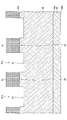
また、本実施形態における半導体装置の製造方法は、上記の図7に示す工程の後、熱エッチングを行い、この後、pボディ領域33を形成するためのイオン注入を行い、再度熱エッチングを行うものであってもよい。具体的には、図7に示す工程の後、イオン注入マスク63を除去し、図17に示すように、熱エッチングマスク65を形成し、熱エッチングを行う。これにより、凹部21と凸部22の間に、傾斜面23を形成する。
また、本実施形態における半導体装置の製造方法は、上記の図7に示す工程の後、熱エッチングを行い、この後、pボディ領域33を形成するためのイオン注入を行い、再度熱エッチングを行うものであってもよい。具体的には、図7に示す工程の後、イオン注入マスク63を除去し、図17に示すように、熱エッチングマスク65を形成し、熱エッチングを行う。これにより、凹部21と凸部22の間に、傾斜面23を形成する。
次に、図18に示すように、凹部21の底面21aのn+コンタクト領域32よりも深い領域及び傾斜面23に、p型となる不純物元素をイオン注入することにより、pボディ領域33を形成する。これにより、熱エッチングマスク65と傾斜面23との間のnドリフト領域30とpボディ領域33との境界33aが、単結晶炭化珪素基板10の一方の主面10aに対し垂直に形成される。
次に、図19に示すように、再度熱エッチングを行う。これにより、熱エッチングマスク65の端の下側の部分においても、傾斜面23における半導体の一部が除去され、nドリフト領域30とpボディ領域33との境界は、傾斜面23に位置するように形成される。これにより、凹部21と凸部22の間に、{03-3-8}面となる傾斜面23を形成することができる。
この後、上記の図10に示す工程以降の工程を行うことにより、図20に示す構造の半導体装置を製造することができる。この半導体装置では、傾斜面23の下において、pボディ領域33とnドリフト領域30との境界が、階段状ではなく、傾斜した形状で形成されるため、電界集中を更に緩和させることができ、信頼性を向上させることができる。
(変形例2)
また、本実施形態における半導体装置は、図21に示すように、p+コンタクト領域31及びpボディ領域33も深い位置に、p領域34を形成した構造のものであってもよい。p領域34とp+コンタクト領域31及びpボディ領域33とは、p+コンタクト領域31及びpボディ領域33の最も深い位置で接している。この半導体装置においては、p型となる不純物元素の濃度は、p+コンタクト領域31<p領域34<pボディ領域33であることが好ましい。このようなp領域34を形成することにより、本実施形態において、トランジスタとともに形成される内蔵ダイオード(ボディダイオード)の順方向における抵抗を低くすることができる。尚、p領域34は、p型となる不純物元素をイオン注入することにより形成してもよく、単結晶炭化珪素基板10の一方の主面10aの上に、炭化珪素エピタキシャル層20を形成する際に、エピタキシャル成長の途中で、p領域34を形成してもよい。
また、本実施形態における半導体装置は、図21に示すように、p+コンタクト領域31及びpボディ領域33も深い位置に、p領域34を形成した構造のものであってもよい。p領域34とp+コンタクト領域31及びpボディ領域33とは、p+コンタクト領域31及びpボディ領域33の最も深い位置で接している。この半導体装置においては、p型となる不純物元素の濃度は、p+コンタクト領域31<p領域34<pボディ領域33であることが好ましい。このようなp領域34を形成することにより、本実施形態において、トランジスタとともに形成される内蔵ダイオード(ボディダイオード)の順方向における抵抗を低くすることができる。尚、p領域34は、p型となる不純物元素をイオン注入することにより形成してもよく、単結晶炭化珪素基板10の一方の主面10aの上に、炭化珪素エピタキシャル層20を形成する際に、エピタキシャル成長の途中で、p領域34を形成してもよい。
本開示によれば、チャネル移動度が高く、オン抵抗の低い炭化珪素を用いた半導体装置を提供できる。
今回開示された実施の形態はすべての点で例示であって、制限的なものではないと考えられるべきである。本発明の範囲は上記した説明ではなくて請求の範囲によって示され、請求の範囲と均等の意味、および範囲内でのすべての変更が含まれることが意図される。
10 単結晶炭化珪素基板
10a 一方の主面
10b 他方の主面
20 炭化珪素エピタキシャル層
20a 表面
21 凹部
21a 底面
22 凸部
22a 上面
23 傾斜面
23b 傾斜面と凸部との境界
30 nドリフト領域
31 p+コンタクト領域
32 n+コンタクト領域
33 pボディ領域
33a 境界
41 ゲート絶縁膜
42 ゲート電極
43 層間絶縁膜
44 ソース電極
45 ドレイン電極
10a 一方の主面
10b 他方の主面
20 炭化珪素エピタキシャル層
20a 表面
21 凹部
21a 底面
22 凸部
22a 上面
23 傾斜面
23b 傾斜面と凸部との境界
30 nドリフト領域
31 p+コンタクト領域
32 n+コンタクト領域
33 pボディ領域
33a 境界
41 ゲート絶縁膜
42 ゲート電極
43 層間絶縁膜
44 ソース電極
45 ドレイン電極
Claims (7)
- 単結晶炭化珪素基板と、
前記単結晶炭化珪素基板の一方の主面に形成された炭化珪素エピタキシャル層と、
前記炭化珪素エピタキシャル層の表面に形成された凹部及び凸部と、前記凹部と前記凸部との間に形成された傾斜面と、
前記凹部の底面の前記傾斜面側に形成された第1の導電型の第1のコンタクト領域と、
前記凹部の底面において前記第1のコンタクト領域と接する第2の導電型の第2のコンタクト領域と、
前記凸部の上面に形成された第1の導電型のドリフト領域と、
前記第1のコンタクト領域と前記ドリフト領域の間の前記傾斜面に形成された第2の導電型のボディ領域と、
前記傾斜面を覆うゲート絶縁膜と、
前記ゲート絶縁膜の上に形成されたゲート電極と、
前記第1のコンタクト領域及び前記第2のコンタクト領域の上に形成されたソース電極と、
前記単結晶炭化珪素基板の他方の主面に形成されたドレイン電極と、
を有し、
前記単結晶炭化珪素基板の一方の主面に対し、前記傾斜面の角度は、40°以上70°以下である半導体装置。 - 前記ドリフト領域と前記ボディ領域との境界は前記傾斜面に位置しており、
前記境界は、前記単結晶炭化珪素基板の一方の主面に対し垂直である請求項1に記載の半導体装置。 - 前記ボディ領域における不純物濃度は、1×1017cm-3以上3×1019cm-3以下である請求項1または2に記載の半導体装置。
- 前記炭化珪素エピタキシャル層における前記第2のコンタクト領域及び前記ボディ領域よりも深い位置には、前記ボディ領域よりも不純物濃度の高い第2の導電型の半導体領域が、前記第2のコンタクト領域及び前記ボディ領域と接して形成されている請求項1から3のいずれか一項に記載の半導体装置。
- 前記凹部の平面形状は、六角形である請求項1から4のいずれか一項に記載の半導体装置。
- 前記単結晶炭化珪素基板は4H型の結晶構造を有し、
前記炭化珪素エピタキシャル層は4H型の結晶構造を有する請求項1から5のいずれか一項に記載の半導体装置。 - 4H型の結晶構造を有する単結晶炭化珪素基板と、
4H型の結晶構造を有し、前記単結晶炭化珪素基板の一方の主面に形成された炭化珪素エピタキシャル層と、
前記炭化珪素エピタキシャル層の表面に形成された凹部及び凸部と、前記凹部と前記凸部との間に形成された傾斜面と、
前記凹部の底面の前記傾斜面側に形成された第1の導電型の第1のコンタクト領域と、
前記凹部の底面において前記第1のコンタクト領域と接する第2の導電型の第2のコンタクト領域と、
前記凸部の上面に形成された第1の導電型のドリフト領域と、
前記第1のコンタクト領域と前記ドリフト領域の間の前記傾斜面に形成された第2の導電型のボディ領域と、
前記傾斜面を覆うゲート絶縁膜と、
前記ゲート絶縁膜の上に形成されたゲート電極と、
前記第1のコンタクト領域及び前記第2のコンタクト領域の上に形成されたソース電極と、
前記単結晶炭化珪素基板の他方の主面に形成されたドレイン電極と、
を有し、
前記単結晶炭化珪素基板の一方の主面に対し、前記傾斜面の角度は、40°以上70°以下であり、
前記ドリフト領域と前記ボディ領域との境界は前記傾斜面に位置しており、
前記境界は、前記単結晶炭化珪素基板の一方の主面に対し垂直であり、
前記ボディ領域における不純物濃度は、1×1017cm-3以上3×1019cm-3以下である半導体装置。
Priority Applications (2)
| Application Number | Priority Date | Filing Date | Title |
|---|---|---|---|
| US16/349,775 US20190319102A1 (en) | 2016-11-25 | 2017-06-29 | Semiconductor device |
| JP2018552399A JPWO2018096722A1 (ja) | 2016-11-25 | 2017-06-29 | 半導体装置 |
Applications Claiming Priority (2)
| Application Number | Priority Date | Filing Date | Title |
|---|---|---|---|
| JP2016-229024 | 2016-11-25 | ||
| JP2016229024 | 2016-11-25 |
Publications (1)
| Publication Number | Publication Date |
|---|---|
| WO2018096722A1 true WO2018096722A1 (ja) | 2018-05-31 |
Family
ID=62195681
Family Applications (1)
| Application Number | Title | Priority Date | Filing Date |
|---|---|---|---|
| PCT/JP2017/024054 Ceased WO2018096722A1 (ja) | 2016-11-25 | 2017-06-29 | 半導体装置 |
Country Status (3)
| Country | Link |
|---|---|
| US (1) | US20190319102A1 (ja) |
| JP (1) | JPWO2018096722A1 (ja) |
| WO (1) | WO2018096722A1 (ja) |
Families Citing this family (3)
| Publication number | Priority date | Publication date | Assignee | Title |
|---|---|---|---|---|
| US12166082B2 (en) * | 2022-04-06 | 2024-12-10 | Leap Semiconductor Corp. | Silicon carbide semiconductor power transistor and method of manufacturing the same |
| US20230335595A1 (en) * | 2022-04-13 | 2023-10-19 | Leap Semiconductor Corp. | Silicon carbide semiconductor power transistor and method of manufacturing the same |
| CN115513297B (zh) * | 2022-11-09 | 2023-09-22 | 中芯越州集成电路制造(绍兴)有限公司 | 碳化硅平面mosfet器件及其制造方法 |
Citations (4)
| Publication number | Priority date | Publication date | Assignee | Title |
|---|---|---|---|---|
| WO2015056318A1 (ja) * | 2013-10-17 | 2015-04-23 | 三菱電機株式会社 | 炭化珪素半導体装置 |
| JP2015153854A (ja) * | 2014-02-13 | 2015-08-24 | 住友電気工業株式会社 | 炭化珪素半導体装置 |
| JP2016143788A (ja) * | 2015-02-03 | 2016-08-08 | 住友電気工業株式会社 | 炭化珪素半導体装置の製造方法 |
| JP2016195225A (ja) * | 2015-04-01 | 2016-11-17 | 富士電機株式会社 | 炭化ケイ素半導体装置及びその処理方法 |
Family Cites Families (3)
| Publication number | Priority date | Publication date | Assignee | Title |
|---|---|---|---|---|
| JP4049095B2 (ja) * | 2003-12-25 | 2008-02-20 | 日産自動車株式会社 | 半導体装置及びその製造方法 |
| JP5234927B2 (ja) * | 2008-05-22 | 2013-07-10 | 株式会社豊田中央研究所 | 半導体装置の製造方法 |
| JP5757223B2 (ja) * | 2011-12-02 | 2015-07-29 | 住友電気工業株式会社 | 炭化珪素半導体装置およびその製造方法 |
-
2017
- 2017-06-29 US US16/349,775 patent/US20190319102A1/en not_active Abandoned
- 2017-06-29 JP JP2018552399A patent/JPWO2018096722A1/ja active Pending
- 2017-06-29 WO PCT/JP2017/024054 patent/WO2018096722A1/ja not_active Ceased
Patent Citations (4)
| Publication number | Priority date | Publication date | Assignee | Title |
|---|---|---|---|---|
| WO2015056318A1 (ja) * | 2013-10-17 | 2015-04-23 | 三菱電機株式会社 | 炭化珪素半導体装置 |
| JP2015153854A (ja) * | 2014-02-13 | 2015-08-24 | 住友電気工業株式会社 | 炭化珪素半導体装置 |
| JP2016143788A (ja) * | 2015-02-03 | 2016-08-08 | 住友電気工業株式会社 | 炭化珪素半導体装置の製造方法 |
| JP2016195225A (ja) * | 2015-04-01 | 2016-11-17 | 富士電機株式会社 | 炭化ケイ素半導体装置及びその処理方法 |
Also Published As
| Publication number | Publication date |
|---|---|
| US20190319102A1 (en) | 2019-10-17 |
| JPWO2018096722A1 (ja) | 2019-10-17 |
Similar Documents
| Publication | Publication Date | Title |
|---|---|---|
| JP5668576B2 (ja) | 炭化珪素半導体装置 | |
| JP5741584B2 (ja) | 半導体装置の製造方法 | |
| CN103782391B (zh) | 碳化硅半导体器件及其制造方法 | |
| JP5699878B2 (ja) | 炭化珪素半導体装置およびその製造方法 | |
| JP5764046B2 (ja) | 炭化珪素半導体装置の製造方法 | |
| CN103247680A (zh) | 碳化硅半导体器件和制造碳化硅半导体器件的方法 | |
| JP2015060859A (ja) | 炭化珪素半導体装置および炭化珪素半導体装置の製造方法 | |
| CN103258721A (zh) | 制造碳化硅半导体器件的方法和碳化硅半导体器件 | |
| JP6098474B2 (ja) | 炭化珪素半導体装置およびその製造方法 | |
| CN103339731A (zh) | 具有过度生长的发射极的SiC双极结晶体管 | |
| US9806167B2 (en) | Method for manufacturing silicon carbide semiconductor device | |
| JP5867134B2 (ja) | 炭化珪素半導体装置の製造方法 | |
| JPWO2018096722A1 (ja) | 半導体装置 | |
| JP5875334B2 (ja) | 炭化珪素半導体装置 | |
| KR102100863B1 (ko) | SiC MOSFET 전력 반도체 소자 | |
| JP6256075B2 (ja) | 炭化珪素半導体装置 | |
| US20160133707A1 (en) | Silicon carbide semiconductor device and method for manufacturing same | |
| JP2022052774A (ja) | 炭化珪素半導体装置 | |
| JP6233436B2 (ja) | 炭化珪素半導体装置の製造方法 | |
| JP2014033031A (ja) | 炭化珪素半導体装置およびその製造方法 | |
| WO2015037335A1 (ja) | 炭化珪素半導体装置およびその製造方法 | |
| JP2013172119A (ja) | 炭化珪素半導体装置およびその製造方法 |
Legal Events
| Date | Code | Title | Description |
|---|---|---|---|
| 121 | Ep: the epo has been informed by wipo that ep was designated in this application |
Ref document number: 17874113 Country of ref document: EP Kind code of ref document: A1 |
|
| ENP | Entry into the national phase |
Ref document number: 2018552399 Country of ref document: JP Kind code of ref document: A |
|
| NENP | Non-entry into the national phase |
Ref country code: DE |
|
| 122 | Ep: pct application non-entry in european phase |
Ref document number: 17874113 Country of ref document: EP Kind code of ref document: A1 |