WO2018096714A1 - 帯電部材 - Google Patents
帯電部材 Download PDFInfo
- Publication number
- WO2018096714A1 WO2018096714A1 PCT/JP2017/019760 JP2017019760W WO2018096714A1 WO 2018096714 A1 WO2018096714 A1 WO 2018096714A1 JP 2017019760 W JP2017019760 W JP 2017019760W WO 2018096714 A1 WO2018096714 A1 WO 2018096714A1
- Authority
- WO
- WIPO (PCT)
- Prior art keywords
- conductive
- charging member
- particles
- member according
- resin
- Prior art date
- Legal status (The legal status is an assumption and is not a legal conclusion. Google has not performed a legal analysis and makes no representation as to the accuracy of the status listed.)
- Ceased
Links
Images


Classifications
-
- B—PERFORMING OPERATIONS; TRANSPORTING
- B32—LAYERED PRODUCTS
- B32B—LAYERED PRODUCTS, i.e. PRODUCTS BUILT-UP OF STRATA OF FLAT OR NON-FLAT, e.g. CELLULAR OR HONEYCOMB, FORM
- B32B15/00—Layered products comprising a layer of metal
- B32B15/04—Layered products comprising a layer of metal comprising metal as the main or only constituent of a layer, which is next to another layer of the same or of a different material
- B32B15/08—Layered products comprising a layer of metal comprising metal as the main or only constituent of a layer, which is next to another layer of the same or of a different material of synthetic resin
- B32B15/088—Layered products comprising a layer of metal comprising metal as the main or only constituent of a layer, which is next to another layer of the same or of a different material of synthetic resin comprising polyamides
-
- G—PHYSICS
- G03—PHOTOGRAPHY; CINEMATOGRAPHY; ANALOGOUS TECHNIQUES USING WAVES OTHER THAN OPTICAL WAVES; ELECTROGRAPHY; HOLOGRAPHY
- G03G—ELECTROGRAPHY; ELECTROPHOTOGRAPHY; MAGNETOGRAPHY
- G03G15/00—Apparatus for electrographic processes using a charge pattern
- G03G15/02—Apparatus for electrographic processes using a charge pattern for laying down a uniform charge, e.g. for sensitising; Corona discharge devices
- G03G15/0208—Apparatus for electrographic processes using a charge pattern for laying down a uniform charge, e.g. for sensitising; Corona discharge devices by contact, friction or induction, e.g. liquid charging apparatus
- G03G15/0216—Apparatus for electrographic processes using a charge pattern for laying down a uniform charge, e.g. for sensitising; Corona discharge devices by contact, friction or induction, e.g. liquid charging apparatus by bringing a charging member into contact with the member to be charged, e.g. roller, brush chargers
- G03G15/0233—Structure, details of the charging member, e.g. chemical composition, surface properties
-
- B—PERFORMING OPERATIONS; TRANSPORTING
- B29—WORKING OF PLASTICS; WORKING OF SUBSTANCES IN A PLASTIC STATE IN GENERAL
- B29C—SHAPING OR JOINING OF PLASTICS; SHAPING OF MATERIAL IN A PLASTIC STATE, NOT OTHERWISE PROVIDED FOR; AFTER-TREATMENT OF THE SHAPED PRODUCTS, e.g. REPAIRING
- B29C35/00—Heating, cooling or curing, e.g. crosslinking or vulcanising; Apparatus therefor
- B29C35/02—Heating or curing, e.g. crosslinking or vulcanizing during moulding, e.g. in a mould
-
- B—PERFORMING OPERATIONS; TRANSPORTING
- B32—LAYERED PRODUCTS
- B32B—LAYERED PRODUCTS, i.e. PRODUCTS BUILT-UP OF STRATA OF FLAT OR NON-FLAT, e.g. CELLULAR OR HONEYCOMB, FORM
- B32B15/00—Layered products comprising a layer of metal
- B32B15/04—Layered products comprising a layer of metal comprising metal as the main or only constituent of a layer, which is next to another layer of the same or of a different material
- B32B15/06—Layered products comprising a layer of metal comprising metal as the main or only constituent of a layer, which is next to another layer of the same or of a different material of natural rubber or synthetic rubber
-
- B—PERFORMING OPERATIONS; TRANSPORTING
- B32—LAYERED PRODUCTS
- B32B—LAYERED PRODUCTS, i.e. PRODUCTS BUILT-UP OF STRATA OF FLAT OR NON-FLAT, e.g. CELLULAR OR HONEYCOMB, FORM
- B32B15/00—Layered products comprising a layer of metal
- B32B15/04—Layered products comprising a layer of metal comprising metal as the main or only constituent of a layer, which is next to another layer of the same or of a different material
- B32B15/08—Layered products comprising a layer of metal comprising metal as the main or only constituent of a layer, which is next to another layer of the same or of a different material of synthetic resin
-
- B—PERFORMING OPERATIONS; TRANSPORTING
- B32—LAYERED PRODUCTS
- B32B—LAYERED PRODUCTS, i.e. PRODUCTS BUILT-UP OF STRATA OF FLAT OR NON-FLAT, e.g. CELLULAR OR HONEYCOMB, FORM
- B32B15/00—Layered products comprising a layer of metal
- B32B15/04—Layered products comprising a layer of metal comprising metal as the main or only constituent of a layer, which is next to another layer of the same or of a different material
- B32B15/08—Layered products comprising a layer of metal comprising metal as the main or only constituent of a layer, which is next to another layer of the same or of a different material of synthetic resin
- B32B15/095—Layered products comprising a layer of metal comprising metal as the main or only constituent of a layer, which is next to another layer of the same or of a different material of synthetic resin comprising polyurethanes
-
- B—PERFORMING OPERATIONS; TRANSPORTING
- B32—LAYERED PRODUCTS
- B32B—LAYERED PRODUCTS, i.e. PRODUCTS BUILT-UP OF STRATA OF FLAT OR NON-FLAT, e.g. CELLULAR OR HONEYCOMB, FORM
- B32B15/00—Layered products comprising a layer of metal
- B32B15/18—Layered products comprising a layer of metal comprising iron or steel
-
- B—PERFORMING OPERATIONS; TRANSPORTING
- B32—LAYERED PRODUCTS
- B32B—LAYERED PRODUCTS, i.e. PRODUCTS BUILT-UP OF STRATA OF FLAT OR NON-FLAT, e.g. CELLULAR OR HONEYCOMB, FORM
- B32B15/00—Layered products comprising a layer of metal
- B32B15/20—Layered products comprising a layer of metal comprising aluminium or copper
-
- B—PERFORMING OPERATIONS; TRANSPORTING
- B32—LAYERED PRODUCTS
- B32B—LAYERED PRODUCTS, i.e. PRODUCTS BUILT-UP OF STRATA OF FLAT OR NON-FLAT, e.g. CELLULAR OR HONEYCOMB, FORM
- B32B25/00—Layered products comprising a layer of natural or synthetic rubber
- B32B25/02—Layered products comprising a layer of natural or synthetic rubber with fibres or particles being present as additives in the layer
-
- B—PERFORMING OPERATIONS; TRANSPORTING
- B32—LAYERED PRODUCTS
- B32B—LAYERED PRODUCTS, i.e. PRODUCTS BUILT-UP OF STRATA OF FLAT OR NON-FLAT, e.g. CELLULAR OR HONEYCOMB, FORM
- B32B25/00—Layered products comprising a layer of natural or synthetic rubber
- B32B25/12—Layered products comprising a layer of natural or synthetic rubber comprising natural rubber
-
- B—PERFORMING OPERATIONS; TRANSPORTING
- B32—LAYERED PRODUCTS
- B32B—LAYERED PRODUCTS, i.e. PRODUCTS BUILT-UP OF STRATA OF FLAT OR NON-FLAT, e.g. CELLULAR OR HONEYCOMB, FORM
- B32B25/00—Layered products comprising a layer of natural or synthetic rubber
- B32B25/14—Layered products comprising a layer of natural or synthetic rubber comprising synthetic rubber copolymers
-
- B—PERFORMING OPERATIONS; TRANSPORTING
- B32—LAYERED PRODUCTS
- B32B—LAYERED PRODUCTS, i.e. PRODUCTS BUILT-UP OF STRATA OF FLAT OR NON-FLAT, e.g. CELLULAR OR HONEYCOMB, FORM
- B32B25/00—Layered products comprising a layer of natural or synthetic rubber
- B32B25/16—Layered products comprising a layer of natural or synthetic rubber comprising polydienes homopolymers or poly-halodienes homopolymers
-
- B—PERFORMING OPERATIONS; TRANSPORTING
- B32—LAYERED PRODUCTS
- B32B—LAYERED PRODUCTS, i.e. PRODUCTS BUILT-UP OF STRATA OF FLAT OR NON-FLAT, e.g. CELLULAR OR HONEYCOMB, FORM
- B32B25/00—Layered products comprising a layer of natural or synthetic rubber
- B32B25/20—Layered products comprising a layer of natural or synthetic rubber comprising silicone rubber
-
- B—PERFORMING OPERATIONS; TRANSPORTING
- B32—LAYERED PRODUCTS
- B32B—LAYERED PRODUCTS, i.e. PRODUCTS BUILT-UP OF STRATA OF FLAT OR NON-FLAT, e.g. CELLULAR OR HONEYCOMB, FORM
- B32B27/00—Layered products comprising a layer of synthetic resin
- B32B27/18—Layered products comprising a layer of synthetic resin characterised by the use of special additives
-
- B—PERFORMING OPERATIONS; TRANSPORTING
- B32—LAYERED PRODUCTS
- B32B—LAYERED PRODUCTS, i.e. PRODUCTS BUILT-UP OF STRATA OF FLAT OR NON-FLAT, e.g. CELLULAR OR HONEYCOMB, FORM
- B32B27/00—Layered products comprising a layer of synthetic resin
- B32B27/28—Layered products comprising a layer of synthetic resin comprising synthetic resins not wholly covered by any one of the sub-groups B32B27/30 - B32B27/42
- B32B27/283—Layered products comprising a layer of synthetic resin comprising synthetic resins not wholly covered by any one of the sub-groups B32B27/30 - B32B27/42 comprising polysiloxanes
-
- B—PERFORMING OPERATIONS; TRANSPORTING
- B32—LAYERED PRODUCTS
- B32B—LAYERED PRODUCTS, i.e. PRODUCTS BUILT-UP OF STRATA OF FLAT OR NON-FLAT, e.g. CELLULAR OR HONEYCOMB, FORM
- B32B27/00—Layered products comprising a layer of synthetic resin
- B32B27/34—Layered products comprising a layer of synthetic resin comprising polyamides
-
- B—PERFORMING OPERATIONS; TRANSPORTING
- B32—LAYERED PRODUCTS
- B32B—LAYERED PRODUCTS, i.e. PRODUCTS BUILT-UP OF STRATA OF FLAT OR NON-FLAT, e.g. CELLULAR OR HONEYCOMB, FORM
- B32B27/00—Layered products comprising a layer of synthetic resin
- B32B27/40—Layered products comprising a layer of synthetic resin comprising polyurethanes
-
- B—PERFORMING OPERATIONS; TRANSPORTING
- B32—LAYERED PRODUCTS
- B32B—LAYERED PRODUCTS, i.e. PRODUCTS BUILT-UP OF STRATA OF FLAT OR NON-FLAT, e.g. CELLULAR OR HONEYCOMB, FORM
- B32B7/00—Layered products characterised by the relation between layers; Layered products characterised by the relative orientation of features between layers, or by the relative values of a measurable parameter between layers, i.e. products comprising layers having different physical, chemical or physicochemical properties; Layered products characterised by the interconnection of layers
- B32B7/04—Interconnection of layers
- B32B7/12—Interconnection of layers using interposed adhesives or interposed materials with bonding properties
-
- F—MECHANICAL ENGINEERING; LIGHTING; HEATING; WEAPONS; BLASTING
- F16—ENGINEERING ELEMENTS AND UNITS; GENERAL MEASURES FOR PRODUCING AND MAINTAINING EFFECTIVE FUNCTIONING OF MACHINES OR INSTALLATIONS; THERMAL INSULATION IN GENERAL
- F16C—SHAFTS; FLEXIBLE SHAFTS; ELEMENTS OR CRANKSHAFT MECHANISMS; ROTARY BODIES OTHER THAN GEARING ELEMENTS; BEARINGS
- F16C13/00—Rolls, drums, discs, or the like; Bearings or mountings therefor
-
- G—PHYSICS
- G03—PHOTOGRAPHY; CINEMATOGRAPHY; ANALOGOUS TECHNIQUES USING WAVES OTHER THAN OPTICAL WAVES; ELECTROGRAPHY; HOLOGRAPHY
- G03G—ELECTROGRAPHY; ELECTROPHOTOGRAPHY; MAGNETOGRAPHY
- G03G9/00—Developers
- G03G9/08—Developers with toner particles
-
- B—PERFORMING OPERATIONS; TRANSPORTING
- B32—LAYERED PRODUCTS
- B32B—LAYERED PRODUCTS, i.e. PRODUCTS BUILT-UP OF STRATA OF FLAT OR NON-FLAT, e.g. CELLULAR OR HONEYCOMB, FORM
- B32B2255/00—Coating on the layer surface
- B32B2255/10—Coating on the layer surface on synthetic resin layer or on natural or synthetic rubber layer
-
- B—PERFORMING OPERATIONS; TRANSPORTING
- B32—LAYERED PRODUCTS
- B32B—LAYERED PRODUCTS, i.e. PRODUCTS BUILT-UP OF STRATA OF FLAT OR NON-FLAT, e.g. CELLULAR OR HONEYCOMB, FORM
- B32B2255/00—Coating on the layer surface
- B32B2255/26—Polymeric coating
-
- B—PERFORMING OPERATIONS; TRANSPORTING
- B32—LAYERED PRODUCTS
- B32B—LAYERED PRODUCTS, i.e. PRODUCTS BUILT-UP OF STRATA OF FLAT OR NON-FLAT, e.g. CELLULAR OR HONEYCOMB, FORM
- B32B2264/00—Composition or properties of particles which form a particulate layer or are present as additives
- B32B2264/10—Inorganic particles
- B32B2264/102—Oxide or hydroxide
-
- B—PERFORMING OPERATIONS; TRANSPORTING
- B32—LAYERED PRODUCTS
- B32B—LAYERED PRODUCTS, i.e. PRODUCTS BUILT-UP OF STRATA OF FLAT OR NON-FLAT, e.g. CELLULAR OR HONEYCOMB, FORM
- B32B2264/00—Composition or properties of particles which form a particulate layer or are present as additives
- B32B2264/10—Inorganic particles
- B32B2264/107—Ceramic
- B32B2264/108—Carbon, e.g. graphite particles
-
- B—PERFORMING OPERATIONS; TRANSPORTING
- B32—LAYERED PRODUCTS
- B32B—LAYERED PRODUCTS, i.e. PRODUCTS BUILT-UP OF STRATA OF FLAT OR NON-FLAT, e.g. CELLULAR OR HONEYCOMB, FORM
- B32B2307/00—Properties of the layers or laminate
- B32B2307/20—Properties of the layers or laminate having particular electrical or magnetic properties, e.g. piezoelectric
- B32B2307/202—Conductive
-
- B—PERFORMING OPERATIONS; TRANSPORTING
- B32—LAYERED PRODUCTS
- B32B—LAYERED PRODUCTS, i.e. PRODUCTS BUILT-UP OF STRATA OF FLAT OR NON-FLAT, e.g. CELLULAR OR HONEYCOMB, FORM
- B32B2307/00—Properties of the layers or laminate
- B32B2307/50—Properties of the layers or laminate having particular mechanical properties
- B32B2307/538—Roughness
-
- B—PERFORMING OPERATIONS; TRANSPORTING
- B32—LAYERED PRODUCTS
- B32B—LAYERED PRODUCTS, i.e. PRODUCTS BUILT-UP OF STRATA OF FLAT OR NON-FLAT, e.g. CELLULAR OR HONEYCOMB, FORM
- B32B2457/00—Electrical equipment
Definitions
- the present invention relates to a charging member. More specifically, the present invention relates to a charging member that charges a latent image holding member such as a photosensitive member used in an electrostatic latent image process in a copying machine, a printer, or the like.
- a latent image holding member such as a photosensitive member used in an electrostatic latent image process in a copying machine, a printer, or the like.
- an “AC charging method” in which a voltage obtained by superimposing an AC voltage component (AC voltage component) on a DC voltage component is applied to a contact charging member.
- AC voltage component AC voltage component
- Vth discharge start voltage
- an AC power supply is required in addition to the DC power supply, which increases the cost of the device itself. It is.
- a large amount of proximity discharge is generated between the charging roller and the photosensitive member, the durability of the charging roller and the photosensitive member is lowered, and the photosensitive member is particularly easily worn.
- the conventional charging member is not sufficiently capable of uniformly forming dots while uniformly charging the photoreceptor over a long period of time.
- an object of the present invention is to provide a charging member having stable charging uniformity over a long period of time and excellent dot uniformity even when only a DC voltage is applied.
- the present invention provides a charging member comprising a conductive support, a conductive elastic layer laminated on the conductive support, and a conductive resin layer laminated as the outermost layer on the conductive elastic layer.
- the conductive resin layer includes a matrix material and resin particles, and the charging member in which the arithmetic average roughness Ra, the ten-point average roughness Rzjis, and the skewness Rsk in the conductive resin layer satisfy the following expressions, respectively: provide.
- Such a charging member has stable charging uniformity over a long period of time and excellent dot uniformity even when only a DC voltage is applied. 2.0 ⁇ Ra [ ⁇ m] ⁇ 7.0 15 ⁇ Rzjis [ ⁇ m] ⁇ 40 0.5 ⁇ Rsk ⁇ 2.5
- an average particle diameter B 2 having an average particle diameter B 1 and the second particles of the first particle satisfies the following equation . This makes it easier to maintain stable charging characteristics and dot uniformity.
- the layer thickness A of the part formed only by the matrix material in a conductive resin layer satisfy
- the interparticle distance RSm of the resin particles in the conductive resin layer preferably satisfies the following formula. This makes it easier to maintain stable charging characteristics and dot uniformity. 50 ⁇ RSm [ ⁇ m] ⁇ 250
- arithmetic mean roughness Ra in a conductive resin layer satisfy
- the ten-point average roughness Rzjis in the conductive resin layer preferably satisfies the following formula. This makes it easier to maintain stable charging characteristics and dot uniformity. 20 ⁇ Rzjis [ ⁇ m] ⁇ 35
- the skewness Rsk in the conductive resin layer preferably satisfies the following formula. This makes it easier to maintain stable charging characteristics and dot uniformity. 0.8 ⁇ Rsk ⁇ 2.0
- the resin particles are preferably insulating particles. This makes it easier to maintain stable charging characteristics and dot uniformity.
- the content of the resin particles is preferably 5 to 80 parts by mass with respect to 100 parts by mass of the matrix material. This makes it easier to maintain stable charging characteristics and dot uniformity.
- the resin particles are preferably amorphous particles. Since such particles have good affinity with the matrix material, the adhesion strength at the interface between the matrix material and the resin particles can be increased, and the durability can be further improved.
- the resin particles are preferably nylon resin particles. Since such particles have good affinity with the matrix material, the adhesion strength at the interface between the matrix material and the resin particles can be increased, and the durability can be further improved.
- the matrix material preferably contains at least one selected from the group consisting of nylon resin and polyurethane resin. Since these materials have good affinity with the resin particles, the same effect as described above, that is, the adhesion strength at the interface between the matrix material and the resin particles can be increased, and the durability can be further improved.
- the conductive elastic layer contains epichlorohydrin rubber. Thereby, defects due to resistance fluctuations during production can be reduced, so that productivity can be further improved. Moreover, the adhesive force of a conductive elastic body layer and a conductive resin layer can be improved more.
- a charging member having stable charging uniformity over a long period of time and excellent dot uniformity can be provided.
- Skewness represents the cube average of Z (x) at a reference length made dimensionless by the cube of the root mean square height (Zq).
- Zq root mean square height
- skewness is a parameter closely related to tribology (friction), but as a result of extensive studies, it has been found that skewness is an important parameter in the uniformity of discharge characteristics on the photoreceptor.
- the charging member of this embodiment includes a conductive support, a conductive elastic layer laminated on the conductive support, and a conductive resin layer laminated as the outermost layer on the conductive elastic layer.
- FIG. 1 is a schematic cross-sectional view of a charging member according to the present embodiment.
- the charging member 10 includes a conductive elastic body layer 2, a conductive resin layer 3, and the like on the outer peripheral surface of a conductive support (shaft body) 1 from the inner side to the outer side in the roll radial direction.
- shaft body a conductive support
- FIG. 1 is a schematic diagram to the last, for example, an intermediate layer such as a resistance adjustment layer for enhancing voltage resistance (leakage resistance) is interposed between the conductive elastic layer and the conductive resin layer. This aspect is not excluded.
- a charging member as shown in FIG. 1 is provided as a charging means for a member to be charged. Specifically, as a means for uniformly charging the surface of a photoconductor as an image carrier. Function.
- the conductive support is not particularly limited as long as it is made of a conductive metal.
- a metal hollow body made of iron, copper, aluminum, nickel, stainless steel, etc.
- a solid (rod-like) or the like is used.
- the outer peripheral surface of the conductive support may be subjected to a plating treatment as necessary for the purpose of providing rust prevention and scratch resistance as long as the conductivity is not impaired.
- the adhesive agent, a primer, etc. may be apply
- the conductive support has a cylindrical shape with a diameter of 5 to 10 mm and a length of 250 to 360 mm, for example.
- the conductive elastic layer is not particularly limited as long as it has an appropriate elasticity in order to ensure uniform adhesion to the photosensitive member.
- natural rubber ethylene-propylene-diene rubber (EPDM), styrene-butadiene rubber (SBR), silicone rubber, polyurethane elastomer, epichlorohydrin rubber, isoprene rubber (IR), butadiene rubber (BR), acrylonitrile-butadiene rubber (NBR), hydrogenated NBR (H-NBR) , Synthetic rubber such as chloroprene rubber (CR); synthetic resin such as polyamide resin, polyurethane resin, and silicone resin; and the like as a base polymer. These may be used alone or in combination of two or more.
- the conductive elastic layer preferably contains epichlorohydrin rubber as a main component. More specifically, the conductive elastic layer preferably contains 50% by mass or more of epichlorohydrin rubber, more preferably 80% by mass or more.
- the conductive agent carbon black, graphite, potassium titanate, iron oxide, conductive titanium oxide (c-TiO 2 ), conductive zinc oxide (c-ZnO), conductive tin oxide (c-SnO 2 ) And quaternary ammonium salts.
- the vulcanizing agent include sulfur.
- the vulcanization accelerator include tetramethyl thiuram disulfide (CZ).
- the lubricant include stearic acid.
- the auxiliary agent include zinc white (ZnO).
- the thickness of the conductive elastic layer is preferably about 1.25 to 3.00 mm in order to exhibit appropriate elasticity.
- the conductive resin layer contains a matrix material and resin particles.
- the resin particles contain first particles and second particles.
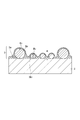
- FIG. 2 is an enlarged schematic cross-sectional view showing the surface of the conductive resin layer of the charging member according to this embodiment.
- the conductive resin layer 3 has a material (matrix material) 3a constituting a matrix and a plurality of first particles 3b 1 and second particles 3b 2 dispersed in the material. Yes.
- the matrix material is not particularly limited as long as it does not contaminate the photoreceptor to be charged.
- Fluorine resin, polyamide resin, acrylic resin, nylon resin, polyurethane resin, silicone resin, butyral resin, styrene- Examples thereof include base polymers such as ethylene / butylene-olefin copolymer (SEBC) and olefin-ethylene / butylene-olefin copolymer (CEBC). These may be used alone or in combination of two or more.
- the matrix material is at least selected from the group consisting of a fluororesin, an acrylic resin, a nylon resin, a polyurethane resin, and a silicone resin from the viewpoint of ease of handling, the degree of freedom in material design, and the like.
- a fluororesin an acrylic resin
- nylon resin a polyurethane resin
- silicone resin a silicone resin from the viewpoint of ease of handling, the degree of freedom in material design, and the like.
- One type is preferable, and at least one type selected from the group consisting of nylon resin and polyurethane resin is more preferable.
- the thickness of the conductive resin layer that is, the layer thickness A (layer thickness) of the portion formed of the matrix material alone is preferably 1.0 to 7.0 ⁇ m (“A” in FIG. 2). "portion). More specifically, the thickness of the conductive resin layer is the thickness at the midpoint between the nearest particles. When the thickness is 1.0 ⁇ m or more, the resin particles to be added are easily retained continuously without dropping off, and on the other hand, when the thickness is 7.0 ⁇ m or less, the charging performance is maintained well. It becomes easy to do. From such a viewpoint, the thickness of the conductive resin layer is more preferably 1.0 to 5.0 ⁇ m, and further preferably 2.0 to 4.0 ⁇ m. The thickness of the conductive resin layer can be measured by cutting the roller cross section with a sharp blade and observing with an optical microscope or an electron microscope.
- the resin particles are not particularly limited as long as the resin particles can form irregularities on the surface of the conductive resin layer in order to ensure a sufficient discharge point.
- Suitable materials for the resin particles include urethane resin, polyamide resin, fluororesin, nylon resin, acrylic resin, urea resin and the like. These may be used alone or in combination of two or more.
- the resin particles are nylon resin particles, acrylic resin particles, and polyamide resins from the viewpoints of compatibility with the matrix material, dispersion retention after adding the particles, stability after coating (pot life), and the like. It is preferably at least one selected from the group consisting of particles, and more preferably nylon resin particles.
- the resin particles are preferably insulating particles.
- the shape of the resin particles is not particularly limited as long as it can form irregularities on the surface of the conductive resin layer, and may be a true sphere, an oval sphere, an indefinite shape, or the like. However, it is preferable to use indeterminate resin particles from the viewpoint of preventing the resin particles from falling off.
- the average particle diameter of the first particles is preferably 20 to 40 ⁇ m from the viewpoint of suppressing charging unevenness which is an initial image defect (“B 1 ” portion in FIG. 2). From the same viewpoint, the average particle diameter of the first particles is more preferably 25 to 35 ⁇ m. Further, from the viewpoint of suppressing charging unevenness, the difference B 1 -B 2 between the average particle diameter B 1 of the first particles and the average particle diameter B 2 of the second particles (“B 2 ” portion in FIG. 2) is It is preferable that it is 10 micrometers or more. From the same viewpoint, the difference B 1 -B 2 is more preferably 12 ⁇ m or more, and further preferably 15 ⁇ m or more. The upper limit of B 1 -B 2 is not particularly limited, but can be 35 ⁇ m or less from the viewpoint of improving the potential difference when discharging at the tip of each particle.
- the average particle size of the particles can be derived by arbitrarily extracting 100 particles from a population of a plurality of particles by SEM observation and taking the average value of the particle sizes.
- the particle shape is not a perfect sphere and the particle diameter is not uniform, such as an elliptical sphere (a sphere with an elliptical cross section) or an indeterminate shape
- the simple average value of the longest diameter and the shortest diameter is the particle size.
- the particle diameter can be made as follows.
- the interparticle distance RSm of the resin particles (that is, the interparticle distance in all resin particles including the first particles and the second particles) is preferably 50 to 250 ⁇ m.
- the interparticle distance is preferably 80 to 200 ⁇ m, and more preferably 100 to 180 ⁇ m.
- the interparticle distance can be measured according to JIS B0601-2001.
- the ratio B 1 / A between the layer thickness A [ ⁇ m] of the conductive resin layer and the average particle diameter B 1 [ ⁇ m] of the first particles is 5.0 to 30.0. It is preferable.
- B 1 / A is 5.0 or more, it becomes easy to ensure charging uniformity.
- B 1 / A is 30.0 or less, improvement in the coating property of the coating liquid for forming the conductive resin layer and particles It becomes easy to suppress omission.
- B 1 / A is more preferably 7.5 to 20.0, and further preferably 8.0 to 12.5.
- the content of the resin particles is preferably 5 to 80 parts by mass, that is, 5 to 80 phr with respect to 100 parts by mass of the resin constituting the matrix material.
- the content is 5 phr or more, there is a tendency that the charging performance is more easily satisfied.
- the content is 80 phr or less, the particle sedimentation control when the paint is formed becomes easier and the coating stability is improved. There is a tendency not to get worse. From such a viewpoint, it is more preferably 10 to 70 phr.
- the ratio of the content of the first particles and the second particles in the resin particles is preferably 5: 1 to 1: 5. It is more preferably 1 to 1: 3.
- the content of particles contained in the conductive resin layer can be quantified as follows. For example, by sampling the conductive resin layer from the charging member and measuring the weight change (TG), differential heat (DTA), calorie (DSC), and mass of volatile components (MS) caused by heating it, The content of the particles can be quantified (TG-DTA-MS, DSC (thermal analysis)).
- conductive agents conductive carbon, graphite, copper, aluminum, nickel, iron powder, conductive tin oxide, conductive titanium oxide, ionic conductive agent, etc.
- a charge control agent or the like may be included as necessary.
- the arithmetic average roughness Ra of the surface of the conductive resin layer is 2.0 to 7.0 ⁇ m.
- the arithmetic average roughness is 2.0 or more, it becomes easy to ensure charging uniformity, and when it is 7.0 ⁇ m or less, contamination of the surface of the charging member due to toner, external additives and the like can be suppressed.
- the arithmetic average roughness Ra is preferably 2.5 ⁇ m or more and less than 7.0 ⁇ m, and more preferably 2.5 to 5.0 ⁇ m.
- the ten-point average roughness Rzjis on the surface of the conductive resin layer is 15 to 40 ⁇ m.
- the 10-point average roughness is 15 ⁇ m or more, the charging performance can be sufficiently secured, and when it is 40 ⁇ m or less, the stability of the paint can be obtained.
- the ten-point average roughness is preferably 20 to 35 ⁇ m, and more preferably 25 to 35 ⁇ m.
- the skewness Rsk on the surface of the conductive resin layer is 0.5 to 2.5.
- the skewness is preferably 0.8 to 2.0, and more preferably 0.8 to 1.5.
- the arithmetic average roughness, ten-point average roughness and skewness of the surface of the conductive resin layer were measured according to JIS B0601-2001 using a surface roughness measuring instrument SE-3400 manufactured by Kosaka Laboratory. can do. Further, the surface properties of the conductive resin layer including these characteristics can be adjusted by changing the size, amount, etc. of the particles added to the conductive resin layer.
- the charging member of this embodiment can maintain stable charging uniformity and dot uniformity over a long period even when only a DC voltage is applied.
- the bias voltage applied during image output until the lifetime of the photosensitive member is ⁇ 1000 to ⁇ 1500 V.
- charging performance under various environments can be maintained, and image density and various conditions can be easily controlled.
- the bias voltage is smaller than ⁇ 1500 V, it is difficult to optimize development conditions necessary for image formation.
- the bias voltage is greater than ⁇ 1000 V, excessive discharge is likely to occur in the particle portion of the conductive resin layer, and white spot-like image defects are likely to occur after image formation.
- the charging member of this embodiment as shown in FIG. 1 can be manufactured as follows, for example. That is, the material for the conductive elastic layer is kneaded using a kneader such as a kneader to prepare the material for the conductive elastic layer. Moreover, the coating material for conductive resin layers is prepared by kneading the material for conductive resin layers using a kneader such as a roll, adding an organic solvent to the mixture, mixing and stirring. Next, the material for the conductive elastic layer is filled in an injection mold in which a core metal serving as a conductive support is set, and heat crosslinking is performed under predetermined conditions.
- a kneader such as a kneader
- a base roll having a conductive elastic body layer formed along the outer peripheral surface of the conductive support is manufactured.
- a conductive resin layer is formed by applying a conductive resin layer coating solution on the outer peripheral surface of the base roll. In this way, a charging member in which a conductive elastic layer is formed on the outer peripheral surface of the conductive support and a conductive resin layer is formed on the outer peripheral surface of the conductive elastic layer can be manufactured.
- the method for forming the conductive elastic layer is not limited to the injection molding method, and a cast molding method or a method combining press molding and polishing may be employed.
- the coating method of the coating solution for the conductive resin layer is not particularly limited, and a conventionally known dipping method, spray coating method, roll coating method or the like may be employed.
- Example 1 (Preparation of conductive elastic layer forming material) 100.00 parts by mass of epichlorohydrin rubber (Daiso Co., Ltd., “Epichromer CG-102”) as a rubber component, 5.00 parts by mass of sorbitan fatty acid ester (Kao Co., Ltd., “Splendor R-300”) as a lubricant, softening 5.00 parts by mass of ricinoleic acid as an agent, 0.50 parts by mass of hydrotalcite compound (“DHT-4A”, manufactured by Kyowa Chemical Industry Co., Ltd.) as an acid acceptor, tetrabutylammonium chloride (ionic conductivity) as a conductive agent Agent) (Tokyo Chemical Industry Co., Ltd., “Tetrabutylammonium Chloride”) 1.00 parts by mass, Silica (Tosoh Silica Co., Ltd., “Nipsil ER”) 50.00 parts by mass as a filler, Cross-linking accelerator Zinc
- thermoplastic N-methoxymethylated 6-nylon manufactured by Nagase ChemteX Corp., “Toresin F-30K”
- methylenebisethylmethylaniline as a curing agent
- carbon black electroconductive agent
- amorphous nylon resin particles manufactured by Arkema, “Orgasol Series” having different average particle diameters as resin particles are added to the mixed solution in the amounts shown in Table 1, so that the solution is uniform. Stir until well. Then, each component in the solution was dispersed using two rolls. Thereby, the coating liquid for conductive resin layer formation was prepared.
- the average particle size of the resin particles was measured as follows. That is, 100 particles were arbitrarily extracted from the population of a plurality of particles by SEM observation, and the average value of the particle sizes was defined as the average particle size of the resin particles. Since the particle shape of the resin particles used was indefinite, the simple average value of the observed longest diameter and shortest diameter was taken as the particle diameter of each particle.
- a roll forming die having a cylindrical roll forming space was prepared, and a core metal having a diameter of 6 mm was set so as to be coaxial with the roll forming space.
- the conductive elastic layer forming material prepared as described above was poured into the roll forming space in which the metal core was set, heated at 170 ° C. for 30 minutes, then cooled and demolded. As a result, a conductive elastic body layer having a thickness of 3 mm formed along the outer peripheral surface of the cored bar as the conductive shaft body was obtained.
- the coating solution for forming a conductive resin layer prepared as described above was applied to the surface of the conductive elastic layer of the roll body by a roll coating method. At this time, coating was performed while removing unnecessary coating liquid with a scraper so as to obtain a desired film thickness. After forming the coating film, this was heated at 150 ° C. for 30 minutes to form a conductive resin layer having a thickness of 4.0 ⁇ m. Thereby, a shaft body (conductive support), a conductive elastic layer formed along the outer peripheral surface of the shaft body, a conductive resin layer formed along the outer peripheral surface of the conductive elastic layer, and A charging member having the following characteristics was prepared.
- a charging member was produced in the same manner as in Example 1 except that the thickness of the conductive resin layer, the kind of added particles, the amount added, and the like were changed and adjusted as shown in Table 1.
- amorphous nylon resin particles manufactured by Arkema, “Orgasol Series” were used as the resin particles.
- the particle addition amount [phr] indicates the addition amount (parts by mass) with respect to 100 parts by mass of the matrix material (N-methoxymethylated 6-nylon).
- the layer thickness A of the conductive resin layer was measured by measuring several places at a magnification of 5000 using a scanning electron microscope (SEM).
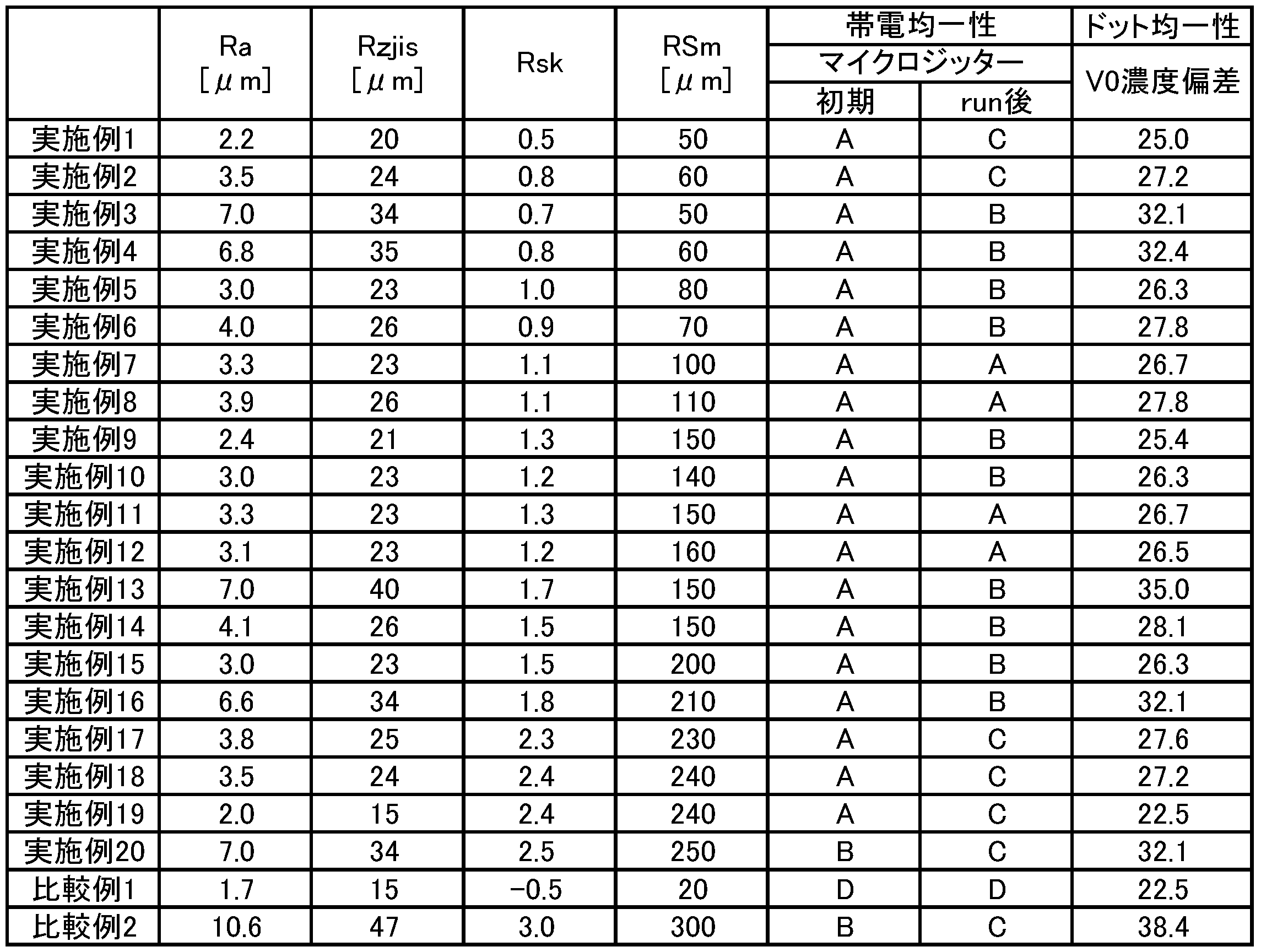
- Micro Jitter Evaluation A halftone image was output using the image forming apparatus. The micro jitter appearing in this image was visually observed and evaluated based on the following criteria. The evaluation results are shown in Table 2. Micro jitter is one of the indexes for evaluating charging uniformity. Micro jitter was observed at the initial stage of image formation (initial stage) and after the endurance test (after run) to determine whether stable charging uniformity over a long period of time was obtained. Evaluation A: A uniform halftone image was obtained. Evaluation B: A slight charge unevenness occurred at the edge of the image. Evaluation C: Uneven charging occurred clearly at the edge of the image. Evaluation D: Uneven charging occurred on the entire surface of the image.
- the obtained binarized image was divided into tiles each having a side of 44.4 ⁇ m (32 pixels) (32 ⁇ 24 divisions), the average density of each tile was determined, and the deviation was calculated from the density.
- FIG. 3 is a visualized image of the V0 density deviation on the photoconductor in (a) Example 1, (b) Example 8 and (c) Example 19.
- the image forming apparatus including the charging member according to the embodiment can exhibit stable charging uniformity and excellent dot uniformity over a long period even when only a DC voltage is applied.
- conductive support 1 ... conductive support, 2 ... conductive elastic layer, 3 ... conductive resin layer, 3a ... matrix material, 3b 1 ... first particle, 3b 2 ... second particle, 10 ... charging member.
Landscapes
- Physics & Mathematics (AREA)
- Engineering & Computer Science (AREA)
- General Physics & Mathematics (AREA)
- General Engineering & Computer Science (AREA)
- Plasma & Fusion (AREA)
- Health & Medical Sciences (AREA)
- Oral & Maxillofacial Surgery (AREA)
- Thermal Sciences (AREA)
- Mechanical Engineering (AREA)
- Electrostatic Charge, Transfer And Separation In Electrography (AREA)
Abstract
本発明は、導電性支持体と、導電性支持体上に積層された導電性弾性体層と、導電性弾性体層上に最外層として積層された導電性樹脂層とからなる帯電部材であって、導電性樹脂層はマトリックス材料及び樹脂粒子を含有し、導電性樹脂層における算術平均粗さが2.0≦Ra[μm]≦7.0、十点平均粗さが20≦Rzjis[μm]≦40、及びスキューネスが0.5≦Rsk≦2.5である、帯電部材に関する。
Description
本発明は帯電部材に関する。より具体的には、本発明は、複写機やプリンター等において、静電潜像プロセスに用いられる感光体等の潜像保持体を帯電させる帯電部材に関する。
従来、帯電均一性を改善するために、直流電圧成分に交流電圧成分(AC電圧成分)を重畳した電圧を接触帯電部材に印加する「AC帯電方式」が用いられている。しかしながら、直流電圧印加時における放電開始電圧(Vth)の2倍以上のピーク間電圧を有する高圧の交流電圧を重畳させるため、直流電源とは別に交流電源が必要となり、装置自体のコストアップを招いている。更には、帯電ローラと感光体の間で多量の近接放電が発生するため、帯電ローラ及び感光体の耐久性が低下し、特に感光体摩耗がし易いという問題がある。
これらの問題点は、帯電ローラに直流電圧のみを印加して帯電を行うことにより低減される。そこで、直流電圧のみを印加して帯電を行う場合に用いられる帯電部材の帯電特性を向上するべく、特に帯電部材の表面性状の観点から種々の検討がなされている(例えば、特許文献1及び2)。
しかしながら、従来の帯電部材は、長期にわたり感光体を均一に帯電させつつ、かつ均一にドットを形成する性能が十分とは言えないのが現状である。
そこで本発明は、直流電圧のみを印加する場合であっても、長期にわたり安定した帯電均一性を有しかつ優れたドット均一性を有する帯電部材を提供することを目的とする。
先行技術の問題点に鑑み、種々の検討を行った結果、帯電部材最外層の表面性状を従来の知見とは異なる範囲に調整することが、所望の特性の発現において極めて重要であることを見出し、本発明の完成に至った。
すなわち、本発明は、導電性支持体と、導電性支持体上に積層された導電性弾性体層と、導電性弾性体層上に最外層として積層された導電性樹脂層とからなる帯電部材であって、導電性樹脂層はマトリックス材料及び樹脂粒子を含有し、導電性樹脂層における算術平均粗さRa、十点平均粗さRzjis及びスキューネスRskが、それぞれ以下の式を満たす、帯電部材を提供する。このような帯電部材は、直流電圧のみを印加する場合であっても、長期にわたり安定した帯電均一性を有しかつ優れたドット均一性を有する。
2.0≦Ra[μm]≦7.0
15≦Rzjis[μm]≦40
0.5≦Rsk≦2.5
2.0≦Ra[μm]≦7.0
15≦Rzjis[μm]≦40
0.5≦Rsk≦2.5
本発明において、樹脂粒子が第一の粒子及び第二の粒子を含有し、第一の粒子の平均粒子径B1及び第二の粒子の平均粒子径B2が以下の式を満たすことが好ましい。これにより、安定した帯電特性及びドット均一性をより維持し易くなる。
20≦B1[μm]≦40
10≦B1─B2[μm]
20≦B1[μm]≦40
10≦B1─B2[μm]
本発明において、導電性樹脂層におけるマトリックス材料単独で形成される部分の層厚Aが以下の式を満たすことが好ましい。これにより、安定した帯電特性及びドット均一性をより維持し易くなる。
1.0≦A[μm]≦7.0
1.0≦A[μm]≦7.0
本発明において、導電性樹脂層における樹脂粒子の粒子間距離RSmが以下の式を満たすことが好ましい。これにより、安定した帯電特性及びドット均一性をより維持し易くなる。
50≦RSm[μm]≦250
50≦RSm[μm]≦250
本発明において、導電性樹脂層における算術平均粗さRaが以下の式を満たすことが好ましい。これにより、安定した帯電特性及びドット均一性をより維持し易くなる。
2.5≦Ra[μm]<7.0
2.5≦Ra[μm]<7.0
本発明において、導電性樹脂層における十点平均粗さRzjisが以下の式を満たすことが好ましい。これにより、安定した帯電特性及びドット均一性をより維持し易くなる。
20≦Rzjis[μm]≦35
20≦Rzjis[μm]≦35
本発明において、導電性樹脂層におけるスキューネスRskが以下の式を満たすことが好ましい。これにより、安定した帯電特性及びドット均一性をより維持し易くなる。
0.8≦Rsk≦2.0
0.8≦Rsk≦2.0
本発明において、樹脂粒子が絶縁性粒子であることが好ましい。これにより、安定した帯電特性及びドット均一性をより維持し易くなる。
本発明において、樹脂粒子の含有量が、マトリックス材料100質量部に対して5~80質量部であることが好ましい。これにより、安定した帯電特性及びドット均一性をより維持し易くなる。
本発明において、樹脂粒子が不定形粒子であることが好ましい。このような粒子はマトリックス材料との親和性が良好であるため、マトリックス材料と樹脂粒子との界面での密着強度を上げることができ、耐久性をより向上させることができる。
本発明において、樹脂粒子がナイロン樹脂粒子であることが好ましい。このような粒子はマトリックス材料との親和性が良好であるため、マトリックス材料と樹脂粒子との界面での密着強度を上げることができ、耐久性をより向上させることができる。
本発明において、マトリックス材料が、ナイロン樹脂及びポリウレタン樹脂からなる群より選択される少なくとも一種を含有することが好ましい。これらの材料は樹脂粒子との親和性が良好であるため、前記同様の効果、つまりマトリックス材料と樹脂粒子との界面での密着強度を上げることができ、耐久性をより向上させることができる。
本発明において、導電性弾性体層がエピクロルヒドリンゴムを含有することが好ましい。これにより、生産時の抵抗変動による不良を減らすことができるため、生産性をより向上させることができる。また、導電性弾性体層と導電性樹脂層との密着力をより向上させることができる。
本発明の帯電部材は、直流電圧のみが印加されることが好ましい。
本発明によれば、直流電圧のみを印加する場合であっても、長期にわたり安定した帯電均一性を有しかつ優れたドット均一性を有する帯電部材を提供することができる。
長期にわたる安定した帯電均一性と高画質化への対応に際し、感光体上のドット均一性を向上させるためには、帯電部材の表面形状制御、特にスキューネス(Rsk)の調整が有効であることを、発明者らは見出した。スキューネス(Rsk)は、二乗平均平方根高さ(Zq)の三乗によって無次元化した基準長さにおけるZ(x)の三乗平均を表したものである。一般的に、スキューネスはトライボロジー(摩擦)と関係が深いパラメータだが、鋭意検討の結果、感光体上への放電特性の均一性においても重要なパラメータであることが分かった。
以下、必要に応じて図面を参照しつつ、本発明の好適な実施形態について詳細に説明する。なお、図面中、同一要素には同一符号を付すこととする。また、上下左右等の位置関係は、特に断らない限り、図面に示す位置関係に基づくものとする。更に、図面の寸法比率は図示の比率に限られるものではない。
<帯電部材>
本実施形態の帯電部材は、導電性支持体と、導電性支持体上に積層された導電性弾性体層と、導電性弾性体層上に最外層として積層された導電性樹脂層とからなる。図1は、本実施形態に係る帯電部材の模式断面図である。図1に示すとおり、帯電部材10は、導電性支持体(軸体)1の外周面上に、ロール径方向の内側から外側に向かって、導電性弾性体層2と導電性樹脂層3とが、この順に一体的に積層されている。なお、図1はあくまでも模式図であるため、例えば導電性弾性体層と導電性樹脂層との間に、耐電圧性(耐リーク性)を高めるための抵抗調整層のような中間層が介在する態様が排除されるものではない。
本実施形態の帯電部材は、導電性支持体と、導電性支持体上に積層された導電性弾性体層と、導電性弾性体層上に最外層として積層された導電性樹脂層とからなる。図1は、本実施形態に係る帯電部材の模式断面図である。図1に示すとおり、帯電部材10は、導電性支持体(軸体)1の外周面上に、ロール径方向の内側から外側に向かって、導電性弾性体層2と導電性樹脂層3とが、この順に一体的に積層されている。なお、図1はあくまでも模式図であるため、例えば導電性弾性体層と導電性樹脂層との間に、耐電圧性(耐リーク性)を高めるための抵抗調整層のような中間層が介在する態様が排除されるものではない。
一般的な画像形成装置において、図1に示すような帯電部材は被帯電体の帯電手段として設けられており、具体的には像担持体である感光体表面を一様に帯電処理する手段として機能する。
[導電性支持体]
導電性支持体としては、導電性を有する金属からなるものであれば特に限定されるものではなく、例えば、鉄、銅、アルミニウム、ニッケル、ステンレス等からなる金属製の中空体(パイプ状)や中実体(ロッド状)等が用いられる。導電性支持体の外周面には、導電性を損なわない程度において、防錆や耐傷性付与を目的として、必要に応じてめっき処理が施されていてもよい。また、同外周面には、導電性弾性体層との接着性を高めるため、必要に応じて接着剤、プライマー等が塗布されていてもよい。その際、十分な導電性を確保するために、これら接着剤、プライマー等は必要に応じて導電化されていてもよい。
導電性支持体としては、導電性を有する金属からなるものであれば特に限定されるものではなく、例えば、鉄、銅、アルミニウム、ニッケル、ステンレス等からなる金属製の中空体(パイプ状)や中実体(ロッド状)等が用いられる。導電性支持体の外周面には、導電性を損なわない程度において、防錆や耐傷性付与を目的として、必要に応じてめっき処理が施されていてもよい。また、同外周面には、導電性弾性体層との接着性を高めるため、必要に応じて接着剤、プライマー等が塗布されていてもよい。その際、十分な導電性を確保するために、これら接着剤、プライマー等は必要に応じて導電化されていてもよい。
導電性支持体は、例えば直径が5~10mm、長さが250~360mmの円柱状の形態を有している。
[導電性弾性体層]
導電性弾性体層としては、感光体に対する均一な密着性を確保するために適度な弾性を有しているものであれば特に限定されるものではなく、例えば、天然ゴム;エチレン-プロピレン-ジエンゴム(EPDM)、スチレン-ブタジエンゴム(SBR)、シリコーンゴム、ポリウレタン系エラストマー、エピクロルヒドリンゴム、イソプレンゴム(IR)、ブタジエンゴム(BR)、アクリロニトリル-ブタジエンゴム(NBR)、水素添加NBR(H-NBR)、クロロプレンゴム(CR)等の合成ゴム;ポリアミド樹脂、ポリウレタン樹脂、シリコーン樹脂等の合成樹脂;などをベースポリマーとして用いて形成される。これらは単独で又は2種以上併せて用いてもよい。
導電性弾性体層としては、感光体に対する均一な密着性を確保するために適度な弾性を有しているものであれば特に限定されるものではなく、例えば、天然ゴム;エチレン-プロピレン-ジエンゴム(EPDM)、スチレン-ブタジエンゴム(SBR)、シリコーンゴム、ポリウレタン系エラストマー、エピクロルヒドリンゴム、イソプレンゴム(IR)、ブタジエンゴム(BR)、アクリロニトリル-ブタジエンゴム(NBR)、水素添加NBR(H-NBR)、クロロプレンゴム(CR)等の合成ゴム;ポリアミド樹脂、ポリウレタン樹脂、シリコーン樹脂等の合成樹脂;などをベースポリマーとして用いて形成される。これらは単独で又は2種以上併せて用いてもよい。
ベースポリマーには、導電性弾性体層に所望の特性を付与することを目的として、導電剤、加硫剤、加硫促進剤、滑剤、助剤等の周知の添加剤を必要に応じて適宜配合してもよい。ただし、安定な抵抗を形成するという観点から、導電性弾性体層はエピクロルヒドリンゴムを主成分として含有することが好ましい。より具体的には導電性弾性体層はエピクロルヒドリンゴムを50質量%以上含有することが好ましく、80質量%以上含有することがより好ましい。
なお、導電剤としては、カーボンブラック、グラファイト、チタン酸カリウム、酸化鉄、導電性酸化チタン(c-TiO2)、導電性酸化亜鉛(c-ZnO)、導電性酸化錫(c-SnO2)、第四級アンモニウム塩等があげられる。加硫剤としては硫黄等が挙げられる。加硫促進剤としてはテトラメチルチウラムジスルフィド(CZ)等が挙げられる。滑剤としてはステアリン酸等が挙げられる。助剤としては亜鉛華(ZnO)等が挙げられる。
導電性弾性体層の厚みは、適度な弾性を発現させるため、1.25~3.00mm程度であることが好ましい。
[導電性樹脂層]
導電性樹脂層はマトリックス材料と、樹脂粒子とを含有する。本実施形態において、当該樹脂粒子は第一の粒子及び第二の粒子を含有する。図2は、本実施形態に係る帯電部材の導電性樹脂層表面を拡大して示す模式断面図である。図2に示すとおり、導電性樹脂層3はマトリックスを構成する材料(マトリックス材料)3aと、同材料中に分散された複数の第一の粒子3b1及び第二の粒子3b2を有している。
導電性樹脂層はマトリックス材料と、樹脂粒子とを含有する。本実施形態において、当該樹脂粒子は第一の粒子及び第二の粒子を含有する。図2は、本実施形態に係る帯電部材の導電性樹脂層表面を拡大して示す模式断面図である。図2に示すとおり、導電性樹脂層3はマトリックスを構成する材料(マトリックス材料)3aと、同材料中に分散された複数の第一の粒子3b1及び第二の粒子3b2を有している。
マトリックス材料としては、被帯電体である感光体を汚染しないものであれば特に限定されるものではなく、フッ素樹脂、ポリアミド樹脂、アクリル樹脂、ナイロン樹脂、ポリウレタン樹脂、シリコーン樹脂、ブチラール樹脂、スチレン-エチレン・ブチレン-オレフィン共重合体(SEBC)、オレフィン-エチレン・ブチレン-オレフィン共重合体(CEBC)等のベースポリマーが挙げられる。これらは単独で又は2種以上併せて用いてもよい。本実施形態においては、取り扱いの容易性、材料設計の自由度の大きさ等の観点から、マトリックス材料は、フッ素樹脂、アクリル樹脂、ナイロン樹脂、ポリウレタン樹脂及びシリコーン樹脂からなる群より選択される少なくとも一種であることが好ましく、ナイロン樹脂及びポリウレタン樹脂からなる群より選択される少なくとも一種であることがより好ましい。
ここで、導電性樹脂層の厚み、すなわち、マトリックス材料単独で形成される部分の層厚A(層の厚み)は、1.0~7.0μmであることが好ましい(図2中の「A」部分)。より具体的には、導電性樹脂層の厚みは、最寄りの粒子同士の中間点における厚みである。厚みが1.0μm以上であることにより、添加する樹脂粒子を長期に渡って脱落させずに、継続的に保持し易くなり、一方で7.0μm以下であることにより、帯電性能を良好に維持し易くなる。このような観点から、導電性樹脂層の厚みは1.0~5.0μmであることがより好ましく、2.0~4.0μmであることがさらに好ましい。なお、導電性樹脂層の厚みは、ローラ断面を鋭利な刃物で切り出して、光学顕微鏡や電子顕微鏡で観察することで測定することができる。
樹脂粒子としては、放電点を十分に確保するべく導電性樹脂層の表面に対し凹凸を形成することができるものであれば特に限定されるものではない。樹脂粒子に好適な材料としては、ウレタン樹脂、ポリアミド樹脂、フッ素樹脂、ナイロン樹脂、アクリル樹脂、尿素樹脂等が挙げられる。これらは単独で又は2種以上併せて用いてもよい。本実施形態においては、マトリックス材料との相溶性、粒子添加後の分散保持性、塗料化後の安定性(ポットライフ)等の観点から、樹脂粒子は、ナイロン樹脂粒子、アクリル樹脂粒子及びポリアミド樹脂粒子からなる群より選択される少なくとも一種であることが好ましく、ナイロン樹脂粒子であることがより好ましい。なお、上記に例示されるように、樹脂粒子は絶縁性粒子であることが好ましい。
樹脂粒子の形状は、導電性樹脂層の表面に対し凹凸を形成することができるものであれば特に限定されるものではなく、真球状、楕円球状、不定形等であってもよい。ただし、樹脂粒子の脱落抑制という観点から、不定形の樹脂粒子を用いることが好ましい。
本実施形態において、第一の粒子の平均粒子径は、初期画像不良である帯電ムラ抑制という観点から、20~40μmであることが好ましい(図2中の「B1」部分)。同様の観点から、第一の粒子の平均粒子径は25~35μmであることがより好ましい。また、帯電ムラ抑制という観点から、第一の粒子の平均粒子径B1と第二の粒子の平均粒子径B2(図2中の「B2」部分)との差B1-B2は10μm以上であることが好ましい。同様の観点から、当該差B1-B2は12μm以上であることがより好ましく、15μm以上であることがさらに好ましい。B1-B2の上限は特に限定されないが、各粒子先端で放電する際の電位差を良好にするという観点から、35μm以下とすることができる。
なお、粒子の平均粒子径は、SEM観察により複数の粒子の母集団から任意に100個の粒子を抽出し、それらの粒子径の平均値をとることで導出することができる。ただし、粒子形状が真球状ではなく、楕円球状(断面が楕円の球)や不定形等のように一律に粒子径が定まらない場合には、最長径と最短径との単純平均値をその粒子の粒子径とすることができる。
樹脂粒子の粒子間距離RSm(すなわち、第一の粒子及び第二の粒子を含む全樹脂粒子における粒子間距離)は50~250μmであることが好ましい。粒子間距離が50μm以上であることにより、導電性樹脂層表面のガサツキ及び粒子脱落を抑制し易くなり、一方で250μm以下であることにより、粒子脱落を抑制し易くなる。このような観点から、粒子間距離は80~200μmであることが好ましく、100~180μmであることがより好ましい。なお、粒子間距離は、JIS B0601-2001に準拠して、計測することができる。
本実施形態においては、導電性樹脂層の層厚A[μm]と、第一の粒子の平均粒子径B1[μm]との比B1/Aは、5.0~30.0であることが好ましい。B1/Aが5.0以上であることにより、帯電均一性を確保し易くなり、一方で30.0以下であることにより、導電性樹脂層形成用の塗布液の塗工性向上及び粒子脱落の抑制を図り易くなる。このような観点から、B1/Aは7.5~20.0であることがより好ましく、8.0~12.5であることがさらに好ましい。
樹脂粒子の含有量は、マトリックス材料を構成する樹脂100質量部に対して5~80質量部、すなわち5~80phrであることが好ましい。含有量が5phr以上であることにより、帯電性能をより満足し易くなる傾向があり、一方で80phr以下であることにより、塗料化した際の粒子沈降の制御がより容易になり、塗料安定性が悪化し難い傾向がある。このような観点から、10~70phrであることがより好ましい。なお、優れた帯電性能がより発現し易いという観点から、樹脂粒子中の第一の粒子と第二の粒子との含有量の比は、5:1~1:5であることが好ましく、3:1~1:3であることがより好ましい。導電性樹脂層に含まれる粒子の含有量は、次のようにして定量することができる。例えば、導電性樹脂層を帯電部材からサンプリングし、それを加熱することによって生じる重量変化(TG)、示差熱(DTA)、熱量(DSC)及び揮発成分の質量(MS)を測定することで、粒子の含有量を定量化することができる(TG-DTA-MS、DSC(熱分析))。
なお、ベースポリマー中には、上述の粒子の他、各種導電剤(導電性カ-ボン、グラファイト、銅、アルミニウム、ニッケル、鉄粉、導電性酸化錫、導電性酸化チタン、イオン導電剤等)、帯電制御剤などが必要に応じて含まれていてもよい。
導電性樹脂層表面の算術平均粗さRaは、2.0~7.0μmである。算術平均粗さが2.0以上であることにより、帯電均一性を確保し易くなり、7.0μm以下であることにより、トナー、外添剤等による帯電部材表面の汚染を抑制することができる。このような観点から、算術平均粗さRaは2.5μm以上7.0μm未満であることが好ましく、2.5~5.0μmであることがより好ましい。
導電性樹脂層表面の十点平均粗さRzjisは、15~40μmである。十点平均粗さが15μm以上であることにより、帯電性能を十分に確保することができ、一方で40μm以下であることにより、塗料の安定性を得ることができる。このような観点から、十点平均粗さは20~35μmであることが好ましく、25~35μmであることがより好ましい。
導電性樹脂層表面のスキューネスRskは、0.5~2.5である。スキューネスが0.5以上であることにより、帯電均一性を確保し易くなり、2.5以下であることにより、V0濃度偏差を小さくすることができる。このような観点から、スキューネスは0.8~2.0であることが好ましく、0.8~1.5であることがより好ましい。
導電性樹脂層表面の、これら算術平均粗さ、十点平均粗さ及びスキューネスは、株式会社小坂研究所製の表面粗さ測定器SE-3400を用いて、JIS B0601-2001に準拠して測定することができる。また、これらの特性を含めた、導電性樹脂層の表面性状は、導電性樹脂層に添加する粒子のサイズ、量等を変更することにより調整することができる。
本実施形態の帯電部材は、直流電圧のみが印加された場合であっても、長期にわたる安定した帯電均一性及びドット均一性を維持することができる。その際、感光体寿命まで画像出力中に印加されるバイアス電圧が-1000~-1500Vであることが好ましい。これにより様々な環境下における帯電性能を維持し、画像濃度や各種条件を制御し易くなる。具体的には、バイアス電圧が-1500Vより小さいと、画像形成に必要な現像条件を適性化し難くなる。一方、バイアス電圧が-1000Vより大きいと、導電性樹脂層の粒子部分での過剰放電が生じ易くなり、画像形成後、白点状の画像不良が発生し易くなる。
<帯電部材の製造方法>
図1に示すような本実施形態の帯電部材は、例えば、次のようにして作製することができる。すなわち、導電性弾性体層用の材料をニーダー等の混練機を用いて混練し、導電性弾性体層用材料を調製する。また、導電性樹脂層用の材料をロール等の混練機を用いて混練し、この混合物に有機溶剤を加えて混合、攪拌することにより、導電性樹脂層用塗布液を調製する。つぎに、導電性支持体となる芯金をセットした射出成形用金型内に、導電性弾性体層用材料を充填し、所定の条件で加熱架橋を行う。その後、脱型することで、導電性支持体の外周面に沿って導電性弾性体層が形成されてなるベースロールを製造する。ついで、上記ベースロールの外周面に、導電性樹脂層用塗布液を塗工して導電性樹脂層を形成する。このようにして、導電性支持体の外周面に導電性弾性体層が、そして導電性弾性体層の外周面に導電性樹脂層が形成されてなる帯電部材を作製することができる。
図1に示すような本実施形態の帯電部材は、例えば、次のようにして作製することができる。すなわち、導電性弾性体層用の材料をニーダー等の混練機を用いて混練し、導電性弾性体層用材料を調製する。また、導電性樹脂層用の材料をロール等の混練機を用いて混練し、この混合物に有機溶剤を加えて混合、攪拌することにより、導電性樹脂層用塗布液を調製する。つぎに、導電性支持体となる芯金をセットした射出成形用金型内に、導電性弾性体層用材料を充填し、所定の条件で加熱架橋を行う。その後、脱型することで、導電性支持体の外周面に沿って導電性弾性体層が形成されてなるベースロールを製造する。ついで、上記ベースロールの外周面に、導電性樹脂層用塗布液を塗工して導電性樹脂層を形成する。このようにして、導電性支持体の外周面に導電性弾性体層が、そして導電性弾性体層の外周面に導電性樹脂層が形成されてなる帯電部材を作製することができる。
なお、導電性弾性体層の形成方法は、射出成形法に限定されるものではなく、注型成形法や、プレス成形及び研磨を組み合わせた方法を採用してもよい。また、導電性樹脂層用塗布液の塗工方法も、特に制限するものではなく、従来公知のディッピング法、スプレーコーティング法、ロールコート法等を採用してもよい。
以下、実施例によって本発明を更に詳細に説明するが、本発明はこれらの実施例に限定されるものではない。
[実施例1]
(導電性弾性体層形成用材料の調製)
ゴム成分としてエピクロルヒドリンゴム(ダイソー(株)製、「エピクロマーCG-102」)100.00質量部、滑剤としてソルビタン脂肪酸エステル(花王(株)、「スプレンダーR-300」)5.00質量部、軟化剤としてリシノール酸5.00質量部、受酸剤としてハイドロタルサイト類化合物(協和化学工業(株)製、「DHT-4A」)0.50質量部、導電剤としてテトラブチルアンモニウムクロリド(イオン導電剤)(東京化成工業(株)製、「テトラブチルアンモニウムクロリド」)1.00質量部、フィラーとしてシリカ(東ソー・シリカ(株)製、「Nipsil ER」)50.00質量部、架橋促進剤として酸化亜鉛5.00質量部、ジベンゾチアゾールスルフィド1.50質量部及びテトラメチルチウラムモノサルファイド0.50質量部、並びに架橋剤として硫黄1.05質量部を配合し、所定のロールを用いて混練することで、導電性弾性体層形成用材料(ゴム弾性部形成用材料)を調製した。
(導電性弾性体層形成用材料の調製)
ゴム成分としてエピクロルヒドリンゴム(ダイソー(株)製、「エピクロマーCG-102」)100.00質量部、滑剤としてソルビタン脂肪酸エステル(花王(株)、「スプレンダーR-300」)5.00質量部、軟化剤としてリシノール酸5.00質量部、受酸剤としてハイドロタルサイト類化合物(協和化学工業(株)製、「DHT-4A」)0.50質量部、導電剤としてテトラブチルアンモニウムクロリド(イオン導電剤)(東京化成工業(株)製、「テトラブチルアンモニウムクロリド」)1.00質量部、フィラーとしてシリカ(東ソー・シリカ(株)製、「Nipsil ER」)50.00質量部、架橋促進剤として酸化亜鉛5.00質量部、ジベンゾチアゾールスルフィド1.50質量部及びテトラメチルチウラムモノサルファイド0.50質量部、並びに架橋剤として硫黄1.05質量部を配合し、所定のロールを用いて混練することで、導電性弾性体層形成用材料(ゴム弾性部形成用材料)を調製した。
(導電性樹脂層形成用塗布液の調製)
THF(テトラヒドロフラン)中に、ポリマー成分として熱可塑性N-メトキシメチル化6-ナイロン(ナガセケムテックス(製)製、「トレジンF-30K」)100.00質量部、硬化剤としてメチレンビスエチルメチルアニリン(イハラケミカル工業(株)製、「キュアハード-MED」)5.00質量部、及び導電剤としてカーボンブラック(電子導電剤)(電気化学工業(株)製、「デンカブラックHS100」)18.00質量部を混合した。この混合液に、さらに樹脂粒子として、異なる平均粒子径を有する不定形のナイロン樹脂粒子(アルケマ社製、「オルガソルシリーズ」)を二種類、表1に示される分量添加し、溶液が均一になるまで十分に撹拌した。その後、二本ロールを用いて溶液中の各成分を分散させた。これにより、導電性樹脂層形成用塗布液を調製した。
THF(テトラヒドロフラン)中に、ポリマー成分として熱可塑性N-メトキシメチル化6-ナイロン(ナガセケムテックス(製)製、「トレジンF-30K」)100.00質量部、硬化剤としてメチレンビスエチルメチルアニリン(イハラケミカル工業(株)製、「キュアハード-MED」)5.00質量部、及び導電剤としてカーボンブラック(電子導電剤)(電気化学工業(株)製、「デンカブラックHS100」)18.00質量部を混合した。この混合液に、さらに樹脂粒子として、異なる平均粒子径を有する不定形のナイロン樹脂粒子(アルケマ社製、「オルガソルシリーズ」)を二種類、表1に示される分量添加し、溶液が均一になるまで十分に撹拌した。その後、二本ロールを用いて溶液中の各成分を分散させた。これにより、導電性樹脂層形成用塗布液を調製した。
ただし、樹脂粒子の平均粒子径は次のようにして測定した。すなわち、SEM観察により複数の粒子の母集団から任意に100個の粒子を抽出し、それらの粒子径の平均値を樹脂粒子の平均粒子径とした。なお、使用した樹脂粒子の粒子形状が不定形であったため、観察した粒子の最長径と最短径との単純平均値を個々の粒子の粒子径とした。
(帯電部材の作製)
円柱状のロール成形空間を有するロール成形金型を準備し、ロール成形空間と同軸となるように直径6mmの芯金をセットした。この芯金をセットしたロール成形空間に、上記のとおり調製した導電性弾性体層形成用材料を注入し、170℃にて30分間加熱した後、冷却、脱型した。これにより、導電性の軸体としての芯金の外周面に沿って形成された、厚み3mmの導電性弾性体層を得た。
円柱状のロール成形空間を有するロール成形金型を準備し、ロール成形空間と同軸となるように直径6mmの芯金をセットした。この芯金をセットしたロール成形空間に、上記のとおり調製した導電性弾性体層形成用材料を注入し、170℃にて30分間加熱した後、冷却、脱型した。これにより、導電性の軸体としての芯金の外周面に沿って形成された、厚み3mmの導電性弾性体層を得た。
次いで、ロールコート法により、ロール体の導電性弾性体層の表面に、上記のとおり調製した導電性樹脂層形成用塗布液を塗工した。この際、所望の膜厚となるようにスクレーパーで不要な塗布液を欠き落としながら塗工を行った。塗膜形成後、これを150℃で30分間加熱し、厚み4.0μmの導電性樹脂層を形成した。これにより、軸体(導電性支持体)と、軸体の外周面に沿って形成された導電性弾性体層と、導電性弾性体層の外周面に沿って形成された導電性樹脂層とを有する帯電部材を作製した。
[その他の実施例及び比較例]
導電性樹脂層の層厚、添加した粒子の種類、添加量等を表1に示すように変更及び調整したこと以外は、実施例1と同様にして帯電部材を作製した。なお、実施例1と同様に、樹脂粒子としてはいずれも不定形のナイロン樹脂粒子(アルケマ社製、「オルガソルシリーズ」)を使用した。
導電性樹脂層の層厚、添加した粒子の種類、添加量等を表1に示すように変更及び調整したこと以外は、実施例1と同様にして帯電部材を作製した。なお、実施例1と同様に、樹脂粒子としてはいずれも不定形のナイロン樹脂粒子(アルケマ社製、「オルガソルシリーズ」)を使用した。
(各種評価)
得られた帯電部材について以下の評価を行った。評価結果をまとめて表1及び2に示す。なお、表1中、粒子添加量の[phr]とは、マトリックス材(N-メトキシメチル化6-ナイロン)100質量部に対する添加量(質量部)を示すものである。
得られた帯電部材について以下の評価を行った。評価結果をまとめて表1及び2に示す。なお、表1中、粒子添加量の[phr]とは、マトリックス材(N-メトキシメチル化6-ナイロン)100質量部に対する添加量(質量部)を示すものである。
a)導電性樹脂層の層厚
導電性樹脂層の層厚Aは、走査型電子顕微鏡(SEM)を用いて、倍率5000倍で数箇所測定することにより計測した。
導電性樹脂層の層厚Aは、走査型電子顕微鏡(SEM)を用いて、倍率5000倍で数箇所測定することにより計測した。
b)導電性樹脂層の表面性状
導電性樹脂層表面の粒子間距離RSm、算術平均粗さ(Ra)、十点平均粗さ(Rzjis)及びスキューネス(Rsk)は、JIS B0601-2001に準拠した方法で、株式会社小坂研究所製の表面粗さ測定器SE-3400を用い、カットオフ値を0.8mm、測定速度を0.5mm/s、測定長さを8mmとして測定した。本測定器により、導電性樹脂層表面の任意の6か所を測定し、その6か所の平均値をもって各測定値とした。
導電性樹脂層表面の粒子間距離RSm、算術平均粗さ(Ra)、十点平均粗さ(Rzjis)及びスキューネス(Rsk)は、JIS B0601-2001に準拠した方法で、株式会社小坂研究所製の表面粗さ測定器SE-3400を用い、カットオフ値を0.8mm、測定速度を0.5mm/s、測定長さを8mmとして測定した。本測定器により、導電性樹脂層表面の任意の6か所を測定し、その6か所の平均値をもって各測定値とした。
c)画像形成性評価
画像形成装置としてSamsung製MultixpressC8640NDを用いた。これに上記のとおり得られた帯電部材を組み込み、以下の条件に従って画像形成性評価を行った。印刷環境:常温常湿度環境下(23℃/60%RH)印刷条件:印刷通常スピード305mm/secとその半速スピード、印刷枚数(180kPV、360kPVの2点)、紙の種類(OfficePaperEC)導電性支持体端部への荷重:片側5.88N印加バイアス:感光体表面電位が-600Vとなるように便宜調整して決定した。
画像形成装置としてSamsung製MultixpressC8640NDを用いた。これに上記のとおり得られた帯電部材を組み込み、以下の条件に従って画像形成性評価を行った。印刷環境:常温常湿度環境下(23℃/60%RH)印刷条件:印刷通常スピード305mm/secとその半速スピード、印刷枚数(180kPV、360kPVの2点)、紙の種類(OfficePaperEC)導電性支持体端部への荷重:片側5.88N印加バイアス:感光体表面電位が-600Vとなるように便宜調整して決定した。
c-1)マイクロジッター評価
上記画像形成装置を用いて、ハーフトーン画像を出力した。この画像中に現れるマイクロジッターを目視にて観察し、以下の基準に基づき評価した。評価結果を表2に示す。なお、マイクロジッターとは帯電均一性を評価する指標の1つである。長期にわたる安定した帯電均一性が得られるかどうか、画像形成初期(初期)と耐久試験後(run後)におけるマイクロジッターの観察を行った。
評価A:均一なハーフトーン画像が得られた。
評価B:画像端部にわずかに帯電ムラが発生した。
評価C:画像端部に明らかに帯電ムラが発生した。
評価D:画像全面に帯電ムラが発生した。
上記画像形成装置を用いて、ハーフトーン画像を出力した。この画像中に現れるマイクロジッターを目視にて観察し、以下の基準に基づき評価した。評価結果を表2に示す。なお、マイクロジッターとは帯電均一性を評価する指標の1つである。長期にわたる安定した帯電均一性が得られるかどうか、画像形成初期(初期)と耐久試験後(run後)におけるマイクロジッターの観察を行った。
評価A:均一なハーフトーン画像が得られた。
評価B:画像端部にわずかに帯電ムラが発生した。
評価C:画像端部に明らかに帯電ムラが発生した。
評価D:画像全面に帯電ムラが発生した。
c-2)ドット均一性評価
まず、感光体上の表面電位-600Vの状態で、かぶり画像の濃度が用紙上又はテープ転写でOD=0.3になるように現像バイアスを調節した。次に、感光体上のかぶり像を200倍顕微鏡で取得(1024×768ピクセル)し、その画像をトナー粒子が黒、背景(感光体)が白の二値化画像(8bit)に変換した(8bitなので黒=0、白=255の二値になる)。得られた二値化画像を、一辺44.4μm(32ピクセル)のタイル状に分割(32×24分割)し、各タイルの平均濃度を求め、上記濃度から偏差を計算した。評価結果を表2に示す。V0濃度偏差の値が小さいほど、ドット均一性に優れていることを示す。なお、図3は、(a)実施例1、(b)実施例8及び(c)実施例19における感光体上のV0濃度偏差の可視化像である。
まず、感光体上の表面電位-600Vの状態で、かぶり画像の濃度が用紙上又はテープ転写でOD=0.3になるように現像バイアスを調節した。次に、感光体上のかぶり像を200倍顕微鏡で取得(1024×768ピクセル)し、その画像をトナー粒子が黒、背景(感光体)が白の二値化画像(8bit)に変換した(8bitなので黒=0、白=255の二値になる)。得られた二値化画像を、一辺44.4μm(32ピクセル)のタイル状に分割(32×24分割)し、各タイルの平均濃度を求め、上記濃度から偏差を計算した。評価結果を表2に示す。V0濃度偏差の値が小さいほど、ドット均一性に優れていることを示す。なお、図3は、(a)実施例1、(b)実施例8及び(c)実施例19における感光体上のV0濃度偏差の可視化像である。

実施例の帯電部材を備える画像形成装置は、直流電圧のみを印加する場合であっても、長期にわたり安定した帯電均一性及び優れたドット均一性を発現することができる。
1…導電性支持体、2…導電性弾性体層、3…導電性樹脂層、3a…マトリックス材料、3b1…第一の粒子、3b2…第二の粒子、10…帯電部材。
Claims (14)
- 導電性支持体と、該導電性支持体上に積層された導電性弾性体層と、該導電性弾性体層上に最外層として積層された導電性樹脂層とからなる帯電部材であって、
前記導電性樹脂層はマトリックス材料及び樹脂粒子を含有し、
前記導電性樹脂層における算術平均粗さRa、十点平均粗さRzjis及びスキューネスRskが、それぞれ以下の式を満たす、帯電部材。
2.0≦Ra[μm]≦7.0
15≦Rzjis[μm]≦40
0.5≦Rsk≦2.5 - 前記樹脂粒子が第一の粒子及び第二の粒子を含有し、該第一の粒子の平均粒子径B1及び該第二の粒子の平均粒子径B2が以下の式を満たす、請求項1に記載の帯電部材。
20≦B1[μm]≦40
10≦B1─B2[μm] - 前記導電性樹脂層における前記マトリックス材料単独で形成される部分の層厚Aが以下の式を満たす、請求項1又は2に記載の帯電部材。
1.0≦A[μm]≦7.0 - 前記導電性樹脂層における前記樹脂粒子の粒子間距離RSmが以下の式を満たす、請求項1~3のいずれか一項に記載の帯電部材。
50≦RSm[μm]≦250 - 前記導電性樹脂層における算術平均粗さRaが以下の式を満たす、請求項1~4のいずれか一項に記載の帯電部材。
2.5≦Ra[μm]<7.0 - 前記導電性樹脂層における十点平均粗さRzjisが以下の式を満たす、請求項1~5のいずれか一項に記載の帯電部材。
20≦Rzjis[μm]≦35 - 前記導電性樹脂層におけるスキューネスRskが以下の式を満たす、請求項1~6のいずれか一項に記載の帯電部材。
0.8≦Rsk≦2.0 - 前記樹脂粒子が絶縁性粒子である、請求項1~7のいずれか一項に記載の帯電部材。
- 前記樹脂粒子の含有量が、前記マトリックス材料100質量部に対して5~80質量部である、請求項1~8のいずれか一項に記載の帯電部材。
- 前記樹脂粒子が不定形粒子である、請求項1~9のいずれか一項に記載の帯電部材。
- 前記樹脂粒子がナイロン樹脂粒子である、請求項1~10のいずれか一項に記載の帯電部材。
- 前記マトリックス材料が、ナイロン樹脂及びポリウレタン樹脂からなる群より選択される少なくとも一種を含有する、請求項1~11のいずれか一項記載の帯電部材。
- 前記導電性弾性体層がエピクロルヒドリンゴムを含有する、請求項1~12のいずれか一項に記載の帯電部材。
- 直流電圧のみが印加される、請求項1~13のいずれか一項に記載の帯電部材。
Priority Applications (1)
| Application Number | Priority Date | Filing Date | Title |
|---|---|---|---|
| US16/418,490 US10599062B2 (en) | 2016-11-22 | 2019-05-21 | Charging member |
Applications Claiming Priority (2)
| Application Number | Priority Date | Filing Date | Title |
|---|---|---|---|
| JP2016-227058 | 2016-11-22 | ||
| JP2016227058A JP2018084653A (ja) | 2016-11-22 | 2016-11-22 | 帯電部材 |
Related Child Applications (1)
| Application Number | Title | Priority Date | Filing Date |
|---|---|---|---|
| US16/418,490 Continuation US10599062B2 (en) | 2016-11-22 | 2019-05-21 | Charging member |
Publications (1)
| Publication Number | Publication Date |
|---|---|
| WO2018096714A1 true WO2018096714A1 (ja) | 2018-05-31 |
Family
ID=62195664
Family Applications (1)
| Application Number | Title | Priority Date | Filing Date |
|---|---|---|---|
| PCT/JP2017/019760 Ceased WO2018096714A1 (ja) | 2016-11-22 | 2017-05-26 | 帯電部材 |
Country Status (3)
| Country | Link |
|---|---|
| US (1) | US10599062B2 (ja) |
| JP (1) | JP2018084653A (ja) |
| WO (1) | WO2018096714A1 (ja) |
Cited By (3)
| Publication number | Priority date | Publication date | Assignee | Title |
|---|---|---|---|---|
| WO2020175432A1 (ja) * | 2019-02-27 | 2020-09-03 | Nok株式会社 | 帯電ロール |
| JP2021172880A (ja) * | 2020-04-30 | 2021-11-01 | Jfe鋼板株式会社 | 塗装鋼板 |
| WO2023018446A1 (en) * | 2021-08-11 | 2023-02-16 | Hewlett-Packard Development Company, L.P. | Charging member with coating layer |
Families Citing this family (4)
| Publication number | Priority date | Publication date | Assignee | Title |
|---|---|---|---|---|
| JP6691645B2 (ja) * | 2015-11-27 | 2020-05-13 | ヒューレット−パッカード デベロップメント カンパニー エル.ピー.Hewlett‐Packard Development Company, L.P. | 帯電部材 |
| JP7079741B2 (ja) * | 2019-01-30 | 2022-06-02 | 住友理工株式会社 | 電子写真機器用帯電ロール |
| US11977340B2 (en) | 2020-10-14 | 2024-05-07 | Hewlett-Packard Development Company, L.P. | Charging member having two surface layers |
| JP2022065922A (ja) * | 2020-10-16 | 2022-04-28 | ヒューレット-パッカード デベロップメント カンパニー エル.ピー. | コーティング層を有する帯電部材 |
Citations (9)
| Publication number | Priority date | Publication date | Assignee | Title |
|---|---|---|---|---|
| JP2003316111A (ja) * | 2002-04-19 | 2003-11-06 | Canon Inc | 帯電部材及び帯電装置 |
| JP2005024674A (ja) * | 2003-06-30 | 2005-01-27 | Canon Inc | 導電性ローラおよびその製造方法 |
| JP2008112150A (ja) * | 2006-10-06 | 2008-05-15 | Canon Inc | 現像ローラ、それを用いた現像装置及び画像形成装置 |
| JP2010231078A (ja) * | 2009-03-27 | 2010-10-14 | Fuji Xerox Co Ltd | 画像形成装置 |
| JP2012168259A (ja) * | 2011-02-10 | 2012-09-06 | Canon Inc | 帯電部材 |
| JP2014167615A (ja) * | 2013-01-29 | 2014-09-11 | Canon Inc | 帯電部材、プロセスカートリッジ及び電子写真装置 |
| WO2014207876A1 (ja) * | 2013-06-27 | 2014-12-31 | キヤノン株式会社 | 画像形成装置及びプロセスカートリッジ |
| JP2015043059A (ja) * | 2013-01-29 | 2015-03-05 | キヤノン株式会社 | 電子写真プロセスカートリッジ及び電子写真装置 |
| JP2015121769A (ja) * | 2013-11-21 | 2015-07-02 | 三星電子株式会社Samsung Electronics Co.,Ltd. | 帯電部材 |
Family Cites Families (6)
| Publication number | Priority date | Publication date | Assignee | Title |
|---|---|---|---|---|
| JPS526935B2 (ja) | 1973-11-26 | 1977-02-25 | ||
| WO2008044427A1 (en) * | 2006-10-06 | 2008-04-17 | Canon Kabushiki Kaisha | Developing roller, developing apparatus using the same and image forming apparatus |
| JP5206935B2 (ja) | 2007-11-14 | 2013-06-12 | 株式会社ブリヂストン | 電子写真用弾性ローラ |
| JP5455336B2 (ja) | 2008-08-19 | 2014-03-26 | キヤノン株式会社 | 帯電部材、帯電装置、画像形成装置、及びプロセスカートリッジ |
| JP6096425B2 (ja) * | 2012-05-29 | 2017-03-15 | 株式会社ブリヂストン | トナー供給ローラの製造方法 |
| US9507287B2 (en) * | 2015-02-13 | 2016-11-29 | Kyocera Document Solutions Inc. | Image forming apparatus with charging member that electrostatically charges image carrier |
-
2016
- 2016-11-22 JP JP2016227058A patent/JP2018084653A/ja active Pending
-
2017
- 2017-05-26 WO PCT/JP2017/019760 patent/WO2018096714A1/ja not_active Ceased
-
2019
- 2019-05-21 US US16/418,490 patent/US10599062B2/en not_active Expired - Fee Related
Patent Citations (9)
| Publication number | Priority date | Publication date | Assignee | Title |
|---|---|---|---|---|
| JP2003316111A (ja) * | 2002-04-19 | 2003-11-06 | Canon Inc | 帯電部材及び帯電装置 |
| JP2005024674A (ja) * | 2003-06-30 | 2005-01-27 | Canon Inc | 導電性ローラおよびその製造方法 |
| JP2008112150A (ja) * | 2006-10-06 | 2008-05-15 | Canon Inc | 現像ローラ、それを用いた現像装置及び画像形成装置 |
| JP2010231078A (ja) * | 2009-03-27 | 2010-10-14 | Fuji Xerox Co Ltd | 画像形成装置 |
| JP2012168259A (ja) * | 2011-02-10 | 2012-09-06 | Canon Inc | 帯電部材 |
| JP2014167615A (ja) * | 2013-01-29 | 2014-09-11 | Canon Inc | 帯電部材、プロセスカートリッジ及び電子写真装置 |
| JP2015043059A (ja) * | 2013-01-29 | 2015-03-05 | キヤノン株式会社 | 電子写真プロセスカートリッジ及び電子写真装置 |
| WO2014207876A1 (ja) * | 2013-06-27 | 2014-12-31 | キヤノン株式会社 | 画像形成装置及びプロセスカートリッジ |
| JP2015121769A (ja) * | 2013-11-21 | 2015-07-02 | 三星電子株式会社Samsung Electronics Co.,Ltd. | 帯電部材 |
Cited By (5)
| Publication number | Priority date | Publication date | Assignee | Title |
|---|---|---|---|---|
| WO2020175432A1 (ja) * | 2019-02-27 | 2020-09-03 | Nok株式会社 | 帯電ロール |
| JP2021172880A (ja) * | 2020-04-30 | 2021-11-01 | Jfe鋼板株式会社 | 塗装鋼板 |
| JP7373456B2 (ja) | 2020-04-30 | 2023-11-02 | Jfe鋼板株式会社 | 塗装鋼板 |
| JP2023184581A (ja) * | 2020-04-30 | 2023-12-28 | Jfe鋼板株式会社 | 塗装鋼板 |
| WO2023018446A1 (en) * | 2021-08-11 | 2023-02-16 | Hewlett-Packard Development Company, L.P. | Charging member with coating layer |
Also Published As
| Publication number | Publication date |
|---|---|
| US10599062B2 (en) | 2020-03-24 |
| JP2018084653A (ja) | 2018-05-31 |
| US20190271931A1 (en) | 2019-09-05 |
Similar Documents
| Publication | Publication Date | Title |
|---|---|---|
| JP6067632B2 (ja) | 帯電部材 | |
| WO2018096714A1 (ja) | 帯電部材 | |
| JP5504713B2 (ja) | 導電性ロール、帯電装置、プロセスカートリッジ、及び画像形成装置 | |
| JP2008233442A (ja) | 帯電ロール | |
| US8983347B2 (en) | Developing roller | |
| WO2016158813A1 (ja) | 電子写真機器用導電性部材 | |
| JP4721940B2 (ja) | 帯電ロール | |
| JP6691645B2 (ja) | 帯電部材 | |
| JP2008233538A (ja) | 電子写真機器用導電性ロールおよび電子写真機器用導電性ロールの製造方法 | |
| US10761448B2 (en) | Charging roller with curved roller surface | |
| JP5325511B2 (ja) | 電子写真機器用帯電ロールおよび電子写真機器用帯電ロールの製造方法 | |
| JP2009139924A (ja) | 電子写真機器用転写ロール | |
| JP6769063B2 (ja) | 帯電部材、帯電装置、プロセスカートリッジ、及び画像形成装置 | |
| JP2021021751A (ja) | ポリロタキサンを用いた帯電ローラ | |
| JP5119011B2 (ja) | 電子写真機器用帯電ロール | |
| JP5242026B2 (ja) | 接触式帯電/除電用導電シート | |
| JP2013242390A (ja) | 導電性ロール | |
| JP2006010754A (ja) | 導電性弾性ロール | |
| JP5325439B2 (ja) | 電子写真機器用帯電ロール | |
| JP2007293107A (ja) | 導電性ローラ | |
| JP2009223207A (ja) | 電子写真機器用帯電ロール | |
| JP2007286272A (ja) | 帯電ローラー | |
| JP2005296776A (ja) | 帯電ローラの製造方法 | |
| JP2004361565A (ja) | 導電性弾性部材及び該導電性弾性部材を有するプロセスカートリッジ及び画像形成装置 | |
| JP2014160134A (ja) | 導電性ローラ |
Legal Events
| Date | Code | Title | Description |
|---|---|---|---|
| 121 | Ep: the epo has been informed by wipo that ep was designated in this application |
Ref document number: 17874109 Country of ref document: EP Kind code of ref document: A1 |
|
| NENP | Non-entry into the national phase |
Ref country code: DE |
|
| 122 | Ep: pct application non-entry in european phase |
Ref document number: 17874109 Country of ref document: EP Kind code of ref document: A1 |