WO2018094779A1 - 一种光电化学生物传感器及其制备方法 - Google Patents
一种光电化学生物传感器及其制备方法 Download PDFInfo
- Publication number
- WO2018094779A1 WO2018094779A1 PCT/CN2016/109398 CN2016109398W WO2018094779A1 WO 2018094779 A1 WO2018094779 A1 WO 2018094779A1 CN 2016109398 W CN2016109398 W CN 2016109398W WO 2018094779 A1 WO2018094779 A1 WO 2018094779A1
- Authority
- WO
- WIPO (PCT)
- Prior art keywords
- electrode
- gate electrode
- photoelectrochemical biosensor
- photoelectrochemical
- substrate
- Prior art date
- Legal status (The legal status is an assumption and is not a legal conclusion. Google has not performed a legal analysis and makes no representation as to the accuracy of the status listed.)
- Ceased
Links
Images


Classifications
-
- G—PHYSICS
- G01—MEASURING; TESTING
- G01N—INVESTIGATING OR ANALYSING MATERIALS BY DETERMINING THEIR CHEMICAL OR PHYSICAL PROPERTIES
- G01N27/00—Investigating or analysing materials by the use of electric, electrochemical, or magnetic means
- G01N27/26—Investigating or analysing materials by the use of electric, electrochemical, or magnetic means by investigating electrochemical variables; by using electrolysis or electrophoresis
- G01N27/403—Cells and electrode assemblies
- G01N27/414—Ion-sensitive or chemical field-effect transistors, i.e. ISFETS or CHEMFETS
- G01N27/4145—Ion-sensitive or chemical field-effect transistors, i.e. ISFETS or CHEMFETS specially adapted for biomolecules, e.g. gate electrode with immobilised receptors
Definitions
- the invention relates to the field of biosensing technology, and in particular to a photoelectrochemical biosensor and a preparation method thereof.
- Photoelectrochemical (PEC) biosensing technology is a biosensing technology developed on the basis of electrochemical analysis methods. It has been widely used in enzyme biosensing because of its high sensitivity, low price and simple equipment. Various biosensings such as DNA sensing, immunosensing, and cell sensing.
- the detection principle of PEC is based on the biometric recognition between the recognition component and the target molecule under illumination to produce a corresponding electrical signal change.
- the detection of signals in PEC biosensors is mainly through an electrochemical workstation, and a three-electrode test system consisting of a working electrode, a reference electrode, and a counter electrode is used to detect the photocurrent.
- the system is simple in structure, it is not conducive to deviceization, and it also brings inconvenience to the miniaturization of the sensor.
- an object of the present invention is to provide a photoelectrochemical biosensor and a preparation method thereof, thereby further improving the sensitivity of the photoelectrochemical biosensor and solving the problem that the existing photoelectrochemical biosensor is not easily miniaturized.
- a photoelectrochemical biosensor comprising: an electrolytic cell, an electrolyte disposed in the electrolytic cell, an organic electrochemical transistor disposed in the electrolytic cell, and a gate electrode disposed in the electrolytic cell; the organic electrochemistry
- the transistor includes: a substrate, a source electrode and a drain electrode disposed above the substrate, and an organic semiconductor thin film layer coated on the substrate to connect the source electrode and the drain electrode; the gate electrode is modified with photoelectric activity Semiconductor materials act as a sensitive functional layer of the sensor.
- the photoelectrochemical biosensor wherein the optoelectronic active semiconductor material is an organic semiconductor material, an inorganic semiconductor material, or a combination of the two.
- the photoelectrochemical biosensor wherein the substrate is made of glass, a polymer flexible material or a silicon wafer.
- the source electrode, the drain electrode and the gate electrode are made of a metal material, a metal oxide semiconductor material, or an alloy material.
- the photoelectrochemical biosensor wherein the organic semiconductor thin film layer is composed of poly(3,4-ethylenedioxythiophene)-polystyrenesulfonic acid, polypyrrole, polythiophene, polyaniline, polycarbazole or poly( At least one of two or more copolymers of 3,4-ethylenedioxythiophene-polystyrenesulfonic acid, polypyrrole, polythiophene, polyaniline, and polycarbazole.
- the photoelectrochemical biosensor wherein the source electrode and the drain electrode have a thickness of 50 to 500 nm.
- the photoelectrochemical biosensor wherein the organic semiconductor thin film layer has a thickness of 10 to 300 nm.
- A thoroughly clean the substrate and dry, prepare a source electrode and a drain electrode on the substrate, and prepare an organic semiconductor thin film layer between the source electrode and the drain electrode to obtain an organic electrochemical transistor;
- the photoelectrochemical biosensor is prepared by placing an organic electrochemical transistor and a modified gate electrode in an electrolytic cell equipped with an electrolyte.
- the method for preparing a photoelectrochemical biosensor wherein in the step A, the source electrode and the drain electrode are prepared by one of vacuum thermal evaporation, magnetron sputtering or vapor deposition.
- the method for preparing a photoelectrochemical biosensor wherein in the step A, the method for preparing the organic semiconductor thin film layer is spin coating or inkjet printing; the annealing temperature is 100-250 ° C, the annealing atmosphere is nitrogen, and the time is 20 -60min.
- the present invention combines photoelectrochemical biosensing technology with an organic electrochemical transistor for the first time. Since the organic electrochemical transistor has both sensing and signal amplification, the weak current signal change on the gate electrode can be amplified, This sensor has extremely high sensitivity.
- the invention has the advantages of simple structure, small device size, and all components can be integrated on a small substrate, thereby solving the problem that the existing photoelectrochemical biosensor is not easy to be miniaturized.
- the invention has universal applicability in the field of biological detection, and can be widely applied to various biological sensing methods such as enzyme biosensing and cell sensing, in addition to being applied to DNA sensors and immunosensors.
- FIG. 1 is a schematic view showing the overall structure of a photoelectrochemical biosensor of the present invention.
- FIG. 2 is a schematic view showing the structure of an organic electrochemical transistor of the present invention.
- Figure 3 is an I ds -T curve of a device with a CdS QDs modified by a "off-on" lower gate electrode.
- FIG 4 is a longitudinal DNA hybridization (target DNA at a concentration of 10 -13 M) measured I ds -T curve (a modified as CdS QDs gate electrode I ds -T curve, b modifications CdS QDs probe ssDNA
- the I ds -T curve of the gate electrode, c is the I ds -T curve after hybridization of the target ssDNA and the probe ssDNA).
- FIG 5 is a Salmonella (Salmonella concentration of 10 8 cells / ml) I ds -T antibody binding curves (a modification of CdS QDs measured before and after the gate electrode of I ds -T curve, b is fixed to the antibody-modified CdS QDs I ds -T curve on the gate electrode, c I ds -T curve of Salmonella antibody binding).
- Figure 6 shows the results of testing different concentrations of Salmonella using photoelectrochemical analysis.
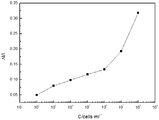
- Figure 7 shows the results of testing different concentrations of Salmonella by photoelectrochemical sensors based on organic electrochemical transistors.
- the present invention provides a photoelectrochemical biosensor and a method for preparing the same, and the present invention will be further described in detail below in order to make the objects, technical solutions and effects of the present invention more clear and clear. It is understood that the specific embodiments described herein are merely illustrative of the invention and are not intended to limit the invention.
- the invention provides a photoelectrochemical biosensor for detecting biomolecules, as shown in FIG. 1 and FIG. 2, comprising: an electrolytic cell 1, an electrolyte 2 disposed in the electrolytic cell 1, and being disposed in the electrolysis
- the photoelectric active semiconductor material is an organic semiconductor material, an inorganic semiconductor material or a combination of the two; for example, CdS, TiO 2 .
- the substrate is made of glass, a polymer flexible material such as PET or a silicon wafer.
- the source electrode, the drain electrode and the gate electrode are made of a metal material, a metal oxide semiconductor material, or an alloy material; for example, Au, Ag, Pt, Cu, ITO, or the like.
- the organic semiconductor thin film layer is composed of poly(3,4-ethylenedioxythiophene)-polystyrenesulfonic acid (PEDOT:PSS), polypyrrole, polythiophene, polyaniline, polyfluorene At least one of two or more copolymers of azole or poly(3,4-ethylenedioxythiophene)-polystyrenesulfonic acid, polypyrrole, polythiophene, polyaniline, and polycarbazole.
- PEDOT:PSS poly(3,4-ethylenedioxythiophene)-polystyrenesulfonic acid
- the source electrode and the drain electrode have a thickness of 50-500 nm.
- the organic semiconductor thin film layer has a thickness of 10 to 300 nm.
- the source electrode, the drain electrode and the gate electrode are placed in an electrolytic cell containing an electrolyte for detection as an electron donor.
- the organic electrochemical transistor (OECT) of the present invention is an organic thin film transistor (OTFT)
- OECT organic thin film transistor
- One of the important ones is low cost, easy to prepare, low operating voltage ( ⁇ 1V), good biocompatibility, easy miniaturization, and can be made into flexible devices. Since OECT has both sensing and signal amplification functions, it has very high sensitivity and low detection limit in biomolecule detection. At the same time, OECT can be fabricated into small-sized devices, which contributes to the miniaturization and integration of the sensor.
- the invention perfectly combines two biological detection technologies of OECT and PEC, and develops a novel biosensing technology of photoelectrochemistry based on organic electrochemical transistors. Because this technology combines the advantages of OECT and PEC, it has higher sensitivity and lower detection limit, and the device can be miniaturized and fabricated array detection system, which is expected to be widely used in biosensing.
- the probe ssDNA single-stranded DNA
- the antibody can be further immobilized on the surface of the gate electrode modified by the photoelectrically active semiconductor material, and the photoelectrochemical DNA sensor and the photoelectric device can be respectively prepared.
- Chemical immunosensors in order to achieve the purpose of measuring the concentration of bacteria such as ssDNA and Salmonella.
- the embodiment of the invention further provides a preparation method of the photoelectrochemical biosensor as described above, comprising the steps of:
- the source electrode and the drain electrode are prepared by one of vacuum thermal evaporation, magnetron sputtering or vapor deposition.
- the method for preparing the organic semiconductor thin film layer is spin coating or inkjet printing; the annealing temperature is 100-250 ° C, the annealing atmosphere is nitrogen, and the time is 20-60 min.
- the invention combines an organic electrochemical transistor (OECT) and a photoelectrochemical (PEC) bioanalytical method to modify a gate electrode in an OECT with a photoelectric active material, and causes a change of photocurrent on the gate electrode when the object to be tested is irradiated under illumination conditions.
- OECT organic electrochemical transistor
- PEC photoelectrochemical
- the senor has the advantages of simple structure, easy miniaturization, flexible device fabrication, low operating voltage ( ⁇ 1V) and the like.
- the new sensing technology has been successfully applied to DNA detection and immunosensing, and it has broad application prospects in various sensing fields such as enzyme biosensing and cell sensing.
- the gate electrode is an ITO electrode assembled with cadmium sulfide quantum dots (CdS QDs).
- CdS QDs cadmium sulfide quantum dots
- the electrons in the valence band of CdS will transition to the conduction band. Forming electron-hole pairs.
- the electron donor in the solution supplies electrons to the holes in the valence band, which forms a photocurrent. This current generation reduces the potential at the electrolyte/gate electrode interface, thereby increasing the effective gate voltage applied to the OECT device.
- the channel current of OECT is as shown in the following equation:
- V p qp 0 t/c i
- q represents the electron charge
- ⁇ represents the hole mobility
- p o represents the initial hole density in the organic semiconductor layer
- W and L represent the width and length of the device channel, respectively
- t represents the thickness of the organic semiconductor film
- C i represents The effective gate capacitance of the OECT device
- V P represents the pinch-off voltage
- V offset represents the compensation voltage
- the compensation voltage is related to the voltage drop at the interface between the gate-electrolyte and the electrolyte-channel.
- the channel current I ds of the organic electrochemical transistor is regulated by the gate voltage V G , it can be seen from the above equation that the channel current I ds decreases as the effective gate voltage increases.
- the step size formed by the "off-on" illumination in Fig. 3 indirectly reflects the magnitude of the photocurrent generated on the gate electrode, and the signal is amplified, so that when the magnitude of the photocurrent generated on the gate electrode changes.
- the size of the step formed by the illumination "off-on" in the I ds- T curve will also change, and the purpose of detection can be achieved by comparing the size of the step change before and after DNA hybridization.
- the present invention also designs a system based on the exciton-plasma effect between cadmium sulfide quantum dots (CdS QDs) and gold nanoparticles (Au NPs) to further enhance the sensitivity of the sensor due to the fluorescence of CdS QDs.
- CdS QDs cadmium sulfide quantum dots
- Au NPs gold nanoparticles
- the UV absorption spectra of the spectra and Au NPs overlap.
- the fluorescence of CdS QDs under illumination can excite the surface plasmon resonance of Au NPs. The interaction between them changes the exciton state in CdS QDs and causes the photocurrent to decrease.
- the Au NPs are modified on the target ssDNA (single-stranded DNA), and the probe ssDNA is attached to the gate electrode, which leads to a decrease in photocurrent after hybridization, and the illumination is off-on on the I ds -T curve.
- the reduction of the steps, the effect of photocurrent quenching caused by different concentrations of target ssDNA is different to achieve the effect of detecting different concentrations of DNA wherein Figure 4 is the I ds -T (channel) before and after the hybridization of the target ssDNA at a concentration of 10 -13 M
- the current-time curve, the DNA sensor has extremely high sensitivity and the detection limit can reach below 10 -13 M.
- the cleaned glass is adhered to the patterned mask, and the metal electrode is deposited by thermal evaporation to deposit 10 nm respectively. Cr and 100 nm of Au to obtain an Au/Cr/glass electrode, on which a layer of poly(3,4-ethylenedioxythiophene)-polystyrenesulfonic acid doped with dimethyl sulfoxide (DMSO) was spin-coated.
- DMSO dimethyl sulfoxide
- PEDOT:PSS the place where the PEDOT:PSS film is not required to be covered is wiped clean; it is annealed at 180 ° C for 30 min in a nitrogen atmosphere to make the PEDOT:PSS film adhere more firmly to the electrode surface and finally obtain the OECT device.
- Au NPs were carried out by the common NaBH 4 reduction of HAuCl 4 ; 0.6 mL of 0.1 M ice water prepared NaBH 4 was added to a stirred 20 mL 2.5 ⁇ 10 4 M HAuCl 4 solution; The solution quickly turned orange red to represent the formation of Au NPs. The solution was stirred in an ice water bath for 10 min, then stirred at room temperature for 3 h. During this process, the color of the solution gradually changed to wine red; after the stirring, gold glue The solution was stored in a refrigerator at 4 ° C until use.
- probe ssDNA on the surface of CdS QDs modified gate electrode by coupling reaction between NH 2 group on probe ssDNA and COOH group on CdS QDs; immersing CdS QDs modified electrode into 20mg /ml EDC (1-(3-dimethylaminopropyl)-3-ethylcarbodiimide hydrochloride) and 10 mg/ml NHS (N-hydroxysuccinimide) in 1 h, then carefully with water Rinse, 25 ⁇ L of probe ssDNA (1 ⁇ M) was dropped on the electrode surface and incubated at 4 ° C overnight, and carefully rinsed with 10 mM PBS to remove unfixed ssDNA; then, the electrode was blocked with 1 mM MEA (ethanolamine) at 4 ° C for 2 h. After careful washing with 10 mM PBS (phosphate buffer), the I ds -T curve was measured under illumination.
- EDC 1-(3-dimethylaminopropyl)-3
- Hybridization between target ssDNA and probe ssDNA 25 ⁇ L of different concentrations of Au NPs labeled target DNA were dropped on the surface of the probe ssDNA-modified gate electrode, and incubated at 37 ° C for 1 h at a concentration of 20 mM MgCl 2 .
- the unhybridized target ssDNA was removed by washing with 10 mM PBS, and then the I ds -T curve was measured under illumination.
- the photo-current change on the gate electrode is also measured by measuring the I ds -T curve of the device, and the antibody is attached to the gate electrode.
- the gate electrode is caused by the steric hindrance effect of Salmonella.
- the photocurrent decreases, and the decrease in photocurrent caused by different concentrations of Salmonella is different, so that different concentrations of Salmonella can be detected.
- Figure 5 is a graph showing changes in electrical signals before and after the binding of Salmonella to antibodies at a concentration of 10 8 cells/ml.
- Figure 6 shows the results of testing different concentrations of Salmonella using conventional photoelectrochemical analysis methods with a detection limit of 10 3 cells/ml.
- Figure 7 shows the results of a photoelectrochemical sensor based on an organic electrochemical transistor for testing different concentrations of Salmonella with a detection limit of 10 2 cells/ml. It can be seen that the sensitivity of the new sensing technology is higher than that of the conventional photoelectrochemical sensing technology.
- the cleaned glass is adhered to the patterned mask, and the metal electrode is deposited by thermal evaporation to deposit 10 nm respectively. Cr and 100 nm of Au to obtain an Au/Cr/glass electrode, and a layer of dimethyl sulfoxide (DMSO) was spin-coated on the electrode.
- DMSO dimethyl sulfoxide
- PEDOT:PSS Poly(3,4-ethylenedioxythiophene)-polystyrenesulfonic acid
- the gate electrode modified with antibody was soaked in 1 ml of different concentrations of Salmonella solution (10 mM PBS solution) for 1 h at room temperature for full binding, then carefully rinsed with 10 mM PBS to remove unbound Salmonella , under the illumination, measure the I ds -T curve.
- the invention combines photoelectrochemical (PEC) biosensing technology with organic electrochemical transistor (OECT) for the first time. Since OECT has both sensing and signal amplification, it can amplify the weak current signal change on the gate electrode.
- This sensor has extremely high sensitivity.
- the device of the invention has various preparation methods, simple structure and small device size, and all components can be integrated into a small substrate, which is easy to integrate, miniaturize and array, and is suitable for mass production; the sensor has low operating voltage ( ⁇ 1V).
- the organic semiconductor thin film layer and the semiconductor material assembled on the gate electrode can be selected from biocompatible materials to provide good stability to the sensor; in addition, the present invention has universal applicability in the field of biological detection, and can be applied to DNA. In addition to sensors and immunosensors, it can be widely applied to various biosensing methods such as enzyme biosensing and cell sensing.
- organic semiconductor thin film layer in the organic electrochemical transistor of the present invention can also be replaced with other inorganic semiconductor thin film materials such as graphene.
- the invention modifies the photoelectric active material on the OECT gate electrode, causes the electrolyte/gate electrode interface potential change under illumination to achieve the purpose of biomolecule detection, and modifies the photoelectric active material on the organic semiconductor thin film layer in the organic electrochemical transistor under illumination
- the change in the electrolyte/channel interface potential can also achieve the purpose of sensing.
- the photoelectrochemical biosensor of the present invention has extremely high sensitivity.
- the structure is simple and the device size is small, which solves the problem that the existing photoelectrochemical biosensor is not easy to be miniaturized.
- the photoelectrochemical biosensor of the invention has universal applicability in the field of biological detection, and can be widely applied to biological sensors such as enzyme biosensing and cell sensing, in addition to being applied to DNA sensors and immunosensors.
Landscapes
- Health & Medical Sciences (AREA)
- Life Sciences & Earth Sciences (AREA)
- Chemical & Material Sciences (AREA)
- Molecular Biology (AREA)
- Physics & Mathematics (AREA)
- Chemical Kinetics & Catalysis (AREA)
- General Health & Medical Sciences (AREA)
- Engineering & Computer Science (AREA)
- Spectroscopy & Molecular Physics (AREA)
- Electrochemistry (AREA)
- Analytical Chemistry (AREA)
- Biochemistry (AREA)
- Microelectronics & Electronic Packaging (AREA)
- General Physics & Mathematics (AREA)
- Immunology (AREA)
- Pathology (AREA)
- Investigating Or Analyzing Materials By The Use Of Electric Means (AREA)
- Apparatus Associated With Microorganisms And Enzymes (AREA)
- Thin Film Transistor (AREA)
Abstract
一种光电化学生物传感器及其制备方法,光电化学生物传感器包括:电解池(1),设置在电解池(1)内的电解液(2),设置在电解池(1)内的有机电化学晶体管(9),及设置在电解池(1)内的栅电极(3);有机电化学晶体管(9)包括:衬底(5),设置在衬底(5)之上的源电极(7)和漏电极(8),及涂覆在衬底(5)之上连接源电极(7)和漏电极(8)的有机半导体薄膜层(6);栅电极(3)上修饰有光电活性半导体材料(4)作为传感器的敏感功能层。光电化学生物传感器具有极高的灵敏度,且结构简单、器件尺寸小,解决了光电化学生物传感器不易微型化的问题。光电化学生物传感器在生物检测领域具有普适性,除可以应用于DNA传感器和免疫传感器外,在酶生物传感、细胞传感等生物传感方面也都可以广泛适用。
Description
本发明涉及生物传感技术领域,尤其涉及一种光电化学生物传感器及其制备方法。
光电化学(PEC)生物传感技术是在电化学分析方法的基础上发展起来的一种生物传感技术,由于其灵敏度高、价格低廉及设备简单等优点,已被广泛应用于酶生物传感、DNA传感、免疫传感、及细胞传感等各种生物传感。PEC的检测原理是基于在光照下识别元件和目标分子之间的生物识别作用而产生相应电信号的改变。目前,对于PEC生物传感器中信号的检测主要通过电化学工作站,建立一个由工作电极、参比电极、及对电极组成的三电极测试系统来检测光电流的大小。该系统虽然结构简单,但不利于器件化,也为该传感器的微型化带来不便。
因此,现有技术还有待于改进和发展。
发明内容
鉴于上述现有技术的不足,本发明的目的在于提供一种光电化学生物传感器及其制备方法,从而进一步提高光电化学生物传感器的灵敏度及解决现有的光电化学生物传感器不易微型化的问题。
本发明的技术方案如下:
一种光电化学生物传感器,包括:电解池,设置在所述电解池内的电解液,设置在所述电解池内的有机电化学晶体管,及设置在所述电解池内的栅电极;所述有机电化学晶体管包括:衬底,设置在所述衬底之上的源电极和漏电极,及涂覆在衬底之上连接源电极和漏电极的有机半导体薄膜层;所述栅电极上修饰有光电活性半导体材料作为传感器的敏感功能层。
所述的光电化学生物传感器,其中,所述光电活性半导体材料为有机半导体材料、无机半导体材料或二者的组合。
所述的光电化学生物传感器,其中,所述衬底是由玻璃、聚合物柔性材料或硅片制成。
所述的光电化学生物传感器,其中,所述源电极、漏电极及栅电极是由金属材料、金属氧化物半导体材料、合金材料构成。
所述的光电化学生物传感器,其中,所述有机半导体薄膜层由聚(3,4-乙烯二氧噻吩)-聚苯乙烯磺酸、聚吡咯、聚噻吩、聚苯胺、聚咔唑或者聚(3,4-乙烯二氧噻吩)-聚苯乙烯磺酸、聚吡咯、聚噻吩、聚苯胺、聚咔唑的两种或两种以上的共聚物中的至少一种构成。
所述的光电化学生物传感器,其中,所述源电极和漏电极的厚度为50-500nm。
所述的光电化学生物传感器,其中,所述有机半导体薄膜层的厚度为10-300nm。
一种如以上任一项所述的光电化学生物传感器的制备方法,包括步骤:
A、彻底清洗衬底并干燥,在衬底上制备源电极和漏电极,在源电极和漏电极之间制备有机半导体薄膜层,得到有机电化学晶体管;
B、彻底清洗栅电极并干燥,在栅电极上修饰光电活性半导体材料作为传感器的敏感功能层,得到修饰后的栅电极;
C、将有机电化学晶体管和修饰后的栅电极放置于装有电解液的电解池中,制得所述光电化学生物传感器。
所述的光电化学生物传感器的制备方法,其中,所述步骤A中,所述的源电极和漏电极是通过真空热蒸镀、磁控溅射或气相沉积中的一种方法制备。
所述的光电化学生物传感器的制备方法,其中,所述步骤A中,制备有机半导体薄膜层的方法为旋涂或喷墨印刷;退火温度为100-250℃,退火氛围为氮气,时间为20-60min。
有益效果:本发明首次将光电化学生物传感技术与有机电化学晶体管相结合,由于有机电化学晶体管兼具传感和信号放大的作用,可对栅电极上微弱的电流信号变化进行放大,因此该传感器具有极高的灵敏度。本发明结构简单、器件尺寸小,所有部件都可以集成到一个微小衬底上,解决了现有的光电化学生物传感器不易微型化的问题。本发明在生物检测领域具有普适性,除可以应用于DNA传感器和免疫传感器外,在酶生物传感、细胞传感等各种生物传感方面也都可以广泛适用。
图1是本发明光电化学生物传感器的整体结构示意图。
图2是本发明所述有机电化学晶体管的结构示意图。
图3为光照“关-开”下栅电极修饰有CdS QDs的器件的Ids-T曲线。
图4为DNA杂化前后(目标DNA浓度为10-13M)所测的Ids-T曲线(a为CdS QDs修饰的栅电极的Ids-T曲线,b为探针ssDNA在CdS QDs修饰的栅电极的Ids-T曲线,c为目标ssDNA和探针ssDNA杂化后的Ids-T曲线)。
图5为沙门氏菌(沙门氏菌浓度为108cells/ml)与抗体结合前后所测的Ids-T曲线(a为CdS QDs修饰的栅电极的Ids-T曲线,b为固定抗体在CdS QDs修饰的栅电极上的Ids-T曲线,c为沙门氏菌与抗体结合后的Ids-T曲线)。
图6为采用光电化学分析方法测试不同浓度沙门氏菌的结果。
图7为基于有机电化学晶体管的光电化学传感器测试不同浓度沙门氏菌的结果。
本发明提供一种光电化学生物传感器及其制备方法,为使本发明的目的、技术方案及效果更加清楚、明确,以下对本发明进一步详细说明。应当理解,此处所描述的具体实施例仅仅用以解释本发明,并不用于限定本发明。
本发明提供一种光电化学生物传感器,用于生物分子的检测,如图1、图2所示,包括:电解池1,设置在所述电解池1内的电解液2,设置在所述电解池1内的有机电化学晶体管9,及设置在所述电
解池内的栅电极3;所述有机电化学晶体管9包括:衬底5,设置在所述衬底5之上的源电极7和漏电极8,及涂覆在衬底5之上连接源电极7和漏电极8的有机半导体薄膜层6;所述栅电极3上修饰有光电活性半导体材料4作为传感器的敏感功能层。
进一步的,本发明实施例中,所述光电活性半导体材料为有机半导体材料、无机半导体材料或二者的组合;例如CdS、TiO2。
进一步的,本发明实施例中,所述衬底是由玻璃、聚合物柔性材料(例如PET)或硅片制成。
进一步的,本发明实施例中,所述源电极、漏电极及栅电极是由金属材料、金属氧化物半导体材料、合金材料构成;例如Au、Ag、Pt、Cu、ITO等。
进一步的,本发明实施例中,所述有机半导体薄膜层由聚(3,4-乙烯二氧噻吩)-聚苯乙烯磺酸(PEDOT:PSS)、聚吡咯、聚噻吩、聚苯胺、聚咔唑或者聚(3,4-乙烯二氧噻吩)-聚苯乙烯磺酸、聚吡咯、聚噻吩、聚苯胺、聚咔唑的两种或两种以上的共聚物中的至少一种构成。
进一步的,本发明实施例中,所述源电极和漏电极的厚度为50-500nm。
进一步的,本发明实施例中,所述有机半导体薄膜层的厚度为10-300nm。
进一步的,本发明实施例中,将源电极、漏电极和栅电极放置于装有电解液的电解池中进行检测,所述电解液用于作为电子给体。
本发明所述有机电化学晶体管(OECT)为有机薄膜晶体管(OTFT)
中的其中重要一类,其具有成本低、容易制备、工作电压低(<1V)、生物兼容性好、易微型化、可制成柔性器件等诸多优点。由于OECT同时具有传感和信号放大的功能,因此在生物分子检测中具有非常高的灵敏度和低的检测极限。与此同时,OECT可制备成小尺寸器件,有利于传感器的微型化和可集成性。
本发明将OECT和PEC两种生物检测技术完美结合在一起,开发出一种基于有机电化学晶体管的光电化学新型生物传感技术。由于该技术结合了OECT和PEC的各自优势,因此具有更高的灵敏度和更低的检测极限,且器件可微型化并制作阵列检测系统,有望在生物传感领域得到广泛的应用。
在本发明所述光电化学生物传感器的基础上,可以通过进一步在光电活性半导体材料修饰的栅电极表面上固定探针ssDNA(单链DNA)、抗体等,分别对应制得光电化学DNA传感器和光电化学免疫传感器,从而达到对应检测目标ssDNA和沙门氏菌等细菌浓度的目的。
本发明实施例还提供了一种如以上所述的光电化学生物传感器的制备方法,包括步骤:
S100、彻底清洗衬底并干燥,在衬底上制备源电极和漏电极,在源电极和漏电极之间制备有机半导体薄膜层,得到有机电化学晶体管;
S200、彻底清洗栅电极并干燥,在栅电极上修饰光电活性半导体材料作为传感器的敏感功能层,得到修饰后的栅电极;
S300、将有机电化学晶体管和修饰后的栅电极放置于装有电解液
的电解池中,制得所述光电化学生物传感器。
优选地,所述步骤S100中,所述的源电极和漏电极是通过真空热蒸镀、磁控溅射或气相沉积中的一种方法制备。
优选地,所述步骤S100中,制备有机半导体薄膜层的方法为旋涂或喷墨印刷;退火温度为100-250℃,退火氛围为氮气,时间为20-60min。
本发明将有机电化学晶体管(OECT)和光电化学(PEC)生物分析方法相结合,以光电活性材料修饰OECT中的栅电极,在光照条件下,当待测物引起栅电极上光电流的变化时,会进一步引起OECT相关电学参数(界面电势、有效栅电压、沟道电流等)的变化,最终通过测量OECT沟道电流的变化来实现对生物分子的检测。由于OECT兼具传感和信号放大的作用,可对栅电极上微弱的电流信号变化进行放大,因此该传感器具有极高的灵敏度。此外,该传感器还有结构简单、易微型化、可制成柔性器件、工作电压低(<1V)等诸多优点。该新型传感技术目前已成功应用于DNA检测和免疫传感,其在酶生物传感和细胞传感等各种传感领域将具有广泛的应用前景。
下面以具体实施例对本发明作详细说明:
实施例1基于有机电化学晶体管的光电化学DNA传感器
原理:栅电极选用组装有硫化镉量子点(CdS QDs)的ITO电极,在光照条件下,当光的能量大于CdS中电子跃迁所需的能量时,CdS中价带的电子会跃迁至导带,形成电子-空穴对。当导带中的电子注入电极,溶液中电子给体提供电子给价带中的空穴,会形成光电流,
该电流的产生会降低电解质/栅电极界面的电位,从而增加施加在OECT器件上的有效栅电压。OECT的沟道电流如以下方程所示:

Vp=qp0t/ci

其中q代表电子电量,μ代表空穴迁移率,po代表有机半导体层中的初始空穴密度,W和L分别代表器件沟道的宽度和长度,t代表有机半导体膜的厚度,Ci代表OECT器件的有效栅电容,VP代表夹断电压, 代表有效栅电压,Voffset代表补偿电压,补偿电压与栅极-电解液、电解液-沟道这两个界面的电压降有关系。
由于有机电化学晶体管的沟道电流Ids受到栅电压VG的调控,由以上方程可以看出,当有效栅电压增大时沟道电流Ids会减小。图3中光照“关-开”(off-on)形成的台阶大小间接反映了栅电极上产生光电流的大小,并且对该信号进行了放大,因此当栅电极上产生的光电流大小改变时,Ids-T曲线中光照“关-开”所形成的台阶大小也会随之改变,通过比较DNA杂化前后台阶变化的大小可以达到检测的目的。
在该实例中,本发明还设计了基于硫化镉量子点(CdS QDs)和金纳米颗粒(Au NPs)之间的激子-等离子体效应的体系来进一步提升传感器的灵敏度,由于CdS QDs的荧光光谱和Au NPs的紫外吸收光谱重叠,光照条件下CdS QDs的荧光可以激发Au NPs发生表面等离子体共振,它们间的相互作用会改变CdS QDs内的激子状态,引起光电流的降低。因此,在目标ssDNA(单链DNA)上修饰Au NPs,
在栅电极上连接探针ssDNA,其发生杂化后会导致光电流的降低,在Ids-T曲线上表现为光照“关-开”台阶的减小,根据不同浓度目标ssDNA引起光电流猝灭的效果不同达到检测不同浓度DNA的效果,其中图4为浓度为10-13M目标ssDNA杂化前后的Ids-T(沟道电流-时间)曲线,该DNA传感器具有极高的灵敏度,检测极限可达10-13M以下浓度。
基于有机电化学晶体管的光电化学DNA传感器的制备过程
1.制作有机电化学晶体管(OECT)的源电极、漏电极及有机半导体薄膜层:将清洗好的玻璃贴紧在设计好图案的掩模板上,通过热蒸镀沉积金属电极,分别沉积10nm的Cr和100nm的Au以得到Au/Cr/玻璃电极,在该电极上旋涂一层掺有二甲基亚砜(DMSO)的聚(3,4-乙烯二氧噻吩)-聚苯乙烯磺酸(PEDOT:PSS),将不需要覆盖PEDOT:PSS膜的地方擦除干净;在氮气氛围180℃退火30min,使PEDOT:PSS膜更加牢固的附着在电极表面并最终得到了OECT器件。
2.TGA(巯基乙酸)修饰的CdS QDs的合成:在三口烧瓶中加入50mL 0.01M CdCl2溶液,搅拌,通入氮气,升温至40℃后加入250μL TGA,反应30min;在此期间,使用1M的NaOH溶液调节混合液的pH到11;然后,加入5.0mL 0.1M Na2S溶液,氮气氛围下110℃加热,回流4h,用水(体积比1:1)稀释后,保存于4℃冰箱待用。
3.Au NPs的合成:Au NPs通过常见的NaBH4还原HAuCl4的方法来进行;0.6mL 0.1M冰水配制的NaBH4加入到不停搅拌的20mL2.5×104M HAuCl4溶液中;溶液迅速变为橘红色代表Au NPs的形成,
该溶液继续在冰水浴中搅拌10min,随后在常温条件下搅拌3h,在此过程中,溶液颜色会逐渐变为酒红色;搅拌结束后,金胶溶液保存于4℃冰箱待用。
4.CdS QDs修饰的栅电极的制备:将洗净干燥后的ITO电极依次浸入2%PDDA(聚合物电解质,0.5M NaCl溶液配制)和CdS QDs溶液中各10min,每次浸泡完用水清洗,该过程重复3次,得到所需的多层膜修饰电极,CdS QDs干燥稳定后在光照下测量Ids-T曲线。
5.探针ssDNA在CdS QDs修饰的栅电极表面的固定:通过探针ssDNA上的NH2基团和CdS QDs上的COOH基团之间的偶联反应进行;将CdS QDs修饰的电极浸入20mg/ml EDC(1-(3-二甲氨基丙基)-3-乙基碳二亚胺盐酸盐)和10mg/ml NHS(N-羟基琥珀酰亚胺)的溶液中1h,随后用水小心冲洗,将25μL探针ssDNA(1μM)滴在电极表面并4℃孵化过夜后,使用10mM PBS小心冲洗,以便去除未固定的ssDNA;然后,使用1mM MEA(乙醇胺)于4℃封闭电极2h,再用10mM PBS(磷酸盐缓冲液)小心冲洗后,在光照下,测量Ids-T曲线。
6.Au NPs对目标ssDNA的标记:首先使用10mM TCEP活化目标DNA上的巯基,还原双硫键;在50μL 10μM的活化过的目标DNA中加入1ml所制备的Au NPs溶液,摇床震荡过夜,期间加入0.5M NaCl溶液,离心收集后4℃保存备用,不同浓度的Au NPs修饰的目标DNA通过加入对应体积的10mM PBS进行稀释。
7.目标ssDNA和探针ssDNA之间的杂化:25μL的不同浓度Au
NPs标记的目标DNA滴在探针ssDNA修饰的栅电极表面,在浓度为20mM的MgCl2条件下37℃孵化1h,之后用10mM PBS冲洗,去除未杂化的目标ssDNA,然后,在光照下,测量Ids-T曲线。
在该实例中,CdS QDs修饰、连接探针ssDNA以及和目标ssDNA杂化后的栅电极的Ids-T曲线在0.1M AA(抗坏血酸)溶液(0.1M PBS溶液配制)中测量,VG=0V,VDS=0.1V,激发波长为420nm。
实施例2基于有机电化学晶体管的光电化学免疫传感器
原理:同样是通过测量器件的Ids-T曲线来反应栅电极上光电流的变化,在栅电极上连接抗体,当抗体与沙门氏菌发生特异性结合时,由于沙门氏菌的位阻效应会使得栅电极光电流下降,并且不同浓度沙门氏菌引起光电流的下降值不同,据此可以对不同浓度的沙门氏菌进行检测。
图5为浓度为108cells/ml沙门氏菌与抗体结合前后的电学信号变化图。图6为采用传统的光电化学分析方法测试不同浓度沙门氏菌的结果,检测极限为103cells/ml。图7为基于有机电化学晶体管的光电化学传感器测试不同浓度沙门氏菌的结果,检测极限为102cells/ml。由此可见,该新型传感技术的灵敏度要高于传统的光电化学传感技术。
基于有机电化学晶体管的光电化学免疫传感器的制备过程
1.制作有机电化学晶体管(OECT)的源电极、漏电极及有机半导体薄膜层:将清洗好的玻璃贴紧在设计好图案的掩模板上,通过热蒸镀沉积金属电极,分别沉积10nm的Cr和100nm的Au以得到Au/Cr/玻璃电极,在该电极上旋涂一层掺有二甲基亚砜(DMSO)的
聚(3,4-乙烯二氧噻吩)-聚苯乙烯磺酸(PEDOT:PSS),将不需要覆盖PEDOT:PSS膜的地方擦除干净;在氮气氛围180℃退火1h,使PEDOT:PSS膜更加牢固的附着在电极表面并最终得到了OECT器件。
2.TGA修饰的CdS QDs的合成:在三口烧瓶中加入50mL 0.01M CdCl2溶液,搅拌,通入氮气,升温至40℃后加入250μL TGA,反应30min;在此期间,使用1M的NaOH溶液调节混合液的pH到11;然后,加入5.0mL 0.1M Na2S溶液,氮氛下110℃加热,回流4h,用水(体积比1:1)稀释后,保存于4℃冰箱待用。
3.CdS QDs修饰的栅电极的制备:将洗净干燥后的ITO电极依次浸入2%PDDA(0.5M NaCl溶液配制)和CdS QDs溶液中各10min,每次浸泡完用水清洗,该过程重复3次,得到所需的多层膜修饰电极,在光照下,测量Ids-T曲线。
4.抗体在CdS QDs修饰的栅电极表面的固定:通过抗体上的NH2基团和CdS QDs上的COOH基团之间的偶联反应进行;将CdS QDs修饰的电极浸入20mg/ml EDC(1-(3-二甲氨基丙基)-3-乙基碳二亚胺盐酸盐)和10mg/ml NHS(N-羟基琥珀酰亚胺)的溶液中1h,随后用水小心冲洗,将25μL抗体(2mg/ml)滴在电极表面并4℃孵化过夜后,使用10mM PBS小心冲洗,以便去除未固定的抗体;然后,使用1mM MEA于4℃封闭电极2h,再用10mM PBS小心冲洗后,在光照下,测量Ids-T曲线。
5.沙门氏菌与抗体的结合:修饰有抗体的栅电极在1ml在不同浓度的沙门氏菌溶液中(10mM PBS溶液配制)室温下浸泡1h以便其
充分结合,然后用10mM PBS小心冲洗,除去未结合的沙门氏菌,在光照下,测量Ids-T曲线。
在该实例中,CdS QDs修饰、连接抗体以及和沙门氏菌结合后的栅电极的Ids-T曲线在0.1M抗坏血酸(AA)溶液(0.1M PBS溶液配制)中测量,VG=0V,VDS=0.1V,激发波长为420nm。
本发明首次将光电化学(PEC)生物传感技术与有机电化学晶体管(OECT)相结合,由于OECT兼具传感和信号放大的作用,可对栅电极上微弱的电流信号变化进行放大,因此该传感器具有极高的灵敏度。本发明器件制备方法多样,结构简单、器件尺寸小,所有部件都可以集成到一个微小衬底上,易集成化、微型化、阵列化,适合大规模生产;该传感器工作电压低(<1V),有机半导体薄膜层和组装于栅电极上的半导体材料都可选用生物兼容性好的材料,为传感器提供良好的稳定性;此外,本发明在生物检测领域具有普适性,除可以应用于DNA传感器和免疫传感器外,在酶生物传感、细胞传感等各种生物传感方面也都可以广泛适用。
另外需要说明的是,本发明有机电化学晶体管中的有机半导体薄膜层也可换成其他无机半导体薄膜材料如石墨烯。本发明是在OECT栅电极上修饰光电活性材料,光照下引起电解质/栅电极界面电位变化来达到生物分子检测目的,而在有机电化学晶体管中的有机半导体薄膜层上修饰光电活性材料,光照下引起电解质/沟道界面电位变化亦可同样达到传感检测目的。
综上所述,本发明所述光电化学生物传感器具有极高的灵敏度,
且结构简单、器件尺寸小,解决了现有的光电化学生物传感器不易微型化的问题。本发明光电化学生物传感器在生物检测领域具有普适性,除可以应用于DNA传感器和免疫传感器外,在酶生物传感、细胞传感等生物传感方面也都可以广泛适用。
应当理解的是,本发明的应用不限于上述的举例,对本领域普通技术人员来说,可以根据上述说明加以改进或变换,所有这些改进和变换都应属于本发明所附权利要求的保护范围。
Claims (10)
- 一种光电化学生物传感器,其特征在于,包括:电解池,设置在所述电解池内的电解液,设置在所述电解池内的有机电化学晶体管,及设置在所述电解池内的栅电极;所述有机电化学晶体管包括:衬底,设置在所述衬底之上的源电极和漏电极,及涂覆在衬底之上连接源电极和漏电极的有机半导体薄膜层;所述栅电极上修饰有光电活性半导体材料作为传感器的敏感功能层。
- 根据权利要求1所述的光电化学生物传感器,其特征在于,所述光电活性半导体材料为有机半导体材料、无机半导体材料或二者的组合。
- 根据权利要求1所述的光电化学生物传感器,其特征在于,所述衬底是由玻璃、聚合物柔性材料或硅片制成。
- 根据权利要求1所述的光电化学生物传感器,其特征在于,所述源电极、漏电极及栅电极是由金属材料、金属氧化物半导体材料、合金材料构成。
- 根据权利要求1所述的光电化学生物传感器,其特征在于,所述有机半导体薄膜层由聚(3,4-乙烯二氧噻吩)-聚苯乙烯磺酸、聚吡咯、聚噻吩、聚苯胺、聚咔唑或者聚(3,4-乙烯二氧噻吩)-聚苯乙烯磺酸、聚吡咯、聚噻吩、聚苯胺、聚咔唑的两种或两种以上的共聚物中的至少一种构成。
- 根据权利要求1所述的光电化学生物传感器,其特征在于,所述源电极和漏电极的厚度为50-500nm。
- 根据权利要求1所述的光电化学生物传感器,其特征在于,所述有机半导体薄膜层的厚度为10-300nm。
- 一种如权利要求1-7任一项所述的光电化学生物传感器的制备方法,其特征在于,包括步骤:A、彻底清洗衬底并干燥,在衬底上制备源电极和漏电极,在源电极和漏电极之间制备有机半导体薄膜层,得到有机电化学晶体管;B、彻底清洗栅电极并干燥,在栅电极上修饰光电活性半导体材料作为传感器的敏感功能层,得到修饰后的栅电极;C、将有机电化学晶体管和修饰后的栅电极放置于装有电解液的电解池中,制得所述光电化学生物传感器。
- 根据权利要求8所述的光电化学生物传感器的制备方法,其特征在于,所述步骤A中,所述的源电极和漏电极是通过真空热蒸镀、磁控溅射或气相沉积中的一种方法制备。
- 根据权利要求8所述的光电化学生物传感器的制备方法,其特征在于,所述步骤A中,制备有机半导体薄膜层的方法为旋涂或喷墨印刷;退火温度为100-250℃,退火氛围为氮气,时间为20-60min。
Applications Claiming Priority (2)
| Application Number | Priority Date | Filing Date | Title |
|---|---|---|---|
| CN201611054180.7 | 2016-11-25 | ||
| CN201611054180.7A CN106770587B (zh) | 2016-11-25 | 2016-11-25 | 一种光电化学生物传感器及其制备方法 |
Publications (1)
| Publication Number | Publication Date |
|---|---|
| WO2018094779A1 true WO2018094779A1 (zh) | 2018-05-31 |
Family
ID=58912497
Family Applications (1)
| Application Number | Title | Priority Date | Filing Date |
|---|---|---|---|
| PCT/CN2016/109398 Ceased WO2018094779A1 (zh) | 2016-11-25 | 2016-12-12 | 一种光电化学生物传感器及其制备方法 |
Country Status (2)
| Country | Link |
|---|---|
| CN (1) | CN106770587B (zh) |
| WO (1) | WO2018094779A1 (zh) |
Cited By (12)
| Publication number | Priority date | Publication date | Assignee | Title |
|---|---|---|---|---|
| CN110702910A (zh) * | 2019-08-27 | 2020-01-17 | 东南大学 | 一种检测dna甲基化酶活性的光电化学免疫传感器及其制备方法和应用 |
| CN111796012A (zh) * | 2020-05-26 | 2020-10-20 | 南京邮电大学 | 一种基于高效稳定原位生长二氧化钛/纳米金光阳极的光电化学传感器制备方法 |
| CN112666237A (zh) * | 2020-11-23 | 2021-04-16 | 广州大学 | 基于硫化镉纳米颗粒/二氧化钛纳米线阵列复合材料的光电化学传感器的制备及其应用 |
| CN112710709A (zh) * | 2020-12-22 | 2021-04-27 | 武汉理工大学 | 用于目标dna检测的硫化镉量子点玻碳电极及其制备方法、电化学发光传感器系统与应用 |
| CN113036042A (zh) * | 2021-03-05 | 2021-06-25 | 天津大学 | 基于有机薄膜场效应晶体管的光电生物化学传感器及其制备方法和应用 |
| CN113333042A (zh) * | 2021-06-21 | 2021-09-03 | 太原理工大学 | 一种用于核酸检测的微流控芯片及其制作方法 |
| CN113702461A (zh) * | 2021-08-11 | 2021-11-26 | 常州大学 | 一种光电化学自供能传感器的制备方法及在检测林可霉素中的应用 |
| CN114019000A (zh) * | 2021-11-03 | 2022-02-08 | 北京师范大学 | 一种多信号响应薄膜电极、其制备方法、及其应用 |
| US20220065806A1 (en) * | 2020-09-03 | 2022-03-03 | Mcmaster University | Photoelectrochemical biosensor and methods of use thereof |
| CN114674894A (zh) * | 2022-03-18 | 2022-06-28 | 济南大学 | GQDs@ZIF-8作为信号猝灭器传感器的构建 |
| CN114927614A (zh) * | 2022-04-21 | 2022-08-19 | 西安交通大学 | 一种自供电的电化学传感器及其太阳能电池与加工方法 |
| CN116953041A (zh) * | 2023-06-16 | 2023-10-27 | 国科温州研究院(温州生物材料与工程研究所) | 一种高灵敏快响应的pH传感器及其工作方法 |
Families Citing this family (9)
| Publication number | Priority date | Publication date | Assignee | Title |
|---|---|---|---|---|
| CN106770566B (zh) * | 2016-11-25 | 2019-04-16 | 深圳大学 | 沙门氏菌传感器、制备方法及沙门氏菌浓度的检测方法 |
| WO2020127638A1 (en) * | 2018-12-19 | 2020-06-25 | Valotec | Organic electrochemical transistor having an improved conductive channel |
| US12292406B2 (en) * | 2019-08-03 | 2025-05-06 | King Abdullah University Of Science And Technology | Device for detecting analytes in a sample, and methods of use thereof |
| CN111551717B (zh) * | 2020-04-10 | 2023-04-07 | 深圳大学 | 一种基于有机光电化学晶体管的胃泌素释放肽前体传感器及其制备方法与应用 |
| CN113203785B (zh) * | 2021-03-26 | 2022-09-27 | 深圳大学 | 一种基于有机光电化学晶体管的Aβ寡聚体生物传感器及其制备方法与应用 |
| CN113025124B (zh) * | 2021-04-09 | 2022-10-21 | 深圳大学 | 一种有机半导体墨水及全喷墨打印有机电化学晶体管器件的方法 |
| CN114113271B (zh) * | 2021-10-20 | 2023-12-15 | 杭州富鼎检测有限公司 | 一种检测农药马拉硫磷的光电化学有机晶体管传感器的制备方法 |
| CN116500111B (zh) * | 2023-04-04 | 2026-02-10 | 深圳大学 | 一种用于检测单细胞内atp的探针型有机电化学晶体管传感器及其制备方法、检测方法 |
| CN120044097B (zh) * | 2025-02-20 | 2026-07-17 | 中电科芯片技术(集团)有限公司 | 一种高性能有机电化学晶体管阵列敏感元件及传感器 |
Citations (6)
| Publication number | Priority date | Publication date | Assignee | Title |
|---|---|---|---|---|
| CN102507659A (zh) * | 2011-11-28 | 2012-06-20 | 电子科技大学 | 基于有机薄膜晶体管的甲醛气体传感器及其制备方法 |
| CN102735734A (zh) * | 2011-03-29 | 2012-10-17 | 香港理工大学 | 一种非介入式葡萄糖传感器 |
| CN103558270A (zh) * | 2013-10-18 | 2014-02-05 | 海南大学 | 基于有机电化学晶体管的海洋微生物附着传感器及制备方法 |
| US8895340B1 (en) * | 2013-09-10 | 2014-11-25 | Georgetown University | Biosensor and system and process for forming |
| CN104950023A (zh) * | 2014-03-28 | 2015-09-30 | Nlt科技股份有限公司 | Tft离子传感器、使用该tft离子传感器的tft离子传感器装置 |
| CN105136893A (zh) * | 2015-06-24 | 2015-12-09 | 中国科学院宁波材料技术与工程研究所 | 一种薄膜晶体管生物传感器及其制备方法 |
Family Cites Families (6)
| Publication number | Priority date | Publication date | Assignee | Title |
|---|---|---|---|---|
| CN1516292A (zh) * | 2003-01-08 | 2004-07-28 | 威凯科技股份有限公司 | 光控晶体管的制造方法及其结构 |
| GB2437768A (en) * | 2006-05-03 | 2007-11-07 | Seiko Epson Corp | Photosensing TFT |
| RU2011118354A (ru) * | 2008-10-08 | 2012-11-20 | Массачусетс Инститьют Оф Текнолоджи (Us) | Каталитические материалы, фотоаноды и фотоэлектрические ячейки для электролиза воды и других электрохимических технологий |
| CN101776637B (zh) * | 2009-01-13 | 2013-11-06 | 国家纳米科学中心 | 一种光电化学生物传感器及其制备方法 |
| CN105679937A (zh) * | 2016-01-08 | 2016-06-15 | 中国计量学院 | 一种双栅结构的光敏有机场效应晶体管及其制备方法 |
| CN106018514B (zh) * | 2016-07-05 | 2019-04-05 | 济南大学 | 一种基于铜掺杂纳米光电材料的光电化学己烯雌酚传感器的制备方法 |
-
2016
- 2016-11-25 CN CN201611054180.7A patent/CN106770587B/zh active Active
- 2016-12-12 WO PCT/CN2016/109398 patent/WO2018094779A1/zh not_active Ceased
Patent Citations (6)
| Publication number | Priority date | Publication date | Assignee | Title |
|---|---|---|---|---|
| CN102735734A (zh) * | 2011-03-29 | 2012-10-17 | 香港理工大学 | 一种非介入式葡萄糖传感器 |
| CN102507659A (zh) * | 2011-11-28 | 2012-06-20 | 电子科技大学 | 基于有机薄膜晶体管的甲醛气体传感器及其制备方法 |
| US8895340B1 (en) * | 2013-09-10 | 2014-11-25 | Georgetown University | Biosensor and system and process for forming |
| CN103558270A (zh) * | 2013-10-18 | 2014-02-05 | 海南大学 | 基于有机电化学晶体管的海洋微生物附着传感器及制备方法 |
| CN104950023A (zh) * | 2014-03-28 | 2015-09-30 | Nlt科技股份有限公司 | Tft离子传感器、使用该tft离子传感器的tft离子传感器装置 |
| CN105136893A (zh) * | 2015-06-24 | 2015-12-09 | 中国科学院宁波材料技术与工程研究所 | 一种薄膜晶体管生物传感器及其制备方法 |
Cited By (18)
| Publication number | Priority date | Publication date | Assignee | Title |
|---|---|---|---|---|
| CN110702910A (zh) * | 2019-08-27 | 2020-01-17 | 东南大学 | 一种检测dna甲基化酶活性的光电化学免疫传感器及其制备方法和应用 |
| CN111796012A (zh) * | 2020-05-26 | 2020-10-20 | 南京邮电大学 | 一种基于高效稳定原位生长二氧化钛/纳米金光阳极的光电化学传感器制备方法 |
| US20220065806A1 (en) * | 2020-09-03 | 2022-03-03 | Mcmaster University | Photoelectrochemical biosensor and methods of use thereof |
| US11874247B2 (en) * | 2020-09-03 | 2024-01-16 | Mcmaster University | Photoelectrochemical biosensor and methods of use thereof |
| CN112666237A (zh) * | 2020-11-23 | 2021-04-16 | 广州大学 | 基于硫化镉纳米颗粒/二氧化钛纳米线阵列复合材料的光电化学传感器的制备及其应用 |
| CN112666237B (zh) * | 2020-11-23 | 2022-03-15 | 广州大学 | 基于硫化镉纳米颗粒/二氧化钛纳米线阵列复合材料的光电化学传感器的制备及其应用 |
| CN112710709A (zh) * | 2020-12-22 | 2021-04-27 | 武汉理工大学 | 用于目标dna检测的硫化镉量子点玻碳电极及其制备方法、电化学发光传感器系统与应用 |
| CN113036042A (zh) * | 2021-03-05 | 2021-06-25 | 天津大学 | 基于有机薄膜场效应晶体管的光电生物化学传感器及其制备方法和应用 |
| CN113333042B (zh) * | 2021-06-21 | 2022-04-22 | 太原理工大学 | 一种用于核酸检测的微流控芯片及其制作方法 |
| CN113333042A (zh) * | 2021-06-21 | 2021-09-03 | 太原理工大学 | 一种用于核酸检测的微流控芯片及其制作方法 |
| CN113702461A (zh) * | 2021-08-11 | 2021-11-26 | 常州大学 | 一种光电化学自供能传感器的制备方法及在检测林可霉素中的应用 |
| CN113702461B (zh) * | 2021-08-11 | 2023-11-14 | 常州大学 | 一种光电化学自供能传感器的制备方法及在检测林可霉素中的应用 |
| CN114019000A (zh) * | 2021-11-03 | 2022-02-08 | 北京师范大学 | 一种多信号响应薄膜电极、其制备方法、及其应用 |
| CN114674894A (zh) * | 2022-03-18 | 2022-06-28 | 济南大学 | GQDs@ZIF-8作为信号猝灭器传感器的构建 |
| CN114674894B (zh) * | 2022-03-18 | 2023-09-01 | 济南大学 | GQDs@ZIF-8作为信号猝灭器传感器的构建 |
| CN114927614A (zh) * | 2022-04-21 | 2022-08-19 | 西安交通大学 | 一种自供电的电化学传感器及其太阳能电池与加工方法 |
| CN114927614B (zh) * | 2022-04-21 | 2024-05-24 | 西安交通大学 | 一种自供电的电化学传感器及其太阳能电池与加工方法 |
| CN116953041A (zh) * | 2023-06-16 | 2023-10-27 | 国科温州研究院(温州生物材料与工程研究所) | 一种高灵敏快响应的pH传感器及其工作方法 |
Also Published As
| Publication number | Publication date |
|---|---|
| CN106770587B (zh) | 2019-03-26 |
| CN106770587A (zh) | 2017-05-31 |
Similar Documents
| Publication | Publication Date | Title |
|---|---|---|
| CN106770587A (zh) | 一种光电化学生物传感器及其制备方法 | |
| WO2018095246A1 (zh) | 沙门氏菌传感器、制备方法及沙门氏菌浓度的检测方法 | |
| CN108205008B (zh) | 一种基于有机光电化学晶体管的毒素传感器及其制备方法 | |
| Aydın et al. | Indium tin oxide (ITO): A promising material in biosensing technology | |
| White et al. | Operating and sensing mechanism of electrolyte-gated transistors with floating gates: building a platform for amplified biodetection | |
| Han et al. | An overview of the development of flexible sensors | |
| Liu et al. | Glucose sensor based on organic thin film transistor using glucose oxidase and conducting polymer | |
| Holzer et al. | Characterization of Covalently Bound Anti‐Human Immunoglobulins on Self‐Assembled Monolayer Modified Gold Electrodes | |
| Magliulo et al. | Part per trillion label-free electronic bioanalytical detection | |
| Huang et al. | Electrochemical processes and mechanistic aspects of field-effect sensors for biomolecules | |
| Ramanavicius et al. | Conducting polymer based fluorescence quenching as a new approach to increase the selectivity of immunosensors | |
| Kou et al. | 2-dimensional materials-based electrical/optical platforms for smart on-off diagnostics applications | |
| Cooreman et al. | Impedimetric immunosensors based on the conjugated polymer PPV | |
| Sun et al. | Single molecule level and label-free determination of multibiomarkers with an organic field-effect transistor platform in early cancer diagnosis | |
| Xu et al. | Renewable photoelectrochemical cytosensing platform for rapid capture and detection of circulating tumor cells | |
| Wang et al. | Organic field-effect transistor-based biosensors with enhanced sensitivity and reliability under illumination for carcinoembryonic antigen bioassay | |
| JPWO2017026439A1 (ja) | 半導体素子、その製造方法およびそれを用いたセンサ | |
| Wu et al. | Two-dimensional transition metal dichalcogenide tunnel field-effect transistors for biosensing applications | |
| Albarghouthi et al. | Passivation strategies for enhancing solution-gated carbon nanotube field-effect transistor biosensing performance and stability in ionic solutions | |
| CN113203785A (zh) | 一种基于有机光电化学晶体管的Aβ寡聚体生物传感器及其制备方法与应用 | |
| Zarifi et al. | Distinguishing between deep trapping transients of electrons and holes in TiO2 nanotube arrays using planar microwave resonator sensor | |
| Yang et al. | Electrolyte-gated indium oxide thin film transistor based biosensor with low operation voltage | |
| Sun et al. | Sandwich photoelectrochemical biosensing of concanavalin A based on CdS/AuNPs/NiO Z-scheme heterojunction and lectin-sugar binding | |
| Decataldo et al. | BMP-2 functionalized PEDOT: PSS-based OECTs for stem cell osteogenic differentiation monitoring | |
| Zhao et al. | Peptide-conjugated dual-photoelectrode platform for enhanced anti-interference photoelectrochemical cytosensing |
Legal Events
| Date | Code | Title | Description |
|---|---|---|---|
| 121 | Ep: the epo has been informed by wipo that ep was designated in this application |
Ref document number: 16922372 Country of ref document: EP Kind code of ref document: A1 |
|
| NENP | Non-entry into the national phase |
Ref country code: DE |
|
| 32PN | Ep: public notification in the ep bulletin as address of the adressee cannot be established |
Free format text: NOTING OF LOSS OF RIGHTS PURSUANT TO RULE 112(1) EPC (EPO FORM 1205A DATED 12/09/2019) |
|
| 122 | Ep: pct application non-entry in european phase |
Ref document number: 16922372 Country of ref document: EP Kind code of ref document: A1 |