WO2018092610A1 - 磁気素子、スキルミオンメモリ、スキルミオンメモリ搭載中央演算処理lsi、データ記録装置、データ処理装置およびデータ通信装置 - Google Patents
磁気素子、スキルミオンメモリ、スキルミオンメモリ搭載中央演算処理lsi、データ記録装置、データ処理装置およびデータ通信装置 Download PDFInfo
- Publication number
- WO2018092610A1 WO2018092610A1 PCT/JP2017/039829 JP2017039829W WO2018092610A1 WO 2018092610 A1 WO2018092610 A1 WO 2018092610A1 JP 2017039829 W JP2017039829 W JP 2017039829W WO 2018092610 A1 WO2018092610 A1 WO 2018092610A1
- Authority
- WO
- WIPO (PCT)
- Prior art keywords
- magnetic
- thin film
- transistor
- electrode
- magnetic thin
- Prior art date
- Legal status (The legal status is an assumption and is not a legal conclusion. Google has not performed a legal analysis and makes no representation as to the accuracy of the status listed.)
- Ceased
Links
Images


Classifications
-
- H—ELECTRICITY
- H10—SEMICONDUCTOR DEVICES; ELECTRIC SOLID-STATE DEVICES NOT OTHERWISE PROVIDED FOR
- H10B—ELECTRONIC MEMORY DEVICES
- H10B61/00—Magnetic memory devices, e.g. magnetoresistive RAM [MRAM] devices
- H10B61/20—Magnetic memory devices, e.g. magnetoresistive RAM [MRAM] devices comprising components having three or more electrodes, e.g. transistors
- H10B61/22—Magnetic memory devices, e.g. magnetoresistive RAM [MRAM] devices comprising components having three or more electrodes, e.g. transistors of the field-effect transistor [FET] type
-
- H—ELECTRICITY
- H10—SEMICONDUCTOR DEVICES; ELECTRIC SOLID-STATE DEVICES NOT OTHERWISE PROVIDED FOR
- H10N—ELECTRIC SOLID-STATE DEVICES NOT OTHERWISE PROVIDED FOR
- H10N50/00—Galvanomagnetic devices
- H10N50/10—Magnetoresistive devices
-
- G—PHYSICS
- G11—INFORMATION STORAGE
- G11C—STATIC STORES
- G11C11/00—Digital stores characterised by the use of particular electric or magnetic storage elements; Storage elements therefor
- G11C11/02—Digital stores characterised by the use of particular electric or magnetic storage elements; Storage elements therefor using magnetic elements
- G11C11/16—Digital stores characterised by the use of particular electric or magnetic storage elements; Storage elements therefor using magnetic elements using elements in which the storage effect is based on magnetic spin effect
- G11C11/161—Digital stores characterised by the use of particular electric or magnetic storage elements; Storage elements therefor using magnetic elements using elements in which the storage effect is based on magnetic spin effect details concerning the memory cell structure, e.g. the layers of the ferromagnetic memory cell
-
- G—PHYSICS
- G11—INFORMATION STORAGE
- G11C—STATIC STORES
- G11C11/00—Digital stores characterised by the use of particular electric or magnetic storage elements; Storage elements therefor
- G11C11/02—Digital stores characterised by the use of particular electric or magnetic storage elements; Storage elements therefor using magnetic elements
- G11C11/16—Digital stores characterised by the use of particular electric or magnetic storage elements; Storage elements therefor using magnetic elements using elements in which the storage effect is based on magnetic spin effect
- G11C11/165—Auxiliary circuits
- G11C11/1659—Cell access
-
- G—PHYSICS
- G11—INFORMATION STORAGE
- G11C—STATIC STORES
- G11C11/00—Digital stores characterised by the use of particular electric or magnetic storage elements; Storage elements therefor
- G11C11/02—Digital stores characterised by the use of particular electric or magnetic storage elements; Storage elements therefor using magnetic elements
- G11C11/16—Digital stores characterised by the use of particular electric or magnetic storage elements; Storage elements therefor using magnetic elements using elements in which the storage effect is based on magnetic spin effect
- G11C11/165—Auxiliary circuits
- G11C11/1673—Reading or sensing circuits or methods
-
- G—PHYSICS
- G11—INFORMATION STORAGE
- G11C—STATIC STORES
- G11C11/00—Digital stores characterised by the use of particular electric or magnetic storage elements; Storage elements therefor
- G11C11/02—Digital stores characterised by the use of particular electric or magnetic storage elements; Storage elements therefor using magnetic elements
- G11C11/16—Digital stores characterised by the use of particular electric or magnetic storage elements; Storage elements therefor using magnetic elements using elements in which the storage effect is based on magnetic spin effect
- G11C11/165—Auxiliary circuits
- G11C11/1675—Writing or programming circuits or methods
-
- H—ELECTRICITY
- H10—SEMICONDUCTOR DEVICES; ELECTRIC SOLID-STATE DEVICES NOT OTHERWISE PROVIDED FOR
- H10B—ELECTRONIC MEMORY DEVICES
- H10B61/00—Magnetic memory devices, e.g. magnetoresistive RAM [MRAM] devices
-
- H—ELECTRICITY
- H10—SEMICONDUCTOR DEVICES; ELECTRIC SOLID-STATE DEVICES NOT OTHERWISE PROVIDED FOR
- H10D—INORGANIC ELECTRIC SEMICONDUCTOR DEVICES
- H10D48/00—Individual devices not covered by groups H10D1/00 - H10D44/00
- H10D48/40—Devices controlled by magnetic fields
-
- H—ELECTRICITY
- H10—SEMICONDUCTOR DEVICES; ELECTRIC SOLID-STATE DEVICES NOT OTHERWISE PROVIDED FOR
- H10N—ELECTRIC SOLID-STATE DEVICES NOT OTHERWISE PROVIDED FOR
- H10N50/00—Galvanomagnetic devices
- H10N50/01—Manufacture or treatment
-
- H—ELECTRICITY
- H10—SEMICONDUCTOR DEVICES; ELECTRIC SOLID-STATE DEVICES NOT OTHERWISE PROVIDED FOR
- H10N—ELECTRIC SOLID-STATE DEVICES NOT OTHERWISE PROVIDED FOR
- H10N50/00—Galvanomagnetic devices
- H10N50/80—Constructional details
Definitions
- the present invention relates to a magnetic element capable of generating, erasing and detecting skirmion, a skirmion memory, a central processing LSI with a skirmion memory, a data recording apparatus, a data processing apparatus and a data communication apparatus.
- Patent Documents 1 to 4 Conventionally, a skyrmion memory using a magnetic element capable of generating and erasing skyrmions is known (for example, Patent Documents 1 to 4).
- Patent Documents 1 to 4 [Prior art document] [Patent Document] [Patent Document 1] International Publication No. 2016/035758 [Patent Document 2] International Publication No. 2016/035579 [Patent Document 3] International Publication No. 2016/021349 [Patent Document 4] International Publication No. 2016/067744
- a leak current occurs when the skyrmion is generated and a necessary current is applied at the time of erasing, so that erroneous writing and erroneous erasing occur. Furthermore, the current more than necessary flows, and the power consumption can not be reduced sufficiently.
- a circuit for selecting a detection element for detecting the skill-ion is not specified.
- a plurality of magnetic elements in which the magnetic elements according to the first aspect are arranged in a matrix, and a first magnetic thin film provided opposite to a first magnetic thin film. And a magnetic field generator capable of applying a magnetic field thereto.
- a central processing LSI equipped with a skyrmion memory, which has the scirmion memory according to the second aspect and a central information processing arithmetic logic circuit element in the same chip.
- a data recording apparatus comprising the skyrmion memory according to the second aspect.
- a data processing apparatus comprising the skyrmion memory according to the second aspect.
- a data communication apparatus comprising the skyrmion memory according to the second aspect.
- the structure of the skill meon memory 600 which concerns on the comparative example 1 is shown.
- An example of a structure of the magnetic element 10 which concerns on Example 2 is shown.
- 7 shows an example of the configuration of a skillion memory 100 according to a second embodiment.
- 17 shows an example of the configuration of a skillion memory 600 according to Comparative Example 2.
- An example of a structure of the magnetic element 10 which concerns on Example 3 is shown.
- 17 shows an example of the configuration of the skill meon memory 100 according to the third embodiment.
- the structure of the skill meon memory 600 which concerns on the comparative example 3 is shown.
- An example of a structure of the magnetic element 10 which concerns on Example 4 is shown.
- 17 shows an example of the configuration of the skill meon memory 100 according to the fourth embodiment.
- FIG. 16 shows an example of the configuration of the skyrmion memory 600 according to comparative example 4; FIG. It is a schematic diagram which shows the structural example of central processing processing LSI_200 mounted with skyrmion memory.
- FIG. 3 is a schematic view showing a configuration example of a data processing device 300.
- FIG. 6 is a schematic view showing a configuration example of a data recording device 400.
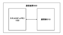
- FIG. 16 is a schematic view showing a configuration example of the communication device 500.
- a chiral magnetic material is an example of a magnetic material that can form skyrmions.
- the chiral magnetic material is a magnetic material in which the arrangement of magnetic moment when no external magnetic field is applied becomes a magnetically ordered phase (helical magnetic phase) rotating in a spiral on the traveling direction of the magnetic moment.
- the chiral magnetic material becomes a ferromagnetic phase through a crystal phase in which skirmions are arranged in a lattice.
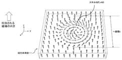
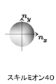
- FIG. 1 is a schematic view showing an example of skirmion 40 which is a nanoscale magnetic structure in magnetic thin film 11.
- each arrow indicates the direction of the magnetic moment in the skyrmion 40.
- the x axis and the y axis are axes orthogonal to each other, and the z axis is an axis orthogonal to the xy plane.
- the magnetic thin film 11 has a plane parallel to the xy plane.
- the magnetic moment directed in any direction in the magnetic thin film 11 constitutes the skirmion 40.
- the direction of the magnetic field applied to the magnetic thin film 11 is the positive z-direction.
- the magnetic moment of the outermost periphery of the skyrmion 40 of this example is directed to the plus z direction.
- the outermost circumference refers to the circumference of the magnetic moment directed in the same direction as the external magnetic field shown in FIG.
- the magnetic moment is arranged so as to spirally rotate from the outermost periphery toward the inner side. Furthermore, the direction of the magnetic moment gradually changes from the plus z direction to the minus z direction toward the center of the vortex as the spiral rotation is performed. Skirmion 40 is a nanoscale magnetic structure having a spiral structure of magnetic moment.
- the magnetic moments constituting the skyrmion 40 consist of the same magnetic moment in the z direction. That is, the skyrmion 40 has a magnetic structure consisting of magnetic moments in the same direction from the front surface to the back surface in the depth direction (z direction) of the closed path shape magnetic thin film 11.
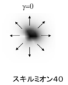
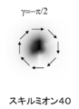
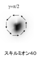
- FIGS. 2A to 2D are schematic diagrams showing skyrmions 40 with different helicity ⁇ (ie, the twisting of the magnetic moment).
- ⁇ the number of skill mions
- FIG. 2E shows how to obtain the coordinates of the magnetic moment (right hand system). Since the right-handed system is used, the n z -axis is taken from the back to the front of the drawing with respect to the n x -axis and the n y -axis. Moreover, the relationship between the density and the direction of the magnetic moment is shown in FIG. 2E.
- the skyrmion number Nsk characterizes skyrmion 40, which is a nanoscale magnetic structure having a spiral structure.
- the following [Equation 1] and [Equation 2] express the number of skill mions Nsk.
- the polar angle ⁇ (r) between the magnetic moment and the z-axis is a continuous function of the distance r from the center of the skyrmion 40.
- the polar angle ⁇ (r) varies from ⁇ to zero or from zero to ⁇ when r is varied from 0 to ⁇ .
- the vector quantity n (r) represents the direction of the magnetic moment of the skyrmion 40 at the position r.
- FIG. 2A to FIG. 2D are schematic diagrams showing skyrmions 40 with different helicity ⁇ .
- FIG. 2E shows how to obtain the coordinates of the magnetic moment (right hand system). Since the right-handed system is used, the n z -axis is taken from the back to the front of the drawing with respect to the n x -axis and the n y -axis. Moreover, the relationship between the density and the direction of the magnetic moment is shown in FIG. 2E.
- FIGS. 2A to 2D the shading indicates the direction of the magnetic moment.
- Each arrow in FIGS. 2A to 2D indicates a magnetic moment separated from the center of the skyrmion 40 by a predetermined distance.
- the magnetic structure shown in FIGS. 2A to 2D is in a state of defining a skyrmion 40.
- the lightest and darkest region indicates the magnetic moment in the direction from the back to the front of the paper.
- the magnetic moment is shown in white.
- the area with the highest density represents the magnetic moment in the direction from the front of the paper to the back.
- each magnetic moment of FIG. 2A 0
- the direction of each magnetic moment in FIG. 2C ⁇ 90 degrees for each magnetic moment in FIG. 2A (90 degrees clockwise) It is the direction of rotation.
- FIGS. 2A-2D appear different but are topologically identical magnetic structures. Skirmions 40 having the structures of FIGS. 2A to 2D are present stably once generated, and function as carriers for transmitting information in the magnetic thin film 11 to which an external magnetic field is applied.
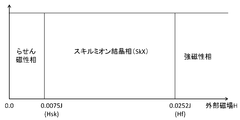
- FIG. 3 is a phase diagram showing the magnetic field dependency of the magnetic substance magnetic phase.
- the chiral magnetic material is a magnetic thin film which changes from a chiral magnetic phase to a skyrmion crystal phase (SkX) by a magnetic field strength Hsk, and changes from a skyrmion crystal phase (SkX) to a ferromagnetic phase at a high magnetic field strength Hf.
- a plurality of skyrmions 40 are aligned in a close-packed structure and occur in the xy plane.
- a is the lattice constant of the magnetic thin film 11
- D is the magnitude of the Jaroshinski-Moriya interaction, and is a physical constant inherent to the substance. Therefore, the skyrmion diameter ⁇ is a substance specific constant.
- the skyrmion diameter ⁇ is, for example, 70 nm for FeGe and 18 nm for MnSi.
- FIG. 4 shows an example of the configuration of the magnetic element 10 according to the first embodiment.
- the magnetic element 10 shown in FIG. 4 enables generation and erasure of one skyrmion 40 by pulse current.
- the presence or absence of the skyrmion 40 at a predetermined position of the magnetic thin film 11 corresponds to 1-bit information.
- the magnetic element 10 stores (stores) information using the skill muon 40.
- the magnetic element 10 of this example includes a magnetic thin film 11, an upstream electrode 12, a downstream electrode 14, a detection element 15, an erase line 95, a write line 96, a word line 97, a bit line 94, and a transistor Tr1.
- the transistor Tr1 is an example of a transistor portion for selecting the skirmion generating portion having the magnetic thin film 11, the upstream side electrode 12 and the downstream side electrode 14, the erasing portion or the detection element 15. Further, a magnetic field generating unit 20 provided outside the magnetic element 10 which is not the configuration of the magnetic element 10 is shown by a broken line.
- FIG. 4 shows (x, y, z) coordinates.
- the upstream electrode 12 is connected to one end of the magnetic thin film 11.
- the upstream electrode 12 is connected in the spreading direction of the magnetic thin film 11.
- the spreading direction of the magnetic thin film 11 refers to a direction parallel to the xy plane.
- the upstream electrode 12 may be laminated on the end of the magnetic thin film 11.
- the upstream electrode 12 may have a thin layer shape. Further, the upstream electrode 12 may have the same thickness as the magnetic thin film 11.
- the upstream electrode 12 is connected to the write line 96.
- the upstream electrode 12 is made of a conductive nonmagnetic thin film metal such as Cu, W, Ti, TiN, Al, Pt, Au or the like.
- the write line 96 is an example of the first selection line 1-A1.
- the downstream electrode 14 is separated from the upstream electrode 12 and connected to the magnetic thin film 11.
- the downstream electrode 14 in this example is connected to the other end of the magnetic thin film 11 facing the upstream electrode 12.
- the downstream electrode 14 may be connected in the spreading direction of the magnetic thin film 11.
- the downstream electrode 14 may be laminated on the end of the magnetic thin film 11.
- the upstream side electrode 12 and the downstream side electrode 14 are disposed so that a current in a direction substantially parallel to the xy plane flows to the magnetic thin film 11 when a voltage is applied.
- the downstream electrode 14 is connected to the erase line 95.
- the downstream electrode 14 is made of a conductive nonmagnetic thin film metal such as Cu, W, Ti, TiN, Al, Pt, Au or the like.
- the erase line 95 is an example of the first select line 1-A2.
- the magnetic thin film 11 develops at least a skirmion crystal phase and a ferromagnetic phase according to the applied magnetic field.
- the magnetic substance having the skirmion crystal phase and the ferromagnetic phase is a necessary condition that the skirmion 40 can be generated on the magnetic thin film 11.
- the magnetic thin film 11 is a chiral magnetic material, and is formed of FeGe or MnSi having a B20 structure, or CoZn or CoZnMn having a ⁇ Mn structure.
- the magnetic thin film 11 may have a laminated structure of magnetic and nonmagnetic materials.
- a magnetic thin film having a laminated thin film structure of a magnetic thin film and a nonmagnetic thin film is a laminated magnetic thin film in which the magnetic moment of the magnetic thin film is modulated by the spin-orbit interaction of the nonmagnetic thin film.
- the magnetic thin film 11 can be formed on a magnetic thin film formed using an MBE (Molecular Beam Epitaxy) apparatus, a sputtering apparatus, or the like using an exposure apparatus, an etching apparatus, a CMP (Chemical Mechanical Planarization) method.
- the magnetic thin film 11 has a thin film shape.
- the magnetic thin film 11 has a substantially rectangular shape with a width Wm and a length Hm on the thin film plane.
- the width Wm of the magnetic thin film 11 is 3 ⁇ > Wm ⁇ ⁇ where ⁇ is the skyrmion diameter, and the length Hm of the magnetic thin film 11 is 2 ⁇ > Wm ⁇ ⁇ .
- the magnetic thin film 11 has a recess at the end portion between the upstream electrode and the downstream electrode.
- the magnetic thin film 11 may be surrounded by a nonmagnetic insulating material or the like generally used in the semiconductor process.
- a nonmagnetic insulator thin film is provided between the magnetic thin film 11 and the magnetic thin film 11 of the adjacent magnetic element 10.
- the thickness of the magnetic thin film 11 may be, for example, about 10 times or less the diameter ⁇ of the skirmion 40.
- the transistor Tr1 is provided between the downstream electrode 14 and the erase line 95.
- the transistor Tr1 is a field effect transistor (FET).
- the gate terminal of the transistor Tr1 is connected to the word line 97.
- the transistor Tr1 prevents a leak current from flowing through the magnetic element 10 when the corresponding magnetic element 10 is not selected. As a result, it is possible to prevent erroneous writing or erroneous erasing on the magnetic element 10 not to be written. Furthermore, since the leak current can be shut off, power consumption can be reduced. Furthermore, the transistor Tr1 also serves to select the detection element 15.
- the transistor Tr1 is provided between the downstream side electrode 14 and the erase line 95 to enable data reading of the selected magnetic element 10.
- the transistor Tr1 between the upstream electrode 12 and the write line 96.
- the gate terminal of the transistor Tr1 is connected to the word line 97.
- the transistor Tr1 prevents a leak current from flowing through the magnetic element 10 when the corresponding magnetic element 10 is not selected. Also, the transistor Tr1 has a role of selecting the detection element 15, as described above.
- the transistor Tr 2 between the magnetic metal thin film 152 which is the magnetic metal of the detection element 15 and the bit line 94.
- the resistance value between the detection element 15 and the downstream electrode 14 is high.
- detecting the resistance between the magnetic metal thin film 152 of the detection element 15 and the upstream electrode 12 makes it easier to read out the change in the resistance of the detection element 15 due to the presence or absence of skirmion.
- the gate terminal of the transistor Tr2 is connected to the word line 97. A current during generation and generation of the skirmion 40 uses the transistor Tr1, and a detection of the skirmion 40 uses the transistor Tr2. In this case, two transistors are required as the magnetic element.
- the upstream electrode 12 and the downstream electrode 14 either the direction from the upstream electrode 12 to the downstream electrode 14 or the direction from the downstream electrode 14 to the upstream electrode 12 is selected to A pulse current is applied to 11.
- the magnetic element 10 applies a pulse current to the magnetic thin film 11 in the direction from the upstream electrode 12 to the downstream electrode 14 when skirmion 40 is generated in the magnetic thin film 11.
- the pulse electron flow flowing in the magnetic thin film 11 is indicated by the black line arrow.
- the electron current flows in the direction opposite to the current direction.
- the magnetic element 10 when erasing the skyrmions 40 present in the magnetic thin film 11, applies a pulse current to the magnetic thin film 11 in the direction from the downstream electrode 14 toward the upstream electrode 12.
- the magnetic thin film 11 has a recess 16 at the end 18.
- the end portion 18 in this example is an end portion of the end portion of the magnetic thin film 11 that is sandwiched by the upstream side electrode 12 and the downstream side electrode 14.
- the end 18 is an upper or lower end of the magnetic thin film 11 when the upstream electrode 12 is disposed on the right side and the downstream electrode 14 is disposed on the left.
- the recess 16 is provided at an end 18 so as to be separated from both the upstream electrode 12 and the downstream electrode 14.
- the end of the recess 16 on the downstream electrode 14 side extends to the end of the magnetic thin film 11 on the downstream electrode 14 side.
- the magnetic element 10 comprises an L-shaped magnetic thin film 11.
- a nonmagnetic thin film may be provided inside the recess 16.
- the magnetic element 10 uses one skyrmion 40 generated by current as an information storage medium.
- One skyrmion 40 can be generated from the recess 16 of the magnetic thin film 11 by the pulsed electron current.
- the corner portion facing the upstream electrode 12 is referred to as a first corner portion 24.
- a pulse current is caused to flow from the upstream electrode 12 to the downstream electrode 14. That is, a pulsed electron current is applied from the downstream electrode 14.
- skirmions 40 are generated near the first corner 24.
- the recess 16 may have a side parallel to the upstream electrode 12 or a side parallel to the downstream electrode 14.
- the first corner 24 may be an end of a side parallel to the upstream electrode 12.
- the recess 16 in this example has a rectangular shape.
- the shape of the recess 16 is not limited to a square.
- the shape of the recess 16 may be polygonal.
- each side of the recessed part 16 does not need to be a straight line.
- the first corner 24 of the recess 16 may be rounded.
- the magnetic thin film 11 becomes a ferromagnetic phase by the magnetic field generator 20. For this reason, the magnetic moment in the magnetic thin film 11 is in the same direction as the magnetic field H. However, the magnetic moment at the end of the magnetic thin film 11 is not directed in the same direction as the magnetic field H, and has a tilt relative to the magnetic field H. In particular, in the vicinity of the first corner 24 of the recess 16, the inclination of the magnetic moment changes continuously. For this reason, the first corner 24 of the magnetic thin film 11 is more susceptible to skirmion 40 than the other regions, and the skirmion 40 can be generated by a predetermined pulsed electron current.
- the first corner 24 is formed to have a predetermined internal angle.
- the internal angle of the first corner 24 is 180 ° or more.
- the internal angle of the first corner 24 in the recess 16 refers to the angle on the magnetic thin film 11 side of the first corner 24.
- the internal angle of the first corner 24 adjacent to the upstream electrode 12 is 270 °.
- the inner angle of the first corner 24 be 270 ° in the generation of the skirmion 40.
- the skirmion 40 can be erased by flowing a pulse current from the downstream electrode 14 toward the upstream electrode 12 to the magnetic thin film 11.
- the direction of the pulsed electron current is opposite to that in FIG.
- the skirmion 40 is driven to the first corner 24 and erased.
- the skirmion 40 can be chased at the first corner 24 and erased.
- the detection element 15 is a tunnel magnetoresistive element (TMR element).
- TMR element tunnel magnetoresistive element
- the detection element 15 of this example is provided between the upstream electrode 12 and the first corner 24 of the recess 16.
- the detection element 15 has a laminated structure of a nonmagnetic insulator thin film 151 formed on the magnetic thin film 11 and a magnetic metal thin film 152 made of metal formed on the nonmagnetic insulator thin film 151.
- the detection element 15 measures the value of the resistance of the nonmagnetic insulator thin film 151 between the magnetic metal thin film 152 and the magnetic thin film 11.
- the resistance value of the nonmagnetic insulator thin film 151 shows the maximum value, and when the Skirmion 40 does not exist, the resistance value of the nonmagnetic insulator thin film 151 shows the minimum value. Show.
- the high resistance (H) state and the low resistance (L) state of the detection element 15 correspond to the presence or absence of the skyrmion 40, and correspond to the information "1" and "0" stored by the memory cell.
- the detection element 15 is a tunnel magnetoresistive (TMR) element.
- TMR tunnel magnetoresistive
- the detection element 15 utilizes the effect that the resistance value of the insulator thin film sandwiched between the magnetic metal thin films depends on the state of the magnetic moment of both magnetic thin films.
- the magnetic metal thin film 152 constituting the detection element 15 has a magnetic moment in the z direction due to the magnetic field from the magnetic field generation unit 20.
- the magnetic moment of the magnetic thin film 11 is a vortex.
- the quantum effect on the tunnel electron current flowing in the nonmagnetic insulator thin film 151 is reduced. As a result, the tunnel current flowing through the nonmagnetic insulator thin film 151 is reduced.
- the resistance value of the nonmagnetic insulator thin film 151 shows the maximum value.
- a magnetic moment M in the z direction identical to the magnetic field H of the magnetic field generation unit 20 is generated in the magnetic thin film 11.
- the magnetic metal thin film 152 also generates a magnetic moment M in the z direction, which is the same as the magnetic field H of the magnetic field generation unit 20.
- a tunnel current flows more to the nonmagnetic insulator thin film 151 between the magnetic metal thin film 152 and the magnetic thin film 11 due to the quantum effect. That is, the resistance value of the nonmagnetic insulator thin film 151 exhibits the minimum value.
- the resistance value of the nonmagnetic insulator thin film 151 is higher in the presence of the skirmion 40 than in the absence of the skirmion 40. By detecting this resistance value, it is possible to detect the presence or absence of the skirmion 40 and read the information stored in the magnetic element 10.
- the magnetic metal thin film is a magnetic metal thin film such as Co, Ni, Fe or the like, or a laminated magnetic metal thin film formed of these magnetic metal thin films.
- the bit line 94 is connected to the magnetic element 10 and applies a constant current to generate a voltage according to the presence or absence of the skirmion 40 of the corresponding magnetic element 10. That is, the bit line 94 functions as a skillion detection line. Bit line 94 is an example of a second select line.
- the detection element 15 of this example was provided in contact with the top surface of the magnetic thin film 11.
- the detection element 15 may be a detection element formed so as to sandwich the nonmagnetic insulator thin film 151 between the magnetic thin film and the soft magnetic thin film.
- the direction of the magnetic moment of the soft magnetic thin film is the direction of the magnetic moment corresponding to the magnetic structure of the magnetic thin film 11. If the detection element of this structure is formed directly on the magnetic thin film 11, skirmion 40 can be detected with high sensitivity.
- the transistor Tr2 for selecting the detection element 15 is essential.
- the transistor Tr1 can not double as the selection of the detection element 15.
- FIG. 4 shows a magnetic field generation unit 20 which is a component of the skillion memory 100 according to the first embodiment.
- FIG. 4 shows (x, y, z) coordinates.
- the magnetic field generation unit 20 applies a magnetic field H to the magnetic thin film 11.
- the magnetic field generation unit 20 of this example turns the magnetic thin film 11 into a ferromagnetic phase.
- the magnetic field generation unit 20 applies a magnetic field H substantially perpendicular to the surface of the thin film magnetic thin film 11 to the magnetic thin film 11.
- the magnetic thin film 11 has a surface (one surface) parallel to the xy plane, and the magnetic field generating unit 20 generates a magnetic field H in the positive z direction as indicated by the arrow in the magnetic field generating unit 20.
- the magnetic field generating unit 20 may be provided to face the back surface of the magnetic thin film 11.
- the magnetic field generation unit 20 may be separated from or in contact with the magnetic thin film 11.
- the magnetic field generator 20 is preferably separated from the magnetic thin film 11.
- the size of the area of the magnetic field generation unit 20 facing the magnetic thin film 11 may not be the same as that of the magnetic thin film 11.
- the magnetic field generation unit 20 may also be used as a magnetic field generation unit 20 for another magnetic thin film 11.
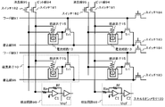
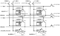
- FIG. 5A shows an example of the configuration of the skill meon memory 100 according to the first embodiment.
- the skyrmion memory 100 of this example includes the magnetic element 10 illustrated in FIG.
- the magnetic element 10 comprises an L-shaped magnetic thin film 11.
- An upstream electrode 12 and a downstream electrode 14 are provided.
- a detection element 15 is provided.
- a transistor Tr1 is provided between the downstream electrode 14 and the erase line 95.
- the present magnetic element 10 is characterized in that it comprises only one transistor.
- the transistor Tr1 is a transistor for selecting the L-shaped magnetic thin film and for selecting the detection element 15.
- the skyrmion memory 100 of this example includes a plurality of the magnetic elements 10 shown in FIG. 3 in a matrix.
- FIG. 5A shows only some of the columns and rows of the matrix.
- the skyrmion memory 100 includes a plurality of magnetic elements 10, a plurality of bit lines 94, a plurality of erase lines 95, a plurality of write lines 96, a plurality of word lines 97, a plurality of switches 181, a plurality of switches 182, and a plurality of switches 183, a plurality of switches 184 and a plurality of detection circuits 98.
- the write line 96 is connected to the magnetic element 10 and supplies a generation current for generating the skirmions 40 of the corresponding magnetic element 10. That is, the write line 96 functions as a skillion generation line.
- the erase line 95 is connected to the magnetic elements 10, and supplies an erasing current for erasing the skyrmions 40 to the corresponding magnetic elements 10. That is, the erase line 95 functions as a skirmion erase line.
- the bit line 94 is connected to the magnetic element 10 and applies a constant current to generate a voltage according to the presence or absence of the skirmion 40 of the corresponding magnetic element 10. That is, the bit line 94 functions as a skillion detection line.
- the word line 97 connects to the magnetic element 10 and selects the magnetic element 10 that generates, erases and detects skirmions 40.
- the word line 97 in this example is connected to the gate terminal of the transistor Tr1.
- a switch 181 is provided for each bit line 94.
- a switch 182 is provided for each erase line 95.
- a switch 183 is provided for each write line 96.
- a switch 184 is provided on each word line 97.
- the switches 181, 182, 183, and 184 are FETs.
- Erase line 95 and write line 96 are connected to an external pulse current source via respective switches.
- the external pulse current sources may be a common pulse current source.
- the external pulse current source may be provided for each erase line 95 or may be provided commonly to the plurality of erase lines 95.
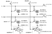
- the detection circuit 98 is connected to the bit line 94 and detects the voltage of the bit line 94.
- the detection circuit 98 may be provided for each bit line 94, or may be provided commonly for the plurality of bit lines 94.
- the detection circuit 98 of this example amplifies the voltage of the bit line 94 to detect the presence or absence of the skirmion 40.
- the detection circuit 98 includes an input resistor Rin, a feedback resistor Rf, an amplifier circuit C1 and a voltage comparison circuit C2.
- the voltage of the bit line 94 is amplified by the ratio of the input resistance Rin to the feedback resistance Rf.
- the differential voltage is amplified by inputting both the output voltage of the amplification circuit C1 and the reference voltage Vref to the voltage comparison circuit C2.
- the voltage comparison circuit C2 outputs “1” when the output voltage of the amplification circuit C1 is larger than the reference voltage Vref.
- the voltage comparison circuit C2 outputs “0” when the output voltage of the amplification circuit C1 is smaller than the reference voltage Vref.
- the upstream electrode 12 of the magnetic element 10 is connected to the corresponding write line 96.
- the downstream electrode 14 is connected to the corresponding erase line 95.
- the detection element 15 is connected to the corresponding bit line 94.
- the transistor Tr1 is provided to select the magnetic thin film 11.
- the transistor Tr1 of this example is provided between the upstream electrode 12 and the write line 96.
- the gate terminal of the transistor Tr1 is connected to the word line 97.
- the transistor Tr1 prevents a leak current from flowing through the magnetic element 10 when the corresponding magnetic element 10 is not selected.
- the leakage current generates the skill ions 40 in the non-selected magnetic elements 10 to cause erroneous writing.
- the leakage current erases the skyrmions 40 of the non-selected magnetic element 10 to cause erroneous erasure.
- the skyrmion memory 100 of this example can shut off the leak current through the magnetic element 10, and prevents erroneous writing and erroneous erasing.
- a transistor Tr1 is provided between at least one of the upstream electrode 12 and the write line 96 or between the downstream electrode 14 and the erase line 95.
- FIG. 5A shows the case where a transistor Tr1 is provided between the downstream electrode 14 and
- the transistor Tr1 between the downstream electrode 14 and the erase line 95, it is possible to select the detection element 15 of the magnetic element 10 from which data is to be read.
- the resistance value between the detection element 15 of the non-selected magnetic element 10 and the erase line 95 can be made infinite by the transistor Tr1.
- the corresponding bit line 94 of the magnetic element 10 for which data is to be read is selected, and a constant current is supplied to the bit line 94.
- the voltage of the selected bit line 94 is determined by the resistance value indicated by the detection element 15 of the magnetic element 10 in which the transistor Tr1 is turned on.
- the resistance value of all the other magnetic elements 10 connected to the selected bit line 94 is infinite because the transistor Tr1 is off.
- the voltage of the selected bit line 94 is a voltage due to the resistance value of only the TMR element of the selected magnetic element 10.
- FIG. 5B illustrates an example of the configuration of the skill meon memory 100 according to the first embodiment.
- the skyrmion memory 100 of this example is the case where the transistor Tr 2 is provided between the bit line 94 and the detection element 15.
- the transistor Tr1 is necessary to select the magnetic element 10.
- the transistor Tr1 and the transistor Tr2 are an example of a transistor unit.
- the transistor Tr1 is provided to select the magnetic thin film 11.
- the transistor Tr1 of this example is provided between the downstream electrode 14 and the erase line 95.
- the gate terminal of the transistor Tr1 is connected to the word line 97.
- the transistor Tr1 prevents a leak current from flowing through the magnetic element 10 when the corresponding magnetic element 10 is not selected.
- the skyrmion memory 100 of this example can shut off the leak current through the magnetic element 10.
- the skyrmion memory 100 of this example can prevent erroneous writing and erasing of the skyrmion 40 and, at the same time, can suppress an increase in power consumption.
- the transistor Tr2 is provided to directly select the detection element 15.
- the transistor Tr1 of this circuit can not select the detection element 15.
- the transistor Tr 2 is provided between the detection element 15 and the bit line 94.
- the gate terminal of the transistor Tr2 is connected to the word line 97.
- the transistor Tr1 for selecting the magnetic thin film 11 is provided between at least one of the upstream electrode 12 and the write line 96 or between the downstream electrode 14 and the erase line 95. .
- the leak current of the skill-ion memory 100 can be shut off, and erroneous writing and erroneous erasing can be prevented.
- the detection element 15 can be further selected.
- the magnetic element 10 is a single transistor Tr 1, which can shut off the leak current and prevent the erroneous writing, and can generate, erase and detect the skirmion 40.
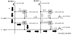
- the switch 183 of the upper write line 96 is turned on.
- the switch 182 of the left erase line 95 is turned on.
- the switch 184 of the upper word line 97 is turned on.
- a pulse current for skirmion generation is applied to the upper write line 96.
- the pulse current is applied only to the upper left magnetic element 10.
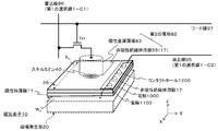
- FIG. 6 shows the configuration of the skill meon memory 600 according to the first comparative example.
- the skyrmion memory 600 of this example does not have the transistor Tr1.
- the skirmion memory 600 of the present example causes the generated current Ig to flow to the upper left magnetic element 10 by turning on the switch 182 and the switch 184.
- the generated current Ig is indicated by a solid arrow.
- the leakage current IL is indicated by an open arrow. Since the magnetic thin film 11 is a metal material, the leak current IL has a large value.
- the leak current IL causes erroneous writing, erroneous erasure, and increased power consumption of the skirmion 40.
- the current direction of the leakage current IL of the magnetic element 10 at the upper right and lower left is the current in the generation direction of the skyrmion 40, so the skyrmion 40 is generated in the magnetic element 10 at the upper right Resulting in. That is, erroneous writing occurs.
- the skyrmion 40 is present when the skyrmion 40 exists in the lower right magnetic element 10. Erase the That is, erroneous erasure occurs. Also, the skyrmion memory 600 has a large number of magnetic elements 10 in a matrix. Since the leak current IL is generated through each of the magnetic elements 10, the entire skillion memory 600 consumes a large amount of power.
- the transistor Tr1 according to the first embodiment is provided in at least one of between the upstream electrode 12 and the write line 96 or between the downstream electrode 14 and the erase line 95. That is, while the transistor Tr1 of this example is provided for each of the magnetic thin films 11 that generate one skirmion 40, the switches 182 and 184 are provided for two or more of the magnetic thin films 11. There is a big difference in Thereby, the skyrmion memory 100 of the first embodiment can shut off the leak current through the magnetic element 10. As described above, by blocking the leakage current through the magnetic element 10, the skyrmion memory 100 according to the present specification can prevent erroneous writing and prevent erroneous erasure, and has excellent performance with low power consumption. Indicates Furthermore, the transistor Tr1 functions as a transistor that selects the detection element 15. As a result, memory cells can be made smaller and higher density can be achieved.
- FIG. 7 is a schematic view showing the magnetic element 10 according to the second embodiment.
- the magnetic element 10 of this example enables the generation of the skirmion 40.
- the magnetic element 10 stores bit information using the skyrmion 40.
- the presence or absence of the skyrmion 40 in the magnetic thin film 11 corresponds to 1-bit information.
- the magnetic element 10 of this example includes the magnetic thin film 11, the current path 13, the detection element 15, the nonmagnetic insulator thin film 17, the electrode 1000, the electrode 1100, the contact hole 1200, the write line 96, the erase line 95, and the word line 97. And a transistor Tr1.
- the magnetic field generation unit 20 indicated by a broken line is not the configuration of the magnetic element 10.
- the magnetic thin film 11 may be surrounded by an insulating silicon oxide material or the like generally used in a semiconductor process. In addition, the magnetic thin film 11 surrounds all directions with a nonmagnetic material.
- the current path 13 surrounds a region including the end of the magnetic thin film 11 on one surface of the magnetic thin film 11.
- the current path 13 may be electrically isolated from the magnetic thin film 11 by using a nonmagnetic insulator thin film 17 or the like of a nonmagnetic material.
- the current path 13 in this example is a current circuit formed in a U-shape.
- the U-shape may be a shape including not only a shape having rounded corners but also a right angle as in this example.
- the current path 13 may not form a closed region in the xy plane.
- the combination of the current path 13 and the end 18 may form a closed region on the surface of the magnetic thin film 11. In the current path 13, current flows in the direction indicated by the arrow C.
- the current path 13 is formed of a nonmagnetic metal material such as Cu, W, Ti, Al, Pt, Au, TiN, AlSi.
- a U-shaped region where the region surrounded by the current path 13 includes the end of the magnetic thin film 11 is particularly referred to as an end region A.
- the current path 13 in this example crosses the end of the magnetic thin film 11 at least once from the nonmagnetic thin film side to the magnetic thin film 11 in the xy plane, and from the magnetic thin film 11 to the nonmagnetic thin film It has a continuous conducting path which traverses at least once on the side.
- the current path 13 surrounds a region including the end of the magnetic thin film 11.
- the magnetic field strength in the end region A is set to Ha.
- the current C flowing through the current path 13 generates a magnetic field (-Hc) from the front surface to the back surface of the magnetic thin film 11 in the U-shaped region surrounded by the current path 13.
- the direction of this magnetic field is negative with respect to the z direction. Since the direction of the magnetic field induced by the current flowing through the current path 13 is opposite to the direction (plus direction of the z axis) of the uniform magnetic field H from the magnetic field generation unit 20, the magnetic thin film A weak magnetic field Ha is generated from the back surface of the surface 11 to the surface direction.
- Equation 3) Ha H-Hc
- the skirmion 40 can be generated in the end area A.
- the current path 13 may have a laminated structure of a nonmagnetic insulator thin film formed on the magnetic thin film 11 and a nonmagnetic metal thin film formed on the nonmagnetic insulator thin film.
- the nonmagnetic insulator thin film included in the current path 13 may be the same nonmagnetic insulator thin film as the nonmagnetic insulator thin film 151 included in the detection element 15.
- the nonmagnetic insulator thin film included in the current path 13 and the nonmagnetic insulator thin film 151 have the same process, material, and / or thickness.
- One end of the current path 13 is the current path upstream end portion 131 connected to the write line 96.
- the write line 96 is an example of the first select line 1-B1.
- the other end is the current path downstream end 132 connected to the erase line 95.
- the erase line 95 is an example of the first select line 1-B2.
- the current path upstream end portion 131 may be electrically connected to the magnetic thin film 11.
- the current path upstream end portion 131 is electrically connected to the electrode 1100 and electrically connected to the electrode 1000 via the contact hole 1200.
- the electrodes 1000 and 1100 are made of a conductive nonmagnetic metal thin film such as Cu, W, Ti, TiN, Al, Pt, Au or the like.
- the transistor Tr 1 is provided between the current path upstream end 131 and the write line 96 or between the current path downstream end 132 and the erase line 95.
- the gate terminal of the transistor Tr1 is connected to the word line 97.
- the transistor Tr1 prevents a leak current from flowing through the magnetic element 10 when the corresponding magnetic element 10 is not selected. Thereby, the skyrmion memory 100 of this example can shut off the leak current through the magnetic element 10. That is, the transistor Tr1 is provided in at least one of between the current path upstream end 131 and the write line 96 or between the current path downstream end 132 and the erase line 95.
- the detection element 15 is a tunnel magnetoresistive element (TMR element).
- TMR element tunnel magnetoresistive element
- the detection element 15 is a detection element having the same laminated structure as that of the first embodiment.
- the detection element 15 of this example is provided between the U-shaped current path 13 and the end 18 of the magnetic thin film 11.
- the detection function of the skill muon 40 is the same as the detection function in the first embodiment.
- the magnetic thin film 11 is used as the other electrode.
- an electrode 1000 of nonmagnetic metal is provided at the end of the magnetic thin film 11.
- the electrode 1000 may be provided on the spread portion of the magnetic thin film. It may be laminated on the end of the magnetic thin film 11.
- a contact hole 1200 may be provided for electrical connection to the electrode 1000, and an electrode 1100 may be provided on the upper layer.
- the bit line 94 is connected to the magnetic element 10 and applies a constant current to generate a voltage according to the presence or absence of the skirmion 40 of the corresponding magnetic element 10. That is, the bit line 94 functions as a skillion detection line. Bit line 94 is an example of a second select line.
- the transistor Tr1 can be selected between the current path upstream end portion 131 and the write line 96 to select the detection element 15 of the magnetic element 10 from which data is to be read.
- the resistance value between the detection element 15 of the non-selected magnetic element 10 and the write line 96 can be made infinite by the transistor Tr1. As a result, only the resistance value of the detection element 15 of the selected magnetic element 10 can be read.
- FIG. 8 shows an example of the configuration of the skill-ion memory 100 according to the second embodiment.
- the skyrmion memory 100 of this example is different from the skyrmion memory 100 according to the first embodiment in that a magnetic element 10 that generates and erases skyrmions 40 using a U-shaped current path 13 is used. That is, the magnetic element 10 of this example generates and cancels skyrmions 40 by the current-induced local magnetic field.
- the skyrmion memory 100 of the present example is provided with a U-shaped current path 13 including the end of the magnetic thin film. In the case of a current path having a shape that does not include the magnetic thin film end, skirmion 40 can not be generated.
- the skyrmion memory 100 of this example includes a plurality of magnetic elements 10 shown in FIG. 7 in a matrix. FIG. 8 shows only some of the plurality of columns and rows of the matrix.
- the skyrmion memory 100 includes a plurality of magnetic elements 10, a plurality of bit lines 94, a plurality of erase lines 95, a plurality of write lines 96, a plurality of word lines 97, a plurality of switches 181, a plurality of switches 182, and a plurality of switches 183, a plurality of switches 184 and a plurality of detection circuits 98.
- the write line 96 is connected to the magnetic element 10 and supplies a generation current for generating the skirmions 40 of the corresponding magnetic element 10. That is, the write line 96 functions as a skillion generation line.
- the erase line 95 is connected to the magnetic elements 10, and supplies an erasing current for erasing the skyrmions 40 to the corresponding magnetic elements 10. That is, the erase line 95 functions as a skirmion erase line.
- the word line 97 connects to the magnetic element 10 and selects the magnetic element 10 that generates, erases and detects skirmions 40.
- the word line 97 in this example is connected to the gate terminal of the transistor Tr1.
- a switch 181 is provided for each bit line 94.
- a switch 182 is provided for each erase line 95.
- a switch 183 is provided for each write line 96.
- a switch 184 is provided on each word line 97.
- the switches 181, 182, 183, and 184 are FETs.
- Erase line 95 and write line 96 are connected to an external pulse current source via respective switches.
- the external pulse current sources may be a common pulse current source.
- the external pulse current source may be provided for each erase line 95 or may be provided commonly to the plurality of erase lines 95.
- the detection circuit 98 is connected to the bit line 94 and detects the voltage of the bit line 94.
- the detection circuit 98 may be provided for each bit line 94, or may be provided commonly for the plurality of bit lines 94.
- the detection circuit 98 of this example amplifies the voltage of the bit line 94 to detect the presence or absence of the skirmion 40.
- the detection circuit 98 includes an input resistor Rin, a feedback resistor Rf, an amplifier circuit C1 and a voltage comparison circuit C2.
- the voltage of the bit line 94 is amplified by the ratio of the input resistance Rin to the feedback resistance Rf.
- the differential voltage is amplified by inputting both the output voltage of the amplification circuit C1 and the reference voltage Vref to the voltage comparison circuit C2.
- the voltage comparison circuit C2 outputs “1” when the output voltage of the amplification circuit C1 is larger than the reference voltage Vref.
- the voltage comparison circuit C2 outputs “0” when the output voltage of the amplification circuit C1 is smaller than the reference voltage Vref.
- FIG. 9 shows an example of the configuration of the skill-ion memory 600 according to the second comparative example.
- the skyrmion memory 600 of this example does not have the transistor Tr1.
- the skirmion memory 600 of the present example causes the generated current Ig to flow through the magnetic element 10 by turning on the switch 182 and the switch 183.
- the generated current Ig is indicated by a solid arrow.
- the leakage current IL is indicated by an open arrow. Since the magnetic thin film 11 is a metal material, the leak current IL has a large value.
- the leak current IL is a cause of causing erroneous write, erroneous erase, and increase in power consumption of the skirmion 40 as in the first comparative example.
- the transistor Tr1 according to the second embodiment is provided between the current path upstream end 131 and the write line 96 or between the current path downstream end 132 and the erase line 95. That is, while the transistor Tr1 of this example is provided for each of the magnetic thin films 11 that generate one skirmion 40, the switches 182 and 184 are provided for two or more of the magnetic thin films 11. There is a big difference in Thereby, the skyrmion memory 100 of the second embodiment can shut off the leak current through the magnetic element 10. As described above, the skillion memory 100 according to the present specification can prevent erroneous writing and erroneous erasure of the skillion 40 by blocking the leakage current through the magnetic element 10, and has excellent performance with low power consumption. Have. Furthermore, the transistor Tr1 functions as a transistor that selects the detection element 15. As a result, memory cells can be made smaller and higher density can be achieved.
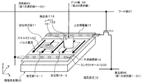
- FIG. 10 is a schematic view showing an example of the magnetic element 10 according to the third embodiment.
- the magnetic element 10 of this example enables generation of the skyrmions 40 using local heat.
- the magnetic element 10 of this example uses the skyrmion 40 to store bit information.
- the presence or absence of the skyrmion 40 in the magnetic thin film 11 corresponds to 1-bit information.
- the magnetic element 10 of this example includes the magnetic thin film 11, the second electrode 82, the nonmagnetic insulator thin film 17, the electrode 1000, the electrode 1100, the contact hole 1200, the write line 96, the erase line 95, the word line 97, and the transistor. It has Tr1.
- the write line 96 doubles as a bit line which is an example of a second select line.
- the second electrode 82 includes a nonmagnetic insulator thin film 55 provided in contact with the upper portion of the other surface 26 of the magnetic thin film 11 and a magnetic metal thin film 83 provided in contact with the upper portion of the nonmagnetic insulator thin film 55. And a laminated structure thin film.
- the detection element doubles as the second electrode 82.
- the magnetic field generation unit 20 indicated by a broken line is not the configuration of the magnetic element 10.
- the magnetic metal thin film 83 is a cylindrical magnetic metal thin film.
- the circular cross-sectional area of the magnetic metal thin film 83 is the area in contact with the other surface 26 of the magnetic thin film 11, and the radius of the circular cross section of the magnetic metal thin film 83 corresponds to the spot size radius of the local thermal energy.
- a nonmagnetic insulator thin film 55 is formed between the magnetic metal thin film 83 and the magnetic thin film 11.
- the magnetic thin film 11 is a flat plate parallel to the xy plane.
- the magnetic metal thin film 83 is a magnetic metal thin film made of Co, Ni, Fe, or a laminated magnetic metal thin film made of these magnetic metal thin films.
- the magnetic thin film 11 may be connected to a reference terminal set to a reference potential.
- the electrode 1000 is connected to the other end of the magnetic thin film 11.
- the electrode 1000 may be connected in the spreading direction of the magnetic thin film 11. It is connected to the electrode 1100 via the contact hole 1200.
- the electrode 1100 is connected to the reference potential.
- the electrodes 1000 and 1100 are made of a conductive nonmagnetic metal thin film such as Cu, W, Ti, TiN, Al, Pt, Au or the like.
- the Joule heat generated in the nonmagnetic insulator thin film 55 heats the magnetic material thin film 11 when a pulse current flows through the nonmagnetic insulator thin film 55 of the second electrode 82.
- Local heat can be generated in the nonmagnetic insulator thin film 55 by the circular cross-sectional size of the magnetic metal thin film 83.
- the pulsatile heat enables the generation and elimination of skyrmions 40 by controlling the heat energy.
- the second electrode 82 doubles as a detection element.
- the second electrode 82 is a tunnel magnetoresistive element (TMR element).
- the detection element 15 is a detection element having the same laminated structure as that of the first embodiment.
- the detection function of the skill muon 40 is the same as the detection function in the first embodiment.
- the magnetic thin film 11 is used as the other electrode.
- the nonmagnetic metal thin film electrode 1000 is provided at the end of the magnetic thin film 11.
- the electrode 1000 may be provided on the spread portion of the magnetic thin film 11.
- a contact hole 1200 may be provided for electrical connection to the electrode 1000, and an electrode 1100 may be provided on the upper layer.
- the electrode 1000 or the electrode 1100 is connected to the erase line 95.
- the transistor Tr1 is provided between the magnetic metal thin film 83 of the second electrode 82 and the write line 96. It is a major feature of the magnetic element 10 that the write line 96 doubles as a bit line which is an example of a second select line.
- the gate terminal of the transistor Tr1 is connected to the word line 97.
- the transistor Tr1 prevents a leak current from flowing through the magnetic element 10 when the corresponding magnetic element 10 is not selected. Thereby, the skyrmion memory 100 of this example can shut off the leak current through the magnetic element 10. That is, the transistor Tr1 is provided at least one of between the second electrode 82 and the write line 96 or between the magnetic thin film 11 and the erase line 95.
- the write line 96 in this example is an example of the first select line 1-C1.
- the erase line 95 in this example is an example of the first select line 1-C2.
- the transistor Tr1 between the second electrode 82 and the write line 96, the detection element 15 of the magnetic element 10 from which data is to be read can be selected.
- the resistance value of the write line 96 and the erase line 95 of the magnetic element 10 which is connected to the write line 96 but not selected by the transistor Tr1 can be infinite. As a result, only the resistance value of the detection element 15 of the selected magnetic element 10 can be read.
- the second electrode 82 of the generation unit that generates the skirmion 40 can double as the detection element 15.
- write line 96 can double as a bit line, and wiring space can be significantly reduced.
- the area of the magnetic thin film 11 can be reduced.
- the third embodiment can realize a high density memory element.
- FIG. 11 shows an example of the configuration of the skill meon memory 100 according to the third embodiment.
- the skyrmion memory 100 according to the present embodiment is different from the skyrmion memory 100 according to the first and second embodiments in that the magnetic element 10 generates and erases the skyrmion 40 by applying local heat to the magnetic thin film 11. It is different.
- the magnetic element 10 shown in FIG. 10 may be used as the magnetic element 10 of this example.
- the magnetic element 10 of this example is different from the other examples in principle of generating and erasing Squirmion 40, the method of blocking the basic leak current and the method of selecting the detecting element 15 are the first to the second examples. The same as in the case of the second example.
- the magnetic thin film 11 is connected to the reference potential 1300 via the erase line 95.
- the transistor Tr1 is provided between the magnetic element 10 and the write line 96. Also, the transistor Tr1 may be provided between the magnetic element 10 and the erase line 95. Even in this case, the transistor Tr1 can shut off the leakage current of the magnetic element 10. It is also possible to detect the skyrmion 40 of the selected magnetic element.
- the transistor Tr1 is provided between at least one of the second electrode 82 and the write line 96 or between the magnetic thin film 11 and the erase line 95.
- FIG. 12 shows the configuration of the skill-ion memory 600 according to comparative example 3.
- the skyrmion memory 600 of this example does not have the transistor Tr1.
- the skirmion memory 600 of this example causes the generated current Ig to flow through the magnetic element 10 by turning on the switch 182 and the switch 184.
- the generated current Ig is indicated by a solid arrow.
- the leak current IL causes erroneous write, erroneous erase, and increase in power consumption of the skirmion 40 as in the first comparative example.
- erroneous writing and erroneous erasing of the skyrmion 40 occur depending on the magnitude of the leakage current IL.
- the transistor Tr1 according to the third embodiment is provided between the second electrode 82 and the write line 96.
- the skyrmion memory 100 of the first embodiment can shut off the leak current through the magnetic element 10.
- the skillion memory 100 according to the present specification prevents erroneous writing and erroneous erasing, and has excellent performance with low power consumption.
- FIG. 13 is a schematic view showing an example of the magnetic element 10 according to the fourth embodiment.
- the magnetic element 10 of this example enables the transfer of the skirmion 40.
- a configuration example of the magnetic element 10 in which the direction of the current flowing between the upstream side electrode 12 and the downstream side electrode 14 is arranged substantially perpendicular to the direction of transferring the skyrmion 40 is shown as a lateral current arrangement.
- the magnetic element 10 of this example includes the magnetic thin film 11, the upstream electrode 12, the downstream electrode 14, the detection element 15, the stabilizer 19-1, the stabilizer 19-2, the contact hole 1200, the write line 96, the erase line And 95, a bit line 94, a word line 97, and a transistor Tr1.
- the skyrmions 40 in the magnetic thin film 11 can be reduced to stable portions 19-1 (first stable portions) or stable portions 19-2 of the magnetic thin film 11 (first Can be transferred and placed in the second stabilizer).
- a major feature is that the direction of the current flowing between the upstream side electrode 12 and the downstream side electrode 14 is a lateral current arrangement in which the direction of the current is substantially perpendicular to the direction of transferring the skyrmion 40.
- the detection element 15 of this example is provided corresponding to one of the plurality of stabilizing portions 19.
- the presence or absence of skyrmions 40 in the stable portion 19-2 of the magnetic thin film 11 in which the detection element 15 is present corresponds to 1-bit information.
- the magnetic field generation unit 20 indicated by a broken line is not the configuration of the magnetic element 10.
- the magnetic thin film 11 has two stable portions 19.
- the two stable portions 19 are provided in the region of the magnetic thin film 11 sandwiched by the upstream electrode 12 and the downstream electrode 14.
- the magnetic thin film 11 of the present example has a stable portion 19-1 and a stable portion 19-2.
- the stable portion 19 refers to a region where the skyrmions 40 can exist more stably than the other regions of the magnetic thin film 11.
- the stabilizing unit 19 may point to an area where the skirmion 40 stays at that location unless the skirmion 40 is externally powered by, for example, a current or the like.
- the magnetic field strength generated from the magnetic field generation unit 20 can be realized by setting the magnetic field strength weaker than the magnetic field strength around the stable portion 19 as described below.
- the stabilizing unit 19 may indicate an area isolated by any barrier.
- This barrier can be realized by providing the upstream side electrode 12 and the downstream side electrode 14 with a protruding portion that protrudes inside the magnetic thin film 11.
- Each stable portion 19 occupies a predetermined range on the surface of the magnetic thin film 11 parallel to the xy plane.
- the magnetic element 10 can transfer the skirmion 40 between the plurality of stabilizing portions 19 by the transfer current.
- the magnetic field applied to the stable portion 19-1 and the stable portion 19-2 of the magnetic thin film 11 is a magnetic field Ha smaller than the magnetic field strength H applied to the other region of the magnetic thin film 11.
- the magnetic field generation unit 20 is used such that the magnitude of the magnetic moment of the region facing the stable portion 19 is smaller than that of the other regions.
- the upstream electrode 12 is made of nonmagnetic metal connected to the magnetic thin film 11.
- the upstream electrode 12 is connected in the spreading direction of the magnetic thin film 11.
- the spreading direction of the magnetic thin film 11 refers to a direction parallel to the xy plane.
- the upstream electrode 12 may have a thin layer shape. Further, the upstream electrode 12 may have the same thickness as the magnetic thin film 11.
- the downstream electrode 14 is made of nonmagnetic metal separated from the upstream electrode 12 and connected to the magnetic thin film 11.
- the downstream electrode 14 is connected in the spreading direction of the magnetic thin film 11.
- the upstream side electrode 12 and the downstream side electrode 14 are disposed so that a transfer current in a direction substantially parallel to the xy plane flows to the magnetic thin film 11 when a voltage is applied.
- the upstream electrode 12 and the downstream electrode 14 are used to transfer skirmions 40 in the magnetic thin film 11. Note that at least one of the upstream side electrode 12 and the downstream side electrode 14 in the present example also functions as an electrode that causes a current to flow to the detection element 15 that detects the position of the skirmion 40.
- the detection element 15 of this example is a tunnel magnetoresistive element (TMR element).
- TMR element tunnel magnetoresistive element
- the detection element 15 is located in at least one stabilizer.
- the detection element 15 of this example has a laminated structure of a nonmagnetic insulator thin film 151 in contact with the surface of the magnetic thin film 11 at the position of the stable portion 19-2 and a magnetic metal thin film 152. In this example, the detection element 15 is provided only in the stable portion 19-2 of the two stable portions 19.
- the transistor Tr 1 is provided between the upstream electrode 12 and the write line 96 or between the downstream electrode 14 and the erase line 95.
- the gate terminal of the transistor Tr1 is connected to the word line 97.
- the transistor Tr1 prevents a leak current from flowing through the magnetic element 10 when the corresponding magnetic element 10 is not selected.
- the write line 96 is an example of the first select line 1-D1.
- the erase line 91 is an example of the first select line 1-D2.
- the transistor Tr1 between the upstream electrode 12 and the write line 96 or between the downstream electrode 14 and the erase line 95, it is possible to select the detection element 15 of the magnetic element 10 to read data.
- the resistance value between the detection element 15 of the magnetic element 10 which is connected to the bit line 94 but not selected by the transistor Tr1 and the write line 96 can be infinite. As a result, only the resistance value of the detection element 15 of the selected magnetic element 10 can be read.
- the write line 96 is connected to the upstream electrode 12.
- the write line 96 may be connected to the upstream electrode 12 via the transistor Tr1.
- Write line 96 carries a lateral current for moving skirmion 40.
- the current from the write line 96 moves the skirmion 40 from the stabilizer 19-1 to the stabilizer 19-2.
- the detection element 15 present in the stabilizing unit 19-2 determines that the skyrmion 40 is present. That is, the stored data is in the "1" state.
- the erase line 95 is connected to the downstream electrode 14.
- the erase line 95 may be connected to the downstream side electrode 14 via the transistor Tr1.
- the erase line 95 carries a lateral current for moving the skill ions 40.
- the current from the erase line 95 moves the skirmion 40 from the stabilizer 19-2 to the stabilizer 19-1.
- the detection element 15 located in the stabilizing unit 19-2 determines that the skill muon 40 does not exist. That is, the stored data is in the zero state.
- the bit line 94 can also be connected to the detection element 15 to generate the skirmion 40.
- the bit line 94 of this example generates skirmion 40 by applying heat to the portion of the stable portion 19-2 of the magnetic thin film 11. Further, the bit line 94 functions as a bit line 94 for detecting whether or not the skirmion 40 exists in the stabilizing unit 19-2 corresponding to the detecting element 15.
- Bit line 94 is an example of a second select line.
- FIG. 14 illustrates an example of the configuration of the skill meon memory 100 according to the fourth embodiment.
- the skyrmion memory 100 of this example is different from the skyrmion memory 100 according to the first to third embodiments in that the magnetic element 10 having two stable portions of the skirmion 40 is used.
- the magnetic element 10 of the present example has two stable portions of the skirmion 40, the method of basically blocking the leakage current and the method of selecting the detection element are the same as those of the first and second embodiments. It is.
- the transistor Tr1 of this example is provided between the upstream electrode 12 and the write line 96.
- the transistor Tr1 in this case can also be used as a selection of detection elements.
- the transistor Tr1 may be provided between the downstream side electrode 14 and the erase line 95.
- FIG. 15 shows a skill meon memory 600 according to comparative example 4.
- the skyrmion memory 600 of this example does not have the transistor Tr1.
- the skirmion memory 600 of the present example causes the generated current Ig to flow through the magnetic element 10 by turning on the switch 182 and the switch 183.
- the generated current Ig is indicated by a solid arrow.
- the leakage current IL is indicated by an open arrow. Since the magnetic thin film 11 is a metal material, the leak current IL has a large value.
- the leak current IL is a cause of causing erroneous write, erroneous erase, and increase in power consumption of the skirmion 40 as in the first comparative example.
- the transistor Tr1 according to the fourth embodiment is provided between the upstream electrode 12 and the write line 96 or between the downstream electrode 14 and the erase line 95.
- the skyrmion memory 100 of the fourth embodiment can shut off the leak current through the magnetic element 10.
- the skillion memory 100 according to the present specification prevents erroneous writing and erroneous erasing, and has excellent performance with low power consumption.
- the transistor Tr1 functions as a transistor that selects the detection element 10. As a result, memory cells can be made smaller and higher density can be achieved.
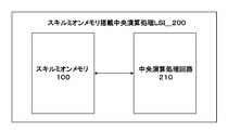
- FIG. 16 is a schematic view showing a configuration example of the central processing LSI LSI 200 equipped with the skyrmion memory.
- the central processing LSI LSI 200 equipped with a skill memory memory comprises a skill memory 100 and a central processing circuit 210.
- the central processing circuit 210 is, for example, a CMOS-LSI device.
- the central processing circuit 210 has at least one of the functions of writing data to the skillion memory 100 and reading data from the skillion memory 100.
- the skyrmion memory 100 may be stacked above the field effect transistor of the central processing LSI LSI 200 with the skyrmion memory.
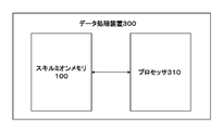
- FIG. 17 is a schematic view showing a configuration example of the data processing device 300.
- the data processing device 300 includes a skillion memory 100 and a processor 310.
- the processor 310 includes, for example, digital circuits that process digital signals.
- the processor 310 has at least one of the functions of writing data to the skillion memory 100 and reading data from the skillion memory 100.
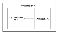
- FIG. 18 is a schematic view showing a configuration example of the data recording device 400.
- the data recording device 400 includes a skill-ion memory 100 and an input / output device 410.
- the data recording device 400 is, for example, a hard disk or a memory device such as a USB memory.
- the input / output device 410 has at least one of the function of writing data from the outside into the skillion memory 100 and the function of reading data from the skillion memory 100 and outputting the data to the outside.
- FIG. 19 is a schematic view showing a configuration example of the communication device 500.
- the communication device 500 refers to all devices having a communication function with the outside, such as a mobile phone, a smartphone, and a tablet type terminal, for example.
- Communication device 500 may be portable or non-portable.
- Communication device 500 includes skill mion memory 100 and communication unit 510.
- Communication unit 510 has a communication function with the outside of communication device 500.
- the communication unit 510 may have a wireless communication function, may have a wired communication function, and may have both wireless communication and wired communication functions.
- Communication unit 510 operates based on a function of writing data received from the outside into skillmion memory 100, a function of transmitting data read out from skillmion memory 100 to the outside, and control information stored by skillmion memory 100. Have at least one of the features.
- a magnetic element capable of generating, erasing and detecting the skyrmion 40 with high speed and low power consumption, a nonvolatile skyrmion memory 100 to which the magnetic element is applied, a central processing LSI LSI with onboard skyrmion memory 200, a data processor 300, a data storage device 400 and a communication device 500 can be provided.
Landscapes
- Engineering & Computer Science (AREA)
- Computer Hardware Design (AREA)
- Manufacturing & Machinery (AREA)
- Semiconductor Memories (AREA)
- Hall/Mr Elements (AREA)
- Mram Or Spin Memory Techniques (AREA)
Priority Applications (2)
| Application Number | Priority Date | Filing Date | Title |
|---|---|---|---|
| KR1020197014368A KR102255871B1 (ko) | 2016-11-18 | 2017-11-02 | 자기 소자, 스커미온 메모리, 스커미온 메모리가 장착된 중앙 처리 lsi, 데이터 기록 장치, 데이터 처리 장치, 및 데이터 통신 장치 |
| US16/416,317 US10658426B2 (en) | 2016-11-18 | 2019-05-20 | Magnetic element, skyrmion memory, skyrmion memory-mounted central processing LSI, data recording apparatus, data processing apparatus, and data communication apparatus |
Applications Claiming Priority (2)
| Application Number | Priority Date | Filing Date | Title |
|---|---|---|---|
| JP2016-225281 | 2016-11-18 | ||
| JP2016225281A JP6712804B2 (ja) | 2016-11-18 | 2016-11-18 | 磁気素子、スキルミオンメモリ、スキルミオンメモリ搭載中央演算処理lsi、データ記録装置、データ処理装置およびデータ通信装置 |
Related Child Applications (1)
| Application Number | Title | Priority Date | Filing Date |
|---|---|---|---|
| US16/416,317 Continuation US10658426B2 (en) | 2016-11-18 | 2019-05-20 | Magnetic element, skyrmion memory, skyrmion memory-mounted central processing LSI, data recording apparatus, data processing apparatus, and data communication apparatus |
Publications (1)
| Publication Number | Publication Date |
|---|---|
| WO2018092610A1 true WO2018092610A1 (ja) | 2018-05-24 |
Family
ID=62146595
Family Applications (1)
| Application Number | Title | Priority Date | Filing Date |
|---|---|---|---|
| PCT/JP2017/039829 Ceased WO2018092610A1 (ja) | 2016-11-18 | 2017-11-02 | 磁気素子、スキルミオンメモリ、スキルミオンメモリ搭載中央演算処理lsi、データ記録装置、データ処理装置およびデータ通信装置 |
Country Status (4)
| Country | Link |
|---|---|
| US (1) | US10658426B2 (enExample) |
| JP (1) | JP6712804B2 (enExample) |
| KR (1) | KR102255871B1 (enExample) |
| WO (1) | WO2018092610A1 (enExample) |
Cited By (1)
| Publication number | Priority date | Publication date | Assignee | Title |
|---|---|---|---|---|
| JP2024519446A (ja) * | 2021-05-05 | 2024-05-14 | インターナショナル・ビジネス・マシーンズ・コーポレーション | 調整用のトポロジカル・スピン・テクスチャを有する磁性層を備えた抵抗メモリ・デバイス |
Families Citing this family (6)
| Publication number | Priority date | Publication date | Assignee | Title |
|---|---|---|---|---|
| JP7149191B2 (ja) * | 2019-01-16 | 2022-10-06 | 株式会社アルバック | CoZnMn膜の形成方法、および、CoZnMnターゲット |
| JP2021033579A (ja) * | 2019-08-22 | 2021-03-01 | 国立大学法人大阪大学 | 演算装置 |
| JP7586694B2 (ja) * | 2020-12-01 | 2024-11-19 | Tdk株式会社 | 磁気アレイ |
| KR102517665B1 (ko) * | 2021-07-05 | 2023-04-05 | 한국표준과학연구원 | 스커미온 생성, 소거 및 이동 장치 |
| CN116820390A (zh) * | 2022-03-21 | 2023-09-29 | 中电海康集团有限公司 | 一种存算器件、计数器、移位累加器和存内乘加结构 |
| CN115527576A (zh) * | 2022-08-30 | 2022-12-27 | 香港中文大学(深圳) | 一种基于磁隧道结产生及擦除单个斯格明子的方法 |
Citations (7)
| Publication number | Priority date | Publication date | Assignee | Title |
|---|---|---|---|---|
| JP2004153182A (ja) * | 2002-10-31 | 2004-05-27 | Toshiba Corp | 磁気メモリ |
| JP2013243336A (ja) * | 2012-01-30 | 2013-12-05 | Quantu Mag Consultancy Co Ltd | Mtj素子及びその製法、並びにmramデバイス |
| WO2016021349A1 (ja) * | 2014-08-07 | 2016-02-11 | 国立研究開発法人理化学研究所 | 磁気記憶媒体およびデータ記録装置 |
| WO2016035579A1 (ja) * | 2014-09-02 | 2016-03-10 | 国立研究開発法人理化学研究所 | 磁気素子、スキルミオンメモリ、スキルミオンメモリデバイス、固体電子デバイス、データ記録装置、データ処理装置およびデータ通信装置 |
| WO2016035758A1 (ja) * | 2014-09-04 | 2016-03-10 | 国立研究開発法人理化学研究所 | 磁気素子、スキルミオンメモリ、スキルミオンメモリデバイス、スキルミオンメモリ搭載固体電子デバイス、データ記録装置、データ処理装置および通信装置 |
| WO2016067744A1 (ja) * | 2014-10-28 | 2016-05-06 | 国立研究開発法人理化学研究所 | 磁気素子、スキルミオンメモリ、スキルミオンメモリデバイス、スキルミオンメモリ搭載固体電子デバイス、データ記録装置、データ処理装置および通信装置 |
| JP5985728B1 (ja) * | 2015-09-15 | 2016-09-06 | 株式会社東芝 | 磁気メモリ |
Family Cites Families (12)
| Publication number | Priority date | Publication date | Assignee | Title |
|---|---|---|---|---|
| FR2963152B1 (fr) * | 2010-07-26 | 2013-03-29 | Centre Nat Rech Scient | Element de memoire magnetique |
| SE538342C2 (sv) * | 2014-04-09 | 2016-05-24 | Nanosc Ab | Spinnoscillator-anordning |
| JP6677944B2 (ja) * | 2014-07-04 | 2020-04-08 | 国立研究開発法人理化学研究所 | 磁気素子、スキルミオンメモリ、固体電子デバイス、データ記録装置、データ処理装置および通信装置 |
| JP2016052697A (ja) | 2014-09-03 | 2016-04-14 | インターマン株式会社 | 人型ロボット |
| FR3025655B1 (fr) * | 2014-09-09 | 2016-10-14 | Thales Sa | Systeme de generation de skyrmions |
| KR101878418B1 (ko) * | 2014-11-06 | 2018-07-13 | 고쿠리쓰 겐큐 가이하쓰 호징 리가가쿠 겐큐소 | 자기 소자, 스커미온 메모리, 스커미온 메모리 탑재 고체 전자 장치, 데이터 기록 장치, 데이터 처리 장치 및 통신 장치 |
| JP6721902B2 (ja) * | 2014-11-27 | 2020-07-15 | 国立研究開発法人理化学研究所 | 磁気素子、スキルミオンメモリ、スキルミオンメモリ搭載固体電子デバイス、データ記録装置、データ処理装置及び通信装置 |
| WO2017024253A1 (en) * | 2015-08-05 | 2017-02-09 | The Regents Of The University Of California | Ground state artificial skyrmion lattices at room temperature |
| US10593389B2 (en) * | 2016-03-01 | 2020-03-17 | Virginia Commonwealth University | Switching skyrmions with VCMA/electric field for memory, computing and information processing |
| JP6206688B2 (ja) * | 2016-05-11 | 2017-10-04 | セイコーエプソン株式会社 | 熱サイクル装置 |
| KR101963482B1 (ko) * | 2016-10-20 | 2019-03-28 | 고려대학교 산학협력단 | 자기 터널 접합 소자 및 자기 메모리 소자 |
| WO2018204755A1 (en) * | 2017-05-04 | 2018-11-08 | Massachusetts Institute Of Technology | Methods and apparatus for making magnetic skyrmions |
-
2016
- 2016-11-18 JP JP2016225281A patent/JP6712804B2/ja active Active
-
2017
- 2017-11-02 KR KR1020197014368A patent/KR102255871B1/ko active Active
- 2017-11-02 WO PCT/JP2017/039829 patent/WO2018092610A1/ja not_active Ceased
-
2019
- 2019-05-20 US US16/416,317 patent/US10658426B2/en active Active
Patent Citations (7)
| Publication number | Priority date | Publication date | Assignee | Title |
|---|---|---|---|---|
| JP2004153182A (ja) * | 2002-10-31 | 2004-05-27 | Toshiba Corp | 磁気メモリ |
| JP2013243336A (ja) * | 2012-01-30 | 2013-12-05 | Quantu Mag Consultancy Co Ltd | Mtj素子及びその製法、並びにmramデバイス |
| WO2016021349A1 (ja) * | 2014-08-07 | 2016-02-11 | 国立研究開発法人理化学研究所 | 磁気記憶媒体およびデータ記録装置 |
| WO2016035579A1 (ja) * | 2014-09-02 | 2016-03-10 | 国立研究開発法人理化学研究所 | 磁気素子、スキルミオンメモリ、スキルミオンメモリデバイス、固体電子デバイス、データ記録装置、データ処理装置およびデータ通信装置 |
| WO2016035758A1 (ja) * | 2014-09-04 | 2016-03-10 | 国立研究開発法人理化学研究所 | 磁気素子、スキルミオンメモリ、スキルミオンメモリデバイス、スキルミオンメモリ搭載固体電子デバイス、データ記録装置、データ処理装置および通信装置 |
| WO2016067744A1 (ja) * | 2014-10-28 | 2016-05-06 | 国立研究開発法人理化学研究所 | 磁気素子、スキルミオンメモリ、スキルミオンメモリデバイス、スキルミオンメモリ搭載固体電子デバイス、データ記録装置、データ処理装置および通信装置 |
| JP5985728B1 (ja) * | 2015-09-15 | 2016-09-06 | 株式会社東芝 | 磁気メモリ |
Cited By (1)
| Publication number | Priority date | Publication date | Assignee | Title |
|---|---|---|---|---|
| JP2024519446A (ja) * | 2021-05-05 | 2024-05-14 | インターナショナル・ビジネス・マシーンズ・コーポレーション | 調整用のトポロジカル・スピン・テクスチャを有する磁性層を備えた抵抗メモリ・デバイス |
Also Published As
| Publication number | Publication date |
|---|---|
| US20190267427A1 (en) | 2019-08-29 |
| KR20190065441A (ko) | 2019-06-11 |
| US10658426B2 (en) | 2020-05-19 |
| KR102255871B1 (ko) | 2021-05-24 |
| JP2018082124A (ja) | 2018-05-24 |
| JP6712804B2 (ja) | 2020-06-24 |
Similar Documents
| Publication | Publication Date | Title |
|---|---|---|
| JP6712804B2 (ja) | 磁気素子、スキルミオンメモリ、スキルミオンメモリ搭載中央演算処理lsi、データ記録装置、データ処理装置およびデータ通信装置 | |
| US10020039B2 (en) | Three terminal magnetoresistive devices, magnetoresistive random access memory and magnetic recording method | |
| US6633498B1 (en) | Magnetoresistive random access memory with reduced switching field | |
| US7835210B2 (en) | Magnetic random access memory and data read method of the same | |
| US8514615B2 (en) | Structures and methods for a field-reset spin-torque MRAM | |
| JP6029020B2 (ja) | 磁気メモリ素子および磁気メモリ | |
| KR102099068B1 (ko) | 자기 소자, 스커미온 메모리, 스커미온 메모리 장치, 스커미온 메모리 탑재 고체 전자 장치, 데이터 기록 장치, 데이터 처리 장치 및 통신 장치 | |
| JP5461683B2 (ja) | 磁気メモリセル及び磁気ランダムアクセスメモリ | |
| US20170178748A1 (en) | Magnetic element, skyrmion memory, skyrmion memory-device, solid-state electronic device, data-storage device, data processing and communication device | |
| JP2007503670A (ja) | 多状態磁気ランダムアクセスメモリセル | |
| US10170689B2 (en) | Semiconductor device | |
| WO2018092611A1 (ja) | 磁気素子、スキルミオンメモリ、スキルミオンメモリ搭載中央演算処理lsi、データ記録装置、データ処理装置およびデータ通信装置 | |
| US9620189B2 (en) | Magnetic memory | |
| Hoffer et al. | Performing stateful logic using spin-orbit torque (sot) mram | |
| US10375698B2 (en) | Memory system | |
| JP4797795B2 (ja) | 磁気メモリ | |
| JP5034318B2 (ja) | 磁気メモリ | |
| JP2004172156A (ja) | 磁気記憶素子及びその記録方法、並びに磁気記憶装置 | |
| US7206223B1 (en) | MRAM memory with residual write field reset | |
| JP2003233982A (ja) | 強磁性トンネル接合素子を用いた磁気記憶装置 |
Legal Events
| Date | Code | Title | Description |
|---|---|---|---|
| 121 | Ep: the epo has been informed by wipo that ep was designated in this application |
Ref document number: 17872779 Country of ref document: EP Kind code of ref document: A1 |
|
| ENP | Entry into the national phase |
Ref document number: 20197014368 Country of ref document: KR Kind code of ref document: A |
|
| NENP | Non-entry into the national phase |
Ref country code: DE |
|
| 122 | Ep: pct application non-entry in european phase |
Ref document number: 17872779 Country of ref document: EP Kind code of ref document: A1 |