WO2018088178A1 - 電子部品用キャリアテープの製造方法 - Google Patents
電子部品用キャリアテープの製造方法 Download PDFInfo
- Publication number
- WO2018088178A1 WO2018088178A1 PCT/JP2017/038084 JP2017038084W WO2018088178A1 WO 2018088178 A1 WO2018088178 A1 WO 2018088178A1 JP 2017038084 W JP2017038084 W JP 2017038084W WO 2018088178 A1 WO2018088178 A1 WO 2018088178A1
- Authority
- WO
- WIPO (PCT)
- Prior art keywords
- resin sheet
- electronic component
- carrier tape
- mold
- semiconductor package
- Prior art date
- Legal status (The legal status is an assumption and is not a legal conclusion. Google has not performed a legal analysis and makes no representation as to the accuracy of the status listed.)
- Ceased
Links
Images





Classifications
-
- B—PERFORMING OPERATIONS; TRANSPORTING
- B65—CONVEYING; PACKING; STORING; HANDLING THIN OR FILAMENTARY MATERIAL
- B65D—CONTAINERS FOR STORAGE OR TRANSPORT OF ARTICLES OR MATERIALS, e.g. BAGS, BARRELS, BOTTLES, BOXES, CANS, CARTONS, CRATES, DRUMS, JARS, TANKS, HOPPERS, FORWARDING CONTAINERS; ACCESSORIES, CLOSURES, OR FITTINGS THEREFOR; PACKAGING ELEMENTS; PACKAGES
- B65D73/00—Packages comprising articles attached to cards, sheets or webs
- B65D73/02—Articles, e.g. small electrical components, attached to webs
Definitions
- the present invention relates to a method of manufacturing a carrier tape for electronic parts used for storage, supply, storage, inventory management, transportation, etc. of electronic parts made of semiconductor packages and the like.
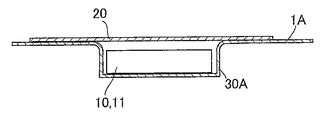
- a conventional carrier tape for electronic parts is used for a flexible resin sheet 1A wound around a take-up reel 40 and for electronic parts arranged in parallel on the resin sheet 1A.
- a storage emboss 30A which is manufactured by a manufacturer according to a predetermined molding method and then transported from the manufacturer to the component manufacturer or from the component manufacturer to the assembly manufacturer (Patent Documents 1, 2, 3, 4). 5).
- the resin sheet 1 ⁇ / b> A is formed in a long shape, and a plurality of storage embosses 30 ⁇ / b> A are arranged in parallel in the longitudinal direction at regular intervals, and a semiconductor that is an electronic component is formed on a flat surface.
- the top tape 20 that seals the package 10 is heat-sealed.
- each storage emboss 30 ⁇ / b> A is formed in a pocket shape having a predetermined depth, and functions to store the semiconductor package 10 in the peripheral wall from the opening.
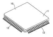
- the semiconductor package 10 As the semiconductor package 10, as shown in FIG. 11, for example, a surface mount type in which a plurality of leads 12 are juxtaposed from four directions on the peripheral surface of the package body 11 having a thickness of about 2.5 to 3.8 mm.
- QFP Quad Flat Package
- the QFP type semiconductor package 10 Since the QFP type semiconductor package 10 is surface-mounted, it has a degree of freedom of wiring on the printed circuit board, and the connection portion using solder can be clearly seen, so that it is easy to check for defects. Have.
- a carrier tape for electronic parts is manufactured by a manufacturer by a predetermined molding method
- a prepared long resin base material is preheated and set in a dedicated mold, and the resin base material is used by this mold.
- a plurality of storage embosses 30A are press-molded at regular intervals, and after the press-molded resin sheet 1A is allowed to cool for a predetermined time, the cooled resin sheet 1A is wound around the take-up reel 40 prepared, A carrier tape for electronic parts can be manufactured.
- the electronic component carrier tape wound around the take-up reel 40 is unwound and a plurality of storage embosses 30A of the unrolled resin sheet 1A are provided. If the semiconductor package 10 is sequentially stored, the top tape 20 is heat-sealed to the flat surface of the resin sheet 1A, and then the carrier tape for electronic components of a predetermined length is wound on the take-up reel 40, the electronic component The semiconductor package 10 can be stored in the carrier tape.
- the electronic component carrier tape is set for each take-up reel 40 in an automatic assembly apparatus such as a surface mounter.
- the electronic component carrier tape is fed out from the set take-up reel 40, and the top tape 20 is gradually peeled off from the surface of the resin sheet 1A.
- the semiconductor package 10 is adsorbed from the storage emboss 30A of the resin sheet 1A. If it is taken out, the semiconductor package 10 can be surface-mounted on the circuit board by soldering.
- Japanese Patent No. 4124516 Japanese Patent Laid-Open No. 2003-81331 Japanese Patent Application Laid-Open No. 2016-120961 JP 2016-120935 A JP 2015-221673 A
- the semiconductor package 10 has been further reduced in view of demands for reduction in thickness and increase in density along with the reduction in size and performance of various electronic devices. Specifically, it is designed and manufactured to a thickness of 2 mm or less, more specifically, a thickness of 1.4 to 2.0 mm.
- the conventional carrier tape for electronic components is configured to be deep and deep on the assumption that the storage emboss 30A is thick, and the thin semiconductor package 10 having a thickness of 2.0 mm or less. In general, it is not particularly important to store the thin semiconductor package 10, so that the thin semiconductor package 10 may not be properly protected.
- a thin semiconductor package 10 having a thickness of 2.0 mm or less is stored in a conventional emboss 30A for electronic component carrier tape and transported from a component manufacturer to an assembly manufacturer. Since there is a large gap between them, it may rattle out in the storage emboss 30A due to impact or vibration during transportation, and may enter between the resin sheet 1A and the top tape 20.
- the leads 12 that are thinned due to high density may be deformed and damaged, or the thin semiconductor package 10 may break the top tape 20 and fall off. is there.
- the present invention has been made in view of the above, and provides a method for manufacturing a carrier tape for electronic components that can prevent the thin electronic components from popping out of the stored embossing and being damaged or falling off even if the electronic components are thin. It is intended to provide.
- the resin sheet is press-molded by sandwiching the resin sheet between the upper mold and the lower mold of the mold so that the resin sheet has a stepped structure.
- a method of manufacturing a carrier tape for electronic parts that integrally forms the storage embossing of A plurality of flange pieces facing the resin sheet at intervals, a plurality of step walls connected to opposing portions of the plurality of flange pieces and extending from the front surface side of the flange pieces to the back surface, and the plurality of step walls Is formed from a step receiving piece which is erected between and positioned lower than the flange piece, An opening provided in the step receiving piece of the resin sheet for the storage emboss, an enclosing wall extending from the opening toward the back surface of the step receiving piece to surround the electronic component, and a bottom portion provided on the enclosing wall for mounting the electronic component And formed from When the electronic component is stored in the storage emboss, the surface of the electronic component
- the upper mold and the lower mold of the mold are overlapped in a plan view, and the overlap amount between the upper mold and the lower mold can be set to be equal to or less than the thickness of the resin sheet.
- a clearance can be formed in a plan view between the upper mold and the lower mold of the mold, and the clearance amount of this clearance can be less than the thickness of the resin sheet.
- press molding can be performed by sandwiching a preheated resin sheet between the upper mold and the lower mold of the mold.
- the upper mold and the lower mold can be press molded without applying heat to the resin sheet.
- the height from the surface of the flange piece of the resin sheet to the surface of the step receiving piece can be set to 50 ⁇ m or more and can be set to 1 ⁇ 2 or less of the thickness of the electronic component.
- the top tape is laminated and attached to the surface of the step receiving piece of the resin sheet, and the opposing portion of the top tape facing the electronic component is stored. It is also possible to make the surface close to the surface of the electronic component protruding from the opening of the emboss and to deform it.
- the electronic component can be a semiconductor package having a thickness of 2 mm or less from which a plurality of leads protrude from two or four directions on the peripheral surface of the package body.
- the resin sheet in the claims is given transparency, insulation, conductivity, and color as necessary.
- Electronic components include at least various circuit components (for example, thin capacitors, transistors, resistor elements, etc. having a thickness of 2.0 mm or less) and semiconductor packages (for example, thin BGA, SOP, SOJ, QFP having a thickness of 2.0 mm or less). , LQFP, TQFP type, etc.).
- a plurality of feed holes can be arranged in the longitudinal direction in at least one flange piece. At the bottom of the storage embossing, an attitude maintaining hole for electronic components can be provided as necessary.
- a resin sheet is press-molded to form a step structure having a height difference, and the resin sheet having the step structure and a storage emboss are formed. Is then integrated into a carrier tape for electronic components, and then the electronic components are stored in the embossing of the electronic component carrier tape, and the top tape is applied to the step receiving piece positioned lower than the flange piece of the resin sheet. What is necessary is just to laminate and stick.
- the facing portion facing the electronic component of the top tape is in close contact with the surface of the protruding portion of the electronic component protruding from the storage emboss, and this close portion is deformed according to the shape of the protruding portion of the electronic component.
- the electronic component is positioned in the XY direction by the rising of the deformed and raised inclined portion of the close proximity to the peripheral surface of the protruding portion of the electronic component.
- the opposing portion of the top tape does not face the surface of the electronic component with a large gap, but rather closes the electronic component close to the surface of the electronic component with almost no gap, thereby holding the electronic component in the Z direction. Position.
- the top tape can be brought into close contact with the electronic component to restrict the movement of the electronic component. Therefore, even if the electronic component is thin, the thin electronic component jumps out of the embossing of the resin sheet and is damaged. Or effectively falling off. Moreover, since the carrier tape for electronic components is manufactured by the press molding method, high reproducibility and dimensional accuracy can be obtained.
- the resin sheet is prevented from being deformed and damaged, and a plurality of resin sheets It is easy to form the flange piece and the step receiving piece in a step structure and provide a height difference therebetween.
- the clearance amount of the mold clearance is less than the thickness of the resin sheet, it is effective that the end of the resin sheet jumps up during the press molding of the resin sheet and the molding defect occurs. Can be prevented.
- the preheated resin sheet is press-molded to produce the electronic component carrier tape, it is possible to avoid the occurrence of warpage and sink marks. Therefore, remarkable improvement in workability and moldability can be expected, and extremely high reproducibility and dimensional accuracy can be obtained.
- the height from the surface of the flange piece of the resin sheet to the surface of the step receiving piece is 50 ⁇ m or more and 1/2 or less of the thickness of the electronic component, It is possible to reduce the possibility that the holding may be hindered or the electronic component may jump out. In addition, the electronic component can be easily held in the storage emboss.
- the facing portion of the top tape is covered with the surface of the protruding portion of the electronic component protruding from the opening of the storage emboss so as to be in close contact, and the contacting portion of the top tape is deformed. Swelling and the sloped portion of the raised close contact portion are close to the peripheral surface of the protruding portion of the electronic component, and thus the electronic component can be appropriately positioned. Further, since the close portion of the top tape is in close contact with the surface of the electronic component with almost no gap, the electronic component can be appropriately positioned in the height direction.
- the seventh aspect of the present invention even if the semiconductor package is thin, it is possible to effectively prevent a thin semiconductor package having a thickness of 2 mm or less from jumping out of the storage emboss and being damaged or falling off.
- FIG. 10 is a cross-sectional explanatory view of FIG. 9. It is a perspective explanatory view showing a QFP type semiconductor package.
- a manufacturing method of a carrier tape for an electronic component includes a mold as shown in FIGS. 1 to 6, 8, and 11. 51.
- the resin sheet 1 is sandwiched between the upper mold 52 and the lower mold 53 and press-molded to form the resin sheet 1 in a step structure with a height difference, and the resin sheet 1 is accommodated for a thin semiconductor package 10.
- the emboss 30 is integrally formed, when the thin semiconductor package 10 is stored in the storage emboss 30, the surface 13 of the thin semiconductor package 10 is positioned higher than the step receiving piece 6 of the resin sheet 1, and the resin sheet 1 is positioned lower than the surface of the flange piece 2.
- the resin sheet 1 supports a plurality of storage embosses 30 interposed between a pair of left and right flange pieces 2 facing each other with a space therebetween, and the pair of left and right flange pieces 2.
- the step receiving piece 6 is integrally formed with a long flexible strip, and is wound around the take-up reel 40.
- the material of the resin sheet 1 is not particularly limited, but transparent polystyrene having excellent versatility, A-PET, polyethylene terephthalate having excellent strength, polypropylene having excellent chemical resistance, mechanical properties and moldability. Examples include base materials such as excellent ABS resin and polycarbonate excellent in impact resistance and dimensional stability.
- the width of the resin sheet 1 is set to a standardized size such as 12, 16, 24, 32, 44, 56, 72 mm, for example.
- the thickness of the resin sheet 1 is not particularly limited, but is 0.17 to 0.50 mm, preferably 0.25 to 0.40 mm, more preferably from the viewpoint of achieving both flexibility and strength. The thickness is about 0.30 mm.
- each of the pair of flange pieces 2 is formed in an elongated band shape, and a plurality of feed holes 3 for feeding out the carrier tape for electronic parts are provided in the longitudinal direction of the outer side of at least one of the flange pieces 2.
- the holes are drilled side by side at a predetermined interval.
- the inner side which a pair of flange piece 2 opposes in other words, as shown in FIG.1 and FIG.2, the opposing part 4 hangs down from the surface side of the flange piece 2 to the back surface direction (downward direction of FIG. 2).
- the stepped walls 5 extending in this manner are connected to each other, and between the lower ends of the pair of stepped walls 5, a step receiving piece 6 positioned lower than the flange piece 2 is horizontally installed.
- a flexible top tape 20 that covers and protects the thin semiconductor package 10 from above is heat-sealed to the surface of the substrate.
- Each step wall 5 is formed in a substantially I-shaped cross section and has a height of 50 ⁇ m or more, in other words, a height of the top tape 20 or more. Therefore, when the thickness of the top tape 20 is 50 ⁇ m or more, the height is set to 50 ⁇ m or more, and when the thickness of the top tape 20 is 70 ⁇ m or more, the height is set to 70 ⁇ m or more.
- the step receiving piece 6 is formed in an elongated flat plate shape extending in the longitudinal direction of the flange piece 2 (vertical direction in FIG. 1), and a plurality of storage embosses 30 are arranged in the longitudinal direction at predetermined intervals.
- the height h from the surface of the pair of flange pieces 2 positioned at the high level to the surface of the step receiving piece 6 positioned at the low level is set to 50 ⁇ m or more and 1/2 or less of the thickness of the thin semiconductor package 10. The This is because when the thickness is less than 50 ⁇ m, the thickness is equal to or less than the thickness of the top tape 20, and the holding of the thin semiconductor package 10 may be hindered and may jump out. On the other hand, if the thickness of the thin semiconductor package 10 exceeds 1 ⁇ 2, it is difficult to hold the thin semiconductor package 10 in the storage emboss 30 and the thin semiconductor package 10 may jump out.
- the thin semiconductor package 10 is made of, for example, a surface mount type QFP type.
- the thin semiconductor package 10 includes a package body 11 made of a resin mold and having a substantially rectangular plane, and a plurality of leads 12 project side by side from the four directions of the peripheral surface of the package body 11, and each lead 12 has a gull wing shape ( It is bent thinly into a substantially L shape.
- the package body 11 is designed and manufactured to have a thickness (height) of 2 mm or less, specifically, a thickness of 1.4 to 2.0 mm in view of the demand for thinning, and becomes the thickness of the semiconductor package 10. .
- the surface 13 of the package body 11 becomes the upper surface of the thin semiconductor package 10, in other words, the surface 13 of the thin semiconductor package 10.
- Such a thin semiconductor package 10 is taken out of the storage emboss 30 by the automatic assembly device after the carrier tape for electronic parts is set together with the take-up reel 40 and mounted on the surface of the circuit board by soldering.
- the top tape 20 is not particularly limited.
- the top tape 20 may be bonded to a base material such as a polyester film, a polyethylene terephthalate film, or a polyethylene film, and a pressure-sensitive adhesive layer or a heat-fusible adhesive having room temperature adhesion.
- a type in which a pressure-sensitive adhesive layer is laminated is used.
- the top tape 20 is composed of a conductive type, an antistatic type, a transparent type, etc., and has a thickness of about 50 to 70 ⁇ m, preferably about 55 to 65 ⁇ m, more preferably about 56 to 60 ⁇ m.
- the storage emboss 30 extends from the peripheral edge of each opening 31 while being inclined toward the back surface of the step receiving piece 6. And an enclosure wall 32 that surrounds the semiconductor package 10 and a bottom 33 that is provided at the lower end of each enclosure wall 32 and on which the semiconductor package 10 is mounted. It is integrated with the resin sheet 1.
- each opening 31 is formed in a planar rectangle, specifically a square, with a size capable of accommodating the thin semiconductor package 10.
- the surrounding wall 32 is formed in a hollow, substantially truncated pyramid shape that gradually narrows downward, and functions to contact and position the plurality of leads 12 of the thin semiconductor package 10. .
- the height of the surrounding wall 32 is positioned such that the surface 13 of the package body 11 is slightly higher than the step receiving piece 6 and slightly lower than the surfaces of the pair of flange pieces 2 when the thin semiconductor package 10 is stored. It is set as follows.
- the bottom 33 is formed in a flat rectangular shape, and a round posture maintaining hole 34 is drilled through the center as necessary.
- the posture maintaining hole 34 functions to exhaust air from the inside of the storage emboss 30 to the outside based on driving of a vacuum device such as a vacuum pump, and appropriately maintain the posture of the thin semiconductor package 10.
- a vacuum device such as a vacuum pump
- it is also used when detecting the presence or absence of the thin semiconductor package 10 by a detection sensor.
- the take-up reel 40 is standardized to a predetermined size according to the application, and the resin sheet 1 is record-wound in one row, or traverse-wound in a plurality of rows, so that an inspection device or an automatic assembly device (for example, a surface) (See FIG. 8).
- the take-up reel 40 includes a general-purpose resin-made normal take-up reel excellent in versatility, a conductive take-up reel in which carbon or the like is blended, an anti-static take-up reel in which an anti-static effect is applied to the normal take-up reel, There are various types such as a lightweight foam core take-up reel, but it is not particularly limited as long as it can be set in an inspection device, an automatic assembly device or the like.
- a flat and long resin sheet 1 for processing into a carrier tape for electronic parts is prepared. At this time, it is preferable to form the resin sheet 1 in a band shape having a predetermined width. After preparing the resin sheet 1 for processing, the resin sheet 1 is heated and softened by a heater or the like and set in a die 51 of a dedicated press molding apparatus 50 that can obtain high reproducibility and dimensional accuracy. The preheated resin sheet 1 is pressed to be deformed into a step structure, whereby a carrier tape for electronic parts having a height difference between the pair of flange pieces 2 and the step receiving piece 6 is press-molded.
- the mold 51 of the press molding apparatus 50 includes a movable upper mold 52 that holds the resin sheet 1 in the vertical direction and a fixed lower mold 53.
- the mold 53 is opposed so as to be slightly overlapped in plan view, and the overlap amount ol between the upper mold 52 and the lower mold 53 is set to be equal to or less than the thickness of the resin sheet 1. This is because when the overlap amount ol between the upper mold 52 and the lower mold 53 exceeds the thickness of the resin sheet 1, the resin sheet 1 is cut without being deformed, and it is difficult to bend the carrier tape for electronic parts. Because it becomes.
- a plurality of punching pins that are punches and holes that are dies are arranged on the mold 51 so as to face each other.
- the plurality of punching pins and the holes punch a plurality of feed holes 3 that are recesses in the longitudinal direction of at least one side of the pair of flange pieces 2 of the resin sheet 1 at a predetermined interval.
- the upper mold 52 When the upper mold 52 is clamped to the lower mold 53 of the mold 51 and the already preheated resin sheet 1 is press-molded, the upper mold 52 and the lower mold 53 of the mold 51 are heated to further heat the resin sheet 1. However, if the cavities of the upper mold 52 and the lower mold 53 are not heated to a room temperature or lower, and plastic processing is performed without further heating the resin sheet 1, the resin sheet 1 may be recessed during molding. Deformation of a plurality of feed holes 3 can be reliably prevented.
- the electronic component carrier tape When the electronic component carrier tape is press-molded, the electronic component carrier tape can be manufactured by winding the electronic component carrier tape on the prepared take-up reel 40.
- the thin semiconductor package 10 is stored in the manufactured electronic component carrier tape, the electronic component carrier tape wound around the take-up reel 40 is unwound, and a plurality of the storage embosses of the unrolled resin sheet 1 are stored.
- the thin semiconductor package 10 is sequentially stored in 30, and then the top tape 20 is laminated on the surface of the step receiving piece 6 of the resin sheet 1 and heat-sealed.
- the opposing portion 21 that opposes the thin semiconductor package 10 of the top tape 20 has a thin semiconductor package 10 package from the opening 31 of the storage emboss 30 as shown in FIGS. Since the surface 13 of the main body 11 protrudes slightly, the surface 13 of the package main body 11 protruding slightly is covered closely.
- the facing portion 21 of the top tape 20 facing the thin semiconductor package 10 becomes a close contact portion that is in close contact with the surface 13 of the package body 11, and the close contact portion is deformed to bulge and form a substantially trapezoidal cross section.
- the protruding inclined portion 22 of the close contact portion approaches the upper peripheral surface 14 of the package body 11 from the XY direction
- the thin semiconductor package 10 is positioned in the XY direction.
- the facing portion 21 that opposes the thin semiconductor package 10 of the top tape 20 does not face the surface 13 of the package main body 11 with a gap, but is in close contact with the surface 13 of the package main body 11 as a close portion without any gap,
- the thin semiconductor package 10 is also positioned in the Z direction by being reduced.
- the step receiving piece 6 is positioned lower than the pair of flange pieces 2 of the resin sheet 1, it is possible to effectively eliminate the possibility that the thin semiconductor package 10 is displaced in the XY direction or the thin semiconductor package 10 jumps out. be able to. This is because when the step receiving piece 6 is positioned at the same position as the pair of flange pieces 2 or higher than the pair of flange pieces 2, the top tape 20 contacts the surface 13 of the thin semiconductor package 10. This is because the thin semiconductor package 10 may be displaced in the XY direction or the thin semiconductor package 10 may jump out.
- the electronic component carrier tape is wound on the take-up reel 40 by winding a predetermined length of the electronic component carrier tape.
- a thin semiconductor package 10 can be accommodated.
- the top tape 20 is always kept in close contact with the thin semiconductor package 10 having a thickness of 2.0 mm or less to restrict the movement of the thin semiconductor package 10 in the XYZ directions. Even if vibrations or the like are applied, the thin semiconductor package 10 sticks out in the storage emboss 30 and does not protrude between the resin sheet 1 and the top tape 20. Therefore, the thin lead 12 of the thin semiconductor package 10 is deformed and damaged, the thin semiconductor package 10 slips between the resin sheet 1 and the top tape 20 and falls outside, or breaks the top tape 20 and falls off. Can be effectively prevented.
- the carrier tape for electronic parts is press-molded, it can be easily applied to the production of a thin, light and small carrier tape for electronic parts, and there is little loss of material, and a great improvement in productivity can be expected. Furthermore, even when the resin sheet 1 is a composite material with poor elongation that cannot be formed by vacuum forming or pressure forming, a carrier tape for electronic parts can be easily formed.
- FIG. 7 shows a second embodiment of the present invention.
- a clearance is defined, and the clearance amount c of the clearance is set to be less than the thickness of the resin sheet 1.
- the other parts are the same as those in the above embodiment, and the description thereof is omitted.
- the same effect as the above embodiment can be expected, and furthermore, since the clearance amount c between the upper mold 52 and the lower mold 53 is less than the thickness of the resin sheet 1, the stress is dispersed during press molding. There is no invitation. Therefore, it is clear that it is possible to effectively prevent the end of the resin sheet 1 from bouncing and forming defects during press molding of the resin sheet 1.
- a plurality of feed holes 3 for feeding out the carrier tape for electronic parts may be previously drilled at a predetermined interval.
- the step wall 5 of the resin sheet 1 is a vertical wall, but the step wall 5 may be inclined inward.
- the thin semiconductor package 10 was made into QFP type, the surface mounting type
- SOP Small Outline Package
- the surrounding wall 32 of the storage emboss 30 can be formed into a rectangular tubular surrounding wall 32 without being inclined.
- a flat rectangular raised bottom on which the package body 11 of the thin semiconductor package 10 is mounted is formed on the bottom surface of the storage emboss 30 so as to protrude thinly on the surface peripheral portion of the raised bottom.
- Positioning ribs straddling a plurality of leads 12 of the semiconductor package 10 are formed so as to protrude, and the thin semiconductor package 10 can be positioned with high accuracy in the XY directions by using the positioning ribs.
- the method for manufacturing a carrier tape for electronic parts according to the present invention is used in the field of manufacturing semiconductors, portable devices, information devices, precision devices and the like.
Landscapes
- Engineering & Computer Science (AREA)
- Mechanical Engineering (AREA)
- Packaging Frangible Articles (AREA)
- Packages (AREA)
Abstract
本発明は、樹脂シート(1)をプレス成形することにより、段差構造の樹脂シート(1)に半導体パッケージ(10)用の収納エンボス(30)を一体形成する製法であり、樹脂シート(1)を、対向する複数のフランジ片(2)と、複数のフランジ片(2)の対向部(4)に接続されてフランジ片(2)の裏面方向に伸びる複数の段差壁(5)と、複数の段差壁(5)間に架設されてフランジ片(2)よりも低位に位置する段差受片(6)とから形成し、収納エンボス(30)を、段差受片(6)に設けられる開口(31)と、開口(31)から段差受片(6)の裏面方向に伸びる包囲壁(32)と、包囲壁(32)に設けられる底部(33)とから形成し、収納エンボス(30)に半導体パッケージ(10)を収納する場合、半導体パッケージ(10)の表面(13)を段差受片(6)よりも高く位置させ、フランジ片(2)の表面よりも低く位置させる電子部品用キャリアテープの製造方法であり、収納エンボスから薄い電子部品が飛び出して損傷したり、脱落することを防止する。
Description
本発明は、半導体パッケージ等からなる電子部品の収納、供給、保管、在庫管理、輸送等に用いられる電子部品用キャリアテープの製造方法に関するものである。
従来における電子部品用キャリアテープは、図8ないし図11に示すように、巻取りリール40に巻回される可撓性の樹脂シート1Aと、この樹脂シート1Aに並設される電子部品用の収納エンボス30Aとを備え、製造メーカで所定の成形法により製造された後、製造メーカから部品メーカに輸送されたり、あるいは部品メーカからアッセンブリメーカに輸送される(特許文献1、2、3、4、5参照)。
樹脂シート1Aは、図9や図10に示すように、長尺に形成されてその長手方向に複数の収納エンボス30Aが一定の間隔で並設され、平坦な表面には、電子部品である半導体パッケージ10を封止するトップテープ20が加熱融着される。各収納エンボス30Aは、図10に示すように、所定の深さのポケット形に形成され、開口から周壁内に半導体パッケージ10を収納するよう機能する。
半導体パッケージ10としては、図11に示すように、例えば2.5~3.8mm程度の厚さを有するパッケージ本体11の周面四方向から複数本のリード12が並んで突出する表面実装型のQFP(Quad Flat Package)タイプがあげられる。このQFPタイプの半導体パッケージ10は、表面実装のため、プリント基板の配線の自由度が得られ、しかも、ハンダを用いた接続部分が明瞭に視認できるので、不良の確認が容易であるという特徴を有している。
このような電子部品用キャリアテープを製造メーカが所定の成形法により製造する場合には、用意した長尺の樹脂基材を予熱して専用の金型にセットし、この金型により樹脂基材に複数の収納エンボス30Aを一定の間隔でプレス成形し、このプレス成形した樹脂シート1Aを所定の時間放置して冷却した後、冷却した樹脂シート1Aを用意した巻取りリール40に巻き取れば、電子部品用キャリアテープを製造することができる。
製造された電子部品用キャリアテープに半導体パッケージ10を部品メーカが収納する場合には、巻取りリール40に巻回された電子部品用キャリアテープを繰り出し、繰り出した樹脂シート1Aの複数の収納エンボス30Aに半導体パッケージ10を順次収納し、樹脂シート1Aの平坦な表面にトップテープ20を加熱融着した後、巻取りリール40に所定の長さの電子部品用キャリアテープを巻き取れば、電子部品用キャリアテープに半導体パッケージ10を収納することができる。
次に、電子部品用キャリアテープに収納された半導体パッケージ10をアッセンブリメーカが回路基板に実装する場合には、表面実装機等の自動組立装置に電子部品用キャリアテープを巻取りリール40毎セットし、このセットした巻取りリール40から電子部品用キャリアテープを繰り出すとともに、樹脂シート1Aの表面からトップテープ20を徐々に剥離し、その後、樹脂シート1Aの収納エンボス30Aから半導体パッケージ10を吸着して取り出せば、回路基板に半導体パッケージ10をハンダにより表面実装することが可能となる。
ところで、近年の半導体パッケージ10は、様々な電子機器の小型化や高性能化に伴い、薄型化や高密度化の要求が急速に高まっているのに鑑み、さらなる薄型化が図られている。具体的には2mm以下の厚さ、より具体的には1.4~2.0mmの厚さに設計され、製造されている。
このような半導体パッケージ10の薄型化が図られる場合、従来の電子部品用キャリアテープは、収納エンボス30Aが厚い半導体パッケージ10を前提に大きく深く構成され、厚さ2.0mm以下の薄い半導体パッケージ10の収納を特に重視していないのが一般的であるので、薄い半導体パッケージ10を適切に保護できなくなるおそれがある。
この点について説明すると、厚さ2.0mm以下の薄い半導体パッケージ10は、従来の電子部品用キャリアテープの収納エンボス30Aに収納され、部品メーカからアッセンブリメーカに輸送される場合、トップテープ20との間に大きな隙間が存在するので、輸送時の衝撃や振動等により、収納エンボス30A内でがたついて飛び出し、樹脂シート1Aとトップテープ20の間に侵入することがある。薄い半導体パッケージ10が樹脂シート1Aとトップテープ20の間に侵入すると、高密度化で細くなったリード12が変形して損傷したり、薄い半導体パッケージ10がトップテープ20を破って脱落することがある。
本発明は上記に鑑みなされたもので、例え電子部品が薄くても、収納エンボスから薄い電子部品が飛び出して損傷したり、脱落するのを防止することのできる電子部品用キャリアテープの製造方法を提供することを目的としている。
本発明においては上記課題を解決するため、金型の上型と下型との間に樹脂シートを挟んでプレス成形することにより、樹脂シートを段差構造に構成し、この樹脂シートに電子部品用の収納エンボスを一体形成する電子部品用キャリアテープの製造方法であって、
樹脂シートを、間隔をおいて対向する複数のフランジ片と、この複数のフランジ片の対向部にそれぞれ接続されてフランジ片の表面側から裏面方向に伸びる複数の段差壁と、この複数の段差壁の間に架設されてフランジ片よりも低位に位置する段差受片とから形成し、
収納エンボスを、樹脂シートの段差受片に設けられる開口と、この開口から段差受片の裏面方向に伸びて電子部品を包囲する包囲壁と、この包囲壁に設けられて電子部品を搭載する底部とから形成し、
収納エンボスに電子部品を収納する場合に、電子部品の表面を樹脂シートの段差受片よりも高く位置させるとともに、樹脂シートのフランジ片の表面よりも低く位置させることを特徴としている。
樹脂シートを、間隔をおいて対向する複数のフランジ片と、この複数のフランジ片の対向部にそれぞれ接続されてフランジ片の表面側から裏面方向に伸びる複数の段差壁と、この複数の段差壁の間に架設されてフランジ片よりも低位に位置する段差受片とから形成し、
収納エンボスを、樹脂シートの段差受片に設けられる開口と、この開口から段差受片の裏面方向に伸びて電子部品を包囲する包囲壁と、この包囲壁に設けられて電子部品を搭載する底部とから形成し、
収納エンボスに電子部品を収納する場合に、電子部品の表面を樹脂シートの段差受片よりも高く位置させるとともに、樹脂シートのフランジ片の表面よりも低く位置させることを特徴としている。
なお、金型の上型と下型とを平面視でオーバーラップさせ、上型と下型とのオーバーラップ量を樹脂シートの厚さ以下とすることができる。
また、金型の上型と下型との間に平面視でクリアランスを形成し、このクリアランスのクリアランス量を樹脂シートの厚さ未満とすることができる。
また、金型の上型と下型との間に予備加熱した樹脂シートを挟んでプレス成形することもできる。
また、金型の上型と下型との間に平面視でクリアランスを形成し、このクリアランスのクリアランス量を樹脂シートの厚さ未満とすることができる。
また、金型の上型と下型との間に予備加熱した樹脂シートを挟んでプレス成形することもできる。
また、金型の上型と下型との間に樹脂シートを挟んでプレス成形する際、上型と下型により、樹脂シートに熱を加えることなくプレス成形することが可能である。
また、樹脂シートのフランジ片の表面から段差受片の表面までの高さを、50μm以上とするとともに、電子部品の厚さの1/2以下とすることが可能である。
また、樹脂シートのフランジ片の表面から段差受片の表面までの高さを、50μm以上とするとともに、電子部品の厚さの1/2以下とすることが可能である。
また、樹脂シートに一体形成した収納エンボスに電子部品を収納した後、樹脂シートの段差受片の表面にトップテープを積層して貼り着け、このトップテープの電子部品に対向する対向部を、収納エンボスの開口から突出した電子部品の表面に密接させ、変形させることも可能である。
また、電子部品を、パッケージ本体の周面の二方向あるいは四方向から複数本のリードが突出する厚さ2mm以下の半導体パッケージとすることができる。
また、電子部品を、パッケージ本体の周面の二方向あるいは四方向から複数本のリードが突出する厚さ2mm以下の半導体パッケージとすることができる。
ここで、特許請求の範囲における樹脂シートは、必要に応じて透明性、絶縁性、導電性、色彩が付与される。電子部品には、少なくとも各種の回路部品(例えば、厚さ2.0mm以下の薄いキャパシタ、トランジスタ、抵抗素子等)や半導体パッケージ(例えば、厚さ2.0mm以下の薄いBGA、SOP、SOJ、QFP、LQFP、TQFPタイプ等)が含まれる。また、樹脂シートの複数のフランジ片のうち、少なくとも一のフランジ片には、複数の送り孔を長手方向に並べ設けることができる。収納エンボスの底部には、必要に応じ、電子部品用の姿勢維持孔を設けることができる。
本発明によれば、電子部品用キャリアテープに電子部品を収納する場合には、先ず、樹脂シートをプレス成形して高低差を有する段差構造に構成するとともに、この段差構造の樹脂シートと収納エンボスとを一体化して電子部品用キャリアテープを製造し、その後、電子部品用キャリアテープの収納エンボス内に電子部品を収納し、樹脂シートのフランジ片よりも低位に位置する段差受片にトップテープを積層して貼り着ければ良い。
すると、トップテープの電子部品に対向する対向部は、収納エンボスから突出している電子部品の突出部の表面に密接して密接部となり、この密接部が電子部品の突出部の形状に応じて変形しながら盛り上がり、この変形して盛り上がった密接部の傾斜部分が電子部品の突出部の周面に近接することにより、電子部品をXY方向に位置決めする。また、トップテープの対向部は、電子部品の表面に大きな隙間をおいて対向するのではなく、電子部品の表面に略隙間なく密接して電子部品を抑え込むことにより、電子部品をZ方向にも位置決めする。
本発明によれば、電子部品にトップテープを密接させて電子部品の動きを規制することができるので、例え電子部品が薄くても、薄型の電子部品が樹脂シートの収納エンボスから飛び出して損傷したり、脱落するのを有効に防止することができるという効果がある。また、プレス成形法により電子部品用キャリアテープを製造するので、高い再現性や寸法精度を得ることができる。
請求項2記載の発明によれば、金型の上型と下型のオーバーラップ量を樹脂シートの厚さ以下とするので、樹脂シートが変形して損傷するのを防止し、樹脂シートの複数のフランジ片と段差受片とを段差構造に形成してこれらの間に高低差を設けることが容易となる。
請求項3記載の発明によれば、金型のクリアランスのクリアランス量を樹脂シートの厚さ未満とするので、樹脂シートのプレス成形時に樹脂シートの端部等が跳ね上がり、成形不良が生じるのを有効に防止することができる。
請求項3記載の発明によれば、金型のクリアランスのクリアランス量を樹脂シートの厚さ未満とするので、樹脂シートのプレス成形時に樹脂シートの端部等が跳ね上がり、成形不良が生じるのを有効に防止することができる。
請求項4記載の発明によれば、予備加熱した樹脂シートをプレス成形して電子部品用キャリアテープを製造するので、反りやヒケの発生を回避することができる。したがって、加工性や成形性の著しい向上が期待でき、しかも、きわめて高い再現性や寸法精度を得ることが可能になる。
請求項5記載の発明によれば、樹脂シートのフランジ片の表面から段差受片の表面までの高さを、50μm以上、かつ電子部品の厚さの1/2以下とするので、電子部品の保持に支障を来したり、電子部品が飛び出すおそれを低減することが可能になる。また、収納エンボス内における電子部品の保持が容易となる。
請求項5記載の発明によれば、樹脂シートのフランジ片の表面から段差受片の表面までの高さを、50μm以上、かつ電子部品の厚さの1/2以下とするので、電子部品の保持に支障を来したり、電子部品が飛び出すおそれを低減することが可能になる。また、収納エンボス内における電子部品の保持が容易となる。
請求項6記載の発明によれば、収納エンボスの開口から突出している電子部品の突出部の表面にトップテープの対向部が密接被覆して密接部となり、このトップテープの密接部が変形して盛り上がり、この盛り上がった密接部の傾斜部分が電子部品の突出部周面に近接するので、電子部品を適切に位置決めすることが可能になる。また、トップテープの密接部が電子部品の表面に略隙間なく密接するので、電子部品を高さ方向にも適切に位置決めすることが可能になる。
請求項7記載の発明によれば、例え半導体パッケージが薄くても、厚さ2mm以下の薄い半導体パッケージが収納エンボスから飛び出して損傷したり、脱落するのを有効に防止することが可能になる。
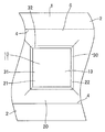
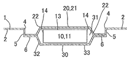
以下、図面を参照して本発明の好ましい実施の形態を説明すると、本実施形態における電子部品用キャリアテープの製造方法は、図1ないし図6、図8、図11に示すように、金型51の上型52と下型53に樹脂シート1を挟持させてプレス成形することにより、樹脂シート1を高低差付きの段差構造に構成するとともに、この樹脂シート1に薄い半導体パッケージ10用の収納エンボス30を一体形成する製造方法であり、収納エンボス30に薄い半導体パッケージ10を収納した場合に、薄い半導体パッケージ10の表面13を樹脂シート1の段差受片6よりも高く位置させ、かつ樹脂シート1のフランジ片2の表面よりも低く位置させるようにしている。
樹脂シート1は、図1や図2に示すように、間隔をおいて相対向する左右一対のフランジ片2と、この左右一対のフランジ片2の間に介在されて複数の収納エンボス30を支持する段差受片6とを一体に備えた可撓性の長い帯形に形成され、巻取りリール40に巻回される。この樹脂シート1の材料としては、特に限定されるものではないが、汎用性に優れる透明のポリスチレン、A‐PET、強度に優れるポリエチレンテレフタレート、耐薬品性に優れるポリプロピレン、機械的性質や成形性に優れるABS樹脂、耐衝撃性や寸法安定性に優れるポリカーボネート等の基材があげられる。
樹脂シート1は、空気中に放電して静電気を帯びないようにする場合には、ポリスチレン等に帯電防止効果が施された帯電防止タイプが使用される。また、静電気の発生を防止したい場合には、ポリスチレンやA‐PET等にカーボン等が配合された導電タイプが使用される。樹脂シート1の幅は、例えば規格化された12、16、24、32、44、56、72mm等のサイズに設定される。樹脂シート1の厚さは、特に限定されるものではないが、可撓性と強度とを両立させる観点から、0.17~0.50mm、好ましくは0.25~0.40mm、より好ましくは0.30mm前後の薄さとされる。
一対のフランジ片2は、図1に示すように、それぞれ細長い帯形に形成され、少なくとも一方のフランジ片2の外側部長手方向に、電子部品用キャリアテープを繰り出すための複数の送り孔3が所定の間隔をおき並べて穿孔される。また、一対のフランジ片2の対向する内側部、換言すれば、対向部4には図1や図2に示すように、フランジ片2の表面側から裏面方向(図2の下方向)に垂下して伸びる段差壁5がそれぞれ接続され、この一対の段差壁5の下端部間には、フランジ片2よりも低位に位置する段差受片6が水平に架設されており、この段差受片6の表面には、薄い半導体パッケージ10を上方から被覆保護する可撓性のトップテープ20が加熱融着される。
各段差壁5は、断面略I字形に形成され、50μm以上の高さ、換言すれば、トップテープ20の厚さ以上の高さとされる。したがって、トップテープ20の厚さが50μm以上の場合には、50μm以上の高さに設定され、トップテープ20の厚さが70μm以上の場合には、70μm以上の高さに設定される。また、段差受片6は、フランジ片2の長手方向(図1の上下方向)に伸びる細長い平坦な板形に形成され、長手方向に複数の収納エンボス30が所定の間隔をおいて配列形成される。
高位に位置する一対のフランジ片2の表面から低位に位置する段差受片6の表面までの高さhは、50μm以上とされるとともに、薄い半導体パッケージ10の厚さの1/2以下とされる。これは、50μm未満の場合には、トップテープ20の厚み以下となり、薄い半導体パッケージ10の保持に支障を来して飛び出しのおそれがあるからである。これに対し、薄い半導体パッケージ10の厚さの1/2を越える場合には、収納エンボス30内における薄い半導体パッケージ10の保持が困難となり、薄い半導体パッケージ10が飛び出すおそれがあるからである。
薄い半導体パッケージ10は、図11に示すように、例えば表面実装型のQFPタイプからなる。この薄い半導体パッケージ10は、樹脂モールド製で平面略矩形のパッケージ本体11を備え、このパッケージ本体11の周面四方向から複数本のリード12が並んで突出しており、各リード12がガルウイング形(略L字形)に細く屈曲形成される。パッケージ本体11は、薄型化の要請に鑑み、2mm以下の厚さ(高さ)、具体的には1.4~2.0mmの厚さに設計され、製造され、半導体パッケージ10の厚さとなる。このパッケージ本体11の表面13は、薄い半導体パッケージ10の上面、換言すれば、薄い半導体パッケージ10の表面13となる。
このような薄い半導体パッケージ10は、電子部品用キャリアテープが巻取りリール40と共に自動組立装置にセットされた後、この自動組立装置により、収納エンボス30から取り出され、回路基板にハンダで表面実装される。
トップテープ20は、図4に示すように、特に限定されるものではないが、例えばポリエステルフィルム、ポリエチレンテレフタレートフィルム、ポリエチレンフィルム等の基材に、常温接着性の感圧式粘着層や熱融着性の感圧式粘着層が積層されたタイプが用いられる。このトップテープ20は、導電タイプ、帯電防止タイプ、透明タイプ等からなり、50~70μm、好ましくは55~65μm、より好ましくは56~60μm程度の厚さとされる。
収納エンボス30は、図2に示すように、段差受片6に所定の間隔で並べて穿孔される複数の開口31と、各開口31の周縁部から段差受片6の裏面方向に傾斜しながら伸びて半導体パッケージ10を包囲する包囲壁32と、各包囲壁32の下端部に設けられて半導体パッケージ10を搭載する底部33とを備え、厚さ2.0mm以下の薄い半導体パッケージ10の収納を前提に樹脂シート1に一体化される。
各開口31は、図1に示すように、薄い半導体パッケージ10を収納可能な大きさの平面矩形、具体的には正方形に形成される。また、包囲壁32は、図2に示すように、下方に向かうにしたがい徐々に狭まる中空の略角錐台形に形成され、薄い半導体パッケージ10の複数本のリード12に接触して位置決めするよう機能する。この包囲壁32の高さは、薄い半導体パッケージ10の収納時にパッケージ本体11の表面13が段差受片6よりも僅かに高く位置するとともに、一対のフランジ片2の表面よりも僅かに低く位置するよう設定される。
底部33は、同図に示すように、平面矩形に形成され、必要に応じ、中央に丸い姿勢維持孔34が貫通して穿孔される。この姿勢維持孔34は、真空ポンプ等のバキューム装置の駆動に基づいてエアを収納エンボス30の内部から外部に排気し、薄い半導体パッケージ10の姿勢を適切に維持するよう機能する。また、薄い半導体パッケージ10の姿勢維持の他、検出センサにより、薄い半導体パッケージ10の有無を検出する場合にも利用される。
巻取りリール40は、用途に応じた所定の大きさに規格化され、樹脂シート1が一列にレコード巻きされたり、あるいは複数列にトラバース巻きされたりして検査装置や自動組立装置(例えば、表面実装機)等にセットされる(図8参照)。この巻取りリール40には、汎用性に優れる汎用樹脂製のノーマル巻取りリール、カーボン等が配合された導電巻取りリール、ノーマル巻取りリールに帯電防止効果が施された帯電防止巻取りリール、軽量の発泡芯巻取りリール等の種類があるが、検査装置や自動組立装置等にセット可能であれば、特に限定されるものではない。
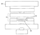
上記構成において、電子部品用キャリアテープを製造する場合には、先ず、電子部品用キャリアテープに加工するための平坦な長尺の樹脂シート1を用意する。この際、樹脂シート1を所定の幅の帯形に形成しておくことが好ましい。加工用の樹脂シート1を用意したら、この樹脂シート1をヒータ等により加熱軟化させて高い再現性や寸法精度が得られる専用のプレス成形装置50の金型51にセットし、この金型51により予備加熱した樹脂シート1をプレスして段差構造に変形させることにより、一対のフランジ片2と段差受片6との間に高低差を有する電子部品用キャリアテープをプレス成形する。
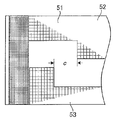
プレス成形装置50の金型51は、図5や図6に示すように、樹脂シート1を上下方向から挟持する可動の上型52と固定の下型53とを備え、これら上型52と下型53とが平面視で僅かにオーバーラップするよう接離可能に対設されており、上型52と下型53とのオーバーラップ量olが樹脂シート1の厚さ以下に設定される。これは、上型52と下型53とのオーバーラップ量olが樹脂シート1の厚さを越える場合には、樹脂シート1が変形せずに切断し、電子部品用キャリアテープの屈曲成形が困難になるからである。
また、金型51には、パンチである複数の打ち抜きピンと、ダイである穴部とが相対向するよう配設される。これら複数の打ち抜きピンと穴部とは、樹脂シート1の一対のフランジ片2の両側部のうち、少なくとも一側部の長手方向に凹部である複数の送り孔3を所定の間隔で穿孔する。
金型51の下型53に上型52を型締めして既に予備加熱した樹脂シート1をプレス成形する際、金型51の上型52と下型53を加熱して樹脂シート1にさらに熱を加えても良いが、上型52と下型53のキャビティを加熱せずに常温以下とし、樹脂シート1にさらに熱を加えることなく、塑性加工すれば、樹脂シート1の成形中に凹部である複数の送り孔3の変形を確実に防止することができる。電子部品用キャリアテープをプレス成形したら、用意した巻取りリール40に巻き取ることにより、電子部品用キャリアテープを製造することができる。
次に、製造された電子部品用キャリアテープに薄い半導体パッケージ10を収納する場合には、巻取りリール40に巻回された電子部品用キャリアテープを繰り出し、繰り出した樹脂シート1の複数の収納エンボス30に薄い半導体パッケージ10を順次収納し、その後、樹脂シート1の段差受片6の表面にトップテープ20を積層して加熱融着する。
このトップテープ20の加熱融着の際、トップテープ20の薄い半導体パッケージ10に対向する対向部21は、図3や図4に示すように、収納エンボス30の開口31から薄い半導体パッケージ10のパッケージ本体11の表面13が僅かに突出しているので、この僅かに突出したパッケージ本体11の表面13に密接して被覆する。
すると、トップテープ20の薄い半導体パッケージ10に対向する対向部21は、パッケージ本体11の表面13に密接する密接部となり、この密接部が変形して断面略台形に膨出形成され、この変形膨出した密接部の傾斜部分22がパッケージ本体11の周面上部14にXY方向から近接することにより、薄い半導体パッケージ10をXY方向に位置決めする。また、トップテープ20の薄い半導体パッケージ10に対向する対向部21は、パッケージ本体11の表面13に隙間をおいて対向するのではなく、パッケージ本体11の表面13に密接部として隙間なく密接し、かつ圧下することにより、薄い半導体パッケージ10をZ方向にも位置決めする。
この場合、樹脂シート1の一対のフランジ片2よりも段差受片6が低位に位置するので、薄い半導体パッケージ10がXY方向に位置ずれしたり、薄い半導体パッケージ10が飛び出すおそれを有効に排除することができる。これは、段差受片6が一対のフランジ片2と同位に位置したり、一対のフランジ片2よりも高位に位置すると、トップテープ20が薄い半導体パッケージ10の表面13に対向して接触するに止まるので、薄い半導体パッケージ10がXY方向に位置ずれしたり、薄い半導体パッケージ10の飛び出しのおそれが生じるからである。
樹脂シート1の段差受片6の表面にトップテープ20を積層して加熱融着したら、巻取りリール40に所定の長さの電子部品用キャリアテープを巻き取ることにより、電子部品用キャリアテープに薄い半導体パッケージ10を収納することができる。
上記構成によれば、厚さ2.0mm以下の薄い半導体パッケージ10にトップテープ20を常時密接させて薄い半導体パッケージ10のXYZ方向への動きを規制するので、例え電子部品用キャリアテープに衝撃や振動等が作用しても、収納エンボス30内で薄い半導体パッケージ10がたついて飛び出し、樹脂シート1とトップテープ20の間に侵入することがない。したがって、薄い半導体パッケージ10の細いリード12が変形して損傷したり、薄い半導体パッケージ10が樹脂シート1とトップテープ20との間をすり抜けて外部に脱落したり、トップテープ20を破って脱落するのを有効に防止することができる。
また、電子部品用キャリアテープをプレス成形するので、薄く軽く小さい電子部品用キャリアテープの製造にも容易に対応することができ、しかも、材料のロスが少なく、生産性の向上が大いに期待できる。さらに、樹脂シート1が真空成形・圧空成形では成形できない伸びの悪い複合材料の場合にも、電子部品用キャリアテープを容易に成形することができる。
次に、図7は本発明の第2の実施形態を示すもので、この場合には、軟化した樹脂シート1を挟持してプレス成形する金型51の上型52と下型53との間に平面視でクリアランスを区画形成し、このクリアランスのクリアランス量cを樹脂シート1の厚さ未満とするようにしている。その他の部分については、上記実施形態と同様であるので説明を省略する。
本実施形態においても上記実施形態と同様の作用効果が期待でき、しかも、上型52と下型53とのクリアランス量cを樹脂シート1の厚さ未満とするので、プレス成形時に応力の分散を招くことがない。したがって、樹脂シート1のプレス成形時に樹脂シート1の端部が跳ね上がり、成形不良が生じるのを有効に防止することができるのは明らかである。
なお、上記実施形態における樹脂シート1の各フランジ片2の外側部長手方向には、電子部品用キャリアテープを繰り出すための複数の送り孔3を予め所定の間隔で穿孔しておいても良い。また、上記実施形態では樹脂シート1の段差壁5を垂直壁としたが、段差壁5を内方向に傾斜させても良い。また、上記実施形態では薄い半導体パッケージ10をQFPタイプとしたが、樹脂モールド製で平面略矩形のパッケージ本体11の周面二方向から複数本のリード12が屈曲しながら並んで突出する表面実装型のSOP(Small Outline Package)タイプ等としても良い。
また、収納エンボス30の包囲壁32を傾斜させず、角筒形の包囲壁32とすることもできる。さらに、薄い半導体パッケージ10の種類に応じ、収納エンボス30の底部表面に、薄い半導体パッケージ10のパッケージ本体11を搭載する平面矩形の上げ底部を突出形成し、この上げ底部の表面周縁部に、薄い半導体パッケージ10の複数本のリード12に跨がれる位置決めリブを突出形成し、この位置決めリブにより、薄い半導体パッケージ10をXY方向に高精度に位置決めすることもできる。
本発明に係る電子部品用キャリアテープの製造方法は、半導体、携帯機器、情報機器、精密機器等の製造分野で使用される。
1 樹脂シート
2 フランジ片
4 対向部
5 段差壁
6 段差受片
10 半導体パッケージ(電子部品)
11 パッケージ本体
12 リード
13 表面
14 周面上部
20 トップテープ
21 対向部
22 傾斜部分
30 収納エンボス
31 開口
32 包囲壁
33 底部
50 プレス成形装置
51 金型
52 上型
53 下型
c クリアランス量
h フランジ片の表面から段差受片の表面までの高さ
ol オーバーラップ量
2 フランジ片
4 対向部
5 段差壁
6 段差受片
10 半導体パッケージ(電子部品)
11 パッケージ本体
12 リード
13 表面
14 周面上部
20 トップテープ
21 対向部
22 傾斜部分
30 収納エンボス
31 開口
32 包囲壁
33 底部
50 プレス成形装置
51 金型
52 上型
53 下型
c クリアランス量
h フランジ片の表面から段差受片の表面までの高さ
ol オーバーラップ量
Claims (7)
- 金型の上型と下型との間に樹脂シートを挟んでプレス成形することにより、樹脂シートを段差構造に構成し、この樹脂シートに電子部品用の収納エンボスを一体形成する電子部品用キャリアテープの製造方法であって、
樹脂シートを、間隔をおいて対向する複数のフランジ片と、この複数のフランジ片の対向部にそれぞれ接続されてフランジ片の表面側から裏面方向に伸びる複数の段差壁と、この複数の段差壁の間に架設されてフランジ片よりも低位に位置する段差受片とから形成し、
収納エンボスを、樹脂シートの段差受片に設けられる開口と、この開口から段差受片の裏面方向に伸びて電子部品を包囲する包囲壁と、この包囲壁に設けられて電子部品を搭載する底部とから形成し、
収納エンボスに電子部品を収納する場合に、電子部品の表面を樹脂シートの段差受片よりも高く位置させるとともに、樹脂シートのフランジ片の表面よりも低く位置させることを特徴とする電子部品用キャリアテープの製造方法。 - 金型の上型と下型とを平面視でオーバーラップさせ、上型と下型とのオーバーラップ量を樹脂シートの厚さ以下とする請求項1記載の電子部品用キャリアテープの製造方法。
- 金型の上型と下型との間に平面視でクリアランスを形成し、このクリアランスのクリアランス量を樹脂シートの厚さ未満とする請求項1記載の電子部品用キャリアテープの製造方法。
- 金型の上型と下型との間に予備加熱した樹脂シートを挟んでプレス成形する請求項1、2、又は3記載の電子部品用キャリアテープの製造方法。
- 樹脂シートのフランジ片の表面から段差受片の表面までの高さを、50μm以上とするとともに、電子部品の厚さの1/2以下とする請求項1ないし4のいずれかに記載の電子部品用キャリアテープの製造方法。
- 樹脂シートに一体形成した収納エンボスに電子部品を収納した後、樹脂シートの段差受片の表面にトップテープを積層して貼り着け、このトップテープの電子部品に対向する対向部を、収納エンボスの開口から突出した電子部品の表面に密接させ、変形させる請求項1ないし5のいずれかに記載の電子部品用キャリアテープの製造方法。
- 電子部品を、パッケージ本体の周面の二方向あるいは四方向から複数本のリードが突出する厚さ2mm以下の半導体パッケージとする請求項1ないし6のいずれかに記載の電子部品用キャリアテープの製造方法。
Priority Applications (2)
| Application Number | Priority Date | Filing Date | Title |
|---|---|---|---|
| MYPI2019001777A MY195582A (en) | 2016-11-09 | 2017-10-20 | Method For Manufacturing Electronic Component Carrier Tape |
| CN201780069394.8A CN109906192B (zh) | 2016-11-09 | 2017-10-20 | 电子零件用载带的制造方法 |
Applications Claiming Priority (2)
| Application Number | Priority Date | Filing Date | Title |
|---|---|---|---|
| JP2016218906A JP6751652B2 (ja) | 2016-11-09 | 2016-11-09 | 電子部品用キャリアテープの製造方法 |
| JP2016-218906 | 2016-11-09 |
Publications (1)
| Publication Number | Publication Date |
|---|---|
| WO2018088178A1 true WO2018088178A1 (ja) | 2018-05-17 |
Family
ID=62109179
Family Applications (1)
| Application Number | Title | Priority Date | Filing Date |
|---|---|---|---|
| PCT/JP2017/038084 Ceased WO2018088178A1 (ja) | 2016-11-09 | 2017-10-20 | 電子部品用キャリアテープの製造方法 |
Country Status (4)
| Country | Link |
|---|---|
| JP (1) | JP6751652B2 (ja) |
| CN (1) | CN109906192B (ja) |
| MY (1) | MY195582A (ja) |
| WO (1) | WO2018088178A1 (ja) |
Citations (8)
| Publication number | Priority date | Publication date | Assignee | Title |
|---|---|---|---|---|
| JPH0612367U (ja) * | 1992-07-20 | 1994-02-15 | 浦和ポリマー株式会社 | キャリアテープ |
| JPH0741040A (ja) * | 1993-07-29 | 1995-02-10 | Shin Etsu Polymer Co Ltd | キャリアテープの製造方法 |
| JPH10139089A (ja) * | 1996-11-08 | 1998-05-26 | Sony Corp | 角形チップ部品の搬送容器 |
| US6568535B1 (en) * | 2000-01-14 | 2003-05-27 | Peak International Ltd. | Apparatus and methods for improving uniform cover tape adhesion on a carrier tape |
| JP2006151398A (ja) * | 2004-11-25 | 2006-06-15 | Yamaha Corp | 半導体集積回路用梱包テープキャリア |
| JP2010036961A (ja) * | 2008-08-06 | 2010-02-18 | Ii P I:Kk | 小形製品包装体および小形製品の包装方法 |
| JP2016120935A (ja) * | 2014-12-24 | 2016-07-07 | 信越ポリマー株式会社 | 電子部品用キャリアテープ及びその製造方法 |
| JP2016120961A (ja) * | 2014-12-25 | 2016-07-07 | 信越ポリマー株式会社 | 電子部品用キャリアテープ及びその製造方法 |
Family Cites Families (4)
| Publication number | Priority date | Publication date | Assignee | Title |
|---|---|---|---|---|
| JPH09267344A (ja) * | 1996-03-31 | 1997-10-14 | Press Kogyo Kk | プレス成形方法およびプレス成形用金型 |
| CN2433214Y (zh) * | 2000-07-27 | 2001-06-06 | 彭志敏 | 电子元件包装卷带的改良结构 |
| TWI482725B (zh) * | 2011-05-06 | 2015-05-01 | Lextar Electronics Corp | 封合帶改良結構 |
| CN102745406A (zh) * | 2012-08-03 | 2012-10-24 | 厦门市海德龙电子有限公司 | 一种电子元器件载带结构 |
-
2016
- 2016-11-09 JP JP2016218906A patent/JP6751652B2/ja active Active
-
2017
- 2017-10-20 WO PCT/JP2017/038084 patent/WO2018088178A1/ja not_active Ceased
- 2017-10-20 MY MYPI2019001777A patent/MY195582A/en unknown
- 2017-10-20 CN CN201780069394.8A patent/CN109906192B/zh active Active
Patent Citations (8)
| Publication number | Priority date | Publication date | Assignee | Title |
|---|---|---|---|---|
| JPH0612367U (ja) * | 1992-07-20 | 1994-02-15 | 浦和ポリマー株式会社 | キャリアテープ |
| JPH0741040A (ja) * | 1993-07-29 | 1995-02-10 | Shin Etsu Polymer Co Ltd | キャリアテープの製造方法 |
| JPH10139089A (ja) * | 1996-11-08 | 1998-05-26 | Sony Corp | 角形チップ部品の搬送容器 |
| US6568535B1 (en) * | 2000-01-14 | 2003-05-27 | Peak International Ltd. | Apparatus and methods for improving uniform cover tape adhesion on a carrier tape |
| JP2006151398A (ja) * | 2004-11-25 | 2006-06-15 | Yamaha Corp | 半導体集積回路用梱包テープキャリア |
| JP2010036961A (ja) * | 2008-08-06 | 2010-02-18 | Ii P I:Kk | 小形製品包装体および小形製品の包装方法 |
| JP2016120935A (ja) * | 2014-12-24 | 2016-07-07 | 信越ポリマー株式会社 | 電子部品用キャリアテープ及びその製造方法 |
| JP2016120961A (ja) * | 2014-12-25 | 2016-07-07 | 信越ポリマー株式会社 | 電子部品用キャリアテープ及びその製造方法 |
Also Published As
| Publication number | Publication date |
|---|---|
| CN109906192A (zh) | 2019-06-18 |
| JP6751652B2 (ja) | 2020-09-09 |
| MY195582A (en) | 2023-02-02 |
| CN109906192B (zh) | 2021-03-30 |
| JP2018076093A (ja) | 2018-05-17 |
Similar Documents
| Publication | Publication Date | Title |
|---|---|---|
| US5410451A (en) | Location and standoff pins for chip on tape | |
| EP2158617B1 (en) | Light emitting device package and manufacturing method thereof | |
| US9093282B2 (en) | Electronic component mounting device and method for producing the same | |
| JP2011225256A (ja) | エンボスキャリアテープ及びその製造方法ならびに包装部品巻回体 | |
| US11764133B2 (en) | Tape carrier assemblies having an integrated adhesive film | |
| US7828152B2 (en) | Carrier tape, electronic-component accommodating member and method of transporting electronic component | |
| JP6649192B2 (ja) | 半導体装置の梱包方法 | |
| US5635009A (en) | Method for sticking an insulating film to a lead frame | |
| WO2018088178A1 (ja) | 電子部品用キャリアテープの製造方法 | |
| US5349501A (en) | Electronic device adaptive to mounting on a printed wiring board | |
| JP2018177299A (ja) | キャリアテープ、キャリアテープを用いた電子部品の梱包体、梱包装置、梱包方法および実装方法 | |
| KR102822051B1 (ko) | 테이프의 제조 방법 및 그 테이프 | |
| JP4822845B2 (ja) | キャリヤテープ、及び電子部品の梱包体、並びに電子部品の梱包方法 | |
| JP6446262B2 (ja) | 電子部品用キャリアテープ及びその製造方法 | |
| JP6993845B2 (ja) | キャリアテープの製造方法 | |
| JP6430811B2 (ja) | 電子部品用キャリアテープ及びその製造方法 | |
| JP2005328009A (ja) | チップパッケージ、該チップパッケージの製造方法およびチップ実装基板 | |
| JP5950341B2 (ja) | コネクタ | |
| US20260076219A1 (en) | Molded packages with attached connectors | |
| CN110662703B (zh) | 电子零件用载带的制造方法 | |
| JP4779375B2 (ja) | キャリアテープ | |
| KR100787560B1 (ko) | 발광 다이오드용 리드 프레임 제조 시스템 및 그 방법 | |
| JPH11103148A (ja) | 実装用スペーサ及び実装用スペーサ付きプリント基板 | |
| JP4645524B2 (ja) | リレー | |
| JP2022109804A (ja) | 半導体装置および半導体装置の製造方法 |
Legal Events
| Date | Code | Title | Description |
|---|---|---|---|
| 121 | Ep: the epo has been informed by wipo that ep was designated in this application |
Ref document number: 17869423 Country of ref document: EP Kind code of ref document: A1 |
|
| NENP | Non-entry into the national phase |
Ref country code: DE |
|
| 122 | Ep: pct application non-entry in european phase |
Ref document number: 17869423 Country of ref document: EP Kind code of ref document: A1 |