WO2018079537A1 - 電子制御装置及びそのデータ保護方法 - Google Patents
電子制御装置及びそのデータ保護方法 Download PDFInfo
- Publication number
- WO2018079537A1 WO2018079537A1 PCT/JP2017/038322 JP2017038322W WO2018079537A1 WO 2018079537 A1 WO2018079537 A1 WO 2018079537A1 JP 2017038322 W JP2017038322 W JP 2017038322W WO 2018079537 A1 WO2018079537 A1 WO 2018079537A1
- Authority
- WO
- WIPO (PCT)
- Prior art keywords
- data
- control unit
- ram
- electronic control
- control device
- Prior art date
- Legal status (The legal status is an assumption and is not a legal conclusion. Google has not performed a legal analysis and makes no representation as to the accuracy of the status listed.)
- Ceased
Links
Images
Classifications
-
- G—PHYSICS
- G06—COMPUTING OR CALCULATING; COUNTING
- G06F—ELECTRIC DIGITAL DATA PROCESSING
- G06F12/00—Accessing, addressing or allocating within memory systems or architectures
- G06F12/02—Addressing or allocation; Relocation
- G06F12/0223—User address space allocation, e.g. contiguous or non contiguous base addressing
- G06F12/023—Free address space management
- G06F12/0238—Memory management in non-volatile memory, e.g. resistive RAM or ferroelectric memory
- G06F12/0246—Memory management in non-volatile memory, e.g. resistive RAM or ferroelectric memory in block erasable memory, e.g. flash memory
-
- G—PHYSICS
- G06—COMPUTING OR CALCULATING; COUNTING
- G06F—ELECTRIC DIGITAL DATA PROCESSING
- G06F11/00—Error detection; Error correction; Monitoring
- G06F11/07—Responding to the occurrence of a fault, e.g. fault tolerance
- G06F11/14—Error detection or correction of the data by redundancy in operations
-
- G—PHYSICS
- G06—COMPUTING OR CALCULATING; COUNTING
- G06F—ELECTRIC DIGITAL DATA PROCESSING
- G06F12/00—Accessing, addressing or allocating within memory systems or architectures
- G06F12/16—Protection against loss of memory contents
-
- G—PHYSICS
- G11—INFORMATION STORAGE
- G11C—STATIC STORES
- G11C11/00—Digital stores characterised by the use of particular electric or magnetic storage elements; Storage elements therefor
- G11C11/02—Digital stores characterised by the use of particular electric or magnetic storage elements; Storage elements therefor using magnetic elements
- G11C11/16—Digital stores characterised by the use of particular electric or magnetic storage elements; Storage elements therefor using magnetic elements using elements in which the storage effect is based on magnetic spin effect
- G11C11/165—Auxiliary circuits
- G11C11/1697—Power supply circuits
-
- G—PHYSICS
- G11—INFORMATION STORAGE
- G11C—STATIC STORES
- G11C11/00—Digital stores characterised by the use of particular electric or magnetic storage elements; Storage elements therefor
- G11C11/56—Digital stores characterised by the use of particular electric or magnetic storage elements; Storage elements therefor using storage elements with more than two stable states represented by steps, e.g. of voltage, current, phase, frequency
- G11C11/5621—Digital stores characterised by the use of particular electric or magnetic storage elements; Storage elements therefor using storage elements with more than two stable states represented by steps, e.g. of voltage, current, phase, frequency using charge storage in a floating gate
- G11C11/5642—Sensing or reading circuits; Data output circuits
-
- G—PHYSICS
- G11—INFORMATION STORAGE
- G11C—STATIC STORES
- G11C16/00—Erasable programmable read-only memories
- G11C16/02—Erasable programmable read-only memories electrically programmable
- G11C16/06—Auxiliary circuits, e.g. for writing into memory
- G11C16/26—Sensing or reading circuits; Data output circuits
-
- G—PHYSICS
- G06—COMPUTING OR CALCULATING; COUNTING
- G06F—ELECTRIC DIGITAL DATA PROCESSING
- G06F11/00—Error detection; Error correction; Monitoring
- G06F11/07—Responding to the occurrence of a fault, e.g. fault tolerance
- G06F11/14—Error detection or correction of the data by redundancy in operations
- G06F11/1446—Point-in-time backing up or restoration of persistent data
- G06F11/1448—Management of the data involved in backup or backup restore
-
- G—PHYSICS
- G06—COMPUTING OR CALCULATING; COUNTING
- G06F—ELECTRIC DIGITAL DATA PROCESSING
- G06F11/00—Error detection; Error correction; Monitoring
- G06F11/07—Responding to the occurrence of a fault, e.g. fault tolerance
- G06F11/14—Error detection or correction of the data by redundancy in operations
- G06F11/1446—Point-in-time backing up or restoration of persistent data
- G06F11/1458—Management of the backup or restore process
- G06F11/1466—Management of the backup or restore process to make the backup process non-disruptive
-
- G—PHYSICS
- G06—COMPUTING OR CALCULATING; COUNTING
- G06F—ELECTRIC DIGITAL DATA PROCESSING
- G06F11/00—Error detection; Error correction; Monitoring
- G06F11/30—Monitoring
- G06F11/3055—Monitoring arrangements for monitoring the status of the computing system or of the computing system component, e.g. monitoring if the computing system is on, off, available, not available
-
- G—PHYSICS
- G06—COMPUTING OR CALCULATING; COUNTING
- G06F—ELECTRIC DIGITAL DATA PROCESSING
- G06F2212/00—Indexing scheme relating to accessing, addressing or allocation within memory systems or architectures
- G06F2212/10—Providing a specific technical effect
- G06F2212/1032—Reliability improvement, data loss prevention, degraded operation etc
-
- G—PHYSICS
- G06—COMPUTING OR CALCULATING; COUNTING
- G06F—ELECTRIC DIGITAL DATA PROCESSING
- G06F2212/00—Indexing scheme relating to accessing, addressing or allocation within memory systems or architectures
- G06F2212/72—Details relating to flash memory management
- G06F2212/7203—Temporary buffering, e.g. using volatile buffer or dedicated buffer blocks
-
- G—PHYSICS
- G11—INFORMATION STORAGE
- G11C—STATIC STORES
- G11C16/00—Erasable programmable read-only memories
- G11C16/02—Erasable programmable read-only memories electrically programmable
- G11C16/06—Auxiliary circuits, e.g. for writing into memory
- G11C16/22—Safety or protection circuits preventing unauthorised or accidental access to memory cells
Definitions
- the present invention relates to an electronic control device including a RAM used as a work area and a nonvolatile memory for storing data, and a data protection method thereof.
- Patent Document 1 the data to be continuously saved updated on the RAM is always stored in the battery-backed SRAM and also stored in the nonvolatile memory, and the data in the SRAM is determined to be abnormal at the start of the operation.
- an automotive electronic control device is described that restores data from a non-volatile memory.
- Patent Document 1 when an output request is received from an external device, output is performed after the storage of the data to be continuously saved in the nonvolatile memory is completed so that the latest data is not lost due to an instantaneous power interruption or the like. I do.
- the present invention has been made in view of the circumstances as described above.
- the electronic control unit of the present invention controls a RAM used as a work area, a nonvolatile memory for storing data, and writing and reading of data to and from the RAM and the nonvolatile memory, and the data generated during operation is
- the data is stored in the RAM, the data is written to the storage area of the nonvolatile memory when the operation is stopped, and the control target is controlled by reading the data from the nonvolatile memory to the RAM when starting the operation.
- an unauthorized reset is predicted, at least a part of the data generated during operation is written from the RAM to a save area different from the data storage area in the nonvolatile memory.
- the operation is resumed from an illegal reset, the data written in the storage area and the save area is read into the RAM.
- the data protection method for the electronic control device of the present invention starts by storing data generated during operation of the control unit in the RAM, writing the data in the nonvolatile memory when the operation is stopped, and starting. Sometimes reading the data from the non-volatile memory into the RAM, controlling the control target, and when an illegal reset of the control unit is predicted, at least a part of the data generated during the operation, Writing data from the RAM to a save area different from the data storage area in the nonvolatile memory and reading the data written to the storage area and the save area to the RAM when the operation is restarted from an illegal reset. It is characterized by comprising.
- the present invention when an unauthorized reset of the control unit is predicted, at least a part of the data generated during the operation is written and saved in a save area different from the data storage area in the nonvolatile memory.
- the data written in the data storage area and the save area are read out to the RAM and used for control.
- the data generated during operation can be reproduced with the data held in the storage area and the save area of the nonvolatile memory. Therefore, even if a power interruption occurs, data generated during operation of the control unit can be protected, and the merchantability and failure analysis ability of the electronic control device can be improved.
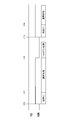
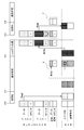
- FIG. 3 is a flowchart for explaining the operation of the electronic control device shown in FIG. 1. It is a timing chart for demonstrating the operation
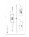
- FIG. 1 shows a schematic configuration of an electronic control unit (ECU) 10 according to an embodiment of the present invention.
- the ECU 10 is for a vehicle that controls an automobile ignition device, a fuel pump, an automatic transmission, and the like.
- the ECU 10 supplies power such as a processor (control unit) 1 such as a CPU (Central Processing Unit), a RAM (Random Access Memory) 2 used as a work area, and an EEPROM (Electrically Erasable and Programmable Read Only Memory) 3. And a non-volatile memory for storing data that can retain data even if the power is shut off.
- the EEPROM 3 is built in the ECU 10 here, it may be mounted externally on the ECU 10.
- the processor 1 acquires information of each part of the vehicle from various sensors, and based on the information from these sensors, the operation amount of the ignition device, fuel pump, automatic transmission, etc. to be controlled, such as ignition timing, fuel injection amount, vehicle speed, A gear ratio according to the rotational speed of the engine is calculated, and control information is output to an ignition device, a fuel pump, an automatic transmission, and the like.
- the processor 1, the RAM 2 and the EEPROM 3 are connected to each other via a bus 4, and data is written and read based on the control of the processor 1.
- the RAM 2 includes a backup area (B / U RAM) to which a data holding voltage is applied from a battery and a normal area for work.
- the RAM 2 can be a normal RAM that is not battery-backed up.
- various control programs corresponding to the control target are stored in advance. When the ignition switch IGN is turned on and the ECU 10 is initialized, these control programs are read from the EEPROM 3 to the normal area of the RAM 2 and used for controlling the control target. Further, during the shutdown process, the learning value generated during the driving cycle (driving cycle DC) and stored in the backup area of the RAM 2 is written and updated in the EEPROM 3, and the failure information by the OBD (On-Board Diagnostics) function is also stored in the EEPROM 3. To remember.
- OBD On-Board Diagnostics
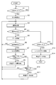
- FIG. 2 shows the operation of the electronic control device shown in FIG.
- the flowchart of FIG. 2 shows an example in which the evacuation data is erased after an instantaneous power interruption and after a shutdown process.
- step S1 it is determined whether or not the ignition switch IGN is on (step S1), and if it is determined to be on, the ECU 10 is initialized (step S2). If it is determined to be off, the determination operation is repeated until it is determined to be on.
- the control program is read from the EEPROM 3 under the control of the processor 1 and written in the normal area of the RAM 2.
- the processor 1 performs normal processing on the controlled object using the control program (step S3).
- the processor 1 calculates operation amounts such as ignition timing, fuel injection amount, and gear ratio based on information from various sensors, and supplies it to the ignition device, fuel pump, automatic transmission, and the like to be controlled.
- Control Data during the running cycle generated during the normal processing operation is stored in the RAM 2.
- step S4 it is determined whether or not a predetermined condition that may cause a power interruption is satisfied. If it is determined that the condition is satisfied, at least a part of the data stored in the RAM 2 under the control of the processor 1 is written in the save area of the EEPROM 3 and the count value is written in the counter area (step S5). Then, it is determined whether or not an instantaneous power interruption has occurred (step S6). If an instantaneous interruption has occurred, the ECU 10 is initialized when the power supply voltage is restored (step S7). Subsequently, it is determined whether or not the data in the save area of the EEPROM 3 is to be written back under the control of the processor 1 (step S8).
- step S9 the data used across the driving cycle can be restored before the instantaneous interruption of the power supply occurs.
- step S10 If it is determined in step S8 that the data in the save area of the EEPROM 3 is not written back, it is determined whether or not the data in the save area is to be erased (step S10). If it is determined to be erased, the data in the save area of the EEPROM 3 is erased and the process returns to the normal operation in step S3 (step S11). If it is determined not to be erased, the data in the save area is not erased and the normal process in step S3 is performed. Return to operation. If it is determined in step S6 that no power interruption has occurred, the process returns to step S3 to perform normal processing.
- step S4 when it is determined in step S4 that the predetermined condition is not satisfied, it is determined whether or not the ignition switch IGN is turned off (step S12).
- the shutdown process is executed. (Step S13), the data in the save area of the EEPROM 3 is erased and the process ends (Step S14).
- the data stored in the RAM 2 under the control of the processor 1 is written in the storage area of the EEPROM 3 and “count value n + 1” is written in the corresponding counter area.
- step S12 If it is determined in step S12 that the ignition switch IGN is on, the process returns to step S3, and the processor 1 executes normal processing on the controlled object using the control program.
- the erasure data erasure in step S11 described above is executed after the ECU 10 is initialized in step S7, that is, after the data is normally read from the backup area of the EEPROM 3 and the RAM 2, so that the data reliability is high.
- the erasure since the erasure is performed after the ignition is turned on until the vehicle operation is started, the erasure may not be completed if the processor 1 stops at a timing such as cranking.
- the erasure data is erased in step S14 before the power supply to the backup area of the RAM 2 and the processor 1 is stopped, so that the erasing operation can be basically performed in a stable power system.
- the backup at the ignition-off time is successful, there is a possibility that data may be lost if the reading fails at the initialization of the ECU 10 at the ignition-on time.
- step S11 and step S14 data erasure can be executed more reliably. This is because if the erasure is not normal before the processor 1 is stopped, the erasure can be executed when the ignition is turned on. However, since the erase determination operation is required twice, the processing becomes redundant and the processing time becomes slightly longer. Accordingly, the evacuation data may be deleted by selecting one or both of step S11 and step S14 as necessary in consideration of the advantages and disadvantages as described above.
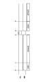
- FIG. 3A and FIG. 3B are diagrams for explaining an operation at the time of power supply interruption in the electronic control device shown in FIG.
- FIG. 3A shows the operation timing of the ECU 10 with respect to the state of the ignition switch IGN and the battery voltage VB.
- FIG. 3B schematically shows a data writing operation and a data reading operation with respect to the RAM 2 and the EEPROM 3 in association with the operation of the ECU 10 in FIG. 3A.
- the ECU 10 is initialized at the timing (time t0) when the ignition switch IGN is turned on (“H” level).
- initialization of the ECU 10 writes data read from the EEPROM 3 to the RAM 2 under the control of the processor 1.
- the storage area of the EEPROM 3 has a bank 0, a bank 1, and a save area.
- Each of the bank 0, the bank 1, and the save area includes a data storage area and a counter area for storing a count value.
- a normal RAM that is not backed up by a battery may be used.
- the data in the storage area corresponding to the count value n (including the control program) is the newest, and the latest data is stored in the bank 0.
- the latest data of bank 0 in the EEPROM 3 is read and written in the backup area of the RAM 2.
- normal processing is subsequently executed.
- the processor 1 performs work using the normal area of the RAM 2.
- Data used across the driving cycle of the vehicle generated during this work (operation) is written in the backup area.
- Data used across the driving cycle includes failure information (diagnostic information for each device, failure warning light MIL on / off, etc.), learning values, display data for diagnostic tools, and storage information when a failure occurs. is there. For example, when any failure (abnormality) is detected, the failure information and the like are written in the backup area of the RAM 2.
- the predetermined condition is a case where the battery voltage VB (power supply voltage) is expected to decrease to a level at which the operation of the processor 1 serving as the control unit is stopped. When a larger current flows, the battery voltage VB is predicted to be decreased, or the battery voltage VB is measured and the decrease is detected.
- the battery voltage VB power supply voltage
- the starter when the starter is activated, immediately before reset by self-diagnosis of the processor 1, when the battery is deteriorated due to aging, etc., when a device with high power consumption such as an air conditioner is activated, or when the device such as a power window or light is activated simultaneously Or a combination of these multiple conditions.
- the battery deterioration can be predicted from the fluctuation of the battery voltage VB depending on the presence or absence of a load and the voltage recovery time.
- the data to be written in the save area of the EEPROM 3 is data generated during the operation of the ECU 10 and used across the driving cycle, for example, data stored until the battery voltage VB decreases after the ignition switch IGN is turned on. . Specifically, it includes the above-described failure information, learning value, display data for the diagnostic tool, storage information at the time of failure occurrence, etc. Here, failure information indicating whether or not the failure warning lamp MIL is turned on, etc. Is used. Further, snapshots at the time of failure occurrence, drive recorder data, and the like may be included. Then, the count value of the bank storing the latest data read from the EEPROM 3 in the current travel cycle is written in the counter area of the save area.
- the starter is activated for starting from starting or stopping the engine or if a large current flows for some reason, the battery voltage VB may be lower than the operating voltage of the processor 1. .
- the ECU 10 is initialized by a power-on reset of the processor 1.
- the processor 1 At the time of this power-on reset, it is determined whether or not the processor 1 ended normally last time, in other words, whether or not it is an illegal reset.
- An unauthorized reset is when the battery voltage VB is temporarily reduced to a level at which the operation of the processor 1 stops when the ignition switch IGN of the vehicle to be controlled is on, and the engine is started (restarts operation). In this operation, the processor 1 is reset. If it is determined that the reset is illegal, the data written in the save area of the EEPROM 3 at the time of initialization is written back to the RAM 2.
- the latest data (count value n) is read from the data storage area of the bank 0 of the EEPROM 3 and written to the backup area of the RAM 2.
- the storage information at the time of failure for example, information indicating whether or not the failure warning lamp MIL is lit
- the data saved in the EEPROM 3 can be recovered by writing it back at the time of power-on reset. Therefore, even if a power interruption occurs and data across the driving cycle (for example, information indicating whether or not the failure warning lamp MIL is lit) disappears from the RAM 2, it is retained in the save area of the EEPROM 3, and the power Because it can be restored by initialization after a momentary interruption, merchantability and failure analysis ability can be improved.
- the ECU 10 When the initialization is completed, the ECU 10 performs normal processing using the backup area and the normal area of the RAM 2 (time t4). The operation described above is repeated after time t4.
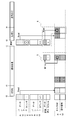
- FIG. 4A and 4B are diagrams for explaining an operation at the time of normal shutdown.
- FIG. 4A shows the operation timing of the ECU 10 with respect to the state of the ignition switch IGN and the battery voltage VB.
- FIG. 4B schematically shows a data writing operation and a data reading operation with respect to the RAM 2 and the EEPROM 3 in association with the operation of the ECU 10 in FIG. 4A.
- the ECU 10 is initialized at the timing (time t10) when the ignition switch IGN is turned on (“H” level). As shown in FIG. 4B, the initialization of the ECU 10 writes the data read from the EEPROM 3 under the control of the processor 1 into the RAM 2.
- the data in the storage area corresponding to the count value n is the newest, and the latest data is stored in the bank 0.
- the latest data in the bank 0 of the EEPROM 3 is read and written in the backup area of the RAM 2.
- the processor 1 performs work using the normal area of the RAM 2. Data used across the driving cycle of the vehicle generated during this work (operation) is written in the backup area.
- a predetermined condition is satisfied during the time t11-t12 during which the normal processing is performed, a part of the data stored in the backup area of the RAM 2 is saved in the save area data in the EEPROM 3, as shown by the alternate long and short dash line 5.
- the count value n is written to the counter area.
- the shutdown process is performed when the ignition switch IGN is turned off.
- the data in the backup area of the RAM 2 is written into the data storage area of the bank 1 in the EEPROM 3. Further, “count value n + 1” is written in the counter area of bank 1.
- the processor 1 ends normally.
- the ECU 10 When the ignition switch IGN is turned on at time t13 after a predetermined time has elapsed, the ECU 10 is initialized by a power-on reset of the processor 1. At power-on reset, the latest data is read from the data storage area of bank 1 of EEPROM 3 and written to the backup area of RAM 2. At this time, since the count value (n) of the saving area is different from the count value (n + 1) of the bank 1 storing the latest data in the EEPROM 3, the backup area of the RAM 2 is not overwritten and is surrounded by a one-dot chain line 7. As shown, the save area (data storage area and counter area) in the EEPROM 3 is erased. Alternatively, after the shutdown process is completed, the save area in the EEPROM 3 is erased.
- the ECU 10 When initialization is completed, the ECU 10 performs normal processing using the backup area and the normal area of the RAM 2 (time t14). The operation described above is repeated after time t14. Therefore, at the time of normal shutdown, the data used across the driving cycle is updated using the backup area of the RAM 2 and is written and held in the save area of the EEPROM 3, and is initialized, Processing and shutdown processing can be executed.
- the data used across the driving cycle is written in the save area of the EEPROM 3, and the data written in the save area when the operation is restarted from the illegal reset is stored in the RAM. Write back and restore.
- the failure warning light can be turned off or the learning value can be updated to the latest state. Can improve the analysis ability.
- a part of the data stored in the backup area of the RAM 2 is written in the data storage area of the save area.
- all data stored in the backup area may be written.
- processor control unit
- RAM random access memory
- EEPROM nonvolatile memory
- bus 10
- ECU electronic control unit
Landscapes
- Engineering & Computer Science (AREA)
- Theoretical Computer Science (AREA)
- Physics & Mathematics (AREA)
- General Engineering & Computer Science (AREA)
- General Physics & Mathematics (AREA)
- Computer Hardware Design (AREA)
- Quality & Reliability (AREA)
- Techniques For Improving Reliability Of Storages (AREA)
- Combined Controls Of Internal Combustion Engines (AREA)
- Retry When Errors Occur (AREA)
- For Increasing The Reliability Of Semiconductor Memories (AREA)
Abstract
電源の瞬断が発生しても、動作中に生じたデータを保持でき、商品性や故障の解析能力を向上できる電子制御装置を提供する。 電子制御装置は、作業領域として用いるRAMと、データ保存用の不揮発性メモリと、RAM及び不揮発性メモリへのデータの書き込み及び読み出しを制御する制御部とを備える。制御部は、動作中に発生したデータをRAMに格納させ、動作を停止するときにデータを不揮発性メモリの記憶領域に書き込ませ、始動するときにデータを不揮発性メモリからRAMに読み出して制御対象を制御するように構成されている。この制御部は、不正なリセットが予測された場合に、制御部が動作中に発生したデータの少なくとも一部を、RAMから不揮発性メモリにおける前記データの記憶領域とは異なる待避領域に書き込み、不正なリセットから動作を再開するときに、記憶領域と待避領域に書き込んだデータをRAMに読み出す。
Description
本発明は、作業領域として用いるRAMとデータ保存用の不揮発性メモリとを備えた電子制御装置及びそのデータ保護方法に関する。
特許文献1には、RAM上で更新される継続保存対象データを、バッテリバックアップされたSRAMに常時記憶させると共に、不揮発性メモリにも記憶させ、動作開始時にSRAM内のデータが異常と判定された場合に、不揮発性メモリからデータを復元する自動車用の電子制御装置が記載されている。この特許文献1では、外部装置から出力要求を受けた際に、電源の瞬断などで最新のデータが失われないように、不揮発性メモリへの継続保存対象データの記憶が終了してから出力を行う。
しかしながら、この種の電子制御装置では、十分なバッテリ容量が確保できていないと、スタータの作動時などに大電流が流れて電源の瞬断が発生する惧れがある。電源が瞬断すると、バッテリバックアップされたRAMであっても記憶データが破壊される可能性がある。また、電源瞬断によりマイクロコンピュータがリセットされると、継続保存対象データを不揮発性メモリへ書き込むシャットダウン処理が実行されず、更新すべき継続保存対象データを消失する可能性もある。このため、動作中に発生したデータを保持できず、例えば故障警告灯の点灯/消灯制御ができなくなったり、学習値を最新の状態に更新できなかったりする、という課題がある。
本発明は上記のような事情に鑑みてなされたもので、その目的とするところは、電源の瞬断が発生しても、動作中に発生したデータを保持でき、商品性や故障の解析能力を向上できる電子制御装置を提供することにある。
また、本発明の別の目的は、電源の瞬断が発生しても、動作中に発生したデータを保護できる、電子制御装置のデータ保護方法を提供することにある。
また、本発明の別の目的は、電源の瞬断が発生しても、動作中に発生したデータを保護できる、電子制御装置のデータ保護方法を提供することにある。
本発明の電子制御装置は、作業領域として用いるRAMと、データ保存用の不揮発性メモリと、前記RAM及び前記不揮発性メモリへのデータの書き込み及び読み出しを制御し、動作中に発生したデータを前記RAMに格納させ、動作を停止するときに前記データを前記不揮発性メモリの記憶領域に書き込ませ、始動するときに前記データを前記不揮発性メモリから前記RAMに読み出して制御対象を制御するように構成された制御部であって、不正なリセットが予測された場合に、動作中に発生したデータの少なくとも一部を、前記RAMから前記不揮発性メモリにおける前記データの記憶領域とは異なる待避領域に書き込み、不正なリセットから動作を再開するときに、前記記憶領域と前記待避領域に書き込んだデータを前記RAMに読み出す制御部とを具備することを特徴とする。
また、本発明の電子制御装置のデータ保護方法は、制御部の動作中に発生したデータをRAMに格納することと、動作を停止するときに前記データを不揮発性メモリに書き込むことと、始動するときに前記不揮発性メモリから前記データを前記RAMに読み出し、制御対象を制御することと、前記制御部の不正なリセットが予測された場合に、前記動作中に発生したデータの少なくとも一部を、前記RAMから前記不揮発性メモリにおける前記データの記憶領域とは異なる待避領域に書き込むことと、不正なリセットから動作を再開するときに、前記記憶領域と前記待避領域に書き込んだデータを前記RAMに読み出すこととを具備することを特徴とする。
また、本発明の電子制御装置のデータ保護方法は、制御部の動作中に発生したデータをRAMに格納することと、動作を停止するときに前記データを不揮発性メモリに書き込むことと、始動するときに前記不揮発性メモリから前記データを前記RAMに読み出し、制御対象を制御することと、前記制御部の不正なリセットが予測された場合に、前記動作中に発生したデータの少なくとも一部を、前記RAMから前記不揮発性メモリにおける前記データの記憶領域とは異なる待避領域に書き込むことと、不正なリセットから動作を再開するときに、前記記憶領域と前記待避領域に書き込んだデータを前記RAMに読み出すこととを具備することを特徴とする。
本発明では、制御部の不正なリセットが予測された場合に、動作中に発生したデータの少なくとも一部を、不揮発性メモリにおけるデータの記憶領域とは異なる待避領域に書き込んで待避し、不正なリセットから動作を再開するときに、データの記憶領域と待避領域に書き込んだデータをRAMに読み出して制御に用いる。これによって、電源の瞬断が発生してデータがRAMから消失しても、動作中に発生したデータを不揮発性メモリの記憶領域と待避領域に保持したデータで再現できる。従って、電源の瞬断が発生しても、制御部の動作中に発生したデータを保護でき、電子制御装置の商品性や故障の解析能力を向上できる。
以下、本発明の実施形態について図面を参照して説明する。
図1は、本発明の実施形態に係る電子制御装置(ECU)10の概略構成を示している。このECU10は、自動車の点火装置、燃料ポンプ、自動変速機などを制御する車両用である。ECU10は、例えばCPU(Central Processing Unit)のようなプロセッサ(制御部)1と、作業領域として用いるRAM(Random Access Memory)2と、EEPROM(Electrically Erasable and Programmable Read Only Memory)3のような電源供給を遮断してもデータを保持できるデータ保存用の不揮発性メモリとを備えている。ここでは、EEPROM3がECU10に内蔵されているが、ECU10に外付けで実装されてもよい。
図1は、本発明の実施形態に係る電子制御装置(ECU)10の概略構成を示している。このECU10は、自動車の点火装置、燃料ポンプ、自動変速機などを制御する車両用である。ECU10は、例えばCPU(Central Processing Unit)のようなプロセッサ(制御部)1と、作業領域として用いるRAM(Random Access Memory)2と、EEPROM(Electrically Erasable and Programmable Read Only Memory)3のような電源供給を遮断してもデータを保持できるデータ保存用の不揮発性メモリとを備えている。ここでは、EEPROM3がECU10に内蔵されているが、ECU10に外付けで実装されてもよい。
プロセッサ1は、各種センサから車両の各部の情報を取得し、これらセンサからの情報に基づき制御対象の点火装置、燃料ポンプ、自動変速機などの操作量、例えば点火時期、燃料噴射量、車速やエンジンの回転速度に応じた変速比などを算出して、点火装置、燃料ポンプ、自動変速機などへ制御情報を出力する。これらプロセッサ1、RAM2及びEEPROM3は、バス4を介して相互に接続され、プロセッサ1の制御に基づいてデータの書き込みと読み出しが行われるようになっている。
RAM2は、バッテリからデータ保持用の電圧が印加されたバックアップ領域(B/U RAM)と作業用の通常領域とを備えている。このRAM2には、バッテリバックアップされない通常のRAMを用いることもできる。EEPROM3には、例えば制御対象に応じた各種の制御プログラムが予め記憶されている。そして、イグニッションスイッチIGNがオンしてECU10を初期化する時に、これらの制御プログラムをEEPROM3からRAM2の通常領域に読み出して制御対象に対する制御のために用いる。また、シャットダウン処理時に、走行サイクル(ドライビングサイクルDC)中に発生してRAM2のバックアップ領域に記憶した学習値をEEPROM3に書き込んで更新するとともに、OBD(On-Board Diagnostics)機能による故障情報などをEEPROM3に記憶する。
図2は、図1に示した電子制御装置の動作を示している。この図2のフローチャートでは、待避データの消去を、電源の瞬断発生後とシャットダウン処理後に実行する例を示している。まず、イグニッションスイッチIGNがオンしているか否か判定し(ステップS1)、オンと判定されるとECU10の初期化を行う(ステップS2)。オフと判定されると、オンと判定されるまで判定動作を繰り返して待機する。初期化では、プロセッサ1の制御によりEEPROM3から制御プログラムを読み出し、RAM2の通常領域に書き込む。
続いて、プロセッサ1により制御プログラムを用いて制御対象に対して通常処理を行う(ステップS3)。通常処理では、例えば各種センサからの情報に基づきプロセッサ1で点火時期、燃料噴射量、変速比などの操作量を算出し、制御対象である点火装置、燃料ポンプ、自動変速機などに供給して制御する。この通常処理の動作中に発生した走行サイクル中のデータは、RAM2に格納する。
次のステップS4では、電源の瞬断が発生する可能性がある所定の条件が成立したか否かを判定する。条件が成立したと判定されると、プロセッサ1の制御によりRAM2に記憶したデータの少なくとも一部を、EEPROM3の待避領域に書き込むと共に、カウンタ領域にカウント値を書き込む(ステップS5)。そして、電源の瞬断が発生したか否か判定し(ステップS6)、瞬断が発生した場合には電源電圧の回復時にECU10の初期化を行う(ステップS7)。続いて、プロセッサ1の制御によりEEPROM3の待避領域のデータを書き戻すか否か判定し(ステップS8)、書き戻すと判定されると待避領域のデータを読み出してRAM2に書き戻してステップS3の通常処理に戻る(ステップS9)。これによって、電源の瞬断が発生する前に、走行サイクルを跨いで使用するデータを復元することができる。
ステップS8でEEPROM3の待避領域のデータを書き戻さないと判定された場合には、待避領域のデータを消去するか否か判定する(ステップS10)。そして、消去すると判定されるとEEPROM3の待避領域のデータを消去してステップS3の通常動作に戻り(ステップS11)、消去しないと判定されると待避領域のデータを消去せずにステップS3の通常動作に戻る。
なお、ステップS6で、電源の瞬断が発生しなかったと判定された場合には、ステップS3に戻って通常処理を実行する。
なお、ステップS6で、電源の瞬断が発生しなかったと判定された場合には、ステップS3に戻って通常処理を実行する。
一方、ステップS4で所定の条件が成立しないと判定された場合には、イグニッションスイッチIGNがオフになったか否か判定し(ステップS12)、オフになったと判定されたときにシャットダウン処理を実行し(ステップS13)、EEPROM3の待避領域のデータを消去して終了する(ステップS14)。シャットダウン処理では、プロセッサ1の制御によりRAM2に記憶したデータを、EEPROM3の記憶領域に書き込むと共に、対応するカウンタ領域に「カウント値n+1」を書き込む。
また、ステップS12でイグニッションスイッチIGNがオンと判定された場合には、ステップS3に戻り、プロセッサ1により制御プログラムを用いて制御対象に対して通常処理を実行する。
上述したステップS11における待避データの消去は、ステップS7でECU10を初期化した後、すなわちEEPROM3及びRAM2のバックアップ領域から正常に読み出しを行った後に実行するので、データの信頼性が高い。しかし、イグニッションオンしてから車両動作開始までの間に消去を行うため、クランキング等のタイミングでプロセッサ1が停止すると、消去が完了しない可能性がある。
一方、ステップS14における待避データの消去は、RAM2のバックアップ領域とプロセッサ1への電源供給の停止前に実行するので、基本的に電源系が安定した状態で消去動作が可能である。しかし、イグニッションオフ時のバックアップが成功しても、イグニッションオン時においてECU10の初期化時に読み出しが失敗するとデータが消失する可能性がある。
これに対し、ステップS11とステップS14の両方で待避データの消去を行うと、データ消去をより確実に実行できる。これは、プロセッサ1の停止前に消去が正常でないときには、イグニッションオン時に消去を実行できるからである。しかしながら、消去判定動作が2回必要となるので、処理が冗長になり処理時間が若干長くなる。
従って、待避データの消去は、上記のような長所と短所を考慮し、必要に応じてステップS11とステップS14のうち一方を選択、または両方を選択するとよい。
従って、待避データの消去は、上記のような長所と短所を考慮し、必要に応じてステップS11とステップS14のうち一方を選択、または両方を選択するとよい。
図3A及び図3Bはそれぞれ、図1に示した電子制御装置における電源瞬断時の動作を説明するための図である。図3Aは、イグニッションスイッチIGNの状態とバッテリ電圧VBに対するECU10の動作タイミングを示している。また、図3Bは、RAM2とEEPROM3に対するデータの書き込み動作と読み出し動作を図3AにおけるECU10の動作と関連づけて模式的に示している。
図3Aに示すように、イグニッションスイッチIGNがオン(“H”レベル)になったタイミング(時刻t0)で、ECU10の初期化が行われる。ECU10の初期化は、図3Bに示すように、プロセッサ1の制御によりEEPROM3から読み出したデータをRAM2に書き込む。ここで、EEPROM3の記憶領域は、バンク0、バンク1及び待避領域を有している。これらバンク0、バンク1及び待避領域にはそれぞれ、データの記憶領域とカウント値を記憶するカウンタ領域とが含まれている。一方、RAM2にはバックアップ領域と通常領域が含まれる例を示しているが、バッテリバックアップされない通常のRAMを用いても構わない。
本例では、カウント値nに対応する記憶領域のデータ(制御プログラムを含む)が最も新しく、バンク0に最新のデータが記憶されている。このEEPROM3におけるバンク0の最新データを読み出してRAM2のバックアップ領域に書き込む。
時刻t1に初期化が終了すると、続いて通常処理を実行する。時刻t1-t2間の通常処理では、プロセッサ1はRAM2の通常領域を用いて作業を行う。この作業(動作)中に発生した車両の走行サイクルを跨いで使用するデータは、バックアップ領域に書き込む。走行サイクルを跨いで使用するデータとは、故障情報(デバイス毎の診断情報や故障警告灯MILのオン/オフなど)、学習値、診断ツールの表示用データ、及び故障発生時の記憶情報などである。例えば何らかの故障(異常)を検出すると、この故障情報などをRAM2のバックアップ領域に書き込む。
そして、通常処理を行っている時刻t1-t2間に所定の条件が成立すると、一点鎖線5で囲んで示すように、RAM2のバックアップ領域に記憶したデータの一部を、EEPROM3における待避領域のデータ領域に書き込むと共にカウンタ領域にカウント値nを書き込む。
ここで、所定の条件とは、制御部であるプロセッサ1の動作が停止するレベルまでバッテリ電圧VB(電源電圧)が低下することが予想される場合であり、プロセッサ1による車両の制御で所定値より大きな電流が流れたときにバッテリ電圧VBの低下を予測して実施する、又はバッテリ電圧VBを測定し、その低下を検出して実施する。
ここで、所定の条件とは、制御部であるプロセッサ1の動作が停止するレベルまでバッテリ電圧VB(電源電圧)が低下することが予想される場合であり、プロセッサ1による車両の制御で所定値より大きな電流が流れたときにバッテリ電圧VBの低下を予測して実施する、又はバッテリ電圧VBを測定し、その低下を検出して実施する。
具体的には、スタータ作動時、プロセッサ1の自己診断によるリセットの直前、経年変化などによるバッテリの劣化時、エアコンなどの消費電力が大きい機器の作動時、パワーウィンドウやライトなどの機器の同時作動時、あるいはこれら複数の条件の組み合わせなどである。バッテリの劣化に関しては、負荷の有無によるバッテリ電圧VBの変動や電圧の回復時間から予測することができる。
また、EEPROM3の待避領域に書き込むデータは、ECU10の動作中に生じた、走行サイクルを跨いで使用するデータ、例えばイグニッションスイッチIGNがオンしてからバッテリ電圧VBが低下するまでに記憶したデータである。具体的には、上述した故障情報、学習値、診断ツールの表示用データ、及び故障発生時の記憶情報などを含んでおり、ここでは故障警告灯MILが点灯したか否かを示す故障情報などを用いる。また、故障発生時のスナップショットやドライブレコーダのデータ等を含めても良い。そして、今回の走行サイクルでEEPROM3から読み出した、最新のデータを記憶したバンクのカウント値を、待避領域のカウンタ領域に書き込む。
上記通常処理中に、エンジンの始動や停止からの起動のためにスタータが作動したり、何らかの原因などで大きな電流が流れたりすると、バッテリ電圧VBがプロセッサ1の動作電圧よりも低下することがある。そして、所定時間経過後の時刻t3にエンジンが起動すると、プロセッサ1のパワーオンリセットによりECU10の初期化が行われる。
このパワーオンリセット時に、プロセッサ1が前回正常に終了したか否か、換言すれば不正なリセットであるか否かを判定する。不正なリセットとは、制御対象となる車両のイグニッションスイッチIGNがオンの状態で、プロセッサ1の動作が停止するレベルまでバッテリ電圧VBが一時的に低下し、エンジンを起動(動作を再開)するときにプロセッサ1のリセットが行われる動作である。そして、不正なリセットと判定されると、初期化時にEEPROM3の待避領域に書き込んだデータをRAM2に書き戻す動作を行う。
すなわち、まずEEPROM3のバンク0のデータの記憶領域から最新のデータ(カウント値n)を読み出し、RAM2のバックアップ領域に書き込む。この後、待避領域のカウント値とEEPROM3のバンク0のカウント値が同じ(n)場合には、一点鎖線6で囲んで示すように、EEPROM3における待避領域に書き込んだ故障情報、学習値、診断ツールの表示用データ、及び故障発生時の記憶情報など(例えば、故障警告灯MILが点灯したか否かを示す情報)を読み出し、RAM2のバックアップ領域に上書きする。
これによって、イグニッションスイッチIGNのオンから電源瞬断までに記憶した情報がバックアップ領域から消失しても、EEPROM3に待避したデータをパワーオンリセット時に書き戻すことで回復できる。従って、電源の瞬断が発生して、走行サイクルを跨ぐデータ(例えば、故障警告灯MILが点灯したか否かを示す情報)がRAM2から消失しても、EEPROM3の待避領域に保持し、電源の瞬断後の初期化で復元できるので、商品性や故障の解析能力を向上できる。
そして、初期化が終了すると、ECU10はRAM2のバックアップ領域と通常領域を用いて通常処理の作業を行う(時刻t4)。時刻t4以降は、上述した動作を繰り返す。
図4A及び図4Bはそれぞれ、通常のシャットダウン時の動作について説明するための図である。図4Aは、イグニッションスイッチIGNの状態とバッテリ電圧VBに対するECU10の動作タイミングを示している。また、図4Bは、RAM2とEEPROM3に対するデータの書き込み動作と読み出し動作を図4AにおけるECU10の動作と関連づけて模式的に示している。
図4Aに示すように、イグニッションスイッチIGNがオン(“H”レベル)になったタイミング(時刻t10)で、ECU10の初期化が行われる。ECU10の初期化は、図4Bに示すように、プロセッサ1の制御によりEEPROM3から読み出したデータをRAM2に書き込む。
本例では、カウント値nに対応する記憶領域のデータ(制御プログラムを含む)が最も新しく、バンク0に最新のデータが記憶されている。このEEPROM3のバンク0の最新データを読み出してRAM2のバックアップ領域に書き込む。
時刻t11に初期化が終了すると、続いて通常処理を実行する。時刻t11-t12間の通常処理では、プロセッサ1はRAM2の通常領域を用いて作業を行う。この作業(動作)中に発生した車両の走行サイクルを跨いで使用するデータは、バックアップ領域に書き込む。
時刻t11に初期化が終了すると、続いて通常処理を実行する。時刻t11-t12間の通常処理では、プロセッサ1はRAM2の通常領域を用いて作業を行う。この作業(動作)中に発生した車両の走行サイクルを跨いで使用するデータは、バックアップ領域に書き込む。
この通常処理を行っている時刻t11-t12間に、所定の条件が成立すると、一点鎖線5で囲んで示すように、RAM2のバックアップ領域に記憶したデータの一部を、EEPROM3における待避領域のデータ領域に書き込むと共にカウンタ領域にカウント値nを書き込む。
次の時刻t12に、イグニッションスイッチIGNがオフするとシャットダウン処理を行う。シャットダウン処理では、RAM2のバックアップ領域のデータを、EEPROM3におけるバンク1のデータの記憶領域に書き込む。また、バンク1のカウンタ領域には「カウント値n+1」を書き込む。この際、バッテリ電圧VBは正常値であるので、プロセッサ1は正常に終了する。
所定時間経過後の時刻t13にイグニッションスイッチIGNがオンすると、プロセッサ1のパワーオンリセットによりECU10の初期化が行われる。パワーオンリセット時には、EEPROM3のバンク1のデータの記憶領域から最新データを読み出し、RAM2のバックアップ領域に書き込む。この際、待避領域のカウント値(n)がEEPROM3の最新のデータを記憶したバンク1のカウント値(n+1)と異なっているので、RAM2のバックアップ領域に上書きはせず、一点鎖線7で囲んで示すように、EEPROM3における待避領域(データの記憶領域とカウンタ領域)を消去する。あるいは、シャットダウン処理終了後に、EEPROM3における待避領域を消去する。このように、待避領域に書き込んだデータとカウント値を消去することで、誤読み出しされるのを抑制できる。
なお、リプログラム時やテスタクリア時などに、RAM2のバックアップ領域のデータを消去する場合には、EEPROM3の待避領域のデータも消去する必要がある。
なお、リプログラム時やテスタクリア時などに、RAM2のバックアップ領域のデータを消去する場合には、EEPROM3の待避領域のデータも消去する必要がある。
初期化が終了すると、ECU10はRAM2のバックアップ領域と通常領域を用いて通常処理の作業を行う(時刻t14)。時刻t14以降は、上述した動作を繰り返す。
従って、通常のシャットダウン時には、走行サイクルを跨いで使用するデータを、RAM2のバックアップ領域を用いて更新しつつ、EEPROM3の待避領域に書き込んで保持し、従来の通常書き込み処理と同様に初期化、通常処理及びシャットダウン処理を実行できる。
従って、通常のシャットダウン時には、走行サイクルを跨いで使用するデータを、RAM2のバックアップ領域を用いて更新しつつ、EEPROM3の待避領域に書き込んで保持し、従来の通常書き込み処理と同様に初期化、通常処理及びシャットダウン処理を実行できる。
以上説明したように、本発明では、走行サイクルを跨いで使用するデータの少なくとも一部を、EEPROM3の待避領域に書き込み、不正なリセットから動作を再開するときに待避領域に書き込んだデータをRAMに書き戻して復元する。これによって、電源瞬断により走行サイクルを跨ぐデータがRAM2から消失しても、EEPROM3の待避領域に保持できる。従って、電源の瞬断などによるプロセッサ1の不正なリセット後に動作を再開する時に、例えば故障警告灯を消灯させたり、学習値を最新の状態に更新したりすることができるので、商品性や故障の解析能力を向上できる。
なお、上述した実施形態では、RAM2のバックアップ領域に記憶したデータの一部を、待避領域のデータの記憶領域に書き込むようにした。しかし、バックアップ領域に記憶した全てのデータを書き込むようにしても良い。
但し、データ量が増大すると書き込みに要する時間が長くなるため、書き込み開始時と完了時とでデータの整合性が取れなくなったり、書き込み中に電源の瞬断が発生してデータが破壊されたりする可能性が生ずる。よって、書き込みの長時間化による上述したようなリスクと、保持したい情報やその重要性、適用する装置などを考慮して待避するデータを決めると良い。
但し、データ量が増大すると書き込みに要する時間が長くなるため、書き込み開始時と完了時とでデータの整合性が取れなくなったり、書き込み中に電源の瞬断が発生してデータが破壊されたりする可能性が生ずる。よって、書き込みの長時間化による上述したようなリスクと、保持したい情報やその重要性、適用する装置などを考慮して待避するデータを決めると良い。
また、EEPROM3に2つのバンクを設け、交互にデータを書き込んで最新のデータを読み出す例について説明したが、3つ以上のバンクを設けて順次データを書き込んで最新のデータを読み出すようにしても良い。
更に、車両用の電子制御装置を例に取って説明したが、他の様々な電子制御装置に適用できるのはもちろんである。
更に、車両用の電子制御装置を例に取って説明したが、他の様々な電子制御装置に適用できるのはもちろんである。
1…プロセッサ(制御部)、2…RAM、3…EEPROM(不揮発性メモリ)、4…バス、10…電子制御装置(ECU)
Claims (18)
- 作業領域として用いるRAM(Random Access Memory)と、
データ保存用の不揮発性メモリと、
前記RAM及び前記不揮発性メモリへのデータの書き込み及び読み出しを制御し、動作中に発生したデータを前記RAMに格納させ、動作を停止するときに前記データを前記不揮発性メモリの記憶領域に書き込ませ、始動するときに前記データを前記不揮発性メモリから前記RAMに読み出して制御対象を制御するように構成された制御部であって、不正なリセットが予測された場合に、動作中に発生したデータの少なくとも一部を、前記RAMから前記不揮発性メモリにおける前記データの記憶領域とは異なる待避領域に書き込み、不正なリセットから動作を再開するときに、前記記憶領域と前記待避領域に書き込んだデータを前記RAMに読み出す制御部と
を具備することを特徴とする電子制御装置。 - 前記不揮発性メモリは、前記制御対象に応じた制御プログラムが予め記憶される、ことを特徴とする請求項1に記載の電子制御装置。
- 前記制御部は、センサから車両の情報を取得し、前記センサからの情報に基づき前記制御対象の操作量を算出して、前記制御対象を制御する、ことを特徴とする請求項1に記載の電子制御装置。
- 前記制御部は、前記車両のイグニッションスイッチがオンしたときに初期化される、ことを特徴とする請求項3に記載の電子制御装置。
- 前記制御部の動作中に発生したデータは、前記車両の走行サイクルを跨いで使用するデータである、ことを特徴とする請求項3に記載の電子制御装置。
- 前記不揮発性メモリの前記待避領域に書き込むデータは、故障情報、学習値、診断ツールの表示用データ、及び故障発生時の記憶情報の少なくともいずれか1つと、前記不揮発性メモリにおける前記記憶領域に書き込んだ最新のデータに対応するカウント値とを含む、ことを特徴とする請求項1に記載の電子制御装置。
- 前記制御部の不正なリセットは、前記制御対象となる車両のイグニッションスイッチがオンの状態で、前記制御部の動作が停止するレベルまで電源電圧が一時的に低下し、動作を再開するときに前記制御部のリセットが行われる動作である、ことを特徴とする請求項1に記載の電子制御装置。
- 前記制御部の不正なリセットの予測は、前記制御部による車両の制御で所定値より大きな電流が流れる場合に、前記制御部の電源電圧の低下を予測して実施する、又は電源電圧の低下を検出して実施する、ことを特徴とする請求項7に記載の電子制御装置。
- 前記制御部の不正なリセットが予測され、前記制御部のリセットが行われなかった場合に、前記不揮発性メモリの前記待避領域に書き込んだデータを消去する、ことを特徴とする請求項1に記載の電子制御装置。
- 制御部の動作中に発生したデータをRAM(Random Access Memory)に格納することと、
動作を停止するときに前記データを不揮発性メモリに書き込むことと、
始動するときに前記不揮発性メモリから前記データを前記RAMに読み出し、制御対象を制御することと、
前記制御部の不正なリセットが予測された場合に、前記動作中に発生したデータの少なくとも一部を、前記RAMから前記不揮発性メモリにおける前記データの記憶領域とは異なる待避領域に書き込むことと、
不正なリセットから動作を再開するときに、前記記憶領域と前記待避領域に書き込んだデータを前記RAMに読み出すことと
を具備することを特徴とする電子制御装置のデータ保護方法。 - 前記不揮発性メモリに、前記制御対象に応じた制御プログラムを予め記憶すること、を更に具備することを特徴とする請求項10に記載の電子制御装置のデータ保護方法。
- センサから車両の各部の情報を前記制御部で取得することと、前記センサからの情報に基づき前記制御部で前記制御対象の操作量を算出して前記制御対象を制御すること、とを更に具備することを特徴とする請求項10に記載の電子制御装置のデータ保護方法。
- 前記車両のイグニッションスイッチがオンしたときに前記制御部を初期化すること、を更に具備する、ことを特徴とする請求項12に記載の電子制御装置のデータ保護方法。
- 前記制御部の動作中に発生したデータは、車両の走行サイクルを跨いで使用するデータである、ことを特徴とする請求項10に記載の電子制御装置のデータ保護方法。
- 前記不揮発性メモリの前記待避領域に書き込むデータは、故障情報、学習値、診断ツールの表示用データ、及び故障発生時の記憶情報の少なくともいずれか1つと、前記不揮発性メモリにおける前記記憶領域に書き込んだ最新のデータに対応するカウント値とを含む、ことを特徴とする請求項10に記載の電子制御装置のデータ保護方法。
- 前記制御部の不正なリセットは、前記制御対象となる車両のイグニッションスイッチがオンの状態で、前記制御部の動作が停止するレベルまで電源電圧が一時的に低下し、動作を再開するときに前記制御部のリセットが行われる動作である、ことを特徴とする請求項10に記載の電子制御装置のデータ保護方法。
- 前記制御部の不正なリセットの予測は、前記制御部による車両の制御で所定値より大きな電流が流れる場合に、前記制御部の電源電圧の低下を予測して実施すること、又は電源電圧の低下を検出して実施すること、を更に具備することを特徴とする請求項16に記載の電子制御装置のデータ保護方法。
- 前記制御部の不正なリセットが予測され、前記制御部のリセットが行われなかった場合に、前記不揮発性メモリの前記待避領域に書き込んだデータを消去すること、を更に具備することを特徴とする請求項10に記載の電子制御装置のデータ保護方法。
Priority Applications (3)
| Application Number | Priority Date | Filing Date | Title |
|---|---|---|---|
| DE112017005483.4T DE112017005483T5 (de) | 2016-10-31 | 2017-10-24 | Elektronische Steuereinheit und Datenschutzverfahren für diese |
| US16/334,339 US11314634B2 (en) | 2016-10-31 | 2017-10-24 | Electronic control unit and data protection method therefor |
| CN201780057933.6A CN110023911B (zh) | 2016-10-31 | 2017-10-24 | 电子控制装置及其数据保护方法 |
Applications Claiming Priority (2)
| Application Number | Priority Date | Filing Date | Title |
|---|---|---|---|
| JP2016-212894 | 2016-10-31 | ||
| JP2016212894A JP6851110B2 (ja) | 2016-10-31 | 2016-10-31 | 電子制御装置 |
Publications (1)
| Publication Number | Publication Date |
|---|---|
| WO2018079537A1 true WO2018079537A1 (ja) | 2018-05-03 |
Family
ID=62023534
Family Applications (1)
| Application Number | Title | Priority Date | Filing Date |
|---|---|---|---|
| PCT/JP2017/038322 Ceased WO2018079537A1 (ja) | 2016-10-31 | 2017-10-24 | 電子制御装置及びそのデータ保護方法 |
Country Status (5)
| Country | Link |
|---|---|
| US (1) | US11314634B2 (ja) |
| JP (1) | JP6851110B2 (ja) |
| CN (1) | CN110023911B (ja) |
| DE (1) | DE112017005483T5 (ja) |
| WO (1) | WO2018079537A1 (ja) |
Families Citing this family (7)
| Publication number | Priority date | Publication date | Assignee | Title |
|---|---|---|---|---|
| KR102943912B1 (ko) | 2019-02-16 | 2026-03-24 | 고쿠리츠다이가쿠호진 도호쿠다이가쿠 | 디바이스, 센서 노드 및 마이크로 콘트롤러에서의 처리 방법 |
| US10877700B1 (en) * | 2019-08-16 | 2020-12-29 | Silicon Motion, Inc. | Flash memory controller and method capable of efficiently reporting debug information to host device |
| CN110789349A (zh) * | 2019-09-25 | 2020-02-14 | 浙江合众新能源汽车有限公司 | 一种车辆行驶中控制器被重启的处理方法及装置 |
| US12518572B2 (en) | 2020-08-24 | 2026-01-06 | Cummins Inc. | Systems and methods for critical data save in electronic control modules |
| CN117173812B (zh) * | 2023-09-08 | 2026-07-14 | 上海纳恩汽车技术股份有限公司 | 数据记录方法、微控制单元、数据记录装置和车辆 |
| CN117435392A (zh) * | 2023-09-28 | 2024-01-23 | 上海卫星工程研究所 | 应用于空间飞行器的重要数据掉电恢复方法及系统 |
| US12625649B2 (en) | 2024-01-09 | 2026-05-12 | Samsung Electronics Co., Ltd. | Volatile memory, system on chip and electronic device comprising the same |
Citations (4)
| Publication number | Priority date | Publication date | Assignee | Title |
|---|---|---|---|---|
| JP2003216281A (ja) * | 2002-01-24 | 2003-07-31 | Canon Inc | 制御装置 |
| JP2004194364A (ja) * | 2002-12-06 | 2004-07-08 | Hitachi Ltd | 電源装置 |
| JP2008105466A (ja) * | 2006-10-23 | 2008-05-08 | Toyota Motor Corp | 車両用電源制御装置 |
| JP2011100416A (ja) * | 2009-11-09 | 2011-05-19 | Denso Corp | 車載電子制御装置およびメモリ制御方法 |
Family Cites Families (12)
| Publication number | Priority date | Publication date | Assignee | Title |
|---|---|---|---|---|
| US4763333A (en) * | 1986-08-08 | 1988-08-09 | Universal Vectors Corporation | Work-saving system for preventing loss in a computer due to power interruption |
| US20030140261A1 (en) | 2002-01-24 | 2003-07-24 | Minoru Takasaki | Control apparatus |
| JP3960212B2 (ja) | 2002-11-25 | 2007-08-15 | 株式会社デンソー | 電子制御装置 |
| WO2009119224A1 (ja) * | 2008-03-25 | 2009-10-01 | アイシン・エィ・ダブリュ株式会社 | 車両上制御装置への制御用データの書込み方法および車両上制御装置 |
| JP5081076B2 (ja) * | 2008-06-23 | 2012-11-21 | 株式会社リコー | メモリ管理装置、画像形成装置及びメモリ管理方法 |
| JP5212391B2 (ja) * | 2010-01-27 | 2013-06-19 | 日産自動車株式会社 | アイドルストップ制御装置 |
| JP2014061793A (ja) * | 2012-09-21 | 2014-04-10 | Hitachi Automotive Systems Ltd | 自動車用電子制御装置 |
| JP5915490B2 (ja) * | 2012-10-05 | 2016-05-11 | 株式会社デンソー | 電子制御装置 |
| JP6135033B2 (ja) * | 2013-03-04 | 2017-05-31 | レシップホールディングス株式会社 | 電源制御装置 |
| JP2015141575A (ja) * | 2014-01-29 | 2015-08-03 | 京セラドキュメントソリューションズ株式会社 | 画像形成装置および制御方法 |
| US10115218B2 (en) * | 2015-08-20 | 2018-10-30 | Mazda Motor Corporation | Vehicular display device |
| US10049004B2 (en) * | 2015-12-09 | 2018-08-14 | Samsung Electronics Co., Ltd. | Electronic system with memory data protection mechanism and method of operation thereof |
-
2016
- 2016-10-31 JP JP2016212894A patent/JP6851110B2/ja active Active
-
2017
- 2017-10-24 US US16/334,339 patent/US11314634B2/en active Active
- 2017-10-24 DE DE112017005483.4T patent/DE112017005483T5/de active Pending
- 2017-10-24 WO PCT/JP2017/038322 patent/WO2018079537A1/ja not_active Ceased
- 2017-10-24 CN CN201780057933.6A patent/CN110023911B/zh active Active
Patent Citations (4)
| Publication number | Priority date | Publication date | Assignee | Title |
|---|---|---|---|---|
| JP2003216281A (ja) * | 2002-01-24 | 2003-07-31 | Canon Inc | 制御装置 |
| JP2004194364A (ja) * | 2002-12-06 | 2004-07-08 | Hitachi Ltd | 電源装置 |
| JP2008105466A (ja) * | 2006-10-23 | 2008-05-08 | Toyota Motor Corp | 車両用電源制御装置 |
| JP2011100416A (ja) * | 2009-11-09 | 2011-05-19 | Denso Corp | 車載電子制御装置およびメモリ制御方法 |
Also Published As
| Publication number | Publication date |
|---|---|
| US11314634B2 (en) | 2022-04-26 |
| JP2018073161A (ja) | 2018-05-10 |
| JP6851110B2 (ja) | 2021-03-31 |
| CN110023911B (zh) | 2023-07-28 |
| DE112017005483T5 (de) | 2019-07-18 |
| US20190278702A1 (en) | 2019-09-12 |
| CN110023911A (zh) | 2019-07-16 |
Similar Documents
| Publication | Publication Date | Title |
|---|---|---|
| JP6851110B2 (ja) | 電子制御装置 | |
| JP4636118B2 (ja) | 電子機器及びプログラム | |
| US7003382B2 (en) | Electronic control unit for a vehicle | |
| JP2014035730A (ja) | 車両用制御装置 | |
| EP2020497B1 (en) | Electronic control unit | |
| JP3969278B2 (ja) | 電子制御装置 | |
| JP5664454B2 (ja) | 車両用電子制御装置 | |
| JP4001088B2 (ja) | 電子制御装置 | |
| JP4281808B2 (ja) | 車両の制御装置およびその制御方法 | |
| JP6323044B2 (ja) | 車両情報記録装置及びプログラム | |
| WO2008099276A1 (en) | Vehicle control device | |
| JP5635941B2 (ja) | 自動車用電子制御装置 | |
| JP2018134964A (ja) | 自動車用電子制御装置 | |
| JP3644058B2 (ja) | 車載エンジンの電子制御装置及びeepromのデータ再書込制御装置 | |
| JP2004151944A (ja) | 不揮発性記憶装置へのデータの書き込み方法、プログラム、および装置、ならびに車載電子制御装置 | |
| JPH09161493A (ja) | 書換え可能な不揮発性メモリの管理方法 | |
| JP5872982B2 (ja) | 車両用制御装置 | |
| JP7029366B2 (ja) | 自動車用電子制御装置 | |
| JP2007062632A (ja) | 電子制御ユニットおよび異常発生時記憶用データの記憶方法 | |
| JP2006286111A (ja) | 半導体メモリの管理装置 | |
| JP6898186B2 (ja) | 自動車用制御装置及び不揮発性メモリの書き込み方法 | |
| EP2045779A1 (en) | Vehicular control apparatus and program storage medium | |
| JP2015176177A (ja) | 自動車用電子制御装置 | |
| JP6921296B2 (ja) | 電子制御装置 | |
| JP2008077135A (ja) | 演算処理装置、及びカウンタ値演算方法 |
Legal Events
| Date | Code | Title | Description |
|---|---|---|---|
| 121 | Ep: the epo has been informed by wipo that ep was designated in this application |
Ref document number: 17865751 Country of ref document: EP Kind code of ref document: A1 |
|
| 122 | Ep: pct application non-entry in european phase |
Ref document number: 17865751 Country of ref document: EP Kind code of ref document: A1 |