WO2018070120A1 - 発光素子及び発光素子の製造方法 - Google Patents
発光素子及び発光素子の製造方法 Download PDFInfo
- Publication number
- WO2018070120A1 WO2018070120A1 PCT/JP2017/030644 JP2017030644W WO2018070120A1 WO 2018070120 A1 WO2018070120 A1 WO 2018070120A1 JP 2017030644 W JP2017030644 W JP 2017030644W WO 2018070120 A1 WO2018070120 A1 WO 2018070120A1
- Authority
- WO
- WIPO (PCT)
- Prior art keywords
- substrate
- layer
- transparent
- light
- emitting element
- Prior art date
- Legal status (The legal status is an assumption and is not a legal conclusion. Google has not performed a legal analysis and makes no representation as to the accuracy of the status listed.)
- Ceased
Links
Images








Classifications
-
- C—CHEMISTRY; METALLURGY
- C03—GLASS; MINERAL OR SLAG WOOL
- C03C—CHEMICAL COMPOSITION OF GLASSES, GLAZES OR VITREOUS ENAMELS; SURFACE TREATMENT OF GLASS; SURFACE TREATMENT OF FIBRES OR FILAMENTS MADE FROM GLASS, MINERALS OR SLAGS; JOINING GLASS TO GLASS OR OTHER MATERIALS
- C03C15/00—Surface treatment of glass, not in the form of fibres or filaments, by etching
-
- H—ELECTRICITY
- H10—SEMICONDUCTOR DEVICES; ELECTRIC SOLID-STATE DEVICES NOT OTHERWISE PROVIDED FOR
- H10H—INORGANIC LIGHT-EMITTING SEMICONDUCTOR DEVICES HAVING POTENTIAL BARRIERS
- H10H20/00—Individual inorganic light-emitting semiconductor devices having potential barriers, e.g. light-emitting diodes [LED]
- H10H20/80—Constructional details
- H10H20/81—Bodies
- H10H20/819—Bodies characterised by their shape, e.g. curved or truncated substrates
- H10H20/82—Roughened surfaces, e.g. at the interface between epitaxial layers
Definitions
- the present invention relates to a light-emitting element in which a transparent substrate is bonded and a manufacturing method thereof.
- a light-emitting element made of AlGaInP is disclosed in the form of a single-sided two-electrode.
- the light-emitting element having such a shape is divided into a use with a narrow light distribution angle and a wide use, but in a use with a wide light distribution angle, it is necessary to provide a rough surface on the light extraction surface.
- Patent Document 1 discloses a technique for bonding a light emitting element on ITO provided on a glass substrate to roughen the glass substrate, but this is difficult to provide a rough surface on the base material sapphire. Is a cause.
- Patent Document 2 discloses a method of providing a rough surface directly on the substrate side in a light emitting device having a shape having two electrodes on one side. This is because a material capable of providing a rough surface on the substrate is selected. Although it is made of an etching material GaP as a material capable of roughening, it is difficult to increase the diameter of the GaP crystal regardless of whether epitaxial growth is selected or a bulk substrate is selected. Is an unsuitable technology.
- Patent Document 3 discloses a technique for joining transparent substrates. In this method, since the material of the base material to be joined is not limited, the diameter can be increased.
- an inexpensive material that can be obtained from a transparent substrate is an oxide, and a substrate material having a processing accuracy enough to pass through a semiconductor process is limited to a sapphire substrate.
- the sapphire substrate is a difficult-to-etch material, and there is a problem that it is difficult to obtain a rough surface by a wet etching technique.
- the present invention has been made in view of the above problems, and provides a light-emitting element having a light distribution angle increased and a light-emitting efficiency increased in a light-emitting element formed by bonding a transparent substrate, and a method for manufacturing the light-emitting element. For the purpose.
- a light emitting device in which a transparent substrate is bonded to the light extraction surface side, provided is a light emitting device characterized in that a transparent film having a refractive index lower than that of the transparent substrate is provided on the light extraction surface side surface of the transparent substrate, and the surface of the transparent film is roughened.
- the surface of the transparent film is roughened, a light emitting element having an increased light distribution angle and an increased luminous efficiency can be obtained regardless of the material of the transparent substrate. Further, the low refractive index material is formed on the light extraction surface side, so that the total reflection angle is generated, and the luminous efficiency can be further increased.
- the transparent substrate is a sapphire substrate and the transparent film is a SiO 2 film.
- a sapphire substrate can be suitably used for the transparent substrate, and a SiO 2 film can be suitably used for the transparent film.
- a method for manufacturing a light emitting device in which a transparent substrate is bonded to the light extraction surface side, A transparent film having a refractive index lower than that of the transparent substrate is laminated on the surface of the transparent substrate on the light extraction surface side, and the surface of the laminated transparent film is roughened by frost processing by chemical treatment.
- a method for manufacturing a light emitting device is provided.
- the transparent substrate is a sapphire substrate and the transparent film is a SiO 2 film.
- the sapphire substrate which is a material that is difficult to be frosted by chemical treatment
- the transparent film is made of SiO 2 film, so that the surface of the transparent film can be easily frosted by chemical treatment. It can be carried out.
- the frost processing is performed by roughening the surface of the transparent film by etching with a liquid in which hydrofluoric acid and a monovalent to tetravalent inorganic acid or organic acid are mixed.
- Such a method can reliably roughen the surface of the transparent film.
- the surface of the transparent film is roughened in the light-emitting element of the present invention, a light-emitting element having an increased light distribution angle and increased light emission efficiency can be obtained regardless of the material of the transparent substrate.
- the low refractive index material is formed on the light extraction surface side, so that the total reflection angle is generated, and the luminous efficiency can be further increased.
- an inexpensive and high processing precision sapphire substrate can be employ
- a light-emitting element of the present invention it is relatively easy to roughen the surface regardless of the material of the transparent substrate, and relatively easily manufacture a light-emitting element having an increased light distribution angle and increased light emission efficiency. Can do. Furthermore, a low refractive index material is formed on the light extraction surface side, whereby a total reflection angle is generated, and a light emitting element with higher luminous efficiency can be manufactured.
- the sapphire substrate is a difficult-to-etch material, and there is a problem that it is difficult to obtain a rough surface by a wet etching technique.
- a transparent film having a refractive index lower than that of the transparent substrate is provided on the surface of the transparent substrate on the light extraction surface side, and the surface of the transparent film is rough.
- a light emitting element with an increased light distribution angle and increased luminous efficiency can be obtained regardless of the material of the transparent substrate, and a low refractive index material is formed on the light extraction surface side. This has led to the idea that a total reflection angle can be generated and the luminous efficiency can be further increased. And the best form for implementing these was scrutinized and the present invention was completed.
- FIG. 1 shows a first embodiment of a light emitting device of the present invention.
- a transparent substrate 110 is bonded to the light extraction surface 115 side.
- a transparent film 180 having a refractive index lower than that of the transparent substrate 110 is provided on the light extraction surface 115 side of the transparent substrate 110, and the surface of the transparent film 180 is roughened.
- a transparent substrate 110 made of, for example, sapphire, on which a transparent film 180 made of, for example, an SiO 2 film is formed can be suitably used.
- the second dielectric film 121 made of, for example, SiO 2 and having a thickness of about 100 nm may be formed on the opposite side of the transparent substrate 110 from the transparent film 180.
- the surface of the transparent film 180 is roughened, and irregularities are formed.
- the transparent film 180 is made of a material having a refractive index lower than that of the transparent substrate 110. As described above, if the transparent film 180 having a low refractive index is provided on the transparent substrate 110 and the irregularities are formed on the surface of the transparent film 180, the surface can be easily roughened regardless of the material of the transparent substrate 110. It is possible to obtain a light-emitting element that is planarized and has an increased light distribution angle and increased light emission efficiency. Further, since the low refractive index material is formed on the light extraction surface 115 side, a total reflection angle is generated, and the light emission efficiency can be further increased.
- a transparent adhesive layer 125 may be formed on the surface of the second dielectric film 121.
- the transparent adhesive layer 125 can be formed of a plurality of layers, for example, a first adhesive layer 125A and a second adhesive layer 125B.
- a first dielectric film 120 made of, for example, SiO 2 and having a thickness of about 100 nm is formed on the transparent adhesive layer 125.
- the surface of the first dielectric film 120 is made of, for example, AlGaAs, GaAsP, GaP, or the like.
- the current propagation layer 107 can be formed with a thickness of 0.5 to 20 ⁇ m.
- the second electrode 151 is formed on a part (second surface) of the surface of the current propagation layer 107, and the buffer layer 106 is formed on a region (first surface) where the second electrode 151 is not formed. It can be.
- the second electrode 151 includes at least one material selected from Au, Ag, Al, Ni, Pd, Ge, Si, and Sn, and has a thickness of 100 nm or more. Is done.
- the second conductivity type is p-type, it includes at least one material selected from Au, Be, Mg, and Zn and has a thickness of 100 nm or more.
- a buffer layer 106 that relieves lattice irregularities may be formed on the surface of the current propagation layer 107.
- the buffer layer 106 is most preferably formed of InGaP or AlInP. Since there is a lattice mismatch between GaAs x P 1-x (x ⁇ 1) and the AlGaInP-based material or AlGaAs-based material, GaAs x P 1-x (x ⁇ 1) has high-density strain and Threading dislocation enters. The threading dislocation density can be adjusted by the composition x.
- a second semiconductor layer 105 made of AlGaInP or AlGaAs and having a thickness of 0.5 to 1.0 ⁇ m may be formed on the surface of the buffer layer 106.
- the active layer 104 having a thickness of 0.1 to 10 ⁇ m may be formed on the surface.
- the active layer 104 has (Al x Ga 1-x ) y In 1-y P (0 ⁇ x ⁇ 1, 0.4 ⁇ y ⁇ 0.6) or Al z Ga 1-z As ( 0 ⁇ z ⁇ 0.45).
- AlGaInP When it is applied to visible light illumination, it is preferable to select AlGaInP, and when it is applied to infrared illumination, it is preferable to select AlGaAs or InGaAs.
- the design of the active layer 104 is not limited to the above materials because the wavelength can be adjusted by using a superlattice or the like other than the wavelength resulting from the material composition.
- the first semiconductor layer 103 made of AlGaInP or AlGaAs and having a thickness of 0.5 to 1.0 ⁇ m may be formed on the surface of the active layer 104.
- the first electrode 150 may be formed on the surface of the first semiconductor layer 103.
- a desired layer such as the buffer layer 116 may be provided between the first semiconductor layer 103 and the first electrode 150 as necessary.
- the first electrode 150 includes at least one material selected from Au, Ag, Al, Ni, Pd, Ge, Si, and Sn and has a thickness of 100 nm or more. Is done.
- the first conductivity type is p-type, it includes at least one material selected from Au, Be, Mg, and Zn and has a thickness of 100 nm or more.
- the second electrode 151 is provided in the current propagation layer 107 is illustrated, but the second electrode 151 may be provided in the second semiconductor layer 105.
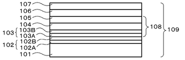
- a substrate 101 is prepared as a starting substrate.
- the substrate 101 it is preferable to use a substrate 101 whose crystal axis is inclined in the [110] direction from the [001] direction.
- the substrate 101 GaAs or Ge can be preferably used. If the substrate 101 is selected from the above materials, the material of the active layer 104 to be described later can be epitaxially grown in a lattice-matched system, so that the quality of the active layer 104 can be easily improved, and the luminance can be increased and the life characteristics can be improved. .
- a first conductive type first semiconductor layer 103 (for example, a thickness of 0.5 to 1.0 ⁇ m) having substantially the same lattice constant as that of the substrate 101 and an active layer 104 (for example, a thickness of 0.1 To 1.0 ⁇ m), second conductivity type second semiconductor layer 105 (for example, thickness of 0.5 to 1.0 ⁇ m), buffer layer 106, and current propagation layer 107 (for example, thickness of about 2.0 ⁇ m) are sequentially grown by epitaxial growth. Can be formed. Further, a selective etching layer 102 for removing the substrate 101 may be inserted between the substrate 101 and the first semiconductor layer 103.
- the selective etching layer 102 has a layer structure of two or more layers, and preferably includes at least a first selective etching layer 102A in contact with the substrate 101 and a second selective etching layer 102B in contact with the first semiconductor layer 103.
- the first selective etching layer 102A and the second selective etching layer 102B may be made of different materials or compositions.
- the MOVPE method metal organic chemical vapor deposition method
- MBE molecular beam epitaxy method
- the buffer layer 106 and the current propagating layer 107 are formed on the light emitting unit 108 including the first conductive type first semiconductor layer 103, the active layer 104, and the second conductive type second semiconductor layer 105 by CBE (Actinic Epitaxy).
- CBE Actinic Epitaxy
- the active layer 104 has (Al x Ga 1-x ) y In 1-y P (0 ⁇ x ⁇ 1, 0.4 ⁇ y ⁇ 0.6) or Al z Ga 1-z As ( 0 ⁇ z ⁇ 0.45).
- AlGaInP When it is applied to visible light illumination, it is preferable to select AlGaInP, and when it is applied to infrared illumination, it is preferable to select AlGaAs or InGaAs.
- the design of the active layer 104 is not limited to the above materials because the wavelength can be adjusted by using a superlattice or the like other than the wavelength resulting from the material composition.
- the material selection is not necessarily the same material system as that of the active layer 104.
- the first semiconductor layer 103, the light emitting layer 104, and the second semiconductor layer 105 having the simplest structure are exemplified by AlInGaP, which is the same material, but the first semiconductor layer 103 or the second semiconductor layer is exemplified.
- the layer 105 generally includes a plurality of layers, and the second semiconductor layer 105 is not limited to a single layer.
- the first semiconductor layer 103 is made of a layer having two or more types of Al composition.
- the second layer 103B is closer to the active layer 104, and the first layer 103A having lower Al composition is closer to the substrate 101. It can be set as the structure which has.
- the second layer 103B is a functional layer having a function of a clad layer, and does not mean a single composition or a single condition layer.
- the current propagation layer 107 AlGaAs, GaAsP, or GaP can be suitably used.
- the buffer layer 106 is most preferably formed of InGaP or AlInP. Since there is a lattice mismatch between GaAs x P 1-x (x ⁇ 1) and the AlGaInP-based material or AlGaAs-based material, GaAs x P 1-x (x ⁇ 1) has high-density strain and Threading dislocation enters. The threading dislocation density can be adjusted by the composition x.
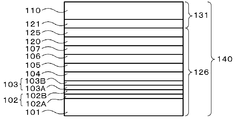
- a first dielectric film (first SiO 2 film) 120 is deposited on the current propagation layer 107 in the epitaxial substrate 109.
- the first dielectric film 120 can be formed by optical CVD, sputtering, or PECVD.
- a transparent adhesive layer 125 can be formed on the first dielectric film 120 to form the first bonding substrate 126.
- the transparent adhesive layer 125 can be selected from BCB (benzocyclobutene) or epoxy. It is preferable to select a material that can be formed by a dipping method or a spin coating method.
- a second dielectric film (second SiO 2 film) 121 can be deposited on the transparent substrate 110 to form the second bonding substrate 131.
- the second dielectric film 121 can be formed by photo CVD, sputtering, or PECVD. It goes without saying that the same effect can be obtained even if a transparent adhesive layer is provided on the second bonding substrate 131.
- the first bonding substrate 126 and the second bonding substrate 131 are placed so that the transparent adhesive layer 125 and the second dielectric film 121 face each other and do not come into contact with each other, and a vacuum atmosphere of 10 Pa or less is set. After the vacuum atmosphere, the transparent adhesive layer 125 and the second dielectric film 121 are brought into contact with each other, and are controlled so as to have a pressure of 5000 N and a temperature between 100 to 200 ° C. and held for 5 minutes or more, and then 100 ° C. or more. Then, the first bonding substrate 126 and the second bonding substrate 131 are pressed to form the bonding substrate 140.
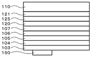
- the substrate 101 is removed from the bonded substrate 140 by etching.
- etching can be performed with a mixed solution of ammonia water and hydrogen peroxide water.
- an etching stop layer (first selective etching layer 102A) made of a material different from that of the substrate 101, etching using a mixed solution of ammonia water and hydrogen peroxide water can be selectively stopped.
- AlInP can be used as the first selective etching layer 102A.
- the first selective etching layer 102A is removed. Since AlInP is used for the etching stop layer 102A, removal is performed using hydrochloric acid. Since the second selective etching layer 102B stops etching with hydrochloric acid, GaAs can be used.
- the first electrode 150 in contact with the first semiconductor layer 103 is formed.
- the first electrode 150 includes at least one material selected from Au, Ag, Al, Ni, Pd, Ge, Si, and Sn and has a thickness of 100 nm or more. can do.
- the first conductivity type is p-type, it can include at least one material selected from Au, Be, Mg, and Zn and have a thickness of 100 nm or more.
- the second selective etching layer 102B may be left.
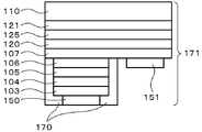
- a pattern in which the first semiconductor layer 103 and the active layer 104 in the region 160 are cut out is formed by etching using a dry method or a wet method.
- FIG. 5 illustrates an example in which the current propagation layer 107 is cut out, the same function is obtained even if the etching is stopped with the second semiconductor layer 105 or the buffer layer 106 exposed.
- a region other than the region 160 is not limited to a flat surface, and a region other than the region 160 may be a rough surface or an uneven surface.
- an insulating layer 170 covering at least part of the first semiconductor layer 103 can be formed. Insulating layer 170, SiO 2, SiNx or the like can be selected.
- a light emitting element substrate 171 in which the second electrode 151 is formed in a part of the region 160 is formed.
- the second conductivity type is n-type, it can include at least one material selected from Au, Ag, Al, Ni, Pd, Ge, Si, and Sn and have a thickness of 100 nm or more.
- the second conductivity type is p-type, it can include at least one material selected from Au, Be, Mg, and Zn and have a film thickness of 100 nm or more.
- a transparent film 180 having a refractive index lower than that of the transparent substrate 110 is laminated on the light extraction surface 115 side of the transparent substrate 110 of the light emitting element substrate 171. Then, the surface of the laminated transparent film 180 is roughened by frost processing by chemical treatment.
- the transparent substrate 110 is preferably a sapphire substrate
- the transparent film 180 is preferably an SiO 2 film.
- the transparent film 180 is made of an SiO 2 film while using a sapphire substrate that is a material that is inexpensive and has high processing accuracy as the transparent substrate 110 but is difficult to be frosted by chemical treatment. Frost processing by chemical treatment can be easily performed on the surface of the steel.
- the SiO 2 film as the transparent film 180 is subjected to frost processing on the surface with a mixed solution of hydrofluoric acid and monovalent to tetravalent inorganic acid or organic acid, and the frost having the uneven layer 181 on the surface of the SiO 2 film.
- the processed substrate 182 can be manufactured. With such a method, it is possible to surely roughen the surface of the transparent film 180 to form irregularities.
- the inorganic acid is composed of at least one of sulfuric acid, hydrochloric acid, and phosphoric acid
- the organic acid is composed of at least one of malonic acid, acetic acid, citric acid, and tartaric acid. it can. If an inorganic acid or an organic acid as described above is used, irregularities can be more reliably formed on the surface of the transparent film.
- the dice are fixed to the stem, and a light emitting diode sealed with an epoxy resin can be manufactured.
- the surface of the transparent film 180 laminated on the transparent substrate 110 is roughened, the surface is easily roughened regardless of the material of the transparent substrate 110, and the light distribution angle is increased and the luminous efficiency is increased.
- a light emitting element can be manufactured relatively easily.
- the low refractive index material is formed on the light extraction surface 115 side, thereby generating a total reflection angle and further improving the light emission efficiency.
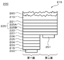
- FIG. 9 shows a second embodiment of the light emitting device of the present invention.
- a transparent substrate 210 is bonded to the light extraction surface 215 side.
- a transparent film 280 having a refractive index lower than that of the transparent substrate 210 is provided on the light extraction surface 215 side of the transparent substrate 210, and the surface of the transparent film 280 is roughened.
- a transparent substrate 210 made of, for example, sapphire, on which a transparent film 280 made of, for example, a SiO 2 film is formed can be suitably used.
- the second dielectric film 221 made of, for example, SiO 2 and having a thickness of about 100 nm may be formed on the opposite side of the transparent substrate 210 from the transparent film 280.
- the surface of the transparent film 280 is roughened, and irregularities are formed.
- the transparent film 280 is made of a material having a refractive index lower than that of the transparent substrate 210. As described above, if the transparent film 280 having a low refractive index is provided on the transparent substrate 210 and the surface of the transparent film 280 is uneven, the surface can be easily roughened regardless of the material of the transparent substrate 210. It is possible to obtain a light-emitting element that is planarized and has an increased light distribution angle and increased light emission efficiency. Further, since the low refractive index material is formed on the light extraction surface 215 side, a total reflection angle is generated, and the light emission efficiency can be further increased.
- irregularities are also formed on the surface of the transparent substrate 210 on the light extraction surface 215 side.
- the transparent substrate 210 is lapped and polished to adjust the thickness.
- polishing since polishing has a long processing time, it is advantageous in cost to perform lapping only.
- the lapping surface is an uneven surface, but the unevenness is small because Ra (roughness) of the unevenness cannot be controlled due to processing restrictions.
- the transparent film 280 By forming the transparent film 280 and forming rough irregularities on the surface, the transparent film 280 has a roughness that can advantageously extract light.
- a transparent adhesive layer 225 may be formed on the surface of the second dielectric film 221.
- the transparent adhesive layer 225 can be formed of a plurality of layers, for example, a first adhesive layer 225A and a second adhesive layer 225B.
- a first dielectric film 220 made of, for example, SiO 2 and having a thickness of about 100 nm is formed on the transparent adhesive layer 225.
- the surface of the first dielectric film 220 is made of, for example, AlGaAs, GaAsP, GaP, or the like.
- the current propagation layer 207 can be formed with a thickness of 0.5 to 20 ⁇ m.
- the second electrode 251 is formed on a part (second surface) of the surface of the current propagation layer 207, and the buffer layer 206 is formed on a region (first surface) where the second electrode 251 is not formed. It can be.
- the second electrode 251 includes at least one material selected from Au, Ag, Al, Ni, Pd, Ge, Si, and Sn, and has a thickness of 100 nm or more. Is done.
- the second conductivity type is p-type, it includes at least one material selected from Au, Be, Mg, and Zn and has a thickness of 100 nm or more.
- a buffer layer 206 that relieves lattice irregularities may be formed on the surface of the current propagation layer 207.
- the buffer layer 206 is most preferably formed of InGaP or AlInP. Since there is a lattice mismatch between GaAs x P 1-x (x ⁇ 1) and the AlGaInP-based material or AlGaAs-based material, GaAs x P 1-x (x ⁇ 1) has high-density strain and Threading dislocation enters. The threading dislocation density can be adjusted by the composition x.
- a second semiconductor layer 205 made of AlGaInP or AlGaAs and having a thickness of 0.5 to 1.0 ⁇ m may be formed on the surface of the buffer layer 206.
- An active layer 204 having a thickness of 0.1 to 10 ⁇ m may be formed on the surface.
- This active layer 204 has (Al x Ga 1-x ) y In 1-y P (0 ⁇ x ⁇ 1, 0.4 ⁇ y ⁇ 0.6) or Al z Ga 1-z As ( 0 ⁇ z ⁇ 0.45).
- AlGaInP When it is applied to visible light illumination, it is preferable to select AlGaInP, and when it is applied to infrared illumination, it is preferable to select AlGaAs or InGaAs.
- the design of the active layer 204 is not limited to the above materials because the wavelength can be adjusted to other than the wavelength resulting from the material composition by using a superlattice or the like.
- the first semiconductor layer 203 made of AlGaInP or AlGaAs and having a thickness of 0.5 to 1.0 ⁇ m may be formed on the surface of the active layer 204.
- the first electrode 250 may be formed on the surface of the first semiconductor layer 203.
- a desired layer such as the buffer layer 216 may be provided between the first semiconductor layer 203 and the first electrode 250 as necessary.
- the first electrode 250 includes at least one material selected from Au, Ag, Al, Ni, Pd, Ge, Si, and Sn, and has a thickness of 100 nm or more. Is done.
- the first conductivity type is p-type, it includes at least one material selected from Au, Be, Mg, and Zn and has a thickness of 100 nm or more.
- the second electrode 251 is provided in the current propagation layer 207 is illustrated, but the second electrode 251 may be provided in the second semiconductor layer 205.
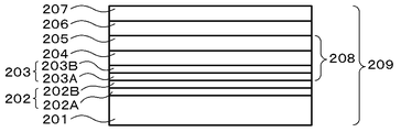
- a substrate 201 is prepared as a starting substrate.
- the substrate 201 it is preferable to use a substrate 201 whose crystal axis is inclined in the [110] direction from the [001] direction.
- the substrate 201 GaAs or Ge can be preferably used. If the substrate 201 is selected from the above materials, the material of the active layer 204 to be described later can be epitaxially grown in a lattice-matched system, so that the quality of the active layer 204 can be easily improved, and the luminance and life characteristics can be improved. .
- a first semiconductor layer 203 (for example, having a thickness of 0.5 to 1.0 ⁇ m) of the first conductivity type having substantially the same lattice constant as that of the substrate 201 and an active layer 204 (for example, having a thickness of 0.1).
- second conductivity type second semiconductor layer 205 (for example, thickness of 0.5 to 1.0 ⁇ m), buffer layer 206, and current propagation layer 207 (for example, thickness of about 2.0 ⁇ m) are sequentially grown by epitaxial growth.
- a selective etching layer 202 for removing the substrate 201 may be inserted between the substrate 201 and the first semiconductor layer 203.
- the selective etching layer 202 has a layer structure of two or more layers, and preferably includes at least a first selective etching layer 202A in contact with the substrate 201 and a second selective etching layer 202B in contact with the first semiconductor layer 203.
- the first selective etching layer 202A and the second selective etching layer 202B may be made of different materials or compositions.
- the substrate 201 on the selective etching layer 202 when the selective etching layer 202 is provided, for example, MOVPE (metal organic chemical vapor deposition) or MBE (molecular beam epitaxy).
- MOVPE metal organic chemical vapor deposition
- MBE molecular beam epitaxy
- the buffer layer 206 and the current propagation layer 207 are formed on the light emitting portion 208 including the first conductive type first semiconductor layer 203, the active layer 204, and the second conductive type second semiconductor layer 205 by CBE (chemical beam epitaxy).
- CBE chemical beam epitaxy
- the epitaxial substrate 209 epitaxially grown in this order can be manufactured.
- the active layer 204 has (Al x Ga 1-x ) y In 1-y P (0 ⁇ x ⁇ 1, 0.4 ⁇ y ⁇ 0.6) or Al z Ga 1-z As ( 0 ⁇ z ⁇ 0.45).
- AlGaInP When it is applied to visible light illumination, it is preferable to select AlGaInP, and when it is applied to infrared illumination, it is preferable to select AlGaAs or InGaAs.
- the design of the active layer 204 is not limited to the above materials because the wavelength can be adjusted to other than the wavelength resulting from the material composition by using a superlattice or the like.
- the material selection is not necessarily the same material system as that of the active layer 204.
- the first semiconductor layer 203, the light emitting layer 204, and the second semiconductor layer 205 having the simplest structure are exemplified by the same material, but the first semiconductor layer 203 or the second semiconductor layer is exemplified.
- 205 generally includes a plurality of layers in order to improve characteristics, and the second semiconductor layer 205 is not limited to a single layer.
- the first semiconductor layer 203 is composed of a layer having two or more types of Al composition.
- the second layer 203B is closer to the active layer 204, and the first layer 203A having lower Al composition is closer to the substrate 201. It can be set as the structure which has.
- the second layer 203B is a functional layer having the function of a cladding layer, and does not mean a single composition or a single condition layer.
- the current propagation layer 207 AlGaAs, GaAsP, or GaP can be suitably used.
- the buffer layer 206 is most preferably formed of InGaP or AlInP. Since there is a lattice mismatch between GaAs x P 1-x (x ⁇ 1) and the AlGaInP-based material or AlGaAs-based material, GaAs x P 1-x (x ⁇ 1) has high-density strain and Threading dislocation enters. The threading dislocation density can be adjusted by the composition x.
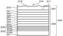
- a first dielectric film (first SiO 2 film) 220 is deposited on the current propagation layer 207 in the epitaxial substrate 209.
- the first dielectric film 220 can be formed by optical CVD, sputtering, or PECVD.
- a transparent adhesive layer 225 can be formed on the first dielectric film 220 to form the first bonding substrate 226.
- BCB benzocyclobutene
- epoxy can be selected. It is preferable to select a material that can be formed by a dipping method or a spin coating method.
- a second dielectric film (second SiO 2 film) 221 can be deposited on the transparent substrate 210 to form the second bonding substrate 231.
- the second dielectric film 221 can be formed by optical CVD, sputtering, or PECVD. It goes without saying that the same effect can be obtained even if a transparent adhesive layer is provided on the second bonding substrate 231.
- the first bonding substrate 226 and the second bonding substrate 231 are placed so that the transparent adhesive layer 225 and the second dielectric film 221 face each other and are not in contact with each other, and a vacuum atmosphere of 10 Pa or less is set. After the vacuum atmosphere, the transparent adhesive layer 225 and the second dielectric film 221 are brought into contact with each other, controlled to be a pressure of 5000 N and a temperature between 100 to 200 ° C. and held for 5 minutes or more, and then 100 ° C. or more. Then, the first bonding substrate 226 and the second bonding substrate 231 are pressure-bonded to form the bonding substrate 240.
- the uneven surface 212 is formed on the light extraction surface 215 side of 210.
- the uneven surface 212 can be mirror-finished by processing such as polishing, it requires processing for a long time, so it is preferable not to perform it here in order to prevent damage to the epitaxial substrate 209. Moreover, it can be advantageous in cost by performing only lapping.
- the substrate 201 is removed from the bonding substrate 240 by etching.
- etching can be performed with a mixed solution of ammonia water and hydrogen peroxide water.
- first selective etching layer 202A By using a material different from that of the substrate 201 for the etching stop layer (first selective etching layer 202A), etching using a mixed solution of ammonia water and hydrogen peroxide water can be selectively stopped.
- AlInP can be used as the first selective etching layer 202A.
- the first selective etching layer 202A is removed. Since AlInP is used for the etching stop layer 202A, removal is performed using hydrochloric acid. Since the second selective etching layer 202B stops etching with hydrochloric acid, GaAs can be used.
- the first electrode 250 in contact with the first semiconductor layer 203 is formed.
- the first electrode 250 includes at least one material selected from Au, Ag, Al, Ni, Pd, Ge, Si, and Sn, and has a thickness of 100 nm or more. can do.
- the first conductivity type is p-type, it can include at least one material selected from Au, Be, Mg, and Zn and have a thickness of 100 nm or more.
- the second selective etching layer 202B may be left behind.
- a pattern in which the first semiconductor layer 203 and the active layer 204 in the region 260 are cut out is formed by etching using a dry method or a wet method.
- FIG. 13 shows an example in which the current propagation layer 207 is cut out, the same function is obtained even if the etching is stopped with the second semiconductor layer 205 or the buffer layer 206 exposed.
- a region other than the region 260 is not limited to a flat surface, and a region other than the region 260 may be a rough surface or an uneven surface.
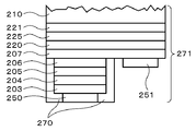
- Insulating layer 270 that covers at least a part of the first semiconductor layer 203 can be formed.
- Insulating layer 270 is, SiO 2, SiNx or the like can be selected.
- a light emitting element substrate 271 in which the second electrode 251 is formed in a part of the region 260 is formed.
- the second conductivity type is n-type, it can include at least one material selected from Au, Ag, Al, Ni, Pd, Ge, Si, and Sn and have a thickness of 100 nm or more.
- the second conductivity type is p-type, it can include at least one material selected from Au, Be, Mg, and Zn and have a film thickness of 100 nm or more.
- a transparent film 280 having a refractive index lower than that of the transparent substrate 210 is laminated on the light extraction surface 215 side surface of the transparent substrate 210 of the light emitting element substrate 271. Then, the surface of the laminated transparent film 280 is roughened by frost processing by chemical treatment.
- the transparent substrate 210 is preferably a sapphire substrate and the transparent film 280 is preferably an SiO 2 film.
- the transparent film 280 is preferably an SiO 2 film.
- the frost processing is performed on the surface of the SiO 2 film, which is the transparent film 280, with a mixed solution of hydrofluoric acid and monovalent to tetravalent inorganic acid or organic acid, and the frosted layer 281 is provided on the surface of the SiO 2 film.
- a processed substrate 282 can be manufactured. With such a method, the surface of the transparent film 280 can be reliably roughened to form irregularities.
- the inorganic acid is composed of at least one of sulfuric acid, hydrochloric acid, and phosphoric acid
- the organic acid is composed of at least one of malonic acid, acetic acid, citric acid, and tartaric acid. it can. If an inorganic acid or an organic acid as described above is used, irregularities can be more reliably formed on the surface of the transparent film.
- the dice are fixed to the stem, and a light emitting diode sealed with an epoxy resin can be manufactured.
- the surface of the transparent film 280 laminated on the transparent substrate 210 is roughened, the surface is easily roughened regardless of the material of the transparent substrate 210, and the light distribution angle is increased and the luminous efficiency is increased.
- a light emitting element can be manufactured relatively easily.
- the low refractive index material is formed on the light extraction surface 215 side, so that the total reflection angle is generated and the luminous efficiency can be further increased.
- the unevenness is also formed on the surface of the transparent substrate 210, light extraction can be performed by laminating a transparent film on the transparent substrate 210 to form rough unevenness on the surface. It has the roughness which can be made more advantageous.
- the refractive index of the transparent substrate on the light extraction surface side is higher than that of the transparent substrate.
- the transparent film having a low thickness is laminated and the surface of the transparent film is roughened.
- the present invention is not limited to this.
- a transparent film may be laminated in advance on the transparent substrate before bonding, and the first bonding substrate may be bonded to the surface of the laminated transparent film subjected to the roughening treatment.
- Example 1 As shown in FIG. 2, a GaAs substrate (substrate 101) having a crystal axis inclined in the [110] direction from the [001] direction was prepared as a starting substrate. Next, an n-type cladding layer (first semiconductor layer 103) having a thickness of 1.0 ⁇ m made of AlGaInP, an active layer 104, and a thickness of 1.0 ⁇ m are formed on the GaAs substrate 101 by MOVPE (metal organic chemical vapor deposition). The p-type cladding layer (second semiconductor layer 105) was epitaxially grown, and a buffer layer 106 made of InGaP and a current propagation layer 107 made of GaP having a thickness of 2.0 ⁇ m were sequentially formed by epitaxial growth. A selective etching layer 102 (also called an etching stop layer) composed of an AlInP layer and a GaAs layer was formed between the GaAs substrate and the n-type cladding layer.
- MOVPE metal organic chemical vapor deposition
- the first semiconductor layer 103 is composed of two or more types of Al compositions, and the first layer 103A having a low Al composition is formed on the side close to the substrate 101.
- a first SiO 2 film (first dielectric film 120) was formed on the current propagation layer 107 made of GaP by PECVD using TEOS and O 2 as raw materials.
- a transparent adhesive layer 125 was formed on the first dielectric film 120, and a first bonding substrate 126 was formed.
- cycloten was dropped and spin coating was performed at a rotational speed of 1,000 rpm. After spin coating, the solvent was volatilized by maintaining on a hot plate at a temperature of 100 ° C. for 60 seconds.
- a sapphire substrate was prepared as the transparent substrate 110, and a second SiO 2 film (second dielectric film 121) was deposited on the transparent substrate 110 to form a second bonded substrate 131.
- the second dielectric film 121 was formed by PECVD using TEOS and O 2 as raw materials.
- the first bonding substrate 126 and the second bonding substrate 131 were placed so that the transparent adhesive layer 125 and the second dielectric film 121 face each other and were not in contact with each other, and a vacuum atmosphere of 10 Pa or less was set. After the vacuum atmosphere, the transparent adhesive layer 125 and the second dielectric film 121 are brought into contact with each other and controlled to a pressure of 5000 N and a temperature of 100 ° C. for 10 minutes, and then heat of 100 ° C. or higher is applied. The first bonded substrate 126 and the second bonded substrate 131 were pressure bonded to form the bonded substrate 140. Thereafter, in order to obtain a desired thickness, lapping and polishing were performed on the surface of the sapphire substrate.
- the substrate 101 was removed from the bonding substrate 140 by etching with a mixed solution of ammonia water and hydrogen peroxide solution. After removing the substrate 101, the first selective etching layer 102A was removed. Since the first selective etching layer 102A used AlInP, hydrochloric acid was used for removal. Next, a first electrode 150 having a thickness of 500 nm made of an AuGeNi alloy in contact with the first semiconductor layer 103 was formed.
- a pattern in which the first semiconductor layer 103, the active layer 104, the second semiconductor layer 105, and the buffer layer 106 in the region 160 were cut out was formed by etching using a dry method.
- an insulating layer 170 covering the first semiconductor layer 103, the active layer 104, the second semiconductor layer 105, and the buffer layer 106 was formed.
- the insulating layer 170 was formed by PECVD using TEOS and O 2 as raw materials.
- the film thickness was 100 nm.
- a second electrode 151 made of an AuBe alloy and having a thickness of 500 nm was formed in part of the region 160, and a light emitting element substrate 171 was formed.
- a SiO 2 film was formed as a transparent film 180 on the light extraction surface 115 side surface of the transparent substrate 110 of the light emitting element substrate 171.
- the transparent film 180 was subjected to a frost treatment on the surface with a mixed solution of hydrofluoric acid and acetic acid, so that a frosted substrate 182 having an uneven layer 181 on the surface of the transparent film 180 was produced.
- the dice were fixed to the stem, and a light emitting diode sealed with an epoxy resin was manufactured.
- Example 2 After joining the sapphire substrate, thin film processing is performed on the sapphire substrate to a specified thickness by lapping, and subsequent polishing is not performed. Manufactured.
- Example 2 A light emitting diode was manufactured in the same manner as in Example 1 except that the SiO 2 film was not formed on the surface of the sapphire substrate.
- FIG. 17 shows the difference in light distribution characteristics of the light emitting diodes manufactured in Example 1, Example 2, and Comparative Example.
- the comparative example has a light distribution angle of around ⁇ 30 degrees, while the first and second embodiments have a relative light distribution angle of 50% or more with respect to the light distribution angle of ⁇ 60 degrees. It has light distribution intensity, and it can be seen that the light distribution angle is widened.
- FIG. 18 shows current-luminance characteristics of the light-emitting diodes manufactured in Example 1, Example 2, and Comparative Example. It can be seen that Example 1 and Example 2 maintain the linearity of the current-luminance characteristics, although the luminance is generally high compared to the comparative example.
- the present invention is not limited to the above embodiment.
- the above-described embodiment is an exemplification, and the present invention has any configuration that has substantially the same configuration as the technical idea described in the claims of the present invention and that exhibits the same effects. Are included in the technical scope.
Landscapes
- Chemical & Material Sciences (AREA)
- Life Sciences & Earth Sciences (AREA)
- Engineering & Computer Science (AREA)
- Chemical Kinetics & Catalysis (AREA)
- General Chemical & Material Sciences (AREA)
- Geochemistry & Mineralogy (AREA)
- Materials Engineering (AREA)
- Organic Chemistry (AREA)
- Led Devices (AREA)
- Surface Treatment Of Glass (AREA)
Abstract
本発明は、光取り出し面側に透明基板が貼り合わせられた発光素子において、前記透明基板の前記光取り出し面側の表面に、前記透明基板より屈折率の低い透明膜が設けられ、該透明膜の表面が粗面化されたものであることを特徴とする発光素子である。これにより、透明基板を接合して形成した発光素子において、配光角度の増大と発光効率の増大した発光素子及び発光素子の製造方法が提供される。
Description
本発明は、透明基板を貼り合わせた発光素子及びその製造方法に関する。
AlGaInPからなる発光素子において片面2電極の形状のものが開示されている。このような形状の発光素子において、配光角度が狭い用途と広い用途に分かれるが、配光角が広い用途の場合、光取り出し面に粗面を設けることが必要である。
特許文献1にはガラス基板上に設けたITO上に発光素子を接合し、ガラス基板を粗面化する技術が開示されているが、これは基材のサファイアに粗面を設けることが難しいことが一因である。
一方、特許文献2では片面2電極を有する形状の発光素子において、基材側に直接粗面を設ける方法が開示されている。これは基材に粗面を設けることが可能な材料を選択しているためである。粗面化可能な材料としてエッチング可能な材料GaPで形成しているが、GaP結晶はエピタキシャル成長を選択するにせよ、バルク基板を選択するにせよ大口径化が難しく、大型の発光素子を作製するには向かない技術である。
一方、特許文献3では透明基板を接合する技術が開示されている。この手法では、接合する基材の材質は問わないため、大口径化が可能である。
しかし、透明基板の材料で安価に手に入る材料は酸化物であり、半導体工程に通せる程度の加工精度を有する基板材料としてはサファイア基板に限定される。しかしながら、サファイア基板は難エッチング材料であり、ウェットエッチングの手法で粗面を得ることが難しいという問題があった。
本発明は上記のような問題に鑑みてなされたもので、透明基板を接合して形成した発光素子において、配光角度の増大と発光効率の増大した発光素子及び発光素子の製造方法を提供することを目的とする。
上記目的を達成するために、本発明によれば、光取り出し面側に透明基板が貼り合わせられた発光素子において、
前記透明基板の前記光取り出し面側の表面に、前記透明基板より屈折率の低い透明膜が設けられ、該透明膜の表面が粗面化されたものであることを特徴とする発光素子を提供する。
前記透明基板の前記光取り出し面側の表面に、前記透明基板より屈折率の低い透明膜が設けられ、該透明膜の表面が粗面化されたものであることを特徴とする発光素子を提供する。
このように、透明膜の表面が粗面化されたものであるので、透明基板の材質に関わらず、配光角度の増大と発光効率の増大した発光素子とすることができる。更に低屈折率材料が光取り出し面側に形成されることで全反射角を生じ、発光効率をより高くすることができる。
このとき、前記透明基板がサファイア基板であり、前記透明膜がSiO2膜であることが好ましい。
このように、透明基板にサファイア基板、透明膜にSiO2膜を好適に用いることができる。
また本発明によれば、光取り出し面側に透明基板を貼り合わせた発光素子の製造方法であって、
前記透明基板の前記光取り出し面側の表面に、前記透明基板より屈折率の低い透明膜を積層し、積層した前記透明膜の表面を化学処理によるフロスト加工により粗面化処理することを特徴とする発光素子の製造方法を提供する。
前記透明基板の前記光取り出し面側の表面に、前記透明基板より屈折率の低い透明膜を積層し、積層した前記透明膜の表面を化学処理によるフロスト加工により粗面化処理することを特徴とする発光素子の製造方法を提供する。
このようにすれば、透明基板の材質に関係なく容易に表面を粗面化し、配光角度の増大と発光効率の増大した発光素子を比較的容易に製造することができる。更に低屈折率材料が光取り出し面側に形成されることで全反射角を生じ、発光効率がより高い発光素子を製造することができる。
このとき、前記透明基板をサファイア基板とし、前記透明膜をSiO2膜とすることが好ましい。
このようにすれば、透明基板として化学処理によるフロスト加工が困難な材料であるサファイア基板を用いつつ、透明膜をSiO2膜とすることにより、透明膜の表面に化学処理によるフロスト加工を容易に行うことができる。
またこのとき、前記フロスト加工は、弗酸と1価~4価の無機酸あるいは有機酸とを混合した液によりエッチング処理することで、前記透明膜の表面を粗面化処理することが好ましい。
このような方法であれば、確実に透明膜の表面を粗面化処理することができる。
またこのとき、前記無機酸として、硫酸・塩酸・燐酸のうちの少なくともいずれか1種を用い、前記有機酸として、マロン酸・酢酸・クエン酸・酒石酸のうちの少なくともいずれか1種を用いることが好ましい。
無機酸あるいは有機酸として、上記のようなものを用いれば、より確実に透明膜の表面に凹凸を形成することができる。
本発明の発光素子であれば、透明膜の表面が粗面化されたものであるので、透明基板の材質に関わらず、配光角度の増大と発光効率の増大した発光素子とすることができる。更に低屈折率材料が光取り出し面側に形成されることで全反射角を生じ、発光効率をより高くすることができる。そして、本発明であれば、透明基板として安価で加工精度の高いサファイア基板を採用することができる。
また、本発明の発光素子の製造方法であれば、透明基板の材質に関係なく容易に表面を粗面化し、配光角度の増大と発光効率の増大した発光素子を比較的容易に製造することができる。更に低屈折率材料が光取り出し面側に形成されることで全反射角を生じ、発光効率がより高い発光素子を製造することができる。
以下、本発明について実施の形態を説明するが、本発明はこれに限定されるものではない。
上記したように、サファイア基板は難エッチング材料であり、ウェットエッチングの手法で粗面を得ることが難しいという問題があった。
そこで、本発明者はこのような問題を解決すべく鋭意検討を重ねた。その結果、光取り出し面側に透明基板が貼り合わせられた発光素子において、透明基板の光取り出し面側の表面に、透明基板より屈折率の低い透明膜が設けられ、該透明膜の表面が粗面化されたものであれば、透明基板の材質に関わらず、配光角度の増大と発光効率の増大した発光素子とすることができ、更に低屈折率材料が光取り出し面側に形成されることで全反射角を生じ、発光効率をより高くすることができることに想到した。そして、これらを実施するための最良の形態について精査し、本発明を完成させた。
(第一の実施形態)
図1に本発明の発光素子の第一の実施形態を示した。図1に示すように、本発明の第一の実施形態における発光素子100は、光取り出し面115側に透明基板110が貼り合わせられている。また、発光素子100は、透明基板110の光取り出し面115側の表面に、透明基板110より屈折率の低い透明膜180が設けられ、該透明膜180の表面が粗面化されたものである。粗面の粗さはRa(算術平均粗さ)=0.3μm以上とすることが好ましい。
図1に本発明の発光素子の第一の実施形態を示した。図1に示すように、本発明の第一の実施形態における発光素子100は、光取り出し面115側に透明基板110が貼り合わせられている。また、発光素子100は、透明基板110の光取り出し面115側の表面に、透明基板110より屈折率の低い透明膜180が設けられ、該透明膜180の表面が粗面化されたものである。粗面の粗さはRa(算術平均粗さ)=0.3μm以上とすることが好ましい。
このとき、表面に例えばSiO2膜等からなる透明膜180が形成された例えばサファイア等からなる透明基板110を好適に用いることができる。また、透明基板110の透明膜180と反対側に例えばSiO2からなる厚さ100nm程度の第二誘電体膜121が形成されたものとすることができる。
上記のように、透明膜180の表面は粗面化されており、凹凸が形成されている。また、透明膜180は透明基板110より低い屈折率の材料が用いられる。このように、透明基板110に対し屈折率の低い透明膜180が設けられ、該透明膜180の表面に凹凸が形成されるようにすれば、透明基板110の材質に関係なく容易に表面を粗面化し、配光角度の増大と発光効率の増大した発光素子とすることができる。また、低屈折率材料が光取り出し面115側に形成されることで全反射角を生じ、発光効率をより高くすることができる。
また、第二誘電体膜121表面には透明接着層125が形成されたものとすることができる。この透明接着層125は、例えば第一接着層125A及び第二接着層125Bの複数の層から形成されたものとすることができる。更に、この透明接着層125には例えばSiO2からなる厚さ100nm程度の第一誘電体膜120が形成されており、第一誘電体膜120の表面には、例えばAlGaAs、GaAsP、GaP等からなる電流伝播層107が0.5~20μmの厚さで形成されたものとすることができる。
また、電流伝播層107の表面の一部(第二面)に第二電極151が形成され、第二電極151が形成されていない領域(第一面)には緩衝層106が形成されたものとすることができる。
第二電極151は、第二導電型がn型の場合、Au,Ag,Al,Ni,Pd,Ge,Si,Snから少なくとも一種類以上の材料を含み、100nm以上の膜厚を有するものとされる。第二導電型がp型の場合、Au、Be,Mg,Znから少なくとも一種類以上の材料を含み、100nm以上の膜厚を有するものとされる。
電流伝播層107の表面には格子不整を緩和する緩衝層106が形成されたものとすることができる。このとき、電流伝播層107をGaAsxP1-x(0≦x<1)で形成した場合、緩衝層106は、InGaPあるいはAlInPで形成するのが最も好適である。GaAsxP1-x(x≠1)と、AlGaInP系材料またはAlGaAs系材料との間には格子不整が存在するため、GaAsxP1-x(x≠1)には高密度のひずみや貫通転位が入る。貫通転位密度は組成xにより調整可能である。
緩衝層106の表面には、AlGaInPもしくはAlGaAsからなる厚さ0.5~1.0μmの第二半導体層105が形成されたものとすることができる。その表面には厚さ0.1~10μmの活性層104が形成されたものとすることができる。この活性層104は発光波長に応じて(AlxGa1-x)yIn1-yP(0≦x≦1,0.4≦y≦0.6)またはAlzGa1-zAs(0≦z≦0.45)で形成されたものとすることができる。可視光照明に適用する場合、AlGaInPを選択するのが好適であり、赤外照明に適用する場合、AlGaAsあるいはInGaAsを選択するのが好適である。ただし、活性層104の設計に関しては、超格子等の利用により波長は材料組成に起因する波長以外に調整可能であるため、上記の材料に限られない。
活性層104の表面にはAlGaInPもしくはAlGaAsからなる厚さ0.5~1.0μmの第一半導体層103が形成されたものとすることができる。第一半導体層103の表面には第一電極150が形成されたものとすることができる。このとき、第一半導体層103と第一電極150との間に必要に応じてバッファ層116等の所望の層を設けてもよい。
第一電極150は、第一導電型がn型の場合、Au,Ag,Al,Ni,Pd,Ge,Si,Snから少なくとも一種類以上の材料を含み、100nm以上の膜厚を有するものとされる。第一導電型がp型の場合、Au、Be,Mg,Znから少なくとも一種類以上の材料を含み、100nm以上の膜厚を有するものとされる。
本実施形態では、電流伝播層107に第二電極151を設ける場合を例示したが、第二半導体層105に第二電極151を設けても良い。
次に、本発明の第一の実施形態における発光素子の製造方法について、図2~図8を用いて説明する。
最初に、図2に示すように、出発基板として、基板101を準備する。基板101として、結晶軸が[001]方向より[110]方向に傾斜した基板101を用いることが好ましい。また、基板101としては、GaAsまたはGeを好適に用いることができる。基板101を上記材料から選択すれば、後述する活性層104の材料を格子整合系でエピタキシャル成長を行うことができるため、活性層104の品質を向上させやすく、輝度上昇や寿命特性の向上が得られる。
次に、基板101上に、基板101と格子定数が略同一の第一導電型の第一半導体層103(例えば厚さ0.5~1.0μm)、活性層104(例えば厚さ0.1~1.0μm)、第二導電型の第二半導体層105(例えば厚さ0.5~1.0μm)、緩衝層106、電流伝播層107(例えば厚さ2.0μm程度)をエピタキシャル成長により順次形成することができる。また、基板101と第一半導体層103の間には、基板101の除去用の選択エッチング層102が挿入されてもよい。選択エッチング層102は二層以上の層構造からなり、基板101に接する第一の選択エッチング層102A、第一半導体層103に接する第二の選択エッチング層102Bを少なくとも有することが好ましい。第一の選択エッチング層102Aと第二の選択エッチング層102Bは異なる材料あるいは組成から構成しても良い。
このとき、具体的には、基板101上(選択エッチング層102を設けた場合には、選択エッチング層102上)に、例えばMOVPE法(有機金属気相成長法)やMBE(分子線エピタキシー法)、CBE(化学線エピタキシー法)により第一導電型の第一半導体層103、活性層104、第二導電型の第二半導体層105から成る発光部108上に、緩衝層106、電流伝播層107をこの順にエピタキシャル成長したエピタキシャル基板109を作製することができる。
活性層104は、発光波長に応じて(AlxGa1-x)yIn1-yP(0≦x≦1,0.4≦y≦0.6)またはAlzGa1-zAs(0≦z≦0.45)で形成することができる。可視光照明に適用する場合、AlGaInPを選択するのが好適であり、赤外照明に適用する場合、AlGaAsあるいはInGaAsを選択するのが好適である。ただし、活性層104の設計に関しては、超格子等の利用により波長は材料組成に起因する波長以外に調整可能であるため、上記の材料に限られない。
第一半導体層103、第二半導体層105はAlGaInPもしくはAlGaAsが選択され、第一半導体層103より広いバンドギャップの材料比が選択される。また、その材料選択は活性層104と必ずしも同一の材料系でなくともよい。
本実施形態においては、最も単純な構造である第一半導体層103、発光層104、第二半導体層105が同一材料であるAlInGaPの場合を例示するが、第一半導体層103あるいは第二半導体層105は特性向上のため、各層内には複数層が含まれるのが一般的であり、第二半導体層105が単一層であることに限定されない。
また、第一半導体層103は二種類以上のAl組成からなる層からなり、活性層104に近い側に第二の層103Bを、基板101に近い側にAl組成の低い第一の層103Aを有する構成とすることができる。第二の層103Bはクラッド層の機能を有する機能層であり、単一組成あるいは単一条件層を意味しない。
電流伝播層107としては、AlGaAsまたはGaAsPまたはGaPを好適に用いることができる。電流伝播層107をGaAsxP1-x(0≦x<1)で形成した場合、緩衝層106はInGaPあるいはAlInPで形成するのが最も好適である。GaAsxP1-x(x≠1)と、AlGaInP系材料またはAlGaAs系材料との間には格子不整が存在するため、GaAsxP1-x(x≠1)には高密度のひずみや貫通転位が入る。貫通転位密度は組成xにより調整可能である。
次に、図3に示すように、エピタキシャル基板109における電流伝播層107上に、第一誘電体膜(第一SiO2膜)120を堆積する。第一誘電体膜120は、光CVD、スパッタ法、PECVD法にて形成することができる。
次に、第一誘電体膜120上に、透明接着層125を形成し、第一接合基板126とすることができる。透明接着層125は、BCB(ベンゾシクロブテン)あるいはエポキシ等が選択可能である。形成方法はディップ法あるいはスピンコート法により形成可能な材料を選択することが好適である。
次に、透明基板110上に、第二誘電体膜(第二SiO2膜)121を堆積し、第二接合基板131を形成することができる。第二誘電体膜121は、光CVD、スパッタ法、PECVD法にて形成することが可能である。また、第二接合基板131に透明接着層を設けても同様の効果が得られることは言うまでも無い。
次に、第一接合基板126と第二接合基板131を透明接着層125と第二誘電体膜121を対向させ、かつ接触しないように設置し、10Pa以下の真空雰囲気にする。真空雰囲気後、透明接着層125と第二誘電体膜121を接触させ、かつ、5000Nの圧力と100~200℃の間の温度になるように制御して5分以上保持した後、100℃以上の熱を加えて第一接合基板126と第二接合基板131を圧着して接合基板140を形成する。
次に、図4に示すように接合基板140より基板101をエッチングにより除去する。エッチングに際しては、アンモニア水と過酸化水素水の混合液にてエッチングを行うことができる。エッチングストップ層(第一の選択エッチング層102A)を基板101と異なる材料にしておくことで、アンモニア水と過酸化水素水の混合液によるエッチングを選択的に停止させることができる。第一の選択エッチング層102AとしてAlInPを用いることができる。
基板101除去後、第一の選択エッチング層102Aを除去する。エッチングストップ層102AはAlInPを用いたため、除去には塩酸を用いて除去する。第二の選択エッチング層102Bは塩酸によるエッチングを停止させるため、GaAsを用いることができる。
次に、第一半導体層103に接する第一電極150を形成する。第一電極150は、第一導電型がn型の場合、Au,Ag,Al,Ni,Pd,Ge,Si,Snから少なくとも一種類以上の材料を含み、100nm以上の膜厚を有するものとすることができる。第一導電型がp型の場合、Au、Be,Mg,Znから少なくとも一種類以上の材料を含み、100nm以上の膜厚を有するものとすることができる。また、第二の選択エッチング層102Bを残置させても良い。
次に、図5に示すように、ドライ法あるいはウェット法によるエッチングによって、領域160の第一半導体層103、活性層104を切り欠いたパターンを形成する。図5では電流伝播層107まで切り欠いた例を図示しているが、第二半導体層105あるいは緩衝層106が露出した状態でエッチングを止めても同様の機能を有する。領域160以外の領域は平坦面に限定されるものではなく、領域160以外の領域を粗面あるいは凹凸面としても良い。
次に、図6に示すように、第一半導体層103の少なくとも一部を被覆する絶縁層170を形成することができる。絶縁層170は、SiO2,SiNx等が選択可能である。
次に、図7に示すように、領域160の一部に第二電極151を形成した発光素子基板171を形成する。第二導電型がn型の場合、Au,Ag,Al,Ni,Pd,Ge,Si,Snから少なくとも一種類以上の材料を含み、100nm以上の膜厚を有するものとすることができる。第二導電型がp型の場合、Au、Be,Mg,Znから少なくとも一種類以上の材料を含み、100nm以上の膜厚を有するものとすることができる。
次に、図8に示すように、発光素子基板171の透明基板110の光取り出し面115側の表面に、透明基板110より屈折率の低い透明膜180を積層する。そして、この積層した透明膜180の表面を化学処理によるフロスト加工により粗面化を行う。粗面の粗さはRa(算術平均粗さ)=0.3μm以上とすることが好ましい。
このとき、透明基板110をサファイア基板とし、透明膜180をSiO2膜とすることが好ましい。このようにすれば、透明基板110として安価で加工精度が高いが、化学処理によるフロスト加工が困難な材料であるサファイア基板を用いつつ、透明膜180をSiO2膜とすることにより、透明膜180の表面に化学処理によるフロスト加工を容易に行うことができる。
このとき、透明膜180であるSiO2膜に弗酸と1価~4価の無機酸あるいは有機酸の混合液にて表面にフロスト加工を施し、SiO2膜の表面に凹凸層181を有するフロスト加工基板182を作製することができる。このような方法であれば、確実に透明膜180の表面を粗面化処理して、凹凸を形成することができる。
ここで例えば、無機酸は硫酸・塩酸・燐酸のうちの少なくともいずれか1種からなり、有機酸はマロン酸・酢酸・クエン酸・酒石酸のうちの少なくともいずれか1種からなるものとすることができる。無機酸あるいは有機酸として、上記のようなものを用いれば、より確実に透明膜の表面に凹凸を形成することができる。
次に、フロスト加工基板182をステルスダイシング法、あるいはブレードダイシング法によって個別ダイスに分割したのち、ダイスをステムに固定し、エポキシ樹脂で封止した発光ダイオードを作製することができる。
このように、透明基板110に積層した透明膜180の表面を粗面化処理するので、透明基板110の材質に関係なく容易に表面を粗面化し、配光角度の増大と発光効率の増大した発光素子を比較的容易に製造することができる。更に低屈折率材料が光取り出し面115側に形成されることで全反射角を生じ、発光効率をより高くすることができる。
(第二の実施形態)
図9に本発明の発光素子の第二の実施形態を示した。図9に示すように、本発明の第二の実施形態における発光素子200は、光取り出し面215側に透明基板210が貼り合わせられている。また、発光素子200は、透明基板210の光取り出し面215側の表面に、透明基板210より屈折率の低い透明膜280が設けられ、該透明膜280の表面が粗面化されたものである。粗面の粗さはRa(算術平均粗さ)=0.3μm以上とすることが好ましい。
図9に本発明の発光素子の第二の実施形態を示した。図9に示すように、本発明の第二の実施形態における発光素子200は、光取り出し面215側に透明基板210が貼り合わせられている。また、発光素子200は、透明基板210の光取り出し面215側の表面に、透明基板210より屈折率の低い透明膜280が設けられ、該透明膜280の表面が粗面化されたものである。粗面の粗さはRa(算術平均粗さ)=0.3μm以上とすることが好ましい。
このとき、表面に例えばSiO2膜等からなる透明膜280が形成された例えばサファイア等からなる透明基板210を好適に用いることができる。また、透明基板210の透明膜280と反対側に例えばSiO2からなる厚さ100nm程度の第二誘電体膜221が形成されたものとすることができる。
上記のように、透明膜280の表面は粗面化されており、凹凸が形成されている。また、透明膜280は透明基板210より低い屈折率の材料が用いられる。このように、透明基板210に対し屈折率の低い透明膜280が設けられ、該透明膜280の表面に凹凸が形成されるようにすれば、透明基板210の材質に関係なく容易に表面を粗面化し、配光角度の増大と発光効率の増大した発光素子とすることができる。また、低屈折率材料が光取り出し面215側に形成されることで全反射角を生じ、発光効率をより高くすることができる。
更に第二の実施形態では、透明基板210の光取り出し面215側の表面にも凹凸が形成されている。透明基板210は厚さを調整するためラップ及びポリッシュを行う。しかし、ポリッシュには加工に長時間を有するため、ラップのみ行うことでコスト的に有利となる。ラップのみ行った面は凹凸面となるが、加工上の制約から凹凸のRa(粗さ)は制御できないため、凹凸は小さい。透明膜280を形成してその表面に粗い凹凸を形成することで光取り出しを有利にできる粗さを有するものとなる。
また、第二誘電体膜221表面には透明接着層225が形成されたものとすることができる。この透明接着層225は、例えば第一接着層225A及び第二接着層225Bの複数の層から形成されたものとすることができる。更に、この透明接着層225には例えばSiO2からなる厚さ100nm程度の第一誘電体膜220が形成されており、第一誘電体膜220の表面には、例えばAlGaAs、GaAsP、GaP等からなる電流伝播層207が0.5~20μmの厚さで形成されたものとすることができる。
また、電流伝播層207の表面の一部(第二面)に第二電極251が形成され、第二電極251が形成されていない領域(第一面)には緩衝層206が形成されたものとすることができる。
第二電極251は、第二導電型がn型の場合、Au,Ag,Al,Ni,Pd,Ge,Si,Snから少なくとも一種類以上の材料を含み、100nm以上の膜厚を有するものとされる。第二導電型がp型の場合、Au、Be,Mg,Znから少なくとも一種類以上の材料を含み、100nm以上の膜厚を有するものとされる。
電流伝播層207の表面には格子不整を緩和する緩衝層206が形成されたものとすることができる。このとき、電流伝播層207をGaAsxP1-x(0≦x<1)で形成した場合、緩衝層206は、InGaPあるいはAlInPで形成するのが最も好適である。GaAsxP1-x(x≠1)と、AlGaInP系材料またはAlGaAs系材料との間には格子不整が存在するため、GaAsxP1-x(x≠1)には高密度のひずみや貫通転位が入る。貫通転位密度は組成xにより調整可能である。
緩衝層206の表面には、AlGaInPもしくはAlGaAsからなる厚さ0.5~1.0μmの第二半導体層205が形成されたものとすることができる。その表面には厚さ0.1~10μmの活性層204が形成されたものとすることができる。この活性層204は発光波長に応じて(AlxGa1-x)yIn1-yP(0≦x≦1,0.4≦y≦0.6)またはAlzGa1-zAs(0≦z≦0.45)で形成されたものとすることができる。可視光照明に適用する場合、AlGaInPを選択するのが好適であり、赤外照明に適用する場合、AlGaAsあるいはInGaAsを選択するのが好適である。ただし、活性層204の設計に関しては、超格子等の利用により波長は材料組成に起因する波長以外に調整可能であるため、上記の材料に限られない。
活性層204の表面にはAlGaInPもしくはAlGaAsからなる厚さ0.5~1.0μmの第一半導体層203が形成されたものとすることができる。第一半導体層203の表面には第一電極250が形成されたものとすることができる。このとき、第一半導体層203と第一電極250との間に必要に応じてバッファ層216等の所望の層を設けてもよい。
第一電極250は、第一導電型がn型の場合、Au,Ag,Al,Ni,Pd,Ge,Si,Snから少なくとも一種類以上の材料を含み、100nm以上の膜厚を有するものとされる。第一導電型がp型の場合、Au、Be,Mg,Znから少なくとも一種類以上の材料を含み、100nm以上の膜厚を有するものとされる。
本実施形態では、電流伝播層207に第二電極251を設ける場合を例示したが、第二半導体層205に第二電極251を設けても良い。
次に、本発明の第二の実施形態における発光素子の製造方法について、図10~図16を用いて説明する。
最初に、図10に示すように、出発基板として、基板201を準備する。基板201として、結晶軸が[001]方向より[110]方向に傾斜した基板201を用いることが好ましい。また、基板201としては、GaAsまたはGeを好適に用いることができる。基板201を上記材料から選択すれば、後述する活性層204の材料を格子整合系でエピタキシャル成長を行うことができるため、活性層204の品質を向上させやすく、輝度上昇や寿命特性の向上が得られる。
次に、基板201上に、基板201と格子定数が略同一の第一導電型の第一半導体層203(例えば厚さ0.5~1.0μm)、活性層204(例えば厚さ0.1~1.0μm)、第二導電型の第二半導体層205(例えば厚さ0.5~1.0μm)、緩衝層206、電流伝播層207(例えば厚さ2.0μm程度)をエピタキシャル成長により順次形成することができる。また、基板201と第一半導体層203の間には、基板201の除去用の選択エッチング層202が挿入されてもよい。選択エッチング層202は二層以上の層構造からなり、基板201に接する第一の選択エッチング層202A、第一半導体層203に接する第二の選択エッチング層202Bを少なくとも有することが好ましい。第一の選択エッチング層202Aと第二の選択エッチング層202Bは異なる材料あるいは組成から構成しても良い。
このとき、具体的には、基板201上(選択エッチング層202を設けた場合には、選択エッチング層202上)に、例えばMOVPE法(有機金属気相成長法)やMBE(分子線エピタキシー法)、CBE(化学線エピタキシー法)により第一導電型の第一半導体層203、活性層204、第二導電型の第二半導体層205から成る発光部208上に、緩衝層206、電流伝播層207をこの順にエピタキシャル成長したエピタキシャル基板209を作製することができる。
活性層204は、発光波長に応じて(AlxGa1-x)yIn1-yP(0≦x≦1,0.4≦y≦0.6)またはAlzGa1-zAs(0≦z≦0.45)で形成することができる。可視光照明に適用する場合、AlGaInPを選択するのが好適であり、赤外照明に適用する場合、AlGaAsあるいはInGaAsを選択するのが好適である。ただし、活性層204の設計に関しては、超格子等の利用により波長は材料組成に起因する波長以外に調整可能であるため、上記の材料に限られない。
第一半導体層203、第二半導体層205はAlGaInPもしくはAlGaAsが選択され、第一半導体層203より広いバンドギャップの材料比が選択される。また、その材料選択は活性層204と必ずしも同一の材料系でなくともよい。
本実施形態においては、最も単純な構造である第一半導体層203、発光層204、第二半導体層205が同一材料であるAlInGaPの場合を例示するが、第一半導体層203あるいは第二半導体層205は特性向上のため、各層内には複数層が含まれるのが一般的であり、第二半導体層205が単一層であることに限定されない。
また、第一半導体層203は二種類以上のAl組成からなる層からなり、活性層204に近い側に第二の層203Bを、基板201に近い側にAl組成の低い第一の層203Aを有する構成とすることができる。第二の層203Bはクラッド層の機能を有する機能層であり、単一組成あるいは単一条件層を意味しない。
電流伝播層207としては、AlGaAsまたはGaAsPまたはGaPを好適に用いることができる。電流伝播層207をGaAsxP1-x(0≦x<1)で形成した場合、緩衝層206はInGaPあるいはAlInPで形成するのが最も好適である。GaAsxP1-x(x≠1)と、AlGaInP系材料またはAlGaAs系材料との間には格子不整が存在するため、GaAsxP1-x(x≠1)には高密度のひずみや貫通転位が入る。貫通転位密度は組成xにより調整可能である。
次に、図11に示すように、エピタキシャル基板209における電流伝播層207上に、第一誘電体膜(第一SiO2膜)220を堆積する。第一誘電体膜220は、光CVD、スパッタ法、PECVD法にて形成することができる。
次に、第一誘電体膜220上に、透明接着層225を形成し、第一接合基板226とすることができる。透明接着層225は、BCB(ベンゾシクロブテン)あるいはエポキシ等が選択可能である。形成方法はディップ法あるいはスピンコート法により形成可能な材料を選択することが好適である。
次に、透明基板210上に、第二誘電体膜(第二SiO2膜)221を堆積し、第二接合基板231を形成することができる。第二誘電体膜221は、光CVD、スパッタ法、PECVD法にて形成することが可能である。また、第二接合基板231に透明接着層を設けても同様の効果が得られることは言うまでも無い。
次に、第一接合基板226と第二接合基板231を透明接着層225と第二誘電体膜221を対向させ、かつ接触しないように設置し、10Pa以下の真空雰囲気にする。真空雰囲気後、透明接着層225と第二誘電体膜221を接触させ、かつ、5000Nの圧力と100~200℃の間の温度になるように制御して5分以上保持した後、100℃以上の熱を加えて第一接合基板226と第二接合基板231を圧着して接合基板240を形成する。
接合基板のうち、第二接合基板231を求める厚さに加工するため、ラップあるいは平面研削あるいはサンドブラスト法によって規定厚まで薄膜加工を行い、透明基板210の鏡面211と反対の面、すなわち、透明基板210の光取り出し面215側に凹凸面212を形成する。凹凸面212はポリッシュ等の加工で鏡面化が可能ではあるが、長時間の加工を必要とするので、エピタキシャル基板209にダメージを与えることを防止するため、ここでは行わないことが好ましい。また、ラップのみ行うことでコスト的に有利とすることができる。
次に、図12に示すように接合基板240より基板201をエッチングにより除去する。エッチングに際しては、アンモニア水と過酸化水素水の混合液にてエッチングを行うことができる。エッチングストップ層(第一の選択エッチング層202A)を基板201と異なる材料にしておくことで、アンモニア水と過酸化水素水の混合液によるエッチングを選択的に停止させることができる。第一の選択エッチング層202AとしてAlInPを用いることができる。
基板201除去後、第一の選択エッチング層202Aを除去する。エッチングストップ層202AはAlInPを用いたため、除去には塩酸を用いて除去する。第二の選択エッチング層202Bは塩酸によるエッチングを停止させるため、GaAsを用いることができる。
次に、第一半導体層203に接する第一電極250を形成する。第一電極250は、第一導電型がn型の場合、Au,Ag,Al,Ni,Pd,Ge,Si,Snから少なくとも一種類以上の材料を含み、100nm以上の膜厚を有するものとすることができる。第一導電型がp型の場合、Au、Be,Mg,Znから少なくとも一種類以上の材料を含み、100nm以上の膜厚を有するものとすることができる。また、第二の選択エッチング層202Bを残置させても良い。
次に、図13に示すように、ドライ法あるいはウェット法によるエッチングによって、領域260の第一半導体層203、活性層204を切り欠いたパターンを形成する。図13では電流伝播層207まで切り欠いた例を図示しているが、第二半導体層205あるいは緩衝層206が露出した状態でエッチングを止めても同様の機能を有する。領域260以外の領域は平坦面に限定されるものではなく、領域260以外の領域を粗面あるいは凹凸面としても良い。
次に、図14に示すように、第一半導体層203の少なくとも一部を被覆する絶縁層270を形成することができる。絶縁層270は、SiO2,SiNx等が選択可能である。
次に、図15に示すように、領域260の一部に第二電極251を形成した発光素子基板271を形成する。第二導電型がn型の場合、Au,Ag,Al,Ni,Pd,Ge,Si,Snから少なくとも一種類以上の材料を含み、100nm以上の膜厚を有するものとすることができる。第二導電型がp型の場合、Au、Be,Mg,Znから少なくとも一種類以上の材料を含み、100nm以上の膜厚を有するものとすることができる。
次に、図16に示すように、発光素子基板271の透明基板210の光取り出し面215側の表面に、透明基板210より屈折率の低い透明膜280を積層する。そして、この積層した透明膜280の表面を化学処理によるフロスト加工により粗面化を行う。粗面の粗さはRa(算術平均粗さ)=0.3μm以上とすることが好ましい。
このとき、透明基板210をサファイア基板とし、透明膜280をSiO2膜とすることが好ましい。このようにすれば、透明基板210として化学処理によるフロスト加工が困難な材料であるサファイア基板を用いつつ、透明膜280をSiO2膜とすることにより、透明膜280の表面に化学処理によるフロスト加工を容易に行うことができる。
このとき、透明膜280であるSiO2膜に弗酸と1価~4価の無機酸あるいは有機酸の混合液にて表面にフロスト加工を施し、SiO2膜の表面に凹凸層281を有するフロスト加工基板282を作製することができる。このような方法であれば、確実に透明膜280の表面を粗面化処理して、凹凸を形成することができる。
ここで例えば、無機酸は硫酸・塩酸・燐酸のうちの少なくともいずれか1種からなり、有機酸はマロン酸・酢酸・クエン酸・酒石酸のうちの少なくともいずれか1種からなるものとすることができる。無機酸あるいは有機酸として、上記のようなものを用いれば、より確実に透明膜の表面に凹凸を形成することができる。
次に、フロスト加工基板282をステルスダイシング法、あるいはブレードダイシング法によって個別ダイスに分割したのち、ダイスをステムに固定し、エポキシ樹脂で封止した発光ダイオードを作製することができる。
このように、透明基板210に積層した透明膜280の表面を粗面化処理するので、透明基板210の材質に関係なく容易に表面を粗面化し、配光角度の増大と発光効率の増大した発光素子を比較的容易に製造することができる。更に低屈折率材料が光取り出し面215側に形成されることで全反射角を生じ、発光効率をより高くすることができる。更に第二の実施形態では、透明基板210の表面にも凹凸が形成されているため、このような透明基板210に透明膜を積層してその表面に粗い凹凸を形成することで、光取り出しをより有利にできる粗さを有するものとなる。
なお、上述の第一及び第二の実施形態における発光素子の製造方法では、透明基板と第一接合基板の接合を行った後に、透明基板の光取り出し面側の表面に、透明基板より屈折率の低い透明膜を積層し、この透明膜の粗面化処理を行う場合について説明したが、本発明はこれに限定されない。例えば、接合前の透明基板に予め透明膜を積層し、この積層した透明膜の表面の粗面化処理を行ったものと第一接合基板を接合してもよい。
以下、本発明の実施例及び比較例を示して本発明をより具体的に説明するが、本発明はこれらに限定されるものではない。
(実施例1)
図2に示すように、出発基板として、結晶軸が[001]方向より[110]方向に傾斜したGaAs基板(基板101)を準備した。次に、GaAs基板101上に、MOVPE法(有機金属気相成長法)によりAlGaInPからなる厚さ1.0μmのn型クラッド層(第一半導体層103)、活性層104、厚さ1.0μmのp型クラッド層(第二半導体層105)をエピタキシャル成長させ、更にInGaPからなる緩衝層106及び、厚さ2.0μmのGaPからなる電流伝播層107をエピタキシャル成長により順次形成した。GaAs基板とn型クラッド層の間にはAlInP層とGaAs層とからなる選択エッチング層102(エッチングストップ層とも言う)を形成した。
図2に示すように、出発基板として、結晶軸が[001]方向より[110]方向に傾斜したGaAs基板(基板101)を準備した。次に、GaAs基板101上に、MOVPE法(有機金属気相成長法)によりAlGaInPからなる厚さ1.0μmのn型クラッド層(第一半導体層103)、活性層104、厚さ1.0μmのp型クラッド層(第二半導体層105)をエピタキシャル成長させ、更にInGaPからなる緩衝層106及び、厚さ2.0μmのGaPからなる電流伝播層107をエピタキシャル成長により順次形成した。GaAs基板とn型クラッド層の間にはAlInP層とGaAs層とからなる選択エッチング層102(エッチングストップ層とも言う)を形成した。
また、第一半導体層103は二種類以上のAl組成からなる層からなり、基板101に近い側にAl組成の低い第一の層103Aを形成した。
次に、図3に示すように、GaPからなる電流伝播層107上にTEOSとO2を原料としてPECVD法にて第一SiO2膜(第一誘電体膜120)を形成した。
次に第一誘電体膜120上に透明接着層125を形成し、第一接合基板126を形成した。透明接着層125はシクロテンを滴下し、1,000rpmの回転数によりスピンコートを行った。スピンコート後、ホットプレート上に100℃の温度で60秒保持して溶剤を揮発させた。
次に透明基板110としてサファイア基板を準備し、この透明基板110上に第二SiO2膜(第二誘電体膜121)を堆積し、第二接合基板131を形成した。第二誘電体膜121は、TEOSとO2を原料としてPECVD法にて形成した。
第一接合基板126と第二接合基板131を透明接着層125と第二誘電体膜121を対向させ、かつ接触しないように設置し、10Pa以下の真空雰囲気にした。真空雰囲気後、透明接着層125と第二誘電体膜121を接触させ、かつ、5000Nの圧力と100℃の温度になるように制御して10分間保持した後、100℃以上の熱を加えて第一接合基板126と第二接合基板131を圧着して接合基板140を形成した。
その後、所望の厚さとする為、サファイア基板表面に対してラップ及びポリッシュ加工を行った。
その後、所望の厚さとする為、サファイア基板表面に対してラップ及びポリッシュ加工を行った。
次に、図4に示すように、接合基板140より基板101をアンモニア水と過酸化水素水の混合液でエッチングすることで除去した。基板101除去後、第一の選択エッチング層102Aを除去した。第一の選択エッチング層102AはAlInPを用いたため、除去には塩酸を用いた。次に第一半導体層103に接するAuGeNiの合金からなる厚さ500nmの第一電極150を形成した。
次に、図5に示すように、ドライ法よるエッチングによって、領域160の第一半導体層103、活性層104、第二半導体層105、緩衝層106を切り欠いたパターンを形成した。次に、図6に示すように、第一半導体層103、活性層104、第二半導体層105、緩衝層106を被覆する絶縁層170を形成した。絶縁層170は、TEOSとO2を原料とするPECVD法により成膜した。また、膜厚は100nmとした。次に、図7に示すように、領域160の一部にAuBeの合金からなり、厚さ500nmの第二電極151を形成し、発光素子基板171を形成した。
次に、図8に示すように、発光素子基板171の透明基板110の光取り出し面115側の表面に透明膜180として、SiO2膜を形成した。この透明膜180に弗酸と酢酸の混合液にて表面にフロスト処理を施し、透明膜180の表面に凹凸層181を有するフロスト処理基板182を作製した。
次に、フロスト処理基板182をステルスダイシング法によって個別ダイスに分割したのち、ダイスをステムに固定し、エポキシ樹脂で封止した発光ダイオードを製造した。
(実施例2)
サファイア基板を接合した後、サファイア基板に、ラップによって規定厚まで薄膜加工を行い、その後のポリッシュ加工は行わないで、サファイア基板表面を凹凸形状とした以外は実施例1と同様な方法で発行ダイオードを製造した。
サファイア基板を接合した後、サファイア基板に、ラップによって規定厚まで薄膜加工を行い、その後のポリッシュ加工は行わないで、サファイア基板表面を凹凸形状とした以外は実施例1と同様な方法で発行ダイオードを製造した。
(比較例)
サファイア基板表面にSiO2膜を形成しないことを除いて、実施例1と同様な方法で発光ダイオードを製造した。
サファイア基板表面にSiO2膜を形成しないことを除いて、実施例1と同様な方法で発光ダイオードを製造した。
実施例1、実施例2、比較例で作製した発光ダイオードについて発光特性を比較した。図17に、実施例1、実施例2、比較例で作製した発光ダイオードの配光特性の差異を示す。図17に示すように、比較例では、±30度前後の配光角を有するのに対し、実施例1及び実施例2においては±60度の配光角に対して、50%以上の相対配光強度を有しており、配光角が広がっていることが分かる。
図18には、実施例1、実施例2、比較例で作製した発光ダイオードの電流-輝度特性を示した。実施例1及び実施例2は比較例に対して、全般に輝度が高いにも関わらず、電流-輝度特性は線形性を保っていることが分かる。
なお、本発明は、上記実施形態に限定されるものではない。上記実施形態は例示であり、本発明の特許請求の範囲に記載された技術的思想と実質的に同一な構成を有し、同様な作用効果を奏するものは、いかなるものであっても本発明の技術的範囲に包含される。
Claims (6)
- 光取り出し面側に透明基板が貼り合わせられた発光素子において、
前記透明基板の前記光取り出し面側の表面に、前記透明基板より屈折率の低い透明膜が設けられ、該透明膜の表面が粗面化されたものであることを特徴とする発光素子。 - 前記透明基板がサファイア基板であり、前記透明膜がSiO2膜であることを特徴とする請求項1に記載の発光素子。
- 光取り出し面側に透明基板を貼り合わせた発光素子の製造方法であって、
前記透明基板の前記光取り出し面側の表面に、前記透明基板より屈折率の低い透明膜を積層し、積層した前記透明膜の表面を化学処理によるフロスト加工により粗面化処理することを特徴とする発光素子の製造方法。 - 前記透明基板をサファイア基板とし、前記透明膜をSiO2膜とすることを特徴とする請求項3に記載の発光素子の製造方法。
- 前記フロスト加工は、弗酸と1価~4価の無機酸あるいは有機酸とを混合した液によりエッチング処理することで、前記透明膜の表面を粗面化処理することを特徴とする請求項4に記載の発光素子の製造方法。
- 前記無機酸として、硫酸・塩酸・燐酸のうちの少なくともいずれか1種を用い、前記有機酸として、マロン酸・酢酸・クエン酸・酒石酸のうちの少なくともいずれか1種を用いることを特徴とする請求項5に記載の発光素子の製造方法。
Applications Claiming Priority (2)
| Application Number | Priority Date | Filing Date | Title |
|---|---|---|---|
| JP2016-200628 | 2016-10-12 | ||
| JP2016200628A JP6729275B2 (ja) | 2016-10-12 | 2016-10-12 | 発光素子及び発光素子の製造方法 |
Publications (1)
| Publication Number | Publication Date |
|---|---|
| WO2018070120A1 true WO2018070120A1 (ja) | 2018-04-19 |
Family
ID=61906310
Family Applications (1)
| Application Number | Title | Priority Date | Filing Date |
|---|---|---|---|
| PCT/JP2017/030644 Ceased WO2018070120A1 (ja) | 2016-10-12 | 2017-08-28 | 発光素子及び発光素子の製造方法 |
Country Status (3)
| Country | Link |
|---|---|
| JP (1) | JP6729275B2 (ja) |
| TW (1) | TWI693725B (ja) |
| WO (1) | WO2018070120A1 (ja) |
Cited By (1)
| Publication number | Priority date | Publication date | Assignee | Title |
|---|---|---|---|---|
| WO2020121649A1 (ja) * | 2018-12-10 | 2020-06-18 | 株式会社フィルネックス | 半導体基板、半導体基板の製造方法及び半導体素子の製造方法 |
Families Citing this family (4)
| Publication number | Priority date | Publication date | Assignee | Title |
|---|---|---|---|---|
| JP7357604B2 (ja) | 2018-03-29 | 2023-10-06 | テルモ株式会社 | 医療デバイス及び処置方法 |
| CN112968092A (zh) * | 2020-11-19 | 2021-06-15 | 重庆康佳光电技术研究院有限公司 | 发光器件、其制作方法及具有其的显示面板 |
| US20230411562A1 (en) * | 2022-06-21 | 2023-12-21 | Creeled, Inc. | Light extraction structures for light-emitting diode chips and related methods |
| JP2025023623A (ja) | 2023-08-04 | 2025-02-17 | 日亜化学工業株式会社 | 発光素子 |
Citations (9)
| Publication number | Priority date | Publication date | Assignee | Title |
|---|---|---|---|---|
| JP2001335342A (ja) * | 2000-05-19 | 2001-12-04 | Shinetsu Quartz Prod Co Ltd | ガラス表面処理液及び処理方法 |
| JP2002308649A (ja) * | 2001-01-30 | 2002-10-23 | Toshiba Ceramics Co Ltd | 石英ガラス表面のフロスト処理液、その使用方法及び該処理液で処理された石英ガラス |
| JP2003218383A (ja) * | 2002-01-18 | 2003-07-31 | Toshiba Corp | 半導体発光素子及びその製造方法 |
| US20050287687A1 (en) * | 2004-06-28 | 2005-12-29 | Tien-Fu Liao | Method of fabricating algainp light-emitting diode and structure thereof |
| US20080061304A1 (en) * | 2006-09-07 | 2008-03-13 | Hong Kong Applied Science and Technology Research Institute Company Limited | Semiconductor light emitting device |
| JP2010287621A (ja) * | 2009-06-09 | 2010-12-24 | Sharp Corp | 微細構造物の製造方法 |
| WO2012176369A1 (ja) * | 2011-06-24 | 2012-12-27 | パナソニック株式会社 | 窒化ガリウム系半導体発光素子、光源および凹凸構造形成方法 |
| JP2015130386A (ja) * | 2014-01-07 | 2015-07-16 | パナソニックIpマネジメント株式会社 | 紫外線発光素子 |
| JP2016129189A (ja) * | 2015-01-09 | 2016-07-14 | 信越半導体株式会社 | 赤外発光素子 |
Family Cites Families (4)
| Publication number | Priority date | Publication date | Assignee | Title |
|---|---|---|---|---|
| TW474034B (en) * | 2000-11-07 | 2002-01-21 | United Epitaxy Co Ltd | LED and the manufacturing method thereof |
| JP4590905B2 (ja) * | 2003-10-31 | 2010-12-01 | 豊田合成株式会社 | 発光素子および発光装置 |
| KR100638666B1 (ko) * | 2005-01-03 | 2006-10-30 | 삼성전기주식회사 | 질화물 반도체 발광소자 |
| JP2006278751A (ja) * | 2005-03-29 | 2006-10-12 | Mitsubishi Cable Ind Ltd | GaN系半導体発光素子 |
-
2016
- 2016-10-12 JP JP2016200628A patent/JP6729275B2/ja active Active
-
2017
- 2017-08-28 WO PCT/JP2017/030644 patent/WO2018070120A1/ja not_active Ceased
- 2017-08-31 TW TW106129758A patent/TWI693725B/zh active
Patent Citations (9)
| Publication number | Priority date | Publication date | Assignee | Title |
|---|---|---|---|---|
| JP2001335342A (ja) * | 2000-05-19 | 2001-12-04 | Shinetsu Quartz Prod Co Ltd | ガラス表面処理液及び処理方法 |
| JP2002308649A (ja) * | 2001-01-30 | 2002-10-23 | Toshiba Ceramics Co Ltd | 石英ガラス表面のフロスト処理液、その使用方法及び該処理液で処理された石英ガラス |
| JP2003218383A (ja) * | 2002-01-18 | 2003-07-31 | Toshiba Corp | 半導体発光素子及びその製造方法 |
| US20050287687A1 (en) * | 2004-06-28 | 2005-12-29 | Tien-Fu Liao | Method of fabricating algainp light-emitting diode and structure thereof |
| US20080061304A1 (en) * | 2006-09-07 | 2008-03-13 | Hong Kong Applied Science and Technology Research Institute Company Limited | Semiconductor light emitting device |
| JP2010287621A (ja) * | 2009-06-09 | 2010-12-24 | Sharp Corp | 微細構造物の製造方法 |
| WO2012176369A1 (ja) * | 2011-06-24 | 2012-12-27 | パナソニック株式会社 | 窒化ガリウム系半導体発光素子、光源および凹凸構造形成方法 |
| JP2015130386A (ja) * | 2014-01-07 | 2015-07-16 | パナソニックIpマネジメント株式会社 | 紫外線発光素子 |
| JP2016129189A (ja) * | 2015-01-09 | 2016-07-14 | 信越半導体株式会社 | 赤外発光素子 |
Cited By (3)
| Publication number | Priority date | Publication date | Assignee | Title |
|---|---|---|---|---|
| WO2020121649A1 (ja) * | 2018-12-10 | 2020-06-18 | 株式会社フィルネックス | 半導体基板、半導体基板の製造方法及び半導体素子の製造方法 |
| JPWO2020121649A1 (ja) * | 2018-12-10 | 2021-02-15 | 株式会社フィルネックス | 半導体基板、半導体基板の製造方法及び半導体素子の製造方法 |
| US11894272B2 (en) | 2018-12-10 | 2024-02-06 | Filnex Inc. | Semiconductor substrate, method for manufacturing semiconductor substrate and method for manufacturing semiconductor device |
Also Published As
| Publication number | Publication date |
|---|---|
| JP2018064006A (ja) | 2018-04-19 |
| TWI693725B (zh) | 2020-05-11 |
| TW201817035A (zh) | 2018-05-01 |
| JP6729275B2 (ja) | 2020-07-22 |
Similar Documents
| Publication | Publication Date | Title |
|---|---|---|
| US8022436B2 (en) | Light emitting diode, production method thereof and lamp | |
| KR101692410B1 (ko) | 발광소자 및 그 제조방법 | |
| KR102441461B1 (ko) | 반도체 발광소자 및 그 제조방법 | |
| US20040130263A1 (en) | High brightness led and method for producing the same | |
| JP6729275B2 (ja) | 発光素子及び発光素子の製造方法 | |
| JP2005150675A (ja) | 半導体発光ダイオードとその製造方法 | |
| KR20070083214A (ko) | 반도체 발광 소자 및 그 제조 방법 | |
| JP2010098068A (ja) | 発光ダイオード及びその製造方法、並びにランプ | |
| JP6760141B2 (ja) | 発光素子及びその製造方法 | |
| TWI405350B (zh) | Light emitting element and manufacturing method thereof | |
| WO2016079929A1 (ja) | 発光素子及び発光素子の製造方法 | |
| JP3239061B2 (ja) | 発光ダイオード及びその製造方法 | |
| US9466766B2 (en) | High-efficiency AlGaInP light-emitting diode grown directly on transparent substrate and manufacturing method thereof | |
| CN101807649A (zh) | 具有引入粗化层的高亮度铝镓铟磷基发光二极管及其制作方法 | |
| WO2017122255A1 (ja) | 発光素子及びその製造方法 | |
| US9112101B2 (en) | Light-emitting device manufacturing method | |
| JP5281536B2 (ja) | 半導体発光装置の製造方法 | |
| JP2002344019A (ja) | 発光ダイオード及びその製造方法 | |
| CN105679904B (zh) | 光泵浦发光器件及单片集成光泵浦发光器件的制备方法 | |
| JP6623973B2 (ja) | 発光素子及び発光素子の製造方法 | |
| JP2007294804A (ja) | 半導体発光素子およびウエハ | |
| TWI804627B (zh) | 發光元件以及發光元件的製造方法 | |
| CN111968907A (zh) | 一种氮极性ⅲ族氮化物粗化方法 | |
| JP2003133584A (ja) | 半導体発光素子 | |
| KR20020081947A (ko) | 다중반사막을 포함한 발광소자 및 그 제조방법 |
Legal Events
| Date | Code | Title | Description |
|---|---|---|---|
| 121 | Ep: the epo has been informed by wipo that ep was designated in this application |
Ref document number: 17860688 Country of ref document: EP Kind code of ref document: A1 |
|
| NENP | Non-entry into the national phase |
Ref country code: DE |
|
| 122 | Ep: pct application non-entry in european phase |
Ref document number: 17860688 Country of ref document: EP Kind code of ref document: A1 |