WO2018056232A1 - 光電変換素子及び固体撮像装置 - Google Patents
光電変換素子及び固体撮像装置 Download PDFInfo
- Publication number
- WO2018056232A1 WO2018056232A1 PCT/JP2017/033599 JP2017033599W WO2018056232A1 WO 2018056232 A1 WO2018056232 A1 WO 2018056232A1 JP 2017033599 W JP2017033599 W JP 2017033599W WO 2018056232 A1 WO2018056232 A1 WO 2018056232A1
- Authority
- WO
- WIPO (PCT)
- Prior art keywords
- region
- charge
- signal
- selection mechanism
- gate electrode
- Prior art date
- Legal status (The legal status is an assumption and is not a legal conclusion. Google has not performed a legal analysis and makes no representation as to the accuracy of the status listed.)
- Ceased
Links
Images






Classifications
-
- H—ELECTRICITY
- H10—SEMICONDUCTOR DEVICES; ELECTRIC SOLID-STATE DEVICES NOT OTHERWISE PROVIDED FOR
- H10F—INORGANIC SEMICONDUCTOR DEVICES SENSITIVE TO INFRARED RADIATION, LIGHT, ELECTROMAGNETIC RADIATION OF SHORTER WAVELENGTH OR CORPUSCULAR RADIATION
- H10F39/00—Integrated devices, or assemblies of multiple devices, comprising at least one element covered by group H10F30/00, e.g. radiation detectors comprising photodiode arrays
- H10F39/10—Integrated devices
- H10F39/12—Image sensors
- H10F39/18—Complementary metal-oxide-semiconductor [CMOS] image sensors; Photodiode array image sensors
-
- H—ELECTRICITY
- H04—ELECTRIC COMMUNICATION TECHNIQUE
- H04N—PICTORIAL COMMUNICATION, e.g. TELEVISION
- H04N25/00—Circuitry of solid-state image sensors [SSIS]; Control thereof
- H04N25/50—Control of the SSIS exposure
- H04N25/57—Control of the dynamic range
-
- H—ELECTRICITY
- H04—ELECTRIC COMMUNICATION TECHNIQUE
- H04N—PICTORIAL COMMUNICATION, e.g. TELEVISION
- H04N25/00—Circuitry of solid-state image sensors [SSIS]; Control thereof
- H04N25/50—Control of the SSIS exposure
- H04N25/57—Control of the dynamic range
- H04N25/58—Control of the dynamic range involving two or more exposures
- H04N25/587—Control of the dynamic range involving two or more exposures acquired sequentially, e.g. using the combination of odd and even image fields
- H04N25/589—Control of the dynamic range involving two or more exposures acquired sequentially, e.g. using the combination of odd and even image fields with different integration times, e.g. short and long exposures
-
- H—ELECTRICITY
- H04—ELECTRIC COMMUNICATION TECHNIQUE
- H04N—PICTORIAL COMMUNICATION, e.g. TELEVISION
- H04N25/00—Circuitry of solid-state image sensors [SSIS]; Control thereof
- H04N25/70—SSIS architectures; Circuits associated therewith
- H04N25/76—Addressed sensors, e.g. MOS or CMOS sensors
- H04N25/77—Pixel circuitry, e.g. memories, A/D converters, pixel amplifiers, shared circuits or shared components
- H04N25/771—Pixel circuitry, e.g. memories, A/D converters, pixel amplifiers, shared circuits or shared components comprising storage means other than floating diffusion
-
- H—ELECTRICITY
- H10—SEMICONDUCTOR DEVICES; ELECTRIC SOLID-STATE DEVICES NOT OTHERWISE PROVIDED FOR
- H10F—INORGANIC SEMICONDUCTOR DEVICES SENSITIVE TO INFRARED RADIATION, LIGHT, ELECTROMAGNETIC RADIATION OF SHORTER WAVELENGTH OR CORPUSCULAR RADIATION
- H10F30/00—Individual radiation-sensitive semiconductor devices in which radiation controls the flow of current through the devices, e.g. photodetectors
- H10F30/20—Individual radiation-sensitive semiconductor devices in which radiation controls the flow of current through the devices, e.g. photodetectors the devices having potential barriers, e.g. phototransistors
-
- H—ELECTRICITY
- H10—SEMICONDUCTOR DEVICES; ELECTRIC SOLID-STATE DEVICES NOT OTHERWISE PROVIDED FOR
- H10F—INORGANIC SEMICONDUCTOR DEVICES SENSITIVE TO INFRARED RADIATION, LIGHT, ELECTROMAGNETIC RADIATION OF SHORTER WAVELENGTH OR CORPUSCULAR RADIATION
- H10F39/00—Integrated devices, or assemblies of multiple devices, comprising at least one element covered by group H10F30/00, e.g. radiation detectors comprising photodiode arrays
- H10F39/80—Constructional details of image sensors
- H10F39/802—Geometry or disposition of elements in pixels, e.g. address-lines or gate electrodes
- H10F39/8027—Geometry of the photosensitive area
-
- H—ELECTRICITY
- H10—SEMICONDUCTOR DEVICES; ELECTRIC SOLID-STATE DEVICES NOT OTHERWISE PROVIDED FOR
- H10F—INORGANIC SEMICONDUCTOR DEVICES SENSITIVE TO INFRARED RADIATION, LIGHT, ELECTROMAGNETIC RADIATION OF SHORTER WAVELENGTH OR CORPUSCULAR RADIATION
- H10F39/00—Integrated devices, or assemblies of multiple devices, comprising at least one element covered by group H10F30/00, e.g. radiation detectors comprising photodiode arrays
- H10F39/80—Constructional details of image sensors
- H10F39/803—Pixels having integrated switching, control, storage or amplification elements
- H10F39/8033—Photosensitive area
-
- H—ELECTRICITY
- H10—SEMICONDUCTOR DEVICES; ELECTRIC SOLID-STATE DEVICES NOT OTHERWISE PROVIDED FOR
- H10F—INORGANIC SEMICONDUCTOR DEVICES SENSITIVE TO INFRARED RADIATION, LIGHT, ELECTROMAGNETIC RADIATION OF SHORTER WAVELENGTH OR CORPUSCULAR RADIATION
- H10F39/00—Integrated devices, or assemblies of multiple devices, comprising at least one element covered by group H10F30/00, e.g. radiation detectors comprising photodiode arrays
- H10F39/80—Constructional details of image sensors
- H10F39/803—Pixels having integrated switching, control, storage or amplification elements
- H10F39/8037—Pixels having integrated switching, control, storage or amplification elements the integrated elements comprising a transistor
-
- H—ELECTRICITY
- H10—SEMICONDUCTOR DEVICES; ELECTRIC SOLID-STATE DEVICES NOT OTHERWISE PROVIDED FOR
- H10F—INORGANIC SEMICONDUCTOR DEVICES SENSITIVE TO INFRARED RADIATION, LIGHT, ELECTROMAGNETIC RADIATION OF SHORTER WAVELENGTH OR CORPUSCULAR RADIATION
- H10F39/00—Integrated devices, or assemblies of multiple devices, comprising at least one element covered by group H10F30/00, e.g. radiation detectors comprising photodiode arrays
- H10F39/80—Constructional details of image sensors
- H10F39/805—Coatings
- H10F39/8057—Optical shielding
Definitions
- the present invention relates to a photoelectric conversion element and a solid-state imaging device in which a plurality of photoelectric conversion elements are arranged as unit pixels, and more particularly to a wide dynamic range photoelectric conversion element and a solid-state imaging device.
- the signal charge accumulated in the accumulation unit via one MOS transistor has a sensitivity 10 times that of the signal charge accumulated in the accumulation unit via the other MOS transistor,
- the dynamic range can be increased.
- a high-sensitivity imaging device having a high-speed response capable of imaging a fast-moving object and a wider dynamic range.
- the present invention provides a high-sensitivity photoelectric conversion element having a simple structure, a wide dynamic range, and high-speed response characteristics capable of imaging a fast-moving object, and a unit of the photoelectric conversion element.
- An object is to provide a solid-state imaging device in which unit pixels are periodically arranged as pixels.
- a second charge accumulation region of the second conductivity type transferring a first signal charge from the surface buried region to the first charge accumulation region in a first time, and in a second time shorter than the first time Transfer second signal charge from surface buried region to second charge storage region It is summarized in that a photoelectric conversion element is repeated a plurality of times in one frame.
- the second aspect of the present invention is: (a) a first conductivity type substrate region; and (b) a second conductivity type surface embedding selectively buried above the substrate region and forming a photodiode with the substrate region. And (c) a first charge accumulation of a second conductivity type that accumulates a first signal charge generated by a photodiode embedded in the vicinity of the surface buried region above the base region and transferred from the surface buried region (D) a second charge of the second conductivity type that stores the second signal charge generated by the photodiode embedded in the base region and transferred from the surface buried region, spaced apart from the first charge storage region A plurality of unit pixels each having an accumulation region are arranged, and in each of the unit pixels, the first signal charge is transferred from the surface buried region to the first charge accumulation region at a first time, and the first signal charge is shorter than the first time. Second charge accumulation region from surface buried region in 2 hours And summarized in that a solid-state imaging device are repeated a plurality of times
- a high-sensitivity photoelectric conversion element having a high-speed response characteristic that has a simple structure, a wide dynamic range, and a fast moving object that can be imaged, and a unit pixel as a unit pixel. It is possible to provide a solid-state imaging device in which pixels are periodically arranged.
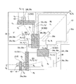
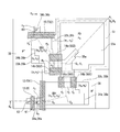
- FIG. 1 is a schematic plan view illustrating an outline of a layout on a semiconductor chip of a solid-state imaging device according to a first embodiment of the present invention. It is a typical top view (top view) explaining the outline of the photoelectric conversion element concerning a 1st embodiment.
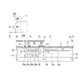
- FIG. 3 is a schematic cross-sectional view illustrating an outline of the photoelectric conversion element according to the first embodiment viewed from a cross section taken along a dashed line in G 0 -G 1 -G 2 -G 3 -G 4 of FIG.
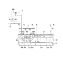
- FIG. 3 is a schematic cross-sectional view illustrating an outline of the photoelectric conversion element according to the first embodiment viewed from a cross section taken along the alternate long and short dash line of H 0 -H 1 -H 2 -H 3 -H 4 in FIG.
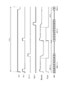
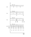
- FIG. 5A is a diagram illustrating the waveform of the first signal charge driving pulse applied to the first select gate electrode of the photoelectric conversion element according to the first embodiment
- FIG. 6 is a diagram for explaining a waveform of a second signal charge driving pulse applied to the second selection gate electrode of the photoelectric conversion element according to the first embodiment for explaining the relationship with FIG.
- FIG. 5C is a timing chart of the output of the first charge accumulation region of the photoelectric conversion element according to the first embodiment for explaining the relationship with FIG.
- FIG. 5A and FIG. These are the timing charts of the output of the 2nd charge storage area
- 6 is a timing chart illustrating a method for reading signal charges in first and second charge storage regions of the photoelectric conversion element according to the first embodiment.
- FIG. 7A is a diagram for explaining a signal charge reading method according to the first comparative example
- FIG. 7B is a second comparative example for explaining the relationship with FIG. 7A.
- FIG. 7C illustrates a signal charge reading method according to a third comparative example for explaining the relationship with FIG. 7A and FIG. 7B.
- FIG. 7D is a diagram for explaining the signal charge reading method of the photoelectric conversion element according to the first embodiment for explaining the relationship with FIG. 7A to FIG. 7C. It is. It is a typical top view (top view) explaining the outline of the photoelectric conversion element which concerns on the modification of 1st Embodiment. It is a typical top view (top view) explaining the outline of the photoelectric conversion element which concerns on the 2nd Embodiment of this invention.
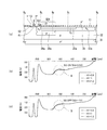
- FIG. 10A is a schematic diagram for explaining an outline of the photoelectric conversion element according to the second embodiment viewed from a cross section taken along the alternate long and short dash line of G 0 -G 1 -G 2 -G 3 -G 4 in FIG. FIG.
- FIG. 10B is a corresponding depletion potential distribution when 3.3 V is applied to the selection gate electrode
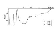
- FIG. 10C is an application of ⁇ 1 V to the selection gate electrode. This is a corresponding depletion potential distribution. It is the elements on larger scale of the area
- FIG. 13A is a schematic diagram for explaining an outline of the photoelectric conversion element according to the second embodiment viewed from a cross section taken along a dashed line of H 0 -H 1 -H 2 -H 3 -H 4 in FIG. FIG.
- FIG. 13B is a corresponding depletion potential distribution when 3.3 V is applied to the selection gate electrode
- FIG. 13C is a case where ⁇ 1 V is applied to the selection gate electrode. This is a corresponding depletion potential distribution.
- FIG. 14A shows the corresponding three-dimensional depletion potential distribution when ⁇ 1V is applied to the selection gate electrode
- FIG. 14B shows the correspondence when 3.3V is applied to the selection gate electrode. This is a three-dimensional depletion potential distribution.
- FIG. 15A is a diagram illustrating the waveform of a signal charge driving pulse applied to the selection gate electrode of the photoelectric conversion element according to the second embodiment
- FIG. 15B is a diagram illustrating FIG. FIG.
- FIG. 15C is a timing chart of the output of the first charge storage region of the photoelectric conversion element according to the second embodiment
- FIG. 15C is a second diagram illustrating the relationship with FIG. It is a timing chart of the output of the 2nd charge storage area
- the regions, members, components, etc. which are defined as the “first conductivity type” or “second conductivity type” and defined as the conductivity type, are all made of semiconductor.
- the conductivity type is selected in the reverse relationship, and the first conductivity type is n-type.
- the second conductivity type may be p-type.
- the solid-state imaging device (two-dimensional image sensor) according to the first embodiment of the present invention includes a pixel array unit (X 11 to X 1m ; X 21 to X 2m ;...; X n1 to It is integrated X nm) and the peripheral circuit portion (104,105,106,107,108) on the same semiconductor chip.
- a horizontal shift register 106 is provided along the pixel rows X 11 to X 1m ; X 21 to X 2m ;... X n1 to X nm on the lower side of the pixel array section.
- a timing generation circuit 104 is connected to the vertical shift register (vertical driver circuit) 105 and the horizontal shift register 106.
- FIG. 7 is a diagram illustrating an example of a planar structure of a pixel that functions as a pixel circuit within each of the pixels X 11 to X 1m ; X 21 to X 2m ;... X n1 to X nm of the solid-state imaging device according to the first embodiment. It is shown in 2.
- a surface-embedded region 33 a that functions as a light-receiving cathode region (charge generation region) is shown as a rectangular region.
- the surface buried region 33a is a second conductivity type (n-type) surface buried region 33a surrounded by the first conductivity type (p-type) base region 32 (see FIGS. 3 and 4).
- the pixel receives an optical signal incident through the aperture portion of the light shielding plate 51, and photoelectrically converts the optical signal into a first signal charge and a second signal charge other than the first signal charge.
- the “first signal charge” is a signal charge whose transfer is controlled by the first selection gate electrode 16 constituting the first path selection mechanism shown in FIG. 2, and the “second signal charge” is the second path selection. This is a signal charge whose transfer is controlled by the second selection gate electrode 14 constituting the mechanism. Details of the definitions of “first signal charge” and “second signal charge” will be described later with reference to FIG.
- the pixel X ij in the pixel array unit is sequentially scanned by the timing generation circuit 104, the horizontal shift register 106, and the vertical shift register (vertical driver circuit) 105 shown in FIG. 1, to the first signal charge and the second signal charge of the pixel signal. Sorting and accumulation, reading after sorting and accumulation, and electronic shutter operation are executed. That is, in the solid-state imaging device according to the first embodiment of the present invention, the first signal charge driving pulse SG1 for driving the first selection gate electrode 16 and the second driving for the second selection gate electrode 14 in one frame.
- the signal charge drive pulse SG2 multiple times complementary, pixel X 11 ⁇ X 1 m of the pixel array unit; transmitting from X n1 ⁇ X nm in the vertical shift register 105; X 21 ⁇ X 2m; .
- the first signal charge is accumulated in the first charge accumulation region (first charge accumulation diode) SD1 shown in FIG. 2 by the first signal charge drive pulse SG1, and the second signal charge is changed by the second signal charge drive pulse SG2.
- the charge is accumulated in the two charge accumulation region (second charge accumulation diode) SD2.
- the pixel array section is scanned in the vertical direction in units of pixel rows X 11 to X 1m ; X 21 to X 2m ;...
- the pixel signals read from the vertical signal lines B 1 , B 2 , B 3 ,..., B j ,..., B m are correlated with the correlated double sampling circuits CDS 1 , CDS 2 , CDS 3 , .., Noise is canceled in CDS m , and AD conversion is performed in analog / digital conversion circuits ADC 1 , ADC 2 , ADC 3 ,..., ADC m of signal processing circuit 108 and then output to horizontal shift register 106. Is done.
- Correlated double sampling circuit CDS1 includes an input capacitor C1 is one electrode to the vertical signal line B 1 is connected, the integral capacitor C2 having one electrode connected to the other electrode of the input capacitor C1, the input capacitance C1 And a differential amplifier 109 having one input terminal connected to the other electrode. The other input terminal of the differential amplifier 109 is grounded. The other electrode of the integration capacitor C ⁇ b> 2 is connected to the output terminal of the differential amplifier 109. In the differential amplifier 109, a switch S1 capable of short-circuiting one input terminal and the output terminal of the differential amplifier 109 is connected in parallel to the differential amplifier 109.
- the correlated double sampling circuits CDS 2 , CDS 3 ,..., CDS m have the same configuration as the correlated double sampling circuit CDS 1 shown in FIG.
- a first selection gate electrode 16 and a second selection gate electrode 14 having an insulated gate structure are arranged on the lower left side of the surface buried region 33a on the planar pattern shown in FIG.
- a two-path selection mechanism is configured.
- a voltage applied to the first selection gate electrode 16 induces a charge transfer channel on the surface of the semiconductor region 32 (see FIG. 3) defining a charge transfer path immediately below the first selection gate electrode 16, so that the pixel
- the generated first signal charge is transferred downward when viewed in the plane pattern shown in FIG.
- a pixel is generated by inducing a charge transfer channel on the surface of a semiconductor region 32 (see FIG. 3) that defines a charge transfer path immediately below the second select gate electrode 14 by a voltage applied to the second select gate electrode 14.
- the second signal charge is transferred in the left direction when viewed in the plane pattern shown in FIG.
- the second conductivity type (n-type) overlaps the lower left region of the surface buried region 33 a and is adjacent to the first selection gate electrode 16 and the second selection gate electrode 14.
- a guide area (internal guide area) 35a is arranged.
- the guide region 35a has a function of guiding the first signal charge and the second signal charge from the surface buried region 33a to the first selection gate electrode 16 and the second selection gate electrode 14 that respectively constitute a path selection mechanism.
- the first charge storage region (charge storage diode) SD1 for temporarily storing the first signal charge transferred by the first select gate electrode 16 has a polygonal shape (in FIG. 2).
- first selection gate electrode 16 are arranged below the first selection gate electrode 16 as a stepped decagon having four steps.
- a first transfer gate electrode 12 adjacent to the first charge accumulation region SD1 and a second opposite to the first charge accumulation region SD1 via the first transfer gate electrode 12 are provided.
- a first charge readout region 61 of a conductivity type (n + type) is arranged.
- first charge readout region 61 On the further left side of the first charge readout region 61, there is provided a reset gate electrode 13 and a reset drain region 62 of the second conductivity type (n + type) facing the first charge readout region 61 via the reset gate electrode 13. Is arranged.
- the first charge readout region 61, the reset gate electrode 13, and the reset drain region 62 form a MOS transistor that serves as a reset transistor. All the control signals R are set to the high (H) level for the respective reset gate electrodes 13, the charges accumulated in the first charge reading region 61 are discharged to the reset drain region 62, respectively, and the first charge reading region 61 is reset. To do.
- a second charge storage region (charge storage diode) SD2 for storing the second signal charge transferred by the second select gate electrode 14 is formed on the left side of the second select gate electrode 14 with a polygon (4 in FIG. 2). It is arranged as a stepped tetragon having stepped steps).
- a second transfer gate electrode 15 adjacent to the second charge accumulation region SD2 and the second charge accumulation region SD2 via the first transfer gate electrode 15 are provided.
- Opposing second charge type (n + type) second charge readout regions 63 are arranged.
- Figure 3 is a G 0 -G 1 -G 2 -G 3 is a cross-sectional structure viewed from a cross-section along the dashed line of -G 4, p + -type semiconductor substrate 31 of the pixel shown in FIG. 2, A p-type base region 32 disposed on the semiconductor substrate 31 by epitaxial growth, an n-type surface buried region 33a selectively buried in a part of the upper portion of the base region 32, and a surface buried region 33a An n-type guide region 35a selectively embedded in a part of the upper portion is shown.
- FIG. 3 illustrates the case where an epitaxial growth substrate in which a p-type substrate region 32 epitaxially grown on the semiconductor substrate 31 is used as the “first conductivity type substrate region”, but instead of using an epitaxial growth substrate.
- a semiconductor substrate of the first conductivity type may be employed as the “first conductivity type substrate region”.
- the surface embedded region 33a is embedded in the upper portion of the base region 32 and functions as a light receiving cathode region (charge generation region).
- the surface buried region 33a and a part of the base region 32 directly below the surface buried region 33a constitute a photodiode PD.
- a part of the substrate region 32 located immediately below the surface buried region 33a functions as a “light receiving anode region (charge generation region)”.
- Carriers (electrons) generated in the light receiving anode region are injected into a part of the surface buried region 33 a immediately above the base region 32.
- a p + type pinning layer 38 is disposed on the surface buried region 33a.
- the p + -type pinning layer 38 is a layer that suppresses the generation of carriers on the surface in the dark, and is used as a preferable layer for reducing dark current. In applications (applications) where dark current is not a problem, the p + -type pinning layer 38 may be omitted from the structure.
- the n-type first well region 34a is spaced apart from the surface buried region 33a and the guide region 35a, and has a polygonal shape as shown in FIG. It arrange
- An n-type first potential gradient forming region 33b is arranged in a part of the upper portion of the first well region 34a corresponding to the polygonal (right-angled octagonal) planar pattern of FIG. 2, and the first potential gradient forming region 33b.
- An n-type first external guide region 35b is arranged on the upper portion of the polygonal pattern so as to overlap the polygonal plane pattern.
- a p-type first embedded accumulation region 36a is arranged corresponding to a polygonal plane pattern.
- a first charge accumulation region SD1 is configured by an overlapping region of the first well region 34a, the first potential gradient forming region 33b, and the first external guide region 35b.
- a first charge reading region 61 and a reset drain region 62 that constitute a reset transistor are disposed in a part of the upper portion of the base region 32.
- the gate insulating film 11 is disposed on the p + type pinning layer 38 and the base region 32.
- the gate insulating film 11 is preferably a silicon oxide film (SiO 2 film), but an insulating gate structure of an insulated gate transistor (MIS transistor) using various insulating films other than the silicon oxide film (SiO 2 film). May be made.
- MIS transistor insulated gate transistor
- an ONO film composed of a three-layered film of silicon oxide film (SiO 2 film) / silicon nitride film (Si 3 N 4 film) / silicon oxide film (SiO 2 film) may be used.
- At least one element of strontium (Sr), aluminum (Al), magnesium (Mg), yttrium (Y), hafnium (Hf), zirconium (Zr), tantalum (Ta), and bismuth (Bi) is contained.
- An oxide containing, silicon nitride containing these elements, or the like can be used as the gate insulating film 11.
- the first selection gate electrode 16 for transferring the first signal charge from the surface buried region 33a to the first charge accumulation region SD1 is disposed on the gate insulating film 11 on the right side of the first charge accumulation region SD1.
- a first transfer gate electrode 12 for transferring the first signal charge from the first charge accumulation region SD1 to the first charge readout region 61 is disposed on the gate insulating film 11 on the left side of the first charge accumulation region SD1.
- a reset gate electrode 13 is disposed on the gate insulating film 11 on the base region 32 on the left side of the first transfer gate electrode 12 so as to be separated from the first transfer gate electrode 12.
- the gate electrode 13 and the reset drain region 62 constitute a reset transistor.
- the first charge readout region 61 is connected to a gate electrode of a signal readout transistor (amplification transistor) MAi constituting the voltage readout buffer amplifier 71.
- the drain electrode of the signal readout transistor (amplification transistor) MAi is connected to the power supply VDD, and the source electrode is connected to the drain electrode of the pixel selection switching transistor MSi.
- the source electrode of the switching transistor MSi for pixel selection is connected to a vertical signal line B j, the selection control signal S is a vertical shift register of the horizontal line to the gate electrode (vertical driver circuit) 105 (see FIG. 1.) Given.
- the selection control signal S When the selection control signal S is set to a high (H) level, the switching transistor MSi is turned on, and a current corresponding to the potential of the first charge accumulation region SD1 amplified by the signal read transistor (amplification transistor) MAi is a vertical signal. Flows on line Bj .
- the impurity density of the base region 32 serving as the charge generation region is lower than the impurity density of the semiconductor substrate 31. That is, the semiconductor substrate 31 has an impurity density of about 4 ⁇ 10 17 cm ⁇ 3 or more and about 1 ⁇ 10 19 cm ⁇ 3 or less, and the base region 32 serving as a charge generation region has an impurity density of about 6 ⁇ 10 11 cm ⁇ 3 or more. About 2 ⁇ 10 16 cm ⁇ 3 or less is preferable.
- the semiconductor substrate 31 is a silicon (Si) substrate having an impurity density of about 4 ⁇ 10 17 cm ⁇ 3 or more and about 5 ⁇ 10 18 cm ⁇ 3 or less, and the base region 32 is an impurity density of about 1 ⁇ 10 12 cm ⁇ 3 or more. If the Si epitaxial growth layer 32 is about 2 ⁇ 10 15 cm ⁇ 3 or less, a normal CMOS process can be adopted.
- the Si substrate 31 having an impurity density of about 8 ⁇ 10 17 cm ⁇ 3 or more and about 3 ⁇ 10 18 cm ⁇ 3 or less, an impurity density of about 1 ⁇ 10 13 cm ⁇ 3 or more, 1.5 ⁇ 10
- a Si epitaxial growth layer 32 of about 15 cm ⁇ 3 or less is preferable because it is easily available on the market.
- the thickness of the Si epitaxial growth layer 32 may be about 4 ⁇ m to 20 ⁇ m, preferably about 6 ⁇ m to 10 ⁇ m.
- the surface embedded region 33a employs an impurity density value of about 1 ⁇ 10 15 cm ⁇ 3 or more and about 1 ⁇ 10 17 cm ⁇ 3 or less, typically about 5 ⁇ 10 16 cm ⁇ 3.
- the thickness can be about 0.1 ⁇ m to 3 ⁇ m, preferably about 0.5 ⁇ m to 1.5 ⁇ m.
- FIG. 4 shows a cross-sectional structure of the pixel as viewed from the cross section along the one-dot chain line of H 0 -H 1 -H 2 -H 3 -H 4 shown in FIG.
- the n-type second well region 34b is arranged corresponding to the polygonal planar pattern of FIG. 2 so as to be separated from the surface buried region 33a and the guide region 35a.
- An n-type second potential gradient forming region 33c is arranged in a part of the upper portion of the second well region 34b corresponding to the polygonal plane pattern of FIG.
- a second outer guide region 35c of the mold is arranged so as to overlap with a polygonal plane pattern.
- a p-type second embedded accumulation region 36b is arranged corresponding to a polygonal plane pattern.
- a second charge accumulation region SD2 is configured by an overlapping region of the second well region 34b, the second potential gradient forming region 33c, and the second external guide region 35c.
- An n-type second charge readout region 63 is disposed on the upper left side of the second well region 34b so as to be separated from the second potential gradient forming region 33c and the second external guide region 35c.
- the voltage reading buffer amplifier 71 is connected to the second charge reading region 63 by connecting to the first charge reading region 61 through a metal wiring, and the first charge storage region SD1 is connected to the first charge storage region SD1.
- the second signal charge accumulated in the second charge accumulation region SD2 is read out in time series independently of reading out the accumulated first signal charge.
- the voltage read buffer amplifier 71 is shared and read in time series.
- another voltage read buffer amplifier different from the voltage read buffer amplifier 71 is connected to the second charge read region 63, and The second signal charge accumulated in the second charge accumulation region SD2 may be read out simultaneously with the reading of the first signal charge accumulated in the first charge accumulation region SD1.
- the second selection gate electrode 14 for transferring the second signal charge from the surface buried region 33a to the second charge accumulation region SD2 is disposed. Furthermore, on the gate insulating film 11 on the left side of the second charge accumulation region SD2, a second transfer gate electrode 15 for transferring the second signal charge from the second charge accumulation region SD2 to the second charge readout region 63 is disposed. Yes.
- FIGS. 5A to 5D show the time in one frame.
- the vertical axis in FIG. 5A indicates a change in the voltage of the first signal charge drive pulse SG1 applied to the first selection gate electrode 16, and the vertical axis in FIG. Shows a change in the voltage of the second signal charge drive pulse SG2 applied to.
- the vertical axis in FIG. 5C indicates the accumulated charge amount of the first signal charge accumulated in the first charge accumulation region SD1, and the vertical axis in FIG. 5B is accumulated in the second charge accumulation region SD2. The accumulated charge amount of the second signal charge.
- the first signal charge driving pulse SG1 and the complementary first signal charge driving pulse SG1 having the phases different from each other with respect to the first selection gate electrode 16 and the second selection gate electrode 14, respectively.
- the two-signal charge driving pulse SG2 By applying the two-signal charge driving pulse SG2, the first signal charge and the second signal charge are alternately distributed to the first charge accumulation region SD1 and the second charge accumulation region SD2.
- the first selection gate electrode 16 is turned on by the first signal charge drive pulse SG1, and the first charge accumulation is performed.
- the first signal charge is transferred to the region SD1, and the first signal charge is stored in the first charge storage region SD1 as shown in FIG.
- the second signal charge drive pulse SG2 turns off the second selection gate electrode 14 in a complementary manner to the first selection gate electrode 16, and the second charge storage region SD2
- the second signal charge is not transferred to, and the second signal charge accumulated in the second charge accumulation region SD2 is constant as shown in FIG. 5C.
- the first select gate electrode 16 is turned off by the first signal charge driving pulse SG1, The first signal charge is not transferred to the first charge accumulation region SD1, and as shown in FIG. 5D, the first signal charge accumulated in the first charge accumulation region SD1 is constant.
- the second selection gate electrode 14 is turned on in a complementary manner to the first selection gate electrode 16 by the second signal charge drive pulse SG2, and the second charge storage region SD2 As shown in FIG. 5C, the second signal charge is stored in the second charge storage region SD2.
- the first signal charge can be defined as the signal charge accumulated in the first charge accumulation region SD1 by the long time exposure shown in FIG.
- the “second signal charge” is a signal charge other than the first signal charge among the signal charges generated by the photoelectric conversion by the photodiode PD, and the second signal charge is generated by the short-time exposure shown in FIG. It can be defined as a signal charge accumulated in the charge accumulation region SD2.
- Complementary combinations of the long exposure at time t0 to t1 and the short exposure at time t1 to t2 are time t2 to t3 and time t3 to t4, time t4 to t5, time t5 to t6, and time t6 in one frame. ... T7 and times t7 to t8 are repeated alternately and periodically.
- FIG. 5 illustrates the case where the complementary combination of long exposure and short exposure is repeated four times, the complementary combination of long exposure and short exposure may be repeated at least twice, You may repeat 5 times or more.
- the first signal charge and the second signal charge accumulated in the first charge accumulation region SD1 and the second charge accumulation region SD2 are read out in time series.
- the control signal TX1 (i) is applied to the first transfer gate electrode 12, and the first signal charge is transferred from the first charge accumulation region SD1 to the first charge readout region 61.
- the potential of the first charge readout region 61 changes, and a high-sensitivity signal from which the fixed pattern noise and reset noise of the pixel Xij are removed appears at the output of the differential amplifier 109.
- the correlated double sampling circuits CDS 1 , CDS 2 , CDS 3 ,..., CDS of the noise cancellation circuit 107 shown in FIG. 1 while maintaining the vertical selection signal S (i) at a high level (Si “1”).
- the AD conversion circuits ADC 1 , ADC 2 , ADC 3 ,..., ADC m of the signal processing circuit 108 are read out during the first half of the period of the horizontal readout period 1H (i) of the i-th row.
- the pixel output corresponding to the signal charge is AD converted and a digital signal SD1 (i) is output.
- the control signal TX2 (i) is applied to the first transfer gate electrode 15, and the second signal charge is transferred from the second charge accumulation region SD2 to the second charge readout region 63.
- the potential of the second charge readout region 63 changes, and the low-sensitivity signal from which the fixed pattern noise of the pixel Xij and the reset noise are removed appears at the output of the differential amplifier 109.
- the AD conversion circuits ADC 1 , ADC 2 , ADC 3 ,..., ADC m of the signal processing circuit 108 are read out in the second half period of the horizontal readout period 1H (i) of the i-th row.
- the pixel output corresponding to the signal charge is AD converted and a digital signal SD2 (i) is output.
- one frame period is divided into a long exposure period L and a short exposure period S, and the accumulated signal of the long exposure period L and the short signal are reduced.
- the sampling window of the short exposure period S becomes smaller than the frame period, and the interval of the short exposure period S is separated by about one frame period.
- one frame period is divided into a long exposure period L, a short exposure period S1, and an ultrashort exposure period S2, and a long exposure period L and a short exposure period S1.
- the sampling window of the short exposure period S1 and the ultrashort exposure period S2 becomes smaller than the frame period, and the interval between the short exposure period S1 and the ultrashort exposure period S2 is almost the same.
- unnatural motion distortion occurs in imaging a fast-moving object because it is separated by one frame period.
- the first signal charge is accumulated in the first charge accumulation region SD1 in the long exposure period L
- the accumulation of the second signal charge in the second charge accumulation region SD2 in the short exposure period S is repeated a plurality of times within one frame.
- a high dynamic range can be obtained by combining the signals of the first charge storage region SD1 and the second charge storage region SD2 having different sensitivities (for example, about 400: 1).
- the two selection mechanisms including the first selection gate electrode 16 and the second selection gate electrode 14 are provided, and the first selection gate electrode 16 and the second selection gate electrode 14 are provided.
- the gate electrode 14 selectively distributes the first signal charge and the second signal charge to the first charge storage region SD1 and the second charge storage region SD2 a plurality of times within one frame.
- the first charge accumulation region SD1 and the second charge accumulation region SD2 are time-divided, and the long exposure period L and the short exposure period S are alternately and repeatedly repeated a plurality of times, and have two sensitivities.
- the photoelectric conversion element according to the modification of the first embodiment of the present invention is replaced with the first selection gate electrode 16 and the second selection gate electrode 14 of the photoelectric conversion element according to the first embodiment shown in FIG. 8, a first path selection mechanism (first electric field control electrode pair) (16a, 16b) and a second path selection mechanism (second electric field control) each composed of a pair of electric field control electrodes.
- the point provided with an electrode pair (14a, 14b) is different from the photoelectric conversion element according to the first embodiment.
- the electric field control electrode (gate electrode) is not disposed immediately above the charge transfer path (channel) through which the first signal charge of the first path selection mechanism (16a, 16b) moves.
- the electric field control electrode (gate electrode) is not disposed immediately above the charge transfer path (channel) through which the second signal charge moves in the second path selection mechanism (14a, 14b). That is, there is no channel in the semiconductor region immediately below the gate electrode (electric field control electrode) constituting the insulated gate structure of the first path selection mechanism (16a, 16b) and the second path selection mechanism (14a, 14b). .
- a channel is not provided in the semiconductor region immediately below the electric field control electrode constituting the first path selection mechanism (16a, 16b) and the second path selection mechanism (14a, 14b), and between the pair of electric field control electrodes.
- a channel is set in the charge transfer path (charge transfer direction) defined in FIG. In such a configuration, for each charge transfer path, the potential and electric field of the charge transfer path (channel) are controlled by an electrostatic induction effect caused by electric lines of force extending in a direction (lateral direction) orthogonal to the charge transfer path.
- each of the first path selection mechanism (16a, 16b) and the second path selection mechanism (14a, 14b) are not arranged immediately above the charge transfer path, The surface potential is not controlled in the vertical direction (vertical direction or depth direction) immediately under the gate electrode as in the gate structure.
- each of the first path selection mechanism (16a, 16b) and the second path selection mechanism (14a, 14b) The electric potential (potential) of the charge transfer path is controlled by the electrostatic induction effect exerted by the electric lines of force extending in the direction according to Gauss's law.
- the photoelectric conversion element according to the modification of the first embodiment shown in FIG. 8 includes two elements, a first path selection mechanism (16a, 16b) and a second path selection mechanism (14a, 14b) using a lateral electric field.
- a route selection mechanism is provided. Therefore, similarly to the timing charts shown in FIGS. 5A to 5D, the first route selection mechanism (16a, 16b) and the second route selection mechanism (14a, 14b) have one frame.
- the first signal charge is transferred to the first charge storage region SD1 and the second signal charge is selectively transferred to the second charge storage region SD2 by using the electrostatic induction effect caused by the lateral electric field. be able to.
- the long exposure period L and the short exposure period S are alternately and repeatedly repeated a plurality of times by time-sharing within one frame, and each of the first signal charge and the second signal charge is changed within one frame. It is possible to repeatedly select and accumulate in the first charge accumulation region SD1 and the second charge accumulation region SD2 a plurality of times, and to read out each of the first signal charge and the second signal charge in time series. Therefore, even with the photoelectric conversion element according to the modification of the first embodiment shown in FIG. 8 and the solid-state imaging device using the photoelectric conversion element, the motion distortion with respect to the object moving at high speed is small and the wide dynamic range image is obtained. It is possible to obtain an effect similar to that of the structure shown in FIGS.
- the overall configuration of the solid-state imaging device (two-dimensional image sensor) according to the second embodiment of the present invention is roughly the same as the configuration shown in FIG.
- An example of a planar structure of a pixel functioning as a pixel circuit within each of the pixels X 11 to X 1m ; X 21 to X 2m ;..; X n1 to X nm of the solid-state imaging device according to the second embodiment 9 shows.
- a surface-embedded region 33 a that functions as a light-receiving cathode region (charge generation region) is shown as a rectangular region.
- the surface buried region 33a is an n type surface buried region 33a selectively buried above the p type substrate region 32.
- the pixel receives an optical signal incident through the opening of the light shielding plate 51, and converts the optical signal into a first signal charge and a second signal charge.
- a selection gate electrode 14 having an insulated gate structure is disposed on the left side of the lower left portion of the rectangular region of the surface buried region 33a so as to function as a path selection mechanism (second path selection mechanism).
- the side path selection mechanism (first path selection mechanism) is not provided with a selection gate electrode that constitutes a normal insulated gate structure. That is, the photoelectric conversion element according to the second embodiment of the present invention has two path selection mechanisms, but only one of the path selection mechanisms is the periphery of the vertical shift register (vertical driver circuit) 105 illustrated in FIG.
- a select gate electrode 14 is driven by the circuit. For this reason, not only the layout in the pixel but also the layout on the semiconductor chip such as the wiring for driving the selection gate electrode is simplified.
- the selection gate electrode 14 constituting the second path selection mechanism which is a direct drive type path selection mechanism, is directly driven by the signal charge driving pulse SG from the peripheral circuit and is generated by the surface buried region 33a.
- the two signal charges are transferred to the second charge accumulation region SD2 and accumulated in the second charge accumulation region SD2.
- the first route selection mechanism is induced by the electrostatic induction effect from the second route selection mechanism, and the change in the potential in the charge transfer route constituting the first route selection mechanism is induced, so that the surface buried region
- This is an indirect drive type path selection mechanism that indirectly controls the movement of the first signal charge generated by 33a (the potential change in the charge movement path will be described later with reference to FIGS. 10 to 13). Therefore, the first path selection mechanism apparently automatically drives the first signal charge from the surface buried region 33a toward the first charge accumulation region SD1 at a specific timing without being driven by the peripheral circuit. Is a route selection mechanism for forwarding to
- the surface buried region 33a is located on the right side of the selection gate electrode 14 via the charge transfer path defined by the relatively narrow widths W1 and W2 and below the charge transfer path. It has a rectangular bowl shape with a rectangular area with a large width.
- the first charge storage region SD1 has a polygonal shape (a right-angled decagon in FIG. 9), and has four steps in a staircase pattern. Thus, it is superimposed on the pattern of the surface embedded region 33a.
- the n-type guide region extends from the lower left to the lower right of the upper right rectangular region of the surface embedded region 33a and overlaps the lower rectangular region of the surface embedded region 33a.
- the region 35a is arranged in a complicated polygonal shape (17-gon in FIG. 9).
- the guide region 35a has a function of guiding the first signal charge from the surface buried region 33a toward the first charge accumulation region SD1 and guiding the second signal charge toward the second charge accumulation region SD2.
- the guide region 35a has a rectangular shape of the surface-embedded region 33a from the lower-left corner of the upper-right rectangular region of the surface-embedded region 33a to the upper-right end of the polygon along the G0-G1 direction (diagonal direction). Projects toward the center of the area.
- the first transfer gate electrode 12 adjacent to the first charge storage region SD1 and the first charge gate electrode 12 facing the first charge storage region SD1 via the first transfer gate electrode 12 are provided.
- a charge readout region 61 is arranged.
- a reset gate electrode 13 and a reset drain region 62 facing the first charge reading region 61 via the reset gate electrode 13 are arranged.
- the first charge readout region 61, the reset gate electrode 13, and the reset drain region 62 form a MOS transistor that serves as a reset transistor. All the control signals R are set to the high (H) level for the respective reset gate electrodes 13, the charges accumulated in the first charge reading region 61 are discharged to the reset drain region 62, respectively, and the first charge reading region 61 is reset. To do.
- the second charge accumulation region SD2 for accumulating the second signal charge transferred by the selection gate electrode 14 is arranged on the left side of the selection gate electrode 14.
- a second transfer gate electrode 15 adjacent to the second charge accumulation region SD2 and the second charge gate region SD2 facing the second charge accumulation region SD2 via the first transfer gate electrode 15 are provided.
- a charge readout region 63 is arranged.
- Figure 10 (a) but is a cross-sectional structure of the pixel as viewed from the G 0 -G 1 -G 2 -G 3 cross-section along the dashed line of -G 4 of the pixel shown in FIG. 9, p + -type semiconductor A substrate 31, a p-type base region 32 disposed on the semiconductor substrate 31, an n-type surface buried region 33a buried in a part of the upper portion of the base region 32, and an upper portion of the surface buried region 33a An n-type guide region 35a embedded in a part of FIG.
- the surface-embedded region 33a is a light-receiving cathode region, which is defined by an opening (aperture portion) of the light shielding plate 51 indicated by a two-dot chain line in FIG. It functions as a (charge generation region).
- a photodiode PD is constituted by the surface buried region 33a and a partial region of the base region 32 that functions as a light receiving anode region directly below the surface buried region 33a. Carriers (electrons) generated in the charge generation region (light-receiving anode region) are injected into a part of the surface buried region 33 a immediately above the base region 32.
- the surface embedding region 33a and the guide region 35a are directed downward from the surface embedding region 33a that defines the periphery of the opening (aperture portion) indicated by a two-dot chain line on the upper right side of FIG. Stretched.
- the surface buried region 33 a and the guide region 35 a extend from the right side to the left side, and the left end overlaps the upper part of the n-type first well region 34 a. ing.
- the p + -type pinning layer 38 is disposed on the surface buried region 33a. However, in applications (applications) where dark current is not a problem, the p + -type pinning layer 38 may be omitted from the structure. I do not care.
- an n-type first well region 34a is arranged above the base region 32 so as to partially overlap the surface buried region 33a and the guide region 35a. Yes.
- a p-type first buried accumulation region 36a is arranged corresponding to the planar pattern of the first well region 34a.
- a first charge accumulation region SD1 is configured by an overlapping region of the first well region 34a, the surface buried region 33a, and the guide region 35a.
- a first charge readout region 61 and a reset drain region 62 constituting a reset transistor are arranged on the left side of the first charge storage diode SD1 and above the base region 32 shown on the left side of FIG. .
- the gate insulating film 11 is disposed on the p + type pinning layer 38 and the base region 32.
- the first transfer gate electrode 12 that transfers the first signal charge from the first charge accumulation region SD1 to the first charge readout region 61 is disposed.
- a reset gate electrode 13 is disposed on the gate insulating film 11 on the base region 32 on the left side of the first well region 34a.
- the first charge readout region 61, the reset gate electrode 13 and the reset drain region 62 A reset transistor is configured.
- a voltage reading buffer amplifier similar to the voltage reading buffer amplifier 71 shown in FIG.
- FIG. 13A shows the cross-sectional structure of the pixel viewed from the cross section along the one-dot chain line of H 0 -H 1 -H 2 -H 3 -H 4 shown in FIG.
- an n-type second well region 34b is disposed so as to be separated from the surface buried region 33a and the guide region 35a.
- An n-type potential gradient forming region 33b is disposed at a part of the upper portion of the second well region 34b, and an n-type external guide region 35b is disposed above the potential gradient forming region 33b.
- a p-type second embedded accumulation region 36b is arranged corresponding to the planar pattern of the second well region 34b.
- a second charge accumulation region SD2 is configured by an overlapping region of the second well region 34b, the potential gradient forming region 33b, and the external guide region 35b.
- An n-type second charge readout region 63 is disposed in a part of the upper portion of the second well region 34b so as to be separated from the potential gradient forming region 33b and the external guide region 35b.
- the second charge readout region 63 is connected to a voltage readout buffer amplifier similar to the voltage readout buffer amplifier 71 shown in FIG.
- the second signal charge accumulated in the second charge accumulation region SD2 is read out in time series independently of the reading of the first signal charge accumulated in SD1.
- a gate electrode 14 is disposed. Further, on the gate insulating film 11 located between the second charge storage region SD2 and the second charge readout region 63 on the planar pattern, which is the position on the left end side of FIG. A second transfer gate electrode 15 for transferring the second signal charge from SD2 to the second charge readout region 63 is disposed.
- the voltage applied to the selection gate electrode 14 constituting the second path selection mechanism shown in FIG. 9 and FIG. 10A is applied from the surface buried region 33a to the first.
- the first signal charge generated by the surface buried area 33a is converted into the first charge accumulation area SD1.
- the second path selection mechanism suppresses the transfer of the second signal charge to the second charge accumulation region SD2, and also the surface buried region 33a.
- the potential barrier in the movement path of the first path selection mechanism from the first charge accumulation area SD1 to the first charge accumulation area SD1 is eliminated, and transfer of the first signal charge to the first charge accumulation area SD1 is allowed.
- the magnitude of the influence of the potential on the second path selection mechanism side on the depletion potential of the movement path on the first path selection mechanism side is the plane of the pixel (photoelectric conversion element) of the solid-state imaging device according to the second embodiment. It depends on the structure of the pattern and the impurity density. For this reason, since a desired potential barrier is not always generated in the movement path of the first path selection mechanism, a signal charge flows through both the first charge accumulation area SD1 and the second charge accumulation area SD2 simultaneously. The “talk” problem may occur. In the following, the dimensions of critical parts for reducing crosstalk between the first charge storage region SD1 and the second charge storage region SD2 will be described.
- the dimension of the critical part of the pixel (photoelectric conversion element) of the solid-state imaging device according to the second embodiment is changed parametrically, and the height of the potential barrier with respect to the first charge accumulation region SD1 and the formation of the potential barrier in the transfer path
- the result of analyzing the presence / absence or the like by device simulation will be described with reference to FIGS.
- the width W1 of the movement path from the end of the selection gate electrode 14 to the end of the guide area 35a shown in FIG. 9 is 0.7 ⁇ m, and is lower than the area having the width W1 of the movement path.
- the width W2 of the region was defined as 0.9 ⁇ m.
- the height H1 on the planar pattern up to the lower side is defined as “path length H1”, and the path length H1 is changed to 0.6 ⁇ m, 1.0 ⁇ m, and 1.3 ⁇ m.
- FIG. 11 shows a partially enlarged view of a region B surrounded by a circle in FIG. 10 (c), and FIG.
- FIG. 12 shows a partially enlarged view of a region A surrounded by a circle in FIG. 10 (b).
- the potential barrier is lowered immediately below the selection gate electrode 14 as shown in FIG.
- a potential barrier is not formed in the charge transfer path of the path selection mechanism and the movement of the first signal charge is allowed. Is formed in the charge transfer path of the first path selection mechanism.
- the selection gate electrode 14 is turned off by the signal charge driving pulse SG, a potential barrier is formed immediately below the selection gate electrode 14 as shown in FIG.
- the path length H1 0.6 ⁇ m, 1.0 ⁇ m, 1 In any case of 3 ⁇ m, no potential barrier is formed in the charge transfer path of the first path selection mechanism, and the movement of the first signal charge is allowed.
- the path length H1 1.3 ⁇ m
- a change in the height of the potential barrier can be induced in the charge transfer path of the first path selection mechanism by the on / off control of the selection gate electrode 14 on the second path selection mechanism side.
- the first signal charge and the second signal charge can be selectively distributed to the first charge accumulation region SD1 and the second charge accumulation region SD2.
- the potential barrier of the charge transfer path of the first path selection mechanism is secured, and the charge transfer path of the first path selection mechanism is
- the height of the potential barrier from the surface buried region 33a along the first charge accumulation region SD1 can be indirectly controlled by the signal charge driving pulse SG applied to the second path selection mechanism side.
- a select gate electrode 14 (denoted as “SG”) corresponding to the depletion potential distribution shown in FIGS.
- FIGS. 14A and 14B the first charge storage region SD1, and the second The positional relationship of charge storage area
- region SD2 is shown typically.
- the X and Y coordinates in FIGS. 14A and 14B correspond to the vertical direction and the horizontal direction in FIG. 9, respectively.
- FIGS. 15A to 15C indicate time in one frame.
- the vertical axis in FIG. 15A indicates the change in the voltage of the signal charge driving pulse SG applied to the selection gate electrode 14 on the second path selection mechanism side
- the vertical axis in FIG. 15B indicates the first charge.
- the accumulated charge amount of the first signal charge accumulated in the accumulation region SD1 is shown
- the vertical axis of FIG. 15C shows the accumulated charge amount of the second signal charge accumulated in the second charge accumulation region SD2.
- the first signal charge is accumulated in the first charge accumulation region SD1 by the long exposure from time t0 to t1
- the second signal charge is accumulated in the second charge accumulation region SD2 by the short exposure from time t1 to t2.
- This complementary combination of long exposure and short exposure is alternately performed at time t2 to t3 and time t3 to t4, time t4 to t5 and time t5 to t6, time t6 to t7 and time t7 to t8 in one frame. Repeat periodically.
- FIGS. 15A to 15C illustrate the operation of repeating the complementary combination of the long exposure and the short exposure four times, but the complementary operation of the long exposure and the short exposure is illustrated.
- the combination may be repeated at least twice, repeated three times, or repeated five or more times. Further, as will be described later as a photoelectric conversion element according to the first modification of the second embodiment, once the movement of the target object is slow and motion distortion does not become a problem, it is once in one frame.
- the repetition mode of is also acceptable.
- the driving method according to the second embodiment of the present invention is a method in which the long exposure period L and the short exposure period S shown in FIG. 7D are repeated a plurality of times within one frame.
- the first signal charge and the second signal charge having two different sensitivity curves are repeatedly generated.
- By accumulating and reading out it is possible to achieve both ultra-high sensitivity and a wide dynamic range, and to acquire images with small motion distortion even for subjects with large movements. It is suitable for an apparatus that is used when the imaging target is high-speed and the light illuminance changes drastically.
- one of the first charge accumulation region SD1 and the second charge accumulation region SD2 is set as a virtual selection gate electrode on the first charge accumulation region SD1 side, and the first charge accumulation region SD1 and the first charge accumulation region SD1 and Since the first signal charge and the second signal charge can be respectively distributed to the second charge accumulation region SD2, the structure of the photoelectric conversion element used as the pixel and the pattern of the surface wiring such as the drive signal line when the pixel is arranged It can be simplified, and an individual imaging device with higher integration density can be provided.
- the case where the driving method of repeating the long exposure period L and the short exposure period S shown in FIG. can also be applied to a conventional driving method. That is, as shown in FIG. 7B, a dual is repeated for each frame, a long exposure section L in which the selection gate electrode 14 is turned on and a short exposure section S in which the selection gate electrode 14 is turned off. Sampling may be performed. Further, as shown in FIG. 7C, a reading method in which one frame is divided into a long exposure period L, a short exposure period S1, and an ultrashort exposure period S2 by controlling the selection gate electrode 14. May be adopted.
- the photoelectric conversion element according to the second modification of the second embodiment of the present invention is as shown in FIG. 16 instead of the selection gate electrode 14 of the photoelectric conversion element according to the second embodiment shown in FIG.
- the photoelectric conversion element according to the second embodiment is different from the photoelectric conversion element according to the second embodiment in that a second path selection mechanism (electric field control electrode pair) (14a, 14b) configured by a pair of electric field control electrodes is provided.
- the electric field control electrode (gate electrode) is not disposed immediately above the charge transfer path (channel) through which the second signal charge of the second path selection mechanism (14a, 14b) moves. That is, there is no channel immediately below the gate electrode that constitutes the insulated gate structure of the second path selection mechanism (14a, 14b). A channel is not provided immediately below the second path selection mechanism (14a, 14b), but a channel is set in a charge transfer path (charge transfer direction) defined between a pair of electric field control electrodes.
- the charge transfer path (by the electrostatic induction effect due to the electric lines of force extending in the direction (lateral direction) orthogonal to the charge transfer path with respect to the charge transfer path of the second path selection mechanism (14a, 14b). Channel) potential and electric field are controlled.
- the surface potential is set in the vertical direction (vertical direction or depth) just below the gate electrode like the gate structure of the conventional MOS transistor. It is not controlled in the direction).
- the photoelectric conversion element according to the second modification of the second embodiment of the present invention shown in FIG. 16 in the second path selection mechanism (14a, 14b), electric lines of force extending in the lateral direction according to Gauss's law are generated.
- the electric potential (potential) of the charge transfer path is controlled by the electrostatic induction effect.
- the photoelectric conversion element according to the second modification example of the second embodiment illustrated in FIG. Although a selection gate electrode that constitutes a normal insulated gate structure is not arranged, the second path selection mechanism (14a, 14b) includes a path selection mechanism using a lateral electric field, and includes two path selection mechanisms. Is configured. As described in the second embodiment, when the second path selection mechanism (14a, 14b) is turned on by the lateral electric field, the first path selection mechanism side is turned off, and the second path is selected. When the selection mechanism (14a, 14b) is turned off by the lateral electric field, the first path selection mechanism side is turned on.
- the drive electric field is applied only to the second path selection mechanism (14a, 14b), and the first signal charge is changed to the first within one frame.
- the second signal charge can be selectively distributed and transferred to the charge storage region SD1 a plurality of times to the second charge storage region SD2.
- the long exposure period L and the short exposure period S are alternately and repeatedly repeated a plurality of times by time-sharing within one frame, and each of the first signal charge and the second signal charge is changed within one frame. It is possible to select and accumulate and read out the first charge accumulation region SD1 and the second charge accumulation region SD2 repeatedly and repeatedly. Therefore, the photoelectric conversion element according to the second modification of the second embodiment shown in FIG. 16 can also obtain a small dynamic distortion and a wide dynamic range image with respect to an object that moves at high speed. It is possible to realize the same effect as the structure shown in (1) with a simple structure.
- the first conductivity type is p-type and the second conductivity type is n-type.
- the first conductivity type is n-type and the second conductivity type is p-type, It can be easily understood that the same effect can be obtained by reversing the electrical polarity.
- the first signal charge and the second signal charge that are transported and accumulated in the photoelectric conversion element are electrons, and in the potential diagram, The depth direction) is the positive direction of the potential (potential).
- the charge to be processed is a hole, so the potential barrier and potential in the photoelectric conversion element In the potential shape indicating the valley, the potential well, and the like, the lower direction (depth direction) of the figure is expressed as a negative direction of the potential.
- the semiconductor material constituting the charge transfer path of the present invention is not limited to silicon (Si).
- Si silicon
- an insulated gate structure as described in the second embodiment of the present invention is used.
- the structure of the non-path selection mechanism can avoid the influence of interface defects and interface states, so that photoelectric conversion elements and solids using various compound semiconductors such as III-V group compound semiconductors and II-VI group compound semiconductors can be used. It is effective for an imaging device. Therefore, the structure and technical idea of the photoelectric conversion element and the solid-state imaging device described as examples in the first and second embodiments are important techniques for the compound semiconductor.
- noise cancellation circuit 108 ... signal processing circuit 109 ... differential amplifier Bj ... vertical signal line C1 ... input capacitance C2 ... integration capacitance MSi ... switching transistors CDS 1 to CDS m ... correlated double sampling circuits ADC 1 to ADC m ... AD converter circuit PD ... photodiodes SD1 and SD2 ... charge storage region (charge storage diode) Xij : Pixel
Landscapes
- Engineering & Computer Science (AREA)
- Multimedia (AREA)
- Signal Processing (AREA)
- Solid State Image Pick-Up Elements (AREA)
- Transforming Light Signals Into Electric Signals (AREA)
Abstract
構造が簡単でダイナミックレンジが広く、且つ高速・高感度な光電変換素子及び固体撮像装置を提供する。第1導電型の基体領域と、基体領域の上部に選択的に埋め込まれ、基体領域とフォトダイオード(PD)をなす第2導電型の表面埋込領域(33a)と、基体領域の上部に埋め込まれ、表面埋込領域(33a)から転送されたフォトダイオード(PD)が生成した第1信号電荷を蓄積する第2導電型の第1電荷蓄積領域(SD1)と、基体領域に埋め込まれ、表面埋込領域(33a)から転送されたフォトダイオード(PD)が生成した第2信号電荷を蓄積する第2導電型の第2電荷蓄積領域(SD2)とを備え、第1の時間で表面埋込領域(33a)から第1電荷蓄積領域(SD1)へ第1信号電荷を転送し、第1の時間よりも短い第2の時間で表面埋込領域(33a)から第2電荷蓄積領域(SD2)へ第2信号電荷を転送することを1フレーム中で複数回繰り返す。
Description
本発明は、光電変換素子、及びこの光電変換素子の複数個を単位画素として配列した固体撮像装置に係り、特に広ダイナミックレンジの光電変換素子及び固体撮像装置に関する。
非常に明るい部分と暗い部分が同時に存在している場合でも、良好な撮像を可能とするためには、広いダイナミックレンジを有した固体撮像装置が必要である。従来、2つのMOSトランジスタを有し、一方のMOSトランジスタの電流増幅度を他方のMOSトランジスタの電流増幅度の10倍とした撮像装置が提案されている(特許文献1参照。)。
特許文献1の装置では、一方のMOSトランジスタを介して蓄積部に蓄積される信号電荷は、他方のMOSトランジスタを介して蓄積部に蓄積される信号電荷の10倍の感度を有することになり、ダイナミックレンジを上げることができる。しかしながら、近年の車載カメラや監視カメラ等の用途においては、動きの速い対象物の撮像が可能な高速なレスポンスと、更なる広いダイナミックレンジを有した高感度な撮像装置が要求されている。
上記問題点に鑑み、本発明は、構造が簡単でダイナミックレンジが広く、且つ動きの速い対象物の撮像が可能な高速なレスポンス特性を有した高感度な光電変換素子及びこの光電変換素子を単位画素として、単位画素を周期的に配列した固体撮像装置を提供することを目的とする。
上記目的を達成するために、本発明の第1の態様は、(a)第1導電型の基体領域と、(b)基体領域の上部に選択的に埋め込まれ、基体領域とフォトダイオードをなす第2導電型の表面埋込領域と、(c)基体領域の上部の表面埋込領域の近傍に埋め込まれ、表面埋込領域から転送されたフォトダイオードが生成した第1信号電荷を蓄積する第2導電型の第1電荷蓄積領域と、(d)第1電荷蓄積領域から離間して、基体領域に埋め込まれ、表面埋込領域から転送されたフォトダイオードが生成した第2信号電荷を蓄積する第2導電型の第2電荷蓄積領域とを備え、第1の時間で表面埋込領域から第1電荷蓄積領域へ第1信号電荷を転送し、第1の時間よりも短い第2の時間で表面埋込領域から第2電荷蓄積領域へ第2信号電荷を転送することを1フレーム中で複数回繰り返す光電変換素子であることを要旨とする。
本発明の第2の態様は、(a)第1導電型の基体領域と、(b)基体領域の上部に選択的に埋め込まれ、基体領域とフォトダイオードをなす第2導電型の表面埋込領域と、(c)基体領域の上部の表面埋込領域の近傍に埋め込まれ、表面埋込領域から転送されたフォトダイオードが生成した第1信号電荷を蓄積する第2導電型の第1電荷蓄積領域と、(d)第1電荷蓄積領域から離間して、基体領域に埋め込まれ、表面埋込領域から転送されたフォトダイオードが生成した第2信号電荷を蓄積する第2導電型の第2電荷蓄積領域とを備える単位画素を複数配列し、単位画素のそれぞれにおいて、第1の時間で表面埋込領域から第1電荷蓄積領域へ第1信号電荷を転送し、第1の時間よりも短い第2の時間で表面埋込領域から第2電荷蓄積領域へ第2信号電荷を転送することを1フレーム中で複数回繰り返す固体撮像装置であることを要旨とする。
本発明によれば、構造が簡単でダイナミックレンジが広く、且つ動きの速い対象物の撮像が可能な高速なレスポンス特性を有した高感度な光電変換素子及びこの光電変換素子を単位画素として、単位画素を周期的に配列した固体撮像装置を提供することができる。
以下に本発明の第1及び第2の実施形態を説明する。以下の図面の記載において、同一又は類似の部分には同一又は類似の符号を付している。但し、図面は模式的なものであり、厚みと平面寸法との関係、各層の厚みの比率等は現実のものとは異なることに留意すべきである。したがって、具体的な厚みや寸法は以下の説明を参酌して判断すべきものである。又、図面相互間においても互いの寸法の関係や比率が異なる部分が含まれていることは勿論である。
以下の第1及び第2の実施形態の説明で「第1導電型」、又は「第2導電型」として修飾して導電型を規定した領域、部材、構成要素等はすべて半導体を材料とする領域、部材、構成要素等である。そして、以下の説明では、第1導電型がp型、第2導電型がn型の場合について例示的に説明するが、導電型を逆の関係に選択して、第1導電型がn型、第2導電型がp型としても構わない。第1導電型がp型、第2導電型がn型の場合は、信号電荷としての多数キャリアは電子となるが、第1導電型がn型、第2導電型がp型の場合は、信号電荷としての多数キャリアは正孔(ホール)となることは、勿論である。又、以下の説明における「左右」や「上下」の方向は、単に説明の便宜上の定義であって、本発明の技術的思想を限定するものではない。よって、例えば、紙面を90度回転すれば「左右」と「上下」は交換して読まれ、紙面を180度回転すれば「左」が「右」に、「右」が「左」になることは勿論である。
(第1の実施形態)
本発明の第1の実施形態に係る固体撮像装置(2次元イメージセンサ)は、図1に示すように、画素アレイ部(X11~X1m;X21~X2m;……;Xn1~Xnm)と周辺回路部(104,105,106,107,108)とを同一の半導体チップ上に集積化している。画素アレイ部には、2次元マトリクス状に多数の画素Xij(i=1~n;j=1~m:m,nはそれぞれ整数である。)が配列されており、方形状の撮像領域を構成している。そして、この画素アレイ部の下辺部には、画素行X11~X1m;X21~X2m;……;Xn1~Xnm方向に沿って水平シフトレジスタ106が設けられ、画素アレイ部の左辺部には画素列X11~Xn1;X12~Xn2;……;X1j~Xnj;……;X1m~Xnm方向に沿って垂直シフトレジスタ(垂直ドライバ回路)105が設けられている。垂直シフトレジスタ(垂直ドライバ回路)105及び水平シフトレジスタ106には、タイミング発生回路104が接続されている。
本発明の第1の実施形態に係る固体撮像装置(2次元イメージセンサ)は、図1に示すように、画素アレイ部(X11~X1m;X21~X2m;……;Xn1~Xnm)と周辺回路部(104,105,106,107,108)とを同一の半導体チップ上に集積化している。画素アレイ部には、2次元マトリクス状に多数の画素Xij(i=1~n;j=1~m:m,nはそれぞれ整数である。)が配列されており、方形状の撮像領域を構成している。そして、この画素アレイ部の下辺部には、画素行X11~X1m;X21~X2m;……;Xn1~Xnm方向に沿って水平シフトレジスタ106が設けられ、画素アレイ部の左辺部には画素列X11~Xn1;X12~Xn2;……;X1j~Xnj;……;X1m~Xnm方向に沿って垂直シフトレジスタ(垂直ドライバ回路)105が設けられている。垂直シフトレジスタ(垂直ドライバ回路)105及び水平シフトレジスタ106には、タイミング発生回路104が接続されている。
第1の実施形態に係る固体撮像装置のそれぞれの画素X11~X1m;X21~X2m;……;Xn1~Xnm内の画素回路として機能する画素の平面構造の一例を、図2に示す。図2の右上側には、受光カソード領域(電荷生成領域)として機能する表面埋込領域33aが矩形状の領域として示されている。表面埋込領域33aは、第1導電型(p型)の基体領域32(図3及び図4参照。)に囲まれた第2導電型(n型)の表面埋込領域33aである。表面埋込領域33aの領域に二点鎖線で示す開口部(アパーチャ部)を開口した遮光板51があり、アパーチャ部以外の画素の領域は遮光板51によってその上方を被覆され、光に対するシールドがなされている。画素は、遮光板51のアパーチャ部を介して入射した光信号を受光し、この光信号を第1信号電荷と第1信号電荷以外の第2信号電荷に光電変換する。「第1信号電荷」は、図2に示した第1経路選択機構を構成する第1選択ゲート電極16によって転送が制御される信号電荷であり、「第2信号電荷」は、第2経路選択機構を構成する第2選択ゲート電極14によって転送が制御される信号電荷である。「第1信号電荷」と「第2信号電荷」の定義の詳細については図5のところで後ほど説明する。
図1に示したタイミング発生回路104、水平シフトレジスタ106及び垂直シフトレジスタ(垂直ドライバ回路)105によって画素アレイ部内の画素Xijが順次走査され、画素信号の第1信号電荷と第2信号電荷への振り分け蓄積、振り分け蓄積後の読み出しや電子シャッタ動作が実行される。即ち、本発明の第1の実施形態に係る固体撮像装置では、1フレーム内において、第1選択ゲート電極16を駆動する第1信号電荷駆動パルスSG1、第2選択ゲート電極14を駆動する第2信号電荷駆動パルスSG2を複数回相補的に、画素アレイ部の画素X11~X1m;X21~X2m;……;Xn1~Xnmに垂直シフトレジスタ105から送信する。第1信号電荷駆動パルスSG1により第1信号電荷が図2に示した第1電荷蓄積領域(第1電荷蓄積ダイオード)SD1に蓄積され、第2信号電荷駆動パルスSG2により、第2信号電荷が第2電荷蓄積領域(第2電荷蓄積ダイオード)SD2に蓄積される。この後、画素アレイ部を各画素行X11~X1m;X21~X2m;……;Xn1~Xnm単位で垂直方向に走査することにより、各画素行X11~X1m;X21~X2m;……;Xn1~Xnmの画素信号を各画素列X11~Xn1;X12~Xn2;……;X1j~Xnj;……;X1m~Xnm毎に設けられた垂直信号線B1,B2,B3,…,Bj,…,Bmによって画素信号を読み出す構成となっている。
各垂直信号線B1,B2,B3,…,Bj,…,Bmから読み出された画素信号は、ノイズキャンセル回路107の相関二重サンプリング回路CDS1,CDS2,CDS3,……,CDSmにおいてノイズがキャンセリングされ、更に信号処理回路108のアナログ・デジタル変換回路ADC1,ADC2,ADC3,……,ADCmにおいてAD変換された後、水平シフトレジスタ106に出力される。相関二重サンプリング回路CDS1は、垂直信号線B1に一方の電極が接続された入力容量C1と、入力容量C1の他方の電極に一方の電極が接続された積分容量C2と、入力容量C1の他方の電極に一方の入力端子が接続された差動アンプ109とを備える。差動アンプ109の他方の入力端子は接地されている。積分容量C2の他方の電極は、差動アンプ109の出力端子に接続されている。差動アンプ109には、差動アンプ109の一方の入力端子と出力端子間を短絡可能なスイッチS1が、差動アンプ109に並列に接続されている。図示を省略するが、相関二重サンプリング回路CDS2,CDS3,……,CDSmも図1に示した相関二重サンプリング回路CDS1と同様の構成を有する。
図2に示す平面パターン上、表面埋込領域33aの左下側には、絶縁ゲート構造を有する第1選択ゲート電極16及び第2選択ゲート電極14が配置され、それぞれが第1経路選択機構及び第2経路選択機構を構成している。第1選択ゲート電極16に印加する電圧により第1選択ゲート電極16の直下に電荷移動経路を定義している半導体領域32(図3参照。)の表面に電荷転送チャネルを誘起して、画素が生成した第1信号電荷を図2に示した平面パターンで見たときの下方向に転送する。第2選択ゲート電極14に印加する電圧により第2選択ゲート電極14の直下に電荷移動経路を定義する半導体領域32(図3参照。)の表面に電荷転送チャネルを誘起して、画素が生成した第2信号電荷を図2に示した平面パターンで見たときの左方向に転送する。
図2に示す平面パターン上、表面埋込領域33aの左下側の領域に重畳し、第1選択ゲート電極16及び第2選択ゲート電極14に隣接するように、第2導電型(n型)のガイド領域(内部ガイド領域)35aが配置されている。ガイド領域35aは、表面埋込領域33aから、それぞれ経路選択機構を構成している第1選択ゲート電極16及び第2選択ゲート電極14へ第1信号電荷及び第2信号電荷をそれぞれ導く機能を有する。図2に示すように、第1選択ゲート電極16により転送された第1信号電荷を一時的に蓄積する第1電荷蓄積領域(電荷蓄積ダイオード)SD1が、平面パターン上、多角形(図2においては、4段のステップを有する階段状10角形)として第1選択ゲート電極16の下側に配置されている。第1電荷蓄積領域SD1の左側には、第1電荷蓄積領域SD1に隣接した第1転送ゲート電極12と、この第1転送ゲート電極12を介して、第1電荷蓄積領域SD1に対向する第2導電型(n+型)の第1電荷読出領域61が配置されている。
第1電荷読出領域61の更に左側には、リセットゲート電極13と、このリセットゲート電極13を介して、第1電荷読出領域61に対向する第2導電型(n+型)のリセットドレイン領域62が配置されている。第1電荷読出領域61、リセットゲート電極13及びリセットドレイン領域62とでリセットトランジスタとなるMOSトランジスタが形成されている。それぞれのリセットゲート電極13に対し、制御信号Rをすべてハイ(H)レベルにして、第1電荷読出領域61に蓄積された電荷をリセットドレイン領域62にそれぞれ吐き出し、第1電荷読出領域61をリセットする。
一方、第2選択ゲート電極14により転送された第2信号電荷を蓄積する第2電荷蓄積領域(電荷蓄積ダイオード)SD2が第2選択ゲート電極14の左側に、多角形(図2においては、4段のステップを有する階段状14角形)として配置されている。平面パターン上、第2電荷蓄積領域SD2の上側には、第2電荷蓄積領域SD2に隣接した第2転送ゲート電極15と、この第1転送ゲート電極15を介して、第2電荷蓄積領域SD2に対向する第2導電型(n+型)の第2電荷読出領域63が配置されている。
図3は、図2に示した画素のG0-G1-G2-G3-G4の一点鎖線に沿った断面から見た断面構造であるが、p+型の半導体基板31と、半導体基板31の上にエピタキシャル成長により配置されたp型の基体領域32と、基体領域32の上部の一部に選択的に埋め込まれたn型の表面埋込領域33aと、表面埋込領域33aの上部の一部に選択的に埋め込まれたn型のガイド領域35aが示されている。
図3では「第1導電型の基体領域」としては、半導体基板31の上にエピタキシャル成長されたp型の基体領域32を形成したエピタキシャル成長基板を用いる場合を例示しているが、エピタキシャル成長基板を用いる代わりに、「第1導電型の基体領域」として第1導電型の半導体基板を採用してもよい。
上述したように、表面埋込領域33aは、基体領域32の上部に埋め込まれており、受光カソード領域(電荷生成領域)として機能する。この表面埋込領域33aと、表面埋込領域33aの直下の基体領域32の一部とでフォトダイオードPDを構成している。表面埋込領域33aの直下に位置した基体領域32の一部が「受光アノード領域(電荷生成領域)」として機能する。受光アノード領域で生成されたキャリア(電子)は、基体領域32の直上の表面埋込領域33aの一部に注入される。
表面埋込領域33aの上には、p+型ピニング層38が配置されている。p+型ピニング層38は、ダーク時の表面でのキャリアの生成を抑制する層であり、ダーク電流削減のために好ましい層として用いている。ダーク電流が問題とならない用途(応用)等では、構造上、p+型ピニング層38を省略しても構わない。
基体領域32の上部の表面埋込領域33a及びガイド領域35aの近傍には、表面埋込領域33a及びガイド領域35aと離間して、n型の第1ウェル領域34aが、図2の多角形の平面パターンに対応して配置されている。第1ウェル領域34aの上部の一部にはn型の第1電位勾配形成領域33bが図2の多角形(直角8角形)の平面パターンに対応して配置され、第1電位勾配形成領域33bの上部にはn型の第1外部ガイド領域35bが多角形の平面パターンに重畳して配置されている。第1ウェル領域34aの底面にはp型の第1埋込蓄積領域36aが多角形の平面パターンに対応して配置されている。第1ウェル領域34aと第1電位勾配形成領域33bと第1外部ガイド領域35bとの重複領域で第1電荷蓄積領域SD1が構成されている。図3の左側に示すように、基体領域32の上部の一部には、リセットトランジスタを構成する第1電荷読出領域61とリセットドレイン領域62が配置されている。
p+型ピニング層38及び基体領域32の上にはゲート絶縁膜11が配置されている。ゲート絶縁膜11としては、シリコン酸化膜(SiO2膜)が好適であるが、シリコン酸化膜(SiO2膜)以外の種々の絶縁膜を用いた絶縁ゲート型トランジスタ(MISトランジスタ)の絶縁ゲート構造をなしてもよい。例えば、シリコン酸化膜(SiO2膜)/シリコン窒化膜(Si3N4膜)/シリコン酸化膜(SiO2膜)の3層積層膜からなるONO膜でも良い。更には、ストロンチウム(Sr)、アルミニウム(Al)、マグネシウム(Mg)、イットリウム(Y)、ハフニウム(Hf)、ジルコニウム(Zr)、タンタル(Ta)、ビスマス(Bi)のいずれか一つの元素を少なくとも含む酸化物、又はこれらの元素を含むシリコン窒化物等がゲート絶縁膜11として使用可能である。
図3において、第1電荷蓄積領域SD1の右側のゲート絶縁膜11上には、表面埋込領域33aから第1電荷蓄積領域SD1へ第1信号電荷を転送する第1選択ゲート電極16が配置されている。又、第1電荷蓄積領域SD1の左側のゲート絶縁膜11上には、第1電荷蓄積領域SD1から第1電荷読出領域61へ第1信号電荷を転送する第1転送ゲート電極12が配置されている。更に、第1転送ゲート電極12の左側の基体領域32上のゲート絶縁膜11上には、第1転送ゲート電極12から離間してリセットゲート電極13が配置され、第1電荷読出領域61、リセットゲート電極13及びリセットドレイン領域62とでリセットトランジスタを構成している。
第1電荷読出領域61には、電圧読出用バッファアンプ71を構成する信号読み出しトランジスタ(増幅トランジスタ)MAiのゲート電極が接続されている。信号読み出しトランジスタ(増幅トランジスタ)MAiのドレイン電極は電源VDDに接続され、ソース電極は画素選択用のスイッチングトランジスタMSiのドレイン電極に接続されている。画素選択用のスイッチングトランジスタMSiのソース電極は、垂直信号線Bjに接続され、ゲート電極には水平ラインの選択用制御信号Sが垂直シフトレジスタ(垂直ドライバ回路)105(図1参照。)から与えられる。選択用制御信号Sをハイ(H)レベルにすることにより、スイッチングトランジスタMSiが導通し、信号読み出しトランジスタ(増幅トランジスタ)MAiで増幅された第1電荷蓄積領域SD1の電位に対応する電流が垂直信号線Bjに流れる。
図3に示した断面構造において、半導体基板31の不純物密度よりも電荷生成領域となる基体領域32の不純物密度の方が低い。即ち、半導体基板31は、不純物密度4×1017cm-3程度以上、1×1019cm-3程度以下、電荷生成領域となる基体領域32が不純物密度6×1011cm-3程度以上、2×1016cm-3程度以下程度が好ましい。特に、半導体基板31を不純物密度4×1017cm-3程度以上、5×1018cm-3程度以下のシリコン(Si)基板、基体領域32を不純物密度1×1012cm-3程度以上、2×1015cm-3程度以下のSiエピタキシャル成長層32とすれば、通常のCMOSプロセスが採用できる。
工業的な意味からは、不純物密度8×1017cm-3程度以上、3×1018cm-3程度以下のSi基板31、不純物密度1×1013cm-3程度以上、1.5×1015cm-3程度以下のSiエピタキシャル成長層32とすれば、市場での入手も容易で好ましい。Siエピタキシャル成長層32の厚さは4μm~20μm程度、好ましくは6μm~10μm程度とすれば良い。表面埋込領域33aは、不純物密度1×1015cm-3程度以上、1×1017cm-3程度以下、代表的には、例えば5×1016cm-3程度の不純物密度の値が採用可能であり、その厚さは0.1μm~3μm程度、好ましくは0.5μm~1.5μm程度とすることが可能である。
図4は、図2に示したH0-H1-H2-H3-H4の一点鎖線に沿った断面から見た画素の断面構造であるが、基体領域32の上部の一部には、表面埋込領域33a及びガイド領域35aと離間するように、n型の第2ウェル領域34bが、図2の多角形の平面パターンに対応して配置されている。第2ウェル領域34bの上部の一部にはn型の第2電位勾配形成領域33cが図2の多角形の平面パターンに対応して配置され、第2電位勾配形成領域33cの上部にはn型の第2外部ガイド領域35cが多角形の平面パターンに重畳して配置されている。第2ウェル領域34bの底面には、p型の第2埋込蓄積領域36bが多角形の平面パターンに対応して配置されている。第2ウェル領域34bと第2電位勾配形成領域33cと第2外部ガイド領域35cとの重複領域で、第2電荷蓄積領域SD2が構成されている。
第2ウェル領域34bの左側の上部には、第2電位勾配形成領域33c及び第2外部ガイド領域35cと離間するように、n型の第2電荷読出領域63が配置されている。図2では図示を省略しているが、メタル配線で第1電荷読出領域61と接続することによって第2電荷読出領域63にも電圧読出用バッファアンプ71を接続し、第1電荷蓄積領域SD1に蓄積された第1信号電荷の読み出しとは独立して時系列に、第2電荷蓄積領域SD2に蓄積された第2信号電荷を読み出す。ここでは電圧読出用バッファアンプ71が共通で時系列に読み出す場合を例示したが、第2電荷読出領域63には、電圧読出用バッファアンプ71とは異なる他の電圧読出用バッファアンプを接続し、第1電荷蓄積領域SD1に蓄積された第1信号電荷の読み出しとは独立に同時に、第2電荷蓄積領域SD2に蓄積された第2信号電荷を読み出してもよい。
第2電荷蓄積領域SD2の右側のゲート絶縁膜11上には、表面埋込領域33aから第2電荷蓄積領域SD2へ第2信号電荷を転送する第2選択ゲート電極14が配置されている。更に、第2電荷蓄積領域SD2の左側のゲート絶縁膜11上には、第2電荷蓄積領域SD2から第2電荷読出領域63へ第2信号電荷を転送する第2転送ゲート電極15が配置されている。
次に、図5(a)~図5(d)のタイミングチャートを参照しながら、本発明の第1の実施形態に係る固体撮像装置における電荷転送動作の一例を説明する。図5(a)~図5(d)の横軸は1フレーム内における時間を示す。図5(a)の縦軸は、第1選択ゲート電極16に印加される第1信号電荷駆動パルスSG1の電圧の変化を示し、図5(b)の縦軸は、第2選択ゲート電極14に印加される第2信号電荷駆動パルスSG2の電圧の変化を示す。図5(c)の縦軸は、第1電荷蓄積領域SD1に蓄積される第1信号電荷の蓄積電荷量を示し、図5(b)の縦軸は、第2電荷蓄積領域SD2に蓄積される第2信号電荷の蓄積電荷量を示す。
図5(a)及び図5(b)に示すように、第1選択ゲート電極16及び第2選択ゲート電極14に対して、それぞれ互いに位相の異なる相補的な第1信号電荷駆動パルスSG1及び第2信号電荷駆動パルスSG2を印加することにより、第1電荷蓄積領域SD1及び第2電荷蓄積領域SD2に第1信号電荷及び第2信号電荷を交互に振り分ける。具体的には、時刻t0~t1(第1の時間)において、図5(a)に示すように、第1信号電荷駆動パルスSG1によって第1選択ゲート電極16がオン状態となり、第1電荷蓄積領域SD1に第1信号電荷を転送し、図5(d)に示すように第1電荷蓄積領域SD1に第1信号電荷が蓄積される。一方、図5(b)に示すように、第2信号電荷駆動パルスSG2によって、第2選択ゲート電極14が、第1選択ゲート電極16とは相補的にオフ状態となり、第2電荷蓄積領域SD2へは第2信号電荷が転送されず、図5(c)に示すように第2電荷蓄積領域SD2に蓄積された第2信号電荷は一定である。
時刻t0~t1よりも短時間の時刻t1~t2(第2の時間)において、図5(a)に示すように、第1信号電荷駆動パルスSG1によって第1選択ゲート電極16がオフ状態となり、第1電荷蓄積領域SD1へ第1信号電荷が転送されず、図5(d)に示すように第1電荷蓄積領域SD1に蓄積された第1信号電荷は一定である。一方、図5(b)に示すように、第2信号電荷駆動パルスSG2によって、第2選択ゲート電極14が、第1選択ゲート電極16とは相補的にオン状態となり、第2電荷蓄積領域SD2に第2信号電荷を転送し、図5(c)に示すように、第2電荷蓄積領域SD2に第2信号電荷が蓄積される。
即ち、第1電荷蓄積領域SD1及び第2電荷蓄積領域SD2にキャリア(光電子)を蓄積するデューティーを変えて、長時間露光により第1電荷蓄積領域SD1に第1信号電荷を蓄積し、短時間露光で第2電荷蓄積領域SD2に第2信号電荷を相補的に蓄積する。即ち、「第1信号電荷」とは、図5(a)に示した長時間露光により第1電荷蓄積領域SD1に蓄積される信号電荷と定義できる。一方、「第2信号電荷」とは、フォトダイオードPDが光電変換により生成した信号電荷の内、第1信号電荷以外の信号電荷であり、図5(b)に示した短時間露光により第2電荷蓄積領域SD2に蓄積される信号電荷である、と定義できる。
時刻t0~t1の長時間露光及び時刻t1~t2の短時間露光の相補的な組み合わせを、1フレーム内の時刻t2~t3と時刻t3~t4、時刻t4~t5と時刻t5~t6、時刻t6~t7と時刻t7~t8で交互且つ周期的に繰り返す。なお、図5では長時間露光及び短時間露光の相補的な組み合わせを4回繰り返す場合を例示しているが、長時間露光及び短時間露光の相補的な組み合わせを少なくとも2回繰り返してもよく、5回以上繰り返してもよい。1フレームの終了する時刻t8において、第1電荷蓄積領域SD1及び第2電荷蓄積領域SD2に蓄積された第1信号電荷及び第2信号電荷をそれぞれ時系列に読み出す。
次に、図6のタイミングチャートを参照して、第1電荷蓄積領域SD1及び第2電荷蓄積領域SD2に蓄積された第1信号電荷及び第2信号電荷の時系列の読み出し方法の一例を説明する。図6では、上から順に、第i行目の画素行Xi1~Ximへの垂直選択信号S(i),リセット信号R(i),第1転送ゲート電極12に印加される制御信号TX1(i),第2転送ゲート電極15に印加される制御信号TX2(i),画素Xijの出力信号,相関二重サンプリング回路CDS1,CDS2,CDS3,……,CDSm内のスイッチS1を制御する制御信号φCDS1,信号処理回路108のAD変換回路ADC1,ADC2,ADC3,……,ADCmによるAD変換後の出力値ADCの時間的変化をそれぞれ示している。
先ず、第i行目の水平読み出し期間1H(i)において、リセット信号R(i)をハイ(H)レベル(Ri=“1”)にして、画素Xij内の第1電荷蓄積領域SD1及び第2電荷蓄積領域SD2の電位をリセットする。更に、図1に示したノイズキャンセル回路107の相関二重サンプリング回路CDS1,CDS2,CDS3,……,CDSmにおいて、スイッチS1を導通状態(閉状態)(φCDS1=“1”)とし、更に垂直選択信号S(i)をハイレベル(Si=“1”)にすることにより、画素Xij内の第1電荷読出領域61及び第2電荷読出領域63のリセット状態の電位レベルを、垂直信号線Bjを介して図1の入力容量C1にサンプルする。このとき、信号処理回路108のAD変換回路ADC1,ADC2,ADC3,……,ADCmは、第(i-1)行目の水平読み出し期間1H(i-1)の後半1/2の期間において読み出された第2信号電荷に対応する画素出力をAD変換し、デジタル信号SD2(i-1)を出力する。
その後、図1に示したノイズキャンセル回路107の相関二重サンプリング回路CDS1,CDS2,CDS3,……,CDSmにおいて、差動アンプ109を増幅モードにする(φCDS1=“0”)。次いで、制御信号TX1(i)を第1転送ゲート電極12に印加し、第1電荷蓄積領域SD1から第1電荷読出領域61へ第1信号電荷を転送する。その結果、第1電荷読出領域61の電位が変化し、差動アンプ109の出力には、画素Xijの固定パターンノイズと、リセットノイズが除去された高感度信号が現れる。
再び、リセット信号R(i)をハイ(H)レベル(Ri=“1”)にして、画素Xij内の第1電荷読出領域61及び第2電荷読出領域63の電位をリセットする。垂直選択信号S(i)をハイレベル(Si=“1”)に維持したまま、図1に示したノイズキャンセル回路107の相関二重サンプリング回路CDS1,CDS2,CDS3,……,CDSmにおいて、スイッチS1を導通状態(閉状態)(φCDS1=“1”)とすることにより、画素Xij内の第1電荷読出領域61及び第2電荷読出領域63のリセット状態の電位レベルを、垂直信号線Bjを介して図1の入力容量C1にサンプルする。信号処理回路108のAD変換回路ADC1,ADC2,ADC3,……,ADCmは、第i行目の水平読み出し期間1H(i)の前半1/2の期間において読み出された第1信号電荷に対応する画素出力をAD変換し、デジタル信号SD1(i)を出力する。
その後、図1に示したノイズキャンセル回路107の相関二重サンプリング回路CDS1,CDS2,CDS3,……,CDSmにおいて、スイッチS1を遮断状態とし、図1の差動アンプ109を増幅モードにする(φCDS1=“0”)。次いで、制御信号TX2(i)を第1転送ゲート電極15に印加し、第2電荷蓄積領域SD2から第2電荷読出領域63へ第2信号電荷を転送する。その結果、第2電荷読出領域63の電位が変化し、差動アンプ109の出力には、画素Xijの固定パターンノイズと、リセットノイズが除去された低感度信号が現れる。信号処理回路108のAD変換回路ADC1,ADC2,ADC3,……,ADCmは、第i行目の水平読み出し期間1H(i)の後半1/2の期間において読み出された第2信号電荷に対応する画素出力をAD変換し、デジタル信号SD2(i)を出力する。
ここで、図7(a)に示すように、従来のイメージセンサの通常の撮影方法では、1フレームの時間Nだけキャリア(光電子)を蓄積して読み出す。このような従来のイメージセンサの読出方法では、光照度が大きくなり1フレームの時間N内で表面埋込領域(受光カソード領域)が飽和してしまうと、白飛びが発生してしまい、それを防ごうと1フレーム内で蓄積時間Nを短くしてしまうと、低照度領域での信号が小さくなり、ノイズに埋もれてしまうため、黒つぶれが発生してしまう。
また、図7(b)に示すように、広いダイナミックレンジを実現するために1フレーム期間を長時間露光期間Lと短時間露光期間Sに分割して、長時間露光期間Lの蓄積信号と短時間露光期間Sの蓄積信号とを合成する手法がある。しかしながら、図7(b)の手法では短時間露光期間Sのサンプリングウインドウがフレーム期間に比して小さくなり、短時間露光期間Sの間隔がほぼ1フレーム期間分隔たるため、動きの速い対象物の撮像で不自然な動き歪が生ずるという問題があった。
また、図7(c)に示すように、1フレーム期間を長時間露光期間L、短時間露光期間S1、超短時間露光期間S2に分割して、長時間露光期間L、短時間露光期間S1、超短時間露光期間S2の異なる信号をそれぞれ読み出して合成する手法がある。図7(c)の手法でも、短時間露光期間S1及び超短時間露光期間S2のサンプリングウインドウがフレーム期間に比して小さくなり、短時間露光期間S1及び超短時間露光期間S2の間隔がほぼ1フレーム期間分隔たるため、動きの速い対象物の撮像で不自然な動き歪が生ずるという問題があった。
これに対して、第1の実施形態に係る固体撮像装置によれば、図7(d)に示すように、長時間露光期間Lにおいて第1電荷蓄積領域SD1に第1信号電荷を蓄積し、短時間露光期間Sにおいて第2電荷蓄積領域SD2に第2信号電荷を蓄積することを1フレーム内で複数回繰り返す。これにより、動きの速い対象物の撮像であっても、隣り合う短時間露光期間Sの間隔が図7(b)及び図7(c)と比較して小さいため、不自然な動き歪が減少すると共に、異なる感度(例えば400:1程度)を持つ第1電荷蓄積領域SD1及び第2電荷蓄積領域SD2の信号を合成することで高ダイナミックレンジが得られる。
以上説明したように、本発明の第1の実施形態によれば、第1選択ゲート電極16及び第2選択ゲート電極14の2つの経路選択機構を備え、第1選択ゲート電極16及び第2選択ゲート電極14が第1電荷蓄積領域SD1及び第2電荷蓄積領域SD2に第1信号電荷及び第2信号電荷を、それぞれ1フレーム内で複数回選択的に振り分ける。その際、第1電荷蓄積領域SD1及び第2電荷蓄積領域SD2を用いて時分割して、長時間露光期間L及び短時間露光期間Sを交互に相補的に複数回繰り返し、2つの感度を持つ信号を1フレーム内で反復的に複数回蓄積して読み出すことで、高速に動く対象物に対する動き歪の小さい広ダイナミックレンジ画像を得ることができる。したがって、自動車のヘッドライトや監視カメラ等の撮像対象が高速であり、且つ光照度が急激に大きく変化する場合に用いられる装置に好適である。
(第1の実施形態の変形例)
本発明の第1の実施形態の変形例に係る光電変換素子は、図2に示した第1の実施形態に係る光電変換素子の第1選択ゲート電極16及び第2選択ゲート電極14の代わりに、図8に示すように、それぞれ1対の電界制御電極のペアによって構成された第1経路選択機構(第1電界制御電極ペア)(16a,16b)及び第2経路選択機構(第2電界制御電極ペア)(14a,14b)を備える点が、第1の実施形態に係る光電変換素子と異なる。
本発明の第1の実施形態の変形例に係る光電変換素子は、図2に示した第1の実施形態に係る光電変換素子の第1選択ゲート電極16及び第2選択ゲート電極14の代わりに、図8に示すように、それぞれ1対の電界制御電極のペアによって構成された第1経路選択機構(第1電界制御電極ペア)(16a,16b)及び第2経路選択機構(第2電界制御電極ペア)(14a,14b)を備える点が、第1の実施形態に係る光電変換素子と異なる。
図8から分かるように、第1経路選択機構(16a,16b)の第1信号電荷が移動する電荷移動経路(チャネル)の直上には電界制御電極(ゲート電極)が配置されていない。同様に、第2経路選択機構(14a,14b)の第2信号電荷が移動する電荷移動経路(チャネル)の直上には電界制御電極(ゲート電極)が配置されていない。即ち、第1経路選択機構(16a,16b)及び第2経路選択機構(14a,14b)の絶縁ゲート構造を構成しているゲート電極(電界制御電極)の直下の半導体領域にはチャネルが存在しない。第1経路選択機構(16a,16b)及び第2経路選択機構(14a,14b)を構成している電界制御電極の直下の半導体領域にチャネルを設けず、1対の電界制御電極のペアの間に定義される電荷移動経路(電荷転送方向)にチャネルが設定されている。このような構成において、それぞれの電荷移動経路に対し、電荷移動経路に直交する方向(横方向)に伸びる電気力線による静電誘導効果によって、電荷移動経路(チャネル)のポテンシャル及び電界が制御される。
第1経路選択機構(16a,16b)及び第2経路選択機構(14a,14b)のそれぞれを構成している電界制御電極は、電荷移動経路の直上に配置されていないので、従来のMOSトランジスタのゲート構造のようなゲート電極直下において、表面ポテンシャルを縦方向(垂直方向又は深さ方向)に制御するのではない。図8に示した本発明の第1の実施形態の変形例に係る光電変換素子においては、第1経路選択機構(16a,16b)及び第2経路選択機構(14a,14b)において、それぞれの横方向にガウスの法則に従って伸びる電気力線が及ぼす静電誘導効果により、電荷移動経路の電位(ポテンシャル)をそれぞれ制御する。横方向電界による静電誘導効果を用いることにより、電荷転送方向の長い距離にわたって電界がほぼ一定になるようにして、第1信号電荷及び第2信号電荷をそれぞれ転送する光電変換素子を実現できる。
図8に示した第1の実施形態の変形例に係る光電変換素子は、横方向電界を用いた第1経路選択機構(16a,16b)及び第2経路選択機構(14a,14b)の2つの経路選択機構を備えている。このため、図5(a)~図5(d)のタイミングチャートに示したのと同様に、第1経路選択機構(16a,16b)及び第2経路選択機構(14a,14b)が、1フレーム内で、横方向電界による静電誘導効果を用いて、第1信号電荷を第1電荷蓄積領域SD1に、第2信号電荷を第2電荷蓄積領域SD2に、複数回選択的に振り分けて転送することができる。その際、1フレーム内を時分割して、長時間露光期間L及び短時間露光期間Sを交互に相補的に複数回繰り返し、第1信号電荷及び第2信号電荷のそれぞれを、1フレーム内で反復的に複数回、第1電荷蓄積領域SD1及び第2電荷蓄積領域SD2に選択して蓄積し、第1信号電荷及び第2信号電荷のそれぞれを時系列に読み出すことが可能である。よって、図8に示した第1の実施形態の変形例に係る光電変換素子及びこの光電変換素子を用いた固体撮像装置によっても、高速に動く対象物に対する動き歪の小さく、且つ広ダイナミックレンジ画像を得ることができるという図2~図4等に示した構造と同様な効果を奏することが可能である。
(第2の実施形態)
本発明の第2の実施形態に係る固体撮像装置(2次元イメージセンサ)の半導体チップ上の配置等の全体構成は、概略としては図1に示した構成と同様である。第2の実施形態に係る固体撮像装置のそれぞれの画素X11~X1m;X21~X2m;……;Xn1~Xnm内の画素回路として機能する画素の平面構造の一例を、図9に示す。図9の右上側には、受光カソード領域(電荷生成領域)として機能する表面埋込領域33aが矩形状の領域として示されている。表面埋込領域33aは、p型の基体領域32の上部に選択的に埋め込まれたn型の表面埋込領域33aである。画素は、遮光板51の開口部を介して入射した光信号を受光し、この光信号を第1信号電荷及び第2信号電荷に変換する。
本発明の第2の実施形態に係る固体撮像装置(2次元イメージセンサ)の半導体チップ上の配置等の全体構成は、概略としては図1に示した構成と同様である。第2の実施形態に係る固体撮像装置のそれぞれの画素X11~X1m;X21~X2m;……;Xn1~Xnm内の画素回路として機能する画素の平面構造の一例を、図9に示す。図9の右上側には、受光カソード領域(電荷生成領域)として機能する表面埋込領域33aが矩形状の領域として示されている。表面埋込領域33aは、p型の基体領域32の上部に選択的に埋め込まれたn型の表面埋込領域33aである。画素は、遮光板51の開口部を介して入射した光信号を受光し、この光信号を第1信号電荷及び第2信号電荷に変換する。
表面埋込領域33aの矩形状の領域の左下部分の左側には、経路選択機構(第2経路選択機構)として機能するように、絶縁ゲート構造の選択ゲート電極14が配置されているが、下側の経路選択機構(第1経路選択機構)には、通常の絶縁ゲート構造を構成するような選択ゲート電極は配置されていない。即ち、本発明の第2の実施形態に係る光電変換素子は、2つの経路選択機構を有するが、一方の経路選択機構のみが図1に例示した垂直シフトレジスタ(垂直ドライバ回路)105等の周辺回路によって駆動される選択ゲート電極14を有する。このため、画素内のレイアウトだけでなく、選択ゲート電極を駆動する配線等の半導体チップ上のレイアウトが簡略化されている。
直接駆動型経路選択機構である第2経路選択機構を構成している選択ゲート電極14は、周辺回路からの信号電荷駆動パルスSGによって直接的に駆動されて、表面埋込領域33aにより生成した第2信号電荷を第2電荷蓄積領域SD2に転送して、第2電荷蓄積領域SD2に蓄積する。これに対し第1経路選択機構は、第2経路選択機構からの静電誘導効果で、第1経路選択機構を構成している電荷移動経路内の電位の変化が誘導されて、表面埋込領域33aが生成した第1信号電荷の移動を、間接的に制御する間接駆動型経路選択機構である(電荷移動経路内の電位の変化については、図10~図13を用いて後述する。)。このため、第1経路選択機構は、周辺回路によって駆動されることなく、第1信号電荷を、特定のタイミングで、表面埋込領域33aから第1電荷蓄積領域SD1に向かって、見かけ上自動的に転送する経路選択機構である。
図9に示した平面パターン上、表面埋込領域33aは、選択ゲート電極14の右側を比較的細い幅W1,W2で規定される電荷移動経路を経由して、下側に電荷移動経路よりも太い幅となる矩形状の領域を有した、矩形瓢箪型をなしている。表面埋込領域33aの左下側の矩形状の領域の一部には、第1電荷蓄積領域SD1が多角形(図9においては直角10角形)の形で、階段状に4段のステップを有して表面埋込領域33aのパターンに重畳している。又、表面埋込領域33aの右上の矩形領域の左下から下側に向かって延在し、表面埋込領域33aの下側の矩形の領域と重畳するように、n型のガイド領域(貫通ガイド領域)35aが複雑な多角形(図9においては17角形)の形状で配置されている。ガイド領域35aは、表面埋込領域33aから第1電荷蓄積領域SD1の方向へ第1信号電荷を導き、第2電荷蓄積領域SD2の方向へ第2信号電荷を導く機能を有する。ガイド領域35aは、表面埋込領域33aの右上の矩形状の領域の左下から、多角形の右上側の先端部が、G0―G1方向(対角線方向)に沿って表面埋込領域33aの矩形状の領域の中央部に向かい突出している。
第1電荷蓄積領域SD1の左側には、第1電荷蓄積領域SD1に隣接した第1転送ゲート電極12と、この第1転送ゲート電極12を介して、第1電荷蓄積領域SD1に対向する第1電荷読出領域61が配置されている。第1電荷読出領域61の更に左側には、リセットゲート電極13と、このリセットゲート電極13を介して、第1電荷読出領域61に対向するリセットドレイン領域62が配置されている。第1電荷読出領域61、リセットゲート電極13及びリセットドレイン領域62とでリセットトランジスタとなるMOSトランジスタが形成されている。それぞれのリセットゲート電極13に対し、制御信号Rをすべてハイ(H)レベルにして、第1電荷読出領域61に蓄積された電荷をリセットドレイン領域62にそれぞれ吐き出し、第1電荷読出領域61をリセットする。
一方、選択ゲート電極14により転送された第2信号電荷を蓄積する第2電荷蓄積領域SD2が選択ゲート電極14の左側に配置されている。第2電荷蓄積領域SD2の上側には、第2電荷蓄積領域SD2に隣接した第2転送ゲート電極15と、この第1転送ゲート電極15を介して、第2電荷蓄積領域SD2に対向する第2電荷読出領域63が配置されている。
図10(a)は図9に示した画素のG0-G1-G2-G3-G4の一点鎖線に沿った断面から見た画素の断面構造であるが、p+型の半導体基板31と、半導体基板31の上に配置されたp型の基体領域32と、基体領域32の上部の一部に埋め込まれたn型の表面埋込領域33aと、表面埋込領域33aの上部の一部に埋め込まれたn型のガイド領域35aが示されている。
表面埋込領域33aは、図9において二点鎖線で示す遮光板51の開口部(アパーチャ部)に定義される、基体領域32の上部の一部に埋め込まれた矩形状の領域が受光カソード領域(電荷生成領域)として機能する。表面埋込領域33aと、表面埋込領域33aの直下の受光アノード領域として機能する基体領域32の一部の領域とでフォトダイオードPDを構成している。電荷生成領域(受光アノード領域)で生成されたキャリア(電子)は、基体領域32の直上の表面埋込領域33aの一部に注入される。表面埋込領域33a及びガイド領域35aは、図9の右上側に二点鎖線で示した開口部(アパーチャ部)の周辺を画定している表面埋込領域33aから、平面パターン上、下方に向かって延伸している。図9に対応して、図10(a)では表面埋込領域33a及びガイド領域35aは右側から左側に向かって延伸し、左側の端部がn型の第1ウェル領域34aの上部と重畳している。
表面埋込領域33aの上には、p+型ピニング層38が配置されているが、ダーク電流が問題とならない用途(応用)等では、構造上、p+型ピニング層38を省略しても構わない。図10(a)の左側に示すように、基体領域32の上部には、表面埋込領域33a及びガイド領域35aと一部が重複するように、n型の第1ウェル領域34aが配置されている。第1ウェル領域34aの底面にはp型の第1埋込蓄積領域36aが第1ウェル領域34aの平面パターンに対応して配置されている。第1ウェル領域34aと表面埋込領域33aとガイド領域35aとの重複領域で第1電荷蓄積領域SD1を構成している。第1電荷蓄積ダイオードSD1の左側となる、図10(a)の左側に示した基体領域32の上部には、リセットトランジスタを構成する第1電荷読出領域61とリセットドレイン領域62が配置されている。
p+型ピニング層38及び基体領域32の上にはゲート絶縁膜11が配置されている。第1ウェル領域34aの左側のゲート絶縁膜11上には、第1電荷蓄積領域SD1から第1電荷読出領域61へ第1信号電荷を転送する第1転送ゲート電極12が配置されている。又、第1ウェル領域34aの左方となる基体領域32上のゲート絶縁膜11上にはリセットゲート電極13が配置され、第1電荷読出領域61、リセットゲート電極13及びリセットドレイン領域62とでリセットトランジスタを構成している。図10(a)では図示を省略するが、第1電荷読出領域61には、図3に示した電圧読出用バッファアンプ71と同様の電圧読出用バッファアンプが接続されている。
図13(a)は、図9に示したH0-H1-H2-H3-H4の一点鎖線に沿った断面から見た画素の断面構造であるが、基体領域32の上部の一部には、表面埋込領域33a及びガイド領域35aと離間するように、n型の第2ウェル領域34bが配置されている。第2ウェル領域34bの上部の一部にはn型の電位勾配形成領域33bが配置され、電位勾配形成領域33bの上部にはn型の外部ガイド領域35bが配置されている。第2ウェル領域34bの底面にはp型の第2埋込蓄積領域36bが第2ウェル領域34bの平面パターンに対応して配置されている。第2ウェル領域34bと電位勾配形成領域33bと外部ガイド領域35bとの重複領域で第2電荷蓄積領域SD2を構成している。
第2ウェル領域34bの上部の一部には、電位勾配形成領域33b及び外部ガイド領域35bと離間するように、n型の第2電荷読出領域63が配置されている。図13(a)では図示を省略するが、第2電荷読出領域63には、図4に示した電圧読出用バッファアンプ71と同様の電圧読出用バッファアンプを接続して、第1電荷蓄積領域SD1に蓄積された第1信号電荷の読み出しとは独立して時系列に、第2電荷蓄積領域SD2に蓄積された第2信号電荷を読み出す。
平面パターン上、表面埋込領域33aと第2電荷蓄積領域SD2の間に位置するゲート絶縁膜11上には、表面埋込領域33aから第2電荷蓄積領域SD2へ第2信号電荷を転送する選択ゲート電極14が配置されている。更に、図13(a)の左端側の位置となる、平面パターン上、第2電荷蓄積領域SD2と第2電荷読出領域63の間に位置するゲート絶縁膜11上には、第2電荷蓄積領域SD2から第2電荷読出領域63へ第2信号電荷を転送する第2転送ゲート電極15が配置されている。
本発明の第2の実施形態においては、図9及び図10(a)に示した第2経路選択機構を構成している選択ゲート電極14に印加する電圧が、表面埋込領域33aから第1電荷蓄積領域SD1までの、第1経路選択機構を構成している移動経路における空乏化電位の変化を誘導することにより、表面埋込領域33aにより生成した第1信号電荷を第1電荷蓄積領域SD1に見かけ上自動的に転送させる。即ち、第2経路選択機構としての選択ゲート電極14がオン状態のときは、第2電荷蓄積領域SD2に第2信号電荷を転送するとともに、第1経路選択機構側においては、表面埋込領域33aから第1電荷蓄積領域SD1までの移動経路における電位障壁を見かけ上自動的に形成して第1電荷蓄積領域SD1への第1信号電荷の転送を抑制する。一方、第2経路選択機構である選択ゲート電極14がオフ状態のときは、第2経路選択機構は第2電荷蓄積領域SD2への第2信号電荷の転送を抑制するとともに、表面埋込領域33aから第1電荷蓄積領域SD1までの第1経路選択機構の移動経路における電位障壁をなくして、第1電荷蓄積領域SD1への第1信号電荷の転送を許容する。
第2経路選択機構側の電位が、第1経路選択機構側の移動経路の空乏化電位に与える影響の大きさは、第2の実施形態に係る固体撮像装置の画素(光電変換素子)の平面パターン等の構造や不純物密度に依存する。このため、常には、所望の電位障壁が第1経路選択機構の移動経路に生成されないので、第1電荷蓄積領域SD1、第2電荷蓄積領域SD2の両方に、同時に信号電荷が流れてしまう「クロストーク」の問題が発生する場合もある。以下においては、第1電荷蓄積領域SD1、第2電荷蓄積領域SD2の間のクロストークを低減するうえで、クリティカルな部分の寸法について説明する。
第2の実施形態に係る固体撮像装置の画素(光電変換素子)のクリティカルな部分の寸法を、パラメトリックに変化させ、第1電荷蓄積領域SD1に対する電位障壁の高さ、転送路における電位障壁の形成の有無等をデバイスシミュレーションで解析した結果を図10~図13を用いて説明する。クリティカルな部分の寸法として、図9に示す選択ゲート電極14の端部からガイド領域35aの端部までの移動経路の幅W1を0.7μm、移動経路の幅W1を有する領域よりも下側の領域の幅W2を0.9μmと規定した。表面埋込領域33aの瓢箪の胴のくびれ部分となる箇所の長さ、即ち、図9において、下側の矩形状の表面埋込領域33aの上辺から、上側の矩形状の表面埋込領域33aの下辺までの平面パターン上の高さH1を「経路長H1」と定義し、経路長H1を0.6μm、1.0μm、1.3μmと変化させた。
図10(b)は、選択ゲート電極14に信号電荷駆動パルスSG=3.3Vを印加して第2経路選択機構をオン状態としたときの図10(a)に対応する断面に沿った第1経路選択機構の電荷移動経路の空乏化電位分布のシミュレーション結果を示し、図10(c)は、選択ゲート電極14に信号電荷駆動パルスSG=-1Vを印加して第2経路選択機構をオフ状態としたときの図10(a)に対応する断面に沿った第1経路選択機構の電荷移動経路の空乏化電位分布のシミュレーション結果を示す。図11に、図10(c)の円で囲んだ領域Bの部分拡大図を示し、図12に、図10(b)の円で囲んだ領域Aの部分拡大図を示す。図13(b)は、選択ゲート電極14に信号電荷駆動パルスSG=3.3Vを印加して第2経路選択機構をオン状態としたときの図13(a)に対応する断面に沿った第2経路選択機構の電荷移動経路の空乏化電位分布のシミュレーション結果を示し、図13(c)は、選択ゲート電極14に信号電荷駆動パルスSG=-1Vを印加して第2経路選択機構をオフ状態としたときの図13(a)に対応する断面に沿った第2経路選択機構の電荷移動経路の空乏化電位分布のシミュレーション結果を示す。
選択ゲート電極14を信号電荷駆動パルスSGによってオン状態としたときに、図13(b)に示すように、選択ゲート電極14直下では電位障壁が下がる。同時に、図10(b)及び図12に示すように、表面埋込領域33aと第1電荷蓄積領域SD1の間のガイド領域35aの部分において、経路長H1=0.6μmの場合には第1経路選択機構の電荷移動経路に電位障壁が形成されず、第1信号電荷の移動を許容するが、経路長H1=1.0μm,1.3μmの場合には第1電荷蓄積領域SD1に対する1V以上の電位障壁が第1経路選択機構の電荷移動経路に形成される。
一方、選択ゲート電極14を信号電荷駆動パルスSGによってオフ状態としたときに、図13(c)に示すように、選択ゲート電極14直下には電位障壁が形成される。同時に、図10(c)及び図11に示すように、表面埋込領域33aと第1電荷蓄積領域SD1の間のガイド領域35aの部分において、経路長H1=0.6μm、1.0μm、1.3μmのいずれの場合も第1経路選択機構の電荷移動経路に電位障壁が形成されず、第1信号電荷の移動を許容する。
したがって、経路長H1=1.3μmの場合には、第2経路選択機構側の選択ゲート電極14のオンオフ制御により、第1経路選択機構の電荷移動経路に電位障壁の高さの変化を誘導でき、第1電荷蓄積領域SD1及び第2電荷蓄積領域SD2に第1信号電荷及び第2信号電荷を選択的に振り分けることができる。このように、電荷移動経路中に定義される転送路の経路長H1を確保することで、第1経路選択機構の電荷移動経路の電位障壁が確保され、第1経路選択機構の電荷移動経路に沿った表面埋込領域33aから第1電荷蓄積領域SD1への電位障壁の高さを、第2経路選択機構側に印加する信号電荷駆動パルスSGによって、間接的に制御することができる。
更に、図14(a)に、選択ゲート電極14に信号電荷駆動パルスSG=-1Vを印加して第2経路選択機構をオフ状態としたときの第1及び第2経路選択機構の電荷移動経路の空乏化電位分布の3次元シミュレーション結果を示し、図14(b)に、選択ゲート電極14に信号電荷駆動パルスSG=3.3Vを印加して第2経路選択機構をオン状態としたときの第1及び第2経路選択機構の電荷移動経路の空乏化電位分布の3次元シミュレーション結果を示す。図14(a)の右上に、図14(a)及び図14(b)に示す空乏化電位分布に対応する選択ゲート電極14(「SG」と表記)、第1電荷蓄積領域SD1及び第2電荷蓄積領域SD2の位置関係を模式的に示す。図14(a)及び図14(b)のX座標及びY座標は、図9の紙面上下方向及び紙面左右方向にそれぞれ対応する。
図14(a)に示すように、選択ゲート電極14に信号電荷駆動パルスSG=-1Vを印加して第2経路選択機構をオフ状態としたときには、選択ゲート電極14直下には電位障壁が形成されると同時に、第1経路選択機構の電荷移動経路に電位障壁が形成されず、第1信号電荷の移動を許容する。一方、図14(b)に示すように、選択ゲート電極14に信号電荷駆動パルスSG=3.3Vを印加して第2経路選択機構をオン状態としたときには、選択ゲート電極14直下では電位障壁が下がると同時に、第1経路選択機構の電荷移動経路には電位障壁が形成される。
次に、図15(a)~図15(c)のタイミングチャートを参照しながら、本発明の第2の実施形態に係る固体撮像装置における電荷転送動作の一例を説明する。図15(a)~図15(c)の横軸は1フレーム内における時間を示す。図15(a)の縦軸は、第2経路選択機構側の選択ゲート電極14に印加される信号電荷駆動パルスSGの電圧の変化を示し、図15(b)の縦軸は、第1電荷蓄積領域SD1に蓄積される第1信号電荷の蓄積電荷量を示し、図15(c)の縦軸は、第2電荷蓄積領域SD2に蓄積される第2信号電荷の蓄積電荷量を示す。
時刻t0~t1において、図15(a)に示すように、第2経路選択機構側の選択ゲート電極14が信号電荷駆動パルスSGによってオフ状態となると、第2電荷蓄積領域SD2への第2信号電荷の転送は抑制され、図15(b)に示すように第2電荷蓄積領域SD2に蓄積された第2信号電荷は一定である。一方、第1経路選択機構側の第1電荷蓄積領域SD1への第1信号電荷の転送は許容されて、図15(c)に示すように、第1電荷蓄積領域SD1に第1信号電荷が蓄積される。
時刻t0~t1よりも短時間の時刻t1~t2において、図15(a)に示すように、第2経路選択機構側の選択ゲート電極14が信号電荷駆動パルスSGによってオン状態となると、第2電荷蓄積領域SD2に第2信号電荷が転送され、図15(b)に示すように、第2電荷蓄積領域SD2に第2信号電荷が蓄積される。一方、第1経路選択機構側の第1電荷蓄積領域SD1への第1信号電荷の転送は抑制され、図15(c)に示すように第1電荷蓄積領域SD1に蓄積された第1信号電荷は一定である。
即ち、時刻t0~t1の長時間露光で第1電荷蓄積領域SD1に第1信号電荷を蓄積し、時刻t1~t2の短時間露光で第2電荷蓄積領域SD2に第2信号電荷を蓄積する。この長時間露光と短時間露光の相補的な組み合わせを1フレーム内の時刻t2~t3と時刻t3~t4、時刻t4~t5と時刻t5~t6、時刻t6~t7と時刻t7~t8で交互且つ周期的に繰り返す。なお、図15(a)~図15(c)では、長時間露光と短時間露光の相補的な組み合わせを4回繰り返す動作を例示しているが、長時間露光と短時間露光の相補的な組み合わせは少なくとも2回繰り返してもよく、3回繰り返してもよく、5回以上繰り返してもよい。又、第2の実施形態の第1の変形例に係る光電変換素子として後述するように、対象物の動作が遅い場合で、動き歪が問題にならない状況であれば、1フレーム内に1回の繰り返しのモードも許容しうる。
1フレームの終了する時刻t8において、第1電荷蓄積領域SD1に蓄積された第1信号電荷と、第2電荷蓄積領域SD2に蓄積された第2信号電荷とを時系列で読み出す。即ち、本発明の第2の実施形態に係る駆動方法は、図7(d)に示した長時間露光期間L及び短時間露光期間Sを1フレーム内で複数回繰り返す手法である。
本発明の第2の実施形態によれば、第1電荷蓄積領域SD1及び第2電荷蓄積領域SD2を用いて、異なる2つの感度曲線を持つ第1信号電荷と第2信号電荷を、反復的に蓄積して読み出すことで、超高感度と広ダイナミックレンジを両立し、さらに、動きの大きい被写体に対しても合成画像の動き歪が小さい画像を取得できるしたがって、自動車のヘッドライトや監視カメラ等の撮像対象が高速であり、且つ光照度が急激に大きく変化する場合に用いられる装置に好適である。
更に、第1電荷蓄積領域SD1及び第2電荷蓄積領域SD2のうち、一方の第1電荷蓄積領域SD1側を仮想的な選択ゲート電極とし、1つの選択ゲート電極14により第1電荷蓄積領域SD1及び第2電荷蓄積領域SD2へ第1信号電荷及び第2信号電荷をそれぞれ振り分けることができるので、画素として用いる光電変換素子の構造や、画素を配列したときの駆動信号線等の表面配線のパターンを簡略化でき、より高集積密度の個体撮像素子を提供できる。
(第2の実施形態の第1の変形例)
本発明の第2の実施形態においては、図7(d)に示した長時間露光期間L及び短時間露光期間Sを複数回繰り返す駆動方法を採用する場合を例示したが、本発明の第2の実施形態に係る光電変換素子及び固体撮像装置を、従来の駆動方法に適用することもできる。即ち、図7(b)に示すように、1フレーム毎に、選択ゲート電極14のオン状態とした長時間露光区間Lと、選択ゲート電極14をオフ状態とした短時間露光区間Sを繰り返すデュアルサンプリングを実施してもよい。更には、図7(c)に示すように、選択ゲート電極14を制御することにより、1フレーム中を長時間露光期間L、短時間露光期間S1、超短時間露光期間S2に分割する読出方法を採用してもよい。
本発明の第2の実施形態においては、図7(d)に示した長時間露光期間L及び短時間露光期間Sを複数回繰り返す駆動方法を採用する場合を例示したが、本発明の第2の実施形態に係る光電変換素子及び固体撮像装置を、従来の駆動方法に適用することもできる。即ち、図7(b)に示すように、1フレーム毎に、選択ゲート電極14のオン状態とした長時間露光区間Lと、選択ゲート電極14をオフ状態とした短時間露光区間Sを繰り返すデュアルサンプリングを実施してもよい。更には、図7(c)に示すように、選択ゲート電極14を制御することにより、1フレーム中を長時間露光期間L、短時間露光期間S1、超短時間露光期間S2に分割する読出方法を採用してもよい。
(第2の実施形態の第2変形例)
本発明の第2の実施形態の第2変形例に係る光電変換素子は、図9に示した第2の実施形態に係る光電変換素子の選択ゲート電極14の代わりに、図16に示すように、1対の電界制御電極のペアによって構成された第2経路選択機構(電界制御電極ペア)(14a,14b)を備える点が、第2の実施形態に係る光電変換素子と異なる。
本発明の第2の実施形態の第2変形例に係る光電変換素子は、図9に示した第2の実施形態に係る光電変換素子の選択ゲート電極14の代わりに、図16に示すように、1対の電界制御電極のペアによって構成された第2経路選択機構(電界制御電極ペア)(14a,14b)を備える点が、第2の実施形態に係る光電変換素子と異なる。
図16から分かるように、第2経路選択機構(14a,14b)の第2信号電荷が移動する電荷移動経路(チャネル)の直上には電界制御電極(ゲート電極)が配置されていない。即ち、第2経路選択機構(14a,14b)の絶縁ゲート構造を構成しているゲート電極直下にはチャネルが存在しない。第2経路選択機構(14a,14b)直下にチャネルを設けず、1対の電界制御電極のペアの間に定義される電荷移動経路(電荷転送方向)にチャネルが設定されている。このような構成において、第2経路選択機構(14a,14b)の電荷移動経路に対し、電荷移動経路に直交する方向(横方向)に伸びる電気力線による静電誘導効果によって、電荷移動経路(チャネル)のポテンシャル及び電界が制御される。
第2経路選択機構(14a,14b)には、電荷移動経路の直上に配置されていないので、従来のMOSトランジスタのゲート構造のようなゲート電極直下において、表面ポテンシャルを縦方向(垂直方向又は深さ方向)に制御するのではない。図16に示した本発明の第2の実施形態の第2変形例に係る光電変換素子においては、第2経路選択機構(14a,14b)において、横方向にガウスの法則に従って伸びる電気力線が及ぼす静電誘導効果により、電荷移動経路の電位(ポテンシャル)を制御する。横方向電界による静電誘導効果を用いることにより、電荷転送方向の長い距離にわたって電界がほぼ一定になるようにして、第2信号電荷を転送する光電変換素子を実現できる。
図16に示した第2の実施形態の第2変形例に係る光電変換素子は、図9に示した第2の実施形態に係る光電変換素子と同様に、第1経路選択機構側には、通常の絶縁ゲート構造を構成するような選択ゲート電極は配置されていないが、第2経路選択機構(14a,14b)としては横方向電界を用いた経路選択機構を備えて、2つの経路選択機構を構成している。第2の実施形態で説明したのと同様に、第2経路選択機構(14a,14b)が、横方向電界によりオン状態になったときは、第1経路選択機構側がオフ状態となり、第2経路選択機構(14a,14b)が、横方向電界によりオフ状態になったときは、第1経路選択機構側がオン状態となる。
このため、図15のタイミングチャートに示したのと同様に、第2経路選択機構(14a,14b)に対してのみ、駆動電界を印加して、1フレーム内で、第1信号電荷を第1電荷蓄積領域SD1に、第2信号電荷を第2電荷蓄積領域SD2に、複数回選択的に振り分けて転送することができる。その際、1フレーム内を時分割して、長時間露光期間L及び短時間露光期間Sを交互に相補的に複数回繰り返し、第1信号電荷及び第2信号電荷のそれぞれを、1フレーム内で反復的に複数回、第1電荷蓄積領域SD1及び第2電荷蓄積領域SD2に選択して蓄積し、読み出すことが可能である。よって、図16に示した第2の実施形態の第2変形例に係る光電変換素子によっても、高速に動く対象物に対する動き歪の小さく、且つ広ダイナミックレンジ画像を得ることができるという図13等に示した構造と同様な効果を、簡単な構造で実現することが可能である。
(その他の実施形態)
上記のように、本発明は本発明の第1及び第2の実施形態によって記載したが、この開示の一部をなす論述及び図面は本発明を限定するものであると理解すべきではない。この開示から当業者には様々な代替実施形態、実施例及び運用技術が明らかとなろう。
上記のように、本発明は本発明の第1及び第2の実施形態によって記載したが、この開示の一部をなす論述及び図面は本発明を限定するものであると理解すべきではない。この開示から当業者には様々な代替実施形態、実施例及び運用技術が明らかとなろう。
第1及び第2の実施形態の説明では、第1導電型をp型、第2導電型をn型として説明したが、第1導電型をn型、第2導電型をp型としても、電気的な極性を反対にすれば同様な効果が得られることは容易に理解できるであろう。なお、第1及び第2の実施形態の説明では、光電変換素子内で輸送、蓄積等の処理がされる第1信号電荷や第2信号電荷を電子とし、ポテンシャル図において、図の下方向(深さ方向)が、電位(ポテンシャル)の正方向としたが、電気的な極性を反対とする場合においては、処理をされる電荷は正孔となるため、光電変換素子内の電位障壁、ポテンシャル谷、ポテンシャル井戸等を示すポテンシャル形状は、図の下方向(深さ方向)が、電位の負方向として表現される。
又、本発明の電荷移動経路等を構成する半導体材料はシリコン(Si)に限定されるものではない。特に、化合物半導体の場合は化合物半導体の表面とゲート絶縁膜11との界面における界面欠陥や界面準位が問題になるので、本発明の第2の実施形態で説明したような絶縁ゲート構造を用いない経路選択機構の構造は、界面欠陥や界面準位の影響を回避できるので、III-V族間化合物半導体やII-VI族間化合物半導体等の種々の化合物半導体を用いた光電変換素子や固体撮像装置に有効である。よって、第1及び第2の実施形態で例示的に説明した光電変換素子や固体撮像装置の構造やその技術的思想は、化合物半導体に対して重要な技術となる。
このように、本発明はここでは記載していない様々な実施形態等を含むことは勿論である。したがって、本発明の技術的範囲は上記の説明から妥当な特許請求の範囲に係る発明特定事項によってのみ定められるものである。
11…ゲート絶縁膜
12,15…転送ゲート電極
13…リセットゲート電極
14,16…選択ゲート電極
31…半導体基板
32…基体領域
33a…表面埋込領域(受光カソード領域)
33b,33c…電位勾配形成領域
34a,34b…ウェル領域
35a…ガイド領域
35b,35c…外部ガイド領域
36a,36b…埋込蓄積領域
38…型ピニング層
51…遮光板
61,63…電荷読出領域
62…リセットドレイン領域
71…電圧読出用バッファアンプ
104…タイミング発生回路
106…水平シフトレジスタ
107…ノイズキャンセル回路
108…信号処理回路
109…差動アンプ
Bj…垂直信号線
C1…入力容量
C2…積分容量
MSi…スイッチングトランジスタ
CDS1~CDSm…相関二重サンプリング回路
ADC1~ADCm…AD変換回路
PD…フォトダイオード
SD1,SD2…電荷蓄積領域(電荷蓄積ダイオード)
Xij…画素
12,15…転送ゲート電極
13…リセットゲート電極
14,16…選択ゲート電極
31…半導体基板
32…基体領域
33a…表面埋込領域(受光カソード領域)
33b,33c…電位勾配形成領域
34a,34b…ウェル領域
35a…ガイド領域
35b,35c…外部ガイド領域
36a,36b…埋込蓄積領域
38…型ピニング層
51…遮光板
61,63…電荷読出領域
62…リセットドレイン領域
71…電圧読出用バッファアンプ
104…タイミング発生回路
106…水平シフトレジスタ
107…ノイズキャンセル回路
108…信号処理回路
109…差動アンプ
Bj…垂直信号線
C1…入力容量
C2…積分容量
MSi…スイッチングトランジスタ
CDS1~CDSm…相関二重サンプリング回路
ADC1~ADCm…AD変換回路
PD…フォトダイオード
SD1,SD2…電荷蓄積領域(電荷蓄積ダイオード)
Xij…画素
Claims (12)
- 第1導電型の基体領域と、
前記基体領域の上部に選択的に埋め込まれ、前記基体領域とフォトダイオードをなす第2導電型の表面埋込領域と、
前記基体領域の上部の前記表面埋込領域の近傍に埋め込まれ、前記表面埋込領域から転送された前記フォトダイオードが生成した第1信号電荷を蓄積する第2導電型の第1電荷蓄積領域と、
前記第1電荷蓄積領域から離間して、前記基体領域に埋め込まれ、前記表面埋込領域から転送された前記フォトダイオードが生成した第2信号電荷を蓄積する第2導電型の第2電荷蓄積領域と、
を備え、第1の時間で前記表面埋込領域から前記第1電荷蓄積領域へ前記第1信号電荷を転送し、前記第1の時間よりも短い第2の時間で前記表面埋込領域から前記第2電荷蓄積領域へ前記第2信号電荷を転送することを1フレーム中で複数回繰り返すことを特徴とする光電変換素子。 - 前記表面埋込領域と前記第1電荷蓄積領域の間に、前記表面埋込領域から前記第1電荷蓄積領域への前記第1信号電荷の転送を制御する第1経路選択機構を更に備えることを特徴とする請求項1に記載の光電変換素子。
- 前記表面埋込領域と前記第2電荷蓄積領域の間に、前記表面埋込領域から前記第2電荷蓄積領域への前記第2信号電荷の転送を制御する第2経路選択機構を更に備えることを特徴とする請求項2に記載の光電変換素子。
- 前記第1経路選択機構は絶縁ゲート構造を有し、該絶縁ゲート構造を構成するゲート電極に印加する電圧で、前記第1経路選択機構に設定される電荷移動経路を転送される前記第1信号電荷の移動を制御することを特徴とする請求項2に記載の光電変換素子。
- 前記第2経路選択機構は絶縁ゲート構造を有し、該絶縁ゲート構造を構成するゲート電極に印加する電圧で、前記第2経路選択機構に設定される電荷移動経路を転送される前記第2信号電荷の移動を制御することを特徴とする請求項3に記載の光電変換素子。
- 前記第1経路選択機構に設定される電荷移動経路の空乏化電位の変化が、前記第2経路選択機構に設けられた前記ゲート電極に印加する電圧で誘導され、前記空乏化電位の変化によって、前記第1経路選択機構に設定される電荷移動経路を転送される前記第1信号電荷の移動が制御されることを特徴とする請求項5に記載の光電変換素子。
- 第1導電型の基体領域と、
前記基体領域の上部に選択的に埋め込まれ、前記基体領域とフォトダイオードをなす第2導電型の表面埋込領域と、
前記基体領域の上部の前記表面埋込領域の近傍に埋め込まれ、前記表面埋込領域から転送された前記フォトダイオードが生成した第1信号電荷を蓄積する第2導電型の第1電荷蓄積領域と、
前記第1電荷蓄積領域から離間して、前記基体領域に埋め込まれ、前記表面埋込領域から転送された前記フォトダイオードが生成した第2信号電荷を蓄積する第2導電型の第2電荷蓄積領域と、
を備える単位画素を複数配列し、前記単位画素のそれぞれにおいて、第1の時間で前記表面埋込領域から前記第1電荷蓄積領域へ前記第1信号電荷を転送し、前記第1の時間よりも短い第2の時間で前記表面埋込領域から前記第2電荷蓄積領域へ前記第2信号電荷を転送することを1フレーム中で複数回繰り返すことを特徴とする固体撮像装置。 - 前記単位画素のそれぞれが、前記表面埋込領域と前記第1電荷蓄積領域の間に、前記表面埋込領域から前記第1電荷蓄積領域への前記第1信号電荷の転送を制御する第1経路選択機構を更に備えることを特徴とする請求項7に記載の固体撮像装置。
- 前記単位画素のそれぞれが、前記表面埋込領域と前記第2電荷蓄積領域の間に、前記表面埋込領域から前記第2電荷蓄積領域への前記第2信号電荷の転送を制御する第2経路選択機構を更に備えることを特徴とする請求項8に記載の固体撮像装置。
- 前記第1経路選択機構は絶縁ゲート構造を有し、該絶縁ゲート構造を構成するゲート電極に印加する電圧で、前記第1経路選択機構に設定される電荷移動経路を転送される前記第1信号電荷の移動を制御することを特徴とする請求項8に記載の固体撮像装置。
- 前記第2経路選択機構は絶縁ゲート構造を有し、該絶縁ゲート構造を構成するゲート電極に印加する電圧で、前記第2経路選択機構に設定される電荷移動経路を転送される前記第2信号電荷の移動を制御することを特徴とする請求項9に記載の固体撮像装置。
- 前記第1経路選択機構に設定される電荷移動経路の空乏化電位の変化が、前記第2経路選択機構に設けられた前記ゲート電極に印加する電圧で誘導され、前記空乏化電位の変化によって、前記第1経路選択機構に設定される電荷移動経路を転送される前記第1信号電荷の移動が制御されることを特徴とする請求項11に記載の固体撮像装置。
Priority Applications (3)
| Application Number | Priority Date | Filing Date | Title |
|---|---|---|---|
| JP2018541054A JP6900598B2 (ja) | 2016-09-21 | 2017-09-15 | 光電変換素子及び固体撮像装置 |
| US16/331,544 US10680032B2 (en) | 2016-09-21 | 2017-09-15 | Photoelectric conversion element and solid-state image pickup device |
| CN201780058083.1A CN109791934B (zh) | 2016-09-21 | 2017-09-15 | 光电转换元件及固态摄像装置 |
Applications Claiming Priority (2)
| Application Number | Priority Date | Filing Date | Title |
|---|---|---|---|
| JP2016-184681 | 2016-09-21 | ||
| JP2016184681 | 2016-09-21 |
Publications (1)
| Publication Number | Publication Date |
|---|---|
| WO2018056232A1 true WO2018056232A1 (ja) | 2018-03-29 |
Family
ID=61689939
Family Applications (1)
| Application Number | Title | Priority Date | Filing Date |
|---|---|---|---|
| PCT/JP2017/033599 Ceased WO2018056232A1 (ja) | 2016-09-21 | 2017-09-15 | 光電変換素子及び固体撮像装置 |
Country Status (4)
| Country | Link |
|---|---|
| US (1) | US10680032B2 (ja) |
| JP (1) | JP6900598B2 (ja) |
| CN (1) | CN109791934B (ja) |
| WO (1) | WO2018056232A1 (ja) |
Cited By (1)
| Publication number | Priority date | Publication date | Assignee | Title |
|---|---|---|---|---|
| WO2021010174A1 (ja) * | 2019-07-16 | 2021-01-21 | ソニー株式会社 | 受光装置、および、受光装置の駆動方法 |
Families Citing this family (4)
| Publication number | Priority date | Publication date | Assignee | Title |
|---|---|---|---|---|
| CN112018133B (zh) | 2019-05-31 | 2023-06-06 | 宁波飞芯电子科技有限公司 | 半导体元件、半导体元件制备方法以及固态成像装置 |
| JP2023123881A (ja) * | 2020-07-09 | 2023-09-06 | ソニーセミコンダクタソリューションズ株式会社 | 撮像装置及び撮像方法 |
| KR102929692B1 (ko) | 2020-09-16 | 2026-02-20 | 삼성전자주식회사 | 다중 전송을 이용하는 이미지 센서 및 이의 동작 방법 |
| KR102875572B1 (ko) | 2020-12-15 | 2025-10-22 | 삼성전자주식회사 | 디지털 픽셀 센서 및 아날로그 디지털 변환기 |
Citations (3)
| Publication number | Priority date | Publication date | Assignee | Title |
|---|---|---|---|---|
| WO2007083704A1 (ja) * | 2006-01-18 | 2007-07-26 | National University Corporation Shizuoka University | 固体撮像装置及びその画素信号の読みだし方法 |
| JP2010278654A (ja) * | 2009-05-27 | 2010-12-09 | Fujifilm Corp | 固体撮像素子、撮像装置、撮像方法 |
| JP2014160878A (ja) * | 2005-02-04 | 2014-09-04 | Canon Inc | 撮像装置及び撮像システム |
Family Cites Families (7)
| Publication number | Priority date | Publication date | Assignee | Title |
|---|---|---|---|---|
| JP4273124B2 (ja) | 2005-02-04 | 2009-06-03 | キヤノン株式会社 | 撮像装置及び撮像システム |
| JP4846409B2 (ja) * | 2006-03-30 | 2011-12-28 | 富士フイルム株式会社 | 固体撮像装置 |
| JP5283216B2 (ja) * | 2008-07-31 | 2013-09-04 | 国立大学法人静岡大学 | 高速電荷転送フォトダイオード、ロックインピクセル及び固体撮像装置 |
| US8338248B2 (en) | 2008-12-25 | 2012-12-25 | National University Corporation Shizuoka University | Semiconductor element and solid-state imaging device |
| JP5648922B2 (ja) | 2009-10-05 | 2015-01-07 | 国立大学法人静岡大学 | 半導体素子及び固体撮像装置 |
| US11322533B2 (en) * | 2013-03-14 | 2022-05-03 | Sony Semiconductor Solutions Corporation | Solid state image sensor tolerant to misalignment and having a high photoelectric conversion efficiency |
| JP6547158B2 (ja) * | 2014-12-08 | 2019-07-24 | 株式会社ブルックマンテクノロジ | 光検出素子及び固体撮像装置 |
-
2017
- 2017-09-15 US US16/331,544 patent/US10680032B2/en active Active
- 2017-09-15 JP JP2018541054A patent/JP6900598B2/ja active Active
- 2017-09-15 CN CN201780058083.1A patent/CN109791934B/zh active Active
- 2017-09-15 WO PCT/JP2017/033599 patent/WO2018056232A1/ja not_active Ceased
Patent Citations (3)
| Publication number | Priority date | Publication date | Assignee | Title |
|---|---|---|---|---|
| JP2014160878A (ja) * | 2005-02-04 | 2014-09-04 | Canon Inc | 撮像装置及び撮像システム |
| WO2007083704A1 (ja) * | 2006-01-18 | 2007-07-26 | National University Corporation Shizuoka University | 固体撮像装置及びその画素信号の読みだし方法 |
| JP2010278654A (ja) * | 2009-05-27 | 2010-12-09 | Fujifilm Corp | 固体撮像素子、撮像装置、撮像方法 |
Cited By (1)
| Publication number | Priority date | Publication date | Assignee | Title |
|---|---|---|---|---|
| WO2021010174A1 (ja) * | 2019-07-16 | 2021-01-21 | ソニー株式会社 | 受光装置、および、受光装置の駆動方法 |
Also Published As
| Publication number | Publication date |
|---|---|
| JP6900598B2 (ja) | 2021-07-07 |
| US20190206922A1 (en) | 2019-07-04 |
| CN109791934B (zh) | 2022-11-08 |
| JPWO2018056232A1 (ja) | 2019-07-04 |
| CN109791934A (zh) | 2019-05-21 |
| US10680032B2 (en) | 2020-06-09 |
Similar Documents
| Publication | Publication Date | Title |
|---|---|---|
| JP7018593B2 (ja) | 撮像装置、および、カメラシステム | |
| US6326230B1 (en) | High speed CMOS imager with motion artifact supression and anti-blooming | |
| CN103140926B (zh) | 固态成像装置 | |
| TWI645552B (zh) | 固態成像裝置及電子設備 | |
| TWI412271B (zh) | 固態成像裝置、相機、及電子裝置 | |
| JP6900598B2 (ja) | 光電変換素子及び固体撮像装置 | |
| KR102885929B1 (ko) | 복수의 af 픽셀 그룹들을 포함하는 이미지 센서 | |
| JP2006073736A (ja) | 光電変換装置、固体撮像装置及び固体撮像システム | |
| KR20140097113A (ko) | 고체 촬상 소자 및 전자 기기 | |
| JP2018093298A (ja) | 光電変換装置および光電変換システム | |
| JP2002237614A (ja) | 光電変換装置及びその駆動方法並びに情報処理装置 | |
| KR100820520B1 (ko) | 고체촬상장치 | |
| JP7029037B2 (ja) | 固体撮像装置 | |
| US12278200B2 (en) | Semiconductor element, apparatus, and chip | |
| JP2014011253A (ja) | 固体撮像装置および電子機器 | |
| WO2017057397A1 (ja) | 撮像素子および電子カメラ | |
| JP2020005131A (ja) | 固体撮像素子及び撮像システム | |
| JP5145866B2 (ja) | 固体撮像素子 | |
| JP2011176761A (ja) | 固体撮像装置及びカメラシステム | |
| JP2018050028A (ja) | 固体撮像装置及び電子機器 | |
| JP2018049855A (ja) | 固体撮像装置及び電子機器 | |
| WO2021199807A1 (ja) | 撮像装置および撮像方法 | |
| JP2006210680A (ja) | 固体撮像素子 | |
| JP2006210468A (ja) | 固体撮像装置 | |
| JP7459739B2 (ja) | 固体撮像素子 |
Legal Events
| Date | Code | Title | Description |
|---|---|---|---|
| 121 | Ep: the epo has been informed by wipo that ep was designated in this application |
Ref document number: 17853005 Country of ref document: EP Kind code of ref document: A1 |
|
| ENP | Entry into the national phase |
Ref document number: 2018541054 Country of ref document: JP Kind code of ref document: A |
|
| NENP | Non-entry into the national phase |
Ref country code: DE |
|
| 122 | Ep: pct application non-entry in european phase |
Ref document number: 17853005 Country of ref document: EP Kind code of ref document: A1 |