WO2018047561A1 - 電力素子の駆動回路 - Google Patents
電力素子の駆動回路 Download PDFInfo
- Publication number
- WO2018047561A1 WO2018047561A1 PCT/JP2017/028656 JP2017028656W WO2018047561A1 WO 2018047561 A1 WO2018047561 A1 WO 2018047561A1 JP 2017028656 W JP2017028656 W JP 2017028656W WO 2018047561 A1 WO2018047561 A1 WO 2018047561A1
- Authority
- WO
- WIPO (PCT)
- Prior art keywords
- semiconductor switch
- switch elements
- igbt
- power element
- drive circuit
- Prior art date
- Legal status (The legal status is an assumption and is not a legal conclusion. Google has not performed a legal analysis and makes no representation as to the accuracy of the status listed.)
- Ceased
Links
Images



Classifications
-
- H—ELECTRICITY
- H03—ELECTRONIC CIRCUITRY
- H03K—PULSE TECHNIQUE
- H03K3/00—Circuits for generating electric pulses; Monostable, bistable or multistable circuits
- H03K3/01—Details
- H03K3/012—Modifications of generator to improve response time or to decrease power consumption
-
- H—ELECTRICITY
- H02—GENERATION; CONVERSION OR DISTRIBUTION OF ELECTRIC POWER
- H02M—APPARATUS FOR CONVERSION BETWEEN AC AND AC, BETWEEN AC AND DC, OR BETWEEN DC AND DC, AND FOR USE WITH MAINS OR SIMILAR POWER SUPPLY SYSTEMS; CONVERSION OF DC OR AC INPUT POWER INTO SURGE OUTPUT POWER; CONTROL OR REGULATION THEREOF
- H02M1/00—Details of apparatus for conversion
- H02M1/08—Circuits specially adapted for the generation of control voltages for semiconductor devices incorporated in static converters
-
- H—ELECTRICITY
- H03—ELECTRONIC CIRCUITRY
- H03K—PULSE TECHNIQUE
- H03K17/00—Electronic switching or gating, i.e. not by contact-making and –breaking
- H03K17/04—Modifications for accelerating switching
- H03K17/041—Modifications for accelerating switching without feedback from the output circuit to the control circuit
- H03K17/0412—Modifications for accelerating switching without feedback from the output circuit to the control circuit by measures taken in the control circuit
-
- H—ELECTRICITY
- H03—ELECTRONIC CIRCUITRY
- H03K—PULSE TECHNIQUE
- H03K17/00—Electronic switching or gating, i.e. not by contact-making and –breaking
- H03K17/08—Modifications for protecting switching circuit against overcurrent or overvoltage
- H03K17/082—Modifications for protecting switching circuit against overcurrent or overvoltage by feedback from the output to the control circuit
- H03K17/0822—Modifications for protecting switching circuit against overcurrent or overvoltage by feedback from the output to the control circuit in field-effect transistor switches
-
- H—ELECTRICITY
- H03—ELECTRONIC CIRCUITRY
- H03K—PULSE TECHNIQUE
- H03K17/00—Electronic switching or gating, i.e. not by contact-making and –breaking
- H03K17/08—Modifications for protecting switching circuit against overcurrent or overvoltage
- H03K17/082—Modifications for protecting switching circuit against overcurrent or overvoltage by feedback from the output to the control circuit
- H03K17/0828—Modifications for protecting switching circuit against overcurrent or overvoltage by feedback from the output to the control circuit in composite switches
-
- H—ELECTRICITY
- H03—ELECTRONIC CIRCUITRY
- H03K—PULSE TECHNIQUE
- H03K2217/00—Indexing scheme related to electronic switching or gating, i.e. not by contact-making or -breaking covered by H03K17/00
- H03K2217/0036—Means reducing energy consumption
Definitions
- the present invention relates to a drive circuit for turning on / off a power element such as an IGBT, and more particularly to a drive circuit for a power element having a simple configuration with reduced switching loss of the power element.
- FIG. 6 is a schematic configuration showing an example of a conventional drive circuit 1 that drives on / off a power element 2 made of an IGBT or the like.
- This drive circuit 1 plays a role of turning on and off a drive signal applied to the gate of an IGBT (power element) 2 and controlling a main current flowing between the collector and emitter of the IGBT 2.
- the supply current Ic to the load (RL) connected between the main power supply 3 and the IGBT 2 is controlled by turning on / off the IGBT 2.
- the drive circuit 1 includes first and second semiconductor switch elements Q1, Q2 connected in series and interposed between a power supply terminal (Vcc) and a ground terminal (GND) of a power supply 4, Third and fourth semiconductor switch elements Q3 and Q4 connected in series and interposed between a power supply terminal (Vcc) and a ground terminal (GND) of the power supply 4 are provided in parallel.
- the first and second semiconductor switch elements Q1 and Q2 are formed by connecting the series connection point (node P1) to the gate of the IGBT 2 through the gate resistor RG.
- the third and fourth semiconductor switching elements Q3 and Q4 are obtained by connecting the series connection point (node P2) to the emitter of the IGBT2.
- Each of the first to fourth semiconductor switching elements Q1, Q2, Q3, Q4 is made of, for example, a MOS-FET, and is turned on / off in association with each other under the control of the control circuit 5 to turn on the IGBT 2. -Configure a switch matrix circuit to drive off.
- the control circuit 5 turns on / off each of the first to fourth semiconductor switch elements Q1, Q2, Q3, Q4 in association with each other in response to a control signal SG given from the outside. Plays the role of controlling off.
- FIG. 7 shows the operation timing representing the state change of each part of the drive circuit 1 according to the control signal SG and the voltage change of the IGBT 2.
- V (P1) is the voltage change at node P1
- V (E) is the voltage change at the emitter (node P2) of IGBT2
- V (G) is the voltage change at the gate of IGBT2
- Vge is the gate of IGBT2. ⁇ Changes in emitter-to-emitter voltage are shown.
- the drive circuit 1 drives the IGBT 2 on / off by positively or negatively biasing the gate-emitter voltage Vge of the IGBT 2 in accordance with the control signal SG. That is, the drive circuit 1 turns on the first and fourth semiconductor switch elements Q1 and Q4 and turns off the second and third semiconductor switch elements Q2 and Q3, thereby supplying the voltage of the node P1 to the power source. 4 is set to the power supply voltage Vcc, and the emitter of the IGBT 2 is grounded. Then, the drive circuit 1 turns on the IGBT 2 by applying the voltage of the node P1 (power supply voltage Vcc) to the gate of the IGBT 2 through the gate resistor RG.
- Vcc power supply voltage
- the drive circuit 1 turns off the first and fourth semiconductor switch elements Q1 and Q4 and turns on the second and third semiconductor switch elements Q2 and Q3, thereby grounding the node P1 and IGBT2. Is set to the power supply voltage Vcc of the power supply 4, and the drive circuit 1 grounds the gate of the IGBT2 through the gate resistor RG to turn off the IGBT2.
- the drive circuit 1 configured in this way is as described in detail in Patent Document 1, for example.
- the drive circuit 1 disclosed in Patent Document 1 can turn on and off the IGBT 2 by positively or negatively biasing the IGBT 2 using only the positive power supply voltage Vcc output from the power supply 4, It is excellent in that it is not necessary.
- this conventional driving circuit 1 has a configuration in which the voltage V (P1) of the node P1 is applied to the gate of the IGBT 2 through the gate resistance RG, thereby charging and discharging the gate capacitance of the IGBT 2. For this reason, there is a problem that the switching loss is large when the IGBT 2 is turned on and turned off.
- Patent Document 1 discloses that the timing at which the first to fourth semiconductor switching elements Q1, Q2, Q3, and Q4 are turned on and off is shifted to turn on and off the IGBT 2. It has been disclosed to reduce switching losses at times.
- the first to fourth semiconductor switch elements Q1, Q2, Q3, and Q4 are shifted in on / off timing, there arises a new problem that the configuration of the control circuit 5 becomes complicated.
- a gate resistor RG having a larger element area than the first to fourth semiconductor switch elements Q1, Q2, Q3, and Q4 is required. There is also a problem that the area increases.
- the present invention has been made in consideration of such circumstances, and its purpose is to reduce switching loss at the time of turn-off of a power element made of, for example, an IGBT without using the gate resistance described above.
- An object of the present invention is to provide a power element drive circuit having a simple configuration suitable for integration into an integrated circuit.
- the power element drive circuit includes a power element that controls a main current flowing between the first main electrode and the second main electrode in accordance with a drive signal applied to the control electrode, for example, IGBT or N
- a drive signal applied to the control electrode for example, IGBT or N
- the type power MOS-FET is driven on and off.
- the drive circuit for the power element basically includes: First and second semiconductor switch elements connected in series and interposed between a power supply terminal and a ground terminal, and having the series connection point connected to the control electrode of the power element, Third and fourth semiconductor switches connected in series and interposed between the power supply terminal and the ground terminal and having the series connection point connected to the second main electrode of the power element Elements, And a control circuit for controlling on / off of the power element by turning on / off the first to fourth semiconductor switch elements in association with each other in accordance with a control signal.
- the power element drive circuit according to the present invention has a higher on-resistance than the second to fourth semiconductor switch elements as the first semiconductor switch element connected to the power supply terminal side. It is characterized by using large elements.
- the power element is composed of, for example, an IGBT having the control electrode as a gate, the first main electrode as a collector, and the second main electrode as an emitter.
- the power element includes an N-type power MOS-FET having the control electrode as a gate, the first main electrode as a source, and the second main electrode as a drain.
- Each of the first to fourth semiconductor switch elements is composed of a MOS-FET that is turned on / off in accordance with a voltage applied to each gate from the control circuit.
- the control circuit turns on the first and fourth semiconductor switch elements and turns off the second and third semiconductor switch elements in a normal operation in which the power element is driven on and off.
- the first and fourth semiconductor switching elements are turned off, and the second and third semiconductor switching elements are turned on to turn off the power element.
- the control circuit turns on the first and third semiconductor switch elements and turns off the second and fourth semiconductor switch elements at the time of short-circuit interruption for forcibly turning off the power element. Configured. Alternatively, the control circuit may turn on the second and fourth switch elements and turn off the first and third semiconductor switch elements at the time of short-circuit interruption for forcibly turning off the power element. Composed.
- a MOS-FET having a narrow channel width is used as the first semiconductor switch element as compared with the second to fourth semiconductor switch elements realized as MOS-FETs having the same specifications.
- a drive circuit for a power element in which the on-resistance of the first semiconductor switch element is higher than the on-resistances of the second to fourth semiconductor switch elements can be realized easily and inexpensively.
- the power element drive circuit having the above configuration, when the first semiconductor switch element is turned on and the second semiconductor switch element is turned off to turn on the power element (IGBT), the on-resistance is large.
- the gate capacitance of the power element (IGBT) is charged through the first semiconductor switch element. Further, when the first semiconductor switch element is turned off and the second semiconductor switch element is turned off to turn off the power element (IGBT), the power element is passed through the second semiconductor switch element having a small on-resistance.
- the gate capacitance of (IGBT) is discharged.
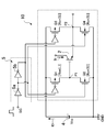
- FIG. 2 is a diagram illustrating a specific configuration example of a drive circuit illustrated in FIG. 1.
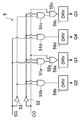
- FIG. 4 is a diagram showing another configuration example of a control circuit in the drive circuit shown in FIG. 2.
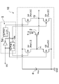
- FIG. 4 is a diagram showing still another configuration example of the control circuit in the drive circuit shown in FIG. 2.
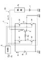
- FIG. 4 is a diagram illustrating another specific configuration example of the drive circuit illustrated in FIG. 1.
- the schematic block diagram which shows an example of the drive circuit of the conventional power element.
- the timing diagram which shows the on / off drive form of the power element by the drive circuit of the conventional power element.
- FIG. 1 is a schematic configuration diagram showing an outline of a power element drive circuit 10 according to an embodiment of the present invention. The same parts as those of the conventional drive circuit 1 shown in FIG. It is.
- the drive circuit 10 is connected in series and interposed between a power supply terminal (Vcc) and a ground terminal (GND), and the series connection point (node P1) is connected to the gate of the IGBT 2.
- First and second semiconductor switch elements Q1 and Q2 are provided. Further, the drive circuit 10 is connected in series and interposed between the power supply terminal (Vcc) and the ground terminal (GND), and the series connection point (node P2) is connected to the emitter of the IGBT 2.
- Third and fourth semiconductor switch elements Q3 and Q4 are provided.
- Each of the first to fourth semiconductor switch elements Q1, Q2, Q3, Q4 is made of, for example, a MOS-FET.
- the first semiconductor switch element Q1 among the first to fourth semiconductor switch elements Q1, Q2, Q3, Q4 is more on-resistance (conducting resistance) than the second to fourth semiconductor switch elements Q2, Q3, Q4.
- MOS-FET with a large Ron is used.
- the series circuit composed of the first and second semiconductor switch elements Q1 and Q2 and the series circuit composed of the third and fourth semiconductor switch elements Q3 and Q4 are arranged between the power supply terminal (Vcc) and the ground terminal (GND). Are provided in parallel to form a switch matrix circuit.
- This switch matrix circuit drives the IGBT 2 on / off by turning on / off the first to fourth semiconductor switch elements Q1, Q2, Q3, Q4 in relation to each other under the control of the control circuit 5. To do.
- the drive circuit 10 uses an element having a larger on-resistance than the second to fourth semiconductor switch elements Q2, Q3, Q4 as the first semiconductor switch element Q1 constituting the switch matrix circuit. It is characterized in that the gate resistance RG in the conventional drive circuit 1 shown in FIG. 6 is omitted. In other words, the configuration is such that the voltage of the node P1 in which the first and second semiconductor switch elements Q1 and Q2 are connected in series is directly applied to the gate of the IGBT 2 without going through the gate resistor RG.
- a MOS-FET having a large on-resistance Ron is used as the first semiconductor switch element Q1.
- MOS-FETs having a small on-resistance Ron are used as the second to fourth semiconductor switch elements Q2, Q3, and Q4. Therefore, here, the on-resistance of the first semiconductor switch element Q1 is indicated as Ron (L), and the on-resistances of the second to fourth semiconductor switch elements Q2, Q3, Q4 are indicated as Ron (S) [ ⁇ Ron (L)]. As shown.
- the first to fourth semiconductor switching elements Q1, Q2, Q3, and Q4 are basically composed of switching MOS-FETs having the same current capacity and the same breakdown voltage.
- the first semiconductor switch element Q1 having a particularly large on-resistance Ron is realized as a MOS-FET having a narrower channel width than the second to fourth semiconductor switch elements Q2, Q3, Q4, for example.
- the drive circuit 10 configured in this manner basically turns on the first and fourth semiconductor switch elements Q1 and Q4 in the normal operation in which the IGBT 2 is driven on and off, and the second and third semiconductor switch elements Q1 and Q4, respectively.
- the IGBT 2 is turned on by turning off the semiconductor switch elements Q2 and Q3, respectively.
- the first and fourth semiconductor switch elements Q1 and Q4 are turned off, and the second and third semiconductor switch elements Q2 and Q3 are turned on to turn off the IGBT 2.
- the control circuit 5 for turning on / off the first to fourth semiconductor switch elements Q1, Q2, Q3, and Q4 in association with each other is configured as shown in FIG. 2, for example.
- the control circuit 5 includes a first inverter circuit 5a that generates a drive signal that inverts the control signal SG to turn on and off the first and fourth semiconductor switch elements Q1 and Q4.
- the drive signal output from the first inverter circuit 5a is supplied with the power supply voltage Vcc of the power supply 4 or the ground potential (0 V) so as to turn the first and fourth semiconductor switch elements Q1 and Q4 on and off in opposition to each other. Takes two values.
- control circuit 5 includes a second inverter circuit 5b that generates a drive signal for inverting the output of the first inverter circuit 5a to turn on and off the second and third semiconductor switch elements Q2 and Q3.
- the drive signal output from the second inverter circuit 5b also takes the binary value of the power supply voltage Vcc of the power supply 4 or the ground potential (0V).
- the first and second semiconductor switch elements Q1 and Q2 connected in series receive the outputs of the first and second inverter circuits 5a and 5b and are mutually contradictory. Turn on and off.
- the third and fourth semiconductor switch elements Q3 and Q4 connected in series also receive the outputs of the first and second inverter circuits 5a and 5b and are turned on / off in a mutually contradictory manner.
- the third and fourth semiconductor switch elements Q3 and Q4 are turned on and off in a complementary manner to the on and off of the first and second semiconductor switch elements Q1 and Q.
- the on / off control of the first to fourth semiconductor switching elements Q1, Q2, Q3, and Q4 by the control circuit 5 controls the turn-on and turn-off of the IGBT 2, whereby the IGBT 2 is turned on / off. Driven off.
- the first semiconductor switch element Q1 is turned on and the second semiconductor switch element Q1 is turned on.
- the semiconductor switch element Q2 is turned off, the voltage V (P1) at the node P1 increases accordingly.
- the third semiconductor switch element Q3 is turned off and the fourth semiconductor switch element Q4 is turned on. Accordingly, the emitter voltage V (E) of the IGBT 2 is set to the ground potential (0V).
- the first semiconductor switch element Q1 when the first semiconductor switch element Q1 is turned off and the second semiconductor switch element Q2 is turned on, the voltage V (P1) of the node P1 is set to the ground potential (0V). At this time, the third semiconductor switch element Q3 is turned on and the fourth semiconductor switch element Q4 is turned off. Accordingly, the emitter voltage V (E) of the IGBT 2 is set to the power supply voltage Vcc. As a result, the gate-emitter voltage V (ge) of the IGBT 2 instantaneously becomes negative ( ⁇ Vcc), and the IGBT 2 is turned off.
- the charges accumulated in the gate capacitance of the IGBT 2 are discharged through the second semiconductor switch element Q2. Then, the voltage applied to the gate of the IGBT 2 returns to the ground potential (0V) as the gate capacitance of the IGBT 2 is discharged, and then the first semiconductor switch element Q1 in the off state and the second semiconductor switch element in the on state. A voltage (0 V) of the node P1 determined by Q2 is applied to the gate of the IGBT2. Therefore, IGBT2 maintains an OFF state.
- the gate capacitance of the IGBT 2 is charged via the first semiconductor switch element Q1 having a large on-resistance Ron. Can do. Further, when the IGBT 2 is turned off, the gate capacitance of the IGBT 2 can be instantaneously discharged through the second semiconductor switch element Q2 having a small on-resistance Ron. That is, the turn-on of the IGBT 2 can be delayed by the time required for charging the gate capacitance of the IGBT 2, and the gate capacitance of the IGBT 2 can be discharged instantly. As a result, since the gate resistance RG is not used, the switching loss when the IGBT 2 is turned off can be greatly reduced.
- the protection operation of the IGBT 2 by this short-circuit interruption is achieved by turning on the first and third semiconductor switch elements Q1 and Q3, respectively, and turning off the second and fourth semiconductor switch elements Q2 and Q4, respectively.
- a control circuit 5 is configured as shown in FIG. Accordingly, the on / off signals for the first to fourth semiconductor switch elements Q1, Q2, Q3, and Q4 may be switched.
- the control circuit 5 shown in FIG. 3 includes four AND circuits 51a, 51b, 51c, 51d whose gates are opened in response to the short circuit detection signal CO. These AND circuits 51a, 51b, 51c, 51d are connected via the inverter circuit 52 when the short circuit detection signal CO is not applied, in other words, when the short circuit detection signal CO is at a low level (L) and the IGBT 2 is normally operated. Each is established.
- the AND circuits 51a, 51b, 51c, and 51d supply the drive circuits 54a, 54b, 54c, and 54d with the control signal SC or a signal obtained by inverting the control signal SG via the inverter circuit 53, respectively.
- These drive circuits 53a, 53b, 53c, and 53d generate output voltages necessary to turn on / off the first to fourth semiconductor switch elements Q1, Q2, Q3, and Q4, respectively.
- the short circuit detection signal CO when the short circuit detection signal CO is applied, in other words, when the short circuit detection signal CO becomes the high level (H), the AND circuits 51a, 51b, 51c, 51d are closed. Then, the short circuit detection signal CO is supplied to the drive circuits 54a and 54c via the OR circuits 55a and 55c, respectively, and the short circuit detection signal CO inverted via the inverter circuit 52 is supplied to the drive circuit 54b via the AND circuits 51b and 51d. , 54d, respectively.
- the first and third semiconductor switch elements Q1, Q3 are forcibly turned on, and at the same time, the second and fourth semiconductor switch elements Q2, Q4 are forcibly turned off, respectively.
- the gate voltage V (G) of the IGBT 2 is set to the power supply voltage Vcc
- the emitter voltage V (E) of the IGBT 2 is also set to the power supply voltage Vcc.
- the gate-emitter voltage V (ge) of the IGBT 2 is forcibly set to 0 V
- the IGBT 2 is forcibly set to OFF.
- the first and third semiconductor switch elements Q1 and Q3 are turned on, and the voltages applied to the gate and emitter of the IGBT 2 are both set to the power supply voltage Vcc.
- the gate-emitter voltage V (ge) of the IGBT 2 becomes a negative voltage, and the IGBT 2 is turned off.
- the gate capacitance of the IGBT 2 is discharged through the first semiconductor switch element Q1. Since the gate-emitter voltage V (ge) of the IGBT 2 is maintained at 0V, the IGBT 2 maintains the off state.
- the second and fourth semiconductor switch elements Q2 and Q4 can be forcibly turned on instead of the above-described forced on of the first and third semiconductor switch elements Q1 and Q3 in the short circuit interruption. is there.
- the first and first semiconductor switch elements Q1, Q3 are forcibly turned off in conjunction with the second and fourth semiconductor switch elements Q2, Q4 being forcibly turned on.
- the gate voltage V (G) of the IGBT 2 becomes the ground potential.
- the emitter voltage V (E) of the IGBT 2 is also set to the ground potential (0V).
- the gate-emitter voltage V (ge) of the IGBT 2 becomes 0 V, and the IGBT 2 is forcibly turned off.
- the current Ic flowing through the load (RL) is cut off, and the IGBT 2 and the like are protected from the overcurrent accompanying the load short circuit.
- the control circuit 5 is, for example, as shown in FIG. What is necessary is just to comprise.
- the control circuit 5 shown in FIG. 4 gives the short circuit detection signal CO to the drive circuits 54a and 54c and is inverted through the inverter circuit 55 using the OR circuits 55b and 55d instead of the OR circuits 55a and 55c described above.
- the short circuit detection signal CO is provided to the drive circuits 54b and 54d, respectively.
- the second and fourth semiconductor switch elements Q2 and Q4 having a small on-resistance Ron are only turned on, the switching loss when the IGBT 2 is turned off can be further reduced. Can do.
- the power consumption in the drive circuit 10 can be reduced by the amount that is not accompanied by charge / discharge through the gate resistance RG of the gate capacitance of the IGBT 2.
- the manufacturing cost can be kept low.
- P-type MOS-FETs are used as the first and third semiconductor switch elements Q1, Q3, and N-type MOS-FETs are used as the second and fourth semiconductor switch elements Q2, Q4.
- An example was given.
- N-type MOS-FETs for the first to fourth semiconductor switch elements Q1, Q2, Q3, and Q4.
- a MOS-FET having a larger on-resistance Ron than the second to fourth semiconductor switch elements Q2, Q3, Q4 is used as the first semiconductor switch element Q1.
- the ON operation conditions of the first and third semiconductor switch elements Q1 and Q3 made of N-type MOS-FET are the first and second P-type MOS-FETs in the drive circuit 10 shown in FIG. 3 is different from the on-operation conditions of the semiconductor switch elements Q1 and Q3. That is, the first and third semiconductor switch elements Q1 and Q3 use the voltages of the nodes P1 and P2 that change as the first to fourth semiconductor switch elements Q1, Q2, Q3, and Q4 are turned on / off as the reference potential. As an on / off operation.
- the input and output of the inverter circuit 5c for inverting the control signal SG are connected to the first and third semiconductor switch elements Q1, Q3 via the level shift circuits 5d, 5e. What is necessary is just to comprise the control circuit 5 so that it may apply to each gate.
- the first and second semiconductor switches are also used in the drive circuit 10 in which the switch matrix circuit is configured by using N-type MOS-FETs as the first to fourth semiconductor switch elements Q1, Q2, Q3, and Q4. Since the voltage at the node P1, which is the series connection point of the elements Q1, Q2, is directly applied to the gate of the IGBT 2, the same effects as those of the above-described embodiment can be obtained.
- the present invention is not limited to the embodiment described above.
- P-type MOS-FETs as the first to fourth semiconductor switch elements Q1, Q2, Q3, and Q4, respectively.
- N-type MOS-FETs as the first and second semiconductor switch elements Q1 and Q2
- P-type MOS-FETs as the third and fourth semiconductor switch elements Q3 and Q4.
- the present invention can also be applied to the case where a power MOS-FET is driven as a power element.
- bipolar transistors may be used as the first to fourth semiconductor switching elements Q1, Q2, Q3, and Q4.
- control circuit 5 varies depending on the configuration of the switch matrix circuit and the on / off drive mode for the first to fourth semiconductor switch elements Q1, Q2, Q3, and Q4 constituting the switch matrix circuit. Is possible.
- present invention can be variously modified and implemented without departing from the scope of the invention.
Landscapes
- Engineering & Computer Science (AREA)
- Power Engineering (AREA)
- Power Conversion In General (AREA)
- Electronic Switches (AREA)
Abstract
IGBTのゲートに正バイアスまたは負バイアスを印加してIGBTをオン・オフ駆動する駆動回路において、IGBTのターン・オフ時におけるスイッチング損失を低減する。直列に接続されて電源端子と接地端子との間に介装されると共に、その直列接続点をIGBTのゲートに接続して設けた第1および第2の半導体スイッチ素子と、直列に接続されて電源端子と接地端子との間に介装されると共に、その直列接続点をIGBTのエミッタに接続して設けた第3および第4の半導体スイッチ素子とを備える。更に制御信号に応じて第1~第4の半導体スイッチ素子のそれぞれを互いに関連させてオン・オフさせてIGBTのオン・オフを制御する制御回路を備える。特に第1の半導体スイッチ素子として第2~第4の半導体スイッチ素子よりもオン抵抗の大きい素子を用いる。
Description
本発明は、IGBT等の電力素子をオン・オフ駆動する駆動回路に係り、特に電力素子のスイッチング損失を低減した簡易な構成の電力素子の駆動回路に関する。
図6は、IGBT等からなる電力素子2をオン・オフ駆動する従来の駆動回路1の一例を示す概略構成である。この駆動回路1は、IGBT(電力素子)2のゲートに印加する駆動信号をオン・オフし、該IGBT2のコレクタ・エミッタ間に流れる主電流を制御する役割を担う。このIGBT2のオン・オフにより、主電源3とIGBT2との間に接続された負荷(RL)に対する供給電流Icが制御される。
概略的には駆動回路1は、直列に接続されて電源4の電源端子(Vcc)と接地端子(GND)との間に介装された第1および第2の半導体スイッチ素子Q1,Q2と、直列に接続されて電源4の電源端子(Vcc)と接地端子(GND)との間に介装された第3および第4の半導体スイッチ素子Q3,Q4とを並列に備える。第1および第2の半導体スイッチ素子Q1,Q2は、その直列接続点(ノードP1)をゲート抵抗RGを介してIGBT2のゲートに接続したものである。また第3および第4の半導体スイッチ素子Q3,Q4は、その直列接続点(ノードP2)をIGBT2のエミッタに接続したものである。
これらの第1~第4の半導体スイッチ素子Q1,Q2,Q3,Q4のそれぞれは、例えばMOS-FETからなり、制御回路5の制御の下で互いに関連してオン・オフすることでIGBT2をオン・オフ駆動するスイッチ・マトリックス回路を構成する。尚、制御回路5は、外部から与えられる制御信号SGに応じて第1~第4の半導体スイッチ素子Q1,Q2,Q3,Q4のそれぞれを、互いに関連させてオン・オフさせてIGBT2のオン・オフを制御する役割を担う。
図7は、制御信号SGに応じた駆動回路1の各部の状態変化と、IGBT2の電圧変化を表す動作タイミングを示している。尚、図7においてV(P1)はノードP1の電圧変化、V(E)はIGBT2のエミッタ(ノードP2)の電圧変化、V(G)はIGBT2のゲートの電圧変化、そしてVgeはIGBT2のゲート・エミッタ間電圧の変化をそれぞれ示している。
図7に示すように駆動回路1は、制御信号SGに応じてIGBT2のゲート・エミッタ間電圧Vgeを正バイアスまたは負バイアスすることでIGBT2をオン・オフ駆動する。即ち、駆動回路1は、第1および第4の半導体スイッチ素子Q1,Q4をオンにすると共に、第2および第3の半導体スイッチ素子Q2,Q3をオフにすることで、ノードP1の電圧を電源4の電源電圧Vccに設定し、IGBT2のエミッタを接地する。そして駆動回路1は、ゲート抵抗RGを介してノードP1の電圧(電源電圧Vcc)をIGBT2のゲートに加えることでIGBT2をターン・オンさせる。
また駆動回路1は、第1および第4の半導体スイッチ素子Q1,Q4をオフにすると共に、第2および第3の半導体スイッチ素子Q2,Q3をオンにすることで、ノードP1を接地し、IGBT2のエミッタの電圧を電源4の電源電圧Vccに設定する、そして駆動回路1は、ゲート抵抗RGを介してIGBT2のゲートを接地することでIGBT2をターン・オフさせる。このように構成された駆動回路1については、例えば特許文献1に詳しく紹介される通りである。
ところで特許文献1に開示される駆動回路1は、電源4が出力する正の電源電圧Vccだけを用いてIGBT2を正バイアスまたは負バイアスしてIGBT2をオン・オフすることができ、負の電源を必要としない点で優れている。しかしながらこの従来の駆動回路1は、ノードP1の電圧V(P1)をゲート抵抗RGを介してIGBT2のゲートに印加し、これによってIGBT2のゲート容量を充放電する構成である。この為、IGBT2のターン・オン時、およびターン・オフ時におけるスイッチング損失が大きいと言う不具合がある。
この点、特許文献1には、第1~第4の半導体スイッチ素子Q1,Q2,Q3,Q4をオン・オフするタイミングにずれを持たせることで、IGBT2のターン・オン時、およびターン・オフ時におけるスイッチング損失を軽減することが開示されている。しかしながら第1~第4の半導体スイッチ素子Q1,Q2,Q3,Q4をそれぞれオン・オフするタイミングにずれを持たせる場合には、制御回路5の構成が複雑化すると言う新たな問題が発生する。更には駆動回路1を集積回路化する場合、第1~第4の半導体スイッチ素子Q1,Q2,Q3,Q4に比較して素子面積の大きいゲート抵抗RGが必要なので、駆動回路1の全体の回路面積が大型化すると言う不具合もある。
本発明はこのような事情を考慮してなされたもので、その目的は、上述したゲート抵抗を用いることなく、例えばIGBTからなる電力素子のターン・オフ時におけるスイッチング損失を低減することのできる、集積回路化に適した簡易な構成の電力素子の駆動回路を提供することにある。
本発明に係る電力素子の駆動回路は、制御電極に印加される駆動信号に応じて第1の主電極と第2の主電極との間に流れる主電流を制御する電力素子、例えばIGBTまたはN型のパワーMOS-FETをオン・オフ駆動するものである。
本発明に係る電力素子の駆動回路は、基本的には、
直列に接続されて電源端子と接地端子との間に介装されると共に、その直列接続点を前記電力素子の制御電極に接続して設けた第1および第2の半導体スイッチ素子と、
直列に接続されて前記電源端子と前記接地端子との間に介装されると共に、その直列接続点を前記電力素子の第2の主電極に接続して設けた第3および第4の半導体スイッチ素子と、
制御信号に応じて前記第1~第4の半導体スイッチ素子のそれぞれを互いに関連させてオン・オフさせて前記電力素子のオン・オフを制御する制御回路と
を備えて構成される。
直列に接続されて電源端子と接地端子との間に介装されると共に、その直列接続点を前記電力素子の制御電極に接続して設けた第1および第2の半導体スイッチ素子と、
直列に接続されて前記電源端子と前記接地端子との間に介装されると共に、その直列接続点を前記電力素子の第2の主電極に接続して設けた第3および第4の半導体スイッチ素子と、
制御信号に応じて前記第1~第4の半導体スイッチ素子のそれぞれを互いに関連させてオン・オフさせて前記電力素子のオン・オフを制御する制御回路と
を備えて構成される。
特に上述した目的を達成するべく本発明に係る電力素子の駆動回路は、前記電源端子側に接続された前記第1の半導体スイッチ素子として前記第2~第4の半導体スイッチ素子よりもオン抵抗の大きい素子を用いたことを特徴としている。
ちなみに前記電力素子は、例えば前記制御電極をゲート、前記第1の主電極をコレクタ、および前記第2の主電極をエミッタとするIGBTからなる。或いは前記電力素子は、前記制御電極をゲート、前記第1の主電極をソース、および前記第2の主電極をドレインとするN型のパワーMOS-FETからなる。そして前記第1~第4の半導体スイッチ素子のそれぞれは、前記制御回路から各ゲートに印加される電圧に応じてオン・オフするMOS-FETからなる。
好ましくは前記制御回路は、前記電力素子をオン・オフ駆動する通常動作時には、前記第1および第4の半導体スイッチ素子をそれぞれオンすると共に、前記第2および第3の半導体スイッチ素子をそれぞれオフさせて前記電力素子をターン・オンさせ、
更に前記第1および第4の半導体スイッチ素子をそれぞれオフすると共に、前記第2および第3の半導体スイッチ素子をそれぞれオンさせて前記電力素子をターン・オフさせるように構成される。
更に前記第1および第4の半導体スイッチ素子をそれぞれオフすると共に、前記第2および第3の半導体スイッチ素子をそれぞれオンさせて前記電力素子をターン・オフさせるように構成される。
また前記制御回路は、前記電力素子を強制的にオフさせる短絡遮断時には、前記第1および第3の半導体スイッチ素子をそれぞれオンさせると共に、前記第2および第4の半導体スイッチ素子をそれぞれオフさせるように構成される。或いは前記制御回路は、前記電力素子を強制的にオフさせる短絡遮断時には、前記第2および第4のスイッチ素子をそれぞれオンさせると共に、前記第1および第3の半導体スイッチ素子をそれぞれオフさせるように構成される。
本発明によれば、例えば同じ仕様のMOS-FETとして実現される第2~第4の半導体スイッチ素子に比較して、第1の半導体スイッチ素子としてチャネル幅の狭いMOS-FETを用いるだけで、該第1の半導体スイッチ素子のオン抵抗を前記第2~第4の半導体スイッチ素子の各オン抵抗よりも高くした電力素子の駆動回路を簡易に、しかも安価に実現することができる。
そして上記構成の電力素子の駆動回路によれば、前記電力素子(IGBT)をオンさせるべく前記第1の半導体スイッチ素子をオンすると共に前記第2の半導体スイッチ素子をオフすると、オン抵抗が大きい前記第1の半導体スイッチ素子を介して前記電力素子(IGBT)のゲート容量が充電される。また前記電力素子(IGBT)をオフさせるべく前記第1の半導体スイッチ素子をオフする共に前記第2の半導体スイッチ素子をオフすると、オン抵抗が小さい前記第2の半導体スイッチ素子を介して前記電力素子(IGBT)のゲート容量が放電される。
この結果、図6に例示した従来の駆動回路におけるゲート抵抗を用いることなく、前記電力素子(IGBT)のターン・オフ時における該電力素子でのスイッチング損失を低減することが可能となる。しかも前記第1の半導体スイッチ素子のオン抵抗を小さくしたことに伴う第1の半導体スイッチ素子の素子面積の縮小化と、ゲート抵抗を省いたこととが相まって、駆動回路全体をコンパクトに形成することが可能となる。更には回路構成自体を簡素化してその製造コストの低価格を図ることが可能となる等の実用上多大なる効果が祖せられる。
以下、図面を参照して本発明に係る電力素子の駆動回路10について説明する。
図1は、本発明の一実施形態に係る電力素子の駆動回路10の概要を示す概略構成図であり、図6に示した従来の駆動回路1と同一部分には同一符号を付して示してある。
この駆動回路10は、直列に接続されて電源端子(Vcc)と接地端子(GND)との間に介装されると共に、その直列接続点(ノードP1)をIGBT2のゲートに接続して設けた第1および第2の半導体スイッチ素子Q1,Q2を備える。更に駆動回路10は、直列に接続されて電源端子(Vcc)と接地端子(GND)との間に介装されると共に、その直列接続点(ノードP2)をIGBT2のエミッタに接続して設けた第3および第4の半導体スイッチ素子Q3,Q4を備える。
第1~第4の半導体スイッチ素子Q1,Q2,Q3,Q4のそれぞれは、例えばMOS-FETからなる。特に第1~第4の半導体スイッチ素子Q1,Q2,Q3,Q4のうち第1の半導体スイッチ素子Q1としては、第2~第4の半導体スイッチ素子Q2,Q3,Q4よりもオン抵抗(導通抵抗)Ronの大きいMOS-FETが用いられている。
第1および第2の半導体スイッチ素子Q1,Q2からなる直列回路と、第3および第4の半導体スイッチ素子Q3,Q4からなる直列回路は、電源端子(Vcc)と接地端子(GND)との間に並列に設けられてスイッチ・マトリックス回路を構成する。このスイッチ・マトリックス回路は、制御回路5の制御の下で第1~第4の半導体スイッチ素子Q1,Q2,Q3,Q4のそれぞれを互いに関連してオン・オフすることでIGBT2をオン・オフ駆動する。
即ち、本発明に係る駆動回路10は、スイッチ・マトリックス回路を構成する第1の半導体スイッチ素子Q1として第2~第4の半導体スイッチ素子Q2,Q3,Q4よりもオン抵抗の大きい素子を用い、図6に示した従来の駆動回路1におけるゲート抵抗RGを省いたことを特徴としている。換言すれば第1および第2の半導体スイッチ素子Q1,Q2を直列に接続したノードP1の電圧を、ゲート抵抗RGを介することなくIGBT2のゲートに直接印加するように構成したことを特徴としている。
具体的には、例えば図2に示すように第1の半導体スイッチ素子Q1としては、オン抵抗Ronの大きいMOS-FETが用いられる。また第2~第4の半導体スイッチ素子Q2,Q3,Q4としては、オン抵抗Ronの小さいMOS-FETがそれぞれ用いられる。従ってここでは第1の半導体スイッチ素子Q1のオン抵抗をRon(L)として示し、第2~第4の半導体スイッチ素子Q2,Q3,Q4のオン抵抗をRon(S)[<Ron(L)]として示す。
ちなみに第1~第4の半導体スイッチ素子Q1,Q2,Q3,Q4は、基本的には互いに同じスイッチ特性を有する同一の電流容量で、且つ同一の耐圧を有するスイッチング用のMOS-FETからなる。しかしここでは、特にオン抵抗Ronの大きい第1の半導体スイッチ素子Q1は、例えば第2~第4の半導体スイッチ素子Q2,Q3,Q4に比較してチャネル幅の狭いMOS-FETとして実現される。
このように構成された駆動回路10は、基本的にはIGBT2をオン・オフ駆動する通常動作時には、第1および第4の半導体スイッチ素子Q1,Q4をそれぞれオンすると共に、第2および第3の半導体スイッチ素子Q2,Q3をそれぞれオフさせることでIGBT2をターン・オンさせる。また第1および第4の半導体スイッチ素子Q1,Q4をそれぞれオフすると共に、第2および第3の半導体スイッチ素子Q2,Q3をそれぞれオンさせることでIGBT2をターン・オフさせる。
このようにして第1~第4の半導体スイッチ素子Q1,Q2,Q3,Q4を互いに関連させてオン・オフする制御回路5は、例えば図2に示すように構成される。具体的には制御回路5は、制御信号SGを反転させて第1および第4の半導体スイッチ素子Q1,Q4をオン・オフする駆動信号を生成する第1のインバータ回路5aを備える。この第1のインバータ回路5aが出力する駆動信号は、第1および第4の半導体スイッチ素子Q1,Q4を互いに相反させてオン・オフするべく、電源4の電源電圧Vccまたは接地電位(0V)の2値をとる。
更に制御回路5は、第1のインバータ回路5aの出力を反転して第2および第3の半導体スイッチ素子Q2,Q3をオン・オフする駆動信号を生成する第2のインバータ回路5bを備える。この第2のインバータ回路5bが出力する駆動信号もまた、電源4の電源電圧Vccまたは接地電位(0V)の2値をとる。
このように構成された制御回路5によれば、直列に接続された第1および第2の半導体スイッチ素子Q1,Q2は、第1および第2のインバータ回路5a,5bの出力を受けて互いに相反してオン・オフする。また直列に接続された第3および第4の半導体スイッチ素子Q3,Q4もまた、第1および第2のインバータ回路5a,5bの出力を受けて互いに相反してオン・オフする。特に第3および第4の半導体スイッチ素子Q3,Q4は、第1および第2の半導体スイッチ素子Q1,Qのオン・オフとは相補的にオン・オフする。そして制御回路5による第1~第4の半導体スイッチ素子Q1,Q2,Q3,Q4の互いに関連したオン・オフ制御により、IGBT2のターン・オンおよびターン・オフが制御され、これによってIGBT2がオン・オフ駆動される。
上述した如く制御回路5の制御の下でオン・オフされる第1~第4の半導体スイッチ素子Q1,Q2,Q3,Q4によれば、第1の半導体スイッチ素子Q1がオンすると共に第2の半導体スイッチ素子Q2がオフすると、これに伴ってノードP1の電圧V(P1)が高くなる。このとき第3の半導体スイッチ素子Q3がオフし、また第4の半導体スイッチ素子Q4がオンするので、これに伴ってIGBT2のエミッタの電圧V(E)が接地電位(0V)に設定される。
するとIGBT2のゲートには第1の半導体スイッチ素子Q1のオン抵抗Ron(L)を介して電流が流れ込み、IGBT2のゲート容量が充電される。そしてIGBT2のゲート容量の充電に伴って該IGBT2のゲートに加わる電圧が高くなり、ゲート電圧がIGBT2の閾値電圧を超えると、これによってIGBT2がターン・オンする。
一方、第1の半導体スイッチ素子Q1がオフすると共に第2の半導体スイッチ素子Q2がオンすると、ノードP1の電圧V(P1)が接地電位(0V)に設定される。またこの時、第3の半導体スイッチ素子Q3がオンし、第4の半導体スイッチ素子Q4がオフするので、これに伴ってIGBT2のエミッタの電圧V(E)が電源電圧Vccに設定される。この結果、IGBT2のゲート・エミッタ間電圧V(ge)が瞬時的に負(-Vcc)となり、IGBT2がターン・オフする。
またこのとき、IGBT2のゲート容量に蓄積されていた電荷は、第2の半導体スイッチ素子Q2を介して放電される。そしてIGBT2のゲート容量の放電に伴って該IGBT2のゲートに加わる電圧が接地電位(0V)に戻り、その後、オフ状態にある第1の半導体スイッチ素子Q1とオン状態にある第2の半導体スイッチ素子Q2とによって定まるノードP1の電圧(0V)がIGBT2のゲートに加えられる。従ってIGBT2はオフ状態を維持する。
従って上述した如く構成された駆動回路10によれば、通常動作時においてIGBT2をターン・オンさせる際にはオン抵抗Ronの大きい第1の半導体スイッチ素子Q1を介してIGBT2のゲート容量を充電することができる。またIGBT2をターン・オフさせる際にはオン抵抗Ronの小さい第2の半導体スイッチ素子Q2を介してIGBT2のゲート容量を瞬時に放電させることができる。即ち、IGBT2のゲート容量の充電に要する時間でIGBT2のターン・オンを遅らせることができ、またIGBT2のゲート容量を瞬時に放電させることができる。この結果、ゲート抵抗RGを用いない分、IGBT2のターン・オフ時におけるスイッチング損失を大幅に低減することができる。
ところでIGBT2を介して電流Icが供給される負荷側において短絡が検出された場合には、IGBT2を強制的にオフさせて過大な短絡電流からIGBT2や負荷(RL)を保護し、更には駆動回路1,10を保護することが行われる。
この短絡遮断によるIGBT2の保護動作は、例えば第1および第3の半導体スイッチ素子Q1,Q3をそれぞれオンすると共に、第2および第4の半導体スイッチ素子Q2,Q4をそれぞれオフにすることによって達せられる。具体的には短絡遮断検出時に第1および第3の半導体スイッチ素子Q1,Q3をそれぞれ強制的にオンする場合には、例えば図3に示すように制御回路5を構成し、短絡検出信号COに応じて第1~第4の半導体スイッチ素子Q1,Q2,Q3,Q4に対するオン・オフ信号を切り替えるようにすれば良い。
この図3に示す制御回路5は、短絡検出信号COに応じてゲートが開成される4つのアンド回路51a,51b,51c,51dを備える。これらアンド回路51a,51b,51c,51dは、短絡検出信号COが印加されないとき、換言すれば短絡検出信号COがローレベル(L)であり、IGBT2を通常動作させるとき、インバータ回路52を介してそれぞれ開成される。そしてアンド回路51a,51b,51c,51dは、制御信号SCまたはインバータ回路53を介して制御信号SGを反転した信号を、ドライブ回路54a,54b,54c,54dにそれぞれ与える。尚、これらのドライブ回路53a,53b,53c,53dは、第1~第4の半導体スイッチ素子Q1,Q2,Q3,Q4をそれぞれオン・オフするに必要な出力電圧を生成するものである。
これに対して短絡検出信号COが印加されたとき、換言すれば短絡検出信号COがハイレベル(H)になった時、アンド回路51a,51b,51c,51dがそれぞれ閉じられる。そして短絡検出信号COがオア回路55a,55cを介してドライブ回路54a,54cにそれぞれ与られると共に、インバータ回路52を介して反転された短絡検出信号COがアンド回路51b,51dを介してドライブ回路54b,54dにそれぞれ与られる。
従って短絡検出信号COが与えられたときには第1および第3の半導体スイッチ素子Q1,Q3がそれぞれ強制的にオンされ、同時に第2および第4の半導体スイッチ素子Q2,Q4がそれぞれ強制的にオフされる。この結果、IGBT2のゲート電圧V(G)が電源電圧Vccに設定されると共に、該IGBT2のエミッタ電圧V(E)もまた電源電圧Vccに設定される。するとIGBT2のゲート・エミッタ間電圧V(ge)が強制的に0Vに設定されて該IGBT2が強制的にオフに設定される。そしてIGBT2の強制的なオフに伴って負荷(RL)に流れる電流Icが遮断され、負荷短絡に伴う過電流からIGBT2等が保護される。
このように構成された駆動回路10によれば、第1および第3の半導体スイッチ素子Q1,Q3をそれぞれオンし、IGBT2のゲートおよびエミッタに加わる電圧を共に電源電圧Vccに設定するだけである。この際、IGBT2のゲート容量の充電に要する時間、IGBT2のゲート・エミッタ間電圧V(ge)が負電圧となり、IGBT2がターン・オフする。そしてIGBT2のターン・オフに伴ってIGBT2のゲート容量が第1の半導体スイッチ素子Q1を介して放電される。そしてIGBT2のゲート・エミッタ間電圧V(ge)が0Vに保たれるので、IGBT2はオフ状態を維持する。
従って短絡遮断検出時に第1および第3の半導体スイッチ素子Q1,Q3をそれぞれ強制的にオンする場合であっても、従来のようにゲート抵抗RGを介するIGBT2のゲート容量の充放電がないので、IGBT2のターン・オフ時におけるスイッチング損失を低減することができる。従って駆動回路10での消費電力を小さくすることができる。
尚、短絡遮断における上述した第1および第3の半導体スイッチ素子Q1,Q3の強制的なオンに代えて、第2および第4の半導体スイッチ素子Q2,Q4を強制的にオンすることも可能である。この場合、第2および第4の半導体スイッチ素子Q2,Q4の強制的にオンに連動させて第1および第1の半導体スイッチ素子Q1,Q3を強制的にオフすることは言うまでもない。
このようにして第1および第3の半導体スイッチ素子Q1,Q3をオフにし、同時に第2および第4の半導体スイッチ素子Q2,Q4をオンにすれば、IGBT2のゲート電圧V(G)が接地電位(0V)に設定されると共に、該IGBT2のエミッタ電圧V(E)もまた接地電位(0V)に設定される。この結果、IGBT2のゲート・エミッタ間電圧V(ge)が0Vとなり、該IGBT2が強制的にオフとなる。そしてIGBT2の強制的なオフに伴って負荷(RL)に流れる電流Icが遮断され、負荷短絡に伴う過電流からIGBT2等が保護される。
尚、短絡検出信号COが与えられたときに上述した如く第2および第4の半導体スイッチ素子Q2,Q4をそれぞれ強制的にオンする場合には、制御回路5を、例えば図4に示すように構成すれば良い。図4に示す制御回路5は、短絡検出信号COをドライブ回路54a,54cに与えると共に、前述したオア回路55a,55cに代わるオア回路55b,55dを用いて、インバータ回路55を介して反転された短絡検出信号COをドライブ回路54b,54dにそれぞれ与えるように構成される。
このように構成された駆動回路10によれば、オン抵抗Ronが小さい第2および第4の半導体スイッチ素子Q2,Q4をオンするだけなので、IGBT2のターン・オフ時におけるスイッチング損失を更に小さくすることができる。そしてIGBT2のゲート容量のゲート抵抗RGを介する充放電を伴うことがない分、駆動回路10での消費電力を小さくすることができる。
しかも従来の制御回路1において用いられていたゲート抵抗RGを省いた上で第1の半導体スイッチ素子Q1の小型化を図ることができる。従って駆動回路10を集積回路化する上でチップ面積を小さくすることができる。また半導体チップ上にMOS-FET等と並べてゲート抵抗RGを形成する必要がないので、その製造コストを低く抑えることが可能となる等の効果が奏せられる。
ところで上述した説明においては、第1および第3の半導体スイッチ素子Q1,Q3としてP型のMOS-FETを用い、第2および第4の半導体スイッチ素子Q2,Q4としてN型のMOS-FETを用いた例について示した。しかし図5に例示するように、第1~第4の半導体スイッチ素子Q1,Q2,Q3,Q4のそれぞれにN型のMOS-FETを用いてスイッチ・マトリックス回路を構成することも可能である。この場合においても第1の半導体スイッチ素子Q1として、第2~第4の半導体スイッチ素子Q2,Q3,Q4よりもオン抵抗Ronの大きいMOS-FETを用いることは言うまでもない。
この場合、N型のMOS-FETからなる第1および第3の半導体スイッチ素子Q1,Q3のオン動作条件が、図2に示した駆動回路10におけるP型のMOS-FETからなる第1および第3の半導体スイッチ素子Q1,Q3のオン動作条件とは異なる。即ち、第1および第3の半導体スイッチ素子Q1,Q3は、第1~第4の半導体スイッチ素子Q1,Q2,Q3,Q4のオン・オフに伴って変化するノードP1,P2の電圧を基準電位としてオン・オフ動作する。
従ってこの場合には、図5に示すように制御信号SGを反転するインバータ回路5cの入力と出力とをレベルシフト回路5d,5eを介して第1および第3の半導体スイッチ素子Q1,Q3の各ゲートにそれぞれ印加するように制御回路5を構成すれば良い。このように第1~第4の半導体スイッチ素子Q1,Q2,Q3,Q4としてN型のMOS-FETを用いてスイッチ・マトリックス回路を構成した駆動回路10においても、第1および第2の半導体スイッチ素子Q1,Q2の直列接続点であるノードP1の電圧をIGBT2のゲートに直接印加するので、前述した実施形態と同様な効果が奏せられる。
尚、本発明は上述した実施形態に限定されるものではない。例えば特に図示しないが第1~第4の半導体スイッチ素子Q1,Q2,Q3,Q4としてP型のMOS-FETをそれぞれ用いることも勿論可能である。また第1および第2の半導体スイッチ素子Q1,Q2としてN型のMOS-FETを用い、第3および第4の半導体スイッチ素子Q3,Q4としてP型のMOS-FETを用いることも勿論可能である。
また第1の半導体スイッチ素子Q1のオン抵抗Ronについては、IGBT2を確実にターン・オンさせるに必要な時間に亘ってIGBT2のゲート容量を充電し得る値として設定すれば十分である。また前述したように電力素子としてパワーMOS-FETを駆動する場合にも本発明を適用可能なことは勿論である。更には第1~第4の半導体スイッチ素子Q1,Q2,Q3,Q4としてバイポーラ・トランジスタを用いても良いことは言うまでもない。
また制御回路5の構成についてスイッチ・マトリックス回路の構成や、スイッチ・マトリックス回路を構成する第1~第4の半導体スイッチ素子Q1,Q2,Q3,Q4に対するオン・オフ駆動形態等に応じて種々変化可能である。その他、本発明はその要旨を逸脱しない範囲で種々変形して実施することができる。
1,10 駆動回路
2 電力素子(IGBT)
3 主電源
4 電源(Vcc)
5 制御回路(CONT)
Q1 第1のスイッチ素子(MOS-FET)
Q2 第2のスイッチ素子(MOS-FET)
Q3 第3のスイッチ素子(MOS-FET)
Q3 第4のスイッチ素子(MOS-FET)
RG ゲート抵抗
2 電力素子(IGBT)
3 主電源
4 電源(Vcc)
5 制御回路(CONT)
Q1 第1のスイッチ素子(MOS-FET)
Q2 第2のスイッチ素子(MOS-FET)
Q3 第3のスイッチ素子(MOS-FET)
Q3 第4のスイッチ素子(MOS-FET)
RG ゲート抵抗
Claims (6)
- 制御電極に印加される駆動信号に応じて第1の主電極と第2の主電極との間に流れる主電流を制御する電力素子をオン・オフ駆動する駆動回路であって、
直列に接続されて電源端子と接地端子との間に介装されると共に、その直列接続点を前記電力素子の制御電極に接続して設けた第1および第2の半導体スイッチ素子と、
直列に接続されて前記電源端子と前記接地端子との間に介装されると共に、その直列接続点を前記電力素子の第2の主電極に接続して設けた第3および第4の半導体スイッチ素子と、
制御信号に応じて前記第1~第4の半導体スイッチ素子のそれぞれを互いに関連させてオン・オフさせて前記電力素子のオン・オフを制御する制御回路と
を具備し、
前記電源端子側に接続された前記第1の半導体スイッチ素子として前記第2~第4の半導体スイッチ素子よりもオン抵抗の大きい素子を用いることを特徴とする電力素子の駆動回路。 - 前記電力素子は、前記制御電極をゲート、前記第1の主電極をコレクタ、および前記第2の主電極をエミッタとするIGBTであって、
前記第1~第4の半導体スイッチ素子のそれぞれは、前記制御回路から各ゲートに印加される電圧に応じてオン・オフするMOS-FETである請求項1に記載の電力素子の駆動回路。 - 前記電力素子は、前記制御電極をゲート、前記第1の主電極をソース、および前記第2の主電極をドレインとするN型のパワーMOS-FETであって、
前記第1~第4の半導体スイッチ素子のそれぞれは、前記制御回路から各ゲートに印加される電圧に応じてオン・オフするMOS-FETである請求項1に記載の電力素子の駆動回路。 - 前記制御回路は、前記電力素子をオン・オフ駆動する通常動作時には、前記第1および第4の半導体スイッチ素子をそれぞれオンすると共に、前記第2および第3の半導体スイッチ素子をそれぞれオフさせて前記電力素子をターン・オンさせ、
前記第1および第4の半導体スイッチ素子をそれぞれオフすると共に、前記第2および第3の半導体スイッチ素子をそれぞれオンさせて前記電力素子をターン・オフさせるものである請求項1に記載の電力素子の駆動回路。 - 前記制御回路は、前記電力素子を強制的にオフさせる短絡遮断時には、前記第1および第3の半導体スイッチ素子をそれぞれオンさせると共に、前記第2および第4の半導体スイッチ素子をそれぞれオフさせるものである請求項1に記載の電力素子の駆動回路。
- 前記制御回路は、前記電力素子を強制的にオフさせる短絡遮断時には、前記第2および第4のスイッチ素子をそれぞれオンさせると共に、前記第1および第3の半導体スイッチ素子をそれぞれオフさせるものである請求項1に記載の電力素子の駆動回路。
Priority Applications (3)
| Application Number | Priority Date | Filing Date | Title |
|---|---|---|---|
| JP2018538317A JP6760383B2 (ja) | 2016-09-09 | 2017-08-08 | 電力素子の駆動回路 |
| CN201780014834.XA CN108702150B (zh) | 2016-09-09 | 2017-08-08 | 功率元件的驱动电路 |
| US16/119,290 US10911030B2 (en) | 2016-09-09 | 2018-08-31 | Drive circuit for power element |
Applications Claiming Priority (2)
| Application Number | Priority Date | Filing Date | Title |
|---|---|---|---|
| JP2016176892 | 2016-09-09 | ||
| JP2016-176892 | 2016-09-09 |
Related Child Applications (1)
| Application Number | Title | Priority Date | Filing Date |
|---|---|---|---|
| US16/119,290 Continuation-In-Part US10911030B2 (en) | 2016-09-09 | 2018-08-31 | Drive circuit for power element |
Publications (1)
| Publication Number | Publication Date |
|---|---|
| WO2018047561A1 true WO2018047561A1 (ja) | 2018-03-15 |
Family
ID=61562041
Family Applications (1)
| Application Number | Title | Priority Date | Filing Date |
|---|---|---|---|
| PCT/JP2017/028656 Ceased WO2018047561A1 (ja) | 2016-09-09 | 2017-08-08 | 電力素子の駆動回路 |
Country Status (4)
| Country | Link |
|---|---|
| US (1) | US10911030B2 (ja) |
| JP (1) | JP6760383B2 (ja) |
| CN (1) | CN108702150B (ja) |
| WO (1) | WO2018047561A1 (ja) |
Cited By (2)
| Publication number | Priority date | Publication date | Assignee | Title |
|---|---|---|---|---|
| JP2019198187A (ja) * | 2018-05-10 | 2019-11-14 | 富士電機株式会社 | ゲート駆動装置およびスイッチ装置 |
| JP2020039204A (ja) * | 2018-09-03 | 2020-03-12 | 株式会社デンソー | 駆動対象スイッチの駆動回路 |
Citations (4)
| Publication number | Priority date | Publication date | Assignee | Title |
|---|---|---|---|---|
| JPH1197994A (ja) * | 1997-09-19 | 1999-04-09 | Fuji Electric Co Ltd | Mosゲート形素子の駆動回路 |
| JP5011585B2 (ja) * | 2007-07-03 | 2012-08-29 | 三菱電機株式会社 | 電力素子の駆動回路 |
| US8258823B2 (en) * | 2009-05-11 | 2012-09-04 | Sma Solar Technology Ag | Method of and driver circuit for operating a semiconductor power switch |
| JP2015032984A (ja) * | 2013-08-02 | 2015-02-16 | 株式会社 日立パワーデバイス | 半導体素子の駆動装置およびそれを用いた電力変換装置 |
Family Cites Families (14)
| Publication number | Priority date | Publication date | Assignee | Title |
|---|---|---|---|---|
| JPH088703A (ja) * | 1994-06-21 | 1996-01-12 | Sekisui Chem Co Ltd | Fetの駆動回路 |
| US7274242B2 (en) * | 2004-11-02 | 2007-09-25 | Rambus Inc. | Pass transistors with minimized capacitive loading |
| WO2006070524A1 (ja) * | 2004-12-28 | 2006-07-06 | Rohm Co., Ltd | 電源回路、チャージポンプ回路、及び、これを備えた携帯機器 |
| JP4573843B2 (ja) * | 2007-01-18 | 2010-11-04 | 株式会社豊田中央研究所 | 電力用半導体素子の駆動回路 |
| US7960997B2 (en) * | 2007-08-08 | 2011-06-14 | Advanced Analogic Technologies, Inc. | Cascode current sensor for discrete power semiconductor devices |
| JP5401774B2 (ja) * | 2007-08-27 | 2014-01-29 | 富士電機株式会社 | 半導体素子のゲート駆動回路 |
| US9806593B2 (en) * | 2008-08-21 | 2017-10-31 | Mitsubishi Electric Corporation | Drive circuit of power semiconductor device |
| JP5678498B2 (ja) * | 2010-07-15 | 2015-03-04 | 富士電機株式会社 | 電力用半導体素子のゲート駆動回路 |
| JP5733330B2 (ja) * | 2013-03-22 | 2015-06-10 | 株式会社デンソー | 駆動回路 |
| US9035687B2 (en) * | 2013-10-09 | 2015-05-19 | Infineon Technologies Ag | Gate clamping |
| KR102112299B1 (ko) * | 2014-01-10 | 2020-05-18 | 삼성전자주식회사 | 파워 스위치 소자의 구동 방법 및 구동 회로 |
| US9621162B2 (en) * | 2014-05-27 | 2017-04-11 | Nxp Usa, Inc. | High side driver component and method therefor |
| KR101639488B1 (ko) * | 2014-12-10 | 2016-07-13 | 현대모비스 주식회사 | 암 쇼트 방지를 위한 게이트 구동 회로 및 방법 |
| DE102015201045B4 (de) * | 2015-01-22 | 2019-09-26 | Infineon Technologies Austria Ag | Mit einer hohen Gate-Spannung betreibbarer Hochspannungstransistor, Verfahren zum Steuern desselben und Schaltungsanordnung |
-
2017
- 2017-08-08 CN CN201780014834.XA patent/CN108702150B/zh active Active
- 2017-08-08 JP JP2018538317A patent/JP6760383B2/ja active Active
- 2017-08-08 WO PCT/JP2017/028656 patent/WO2018047561A1/ja not_active Ceased
-
2018
- 2018-08-31 US US16/119,290 patent/US10911030B2/en active Active
Patent Citations (4)
| Publication number | Priority date | Publication date | Assignee | Title |
|---|---|---|---|---|
| JPH1197994A (ja) * | 1997-09-19 | 1999-04-09 | Fuji Electric Co Ltd | Mosゲート形素子の駆動回路 |
| JP5011585B2 (ja) * | 2007-07-03 | 2012-08-29 | 三菱電機株式会社 | 電力素子の駆動回路 |
| US8258823B2 (en) * | 2009-05-11 | 2012-09-04 | Sma Solar Technology Ag | Method of and driver circuit for operating a semiconductor power switch |
| JP2015032984A (ja) * | 2013-08-02 | 2015-02-16 | 株式会社 日立パワーデバイス | 半導体素子の駆動装置およびそれを用いた電力変換装置 |
Cited By (4)
| Publication number | Priority date | Publication date | Assignee | Title |
|---|---|---|---|---|
| JP2019198187A (ja) * | 2018-05-10 | 2019-11-14 | 富士電機株式会社 | ゲート駆動装置およびスイッチ装置 |
| JP7091819B2 (ja) | 2018-05-10 | 2022-06-28 | 富士電機株式会社 | ゲート駆動装置およびスイッチ装置 |
| JP2020039204A (ja) * | 2018-09-03 | 2020-03-12 | 株式会社デンソー | 駆動対象スイッチの駆動回路 |
| JP7099199B2 (ja) | 2018-09-03 | 2022-07-12 | 株式会社デンソー | 駆動対象スイッチの駆動回路 |
Also Published As
| Publication number | Publication date |
|---|---|
| US10911030B2 (en) | 2021-02-02 |
| JP6760383B2 (ja) | 2020-09-23 |
| CN108702150B (zh) | 2021-12-21 |
| JPWO2018047561A1 (ja) | 2018-12-27 |
| CN108702150A (zh) | 2018-10-23 |
| US20180375499A1 (en) | 2018-12-27 |
Similar Documents
| Publication | Publication Date | Title |
|---|---|---|
| JP5011585B2 (ja) | 電力素子の駆動回路 | |
| JP5354417B2 (ja) | レベルシフト回路 | |
| JP4901445B2 (ja) | 駆動回路及びこれを用いた半導体装置 | |
| JP2019519150A (ja) | エンハンスメントモードfetドライバic | |
| JP6569821B2 (ja) | 電力素子の駆動回路 | |
| CN106357251A (zh) | 半导体开关装置 | |
| JP3702159B2 (ja) | 半導体集積回路装置 | |
| US10063226B2 (en) | Level shift circuit | |
| JP2002290221A (ja) | 半導体出力回路の消費電力低減回路 | |
| JP4160127B2 (ja) | スルーイング制御手段を有する出力段 | |
| US5864245A (en) | Output circuit with overvoltage protection | |
| JP2017079534A (ja) | ゲート制御回路 | |
| JP5383353B2 (ja) | 異常検出時急速放電回路 | |
| JP6760383B2 (ja) | 電力素子の駆動回路 | |
| JP6569820B2 (ja) | 電力素子の駆動回路 | |
| JP2000307406A (ja) | 負荷駆動回路 | |
| US10425078B2 (en) | High-side power switch control circuit | |
| KR100361901B1 (ko) | 출력드라이버의스위칭으로인한방해를감소시키는회로 | |
| JPH02197213A (ja) | 過大電流防止回路を備えた負荷駆動装置 | |
| JP2008283277A (ja) | 半導体スイッチ回路 | |
| JPH0477015A (ja) | 光結合型リレー回路 | |
| JPS62224117A (ja) | 信号出力回路 | |
| JP2014168131A (ja) | Cmosインバータ回路 | |
| JP2020061675A (ja) | スイッチング回路 | |
| JP2002300018A (ja) | レベルシフト回路 |
Legal Events
| Date | Code | Title | Description |
|---|---|---|---|
| WWE | Wipo information: entry into national phase |
Ref document number: 2018538317 Country of ref document: JP |
|
| 121 | Ep: the epo has been informed by wipo that ep was designated in this application |
Ref document number: 17848505 Country of ref document: EP Kind code of ref document: A1 |
|
| NENP | Non-entry into the national phase |
Ref country code: DE |
|
| 122 | Ep: pct application non-entry in european phase |
Ref document number: 17848505 Country of ref document: EP Kind code of ref document: A1 |