WO2018033964A1 - 系統連系インバータ装置及びその運転方法 - Google Patents
系統連系インバータ装置及びその運転方法 Download PDFInfo
- Publication number
- WO2018033964A1 WO2018033964A1 PCT/JP2016/073928 JP2016073928W WO2018033964A1 WO 2018033964 A1 WO2018033964 A1 WO 2018033964A1 JP 2016073928 W JP2016073928 W JP 2016073928W WO 2018033964 A1 WO2018033964 A1 WO 2018033964A1
- Authority
- WO
- WIPO (PCT)
- Prior art keywords
- power
- modulation method
- voltage
- voltage drop
- switching elements
- Prior art date
- Legal status (The legal status is an assumption and is not a legal conclusion. Google has not performed a legal analysis and makes no representation as to the accuracy of the status listed.)
- Ceased
Links
Images




Classifications
-
- H—ELECTRICITY
- H02—GENERATION; CONVERSION OR DISTRIBUTION OF ELECTRIC POWER
- H02M—APPARATUS FOR CONVERSION BETWEEN AC AND AC, BETWEEN AC AND DC, OR BETWEEN DC AND DC, AND FOR USE WITH MAINS OR SIMILAR POWER SUPPLY SYSTEMS; CONVERSION OF DC OR AC INPUT POWER INTO SURGE OUTPUT POWER; CONTROL OR REGULATION THEREOF
- H02M7/00—Conversion of AC power input into DC power output; Conversion of DC power input into AC power output
- H02M7/42—Conversion of DC power input into AC power output without possibility of reversal
- H02M7/44—Conversion of DC power input into AC power output without possibility of reversal by static converters
- H02M7/48—Conversion of DC power input into AC power output without possibility of reversal by static converters using discharge tubes with control electrode or semiconductor devices with control electrode
- H02M7/53—Conversion of DC power input into AC power output without possibility of reversal by static converters using discharge tubes with control electrode or semiconductor devices with control electrode using devices of a triode or transistor type requiring continuous application of a control signal
- H02M7/537—Conversion of DC power input into AC power output without possibility of reversal by static converters using discharge tubes with control electrode or semiconductor devices with control electrode using devices of a triode or transistor type requiring continuous application of a control signal using semiconductor devices only, e.g. single switched pulse inverters
- H02M7/5387—Conversion of DC power input into AC power output without possibility of reversal by static converters using discharge tubes with control electrode or semiconductor devices with control electrode using devices of a triode or transistor type requiring continuous application of a control signal using semiconductor devices only, e.g. single switched pulse inverters in a bridge configuration
- H02M7/53871—Conversion of DC power input into AC power output without possibility of reversal by static converters using discharge tubes with control electrode or semiconductor devices with control electrode using devices of a triode or transistor type requiring continuous application of a control signal using semiconductor devices only, e.g. single switched pulse inverters in a bridge configuration with automatic control of output voltage or current
-
- H—ELECTRICITY
- H02—GENERATION; CONVERSION OR DISTRIBUTION OF ELECTRIC POWER
- H02M—APPARATUS FOR CONVERSION BETWEEN AC AND AC, BETWEEN AC AND DC, OR BETWEEN DC AND DC, AND FOR USE WITH MAINS OR SIMILAR POWER SUPPLY SYSTEMS; CONVERSION OF DC OR AC INPUT POWER INTO SURGE OUTPUT POWER; CONTROL OR REGULATION THEREOF
- H02M1/00—Details of apparatus for conversion
- H02M1/08—Circuits specially adapted for the generation of control voltages for semiconductor devices incorporated in static converters
-
- H—ELECTRICITY
- H02—GENERATION; CONVERSION OR DISTRIBUTION OF ELECTRIC POWER
- H02M—APPARATUS FOR CONVERSION BETWEEN AC AND AC, BETWEEN AC AND DC, OR BETWEEN DC AND DC, AND FOR USE WITH MAINS OR SIMILAR POWER SUPPLY SYSTEMS; CONVERSION OF DC OR AC INPUT POWER INTO SURGE OUTPUT POWER; CONTROL OR REGULATION THEREOF
- H02M1/00—Details of apparatus for conversion
- H02M1/12—Arrangements for reducing harmonics from AC input or output
-
- H—ELECTRICITY
- H02—GENERATION; CONVERSION OR DISTRIBUTION OF ELECTRIC POWER
- H02M—APPARATUS FOR CONVERSION BETWEEN AC AND AC, BETWEEN AC AND DC, OR BETWEEN DC AND DC, AND FOR USE WITH MAINS OR SIMILAR POWER SUPPLY SYSTEMS; CONVERSION OF DC OR AC INPUT POWER INTO SURGE OUTPUT POWER; CONTROL OR REGULATION THEREOF
- H02M7/00—Conversion of AC power input into DC power output; Conversion of DC power input into AC power output
- H02M7/42—Conversion of DC power input into AC power output without possibility of reversal
- H02M7/44—Conversion of DC power input into AC power output without possibility of reversal by static converters
- H02M7/48—Conversion of DC power input into AC power output without possibility of reversal by static converters using discharge tubes with control electrode or semiconductor devices with control electrode
- H02M7/483—Converters with outputs that each can have more than two voltages levels
- H02M7/487—Neutral point clamped inverters
-
- H—ELECTRICITY
- H02—GENERATION; CONVERSION OR DISTRIBUTION OF ELECTRIC POWER
- H02M—APPARATUS FOR CONVERSION BETWEEN AC AND AC, BETWEEN AC AND DC, OR BETWEEN DC AND DC, AND FOR USE WITH MAINS OR SIMILAR POWER SUPPLY SYSTEMS; CONVERSION OF DC OR AC INPUT POWER INTO SURGE OUTPUT POWER; CONTROL OR REGULATION THEREOF
- H02M7/00—Conversion of AC power input into DC power output; Conversion of DC power input into AC power output
- H02M7/42—Conversion of DC power input into AC power output without possibility of reversal
- H02M7/44—Conversion of DC power input into AC power output without possibility of reversal by static converters
- H02M7/48—Conversion of DC power input into AC power output without possibility of reversal by static converters using discharge tubes with control electrode or semiconductor devices with control electrode
- H02M7/53—Conversion of DC power input into AC power output without possibility of reversal by static converters using discharge tubes with control electrode or semiconductor devices with control electrode using devices of a triode or transistor type requiring continuous application of a control signal
- H02M7/537—Conversion of DC power input into AC power output without possibility of reversal by static converters using discharge tubes with control electrode or semiconductor devices with control electrode using devices of a triode or transistor type requiring continuous application of a control signal using semiconductor devices only, e.g. single switched pulse inverters
- H02M7/539—Conversion of DC power input into AC power output without possibility of reversal by static converters using discharge tubes with control electrode or semiconductor devices with control electrode using devices of a triode or transistor type requiring continuous application of a control signal using semiconductor devices only, e.g. single switched pulse inverters with automatic control of output wave form or frequency
- H02M7/5395—Conversion of DC power input into AC power output without possibility of reversal by static converters using discharge tubes with control electrode or semiconductor devices with control electrode using devices of a triode or transistor type requiring continuous application of a control signal using semiconductor devices only, e.g. single switched pulse inverters with automatic control of output wave form or frequency by pulse-width modulation
-
- H—ELECTRICITY
- H02—GENERATION; CONVERSION OR DISTRIBUTION OF ELECTRIC POWER
- H02M—APPARATUS FOR CONVERSION BETWEEN AC AND AC, BETWEEN AC AND DC, OR BETWEEN DC AND DC, AND FOR USE WITH MAINS OR SIMILAR POWER SUPPLY SYSTEMS; CONVERSION OF DC OR AC INPUT POWER INTO SURGE OUTPUT POWER; CONTROL OR REGULATION THEREOF
- H02M1/00—Details of apparatus for conversion
- H02M1/0048—Circuits or arrangements for reducing losses
- H02M1/0054—Transistor switching losses
-
- Y—GENERAL TAGGING OF NEW TECHNOLOGICAL DEVELOPMENTS; GENERAL TAGGING OF CROSS-SECTIONAL TECHNOLOGIES SPANNING OVER SEVERAL SECTIONS OF THE IPC; TECHNICAL SUBJECTS COVERED BY FORMER USPC CROSS-REFERENCE ART COLLECTIONS [XRACs] AND DIGESTS
- Y02—TECHNOLOGIES OR APPLICATIONS FOR MITIGATION OR ADAPTATION AGAINST CLIMATE CHANGE
- Y02B—CLIMATE CHANGE MITIGATION TECHNOLOGIES RELATED TO BUILDINGS, e.g. HOUSING, HOUSE APPLIANCES OR RELATED END-USER APPLICATIONS
- Y02B70/00—Technologies for an efficient end-user side electric power management and consumption
- Y02B70/10—Technologies improving the efficiency by using switched-mode power supplies [SMPS], i.e. efficient power electronics conversion e.g. power factor correction or reduction of losses in power supplies or efficient standby modes
Definitions
- Embodiments of the present invention relate to a grid-connected inverter device and an operation method thereof.
- a grid-connected inverter device that converts DC power to AC power and supplies the converted AC power to the AC power system.
- a three-level inverter is used to output a three-level voltage.
- the three-level inverter has a plurality of switching elements. On / off of each switching element of the three-level inverter is controlled by, for example, a three-level PWM modulation method. As a result, a three-level voltage is output.
- the output voltage waveform can be made closer to a sine wave than in the two-level inverter. For example, harmonic components can be suppressed and the output side filter can be downsized.
- the three-level PWM modulation method for example, a unipolar modulation method that continuously outputs a positive pulse voltage or a negative pulse voltage, a dipolar modulation method that alternately outputs positive and negative pulse voltages via a zero voltage, etc.
- a unipolar modulation method that continuously outputs a positive pulse voltage or a negative pulse voltage
- a dipolar modulation method that alternately outputs positive and negative pulse voltages via a zero voltage, etc.
- the waveform of the output voltage can be made closer to a sine wave than in the unipolar modulation method.
- the unipolar modulation method compared to the dipolar modulation method, when the DC voltage during steady operation is high, the switching loss associated with on / off of each switching element can be suppressed.
- FRT Failure Ride Through
- Embodiments of the present invention provide a grid-connected inverter device that suppresses switching loss and operates stably, and an operation method thereof.
- a grid interconnection inverter device including a three-level inverter, a voltage detector, and a control unit.
- the three-level inverter has a plurality of switching elements, is connected to a DC power supply and an AC power system, and converts DC power supplied from the DC power supply from DC power to AC power by turning on and off the plurality of switching elements. And the AC power is supplied to the power system.
- the voltage detector detects an AC voltage of the power system.
- the control unit detects an instantaneous voltage drop of the power system based on a detection result of the voltage detector. When the instantaneous voltage drop is not detected, the control unit uses the unipolar modulation method to switch the plurality of switching units.
- the operation of the plurality of switching elements is controlled using a dipolar modulation method, so that the AC power is converted from the DC power by the three-level inverter. Control the conversion to
- a grid-connected inverter device that suppresses switching loss and operates stably and an operation method thereof are provided.
- FIG. 2A and FIG. 2B are graphs schematically illustrating an example of the operation of the PWM controller according to the embodiment. It is a flowchart which represents typically an example of the operating method of the grid connection inverter apparatus which concerns on embodiment. It is a block diagram showing typically an example of the 3 level inverter concerning an embodiment. It is a block diagram showing typically another example of the 3 level inverter concerning an embodiment.
- FIG. 1 is a block diagram schematically illustrating a grid-connected inverter device according to the embodiment.
- the grid interconnection inverter device 10 includes a main circuit unit 12 and a control unit 14.
- the main circuit unit 12 includes a three-level inverter 20, circuit breakers 21 and 22, filter capacitors 24 and 25, a filter reactor 26, voltage detectors 31 to 33, and current detectors 36 to 38.
- the 3-level inverter 20 is connected to the DC power source 2 via the circuit breaker 21.
- the three-level inverter 20 is connected to the AC power system 4 via the circuit breaker 22.
- the three-level inverter 20 converts DC power supplied from the DC power source 2 into AC power, and supplies the converted AC power to the power system 4.
- DC power supply 2 is, for example, a solar power generator.
- the grid interconnection inverter device 10 may be called a power conditioner.
- the DC power source 2 is not limited to a solar power generator, and may be any generator or power source that can supply DC power to the grid-connected inverter device 10.
- the AC power of the power system 4 may be single-phase AC power or three-phase AC power.
- the three-level inverter 20 may convert DC power into single-phase AC power, or may convert DC power into three-phase AC power.
- the three-level inverter 20 converts the DC power supplied from the DC power supply 2 into AC power by turning each switching element 40 on and off.
- the three-level inverter 20 outputs three-level voltages of 0 V, 1/2 V DC , and V DC based on the DC voltage V DC supplied from the DC power supply 2. More specifically, voltages of -V DC , -1/2 V DC , 0 V, 1/2 V DC , and V DC are output. Thereby, the three-level inverter 20 converts DC power into AC power.
- the circuit configuration of the three-level inverter 20 may be any circuit configuration that can output a three-level voltage.
- each switching element 40 for example, a self-extinguishing type semiconductor element such as GTO (Gate Turn-Off Thyristor) or IGBT (Insulated Gate Bipolar Transistor) is used.
- GTO Gate Turn-Off Thyristor
- IGBT Insulated Gate Bipolar Transistor
- Each switching element 40 has a pair of main terminals and a control terminal.
- the control terminal is, for example, a gate terminal.
- Each switching element 40 switches between an on state and an off state according to the voltage of the control terminal.
- a control terminal of each switching element 40 is connected to the control unit 14.
- the control unit 14 controls the conversion from DC power to AC power in the three-level inverter 20 by switching on and off each switching element 40.
- the circuit breaker 21 is provided between the DC power supply 2 and the three-level inverter 20.
- the circuit breaker 21 switches between a state in which the three-level inverter 20 is connected to the DC power source 2 and a state in which the three-level inverter 20 is disconnected from the DC power source 2.
- the circuit breaker 22 is provided between the power system 4 and the three-level inverter 20.
- the circuit breaker 22 switches between a state in which the three-level inverter 20 is connected to the power system 4 and a state in which the three-level inverter 20 is disconnected from the power system 4. Switching of each state of each circuit breaker 21 and 22 is controlled by control part 14, for example.
- Each circuit breaker 21 and 22 may automatically switch each state according to a current value or a voltage value, for example.
- Each circuit breaker 21 and 22 is provided as needed and can be omitted.
- the filter capacitor 24 is provided between the DC power supply 2 and the three-level inverter 20.
- the filter capacitor 24 is provided between the circuit breaker 21 and the three-level inverter 20.
- the filter capacitor 24 suppresses noise included in the DC power from the DC power supply 2. In other words, the filter capacitor 24 smoothes the DC voltage.
- the filter capacitor 25 and the filter reactor 26 are provided between the power system 4 and the three-level inverter 20.
- the filter capacitor 25 and the filter reactor 26 are provided between the circuit breaker 22 and the three-level inverter 20.
- One end of the filter reactor 26 is connected to the AC output terminal of the three-level inverter 20.
- the filter capacitor 25 and filter reactor 26, 3-level suppressing a harmonic component of the output voltage V OUT and the output current I OUT is output from the inverter 20, close to the output voltage waveform and an output current waveform more sinusoidal.
- one filter capacitor 25 and one filter reactor 26 are illustrated for convenience.
- the filter capacitor 25 and the filter reactor 26 are provided corresponding to each phase of the AC power. That is, in the case of three-phase AC power, three filter capacitors 25 and three filter reactors 26 are provided.
- the voltage detector 31 is provided between the DC power supply 2 and the circuit breaker 21.
- the voltage detector 31 is connected to the control unit 14.
- the voltage detector 31 detects the DC voltage VDC of the DC power source 2 and inputs the detection result to the control unit 14.
- the voltage detector 32 is provided between the filter reactor 26 and the circuit breaker 22.
- the voltage detector 32 is connected to the control unit 14.
- the voltage detector 32 detects the output voltage VOUT of the three-level inverter 20 and inputs the detection result to the control unit 14.
- the voltage detector 33 is provided between the circuit breaker 22 and the power system 4.
- the voltage detector 33 is connected to the control unit 14.
- Voltage detector 33 detects the AC voltage V AC power system 4, and inputs the detection result to the control unit 14.
- the control unit 14 if the AC voltage V AC output voltage V OUT and the power system 4 of the three-level inverter 20 is a three-phase AC voltage, the voltage detector 32 and the voltage detector 33, the phase of the voltage value of the three-phase AC voltage And the detection result is input to the control unit 14.
- the current detector 36 is provided between the circuit breaker 21 and the three-level inverter 20.
- the current detector 36 is connected to the control unit 14.
- Current detector 36 detects the direct current I DC of the DC power source 2, and inputs the detection result to the control unit 14.
- the current detector 37 is provided between the three-level inverter 20 and the filter reactor 26.
- the current detector 37 is connected to the control unit 14.
- the current detector 37 detects the output current I OUT of the three-level inverter 20 and inputs the detection result to the control unit 14.
- the current detector 38 is provided between the filter reactor 26 and the circuit breaker 22.
- the current detector 38 is connected to the control unit 14.
- the current detector 38 detects the alternating current I AC of the power system 4 and inputs the detection result to the control unit 14.
- the current detector 37 and the current detector 38 detect the current value of each phase of the three-phase AC current. The detection result is input to the control unit 14.
- the control unit 14 includes a control board 60, a PWM (Pulse Width Modulation) controller 62, a gate board 64, and a voltage sag detector 66. Detection results of the voltage detectors 31 to 33 and the current detectors 36 to 38 are input to the control board 60. Further, the current command value of the output current I OUT of the three-level inverter 20 is input to the control board 60. In other words, the current command value of the output current I OUT is the current command value of the AC current I AC of the power system 4.
- the current command value is, for example, an effective value converted value after dq conversion.
- the current command value may be, for example, a sinusoidal signal.
- the current command value may be a predetermined constant value or may be changed by an input from a host controller.
- the control board 60 is used to bring the output current I OUT closer to the current command value based on the input detection results of the voltage detectors 31 to 33, the detection results of the current detectors 36 to 38, and the current command value.
- a voltage reference VR (see FIG. 2) is generated. Then, the control board 60 inputs the generated voltage reference VR to the PWM controller 62.
- the voltage reference VR is, for example, a sine wave signal.
- the control board 60 When the output of the three-level inverter 20 is three-phase AC power, the control board 60 generates a voltage reference VR for each phase.
- the PWM controller 62 generates a PWM signal for switching on / off of each switching element 40 of the three-level inverter 20 based on the input voltage reference VR.
- the PWM controller 62 generates a PWM signal by comparing the voltage reference VR with the carrier signals CS1 and CS2 (see FIG. 2).
- the carrier signals CS1 and CS2 are triangular wave signals, for example.
- the PWM controller 62 generates a plurality of PWM signals corresponding to each switching element 40.
- the PWM controller 62 inputs each generated PWM signal to the gate substrate 64.
- the gate substrate 64 is connected to the PWM controller 62 and to the control terminal of each switching element 40.
- the gate substrate 64 generates a plurality of gate signals (drive signals) for the respective switching elements 40 from the input PWM signals, and inputs the generated gate signals to the respective control terminals of the respective switching elements 40. Thereby, the control unit 14 controls on / off of each switching element 40.
- an AC voltage V AC of the detection result of the power system 4 by the voltage detector 33 is input.
- Sag detector 66 based on the detection result of the input AC voltage V AC, performs detection of the instantaneous voltage drop of the power system 4, and inputs the detection result to the PWM controller 62. For example, when the residual voltage of the AC voltage VAC becomes less than the first threshold value, the instantaneous voltage drop detection unit 66 detects the occurrence of an instantaneous voltage drop in the power system 4. For example, after detecting the instantaneous voltage drop, the instantaneous voltage drop detection unit 66 detects the return from the instantaneous voltage drop of the power system 4 when the remaining voltage of the AC voltage VAC becomes equal to or greater than the second threshold value.
- the residual voltage is the ratio of the voltage after the decrease to the voltage before the decrease.
- the first threshold is 80%, for example.
- the second threshold is 90%, for example.
- the instantaneous voltage drop detection unit 66 detects the occurrence of an instantaneous voltage drop in the power system 4 and when the remaining voltage becomes 90% or more, the power system The recovery from the instantaneous voltage drop of 4 is detected.
- the second threshold value is set larger than the first threshold value. In other words, hysteresis is given to the determination of the residual voltage of the AC voltage VAC.
- the second threshold value may be the same as the first threshold value.
- the second threshold only needs to be greater than or equal to the first threshold.
- FIG. 2A and FIG. 2B are graphs schematically illustrating an example of the operation of the PWM controller according to the embodiment.
- FIG. 2A schematically shows an example of the operation of the unipolar modulation method of the PWM controller 62.
- FIG. 2B schematically illustrates an example of the operation of the dipolar modulation method of the PWM controller 62.
- the PWM controller 62 uses a unipolar modulation method and a dipolar modulation method, and switches each method to generate a PWM signal.
- the PWM controller 62 includes one voltage reference VR, two carrier signals CS1, CS2 in each of the unipolar modulation method and the dipolar modulation method. Is used.
- the DC bias component of the carrier signal CS2 is different from the DC bias component of the carrier signal CS1.
- the unipolar modulation method is, in other words, a double carrier unipolar PWM method
- the dipolar modulation method is, in other words, a double carrier dipolar PWM method.
- the amplitude of each of the carrier signals CS1 and CS2 is 0.5.
- the DC bias component of the carrier signal CS1 is 0.5
- the DC bias component of the carrier signal CS2 is -0.5.
- the amplitude of each of the carrier signals CS1 and CS2 is 1.0.
- the DC bias component of the carrier signal CS1 is 0.5
- the DC bias component of the carrier signal CS2 is ⁇ 0.5.
- amplitudes and DC bias components of the carrier signals CS1 and CS2 in each method are not limited to the above and can be arbitrarily set within a range in which the operation of the three-level inverter 20 can be controlled.
- a method for generating a PWM signal by each method and a method for controlling each switching element 40 of the three-level inverter 20 are described in more detail in Non-Patent Document 1, for example.
- the PWM controller 62 switches between the unipolar modulation method and the dipolar modulation method according to the detection result of the voltage sag detector 66.
- the PWM controller 62 generates a PWM signal using a unipolar modulation method when the instantaneous voltage drop detector 66 does not detect an instantaneous voltage drop.
- the PWM controller 62 produces
- the PWM controller 62 switches from the unipolar modulation method to the dipolar modulation method according to the detection of the instantaneous voltage drop by the instantaneous voltage drop detection unit 66, and switches from the dipolar modulation method to the unipolar modulation method according to the detection of the return from the instantaneous voltage drop. .
- the PWM controller 62 switches between the unipolar modulation method and the dipolar modulation method, for example, by changing the amplitudes of the carrier signals CS1 and CS2. For example, the PWM controller 62 switches from the unipolar modulation method to the dipolar modulation method by changing the amplitudes of the carrier signals CS1 and CS2 from 0.5 to 1.0. At this time, the PWM controller 62 gradually changes the unipolar modulation method to the dipolar modulation method, for example, by monotonically increasing the amplitude of each of the carrier signals CS1 and CS2 from 0.5 to 1.0 over a predetermined time. . Thereby, a sudden change in the modulation method can be suppressed. For example, it is possible to suppress generation of noise due to a sudden change in the modulation method.
- the PWM controller 62 gradually changes from the dipolar modulation method to the unipolar modulation method by, for example, monotonically decreasing the amplitude of each of the carrier signals CS1 and CS2 from 1.0 to 0.5 over a predetermined time. .
- Switching between the unipolar modulation method and the dipolar modulation method is not limited to the amplitude of each carrier signal CS1, CS2, but may be performed using the DC bias component of each carrier signal CS1, CS2.
- the PWM controller 62 switches between the unipolar modulation method and the dipolar modulation method using at least one of the amplitudes and DC bias components of the carrier signals CS1 and CS2.
- the amplitude of the voltage reference VR may be further changed.
- the frequencies (carrier frequencies) of the carrier signals CS1 and CS2 may be changed.
- the frequency of each carrier signal CS1, CS2 in the dipolar modulation scheme is set to, for example, half the frequency of each carrier signal CS1, CS2 in the unipolar modulation scheme.
- the switching frequency of each switching element 40 of the three-level inverter 20 can be made substantially the same between the respective systems.
- At least one of the amplitudes and DC bias components of the carrier signals CS1 and CS2 may be gradually changed as described above, or the value of the unipolar modulation method and the dipolar modulation method may be changed. You may selectively switch to the value of the modulation method.
- the value of at least one of the amplitude and the DC bias component may be changed continuously or may be changed stepwise.
- the predetermined time required for the change of each method is less than 0.1 seconds.
- the predetermined time is preferably about 0.01 seconds or more and less than 0.1 seconds, for example.
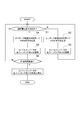
- FIG. 3 is a flowchart schematically illustrating an example of an operation method of the grid interconnection inverter device according to the embodiment.
- the control unit 14 of the grid interconnection inverter device 10 starts the operation and causes the instantaneous voltage drop detection unit 66 to detect an instantaneous voltage drop (step S ⁇ b> 1 in FIG. 3).
- the instantaneous voltage drop detection unit 66 detects an instantaneous voltage drop of the power system 4 based on the detection result of the AC voltage VAC input from the voltage detector 33 and inputs the detection result to the PWM controller 62.
- control unit 60 causes the control board 60 to start generating the voltage reference VR.
- the control board 60 generates a voltage reference VR based on the detection results of the voltage detectors 31 to 33, the detection results of the current detectors 36 to 38, the current command value, and the like, and the voltage reference VR is converted to the PWM controller 62. To enter.
- the PWM controller 62 When the instantaneous voltage drop is not detected, the PWM controller 62 generates a PWM signal using the unipolar modulation method, and inputs the PWM signal to the gate substrate 64 (step S2 in FIG. 3).
- the gate substrate 64 generates a gate signal of each switching element 40 of the three-level inverter 20 based on the input PWM signal, and inputs each gate signal to the control terminal of each switching element 40, whereby each switching element 40 is controlled on / off. That is, conversion from DC power to AC power by the three-level inverter 20 is controlled (step S3 in FIG. 3).
- the control unit 14 When the instantaneous voltage drop is not detected by the instantaneous drop detection unit 66, the control unit 14 repeatedly executes the processing of the above steps S1 to S3. Thereby, the DC power of the DC power source 2 is converted into AC power, and the AC power after conversion is supplied to the power system 4.
- the PWM controller 62 switches the modulation method from the unipolar modulation method to the dipolar modulation method when the instantaneous voltage drop is detected by the instantaneous voltage drop detection unit 66. At this time, the PWM controller 62 gradually changes from the unipolar modulation method to the dipolar modulation method over a predetermined time. Then, the PWM controller 62 generates a PWM signal using the dipolar modulation method, and inputs the PWM signal to the gate substrate 64 (step S4 in FIG. 3).
- the gate substrate 64 generates a gate signal for each switching element 40 from the PWM signal, and controls on / off of each switching element 40 (step S5 in FIG. 3).
- the control part 14 provides the FRT function which continues a driving
- the control unit 14 starts timing from the detection timing of the instantaneous voltage drop and determines whether or not a predetermined time has elapsed (see FIG. 3). Step S6).
- the predetermined time is, for example, 1 second.
- step S1 the control unit 14 returns to step S1. If the instantaneous voltage drop continues, the processing from step S4 to step S6 is repeated, and the operation of continuing operation when the instantaneous voltage drop occurs is executed. On the other hand, if a return from the instantaneous voltage drop is detected before the predetermined time has elapsed, the PWM controller 62 switches the modulation method from the dipolar modulation method to the unipolar modulation method, and the steps S1 to S3 are fixed. Return to normal operation.
- control unit 14 determines that a predetermined time has elapsed since the occurrence of the instantaneous voltage drop. In other words, the control unit 14 determines that the power system 4 is a system fault when a predetermined time has elapsed from the detection of the voltage drop, and stops the operation of the three-level inverter 20 in error.
- the operation of each switching element 40 of the three-level inverter 20 is controlled using the unipolar modulation method in a state where the occurrence of the instantaneous voltage drop is not detected.
- the operation of each switching element 40 of the three-level inverter 20 is controlled using the dipolar modulation method.
- the grid-connected inverter device 10 uses the unipolar modulation method when the modulation rate is high and uses the dipolar modulation method when the modulation rate is low.
- the modulation rate is a ratio between a direct-current voltage and an alternating-current voltage expressed by V AC (effective value) / V DC .
- the switching loss accompanying the on / off of each switching element 40 is increased as compared with the unipolar modulation method.
- the grid interconnection inverter device 10 uses a unipolar modulation method in a high modulation rate state where the occurrence of an instantaneous voltage drop is not detected. Thereby, in the grid connection inverter apparatus 10, the increase in the switching loss at the time of steady operation can be suppressed.
- the grid interconnection inverter device 10 uses a dipolar modulation method in a state where the occurrence of an instantaneous voltage drop is detected and the modulation rate is low. Thereby, in the grid connection inverter apparatus 10, generation
- the unipolar modulation method and the dipolar modulation method are switched according to the detection result of the instantaneous voltage drop. Thereby, switching loss can be suppressed and stable operation can be obtained.
- the operation is continued without a gate block for an instantaneous voltage drop with a residual voltage of 20% or more and a duration of less than 1 second, and within 0.1 seconds after the voltage is restored.
- it is required to return to an output of 80% or more before the voltage drop.
- the grid-connected inverter device 10 for example, when the residual voltage becomes less than 80%, the occurrence of the instantaneous voltage drop is detected, and the unipolar modulation system is detected within 0.1 second from the detection of the instantaneous voltage drop. The operation is switched to the dipolar modulation method and the operation is continued. When the residual voltage reaches 90% or more, the recovery from the instantaneous voltage drop is detected, and the dipolar modulation method to the unipolar modulation method is detected within 0.1 seconds after the return is detected. To output an AC voltage of 80% or more before the voltage drop. Thereby, in the grid connection inverter apparatus 10, the FRT function of photovoltaic power generation can be satisfy
- FIG. 4 is a block diagram schematically illustrating an example of a three-level inverter according to the embodiment.
- the three-level inverter INV ⁇ b> 1 (20) includes a plurality of switching elements 40, a plurality of rectifying elements 41 and 42, and a plurality of charge storage elements 43 and 44.
- the three-level inverter INV1 is a three-phase bridge type.
- the AC power of the power system 4 and the AC power converted by the three-level inverter INV1 are three-phase AC power.
- 3 level inverter INV1 has DC terminals 20p, 20n, AC terminals 20u, 20v, 20w, and six arms AU, AV, AW, AX, AY, AZ.
- the three-level inverter INV1 is connected to the DC power source 2 through the DC terminals 20p and 20n.
- the three-level inverter INV1 is connected to the power system 4 via AC terminals 20u, 20v, and 20w.
- Each arm AU, AV, AW, AX, AY, AZ is provided between the DC terminals 20p, 20n.
- the connection point between the arm AU and the arm AX, the connection point between the arm AV and the arm AY, and the connection point between the arm AW and the arm AZ are AC terminals 20u, 20v, and 20w, respectively.
- the three-level inverter INV1 includes twelve switching elements 40, twelve rectifying elements 41, six rectifying elements 42, and two charge storage elements 43 and 44.
- Each switching element 40 is connected in a three-phase bridge.
- Each rectifier element 41 is connected to each switching element 40 in antiparallel.
- the charge storage elements 43 and 44 are connected in series between the DC terminals 20p and 20n.
- the charge storage elements 43 and 44 are capacitors, for example. As a result, the connection point between the charge storage elements 43 and 44 becomes the neutral point 20c.
- each phase arm AU, AV, AW, AX, AY, AZ connected to each AC terminal 20u, 20v, 20w is substantially the same. Therefore, here, the two arms AU and AX connected to the AC terminal 20u (U phase) will be described as an example.
- the positive-side arm AU includes two switching elements Q1 and Q2 connected in series, rectifying elements DF1 and DF2 connected in antiparallel to the switching elements Q1 and Q2, and switching elements Q1 and Q2, respectively. And a rectifying element DC1 connected between the series connection point and the neutral point 20c.
- the negative arm AX includes two switching elements Q3 and Q4 connected in series, rectifying elements DF3 and DF4 connected in antiparallel to each of these switching elements Q3 and Q4, and each switching element.
- a rectifying element DC2 connected between the series connection point of Q3 and Q4 and the neutral point 20c.
- Both arms AU, AX are connected in series between DC terminals 20p, 20n, and the series connection point of both arms AU, AX is connected to U-phase AC terminal 20u.
- the potential at the series connection point of the switching elements Q1, Q2 is clamped to the neutral point potential via the rectifying element DC1.
- the potential at the series connection point of the switching elements Q3 and Q4 is clamped to the neutral point potential via the rectifying element DC2.
- the rectifying elements DF1 to DF4 (each rectifying element 41) are so-called reflux diodes.
- the rectifying elements DC1 and DC2 (each rectifying element 42) are so-called clamp diodes.
- the configuration of the arms AV and AW is substantially the same as the configuration of the arm AU.
- the configuration of the arms AY and AZ is substantially the same as the configuration of the arm AX.
- control is performed by switching between the unipolar modulation method and the dipolar modulation method according to the detection result of the instantaneous voltage drop. Thereby, switching loss can be suppressed and stable operation can be obtained.
- FIG. 5 is a block diagram schematically illustrating another example of the three-level inverter according to the embodiment.
- the three-level inverter INV ⁇ b> 2 (20) includes a plurality of switching elements 40, a plurality of rectifier elements 41, and a plurality of charge storage elements 43 and 44.
- the rectifying element 42 functioning as a clamp diode is omitted as compared with the three-level inverter INV1 described with reference to FIG. Note that components that are substantially the same in function and configuration as those of the three-level inverter INV1 described with reference to FIG.
- one switching element Q1, Q4 is provided for each of the arms AU, AX.
- Two switching elements Q2 and Q3 connected in series are provided between the AC terminal 20u and the neutral point 20c.
- the direction in which the current flows in the switching element Q2 is opposite to the direction in which the current flows in the switching element Q3.
- the switching element Q2 When the switching element Q2 is turned on, the direction of the current flowing through the switching element Q2 is a direction from the neutral point 20c toward the AC terminal 20u.
- the switching element Q3 When the switching element Q3 is turned on, the direction of the current flowing through the switching element Q3 is a direction from the AC terminal 20u toward the neutral point 20c. That is, the three-level inverter INV2 in this example is a so-called T-type NPC inverter.
- the three-level inverter INV2 similarly to the three-level inverter INV1, switching loss is suppressed and stable operation is obtained by switching between the unipolar modulation method and the dipolar modulation method according to the detection result of the instantaneous voltage drop. be able to.
- the three-level inverter 20 may have an arbitrary circuit configuration that can output a three-level voltage and can cope with the control using the unipolar modulation method and the control using the dipolar modulation method.
- the circuit configuration of the three-level inverter 20 is not limited to the three-level inverters INV1 and INV2, and can be changed as appropriate.
Landscapes
- Engineering & Computer Science (AREA)
- Power Engineering (AREA)
- Inverter Devices (AREA)
Abstract
3レベルインバータと電圧検出器と制御部とを備えた系統連系インバータ装置が提供される。3レベルインバータは、複数のスイッチング素子を有し、直流電源及び交流の電力系統に接続され、直流電源から供給された直流電力を各スイッチング素子のオン・オフによって直流電力から交流電力に変換し、交流電力を電力系統に供給する。電圧検出器は、電力系統の交流電圧を検出する。制御部は、電圧検出器の検出結果を基に、電力系統の瞬時電圧低下の検出を行い、瞬時電圧低下を検出していない状態では、ユニポーラ変調方式を用いて各スイッチング素子を制御し、瞬時電圧低下を検出している状態では、ダイポーラ変調方式を用いて各スイッチング素子を制御することにより、3レベルインバータによる直流電力から交流電力への変換を制御する。これにより、スイッチング損失を抑制し、安定した動作の系統連系インバータ装置が提供される。
Description
本発明の実施形態は、系統連系インバータ装置及びその運転方法に関する。
直流電力を交流電力に変換し、変換後の交流電力を交流電力系統に供給する系統連系インバータ装置がある。系統連系インバータ装置では、3レベルインバータを用い、3レベルの電圧を出力することが行われている。3レベルインバータは、複数のスイッチング素子を有する。3レベルインバータの各スイッチング素子のオン・オフは、例えば、3レベルPWM変調方式によって制御される。これにより、3レベルの電圧が出力される。3レベルインバータでは、2レベルインバータに比べて、出力電圧波形をより正弦波に近付けることができる。例えば、高調波成分を抑制し、出力側のフィルタの小型化を図ることができる。
3レベルPWM変調方式としては、例えば、正のパルス状電圧又は負のパルス状電圧を連続的に出力するユニポーラ変調方式や正負のパルス状電圧をゼロ電圧を介して交互に出力するダイポーラ変調方式などが知られている(例えば、非特許文献1)。ダイポーラ変調方式では、ユニポーラ変調方式に比べて、出力電圧の波形をより正弦波に近付けることができる。一方、ユニポーラ変調方式では、ダイポーラ変調方式に比べて、定常運転中の直流電圧の高い場合に、各スイッチング素子のオン・オフにともなうスイッチング損失を抑制することができる。
近年では、系統連系インバータ装置において、瞬時電圧低下などの一時的な交流電力系統の不具合が発生した場合にも、異常停止せずに動作を継続させるFRT(Fault Ride Through)機能が求められている。
FRT機能を有する系統連系インバータ装置にユニポーラ変調方式を用いると、瞬時電圧低下が発生して変調率が低くなった場合に、低次の高調波が発生し易くなってしまう。換言すれば、FRTの運転期間中に、出力電圧波形が歪んでしまう。ダイポーラ変調方式を用いた場合には、FRTの運転期間中における高調波の発生を抑制できる反面、定常運転中のスイッチング損失が増大してしまう。
このため、系統連系インバータ装置では、スイッチング損失を抑制しつつ、より安定した動作を得ることが望まれる。
福田昭治、鈴木邦生、「キャリア波を用いたマルチレベルPWM法の高調波特性評価」、電気学会論文誌D(産業応用部門誌)、119巻6号、平成11年、p.769-775
本発明の実施形態は、スイッチング損失を抑制し、かつ安定した動作の系統連系インバータ装置及びその運転方法を提供する。
本発明の実施形態によれば、3レベルインバータと、電圧検出器と、制御部と、を備えた系統連系インバータ装置が提供される。前記3レベルインバータは、複数のスイッチング素子を有し、直流電源及び交流の電力系統に接続され、前記直流電源から供給された直流電力を前記複数のスイッチング素子のオン・オフによって直流電力から交流電力に変換し、前記交流電力を前記電力系統に供給する。前記電圧検出器は、前記電力系統の交流電圧を検出する。前記制御部は、前記電圧検出器の検出結果を基に、前記電力系統の瞬時電圧低下の検出を行い、前記瞬時電圧低下を検出していない状態では、ユニポーラ変調方式を用いて前記複数のスイッチング素子の動作を制御し、前記瞬時電圧低下を検出している状態では、ダイポーラ変調方式を用いて前記複数のスイッチング素子の動作を制御することにより、前記3レベルインバータによる前記直流電力から前記交流電力への変換を制御する。
本発明の実施形態によれば、スイッチング損失を抑制し、かつ安定した動作の系統連系インバータ装置及びその運転方法が提供される。
以下に、各実施の形態について図面を参照しつつ説明する。
なお、図面は模式的または概念的なものであり、各部分の厚みと幅との関係、部分間の大きさの比率などは、必ずしも現実のものと同一とは限らない。また、同じ部分を表す場合であっても、図面により互いの寸法や比率が異なって表される場合もある。
なお、本願明細書と各図において、既出の図に関して前述したものと同様の要素には同一の符号を付して詳細な説明は適宜省略する。
なお、図面は模式的または概念的なものであり、各部分の厚みと幅との関係、部分間の大きさの比率などは、必ずしも現実のものと同一とは限らない。また、同じ部分を表す場合であっても、図面により互いの寸法や比率が異なって表される場合もある。
なお、本願明細書と各図において、既出の図に関して前述したものと同様の要素には同一の符号を付して詳細な説明は適宜省略する。
図1は、実施形態に係る系統連系インバータ装置を模式的に表すブロック図である。
図1に表したように、系統連系インバータ装置10は、主回路部12と、制御部14と、を備える。主回路部12は、3レベルインバータ20と、遮断器21、22と、フィルタコンデンサ24、25と、フィルタリアクトル26と、電圧検出器31~33と、電流検出器36~38と、を有する。
図1に表したように、系統連系インバータ装置10は、主回路部12と、制御部14と、を備える。主回路部12は、3レベルインバータ20と、遮断器21、22と、フィルタコンデンサ24、25と、フィルタリアクトル26と、電圧検出器31~33と、電流検出器36~38と、を有する。
3レベルインバータ20は、遮断器21を介して直流電源2に接続されている。また、3レベルインバータ20は、遮断器22を介して交流の電力系統4に接続されている。3レベルインバータ20は、直流電源2から供給される直流電力を交流電力に変換し、変換後の交流電力を電力系統4に供給する。
直流電源2は、例えば、太陽光発電機である。この場合、系統連系インバータ装置10は、パワーコンディショナーと呼ばれる場合もある。直流電源2は、太陽光発電機に限ることなく、直流電力を系統連系インバータ装置10に供給可能な任意の発電機や電源でよい。
電力系統4の交流電力は、単相交流電力でもよいし、三相交流電力などでもよい。3レベルインバータ20は、直流電力を単相交流電力に変換してもよいし、直流電力を三相交流電力に変換してもよい。
3レベルインバータ20は、各スイッチング素子40のオン・オフにより、直流電源2から供給された直流電力を交流電力に変換する。
3レベルインバータ20は、例えば、直流電源2から供給された直流電圧VDCを基に、0V、1/2VDC、VDCの3レベルの電圧を出力する。より詳しくは、-VDC、-1/2VDC、0V、1/2VDC、VDCの電圧を出力する。これにより、3レベルインバータ20は、直流電力を交流電力に変換する。3レベルインバータ20の回路構成は、3レベルの電圧を出力可能な任意の回路構成でよい。
各スイッチング素子40には、例えば、GTO(Gate Turn-Off thyristor)やIGBT(Insulated Gate Bipolar Transistor)などの自己消弧型の半導体素子が用いられる。各スイッチング素子40は、一対の主端子と、制御端子と、を有する。制御端子は、例えば、ゲート端子である。各スイッチング素子40は、制御端子の電圧に応じて、オン状態とオフ状態とを切り替える。各スイッチング素子40の制御端子は、制御部14に接続されている。制御部14は、各スイッチング素子40のオン・オフを切り替えることにより、3レベルインバータ20における直流電力から交流電力への変換を制御する。
遮断器21は、直流電源2と3レベルインバータ20との間に設けられている。遮断器21は、3レベルインバータ20を直流電源2に接続した状態と、3レベルインバータ20を直流電源2から切り離した状態と、を切り替える。遮断器22は、電力系統4と3レベルインバータ20との間に設けられている。遮断器22は、3レベルインバータ20を電力系統4に接続した状態と、3レベルインバータ20を電力系統4から切り離した状態と、を切り替える。各遮断器21、22の各状態の切り替えは、例えば、制御部14によって制御される。各遮断器21、22は、例えば、電流値や電圧値などに応じて自動的に各状態の切り替えを行ってもよい。各遮断器21、22は、必要に応じて設けられ、省略可能である。
フィルタコンデンサ24は、直流電源2と3レベルインバータ20との間に設けられる。この例において、フィルタコンデンサ24は、遮断器21と3レベルインバータ20との間に設けられる。フィルタコンデンサ24は、例えば、直流電源2からの直流電力に含まれるノイズを抑制する。換言すれば、フィルタコンデンサ24は、直流電圧を平滑化する。
フィルタコンデンサ25及びフィルタリアクトル26は、電力系統4と3レベルインバータ20との間に設けられる。この例において、フィルタコンデンサ25及びフィルタリアクトル26は、遮断器22と3レベルインバータ20との間に設けられる。
フィルタリアクトル26の一端は、3レベルインバータ20の交流出力端子に接続される。フィルタコンデンサ25及びフィルタリアクトル26は、3レベルインバータ20から出力される出力電圧VOUT及び出力電流IOUTの高調波成分を抑制し、出力電圧波形及び出力電流波形をより正弦波に近付ける。
この例では、便宜的に、1つのフィルタコンデンサ25及び1つのフィルタリアクトル26を図示している。例えば、電力系統4の交流電力が三相交流電力である場合には、フィルタコンデンサ25及びフィルタリアクトル26は、交流電力の各相に対応して設けられる。すなわち、三相交流電力の場合、フィルタコンデンサ25及びフィルタリアクトル26は、それぞれ3つずつ設けられる。
電圧検出器31は、直流電源2と遮断器21との間に設けられている。電圧検出器31は、制御部14に接続されている。電圧検出器31は、直流電源2の直流電圧VDCを検出し、検出結果を制御部14に入力する。
電圧検出器32は、フィルタリアクトル26と遮断器22との間に設けられている。電圧検出器32は、制御部14に接続されている。電圧検出器32は、3レベルインバータ20の出力電圧VOUTを検出し、検出結果を制御部14に入力する。
電圧検出器33は、遮断器22と電力系統4との間に設けられている。電圧検出器33は、制御部14に接続されている。電圧検出器33は、電力系統4の交流電圧VACを検出し、検出結果を制御部14に入力する。
また、3レベルインバータ20の出力電圧VOUT及び電力系統4の交流電圧VACが三相交流電圧である場合、電圧検出器32及び電圧検出器33は、三相交流電圧の各相の電圧値を検出し、検出結果を制御部14に入力する。
電流検出器36は、遮断器21と3レベルインバータ20との間に設けられている。電流検出器36は、制御部14に接続されている。電流検出器36は、直流電源2の直流電流IDCを検出し、検出結果を制御部14に入力する。
電流検出器37は、3レベルインバータ20とフィルタリアクトル26との間に設けられている。電流検出器37は、制御部14に接続されている。電流検出器37は、3レベルインバータ20の出力電流IOUTを検出し、検出結果を制御部14に入力する。
電流検出器38は、フィルタリアクトル26と遮断器22との間に設けられている。電流検出器38は、制御部14に接続されている。電流検出器38は、電力系統4の交流電流IACを検出し、検出結果を制御部14に入力する。
3レベルインバータ20の出力電流IOUT及び電力系統4の交流電流IACが三相交流電流である場合、電流検出器37及び電流検出器38は、三相交流電流の各相の電流値を検出し、検出結果を制御部14に入力する。
制御部14は、制御基板60と、PWM(Pulse Width Modulation)制御器62と、ゲート基板64と、瞬低検出部66と、を有する。制御基板60には、各電圧検出器31~33及び各電流検出器36~38のそれぞれの検出結果が入力される。また、制御基板60には、3レベルインバータ20の出力電流IOUTの電流指令値が入力される。出力電流IOUTの電流指令値は、換言すれば、電力系統4の交流電流IACの電流指令値である。電流指令値は、例えば、dq変換後の実効値換算値である。電流指令値は、例えば、正弦波状の信号でもよい。電流指令値は、予め決めれた一定の値でもよいし、上位のコントローラからの入力などによって変化させてもよい。
制御基板60は、入力された各電圧検出器31~33の検出結果、各電流検出器36~38の検出結果、及び電流指令値を基に、出力電流IOUTを電流指令値に近付けるための電圧基準VR(図2参照)を生成する。そして、制御基板60は、生成した電圧基準VRをPWM制御器62に入力する。電圧基準VRは、例えば、正弦波状の信号である。3レベルインバータ20の出力が三相交流電力である場合には、制御基板60は、各相毎に電圧基準VRを生成する。
PWM制御器62は、入力された電圧基準VRを基に、3レベルインバータ20の各スイッチング素子40のオン・オフを切り替えるためのPWM信号を生成する。PWM制御器62は、電圧基準VRとキャリア信号CS1、CS2(図2参照)とを比較することによって、PWM信号を生成する。キャリア信号CS1、CS2は、例えば、三角波状の信号である。PWM制御器62は、例えば、各スイッチング素子40に対応する複数のPWM信号を生成する。PWM制御器62は、生成した各PWM信号をゲート基板64に入力する。
ゲート基板64は、PWM制御器62に接続されるとともに、各スイッチング素子40の制御端子に接続されている。ゲート基板64は、入力された各PWM信号から各スイッチング素子40毎の複数のゲート信号(駆動信号)を生成し、生成した各ゲート信号を各スイッチング素子40のそれぞれの制御端子に入力する。これにより、制御部14は、各スイッチング素子40のオン・オフを制御する。
瞬低検出部66には、電圧検出器33による電力系統4の交流電圧VACの検出結果が入力される。瞬低検出部66は、入力された交流電圧VACの検出結果を基に、電力系統4の瞬時電圧低下の検出を行い、検出結果をPWM制御器62に入力する。瞬低検出部66は、例えば、交流電圧VACの残電圧が第1閾値未満になった場合に、電力系統4の瞬時電圧低下の発生を検出する。瞬低検出部66は、例えば、瞬時電圧低下を検出した後、交流電圧VACの残電圧が第2閾値以上になった場合に、電力系統4の瞬時電圧低下からの復帰を検出する。
残電圧とは、低下前の電圧に対する低下後の電圧の比率である。第1閾値は、例えば、80%である。第2閾値は、例えば、90%である。瞬低検出部66は、例えば、交流電圧VACの残電圧が80%未満になった場合に、電力系統4の瞬時電圧低下の発生を検出し、90%以上になった場合に、電力系統4の瞬時電圧低下からの復帰を検出する。このように、第2閾値は、第1閾値よりも大きくする。換言すれば、交流電圧VACの残電圧の判定にヒステリシスを持たせる。これにより、瞬低検出部66の出力が、瞬時電圧低下の検出状態と非検出状態とで交互に切り替わってしまうことを抑制することができる。なお、交流電圧VACの残電圧の判定は、必ずしもヒステリシスを持たなくてもよい。第2閾値は、第1閾値と同じでもよい。第2閾値は、第1閾値以上であればよい。
図2(a)及び図2(b)は、実施形態に係るPWM制御器の動作の一例を模式的に表すグラフ図である。
図2(a)は、PWM制御器62のユニポーラ変調方式の動作の一例を模式的に表す。図2(b)は、PWM制御器62のダイポーラ変調方式の動作の一例を模式的に表す。PWM制御器62は、ユニポーラ変調方式とダイポーラ変調方式とを用い、各方式を切り替えてPWM信号の生成を行う。
図2(a)は、PWM制御器62のユニポーラ変調方式の動作の一例を模式的に表す。図2(b)は、PWM制御器62のダイポーラ変調方式の動作の一例を模式的に表す。PWM制御器62は、ユニポーラ変調方式とダイポーラ変調方式とを用い、各方式を切り替えてPWM信号の生成を行う。
図2(a)及び図2(b)に表したように、PWM制御器62は、ユニポーラ変調方式及びダイポーラ変調方式のそれぞれにおいて、1つの電圧基準VRと、2つのキャリア信号CS1、CS2と、を用いる。キャリア信号CS2の直流バイアス成分は、キャリア信号CS1の直流バイアス成分と異なる。この例において、ユニポーラ変調方式は、換言すれば、ダブルキャリアユニポーラPWM方式であり、ダイポーラ変調方式は、換言すれば、ダブルキャリアダイポーラPWM方式である。
ユニポーラ変調方式において、キャリア信号CS1、CS2のそれぞれの振幅は、0.5である。また、ユニポーラ変調方式において、キャリア信号CS1の直流バイアス成分は、0.5であり、キャリア信号CS2の直流バイアス成分は、-0.5である。
ダイポーラ変調方式において、キャリア信号CS1、CS2のそれぞれの振幅は、1.0である。また、ダイポーラ変調方式において、キャリア信号CS1の直流バイアス成分は、0.5であり、キャリア信号CS2の直流バイアス成分は、-0.5である。
なお、各方式におけるキャリア信号CS1、CS2の振幅及び直流バイアス成分は、上記に限ることなく、3レベルインバータ20の動作を制御可能な範囲において、任意に設定可能である。各方式によるPWM信号の生成方法、及び3レベルインバータ20の各スイッチング素子40の制御方法については、例えば、上記の非特許文献1などに、より詳細に記載されている。
PWM制御器62は、瞬低検出部66の検出結果に応じて、ユニポーラ変調方式とダイポーラ変調方式とを切り替える。PWM制御器62は、瞬低検出部66が瞬時電圧低下を検出していない場合に、ユニポーラ変調方式を用いてPWM信号の生成を行う。そして、PWM制御器62は、瞬低検出部66が瞬時電圧低下を検出した場合に、ダイポーラ変調方式を用いてPWM信号の生成を行う。
PWM制御器62は、瞬低検出部66による瞬時電圧低下の検出に応じてユニポーラ変調方式からダイポーラ変調方式に切り替え、瞬時電圧低下からの復帰の検出に応じてダイポーラ変調方式からユニポーラ変調方式に切り替える。
PWM制御器62は、例えば、各キャリア信号CS1、CS2の振幅を変化させることによって、ユニポーラ変調方式とダイポーラ変調方式とを切り替える。PWM制御器62は、例えば、各キャリア信号CS1、CS2の振幅を0.5から1.0に変化させることにより、ユニポーラ変調方式からダイポーラ変調方式に切り替える。この際、PWM制御器62は、例えば、各キャリア信号CS1、CS2の振幅を所定時間かけて0.5から1.0に単調増加させることにより、ユニポーラ変調方式からダイポーラ変調方式に徐々に変化させる。これにより、変調方式の急変を抑制することができる。例えば、変調方式の急変にともなうノイズの発生などを抑制することができる。
同様に、PWM制御器62は、例えば、各キャリア信号CS1、CS2の振幅を所定時間かけて1.0から0.5に単調減少させることにより、ダイポーラ変調方式からユニポーラ変調方式に徐々に変化させる。
ユニポーラ変調方式とダイポーラ変調方式との切り替えは、各キャリア信号CS1、CS2の振幅に限ることなく、各キャリア信号CS1、CS2の直流バイアス成分を用いて行ってもよい。PWM制御器62は、例えば、各キャリア信号CS1、CS2の振幅及び直流バイアス成分の少なくとも一方を用いてユニポーラ変調方式とダイポーラ変調方式とを切り替える。ユニポーラ変調方式とダイポーラ変調方式との切り替えにおいては、例えば、電圧基準VRの振幅をさらに変化させてもよい。
ユニポーラ変調方式とダイポーラ変調方式との切り替えにおいては、例えば、各キャリア信号CS1、CS2の周波数(キャリア周波数)を変化させてもよい。ダイポーラ変調方式における各キャリア信号CS1、CS2の周波数は、例えば、ユニポーラ変調方式における各キャリア信号CS1、CS2の周波数の半分に設定する。これにより、例えば、3レベルインバータ20の各スイッチング素子40のスイッチング周波数を各方式間で実質的に同じにすることができる。
ユニポーラ変調方式とダイポーラ変調方式との切り替えにおいて、各キャリア信号CS1、CS2の振幅及び直流バイアス成分の少なくとも一方は、上記のように、徐々に変化させてもよいし、ユニポーラ変調方式の値とダイポーラ変調方式の値とに選択的に切り替えてもよい。振幅及び直流バイアス成分の少なくとも一方を徐々に変化させる場合、振幅及び直流バイアス成分の少なくとも一方の値は、連続的に変化させてもよいし、段階的に変化させてもよい。
また、振幅及び直流バイアス成分の少なくとも一方を徐々に変化させる場合、各方式の変化に要する所定時間は、0.1秒未満であることが好ましい。所定時間は、例えば、0.01秒以上0.1秒未満程度であることが好ましい。
図3は、実施形態に係る系統連系インバータ装置の運転方法の一例を模式的に表すフローチャートである。
図3に表したように、系統連系インバータ装置10の制御部14は、動作を開始すると、瞬低検出部66に瞬時電圧低下の検出を行わせる(図3のステップS1)。瞬低検出部66は、電圧検出器33から入力された交流電圧VACの検出結果を基に、電力系統4の瞬時電圧低下の検出を行い、検出結果をPWM制御器62に入力する。
図3に表したように、系統連系インバータ装置10の制御部14は、動作を開始すると、瞬低検出部66に瞬時電圧低下の検出を行わせる(図3のステップS1)。瞬低検出部66は、電圧検出器33から入力された交流電圧VACの検出結果を基に、電力系統4の瞬時電圧低下の検出を行い、検出結果をPWM制御器62に入力する。
また、制御部14は、動作を開始すると、制御基板60に電圧基準VRの生成を開始させる。制御基板60は、各電圧検出器31~33の検出結果、各電流検出器36~38の検出結果、及び電流指令値などに基づいて電圧基準VRを生成し、電圧基準VRをPWM制御器62に入力する。
PWM制御器62は、瞬時電圧低下が検出されていない場合、ユニポーラ変調方式を用いてPWM信号を生成し、PWM信号をゲート基板64に入力する(図3のステップS2)。
ゲート基板64は、入力されたPWM信号を基に、3レベルインバータ20の各スイッチング素子40のゲート信号を生成し、各ゲート信号を各スイッチング素子40の制御端子に入力することにより、各スイッチング素子40のオン・オフを制御する。すなわち、3レベルインバータ20による直流電力から交流電力への変換を制御する(図3のステップS3)。
制御部14は、瞬低検出部66によって瞬時電圧低下が検出されていない場合、上記のステップS1~ステップS3の処理を繰り返し実行する。これにより、直流電源2の直流電力が交流電力に変換され、変換後の交流電力が電力系統4に供給される。
一方、PWM制御器62は、瞬低検出部66によって瞬時電圧低下が検出された場合、変調方式をユニポーラ変調方式からダイポーラ変調方式に切り替える。この際、PWM制御器62は、ユニポーラ変調方式からダイポーラ変調方式に所定時間かけて徐々に変化させる。そして、PWM制御器62は、ダイポーラ変調方式を用いてPWM信号を生成し、PWM信号をゲート基板64に入力する(図3のステップS4)。
ゲート基板64は、ステップS3と同様に、PWM信号から各スイッチング素子40のゲート信号を生成し、各スイッチング素子40のオン・オフを制御する(図3のステップS5)。これにより、制御部14は、瞬時電圧低下の発生時にも運転を継続するFRT機能を提供する。より詳しくは、LVRT(Low Voltage Ride Through)機能を提供する。
制御部14は、瞬低検出部66によって瞬時電圧低下の発生が検出された場合、瞬時電圧低下の検出のタイミングから計時を開始し、所定時間が経過したか否かを判定する(図3のステップS6)。所定時間は、例えば、1秒である。
所定時間が経過していない場合、制御部14は、ステップS1に戻る。瞬時電圧低下が継続している場合には、ステップS4~ステップS6の処理が繰り返され、瞬時電圧低下の発生時の運転継続の動作が実行される。一方、所定時間の経過の前に、瞬時電圧低下からの復帰が検出された場合には、PWM制御器62が、変調方式をダイポーラ変調方式からユニポーラ変調方式に切り替え、ステップS1~ステップS3の定常時の動作に戻る。
制御部14は、瞬時電圧低下の発生から所定時間が経過したと判定した場合、3レベルインバータ20の各スイッチング素子40の制御を停止する。換言すれば、制御部14は、電圧低下の検出から所定時間経過した場合には、電力系統4の系統事故であると判断し、3レベルインバータ20の動作をエラー停止させる。
このように、本実施形態に係る系統連系インバータ装置10では、瞬時電圧低下の発生を検出していない状態では、ユニポーラ変調方式を用いて3レベルインバータ20の各スイッチング素子40の動作を制御し、瞬時電圧低下の発生を検出している状態では、ダイポーラ変調方式を用いて3レベルインバータ20の各スイッチング素子40の動作を制御する。換言すれば、系統連系インバータ装置10は、変調率の高い状態においては、ユニポーラ変調方式を用い、変調率の低い状態においては、ダイポーラ変調方式を用いる。なお、変調率は、VAC(実効値)/VDCで表される直流電圧と交流電圧との比率である。
ダイポーラ変調方式では、変調率が高い場合(例えば0.5以上)に、ユニポーラ変調方式に比べて各スイッチング素子40のオン・オフにともなうスイッチング損失が増大してしまう。系統連系インバータ装置10は、瞬時電圧低下の発生を検出していない変調率の高い状態において、ユニポーラ変調方式を用いる。これにより、系統連系インバータ装置10では、定常運転時におけるスイッチング損失の増大を抑制することができる。
また、ユニポーラ変調方式では、変調率が低い場合(例えば0.5未満)に、ダイポーラ変調方式に比べて低次の高調波が発生し易くなってしまう。系統連系インバータ装置10は、瞬時電圧低下の発生を検出している変調率の低い状態において、ダイポーラ変調方式を用いる。これにより、系統連系インバータ装置10では、FRTの運転期間中における高調波の発生を抑制することができる。例えば、FRTの運転期間中においても、正弦波に近い波形を出力し、安定した動作を得ることができる。
このように、本実施形態に係る系統連系インバータ装置10では、瞬時電圧低下の検出結果に応じて、ユニポーラ変調方式とダイポーラ変調方式とを切り替える。これにより、スイッチング損失を抑制し、かつ安定した動作を得ることができる。
例えば、太陽光発電のFRT機能では、残電圧が20%以上で継続時間が1秒以内の瞬時電圧低下に対して、ゲートブロックせずに運転継続を行い、電圧の復帰後0.1秒以内に、電圧低下前の80%以上の出力に復帰することが求められている。
これに対して、系統連系インバータ装置10では、例えば、残電圧が80%未満になった場合に瞬時電圧低下の発生を検出し、瞬時電圧低下の検出から0.1秒以内にユニポーラ変調方式からダイポーラ変調方式に切り替えて運転を継続し、残電圧が90%以上になった場合に瞬時電圧低下からの復帰を検出し、復帰の検出から0.1秒以内にダイポーラ変調方式からユニポーラ変調方式に切り替えて、電圧低下前の80%以上の交流電圧を出力する。これにより、系統連系インバータ装置10において、太陽光発電のFRT機能を満たすことができる。
図4は、実施形態に係る3レベルインバータの一例を模式的に表すブロック図である。図4に表したように、3レベルインバータINV1(20)は、複数のスイッチング素子40と、複数の整流素子41、42と、複数の電荷蓄積素子43、44と、を有する。この例において、3レベルインバータINV1は、三相ブリッジ型である。この例において、電力系統4の交流電力及び3レベルインバータINV1の変換する交流電力は、三相交流電力である。
3レベルインバータINV1は、直流端子20p、20nと、交流端子20u、20v、20wと、6つのアームAU、AV、AW、AX、AY、AZと、を有する。3レベルインバータINV1は、直流端子20p、20nを介して直流電源2に接続される。そして、3レベルインバータINV1は、交流端子20u、20v、20wを介して電力系統4に接続される。
各アームAU、AV、AW、AX、AY、AZは、直流端子20p、20nの間に設けられる。3レベルインバータINV1では、アームAUとアームAXとの接続点、アームAVとアームAYとの接続点、及びアームAWとアームAZとの接続点のそれぞれが、交流端子20u、20v、20wになる。
この例において、3レベルインバータINV1は、12個のスイッチング素子40と、12個の整流素子41と、6個の整流素子42と、2個の電荷蓄積素子43、44と、を有する。各スイッチング素子40は、三相ブリッジ接続されている。各整流素子41は、各スイッチング素子40に逆並列に接続されている。電荷蓄積素子43、44は、直流端子20p、20nの間に直列に接続されている。電荷蓄積素子43、44は、例えば、コンデンサである。これにより、電荷蓄積素子43、44の接続点が、中性点20cになる。
各交流端子20u、20v、20wに接続される各相のアームAU、AV、AW、AX、AY、AZのそれぞれの構成は、実質的に同じである。従って、ここでは例示として交流端子20u(U相)に接続される2つのアームAU、AXについて説明する。
正側のアームAUは、直列に接続された2つのスイッチング素子Q1、Q2と、これらのスイッチング素子Q1、Q2のそれぞれに逆並列に接続された整流素子DF1、DF2と、各スイッチング素子Q1、Q2の直列接続点と中性点20cとの間に接続された整流素子DC1と、を有する。
同様に、負側のアームAXは、直列に接続された2つのスイッチング素子Q3、Q4と、これらのスイッチング素子Q3、Q4のそれぞれに逆並列に接続された整流素子DF3、DF4と、各スイッチング素子Q3、Q4の直列接続点と中性点20cとの間に接続された整流素子DC2と、を有する。
両アームAU、AXは、直流端子20p、20nとの間に直列に接続され、両アームAU、AXの直列接続点がU相の交流端子20uに接続される。スイッチング素子Q1、Q2の直列接続点の電位は、整流素子DC1を介して中性点電位にクランプされる。同様に、スイッチング素子Q3、Q4の直列接続点の電位は、整流素子DC2を介して中性点電位にクランプされる。整流素子DF1~DF4(各整流素子41)は、いわゆる還流ダイオードである。整流素子DC1、DC2(各整流素子42)は、いわゆるクランプダイオードである。
アームAV、AWの構成は、アームAUの構成と実質的に同じである。アームAY、AZの構成は、アームAXの構成と実質的に同じである。これにより、各スイッチング素子40のスイッチングに応じて、交流端子20u、20v、20wの電位が、直流端子20p、直流端子20n、及び中性点20cの3レベルのいずれかの電位にクランプされる。3レベルインバータINV1は、いわゆる中性点クランプ型の変換器である。3レベルインバータINV1は、いわゆるNPC(NPC:Neutral-Point-Clamped)インバータである。
このようなNPC型の3レベルインバータINV1において、上述のように、瞬時電圧低下の検出結果に応じて、ユニポーラ変調方式とダイポーラ変調方式とを切り替えて制御を行う。これにより、スイッチング損失を抑制し、かつ安定した動作を得ることができる。
図5は、実施形態に係る3レベルインバータの別の一例を模式的に表すブロック図である。
図5に表したように、3レベルインバータINV2(20)は、複数のスイッチング素子40と、複数の整流素子41と、複数の電荷蓄積素子43、44と、を有する。3レベルインバータINV2では、図4に関して説明した3レベルインバータINV1に比べて、クランプダイオードとして機能する整流素子42が省略されている。なお、図4に関して説明した3レベルインバータINV1と機能・構成上実質的に同じものについては、同符号を付し、詳細な説明は省略する。
図5に表したように、3レベルインバータINV2(20)は、複数のスイッチング素子40と、複数の整流素子41と、複数の電荷蓄積素子43、44と、を有する。3レベルインバータINV2では、図4に関して説明した3レベルインバータINV1に比べて、クランプダイオードとして機能する整流素子42が省略されている。なお、図4に関して説明した3レベルインバータINV1と機能・構成上実質的に同じものについては、同符号を付し、詳細な説明は省略する。
この例では、アームAU、AXのそれぞれに、1つのスイッチング素子Q1、Q4が設けられる。そして、交流端子20uと中性点20cとの間に、直列に接続された2つのスイッチング素子Q2、Q3が設けられる。
スイッチング素子Q2において電流の流れる向きは、スイッチング素子Q3において電流の流れる向きと反対である。スイッチング素子Q2をオン状態にした時に、スイッチング素子Q2に流れる電流の向きは、中性点20cから交流端子20uに向かう方向である。スイッチング素子Q3をオン状態にした時に、スイッチング素子Q3に流れる電流の向きは、交流端子20uから中性点20cに向かう方向である。すなわち、この例における3レベルインバータINV2は、いわゆるT型NPCインバータである。
3レベルインバータINV2においても、3レベルインバータINV1と同様に、瞬時電圧低下の検出結果に応じて、ユニポーラ変調方式とダイポーラ変調方式とを切り替えることにより、スイッチング損失を抑制し、かつ安定した動作を得ることができる。
このように、3レベルインバータ20は、3レベルの電圧を出力可能であり、かつユニポーラ変調方式を用いた制御とダイポーラ変調方式を用いた制御とに対応可能な任意の回路構成でよい。3レベルインバータ20の回路構成は、上記の3レベルインバータINV1、INV2に限ることなく、適宜変更可能である。
以上、具体例を参照しつつ、本発明の実施の形態について説明した。しかし、本発明の実施形態は、これらの具体例に限定されるものではない。例えば、系統連系インバータ装置に含まれる、3レベルインバータ、電圧検出器、及び制御部などの各要素の具体的な構成に関しては、当業者が公知の範囲から適宜選択することにより本発明を同様に実施し、同様の効果を得ることができる限り、本発明の範囲に包含される。
また、各具体例のいずれか2つ以上の要素を技術的に可能な範囲で組み合わせたものも、本発明の要旨を包含する限り本発明の範囲に含まれる。
また、各具体例のいずれか2つ以上の要素を技術的に可能な範囲で組み合わせたものも、本発明の要旨を包含する限り本発明の範囲に含まれる。
その他、本発明の実施の形態として上述した系統連系インバータ装置及びその運転方法を基にして、当業者が適宜設計変更して実施し得る全ての系統連系インバータ装置及びその運転方法も、本発明の要旨を包含する限り、本発明の範囲に属する。
その他、本発明の思想の範疇において、当業者であれば、各種の変更例及び修正例に想到し得るものであり、それら変更例及び修正例についても本発明の範囲に属するものと了解される。
本発明のいくつかの実施形態を説明したが、これらの実施形態は、例として提示したものであり、発明の範囲を限定することは意図していない。これら新規な実施形態は、その他の様々な形態で実施されることが可能であり、発明の要旨を逸脱しない範囲で、種々の省略、置き換え、変更を行うことができる。これら実施形態やその変形は、発明の範囲や要旨に含まれるとともに、請求の範囲に記載された発明とその均等の範囲に含まれる。
Claims (5)
- 複数のスイッチング素子を有し、直流電源及び交流の電力系統に接続され、前記直流電源から供給された直流電力を前記複数のスイッチング素子のオン・オフによって直流電力から交流電力に変換し、前記交流電力を前記電力系統に供給する3レベルインバータと、
前記電力系統の交流電圧を検出する電圧検出器と、
前記電圧検出器の検出結果を基に、前記電力系統の瞬時電圧低下の検出を行い、前記瞬時電圧低下を検出していない状態では、ユニポーラ変調方式を用いて前記複数のスイッチング素子の動作を制御し、前記瞬時電圧低下を検出している状態では、ダイポーラ変調方式を用いて前記複数のスイッチング素子の動作を制御することにより、前記3レベルインバータによる前記直流電力から前記交流電力への変換を制御する制御部と、
を備えた系統連系インバータ装置。 - 前記制御部は、前記ユニポーラ変調方式と前記ダイポーラ変調方式とのそれぞれにおいて、直流バイアス成分の異なる三角波状の2つのキャリア信号と、正弦波状の電圧基準と、を用い、前記2つのキャリア信号と前記電圧基準との比較によって前記複数のスイッチング素子の動作を制御し、前記2つのキャリア信号のそれぞれの振幅及び直流バイアス成分の少なくとも一方を所定時間かけて変化させることにより、前記ユニポーラ変調方式から前記ダイポーラ変調方式に又は前記ダイポーラ変調方式から前記ユニポーラ変調方式に徐々に変化させる請求項1記載の系統連系インバータ装置。
- 前記制御部は、前記電圧検出器によって検出された前記交流電圧の残電圧が第1閾値未満になった場合に、前記瞬時電圧低下の発生を検出し、前記瞬時電圧低下を検出した後、前記交流電圧の残電圧が第2閾値以上になった場合に、前記瞬時電圧低下からの復帰を検出し、
前記第2閾値は、前記第1閾値よりも大きい請求項1記載の系統連系インバータ装置。 - 前記制御部は、前記瞬時電圧低下の検出のタイミングから所定時間の計時を開始し、前記所定時間の経過の前に前記瞬時電圧低下からの復帰が検出された場合には、前記ダイポーラ変調方式から前記ユニポーラ変調方式に切り替えて定常時の動作に戻り、前記所定時間が経過した場合には、前記複数のスイッチング素子の制御を停止する請求項1記載の系統連系インバータ装置。
- 複数のスイッチング素子を有し、直流電源及び交流の電力系統に接続され、前記直流電源から供給された直流電力を前記複数のスイッチング素子のオン・オフによって直流電力から交流電力に変換し、前記交流電力を前記電力系統に供給する3レベルインバータと、
前記電力系統の交流電圧を検出する電圧検出器と、
を備えた系統連系インバータ装置の運転方法であって、
前記電圧検出器の検出結果を基に、前記電力系統の瞬時電圧低下の検出を行う工程と、
前記瞬時電圧低下を検出していない状態では、ユニポーラ変調方式を用いて前記複数のスイッチング素子の動作を制御し、前記瞬時電圧低下を検出している状態では、ダイポーラ変調方式を用いて前記複数のスイッチング素子の動作を制御することにより、前記3レベルインバータによる前記直流電力から前記交流電力への変換を制御する工程と、
を有する系統連系インバータ装置の運転方法。
Priority Applications (4)
| Application Number | Priority Date | Filing Date | Title |
|---|---|---|---|
| JP2018534225A JP6666058B2 (ja) | 2016-08-16 | 2016-08-16 | 系統連系インバータ装置及びその運転方法 |
| US16/324,737 US20190190403A1 (en) | 2016-08-16 | 2016-08-16 | System-connected inverter device and method for operating same |
| PCT/JP2016/073928 WO2018033964A1 (ja) | 2016-08-16 | 2016-08-16 | 系統連系インバータ装置及びその運転方法 |
| CN201680088496.XA CN109769404B (zh) | 2016-08-16 | 2016-08-16 | 系统互连逆变器装置及其运转方法 |
Applications Claiming Priority (1)
| Application Number | Priority Date | Filing Date | Title |
|---|---|---|---|
| PCT/JP2016/073928 WO2018033964A1 (ja) | 2016-08-16 | 2016-08-16 | 系統連系インバータ装置及びその運転方法 |
Publications (1)
| Publication Number | Publication Date |
|---|---|
| WO2018033964A1 true WO2018033964A1 (ja) | 2018-02-22 |
Family
ID=61196546
Family Applications (1)
| Application Number | Title | Priority Date | Filing Date |
|---|---|---|---|
| PCT/JP2016/073928 Ceased WO2018033964A1 (ja) | 2016-08-16 | 2016-08-16 | 系統連系インバータ装置及びその運転方法 |
Country Status (4)
| Country | Link |
|---|---|
| US (1) | US20190190403A1 (ja) |
| JP (1) | JP6666058B2 (ja) |
| CN (1) | CN109769404B (ja) |
| WO (1) | WO2018033964A1 (ja) |
Cited By (4)
| Publication number | Priority date | Publication date | Assignee | Title |
|---|---|---|---|---|
| DE102019105196A1 (de) * | 2019-02-28 | 2020-09-03 | Sma Solar Technology Ag | Verfahren zur Strombegrenzung bei transienten Spannungsänderungen an einem Wechselstromausgang eines Multilevel-Wechselrichters und Multilevel-Wechselrichter |
| WO2020255338A1 (ja) * | 2019-06-20 | 2020-12-24 | 東芝三菱電機産業システム株式会社 | 電力変換装置 |
| CN112953274A (zh) * | 2019-11-26 | 2021-06-11 | 新疆金风科技股份有限公司 | 功率模块及其控制方法 |
| JP2023513857A (ja) * | 2021-01-19 | 2023-04-04 | ファーウェイ デジタル パワー テクノロジーズ カンパニー リミテッド | 故障保護装置及び太陽光発電システム |
Families Citing this family (5)
| Publication number | Priority date | Publication date | Assignee | Title |
|---|---|---|---|---|
| US10826381B2 (en) * | 2018-04-17 | 2020-11-03 | Abb Schweiz Ag | Method and control system for zero-sequence current compensation for ground current reduction |
| US10910955B2 (en) * | 2019-01-18 | 2021-02-02 | Tsinghua University | Single carrier based multilevel modulation method and device, and storage medium |
| CN115411918A (zh) * | 2022-08-10 | 2022-11-29 | 华为数字能源技术有限公司 | 逆变器及其控制方法、以及供电系统 |
| US20240326149A1 (en) * | 2023-04-03 | 2024-10-03 | The Esab Group, Inc. | Controlling on-time of pwm applied to power blocks in welding system |
| DE102023004903B3 (de) * | 2023-11-29 | 2025-03-06 | Mercedes-Benz Group AG | Verfahren zum Betreiben eines Wechselrichters |
Citations (5)
| Publication number | Priority date | Publication date | Assignee | Title |
|---|---|---|---|---|
| JPH05344739A (ja) * | 1992-06-04 | 1993-12-24 | Hitachi Ltd | 電力変換装置 |
| JPH09149658A (ja) * | 1995-11-24 | 1997-06-06 | Hitachi Ltd | 直列多重型インバータ装置 |
| JP2009165265A (ja) * | 2008-01-07 | 2009-07-23 | Mitsubishi Electric Corp | 電力変換装置 |
| JP2012070498A (ja) * | 2010-09-22 | 2012-04-05 | Daihen Corp | インバータ装置、および、このインバータ装置を備えた系統連系インバータシステム |
| JP2015192562A (ja) * | 2014-03-28 | 2015-11-02 | 株式会社東芝 | 電力変換装置 |
Family Cites Families (7)
| Publication number | Priority date | Publication date | Assignee | Title |
|---|---|---|---|---|
| WO2011150962A1 (en) * | 2010-06-01 | 2011-12-08 | Abb Technology Ag | Interface arrangement between ac and dc systems including filter at transformer neutral point |
| CN101977019B (zh) * | 2010-10-29 | 2012-07-25 | 中国兵器工业集团第二一四研究所苏州研发中心 | 一种支持单双极脉宽调制控制的h桥电机控制器 |
| DE102011051548A1 (de) * | 2011-07-04 | 2013-01-10 | Sma Solar Technology Ag | Betriebsverfahren für einen Wechselrichter und netzfehlertoleranter Wechselrichter |
| CN102790399B (zh) * | 2012-07-25 | 2015-09-09 | 华为技术有限公司 | 电网无功补偿方法、装置及并网逆变器 |
| CN102840160B (zh) * | 2012-09-28 | 2014-12-24 | 江苏省电力公司常州供电公司 | 风冷控制装置及其工作方法 |
| US9356536B2 (en) * | 2013-01-11 | 2016-05-31 | ABBI Research Ltd. | Bidirectional power conversion with fault-handling capability |
| JP6030263B1 (ja) * | 2016-06-30 | 2016-11-24 | 田淵電機株式会社 | 系統連系用電力変換装置、及びその出力電流制御方法 |
-
2016
- 2016-08-16 US US16/324,737 patent/US20190190403A1/en not_active Abandoned
- 2016-08-16 WO PCT/JP2016/073928 patent/WO2018033964A1/ja not_active Ceased
- 2016-08-16 JP JP2018534225A patent/JP6666058B2/ja active Active
- 2016-08-16 CN CN201680088496.XA patent/CN109769404B/zh active Active
Patent Citations (5)
| Publication number | Priority date | Publication date | Assignee | Title |
|---|---|---|---|---|
| JPH05344739A (ja) * | 1992-06-04 | 1993-12-24 | Hitachi Ltd | 電力変換装置 |
| JPH09149658A (ja) * | 1995-11-24 | 1997-06-06 | Hitachi Ltd | 直列多重型インバータ装置 |
| JP2009165265A (ja) * | 2008-01-07 | 2009-07-23 | Mitsubishi Electric Corp | 電力変換装置 |
| JP2012070498A (ja) * | 2010-09-22 | 2012-04-05 | Daihen Corp | インバータ装置、および、このインバータ装置を備えた系統連系インバータシステム |
| JP2015192562A (ja) * | 2014-03-28 | 2015-11-02 | 株式会社東芝 | 電力変換装置 |
Cited By (12)
| Publication number | Priority date | Publication date | Assignee | Title |
|---|---|---|---|---|
| DE102019105196A1 (de) * | 2019-02-28 | 2020-09-03 | Sma Solar Technology Ag | Verfahren zur Strombegrenzung bei transienten Spannungsänderungen an einem Wechselstromausgang eines Multilevel-Wechselrichters und Multilevel-Wechselrichter |
| DE102019105196B4 (de) * | 2019-02-28 | 2021-01-07 | Sma Solar Technology Ag | Verfahren zur Strombegrenzung bei transienten Spannungsänderungen an einem Wechselstromausgang eines Multilevel-Wechselrichters und Multilevel-Wechselrichter |
| US11621650B2 (en) | 2019-02-28 | 2023-04-04 | Sma Solar Technology Ag | Method for current limitation in the event of transient voltage variations at an AC output of a multi-level inverter and a multi-level inverter |
| WO2020255338A1 (ja) * | 2019-06-20 | 2020-12-24 | 東芝三菱電機産業システム株式会社 | 電力変換装置 |
| CN112492892A (zh) * | 2019-06-20 | 2021-03-12 | 东芝三菱电机产业系统株式会社 | 电力变换装置 |
| JPWO2020255338A1 (ja) * | 2019-06-20 | 2021-09-13 | 東芝三菱電機産業システム株式会社 | 電力変換装置 |
| CN112492892B (zh) * | 2019-06-20 | 2023-08-04 | 东芝三菱电机产业系统株式会社 | 电力变换装置 |
| CN112953274A (zh) * | 2019-11-26 | 2021-06-11 | 新疆金风科技股份有限公司 | 功率模块及其控制方法 |
| JP2023513857A (ja) * | 2021-01-19 | 2023-04-04 | ファーウェイ デジタル パワー テクノロジーズ カンパニー リミテッド | 故障保護装置及び太陽光発電システム |
| US11811217B2 (en) | 2021-01-19 | 2023-11-07 | Huawei Digital Power Technologies Co., Ltd. | Fault protection apparatus and photovoltaic power generation system |
| JP7405948B2 (ja) | 2021-01-19 | 2023-12-26 | ファーウェイ デジタル パワー テクノロジーズ カンパニー リミテッド | 故障保護装置及び太陽光発電システム |
| US12567733B2 (en) | 2021-01-19 | 2026-03-03 | Huawei Digital Power Technologies Co., Ltd. | Fault protection apparatus and photovoltaic inverter |
Also Published As
| Publication number | Publication date |
|---|---|
| CN109769404B (zh) | 2021-02-26 |
| CN109769404A (zh) | 2019-05-17 |
| US20190190403A1 (en) | 2019-06-20 |
| JPWO2018033964A1 (ja) | 2019-06-13 |
| JP6666058B2 (ja) | 2020-03-13 |
Similar Documents
| Publication | Publication Date | Title |
|---|---|---|
| JP6666058B2 (ja) | 系統連系インバータ装置及びその運転方法 | |
| US9048754B2 (en) | System and method for offsetting the input voltage unbalance in multilevel inverters or the like | |
| Choudhury et al. | A hybrid PWM-based DC-link voltage balancing algorithm for a three-level NPC DC/AC traction inverter drive | |
| US9013906B2 (en) | Power system-interconnected inverter device | |
| CN103650320B (zh) | 用于运行逆变器的方法和能容忍电网错误的逆变器 | |
| JP5788017B2 (ja) | 電力変換装置 | |
| JP5223711B2 (ja) | 無停電電源装置 | |
| JP6087531B2 (ja) | 電力変換装置 | |
| WO2007129456A1 (ja) | 電力変換装置 | |
| Lee et al. | An improved phase-shifted PWM method for a three-phase cascaded H-bridge multi-level inverter | |
| JP5374336B2 (ja) | 電力変換装置 | |
| CN110521102B (zh) | 电力转换装置 | |
| JP2013179781A (ja) | 変換器、変換器の制御方法及び変換器の制御プログラム | |
| JP6158125B2 (ja) | 電力変換装置 | |
| JP2014007846A (ja) | 電力変換装置 | |
| JP5734083B2 (ja) | 電力変換装置 | |
| Aly et al. | An efficient neutral point voltage control algorithm with reduced switching losses for three level inverters | |
| JP5490263B2 (ja) | 電力変換装置 | |
| JP2016063687A (ja) | 電力変換装置 | |
| Kumar et al. | Simulation analysis of a nearest level modulation scheme for cross-connected sources based MLI | |
| US20200228028A1 (en) | Inverter system | |
| CN110463011B (zh) | 电力转换装置 | |
| Pradhan et al. | Single phase dynamic voltage restorer topology based on five-level ground point shifting inverter | |
| Itoh et al. | Experimental verification of a multi-level inverter with H-bridge clamp circuit for single-phase three-wire grid connection | |
| JP2019176647A (ja) | インバータ装置 |
Legal Events
| Date | Code | Title | Description |
|---|---|---|---|
| 121 | Ep: the epo has been informed by wipo that ep was designated in this application |
Ref document number: 16913493 Country of ref document: EP Kind code of ref document: A1 |
|
| ENP | Entry into the national phase |
Ref document number: 2018534225 Country of ref document: JP Kind code of ref document: A |
|
| NENP | Non-entry into the national phase |
Ref country code: DE |
|
| 122 | Ep: pct application non-entry in european phase |
Ref document number: 16913493 Country of ref document: EP Kind code of ref document: A1 |