WO2018029928A1 - 電力変換装置 - Google Patents
電力変換装置 Download PDFInfo
- Publication number
- WO2018029928A1 WO2018029928A1 PCT/JP2017/017860 JP2017017860W WO2018029928A1 WO 2018029928 A1 WO2018029928 A1 WO 2018029928A1 JP 2017017860 W JP2017017860 W JP 2017017860W WO 2018029928 A1 WO2018029928 A1 WO 2018029928A1
- Authority
- WO
- WIPO (PCT)
- Prior art keywords
- discharge
- load
- voltage
- power converter
- switch
- Prior art date
- Legal status (The legal status is an assumption and is not a legal conclusion. Google has not performed a legal analysis and makes no representation as to the accuracy of the status listed.)
- Ceased
Links
Images




Classifications
-
- H—ELECTRICITY
- H02—GENERATION; CONVERSION OR DISTRIBUTION OF ELECTRIC POWER
- H02M—APPARATUS FOR CONVERSION BETWEEN AC AND AC, BETWEEN AC AND DC, OR BETWEEN DC AND DC, AND FOR USE WITH MAINS OR SIMILAR POWER SUPPLY SYSTEMS; CONVERSION OF DC OR AC INPUT POWER INTO SURGE OUTPUT POWER; CONTROL OR REGULATION THEREOF
- H02M3/00—Conversion of DC power input into DC power output
- H02M3/22—Conversion of DC power input into DC power output with intermediate conversion into AC
- H02M3/24—Conversion of DC power input into DC power output with intermediate conversion into AC by static converters
- H02M3/28—Conversion of DC power input into DC power output with intermediate conversion into AC by static converters using discharge tubes with control electrode or semiconductor devices with control electrode to produce the intermediate AC
- H02M3/325—Conversion of DC power input into DC power output with intermediate conversion into AC by static converters using discharge tubes with control electrode or semiconductor devices with control electrode to produce the intermediate AC using devices of a triode or a transistor type requiring continuous application of a control signal
- H02M3/335—Conversion of DC power input into DC power output with intermediate conversion into AC by static converters using discharge tubes with control electrode or semiconductor devices with control electrode to produce the intermediate AC using devices of a triode or a transistor type requiring continuous application of a control signal using semiconductor devices only
- H02M3/33507—Conversion of DC power input into DC power output with intermediate conversion into AC by static converters using discharge tubes with control electrode or semiconductor devices with control electrode to produce the intermediate AC using devices of a triode or a transistor type requiring continuous application of a control signal using semiconductor devices only with automatic control of the output voltage or current, e.g. flyback converters
- H02M3/33523—Conversion of DC power input into DC power output with intermediate conversion into AC by static converters using discharge tubes with control electrode or semiconductor devices with control electrode to produce the intermediate AC using devices of a triode or a transistor type requiring continuous application of a control signal using semiconductor devices only with automatic control of the output voltage or current, e.g. flyback converters with galvanic isolation between input and output of both the power stage and the feedback loop
-
- F—MECHANICAL ENGINEERING; LIGHTING; HEATING; WEAPONS; BLASTING
- F16—ENGINEERING ELEMENTS AND UNITS; GENERAL MEASURES FOR PRODUCING AND MAINTAINING EFFECTIVE FUNCTIONING OF MACHINES OR INSTALLATIONS; THERMAL INSULATION IN GENERAL
- F16F—SPRINGS; SHOCK-ABSORBERS; MEANS FOR DAMPING VIBRATION
- F16F1/00—Springs
- F16F1/36—Springs made of rubber or other material having high internal friction, e.g. thermoplastic elastomers
- F16F1/3605—Springs made of rubber or other material having high internal friction, e.g. thermoplastic elastomers characterised by their material
-
- F—MECHANICAL ENGINEERING; LIGHTING; HEATING; WEAPONS; BLASTING
- F16—ENGINEERING ELEMENTS AND UNITS; GENERAL MEASURES FOR PRODUCING AND MAINTAINING EFFECTIVE FUNCTIONING OF MACHINES OR INSTALLATIONS; THERMAL INSULATION IN GENERAL
- F16F—SPRINGS; SHOCK-ABSORBERS; MEANS FOR DAMPING VIBRATION
- F16F1/00—Springs
- F16F1/36—Springs made of rubber or other material having high internal friction, e.g. thermoplastic elastomers
- F16F1/3615—Springs made of rubber or other material having high internal friction, e.g. thermoplastic elastomers with means for modifying the spring characteristic
-
- F—MECHANICAL ENGINEERING; LIGHTING; HEATING; WEAPONS; BLASTING
- F16—ENGINEERING ELEMENTS AND UNITS; GENERAL MEASURES FOR PRODUCING AND MAINTAINING EFFECTIVE FUNCTIONING OF MACHINES OR INSTALLATIONS; THERMAL INSULATION IN GENERAL
- F16F—SPRINGS; SHOCK-ABSORBERS; MEANS FOR DAMPING VIBRATION
- F16F9/00—Springs, vibration-dampers, shock-absorbers, or similarly-constructed movement-dampers using a fluid or the equivalent as damping medium
- F16F9/32—Details
- F16F9/53—Means for adjusting damping characteristics by varying fluid viscosity, e.g. electromagnetically
- F16F9/532—Electrorheological [ER] fluid dampers
-
- H—ELECTRICITY
- H02—GENERATION; CONVERSION OR DISTRIBUTION OF ELECTRIC POWER
- H02M—APPARATUS FOR CONVERSION BETWEEN AC AND AC, BETWEEN AC AND DC, OR BETWEEN DC AND DC, AND FOR USE WITH MAINS OR SIMILAR POWER SUPPLY SYSTEMS; CONVERSION OF DC OR AC INPUT POWER INTO SURGE OUTPUT POWER; CONTROL OR REGULATION THEREOF
- H02M3/00—Conversion of DC power input into DC power output
- H02M3/02—Conversion of DC power input into DC power output without intermediate conversion into AC
- H02M3/04—Conversion of DC power input into DC power output without intermediate conversion into AC by static converters
- H02M3/10—Conversion of DC power input into DC power output without intermediate conversion into AC by static converters using discharge tubes with control electrode or semiconductor devices with control electrode
- H02M3/145—Conversion of DC power input into DC power output without intermediate conversion into AC by static converters using discharge tubes with control electrode or semiconductor devices with control electrode using devices of a triode or transistor type requiring continuous application of a control signal
- H02M3/155—Conversion of DC power input into DC power output without intermediate conversion into AC by static converters using discharge tubes with control electrode or semiconductor devices with control electrode using devices of a triode or transistor type requiring continuous application of a control signal using semiconductor devices only
-
- H—ELECTRICITY
- H02—GENERATION; CONVERSION OR DISTRIBUTION OF ELECTRIC POWER
- H02M—APPARATUS FOR CONVERSION BETWEEN AC AND AC, BETWEEN AC AND DC, OR BETWEEN DC AND DC, AND FOR USE WITH MAINS OR SIMILAR POWER SUPPLY SYSTEMS; CONVERSION OF DC OR AC INPUT POWER INTO SURGE OUTPUT POWER; CONTROL OR REGULATION THEREOF
- H02M3/00—Conversion of DC power input into DC power output
- H02M3/22—Conversion of DC power input into DC power output with intermediate conversion into AC
- H02M3/24—Conversion of DC power input into DC power output with intermediate conversion into AC by static converters
- H02M3/28—Conversion of DC power input into DC power output with intermediate conversion into AC by static converters using discharge tubes with control electrode or semiconductor devices with control electrode to produce the intermediate AC
-
- H—ELECTRICITY
- H02—GENERATION; CONVERSION OR DISTRIBUTION OF ELECTRIC POWER
- H02M—APPARATUS FOR CONVERSION BETWEEN AC AND AC, BETWEEN AC AND DC, OR BETWEEN DC AND DC, AND FOR USE WITH MAINS OR SIMILAR POWER SUPPLY SYSTEMS; CONVERSION OF DC OR AC INPUT POWER INTO SURGE OUTPUT POWER; CONTROL OR REGULATION THEREOF
- H02M7/00—Conversion of AC power input into DC power output; Conversion of DC power input into AC power output
- H02M7/42—Conversion of DC power input into AC power output without possibility of reversal
- H02M7/44—Conversion of DC power input into AC power output without possibility of reversal by static converters
- H02M7/48—Conversion of DC power input into AC power output without possibility of reversal by static converters using discharge tubes with control electrode or semiconductor devices with control electrode
-
- H—ELECTRICITY
- H02—GENERATION; CONVERSION OR DISTRIBUTION OF ELECTRIC POWER
- H02N—ELECTRIC MACHINES NOT OTHERWISE PROVIDED FOR
- H02N2/00—Electric machines in general using piezoelectric effect, electrostriction or magnetostriction
- H02N2/18—Electric machines in general using piezoelectric effect, electrostriction or magnetostriction producing electrical output from mechanical input, e.g. generators
- H02N2/181—Circuits; Control arrangements or methods
-
- F—MECHANICAL ENGINEERING; LIGHTING; HEATING; WEAPONS; BLASTING
- F16—ENGINEERING ELEMENTS AND UNITS; GENERAL MEASURES FOR PRODUCING AND MAINTAINING EFFECTIVE FUNCTIONING OF MACHINES OR INSTALLATIONS; THERMAL INSULATION IN GENERAL
- F16F—SPRINGS; SHOCK-ABSORBERS; MEANS FOR DAMPING VIBRATION
- F16F2224/00—Materials; Material properties
- F16F2224/02—Materials; Material properties solids
- F16F2224/025—Elastomers
-
- F—MECHANICAL ENGINEERING; LIGHTING; HEATING; WEAPONS; BLASTING
- F16—ENGINEERING ELEMENTS AND UNITS; GENERAL MEASURES FOR PRODUCING AND MAINTAINING EFFECTIVE FUNCTIONING OF MACHINES OR INSTALLATIONS; THERMAL INSULATION IN GENERAL
- F16F—SPRINGS; SHOCK-ABSORBERS; MEANS FOR DAMPING VIBRATION
- F16F2224/00—Materials; Material properties
- F16F2224/04—Fluids
- F16F2224/043—Fluids electrorheological
-
- F—MECHANICAL ENGINEERING; LIGHTING; HEATING; WEAPONS; BLASTING
- F16—ENGINEERING ELEMENTS AND UNITS; GENERAL MEASURES FOR PRODUCING AND MAINTAINING EFFECTIVE FUNCTIONING OF MACHINES OR INSTALLATIONS; THERMAL INSULATION IN GENERAL
- F16F—SPRINGS; SHOCK-ABSORBERS; MEANS FOR DAMPING VIBRATION
- F16F2228/00—Functional characteristics, e.g. variability, frequency-dependence
- F16F2228/06—Stiffness
- F16F2228/066—Variable stiffness
-
- H—ELECTRICITY
- H02—GENERATION; CONVERSION OR DISTRIBUTION OF ELECTRIC POWER
- H02M—APPARATUS FOR CONVERSION BETWEEN AC AND AC, BETWEEN AC AND DC, OR BETWEEN DC AND DC, AND FOR USE WITH MAINS OR SIMILAR POWER SUPPLY SYSTEMS; CONVERSION OF DC OR AC INPUT POWER INTO SURGE OUTPUT POWER; CONTROL OR REGULATION THEREOF
- H02M1/00—Details of apparatus for conversion
- H02M1/0003—Details of control, feedback or regulation circuits
- H02M1/0025—Arrangements for modifying reference values, feedback values or error values in the control loop of a converter
-
- H—ELECTRICITY
- H02—GENERATION; CONVERSION OR DISTRIBUTION OF ELECTRIC POWER
- H02M—APPARATUS FOR CONVERSION BETWEEN AC AND AC, BETWEEN AC AND DC, OR BETWEEN DC AND DC, AND FOR USE WITH MAINS OR SIMILAR POWER SUPPLY SYSTEMS; CONVERSION OF DC OR AC INPUT POWER INTO SURGE OUTPUT POWER; CONTROL OR REGULATION THEREOF
- H02M3/00—Conversion of DC power input into DC power output
- H02M3/22—Conversion of DC power input into DC power output with intermediate conversion into AC
- H02M3/24—Conversion of DC power input into DC power output with intermediate conversion into AC by static converters
- H02M3/28—Conversion of DC power input into DC power output with intermediate conversion into AC by static converters using discharge tubes with control electrode or semiconductor devices with control electrode to produce the intermediate AC
- H02M3/325—Conversion of DC power input into DC power output with intermediate conversion into AC by static converters using discharge tubes with control electrode or semiconductor devices with control electrode to produce the intermediate AC using devices of a triode or a transistor type requiring continuous application of a control signal
- H02M3/335—Conversion of DC power input into DC power output with intermediate conversion into AC by static converters using discharge tubes with control electrode or semiconductor devices with control electrode to produce the intermediate AC using devices of a triode or a transistor type requiring continuous application of a control signal using semiconductor devices only
- H02M3/33507—Conversion of DC power input into DC power output with intermediate conversion into AC by static converters using discharge tubes with control electrode or semiconductor devices with control electrode to produce the intermediate AC using devices of a triode or a transistor type requiring continuous application of a control signal using semiconductor devices only with automatic control of the output voltage or current, e.g. flyback converters
Definitions
- the present invention relates to a power conversion device.
- Electro-Rheological Fluid (hereinafter referred to as ERF) is a fluid whose viscosity can be changed by applying an electric field from the outside.
- ERF has an advantage of high responsiveness because it can directly control the viscosity of a fluid with an electric signal without having a moving part.
- ERF damper As an application example of ERF in a vehicle, there are an ERF damper, an ERF clutch, an ERF engine mount and the like, which are respectively used for shock absorption, torque control, vibration control and the like.
- the responsiveness of a power converter is reduced by providing the discharge switch for discharging the electric charge stored in ERF.
- a method for reducing power loss is disclosed.
- the turn-off time of the discharge switch is determined according to the charging time constant of the voltage dividing capacitor connected in parallel with the discharge switch. Due to the dead time due to this turn-off time, there is a problem that the responsiveness of the power conversion device decreases.
- a power conversion device converts a DC input voltage into a DC output voltage and outputs it to a load, and includes a discharge resistor for discharging the electric charge accumulated in the load.
- a discharge switch that switches an energization state of the discharge resistor, and a discharge control unit that controls the discharge switch so that the output voltage becomes a predetermined target voltage, wherein the output control unit When the voltage drops below a predetermined threshold voltage greater than a target voltage, the discharge switch is controlled so as to cut off the energization of the discharge resistor, and the discharge control unit sets the threshold voltage according to a temperature change of the load. to correct.
- a power converter converts a DC input voltage into a DC output voltage and outputs it to a load, and includes a discharge resistor for discharging the charge accumulated in the load.
- a discharge switch that switches an energization state of the discharge resistor, and a discharge control unit that controls the discharge switch so that the output voltage becomes a predetermined target voltage, wherein the output control unit
- the discharge switch is controlled so as to cut off energization of the discharge resistor, and the discharge control unit is a product of a capacitance value and a resistance value of the load.
- the threshold voltage is corrected in accordance with the change in.
- the responsiveness of the power conversion device can be improved.
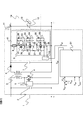
- FIG. 1 is a diagram showing a basic configuration of a power conversion device 11 according to a first embodiment of the present invention.
- the power conversion device 11 shown in FIG. 1 converts a DC voltage input from the DC power supply 1 into a high DC voltage and outputs it to a load 14.
- the power converter 11 includes an input side smoothing capacitor 2, a step-up transformer 3, an AC switching element 4, an AC switching element drive circuit 5, a rectifier diode 6, an output side smoothing capacitor 7, a discharge resistor 8, a discharge switch 9, and a discharge switch drive circuit. 10 and a discharge control unit 51.
- the load 14 is applied with a high DC voltage by the power converter 11, and has a capacitance component 12 and a resistance component 13.
- the load 14 is, for example, ERF or dielectric elastomer.
- the difference value Verr obtained by subtracting the output voltage Vout of the power converter 11 from the predetermined target voltage Vref is input to the discharge controller 51.
- the discharge controller 51 outputs a control signal Vg1 to the AC switching element drive circuit 5 and a control signal Vg2 to the discharge switch drive circuit 10 based on the difference value Verr.
- the AC switching element drive circuit 5 drives the AC switching element 4 according to the control signal Vg1.
- the discharge switch drive circuit 10 drives the discharge switch 9 according to the control signal Vg2.
- the discharge control unit 51 switches the output of the control signals Vg1 and Vg2 so that the power conversion device 11 performs the boosting operation or the discharging operation based on the difference value Verr.
- the discharge controller 51 outputs the control signal Vg1 so that the AC switching element 4 repeats the on state and the off state at high speed, and outputs the control signal Vg2 so that the discharge switch 9 is turned off.
- the input voltage from the DC power source 1 is converted into a high-frequency AC voltage (rectangular wave voltage) by the on / off operation of the AC switching element 4.
- This AC voltage is boosted by the step-up transformer 3 and then converted to a DC voltage by the rectifier diode 6.
- a high output voltage Vout is output from the power converter 11 to the load 14.
- the discharge control unit 51 outputs the control signal Vg1 so that the AC switching element 4 is turned off, and the control signal Vg2 so that the discharge switch 9 is turned on. Output.
- the power converter 11 stops the step-up operation.
- the discharge resistor 8 is energized, and the electric charge accumulated in the capacitive component 12 of the load 14 and the output side smoothing capacitor 7 is discharged by the discharge resistor 8.
- the resistance value of the discharge resistor 8 is smaller than the resistance value of the resistance component 13 of the load 14 so that the discharge resistance 8 can be efficiently discharged.
- the discharge control unit 51 controls the AC switching element 4 and the discharge switch 9 so that the output voltage Vout becomes the target voltage Vref based on the difference value Verr between the target voltage Vref and the output voltage Vout. can do.
- the discharge switch 9 can be constituted by a single high voltage switch. However, since the high voltage switch is expensive, the discharge switch 9 is expensive. Therefore, as will be described below, the discharge switch 9 is preferably configured by a plurality of low-voltage or medium-voltage semiconductor switching elements.
- FIG. 2 is a diagram illustrating a configuration example of the discharge switch 9 in the power conversion device 11.
- the discharge switch 9 is configured by connecting low-voltage or medium-voltage semiconductor switching elements 21 to 23 in series. In this way, since the discharge switch 9 is configured by using the relatively inexpensive low withstand voltage or medium withstand voltage semiconductor switching elements 21 to 23, it is not necessary to use a high withstand voltage switch. it can.
- n-type MOSFETs are used for the semiconductor switches 21 to 23, respectively.
- a snubber circuit / MOSFET gate charging circuit is connected between the drain terminal and the source terminal to suppress a transient voltage imbalance when the semiconductor switches are turned on and off.
- the gate charging circuit of the snubber circuit MOSFET is composed of gate charging resistors 24 to 26, voltage dividing capacitors 27 to 29, charging diodes 30 to 32, and voltage dividing resistors 33 to 35, respectively.
- Zener diodes 36 to 38 are connected between the gate terminals and source terminals of the semiconductor switches 21 to 23, respectively, and the gate charging circuits of the snubber circuit MOSFETs of the semiconductor switches 22 and 23 are Zener diodes 39 and 40, respectively. Are connected to the gate terminals of the semiconductor switches 21 and 22, respectively. As a result, the necessary gate voltages are output from the discharge switch driving circuit 10 to the gate terminals of the semiconductor switches 21 to 23, respectively.
- the discharge switch 9 when the discharge switch 9 is configured by connecting a plurality of semiconductor switching elements 21 to 23 in series, it is necessary to connect voltage dividing capacitors 27 to 29 in parallel with each semiconductor switching element. However, when the voltage dividing capacitors 27 to 29 are connected in this way, the total voltage of the voltage dividing capacitors 27 to 29 becomes the output voltage Vout of the power converter 11 even if all the semiconductor switching elements 21 to 23 are turned off. Since the charging of the voltage dividing capacitors 27 to 29 is continued, the current continues to flow through the discharge switch 9, and the turn-off of the discharge switch 9 is not completed. As a result, an additional turn-off time occurs after the semiconductor switching elements 21 to 23 are turned off in the discharge switch 9, and the high voltage application to the discharge resistor 8 is continued.
- the turn-off time of the discharge switch 9 generated by the voltage dividing capacitors 27 to 29 becomes a dead time that cannot be shifted to the next step-up operation, and becomes a factor that decreases the responsiveness of the power converter 11.
- the turn-off time of the discharge switch 9 is determined according to the charging time constant of the voltage dividing capacitors 27-29.
- the charging time constants of the voltage dividing capacitors 27 to 29 include the capacitance values of the capacitance components 12 of the voltage dividing capacitors 27 to 29, the output side smoothing capacitor 7 and the load 14, the discharge resistors 8, the gate charging resistors 24 to 26 and the load 14. The value is determined by the resistance value of the resistance component 13 or the like.
- FIG. 3 is a diagram for explaining the problems of the prior art in the configuration of the discharge switch 9 shown in FIG.
- FIG. 3 shows the voltage change of the load 14 and the discharge resistor 8 when the control of the discharge switch 9 according to the prior art is performed.
- the discharge switch 9 is turned on at time ton to start the discharge operation of the power converter 11 and reduce the voltage of the load 14 from the pre-discharge voltage Vini to the target voltage Vref.
- the state of the voltage change of the load 14 and the discharge resistor 8 when the discharge switch 9 is turned off at the time toff when the voltage of the load 14 reaches the target voltage Vref is shown.
- the electric charge accumulated in the capacitive component 12 of the load 14 is discharged by the discharging operation of the power converter 11, thereby causing the voltage of the load 14 to be discharged. Decreases as shown in the graph 61.
- the discharge switch 9 is turned off at time toff, high voltage application to the discharge resistor 8 is continued during the turn-off time t2 of the discharge switch 9, and the voltage of the discharge resistor 8 decreases as shown in the graph 62. . Therefore, the power conversion device 11 cannot move to the next boosting operation until the total time t1 + t2 of the time t1 and the time t2 has elapsed.
- a predetermined threshold voltage larger than the target voltage Vref is set for the output voltage Vout. To do. Then, when the output voltage Vout falls below this threshold voltage, the discharge switch 9 is controlled to turn off the discharge switch 9 and cut off the energization of the discharge resistor 8. Further, at this time, the above threshold voltage is corrected in consideration of the temperature dependence of the load 14. Therefore, as shown in FIG. 2, the target voltage Vref and the temperature Tload of the load 14 are input to the discharge control unit 51.
- the temperature Tload of the load 14 can be detected by, for example, a temperature sensor using a thermocouple or other means.
- FIG. 4 is a diagram for explaining the principle of the method for controlling the discharge switch 9 by the power conversion device 11 of the present embodiment.
- the threshold voltage Vth higher than the target voltage Vref is set in the power converter 11, and the state of the voltage change of the load 14 and the discharge resistor 8 when the discharge switch 9 is controlled using this threshold voltage Vth. Is shown.
- the discharge operation of the power converter 11 is started and the voltage of the load 14 is decreased from the pre-discharge voltage Vini toward the target voltage Vref.
- the state of the voltage change of the load 14 and the discharge resistor 8 when the discharge switch 9 is turned off at time toff when the voltage of the load 14 reaches a threshold voltage Vth higher than the target voltage Vref is shown.
- FIG. 5 is a diagram for explaining the principle of the threshold voltage correction method performed by the power conversion apparatus 11 according to this embodiment.
- FIG. 5 shows a state in which the slope of the voltage change of the load 14 due to the discharging operation of the power converter 11 changes according to the temperature.
- the slope of the voltage change of the load 14 during discharge changes depending on the temperature of the load 14.
- the load 14 is ERF
- the voltage of the load 14 decreases as shown in the graph 63 due to the discharging operation of the power converter 11 at room temperature.
- the temperature is high
- the product of the capacitance component 12 and the resistance component 13 of the load 14 changes to a value smaller than that at room temperature, so the charging time constants of the voltage dividing capacitors 27 to 29 are small.
- the gradient of the voltage change of the load 14 increases, and the voltage of the load 14 decreases as shown in the graph 64.
- the threshold voltage for turning off the discharge switch 9 is changed in accordance with the slope change of the voltage change of the load 14 due to the temperature as described above. Specifically, when the temperature of the load 14 is high, the threshold voltage for turning off the discharge switch 9 is increased, for example, to change from the threshold voltage Vth1 at normal temperature to the threshold voltage Vth2 at high temperature. On the other hand, when the temperature of the load 14 is low, the threshold voltage at which the discharge switch 9 is turned off is decreased, for example, changed from the threshold voltage Vth1 at normal temperature to the threshold voltage Vth3 at low temperature. Accordingly, the threshold voltage for turning off the discharge switch 9 can be appropriately corrected in consideration of the temperature dependence of the load 14. As a result, in any case, the turn-off time t2 of the discharge switch 9 that occurs after the discharge switch 9 is turned off can be made comparable.
- the correction of the threshold voltage according to the temperature of the load 14 as described above is applicable not only when the load 14 is ERF but also when other materials such as a dielectric elastomer are used. It is considered that the same effect can be obtained if high voltage application is necessary and the capacitance value and the resistance value are temperature-dependent.
- FIG. 6 is a diagram showing the characteristics of the hysteresis comparator in the discharge controller 51.
- the discharge control unit 51 has a hysteresis comparator having characteristics as shown in FIG. 6 in order to perform on / off control of the discharge switch 9 in accordance with the temperature of the load 14.
- 6A shows the characteristics of the hysteresis comparator when the temperature of the load 14 is normal
- FIG. 6B shows the characteristics of the hysteresis comparator when the temperature of the load 14 is high
- FIG. 6C shows the characteristic of the hysteresis comparator. The characteristics of the hysteresis comparator when the temperature is low are shown.
- the discharge controller 51 When the temperature of the load 14 is normal temperature, the discharge controller 51 outputs a control signal Vg2 to the discharge switch drive circuit 10 according to the characteristics of the hysteresis comparator as shown in FIG. That is, when the value of the control signal Vg2 is the low level VL corresponding to the OFF state of the discharge switch 9, the discharge controller 51 determines that the difference value Verr obtained by subtracting the output voltage Vout from the target voltage Vref is a predetermined discharge start threshold Von. If smaller than this, the control signal Vg2 is changed from the low level VL to the high level VH, and the discharge switch 9 is switched to the ON state.
- the discharge controller 51 determines that the difference value Verr obtained by subtracting the output voltage Vout from the target voltage Vref is a predetermined discharge end threshold Voff.
- the control signal Vg2 is changed from the high level VH to the low level VL, and the discharge switch 9 is switched to the OFF state.
- the discharge control unit 51 keeps the discharge start threshold value Von constant without changing it, and corrects the discharge end threshold value Voff according to the temperature of the load 14. Change the characteristics. For example, when the load 14 is ERF and the temperature of the load 14 changes from room temperature to high temperature, the discharge control unit 51 increases the discharge end threshold Voff in the low voltage side, that is, in the negative direction, as shown in FIG. Next, the characteristics of the hysteresis comparator are changed.
- the discharge control unit 51 changes the characteristics of the hysteresis comparator so as to increase the discharge end threshold Voff in the high voltage side, that is, in the positive direction, as shown in (c). Change.
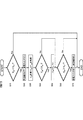
- FIG. 7 is a diagram showing a control flow of the discharge switch 9 in the first embodiment of the present invention. The process shown in this control flow is executed in the discharge control unit 51 when the power converter 11 is performing a boosting operation.
- step S10 the discharge controller 51 determines whether or not the difference value Verr of the output voltage Vout with respect to the input target voltage Vref is smaller than a predetermined discharge start threshold value Von. As a result, if the difference value Verr is smaller than the discharge start threshold value Von, the process proceeds to step S20. If the difference value Verr is equal to or greater than the discharge start threshold value Von, the process shown in the control flow of FIG.
- step S20 the discharge control unit 51 outputs the control signal Vg1 so that the AC switching element 4 is turned off to stop the boosting operation, and outputs the control signal Vg2 so that the discharge switch 9 is turned on. Then, energization of the discharge resistor 8 is started. As a result, the charge accumulated in the capacitive component 12 of the load 14 is discharged, and the voltage of the load 14 decreases.
- step S30 the discharge controller 51 calculates the discharge end threshold Voff based on the input target voltage Vref and the temperature Tload of the load 14.
- the discharge end threshold Voff increases in the negative direction as the temperature Tload of the load 14 increases, and the discharge end threshold Voff increases in the positive direction as the temperature Tload of the load 14 decreases.
- Calculate the end threshold value Voff For example, the discharge end threshold Voff corresponding to the temperature Tload of the load 14 can be calculated in this way by using a table or function stored in advance. Thereby, the threshold voltage Vth with respect to the output voltage Vout can be corrected according to the temperature Tload of the load 14.
- step S40 the discharge controller 51 determines whether or not the value of the discharge end threshold Voff calculated in step S30 is smaller than the discharge start threshold Von.
- the discharge control unit 51 corrects the discharge end threshold Voff to be larger than the discharge start threshold Von in step S50.
- the discharge end threshold value Voff can be corrected.
- the discharge end threshold Voff may be corrected by other methods.
- step S50 the discharge control unit 51 sets a corrected discharge end threshold Voff, and the process proceeds to step S60.
- step S40 when it is determined in step S40 that the discharge end threshold Voff is equal to or greater than the discharge start threshold Von, the discharge control unit 51 sets the discharge end threshold Voff calculated in step S30 without executing step S50. Then, the process proceeds to step S60.
- step S60 the discharge controller 51 determines whether or not the difference value Verr of the output voltage Vout with respect to the input target voltage Vref is smaller than the set discharge end threshold Voff. As a result, if the difference value Verr is larger than the discharge end threshold value Voff, the process proceeds to step S70. If the difference value Verr is equal to or less than the discharge end threshold value Voff, the process shown in the control flow of FIG.
- step S70 the discharge control unit 51 outputs a control signal Vg2 so that the discharge switch 9 is turned off to cut off the energization of the discharge resistor 8, and the control signal so that the AC switching element 4 is repeatedly turned on and off. Outputs Vg1 and starts the boost operation. If step S70 is performed, the discharge control part 51 will complete
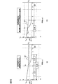
- FIG. 8 shows the voltage change of the load 14 and the discharge resistor 8 when the temperature of the load 14 is normal temperature (50 ° C.).
- (a) shows, as an example of the case where the discharge switch 9 is controlled according to the prior art, and the load 14 when the discharge switch 9 is controlled without setting the threshold voltage Vth described so far. The state of the voltage change of the discharge resistor 8 is shown.
- (b) shows, as an example of controlling the discharge switch 9 according to the present invention, how the voltage of the load 14 and the discharge resistor 8 changes when the threshold voltage Vth is set and the discharge switch 9 is controlled. Is shown. 8, similarly to FIGS. 3 and 4, the voltage change of the load 14 is shown by a graph 61, and the voltage change of the discharge resistor 8 by the turn-off time of the discharge switch 9 is shown by a graph 62.
- the discharge switch 9 is turned off at time toff when the voltage of the load 14 reaches the target voltage Vref. Therefore, as described with reference to FIG. 3, a dead time corresponding to the turn-off time of the discharge switch 9 occurs, and the time from the time ton when the discharge switch 9 is turned on until the turn-off of the discharge switch 9 is completed is 3 .6 [a.u.].
- the threshold voltage Vth when the threshold voltage Vth is set, when the voltage of the load 14 reaches the threshold voltage Vth, as in the case described with reference to FIG.
- the discharge switch 9 is turned off in anticipation of the voltage drop of the load 14 during the turn-off time. Therefore, when the voltage of the load 14 reaches the target voltage Vref, the voltage of the discharge resistor 8 can be reduced by 90% or more from the voltage of the load 14, and the turn-off of the discharge switch 9 can be almost completed.
- the time from when the discharge switch 9 is turned on to when the turn-off of the discharge switch 9 is completed is 2.4 [au]. That is, compared with the case where the threshold voltage Vth is not set, the time from the time ton when the discharge switch 9 is turned on until the turn-off of the discharge switch 9 is completed can be reduced by 30% or more.
- FIG. 9 shows the voltage change of the load 14 and the discharge resistor 8 when the temperature of the load 14 is high (90 ° C.).
- (a) shows an example in which the threshold voltage Vth at high temperature is not corrected, when the discharge switch 9 is controlled using the same threshold voltage Vth as when the temperature of the load 14 is 50 ° C. The state of the voltage change of the load 14 and the discharge resistor 8 is shown.
- (b) shows an example of the case where the threshold voltage Vth at the time of high temperature is corrected, and the load when the discharge switch 9 is controlled using the threshold voltage Vth when the temperature of the load 14 is 90 ° C. 14 and the voltage change of the discharge resistor 8 are shown.
- the voltage change of the load 14 is shown by a graph 61
- the voltage change of the discharge resistor 8 by the turn-off time of the discharge switch 9 is shown by a graph 62.
- the threshold voltage Vth is considered in consideration of the effect that the gradient of the voltage change of the load 14 during discharge increases due to the temperature rise of the load 14. Has increased. Therefore, when the voltage of the load 14 reaches the target voltage Vref, the voltage of the discharge resistor 8 can be reduced by 90% or more from the voltage of the load 14, and the turn-off of the discharge switch 9 can be almost completed. As a result, the time from when the discharge switch 9 is turned on to when the turn-off of the discharge switch 9 is completed is 1.3 [au].
- the time from the time ton when the discharge switch 9 is turned on until the turn-off of the discharge switch 9 is completed can be reduced by about 40%. Further, when the threshold voltage Vth is not corrected, the discharge resistor 8 continues to discharge even though the voltage of the load 14 reaches the target voltage Vref, so that a loss due to overdischarge occurs. On the other hand, when the threshold voltage Vth is corrected, loss due to such overdischarge can also be reduced.
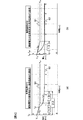
- FIG. 10 shows the voltage change of the load 14 and the discharge resistor 8 when the temperature of the load 14 is low (0 ° C.).
- 10A shows an example in which the threshold voltage Vth at the time of low temperature is not corrected, and the discharge switch 9 is controlled using the same threshold voltage Vth as when the temperature of the load 14 is 50 ° C. The state of the voltage change of the load 14 and the discharge resistor 8 is shown.
- (b) shows a load when the discharge switch 9 is controlled using the threshold voltage Vth when the temperature of the load 14 is 0 ° C., as an example when the threshold voltage Vth at low temperature is corrected. 14 and the voltage change of the discharge resistor 8 are shown.
- the voltage change of the load 14 is shown by a graph 61
- the voltage change of the discharge resistor 8 by the turn-off time of the discharge switch 9 is shown by a graph 62.
- the discharge switch 9 is turned off before the voltage of the load 14 is sufficiently lowered, and the time from when the discharge switch 9 is turned on until the voltage of the load 14 reaches the target voltage Vref is 4.1 [ a.u.].
- the threshold voltage Vth when the threshold voltage Vth is corrected, the threshold voltage Vth is considered in consideration of the effect that the slope of the voltage change of the load 14 at the time of discharge is reduced due to the temperature drop of the load 14. Is decreasing. Therefore, the discharge switch 9 can be turned off when the voltage of the load 14 is sufficiently lowered. As a result, the time from when the discharge switch 9 is turned on until the voltage of the load 14 reaches the target voltage Vref is 3.0 [au]. That is, compared with the case where the threshold voltage Vth is not corrected, the time from when the discharge switch 9 is turned on until the voltage of the load 14 reaches the target voltage Vref can be reduced by about 27%. Furthermore, when the voltage of the load 14 reaches the target voltage Vref, the voltage of the discharge resistor 8 can be reduced by 90% or more from the voltage of the load 14 to almost complete the turn-off of the discharge switch 9.
- the power converter 11 converts a DC input voltage into a DC output voltage Vout and outputs the converted voltage to the load 14.
- the power conversion device 11 discharges the discharge resistor 8 for discharging the electric charge accumulated in the load 14, the discharge switch 9 for switching the energization state of the discharge resistor 8, and the output voltage Vout to a predetermined target voltage Vref.
- the discharge controller 51 controls the discharge switch 9 so as to cut off the energization of the discharge resistor 8 when the output voltage Vout falls below a predetermined threshold voltage Vth that is higher than the target voltage Vref. Further, the discharge control unit 51 corrects the threshold voltage Vth according to the temperature change of the load 14. Since it did in this way, the responsiveness of the power converter device 11 can be improved.
- the discharge control unit 51 corrects the threshold voltage Vth so that the threshold voltage Vth is increased when the temperature of the load 14 is increased and the threshold voltage Vth is decreased when the temperature of the load 14 is decreased. Since it did in this way, the threshold voltage Vth can be correct
- ERF has an advantage of high responsiveness because it can directly control the viscosity of a fluid by an electric signal without having a movable part.
- ERF in order to change the viscosity of ERF, it is necessary to apply an electric field having a high electric field strength of about several hundred to several thousand V / mm. Therefore, when ERF is used for the load 14, the power conversion device 11 of this embodiment needs to apply a high voltage between electrodes filled with ERF with high responsiveness.
- the electrical equivalent circuit of the ERF can be expressed as a parallel circuit of a capacitance component 12 and a resistance component 13 like the load 14 shown in FIGS. Therefore, in the power converter 11, the load 14 can be considered as a capacitor load.
- the power conversion device 11 When increasing the damping force of the ERF damper, the power conversion device 11 is boosted to charge the capacitive component 12 to a voltage corresponding to the desired damping force.
- the damping force of the ERF damper is decreased, the capacitive component 12 is discharged to a voltage corresponding to a desired damping force by causing the power converter 11 to perform a discharging operation. Thereby, the damping force of the ERF damper can be controlled.
- the discharge resistor 8 having a resistance value smaller than the resistance value of the resistance component 13 is an ERF damper in order to improve the response when the damping force of the ERF damper is reduced.
- the load 14 is connected in parallel.
- simply connecting the discharge resistors 8 in parallel is not preferable because power loss occurs in the discharge resistors 8 other than during discharge, leading to a reduction in efficiency of the power converter 11. Therefore, in the power converter 11, in order to achieve both improvement in response when reducing the damping force of the ERF damper and reduction in power loss due to the discharge resistor 8, a discharge switch 9 is connected in series with the discharge resistor 8. ing.
- the discharge switch 9 is turned on only during the discharge operation, and the capacitance component 12 of the load 14 that is an ERF damper is discharged by the discharge resistor 8.
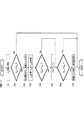
- FIG. 11 is a diagram showing a control flow of the discharge switch 9 in the second embodiment of the present invention.
- the process shown in this control flow is executed in the discharge control unit 51 when the power converter 11 is performing the boosting operation, similarly to the process in the first embodiment shown in the control flow of FIG. .
- the same step numbers are used for the processes having the same contents as in FIG. 7.
- step S1 the discharge control unit 51 calculates a discharge start threshold Von based on the difference value Verr of the output voltage Vout with respect to the input target voltage Vref.
- the discharge start threshold value Von becomes smaller as the difference value Verr obtained by subtracting the output voltage Vout from the target voltage Vref is smaller, that is, as the difference between the target voltage Vref and the output voltage Vout is larger.
- the discharge control unit 51 updates the discharge start threshold value Von based on the calculation result, and the process proceeds to step S10.
- the process after step S10 is the same as FIG. 7, description is abbreviate
- the discharge switch 9 is turned on / off when the difference value Verr is smaller than the discharge end threshold Voff and larger than the discharge start threshold Von. Repeated chattering occurs. Therefore, in the processing flow of FIG. 11, the discharge end threshold value Voff is always limited to be larger than the discharge start threshold value Von by the processing of steps S40 and S50, so that the above chattering does not occur.
- the discharge controller 51 determines that the difference value Verr obtained by subtracting the output voltage Vout from the target voltage Vref is smaller than the predetermined discharge start threshold Von (step S10). : Yes), the discharge switch 9 is controlled so as to start energization of the discharge resistor 8 (step S20). Further, the discharge control unit 51 updates the discharge start threshold value Von so that the discharge start threshold value Von becomes smaller as the difference value Verr obtained by subtracting the output voltage Vout from the target voltage Vref becomes smaller (step S1). Since it did in this way, the setting range of the discharge end threshold value Voff can be expanded without narrowing the operating range of the discharge switch 9, and the effect of the invention can be improved.
- the threshold voltage Vth is corrected based on the detection result.
- the threshold voltage Vth is corrected based on the product of the resistance value and the capacitance value of the load 14.
- FIG. 12 is a diagram showing a configuration of the power conversion device 11 according to the third embodiment of the present invention.
- the power conversion device 11 illustrated in FIG. 12 has the same configuration as the power conversion device 11 according to the first embodiment illustrated in FIG. 2, but some of the information input to the discharge control unit 51 is Is different. That is, in the first embodiment, the temperature Tload of the load 14 is input to the discharge control unit 51, but in this embodiment, the output voltage Vout and the output current Iout of the power converter 11 are discharged instead of the temperature Tload. It is input to the control unit 51.
- the discharge controller 51 calculates the value of the discharge end threshold Voff using the input output voltage Vout and output current Iout. Specifically, based on the output voltage Vout and the output current Iout, the capacitance value of the capacitance component 12 and the resistance value of the resistance component 13 in the load 14 are obtained, and the product of these is calculated. Then, based on the calculated product and the target voltage Vref, the discharge end threshold Voff increases in the negative direction as the product decreases, and the discharge end threshold Voff increases in the positive direction as the product increases. Calculate the value of Voff. For example, the discharge end threshold value Voff corresponding to the product of the capacitance value and the resistance value of the load 14 can be calculated in this way by using a table or function stored in advance.
- the threshold voltage Vth can be increased.
- the threshold voltage Vth can be reduced. Therefore, similarly to the first embodiment, even when the capacitance component 12 and the resistance component 13 of the load 14 have temperature dependence, the threshold voltage for turning off the discharge switch 9 can be appropriately corrected. Furthermore, it is possible to cope with the aging of the load 14.
- the temperature Tload of the load 14 can be estimated based on these temperature characteristics acquired in advance. By using the temperature Tload of the load 14 thus estimated, it is possible to perform the same control as in the first embodiment without a temperature detection means such as a temperature sensor.
- the discharge control unit 51 can calculate the resistance value of the resistance component 13 in the load 14 from the ratio between the output voltage Vout of the power conversion device 11 and the output current Iout flowing from the power conversion device 11 to the load 14. it can.
- the resistance value of the resistance component 13 in the load 14 can be calculated from the conductivity or resistivity of the load 14 and the length and cross-sectional area of the current path in the load 14.
- the discharge control unit 51 can calculate the capacitance value of the capacitance component 12 in the load 14 from the ratio between the charge time constant or discharge time constant of the load 14 and the resistance value of the resistance component 13 in the load 14. it can.
- the capacitance component 12 in the load 14 is calculated from the dielectric constant or relative dielectric constant of the load 14, the distance between the electrodes in the pair of electrodes, and the opposed area. The capacitance value of can also be calculated.
- the discharge control unit 51 may obtain the output voltage Vout and the output current Iout of the power converter 11 by calculation. For example, when the load 14 has a pair of electrodes opposed to each other as described above, the output voltage Vout can be calculated from the distance between the electrodes in the pair of electrodes and the electric field strength. Further, the output current Iout can be calculated from the current density and the cross-sectional area in the current path in the load 14.
- the discharge control unit 51 corrects the threshold voltage Vth according to a change in the product of the capacitance value and the resistance value of the load 14. That is, when the product of the capacitance value and resistance value of the load 14 decreases, the threshold voltage Vth is increased, and when the product of the capacitance value and resistance value of the load 14 increases, the threshold voltage Vth is decreased. The threshold voltage Vth is corrected. Since it did in this way, the threshold voltage Vth can be appropriately corrected according to the change in the slope of the voltage change of the load 14 during discharge due to temperature change or aging change. Therefore, similarly to the first embodiment, the responsiveness of the power converter 11 can be improved.
Landscapes
- Engineering & Computer Science (AREA)
- General Engineering & Computer Science (AREA)
- Power Engineering (AREA)
- Mechanical Engineering (AREA)
- Physics & Mathematics (AREA)
- Electromagnetism (AREA)
- Dc-Dc Converters (AREA)
- Inverter Devices (AREA)
Abstract
直流の入力電圧を直流の出力電圧に変換して負荷に出力する電力変換装置は、前記負荷に蓄積された電荷を放電するための放電抵抗と、前記放電抵抗の通電状態を切り替える放電スイッチと、前記出力電圧が所定の目標電圧となるように前記放電スイッチを制御する放電制御部と、を備え、前記放電制御部は、前記出力電圧が前記目標電圧よりも大きい所定の閾値電圧を下回った場合に、前記放電抵抗の通電を遮断するように前記放電スイッチを制御し、前記放電制御部は、前記負荷の温度変化に応じて前記閾値電圧を補正する。
Description
本発明は、電力変換装置に関する。
電気粘性流体(Electro-Rheological Fluid、以下ERF)は、外部から電場を印加することでその粘性を変化させることができる流体である。ERFは、可動部を有さずに電気信号で流体の粘性を直接制御できるため、応答性が高いという利点がある。車両におけるERFの応用例としては、衝撃吸収、トルク制御、振動制御などのためにそれぞれ利用される、ERFダンパ、ERFクラッチ、ERFエンジンマウントなどが挙げられる。特許文献1では、ERFを利用したショックアブソーバーに高電圧を印加する電力変換装置において、ERFに蓄えられた電荷を放電するための放電スイッチを備えることで、電力変換装置の応答性を低下させることなく、電力損失の低減を図る方法について開示されている。
特許文献1に開示の技術では、放電スイッチと並列に接続された分圧コンデンサの充電時定数に応じて放電スイッチのターンオフ時間が決定される。このターンオフ時間による無駄時間が原因となり、電力変換装置の応答性が低下するという課題がある。
本発明の第1の態様による電力変換装置は、直流の入力電圧を直流の出力電圧に変換して負荷に出力するものであって、前記負荷に蓄積された電荷を放電するための放電抵抗と、前記放電抵抗の通電状態を切り替える放電スイッチと、前記出力電圧が所定の目標電圧となるように前記放電スイッチを制御する放電制御部と、を備え、前記放電制御部は、前記出力電圧が前記目標電圧よりも大きい所定の閾値電圧を下回った場合に、前記放電抵抗の通電を遮断するように前記放電スイッチを制御し、前記放電制御部は、前記負荷の温度変化に応じて前記閾値電圧を補正する。
本発明の第2の態様による電力変換装置は、直流の入力電圧を直流の出力電圧に変換して負荷に出力するものであって、前記負荷に蓄積された電荷を放電するための放電抵抗と、前記放電抵抗の通電状態を切り替える放電スイッチと、前記出力電圧が所定の目標電圧となるように前記放電スイッチを制御する放電制御部と、を備え、前記放電制御部は、前記出力電圧が前記目標電圧よりも大きい所定の閾値電圧を下回った場合に、前記放電抵抗の通電を遮断するように前記放電スイッチを制御し、前記放電制御部は、前記負荷の静電容量値と抵抗値の積の変化に応じて前記閾値電圧を補正する。
本発明の第2の態様による電力変換装置は、直流の入力電圧を直流の出力電圧に変換して負荷に出力するものであって、前記負荷に蓄積された電荷を放電するための放電抵抗と、前記放電抵抗の通電状態を切り替える放電スイッチと、前記出力電圧が所定の目標電圧となるように前記放電スイッチを制御する放電制御部と、を備え、前記放電制御部は、前記出力電圧が前記目標電圧よりも大きい所定の閾値電圧を下回った場合に、前記放電抵抗の通電を遮断するように前記放電スイッチを制御し、前記放電制御部は、前記負荷の静電容量値と抵抗値の積の変化に応じて前記閾値電圧を補正する。
本発明によれば、電力変換装置の応答性を向上できる。
以下、本発明の実施形態を図面とともに説明する。なお、以下の実施形態は本発明の一形態を示すものであり、本発明は要旨を逸脱しない限り、他の形態を含むものである。
(第1の実施形態)
まず、本発明の第1の実施形態について説明する。第1の実施形態では、図1~図10を用いて、本発明の一実施形態を説明する。
まず、本発明の第1の実施形態について説明する。第1の実施形態では、図1~図10を用いて、本発明の一実施形態を説明する。
図1は、本発明の第1の実施形態に係る電力変換装置11の基本構成を示す図である。図1に示す電力変換装置11は、直流電源1から入力される直流電圧を高電圧の直流電圧に変換して負荷14に出力するものである。電力変換装置11は、入力側平滑コンデンサ2、昇圧トランス3、交流スイッチング素子4、交流スイッチング素子駆動回路5、整流ダイオード6、出力側平滑コンデンサ7、放電抵抗8、放電スイッチ9、放電スイッチ駆動回路10および放電制御部51を備える。負荷14は、電力変換装置11によって高電圧の直流電圧が印加されるものであり、容量成分12と抵抗成分13を有している。負荷14は、たとえばERFや誘電性エラストマーなどである。
放電制御部51には、所定の目標電圧Vrefから電力変換装置11の出力電圧Voutを引いた差分値Verrが入力される。放電制御部51は、この差分値Verrに基づいて、交流スイッチング素子駆動回路5への制御信号Vg1および放電スイッチ駆動回路10への制御信号Vg2を出力する。交流スイッチング素子駆動回路5は、制御信号Vg1に応じて交流スイッチング素子4を駆動させる。放電スイッチ駆動回路10は、制御信号Vg2に応じて放電スイッチ9を駆動させる。
放電制御部51は、上記差分値Verrに基づいて、電力変換装置11が昇圧動作または放電動作を行うように、制御信号Vg1、Vg2の出力を切り替える。昇圧動作時には、放電制御部51は、交流スイッチング素子4がオン状態とオフ状態とを高速で繰り返すように制御信号Vg1を出力すると共に、放電スイッチ9がオフ状態となるように制御信号Vg2を出力する。このとき、直流電源1からの入力電圧は、交流スイッチング素子4のオンオフ動作によって高周波の交流電圧(矩形波電圧)に変換される。この交流電圧は、昇圧トランス3で昇圧された後、整流ダイオード6によって直流電圧に変換される。その結果、電力変換装置11から負荷14に高電圧の出力電圧Voutが出力される。
一方、電力変換装置11の放電動作時には、放電制御部51は、交流スイッチング素子4がオフ状態となるように制御信号Vg1を出力すると共に、放電スイッチ9がオン状態となるように制御信号Vg2を出力する。このとき、高周波の交流電圧が昇圧トランス3に印加されないため、電力変換装置11において昇圧動作が停止される。また、放電抵抗8が通電され、負荷14の容量成分12や出力側平滑コンデンサ7に蓄積された電荷が放電抵抗8により放電される。なお、放電抵抗8での放電が効率的に行われるように、放電抵抗8の抵抗値は負荷14の抵抗成分13の抵抗値よりも小さいことが好ましい。
以上説明したような動作により、放電制御部51は、目標電圧Vrefと出力電圧Voutの差分値Verrに基づいて、出力電圧Voutが目標電圧Vrefとなるように交流スイッチング素子4および放電スイッチ9を制御することができる。
次に、放電スイッチ9について説明する。放電スイッチ9は、1つの高耐圧スイッチで構成することもできるが、このようにすると高耐圧スイッチが高価なため、放電スイッチ9が高コスト化してしまう。そこで、以下で説明するように、放電スイッチ9は、複数の低耐圧もしくは中耐圧の半導体スイッチング素子により構成することが好ましい。
図2は、電力変換装置11における放電スイッチ9の構成例を示す図である。図2の例では、低耐圧もしくは中耐圧の半導体スイッチング素子21~23が直列接続されることで放電スイッチ9が構成されている。このように、比較的安価な低耐圧もしくは中耐圧の半導体スイッチング素子21~23を使用して放電スイッチ9を構成することで、高耐圧スイッチを用いる必要がないため、放電スイッチ9を低コスト化できる。
図2において、半導体スイッチ21~23には、それぞれn型MOSFETが用いられている。半導体スイッチ21~23において、ドレイン端子とソース端子の間には、各半導体スイッチ間のオンオフ時の過渡的な電圧不平衡を抑制するためのスナバ回路兼MOSFETのゲート充電回路がそれぞれ接続されている。このスナバ回路MOSFETのゲート充電回路は、ゲート充電抵抗24~26と、分圧コンデンサ27~29と、充電ダイオード30~32と、分圧抵抗33~35とによりそれぞれ構成されている。また、半導体スイッチ21~23のゲート端子とソース端子の間には、ツェナーダイオード36~38がそれぞれ接続されており、半導体スイッチ22、23のスナバ回路MOSFETのゲート充電回路は、ツェナーダイオード39、40を介して、半導体スイッチ21、22のゲート端子にそれぞれ接続されている。これにより、放電スイッチ駆動回路10から半導体スイッチ21~23の各ゲート端子に必要なゲート電圧がそれぞれ出力される。
上記のように、複数の半導体スイッチング素子21~23を直列接続して放電スイッチ9を構成する場合には、各半導体スイッチング素子と並列に分圧コンデンサ27~29を接続する必要がある。しかし、このように分圧コンデンサ27~29を接続すると、半導体スイッチング素子21~23が全てオフとなっても、分圧コンデンサ27~29の合計電圧が電力変換装置11の出力電圧Voutとなるまでは、分圧コンデンサ27~29への充電が継続されて放電スイッチ9に電流が流れ続け、放電スイッチ9のターンオフが完了しない。その結果、放電スイッチ9において半導体スイッチング素子21~23をオフした後に追加のターンオフ時間が生じ、放電抵抗8への高電圧印加が継続される。このターンオフ時間中は、電力変換装置11の出力側が低インピーダンス状態となり、電力変換装置11が昇圧動作を行うと過電流になる恐れがあるため、次の昇圧動作に移れない。このように、従来技術では、分圧コンデンサ27~29によって生じる放電スイッチ9のターンオフ時間は、次の昇圧動作に移れない無駄時間となり、電力変換装置11の応答性を低下させる要因となる。
なお、放電スイッチ9のターンオフ時間は、分圧コンデンサ27~29の充電時定数に応じて決定される。分圧コンデンサ27~29の充電時定数は、分圧コンデンサ27~29、出力側平滑コンデンサ7および負荷14の容量成分12の容量値や、放電抵抗8、ゲート充電抵抗24~26および負荷14の抵抗成分13の抵抗値等によって決まる値である。
図3は、図2に示した放電スイッチ9の構成における従来技術の課題を説明するための図である。図3では、従来技術による放電スイッチ9の制御を行った場合の負荷14と放電抵抗8の電圧変化の様子を示している。具体的には、図3では、時刻tonにおいて放電スイッチ9をオンすることで、電力変換装置11の放電動作を開始して負荷14の電圧を放電前電圧Viniから目標電圧Vrefまで低下させた後、負荷14の電圧が目標電圧Vrefに到達した時刻toffにおいて放電スイッチ9をオフしたときの負荷14と放電抵抗8の電圧変化の様子を示している。
図3に示すように、時刻tonから時刻toffまでの時間t1の間は、電力変換装置11の放電動作によって負荷14の容量成分12に蓄積された電荷が放電されることで、負荷14の電圧がグラフ61に示すように低下していく。時刻toffで放電スイッチ9をオフした後、放電スイッチ9のターンオフ時間t2の間は、放電抵抗8への高電圧印加が継続されており、放電抵抗8の電圧はグラフ62に示すように低下する。したがって、時間t1と時間t2の合計時間t1+t2が経過するまで、電力変換装置11は次の昇圧動作に移ることができない。
そこで、本実施形態の電力変換装置11では、以上説明したような放電スイッチ9のターンオフ時間による無駄時間を低減するために、出力電圧Voutに対して目標電圧Vrefよりも大きい所定の閾値電圧を設定する。そして、出力電圧Voutがこの閾値電圧を下回った場合に、放電スイッチ9をオフして放電抵抗8の通電を遮断するように放電スイッチ9を制御する。さらにこのとき、負荷14の温度依存性を考慮して、上記の閾値電圧を補正する。そのため、図2に示すように、放電制御部51には、目標電圧Vrefや、負荷14の温度Tloadが入力される。負荷14の温度Tloadは、たとえば熱電対等を用いた温度センサや、他の手段により検出することができる。
図4は、本実施形態の電力変換装置11による放電スイッチ9の制御方法の原理を説明するための図である。図4では、電力変換装置11において目標電圧Vrefよりも高い閾値電圧Vthを設定し、この閾値電圧Vthを用いて放電スイッチ9の制御を行った場合の負荷14と放電抵抗8の電圧変化の様子を示している。具体的には、図4では、時刻tonにおいて放電スイッチ9をオンすることで、電力変換装置11の放電動作を開始して負荷14の電圧を放電前電圧Viniから目標電圧Vrefに向かって低下させ、負荷14の電圧が目標電圧Vrefよりも高い閾値電圧Vthに到達した時刻toffにおいて放電スイッチ9をオフしたときの負荷14と放電抵抗8の電圧変化の様子を示している。
図4では、負荷14の電圧が閾値電圧Vthに到達したときに、その後の放電スイッチ9のターンオフ時間t2における負荷14の電圧低下量を見込んで、放電スイッチ9をオフしている。そのため、図3に示した従来技術による制御方法と比べて、時刻tonから時刻toffまでの時間t1を短縮できるため、電力変換装置11において次の昇圧動作までの無駄時間を低減することができる。
図5は、本実施形態の電力変換装置11による閾値電圧の補正方法の原理を説明するための図である。図5では、電力変換装置11の放電動作による負荷14の電圧変化の傾きが温度に応じて変化する様子を示している。
負荷14の容量成分12や抵抗成分13に温度依存性がある場合、図5に示すように、負荷14の温度によって放電時の負荷14の電圧変化の傾きが変化する。たとえば、負荷14がERFである場合、常温時には電力変換装置11の放電動作により、負荷14の電圧がグラフ63に示すように低下していく。これに対して、高温時には、負荷14の容量成分12と抵抗成分13の積が常温時よりも小さな値に変化するため、分圧コンデンサ27~29の充電時定数が小さくなる。その結果、負荷14の電圧変化の傾きが大きくなり、負荷14の電圧がグラフ64に示すように低下していく。一方、低温時には、負荷14の容量成分12と抵抗成分13の積が常温時よりも大きな値に変化するため、分圧コンデンサ27~29の充電時定数が大きくなる。その結果、負荷14の電圧変化の傾きが小さくなり、負荷14の電圧がグラフ65に示すように低下していく。
そこで、本実施形態の電力変換装置11では、上記のような温度による負荷14の電圧変化の傾き変化に応じて、放電スイッチ9をオフする閾値電圧を変化させる。具体的には、負荷14の温度が高いときには、放電スイッチ9をオフする閾値電圧を増加させて、たとえば常温時の閾値電圧Vth1から高温時の閾値電圧Vth2に変化させる。一方、負荷14の温度が低いときには、放電スイッチ9をオフする閾値電圧を減少させて、たとえば常温時の閾値電圧Vth1から低温時の閾値電圧Vth3に変化させる。これにより、負荷14の温度依存性を考慮して、放電スイッチ9をオフする閾値電圧を適切に補正できる。その結果、いずれの場合にも、放電スイッチ9をオフした後に生じる放電スイッチ9のターンオフ時間t2を同程度とすることができる。
なお、以上説明したような負荷14の温度に応じた閾値電圧の補正は、負荷14がERFである場合だけでなく、他の材料、たとえば誘電性エラストマーなどの場合にも適用可能である。高電圧印加が必要であり、かつ静電容量値や抵抗値に温度依存性があるものであれば、同様の効果が得られると考えられる。
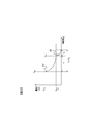
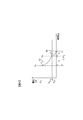
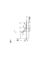
図6は、放電制御部51内のヒステリシスコンパレータの特性を示す図である。放電制御部51は、負荷14の温度に応じて放電スイッチ9のオンオフ制御を行うために、図6に示すような特性のヒステリシスコンパレータを有している。図6において、(a)は負荷14の温度が常温であるときのヒステリシスコンパレータの特性を、(b)は負荷14の温度が高温であるときのヒステリシスコンパレータの特性を、(c)は負荷14の温度が低温であるときのヒステリシスコンパレータの特性を、それぞれ示している。
負荷14の温度が常温である場合に、放電制御部51は、図6(a)に示すようなヒステリシスコンパレータの特性に応じて、放電スイッチ駆動回路10への制御信号Vg2を出力する。すなわち、制御信号Vg2の値が放電スイッチ9のオフ状態に対応するローレベルVLであるときには、放電制御部51は、目標電圧Vrefから出力電圧Voutを引いた差分値Verrが所定の放電開始閾値Vonよりも小さくなると、制御信号Vg2をローレベルVLからハイレベルVHに変化させて、放電スイッチ9をオン状態に切り替える。一方、制御信号Vg2の値が放電スイッチ9のオン状態に対応するハイレベルVHであるときには、放電制御部51は、目標電圧Vrefから出力電圧Voutを引いた差分値Verrが所定の放電終了閾値Voff(Von<Voff)よりも大きくなると、制御信号Vg2をハイレベルVHからローレベルVLに変化させて、放電スイッチ9をオフ状態に切り替える。
負荷14の温度が常温から変化すると、放電制御部51は、放電開始閾値Vonを変化させずに一定としたままで、放電終了閾値Voffを負荷14の温度に応じて補正するように、ヒステリシスコンパレータの特性を変化させる。たとえば負荷14がERFの場合に、負荷14の温度が常温から高温に変化すると、放電制御部51は、(b)に示すように放電終了閾値Voffを低電圧側、すなわち負方向に増加させるように、ヒステリシスコンパレータの特性を変化させる。一方、負荷14の温度が常温から低温に変化すると、放電制御部51は、(c)に示すように放電終了閾値Voffを高電圧側、すなわち正方向に増加させるように、ヒステリシスコンパレータの特性を変化させる。
図7は、本発明の第1の実施形態における放電スイッチ9の制御フローを示す図である。この制御フローに示す処理は、電力変換装置11において昇圧動作が行われているときに、放電制御部51において実行される。
ステップS10において、放電制御部51は、入力された目標電圧Vrefに対する出力電圧Voutの差分値Verrが所定の放電開始閾値Vonよりも小さいか否かを判定する。その結果、差分値Verrが放電開始閾値Vonよりも小さければステップS20に処理を進め、差分値Verrが放電開始閾値Von以上であれば図7の制御フローに示す処理を終了する。
ステップS20において、放電制御部51は、交流スイッチング素子4がオフ状態となるように制御信号Vg1を出力して昇圧動作を停止すると共に、放電スイッチ9がオン状態となるように制御信号Vg2を出力して、放電抵抗8への通電を開始する。これにより、負荷14の容量成分12に蓄積された電荷が放電され、負荷14の電圧が低下していく。
ステップS30において、放電制御部51は、入力された目標電圧Vrefおよび負荷14の温度Tloadに基づいて、放電終了閾値Voffを計算する。ここでは前述のように、負荷14の温度Tloadが高温になるほど放電終了閾値Voffが負方向に増加し、負荷14の温度Tloadが低温になるほど放電終了閾値Voffが正方向に増加するように、放電終了閾値Voffの値を計算する。たとえば、予め記憶されたテーブルや関数等を用いることで、このように負荷14の温度Tloadに応じた放電終了閾値Voffを計算できる。これにより、負荷14の温度Tloadに応じて、出力電圧Voutに対する閾値電圧Vthを補正することができる。
ステップS40において、放電制御部51は、ステップS30で計算した放電終了閾値Voffの値が放電開始閾値Vonよりも小さいか否かを判定する。放電終了閾値Voffが放電開始閾値Vonよりも小さい場合、放電制御部51はステップS50において、放電終了閾値Voffが放電開始閾値Vonよりも大きくなるように補正する。ここでは、たとえば放電開始閾値Vonに所定値xを加えたものを放電終了閾値Voffとすることで、放電終了閾値Voffを補正することができる。なお、放電終了閾値Voffを放電開始閾値Vonよりも大きくできるのであれば、これ以外の方法で放電終了閾値Voffの補正を行ってもよい。ステップS50を実行したら、放電制御部51は補正後の放電終了閾値Voffを設定して、処理をステップS60に進める。一方、ステップS40で放電終了閾値Voffが放電開始閾値Von以上であると判定した場合には、放電制御部51はステップS50を実行せずに、ステップS30で計算した放電終了閾値Voffを設定して、処理をステップS60に進める。
ステップS60において、放電制御部51は、入力された目標電圧Vrefに対する出力電圧Voutの差分値Verrが設定した放電終了閾値Voffよりも小さいか否かを判定する。その結果、差分値Verrが放電終了閾値Voffよりも大きければステップS70に処理を進め、差分値Verrが放電終了閾値Voff以下であれば図7の制御フローに示す処理を終了する。
ステップS70において、放電制御部51は、放電スイッチ9がオフ状態となるように制御信号Vg2を出力して放電抵抗8への通電を遮断すると共に、交流スイッチング素子4がオンオフを繰り返すように制御信号Vg1を出力して、昇圧動作を開始させる。ステップS70を実行したら、放電制御部51は図7の制御フローに示す処理を終了する。
次に、図8から図10に示す負荷14と放電抵抗8の電圧変化の例を用いて、本発明の効果について説明する。なお、図8から図10では、負荷14にERFを用いた場合を想定している。
図8は、負荷14の温度が常温(50℃)である場合の負荷14と放電抵抗8の電圧変化の様子を示している。図8において、(a)は従来技術による放電スイッチ9の制御を行った場合の例として、これまでに説明した閾値電圧Vthを設定せずに放電スイッチ9の制御を行った場合の負荷14と放電抵抗8の電圧変化の様子を示している。一方、(b)は本発明による放電スイッチ9の制御を行った場合の例として、閾値電圧Vthを設定して放電スイッチ9の制御を行った場合の負荷14と放電抵抗8の電圧変化の様子を示している。なお、図8では図3、4と同様に、負荷14の電圧変化をグラフ61で示し、放電スイッチ9のターンオフ時間による放電抵抗8の電圧変化をグラフ62で示している。
図8(a)に示すように、閾値電圧Vthを設定しなかった場合は、負荷14の電圧が目標電圧Vrefに到達した時刻toffにおいて放電スイッチ9をオフしている。そのため、図3で説明したのと同様に、放電スイッチ9のターンオフ時間に応じた無駄時間が発生し、放電スイッチ9をオンした時刻tonから放電スイッチ9のターンオフが完了するまでの時間は、3.6[a.u.]となっている。
一方、図8(b)に示すように、閾値電圧Vthを設定した場合は、図4で説明したのと同様に、負荷14の電圧が閾値電圧Vthに到達したときに、その後の放電スイッチ9のターンオフ時間における負荷14の電圧低下量を見込んで、放電スイッチ9をオフしている。そのため、負荷14の電圧が目標電圧Vrefに達した時点で、放電抵抗8の電圧を負荷14の電圧から90%以上低下させ、放電スイッチ9のターンオフを概ね完了することができる。その結果、放電スイッチ9をオンした時刻tonから放電スイッチ9のターンオフが完了するまでの時間は、2.4[a.u.]となっている。すなわち、閾値電圧Vthを設定しなかった場合と比較して、放電スイッチ9をオンした時刻tonから放電スイッチ9のターンオフが完了するまでの時間を30%以上低減することができる。
図9は、負荷14の温度が高温(90℃)である場合の負荷14と放電抵抗8の電圧変化の様子を示している。図9において、(a)は高温時の閾値電圧Vthの補正を行わない場合の例として、負荷14の温度が50℃のときと同じ閾値電圧Vthを用いて放電スイッチ9の制御を行った場合の負荷14と放電抵抗8の電圧変化の様子を示している。一方、(b)は高温時の閾値電圧Vthの補正を行った場合の例として、負荷14の温度が90℃であるときの閾値電圧Vthを用いて放電スイッチ9の制御を行った場合の負荷14と放電抵抗8の電圧変化の様子を示している。なお、図9でも図3、4と同様に、負荷14の電圧変化をグラフ61で示し、放電スイッチ9のターンオフ時間による放電抵抗8の電圧変化をグラフ62で示している。
図9(a)に示すように、閾値電圧Vthを補正しなかった場合は、負荷14の温度上昇によって放電時の負荷14の電圧変化の傾きが大きくなった影響が考慮されていない。そのため、負荷14の電圧が目標電圧Vrefに達した時点でも、1.2[a.u.]の電圧が放電抵抗8に印加されている。したがって、ここから放電抵抗8の電圧が負荷14の電圧から90%以上低下して放電スイッチ9のターンオフを概ね完了するまでに、放電スイッチ9のターンオフ時間に応じた無駄時間として、さらに1.0[a.u.]の時間がかかる。その結果、放電スイッチ9をオンした時刻tonから放電スイッチ9のターンオフが完了するまでの時間は、2.2[a.u.]となっている。
一方、図9(b)に示すように、閾値電圧Vthを補正した場合は、負荷14の温度上昇によって放電時の負荷14の電圧変化の傾きが大きくなった影響を考慮して、閾値電圧Vthが増加している。そのため、負荷14の電圧が目標電圧Vrefに到達した時点で、放電抵抗8の電圧を負荷14の電圧から90%以上低下させ、放電スイッチ9のターンオフを概ね完了することができる。その結果、放電スイッチ9をオンした時刻tonから放電スイッチ9のターンオフが完了するまでの時間は、1.3[a.u.]となっている。すなわち、閾値電圧Vthを補正しなかった場合と比較して、放電スイッチ9をオンした時刻tonから放電スイッチ9のターンオフが完了するまでの時間を40%程度低減することができる。さらに、閾値電圧Vthを補正しなかった場合は、負荷14の電圧が目標電圧Vrefに達したにも関わらず放電抵抗8での放電が継続されるため、過放電による損失が発生する。一方、閾値電圧Vthを補正した場合は、こうした過放電による損失も低減できる。
図10は、負荷14の温度が低温(0℃)である場合の負荷14と放電抵抗8の電圧変化の様子を示している。図10において、(a)は低温時の閾値電圧Vthの補正を行わない場合の例として、負荷14の温度が50℃のときと同じ閾値電圧Vthを用いて放電スイッチ9の制御を行った場合の負荷14と放電抵抗8の電圧変化の様子を示している。一方、(b)は低温時の閾値電圧Vthの補正を行った場合の例として、負荷14の温度が0℃であるときの閾値電圧Vthを用いて放電スイッチ9の制御を行った場合の負荷14と放電抵抗8の電圧変化の様子を示している。なお、図10でも図3、4と同様に、負荷14の電圧変化をグラフ61で示し、放電スイッチ9のターンオフ時間による放電抵抗8の電圧変化をグラフ62で示している。
図10(a)に示すように、閾値電圧Vthを補正しなかった場合は、負荷14の温度低下によって放電時の負荷14の電圧変化の傾きが小さくなった影響が考慮されていない。そのため、負荷14の電圧が十分に低下する前に放電スイッチ9がオフされてしまい、放電スイッチ9をオンした時刻tonから負荷14の電圧が目標電圧Vrefに達するまでの時間は、4.1[a.u.]となっている。
一方、図10(b)に示すように、閾値電圧Vthを補正した場合は、負荷14の温度低下によって放電時の負荷14の電圧変化の傾きが小さくなった影響を考慮して、閾値電圧Vthが減少している。そのため、負荷14の電圧が十分に低下した時点で放電スイッチ9をオフすることができる。その結果、放電スイッチ9をオンした時刻tonから負荷14の電圧が目標電圧Vrefに達するまでの時間は、3.0[a.u.]となっている。すなわち、閾値電圧Vthを補正しなかった場合と比較して、放電スイッチ9をオンした時刻tonから負荷14の電圧が目標電圧Vrefに達するまでの時間を27%程度低減することができる。さらに、負荷14の電圧が目標電圧Vrefに到達した時点で、放電抵抗8の電圧を負荷14の電圧から90%以上低下させ、放電スイッチ9のターンオフを概ね完了することもできる。
以上説明した本発明の第1の実施形態によれば、以下の作用効果を奏する。
(1)電力変換装置11は、直流の入力電圧を直流の出力電圧Voutに変換して負荷14に出力する。電力変換装置11は、負荷14に蓄積された電荷を放電するための放電抵抗8と、放電抵抗8の通電状態を切り替える放電スイッチ9と、出力電圧Voutが所定の目標電圧Vrefとなるように放電スイッチ9を制御する放電制御部51とを備える。放電制御部51は、出力電圧Voutが目標電圧Vrefよりも大きい所定の閾値電圧Vthを下回った場合に、放電抵抗8の通電を遮断するように放電スイッチ9を制御する。また、放電制御部51は、負荷14の温度変化に応じて閾値電圧Vthを補正する。このようにしたので、電力変換装置11の応答性を向上できる。
(2)放電制御部51は、負荷14の温度が上昇したときには閾値電圧Vthを増加させ、負荷14の温度が低下したときには閾値電圧Vthを減少させるように、閾値電圧Vthを補正する。このようにしたので、温度変化による放電時の負荷14の電圧変化の傾きの変化に応じて、閾値電圧Vthを適切に補正することができる。
ここで、負荷14にERFを用いた場合の電力変換装置11の動作について説明する。前述のようにERFは、可動部を有さずに電気信号で流体の粘性を直接制御できるため、応答性が高いという利点がある。しかし、ERFの粘度を変化させるには、数百から数千V/mm程度の高い電界強度の電場を印加する必要がある。そのため、負荷14にERFを用いた場合、本実施形態の電力変換装置11は、ERFが充填された電極間に高電圧を高い応答性で印加する必要がある。たとえば、路面の凹凸に応じてERFの粘度を変化させることで減衰力を制御する自動車用のERFダンパでは、より高い周波数帯の振動を低減するために、負荷14に高電圧を印加する電力変換装置11に対して高い応答性が求められる。また、路面の凹凸に応じて減衰力を一定の範囲内の任意の値に制御するために、出力電圧が一定の範囲内で可変であることも求められる。
ERFの電気的な等価回路は、図1、2に示した負荷14のように、容量成分12と抵抗成分13の並列回路として表すことができる。そのため、電力変換装置11では、負荷14をコンデンサ負荷として考えることができる。ERFダンパの減衰力を増加させる際には、電力変換装置11を昇圧動作させることで、容量成分12を所望の減衰力に応じた電圧にまで充電する。一方、ERFダンパの減衰力を減少させる際には、電力変換装置11を放電動作させることで、容量成分12を所望の減衰力に応じた電圧にまで放電する。これにより、ERFダンパの減衰力を制御することができる。
本実施形態の電力変換装置11では、ERFダンパの減衰力を減少させるときの応答性を向上させるために、抵抗成分13の抵抗値よりも小さい抵抗値を有する放電抵抗8を、ERFダンパである負荷14に並列接続している。しかし、単に放電抵抗8を並列接続しただけでは、放電時以外にも放電抵抗8で電力損失が発生するため、電力変換装置11の効率低下を招いてしまい好ましくない。そこで、電力変換装置11では、ERFダンパの減衰力を減少させるときの応答性向上と、放電抵抗8による電力損失の低減とを両立させるために、放電抵抗8と直列に放電スイッチ9を接続している。そして、放電動作時にのみ放電スイッチ9をオンして、ERFダンパである負荷14の容量成分12を放電抵抗8で放電するようにしている。
(第2の実施形態)
次に、本発明の第2の実施形態について説明する。第2の実施形態では、図11を用いて、本発明の一実施形態を説明する。
次に、本発明の第2の実施形態について説明する。第2の実施形態では、図11を用いて、本発明の一実施形態を説明する。
前述の第1の実施形態では、放電開始閾値Vonを変化させずに一定としたままで、放電終了閾値Voffを負荷14の温度に応じて補正する例を説明した。これに対して、本発明の第2の実施形態では、目標電圧Vrefと出力電圧Voutの差に応じて放電開始閾値Vonを変化させる例を説明する。
図11は、本発明の第2の実施形態における放電スイッチ9の制御フローを示す図である。この制御フローに示す処理は、図7の制御フローで示した第1の実施形態における処理と同様に、電力変換装置11において昇圧動作が行われているときに、放電制御部51において実行される。なお、図11において、図7と同じ内容の処理については、同一のステップ番号としている。
ステップS1において、放電制御部51は、入力された目標電圧Vrefに対する出力電圧Voutの差分値Verrに基づいて、放電開始閾値Vonを計算する。ここでは、目標電圧Vrefから出力電圧Voutを引いた差分値Verrの値が小さいほど、すなわち、目標電圧Vrefと出力電圧Voutの差が大きいほど、放電開始閾値Vonの値が小さくなるように、放電開始閾値Vonを計算する。放電開始閾値Vonを計算できたら、放電制御部51はその計算結果に基づいて放電開始閾値Vonを更新し、処理をステップS10に進める。なお、ステップS10以降の処理については図7と同じであるため、説明を省略する。
ここで、放電終了閾値Voffが放電開始閾値Vonよりも小さいと、差分値Verrが放電終了閾値Voffよりも小さく、かつ放電開始閾値Vonよりも大きい状態となったときに、放電スイッチ9がオンオフを繰り返すチャタリングが発生してしまう。そのため、図11の処理フローでは、ステップS40、S50の処理により、放電終了閾値Voffが必ず放電開始閾値Vonよりも大きくなるように制限して、上記のチャタリングが発生しないようにしている。
以上説明した本発明の第2の実施形態によれば、放電制御部51は、目標電圧Vrefから出力電圧Voutを引いた差分値Verrが所定の放電開始閾値Vonよりも小さくなった場合(ステップS10:Yes)に、放電抵抗8の通電を開始するように放電スイッチ9を制御する(ステップS20)。また、放電制御部51は、目標電圧Vrefから出力電圧Voutを引いた差分値Verrが小さいほど放電開始閾値Vonが小さくなるように、放電開始閾値Vonを更新する(ステップS1)。このようにしたので、放電スイッチ9の動作範囲を狭めることなく、放電終了閾値Voffの設定範囲を拡大し、発明の効果を向上させることができる。すなわち、放電終了閾値Voffの設定範囲を拡大するためには、放電開始閾値Vonを負方向に大きな値に設定する必要があるが、常にこのようにすると放電スイッチ9の動作範囲が狭くなってしまう。そこで、上記のように目標電圧Vrefと出力電圧Voutの差に応じて放電開始閾値Vonを適切な値に更新することで、放電スイッチ9の動作範囲を狭めることなく、放電終了閾値Voffの設定範囲を拡大することができる。その結果、第1の実施形態で説明したような本発明による効果を最大化することが可能となる。
(第3の実施形態)
次に、本発明の第3の実施形態について説明する。第3の実施形態では、図12を用いて、本発明の一実施形態を説明する。
次に、本発明の第3の実施形態について説明する。第3の実施形態では、図12を用いて、本発明の一実施形態を説明する。
前述の第1の実施形態では、負荷14の温度Tloadを検出し、その検出結果に基づいて閾値電圧Vthを補正する例を説明した。これに対して、本発明の第3の実施形態では、負荷14の抵抗値と静電容量値の積に基づいて閾値電圧Vthを補正する例を説明する。
図12は、本発明の第3の実施形態に係る電力変換装置11の構成を示す図である。図12に示す電力変換装置11は、図2に示した第1の実施形態に係る電力変換装置11と同一の構成を有しているが、放電制御部51に入力される情報の一部が異なっている。すなわち、第1の実施形態では、負荷14の温度Tloadが放電制御部51に入力されているが、本実施形態では温度Tloadに代えて、電力変換装置11の出力電圧Voutおよび出力電流Ioutが放電制御部51に入力されている。
本実施形態において、放電制御部51は、入力された出力電圧Voutおよび出力電流Ioutを用いて、放電終了閾値Voffの値を計算する。具体的には、出力電圧Voutおよび出力電流Ioutに基づいて、負荷14における容量成分12の静電容量値および抵抗成分13の抵抗値を求め、これらの積を計算する。そして、計算した積と目標電圧Vrefに基づいて、積が低下するほど放電終了閾値Voffが負方向に増加し、積が上昇するほど放電終了閾値Voffが正方向に増加するように、放電終了閾値Voffの値を計算する。たとえば、予め記憶されたテーブルや関数等を用いることで、このように負荷14の静電容量値と抵抗値の積に応じた放電終了閾値Voffを計算できる。これにより、負荷14の温度上昇により容量成分12の静電容量値および抵抗成分13の抵抗値の積が低下することで、放電時の負荷14の電圧変化の傾きが大きくなったときには、その影響を考慮して、閾値電圧Vthを増加させることができる。一方、負荷14の温度低下により容量成分12の静電容量値および抵抗成分13の抵抗値の積が上昇することで、放電時の負荷14の電圧変化の傾きが小さくなったときには、その影響を考慮して、閾値電圧Vthを減少させることができる。したがって、第1の実施形態と同様に、負荷14の容量成分12や抵抗成分13に温度依存性がある場合でも、放電スイッチ9をオフする閾値電圧を適切に補正できる。さらに、負荷14の経年変化にも対応可能である。
なお、負荷14における容量成分12の静電容量値や抵抗成分13の抵抗値の経年変化が小さければ、出力電圧Voutおよび出力電流Ioutから求めた静電容量値と抵抗値のいずれか少なくとも一方と、事前に取得していたこれらの温度特性とに基づいて、負荷14の温度Tloadを推定することができる。こうして推定した負荷14の温度Tloadを用いることで、温度センサ等の温度検出手段がなくても、第1の実施形態と同様の制御を行うことが可能となる。
ここで、放電制御部51は、電力変換装置11の出力電圧Voutと、電力変換装置11から負荷14に流れる出力電流Ioutとの比から、負荷14における抵抗成分13の抵抗値を計算することができる。あるいは、負荷14の導電率または抵抗率と、負荷14内の電流経路の長さおよび断面積から、負荷14における抵抗成分13の抵抗値を計算することもできる。
また、放電制御部51は、負荷14の充電時定数または放電時定数と、負荷14における抵抗成分13の抵抗値との比から、負荷14における容量成分12の静電容量値を計算することができる。あるいは、負荷14が互いに対向する一対の電極を両端に有する場合には、負荷14の誘電率または比誘電率と、上記一対の電極における電極間の距離および対向面積から、負荷14における容量成分12の静電容量値を計算することもできる。
さらに、放電制御部51は、電力変換装置11の出力電圧Voutや出力電流Ioutを計算により求めてもよい。たとえば、上記のように負荷14が互いに対向する一対の電極を両端に有する場合には、この一対の電極における電極間の距離および電界強度から、出力電圧Voutを計算することができる。また、負荷14内の電流経路における電流密度と断面積から、出力電流Ioutを計算することができる。
以上説明した本発明の第3の実施形態によれば、放電制御部51は、負荷14の静電容量値と抵抗値の積の変化に応じて閾値電圧Vthを補正する。すなわち、負荷14の静電容量値と抵抗値の積が低下したときには閾値電圧Vthを増加させ、負荷14の静電容量値と抵抗値の積が上昇したときには閾値電圧Vthを減少させるように、閾値電圧Vthを補正する。このようにしたので、温度変化や経年変化による放電時の負荷14の電圧変化の傾きの変化に応じて、閾値電圧Vthを適切に補正することができる。したがって、第1の実施形態と同様に、電力変換装置11の応答性を向上できる。
なお、以上説明した実施形態はあくまで一例であり、発明の特徴が損なわれない限り、本発明はこれらの内容に限定されるものではない。また、上記では種々の実施形態を説明したが、本発明はこれらの内容に限定されるものではない。本発明の技術的思想の範囲内で考えられるその他の態様も本発明の範囲内に含まれる。
次の優先権基礎出願の開示内容は引用文としてここに組み込まれる。
日本国特許出願2016年第156624号(2016年8月9日出願)
日本国特許出願2016年第156624号(2016年8月9日出願)
1 直流電源
2 入力側平滑コンデンサ
3 昇圧トランス
4 交流スイッチング素子
5 交流スイッチング素子駆動回路
6 整流ダイオード
7 出力側平滑コンデンサ
8 放電抵抗
9 放電スイッチ
10 放電スイッチ駆動回路
11 電力変換装置
12 容量成分
13 抵抗成分
14 負荷
51 放電制御部
2 入力側平滑コンデンサ
3 昇圧トランス
4 交流スイッチング素子
5 交流スイッチング素子駆動回路
6 整流ダイオード
7 出力側平滑コンデンサ
8 放電抵抗
9 放電スイッチ
10 放電スイッチ駆動回路
11 電力変換装置
12 容量成分
13 抵抗成分
14 負荷
51 放電制御部
Claims (17)
- 直流の入力電圧を直流の出力電圧に変換して負荷に出力する電力変換装置であって、
前記負荷に蓄積された電荷を放電するための放電抵抗と、
前記放電抵抗の通電状態を切り替える放電スイッチと、
前記出力電圧が所定の目標電圧となるように前記放電スイッチを制御する放電制御部と、を備え、
前記放電制御部は、前記出力電圧が前記目標電圧よりも大きい所定の閾値電圧を下回った場合に、前記放電抵抗の通電を遮断するように前記放電スイッチを制御し、
前記放電制御部は、前記負荷の温度変化に応じて前記閾値電圧を補正する電力変換装置。 - 請求項1に記載の電力変換装置において、
前記放電制御部は、前記負荷の温度が上昇したときには前記閾値電圧を増加させ、前記負荷の温度が低下したときには前記閾値電圧を減少させるように、前記閾値電圧を補正する電力変換装置。 - 請求項1または請求項2に記載の電力変換装置において、
前記放電制御部は、前記負荷の静電容量値および抵抗値のいずれか少なくとも一方に基づいて前記負荷の温度を推定する電力変換装置。 - 直流の入力電圧を直流の出力電圧に変換して負荷に出力する電力変換装置であって、
前記負荷に蓄積された電荷を放電するための放電抵抗と、
前記放電抵抗の通電状態を切り替える放電スイッチと、
前記出力電圧が所定の目標電圧となるように前記放電スイッチを制御する放電制御部と、を備え、
前記放電制御部は、前記出力電圧が前記目標電圧よりも大きい所定の閾値電圧を下回った場合に、前記放電抵抗の通電を遮断するように前記放電スイッチを制御し、
前記放電制御部は、前記負荷の静電容量値と抵抗値の積の変化に応じて前記閾値電圧を補正する電力変換装置。 - 請求項4に記載の電力変換装置において、
前記放電制御部は、前記負荷の静電容量値と抵抗値の積が低下したときには前記閾値電圧を増加させ、前記負荷の静電容量値と抵抗値の積が上昇したときには前記閾値電圧を減少させるように、前記閾値電圧を補正する電力変換装置。 - 請求項3から請求項5までのいずれか一項に記載の電力変換装置において、
前記放電制御部は、前記出力電圧と前記負荷に流れる出力電流の比から前記負荷の抵抗値を求める電力変換装置。 - 請求項3から請求項5までのいずれか一項に記載の電力変換装置において、
前記放電制御部は、前記負荷の導電率または抵抗率と、前記負荷内の電流経路の長さおよび断面積とに基づいて、前記負荷の抵抗値を求める電力変換装置。 - 請求項3から請求項7までのいずれか一項に記載の電力変換装置において、
前記放電制御部は、前記負荷の充電時定数または放電時定数と前記負荷の抵抗値の比から前記負荷の静電容量値を求める電力変換装置。 - 請求項3から請求項7までのいずれか一項に記載の電力変換装置において、
前記負荷は互いに対向する一対の電極を両端に有し、
前記放電制御部は、前記負荷の誘電率または比誘電率と、前記一対の電極における電極間の距離および対向面積とに基づいて、前記負荷の静電容量値を求める電力変換装置。 - 請求項1から請求項9までのいずれか一項に記載の電力変換装置において、
前記負荷は互いに対向する一対の電極を両端に有し、
前記放電制御部は、前記一対の電極における電極間の距離および電界強度に基づいて前記出力電圧を求める電力変換装置。 - 請求項6に記載の電力変換装置において、
前記放電制御部は、前記負荷の電流経路における電流密度と断面積に基づいて前記出力電流を求める電力変換装置。 - 請求項1から請求項11までのいずれか一項に記載の電力変換装置において、
前記負荷は電気粘性流体である電力変換装置。 - 請求項1から請求項11までのいずれか一項に記載の電力変換装置において、
前記負荷は誘電性エラストマーである電力変換装置。 - 請求項1から請求項13までのいずれか一項に記載の電力変換装置において、
前記放電スイッチは、複数の半導体スイッチを直列接続して構成されており、
前記複数の半導体スイッチの各々は、コレクタ端子またはドレイン端子と、エミッタ端子またはソース端子とを有しており、
各半導体スイッチの前記コレクタ端子と前記エミッタ端子の間、または前記ドレイン端子と前記ソース端子の間に、コンデンサがそれぞれ接続されている電力変換装置。 - 請求項1から請求項13までのいずれか一項に記載の電力変換装置において、
前記放電スイッチは、複数の半導体スイッチを直列接続して構成されており、
前記複数の半導体スイッチの各々は、ゲート端子と、エミッタ端子またはソース端子とを有しており、
互いに隣接する一対の半導体スイッチにおいて、低電圧側の半導体スイッチの前記エミッタ端子または前記ソース端子と高電圧側の半導体スイッチの前記ゲート端子の間に、コンデンサがそれぞれ接続されている電力変換装置。 - 請求項1から請求項15までのいずれか一項に記載の電力変換装置において、
前記放電制御部は、前記目標電圧から前記出力電圧を引いた値が所定の放電開始閾値よりも小さくなった場合に、前記放電抵抗の通電を開始するように前記放電スイッチを制御し、
前記放電制御部は、前記放電開始閾値を更新する電力変換装置。 - 請求項16に記載の電力変換装置において、
前記放電制御部は、前記目標電圧から前記出力電圧を引いた値が小さいほど前記放電開始閾値が小さくなるように、前記放電開始閾値を更新する電力変換装置。
Priority Applications (3)
| Application Number | Priority Date | Filing Date | Title |
|---|---|---|---|
| CN201780042740.3A CN109478850A (zh) | 2016-08-09 | 2017-05-11 | 电力转换装置 |
| DE112017002936.8T DE112017002936T5 (de) | 2016-08-09 | 2017-05-11 | Leistungsumsetzer |
| US16/319,857 US20190273440A1 (en) | 2016-08-09 | 2017-05-11 | Power Converter |
Applications Claiming Priority (2)
| Application Number | Priority Date | Filing Date | Title |
|---|---|---|---|
| JP2016-156624 | 2016-08-09 | ||
| JP2016156624A JP2018026937A (ja) | 2016-08-09 | 2016-08-09 | 電力変換装置 |
Publications (1)
| Publication Number | Publication Date |
|---|---|
| WO2018029928A1 true WO2018029928A1 (ja) | 2018-02-15 |
Family
ID=61162087
Family Applications (1)
| Application Number | Title | Priority Date | Filing Date |
|---|---|---|---|
| PCT/JP2017/017860 Ceased WO2018029928A1 (ja) | 2016-08-09 | 2017-05-11 | 電力変換装置 |
Country Status (5)
| Country | Link |
|---|---|
| US (1) | US20190273440A1 (ja) |
| JP (1) | JP2018026937A (ja) |
| CN (1) | CN109478850A (ja) |
| DE (1) | DE112017002936T5 (ja) |
| WO (1) | WO2018029928A1 (ja) |
Cited By (2)
| Publication number | Priority date | Publication date | Assignee | Title |
|---|---|---|---|---|
| EP3565074A1 (de) * | 2018-05-04 | 2019-11-06 | Bender GmbH & Co. KG | Ankopplungsschaltung mit schaltender funktion zur ankopplung eines isolationsüberwachungsgerätes an ein ungeerdetes stromversorgungssystem |
| JPWO2019230430A1 (ja) * | 2018-05-28 | 2020-06-18 | 三菱電機株式会社 | 電力変換装置 |
Families Citing this family (3)
| Publication number | Priority date | Publication date | Assignee | Title |
|---|---|---|---|---|
| JP2020051501A (ja) * | 2018-09-26 | 2020-04-02 | 日立オートモティブシステムズ株式会社 | サスペンション制御装置 |
| JP7458015B2 (ja) * | 2019-05-28 | 2024-03-29 | パナソニックIpマネジメント株式会社 | 負荷制御装置、負荷制御方法及びプログラム |
| CN112311215B (zh) * | 2019-08-02 | 2021-10-15 | 台达电子企业管理(上海)有限公司 | 钳位电路和功率模块 |
Citations (2)
| Publication number | Priority date | Publication date | Assignee | Title |
|---|---|---|---|---|
| US20030206421A1 (en) * | 2002-02-05 | 2003-11-06 | Agency For Defense Development | High voltage DC power supplier |
| JP2016063697A (ja) * | 2014-09-19 | 2016-04-25 | 株式会社デンソー | スイッチング素子の故障検出回路 |
Family Cites Families (7)
| Publication number | Priority date | Publication date | Assignee | Title |
|---|---|---|---|---|
| JPH0891031A (ja) | 1994-09-27 | 1996-04-09 | Nissan Motor Co Ltd | 車両用ショックアブソーバー |
| FR2862448B1 (fr) * | 2003-11-14 | 2006-12-29 | St Microelectronics Sa | Generateur de rampe de tension avec un asservissement de pente |
| JP4367374B2 (ja) * | 2005-05-16 | 2009-11-18 | パナソニック株式会社 | 蓄電装置 |
| JP5735825B2 (ja) * | 2011-03-08 | 2015-06-17 | ローム株式会社 | 発光素子駆動用のスイッチング電源の制御回路およびそれらを用いた発光装置および電子機器 |
| JP5942083B2 (ja) * | 2011-12-15 | 2016-06-29 | パナソニックIpマネジメント株式会社 | キャパシタ装置 |
| CN102882253B (zh) * | 2012-09-25 | 2014-11-05 | 常州格力博有限公司 | 智能供电电源及其供电方法 |
| JP6476986B2 (ja) | 2015-02-23 | 2019-03-06 | 日立金属株式会社 | センサ付きケーブル |
-
2016
- 2016-08-09 JP JP2016156624A patent/JP2018026937A/ja not_active Ceased
-
2017
- 2017-05-11 WO PCT/JP2017/017860 patent/WO2018029928A1/ja not_active Ceased
- 2017-05-11 US US16/319,857 patent/US20190273440A1/en not_active Abandoned
- 2017-05-11 DE DE112017002936.8T patent/DE112017002936T5/de not_active Withdrawn
- 2017-05-11 CN CN201780042740.3A patent/CN109478850A/zh active Pending
Patent Citations (2)
| Publication number | Priority date | Publication date | Assignee | Title |
|---|---|---|---|---|
| US20030206421A1 (en) * | 2002-02-05 | 2003-11-06 | Agency For Defense Development | High voltage DC power supplier |
| JP2016063697A (ja) * | 2014-09-19 | 2016-04-25 | 株式会社デンソー | スイッチング素子の故障検出回路 |
Cited By (3)
| Publication number | Priority date | Publication date | Assignee | Title |
|---|---|---|---|---|
| EP3565074A1 (de) * | 2018-05-04 | 2019-11-06 | Bender GmbH & Co. KG | Ankopplungsschaltung mit schaltender funktion zur ankopplung eines isolationsüberwachungsgerätes an ein ungeerdetes stromversorgungssystem |
| US11515701B2 (en) | 2018-05-04 | 2022-11-29 | Bender Gmbh & Co. Kg | Coupling circuit with switching function for coupling an insulation monitoring device to an unearthed power supply system |
| JPWO2019230430A1 (ja) * | 2018-05-28 | 2020-06-18 | 三菱電機株式会社 | 電力変換装置 |
Also Published As
| Publication number | Publication date |
|---|---|
| CN109478850A (zh) | 2019-03-15 |
| US20190273440A1 (en) | 2019-09-05 |
| JP2018026937A (ja) | 2018-02-15 |
| DE112017002936T5 (de) | 2019-03-14 |
Similar Documents
| Publication | Publication Date | Title |
|---|---|---|
| US8704505B2 (en) | Switching power source apparatus | |
| JP4238914B2 (ja) | スイッチング電源回路 | |
| JP2018026937A (ja) | 電力変換装置 | |
| US20150061613A1 (en) | Dc-dc converter and method of controlling dc-dc converter | |
| JP6702010B2 (ja) | スイッチング電源装置 | |
| US10461736B2 (en) | Semiconductor device | |
| JP2021048716A (ja) | スイッチング電源装置 | |
| US20190267895A1 (en) | Dc-dc converter | |
| CN106558979B (zh) | 半导体装置 | |
| JP2008067593A (ja) | 絶縁ゲート型半導体スイッチ素子のゲート駆動回路 | |
| US10491127B2 (en) | Power supply control unit and isolation type switching power supply device | |
| JP6946772B2 (ja) | 電力変換装置 | |
| EP4191857B1 (en) | Adaptive controller for a voltage converter | |
| JP2018121377A (ja) | スイッチング電源装置 | |
| WO2020121727A1 (ja) | ゲート駆動回路 | |
| WO2019142704A1 (ja) | 車載用のdcdcコンバータ | |
| JP2016152642A (ja) | 制御回路およびスイッチング電源装置 | |
| KR100420931B1 (ko) | 고전압 직류전원 공급기의 방전 제어회로 | |
| JP5593104B2 (ja) | リップルコンバータ | |
| JP7664086B2 (ja) | 電力変換器の制御方法及び電力変換器 | |
| JP7243583B2 (ja) | ゲート駆動装置 | |
| JP4644826B2 (ja) | スイッチング電源回路 | |
| CN107968556B (zh) | 直流高压电源降压装置、方法及直流高压电源和其应用 | |
| JP6540078B2 (ja) | 制御回路およびスイッチング電源装置 | |
| CN207573232U (zh) | 直流高压电源降压装置及直流高压电源 |
Legal Events
| Date | Code | Title | Description |
|---|---|---|---|
| 121 | Ep: the epo has been informed by wipo that ep was designated in this application |
Ref document number: 17839003 Country of ref document: EP Kind code of ref document: A1 |
|
| 122 | Ep: pct application non-entry in european phase |
Ref document number: 17839003 Country of ref document: EP Kind code of ref document: A1 |