WO2018021168A1 - エレクトロクロミック装置、光学フィルタ、レンズユニット、撮像装置、窓材、及び駆動方法 - Google Patents
エレクトロクロミック装置、光学フィルタ、レンズユニット、撮像装置、窓材、及び駆動方法 Download PDFInfo
- Publication number
- WO2018021168A1 WO2018021168A1 PCT/JP2017/026393 JP2017026393W WO2018021168A1 WO 2018021168 A1 WO2018021168 A1 WO 2018021168A1 JP 2017026393 W JP2017026393 W JP 2017026393W WO 2018021168 A1 WO2018021168 A1 WO 2018021168A1
- Authority
- WO
- WIPO (PCT)
- Prior art keywords
- electrochromic
- substance
- compound
- electrode
- reduced
- Prior art date
- Legal status (The legal status is an assumption and is not a legal conclusion. Google has not performed a legal analysis and makes no representation as to the accuracy of the status listed.)
- Ceased
Links
Images


Classifications
-
- E—FIXED CONSTRUCTIONS
- E06—DOORS, WINDOWS, SHUTTERS, OR ROLLER BLINDS IN GENERAL; LADDERS
- E06B—FIXED OR MOVABLE CLOSURES FOR OPENINGS IN BUILDINGS, VEHICLES, FENCES OR LIKE ENCLOSURES IN GENERAL, e.g. DOORS, WINDOWS, BLINDS, GATES
- E06B9/00—Screening or protective devices for wall or similar openings, with or without operating or securing mechanisms; Closures of similar construction
- E06B9/24—Screens or other constructions affording protection against light, especially against sunshine; Similar screens for privacy or appearance; Slat blinds
-
- E—FIXED CONSTRUCTIONS
- E06—DOORS, WINDOWS, SHUTTERS, OR ROLLER BLINDS IN GENERAL; LADDERS
- E06B—FIXED OR MOVABLE CLOSURES FOR OPENINGS IN BUILDINGS, VEHICLES, FENCES OR LIKE ENCLOSURES IN GENERAL, e.g. DOORS, WINDOWS, BLINDS, GATES
- E06B3/00—Window sashes, door leaves, or like elements for closing wall or like openings; Layout of fixed or moving closures, e.g. windows in wall or like openings; Features of rigidly-mounted outer frames relating to the mounting of wing frames
- E06B3/66—Units comprising two or more parallel glass or like panes permanently secured together
- E06B3/67—Units comprising two or more parallel glass or like panes permanently secured together characterised by additional arrangements or devices for heat or sound insulation or for controlled passage of light
- E06B3/6715—Units comprising two or more parallel glass or like panes permanently secured together characterised by additional arrangements or devices for heat or sound insulation or for controlled passage of light specially adapted for increased thermal insulation or for controlled passage of light
- E06B3/6722—Units comprising two or more parallel glass or like panes permanently secured together characterised by additional arrangements or devices for heat or sound insulation or for controlled passage of light specially adapted for increased thermal insulation or for controlled passage of light with adjustable passage of light
-
- G—PHYSICS
- G02—OPTICS
- G02F—OPTICAL DEVICES OR ARRANGEMENTS FOR THE CONTROL OF LIGHT BY MODIFICATION OF THE OPTICAL PROPERTIES OF THE MEDIA OF THE ELEMENTS INVOLVED THEREIN; NON-LINEAR OPTICS; FREQUENCY-CHANGING OF LIGHT; OPTICAL LOGIC ELEMENTS; OPTICAL ANALOGUE/DIGITAL CONVERTERS
- G02F1/00—Devices or arrangements for the control of the intensity, colour, phase, polarisation or direction of light arriving from an independent light source, e.g. switching, gating or modulating; Non-linear optics
- G02F1/01—Devices or arrangements for the control of the intensity, colour, phase, polarisation or direction of light arriving from an independent light source, e.g. switching, gating or modulating; Non-linear optics for the control of the intensity, phase, polarisation or colour
- G02F1/15—Devices or arrangements for the control of the intensity, colour, phase, polarisation or direction of light arriving from an independent light source, e.g. switching, gating or modulating; Non-linear optics for the control of the intensity, phase, polarisation or colour based on an electrochromic effect
- G02F1/1503—Devices or arrangements for the control of the intensity, colour, phase, polarisation or direction of light arriving from an independent light source, e.g. switching, gating or modulating; Non-linear optics for the control of the intensity, phase, polarisation or colour based on an electrochromic effect caused by oxidation-reduction reactions in organic liquid solutions, e.g. viologen solutions
-
- G—PHYSICS
- G02—OPTICS
- G02F—OPTICAL DEVICES OR ARRANGEMENTS FOR THE CONTROL OF LIGHT BY MODIFICATION OF THE OPTICAL PROPERTIES OF THE MEDIA OF THE ELEMENTS INVOLVED THEREIN; NON-LINEAR OPTICS; FREQUENCY-CHANGING OF LIGHT; OPTICAL LOGIC ELEMENTS; OPTICAL ANALOGUE/DIGITAL CONVERTERS
- G02F1/00—Devices or arrangements for the control of the intensity, colour, phase, polarisation or direction of light arriving from an independent light source, e.g. switching, gating or modulating; Non-linear optics
- G02F1/01—Devices or arrangements for the control of the intensity, colour, phase, polarisation or direction of light arriving from an independent light source, e.g. switching, gating or modulating; Non-linear optics for the control of the intensity, phase, polarisation or colour
- G02F1/15—Devices or arrangements for the control of the intensity, colour, phase, polarisation or direction of light arriving from an independent light source, e.g. switching, gating or modulating; Non-linear optics for the control of the intensity, phase, polarisation or colour based on an electrochromic effect
- G02F1/1514—Devices or arrangements for the control of the intensity, colour, phase, polarisation or direction of light arriving from an independent light source, e.g. switching, gating or modulating; Non-linear optics for the control of the intensity, phase, polarisation or colour based on an electrochromic effect characterised by the electrochromic material, e.g. by the electrodeposited material
-
- G—PHYSICS
- G02—OPTICS
- G02F—OPTICAL DEVICES OR ARRANGEMENTS FOR THE CONTROL OF LIGHT BY MODIFICATION OF THE OPTICAL PROPERTIES OF THE MEDIA OF THE ELEMENTS INVOLVED THEREIN; NON-LINEAR OPTICS; FREQUENCY-CHANGING OF LIGHT; OPTICAL LOGIC ELEMENTS; OPTICAL ANALOGUE/DIGITAL CONVERTERS
- G02F1/00—Devices or arrangements for the control of the intensity, colour, phase, polarisation or direction of light arriving from an independent light source, e.g. switching, gating or modulating; Non-linear optics
- G02F1/01—Devices or arrangements for the control of the intensity, colour, phase, polarisation or direction of light arriving from an independent light source, e.g. switching, gating or modulating; Non-linear optics for the control of the intensity, phase, polarisation or colour
- G02F1/15—Devices or arrangements for the control of the intensity, colour, phase, polarisation or direction of light arriving from an independent light source, e.g. switching, gating or modulating; Non-linear optics for the control of the intensity, phase, polarisation or colour based on an electrochromic effect
- G02F1/153—Constructional details
- G02F1/155—Electrodes
-
- E—FIXED CONSTRUCTIONS
- E06—DOORS, WINDOWS, SHUTTERS, OR ROLLER BLINDS IN GENERAL; LADDERS
- E06B—FIXED OR MOVABLE CLOSURES FOR OPENINGS IN BUILDINGS, VEHICLES, FENCES OR LIKE ENCLOSURES IN GENERAL, e.g. DOORS, WINDOWS, BLINDS, GATES
- E06B9/00—Screening or protective devices for wall or similar openings, with or without operating or securing mechanisms; Closures of similar construction
- E06B9/24—Screens or other constructions affording protection against light, especially against sunshine; Similar screens for privacy or appearance; Slat blinds
- E06B2009/2464—Screens or other constructions affording protection against light, especially against sunshine; Similar screens for privacy or appearance; Slat blinds featuring transparency control by applying voltage, e.g. LCD, electrochromic panels
-
- G—PHYSICS
- G02—OPTICS
- G02F—OPTICAL DEVICES OR ARRANGEMENTS FOR THE CONTROL OF LIGHT BY MODIFICATION OF THE OPTICAL PROPERTIES OF THE MEDIA OF THE ELEMENTS INVOLVED THEREIN; NON-LINEAR OPTICS; FREQUENCY-CHANGING OF LIGHT; OPTICAL LOGIC ELEMENTS; OPTICAL ANALOGUE/DIGITAL CONVERTERS
- G02F1/00—Devices or arrangements for the control of the intensity, colour, phase, polarisation or direction of light arriving from an independent light source, e.g. switching, gating or modulating; Non-linear optics
- G02F1/01—Devices or arrangements for the control of the intensity, colour, phase, polarisation or direction of light arriving from an independent light source, e.g. switching, gating or modulating; Non-linear optics for the control of the intensity, phase, polarisation or colour
- G02F1/15—Devices or arrangements for the control of the intensity, colour, phase, polarisation or direction of light arriving from an independent light source, e.g. switching, gating or modulating; Non-linear optics for the control of the intensity, phase, polarisation or colour based on an electrochromic effect
- G02F1/1514—Devices or arrangements for the control of the intensity, colour, phase, polarisation or direction of light arriving from an independent light source, e.g. switching, gating or modulating; Non-linear optics for the control of the intensity, phase, polarisation or colour based on an electrochromic effect characterised by the electrochromic material, e.g. by the electrodeposited material
- G02F1/1516—Devices or arrangements for the control of the intensity, colour, phase, polarisation or direction of light arriving from an independent light source, e.g. switching, gating or modulating; Non-linear optics for the control of the intensity, phase, polarisation or colour based on an electrochromic effect characterised by the electrochromic material, e.g. by the electrodeposited material comprising organic material
- G02F1/15165—Polymers
-
- G—PHYSICS
- G02—OPTICS
- G02F—OPTICAL DEVICES OR ARRANGEMENTS FOR THE CONTROL OF LIGHT BY MODIFICATION OF THE OPTICAL PROPERTIES OF THE MEDIA OF THE ELEMENTS INVOLVED THEREIN; NON-LINEAR OPTICS; FREQUENCY-CHANGING OF LIGHT; OPTICAL LOGIC ELEMENTS; OPTICAL ANALOGUE/DIGITAL CONVERTERS
- G02F1/00—Devices or arrangements for the control of the intensity, colour, phase, polarisation or direction of light arriving from an independent light source, e.g. switching, gating or modulating; Non-linear optics
- G02F1/01—Devices or arrangements for the control of the intensity, colour, phase, polarisation or direction of light arriving from an independent light source, e.g. switching, gating or modulating; Non-linear optics for the control of the intensity, phase, polarisation or colour
- G02F1/15—Devices or arrangements for the control of the intensity, colour, phase, polarisation or direction of light arriving from an independent light source, e.g. switching, gating or modulating; Non-linear optics for the control of the intensity, phase, polarisation or colour based on an electrochromic effect
- G02F1/163—Operation of electrochromic cells, e.g. electrodeposition cells; Circuit arrangements therefor
-
- G—PHYSICS
- G03—PHOTOGRAPHY; CINEMATOGRAPHY; ANALOGOUS TECHNIQUES USING WAVES OTHER THAN OPTICAL WAVES; ELECTROGRAPHY; HOLOGRAPHY
- G03B—APPARATUS OR ARRANGEMENTS FOR TAKING PHOTOGRAPHS OR FOR PROJECTING OR VIEWING THEM; APPARATUS OR ARRANGEMENTS EMPLOYING ANALOGOUS TECHNIQUES USING WAVES OTHER THAN OPTICAL WAVES; ACCESSORIES THEREFOR
- G03B11/00—Filters or other obturators specially adapted for photographic purposes
Definitions
- the present disclosure relates to an electrochromic device, an optical filter using the same, a lens unit, an imaging device, a window material, and a driving method thereof.
- electrochromic A compound having an electrochromic property (hereinafter, “electrochromic” may be referred to as “EC”) in which the optical properties (absorption wavelength, absorbance) of the substance are changed by an electrochemical redox reaction is referred to as an EC compound.
- Electrochromic devices (EC devices) using this EC compound are applied to display devices, variable reflectance mirrors, variable transmission windows, and the like.
- organic EC compounds can achieve both transparency in a decolored state and large absorbance in a colored state, and can change the absorption wavelength by molecular design.
- Patent Document 1 describes an EC device having a material that is more easily oxidized than an anodic EC compound or a material that is more easily reduced than a cathodic EC compound in a complementary EC device in which an EC compound is dissolved in an electrolyte. .
- these materials are referred to as “redox buffers”.
- the oxidized form or reduced form of the redox buffer is more stable than the oxidized form of the anodic EC compound and the reduced form of the cathodic EC compound that are colored bodies. Therefore, even when a charge imbalance occurs during the decoloring operation, an oxidized form or reduced form of the redox buffer remains rather than a colored body of the EC compound remains.
- an object of the present disclosure is to provide an electrochromic device that can reduce a color residue in a decolored state and a change in an absorption spectrum in a colored state.
- An electrochromic device of the present disclosure includes a first electrode, a second electrode, and an electrochromic device having an electrochromic layer disposed between the first electrode and the second electrode;
- An electrochromic device having a control unit for the electrochromic element wherein the electrochromic layer includes an anodic electrochromic compound and an oxidizable substance,
- the oxidizing substance is a substance that does not substantially cause a color change due to oxidation, and the oxidized form of the oxidized substance is not reduced, and the oxidation reaction of the oxidized substance is more than the oxidation reaction of the anodic electrochromic compound.
- the control unit is configured to prevent the acid from being absorbed based on the charge balance of the electrochromic element. Electrochromic devices and performs control for oxidizing substances.
- Another electrochromic device of the present disclosure includes a first electrode, a second electrode, and an electrochromic layer disposed between the first electrode and the second electrode.
- An electrochromic device having an electrochromic device and a control unit of the electrochromic device, wherein the electrochromic layer has a cathodic electrochromic compound and a substance to be reduced.
- the reducible substance is a substance that does not substantially cause a color change due to reduction, and the reductant of the reducible substance is not oxidized, and the reduction reaction of the reducible substance is the cathodic electrochromic compound. The reversible reduction reaction is less likely to occur, and the control unit balances the charge of the electrochromic device. Electrochromic devices and performs control for reducing the reducible material Zui.
- an electrochromic device in which the color residue in the decolored state and the change in the absorption spectrum in the colored state are reduced.
- an electrochromic device includes an electrochromic element (hereinafter referred to as an “EC element”) including a pair of electrodes and an electrochromic layer (hereinafter referred to as an “EC layer”) disposed between the pair of electrodes. Call).
- the EC layer includes an EC compound and at least one of an oxidizable substance and a reduced substance that satisfy a predetermined condition.
- the “electrochromic compound” (hereinafter referred to as “EC compound”) in this specification is a kind of redox substance, and among the redox substances, the optical properties such as absorption wavelength and absorbance of the substance change due to the redox reaction. It is a compound.
- EC compounds a material that changes from a light transmission state to a light absorption state by an oxidation reaction that loses electrons in a light wavelength region targeted by an EC element is referred to as an “anodic electrochromic compound”.
- a material that changes from a light transmission state to a light absorption state by a reduction reaction that receives electrons in a light wavelength region targeted for an EC element is referred to as a “cathodic electrochromic compound”.
- the “redox substance” in the present specification is a compound in which an electrochemical redox reaction occurs reversibly in a predetermined potential range.
- the redox material either an inorganic compound or an organic compound may be used, but it is preferable to use a redox material of an organic compound from the viewpoint of compatibility with the use environment of the EC element.
- the EC layer of the EC element of each of the following embodiments includes at least one of an oxidizable substance and a reduced substance in addition to the oxidized / reduced substance containing at least one EC compound.
- An oxidizable substance is a compound in which an oxidation reaction occurs irreversibly in a predetermined potential range.
- the substance to be reduced is a compound in which a reduction reaction occurs irreversibly in a predetermined potential range.
- an inorganic compound or an organic compound may be used, but it is preferable to use an organic compound from the viewpoint of compatibility with the use environment of the EC element.
- “irreversible” means, for example, an oxidizable substance, an EC compound contained in the EC layer that an oxidant after the oxidizable substance undergoes an oxidation reaction is reduced to return to the original oxidizable substance. It is not easy compared with. If it is a substance to be reduced, it means that it is not easy to oxidize the reductant after the reductive reaction of the substance to be reduced and return to the original substance to be reduced compared to the EC compound contained in the EC layer.
- “Not easy” means that the number of repeatable oxidation-reduction reactions of the oxidizable substance and the reducible substance is 1 ⁇ 2 or less of the number of repeatable redox reactions of the EC compound contained in the EC layer, more preferably 1 / It means 10 or less, more preferably 1/100 or less.
- the substance to be oxidized is in a reduced state and is contained in the EC layer in a state where it can undergo an irreversible oxidation reaction.
- the substance to be reduced is in an oxidized state and is contained in the EC layer in a state where it can undergo an irreversible reduction reaction.
- the EC layer includes at least one of an oxidizable substance and a to-be-reduced substance, so that the color residue in the decolored state and the change in the absorption spectrum in the colored state due to charge imbalance can be reduced. . Details of specific examples and functions of the oxidizable substance and the reduced substance will be described later.
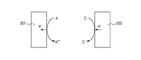
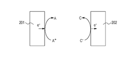
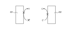
- FIGS. 2A, 2B, and 2C are conceptual diagrams for explaining charge imbalance.
- 2A, 2B, and 2C an anodic redox material and a cathodic redox material are used, and at least one of these redox materials is an EC element called a complementary type that is an EC compound.
- a complementary EC element charge imbalance may occur even with an EC element having either an anodic EC compound or a cathodic EC compound.
- 2A, 2B, and 2C have a first electrode 201 and a second electrode 202.
- An EC layer containing an anodic EC compound (A) and a cathodic EC compound (C) is disposed between the first electrode 201 and the second electrode 202.
- the anodic EC compound (A) in the decolored state is referred to as a reduced form of the anodic EC compound
- the oxidized anodic EC compound (A + ) is referred to as an oxidized form of the anodic EC compound.
- the cathodic EC compound (C) in a decolored state is referred to as an oxidized form of the cathodic EC compound, and the reduced colored state of the cathodic EC compound (C ⁇ ) is referred to as a reduced form of the cathodic EC compound.
- FIG. 2A is a diagram showing a coloring process when the EC element is in a colored state.
- a coloring voltage is applied between the first electrode 201 which is an anode electrode and the second electrode 202 which is a cathode electrode (coloring driving)
- the first electrode 201 has an anodic property represented by the formula (1).
- the oxidation reaction of the EC compound (A) proceeds.
- the reduction reaction of the cathodic EC compound (C) represented by the formula (2) proceeds.
- the reaction of the formulas (1) and (2) proceeds, the EC element is in a colored state.
- FIG. 2B is a diagram illustrating a decoloring process that is the process opposite to the coloring process.
- a decoloring voltage is applied to the first electrode 201 and the second electrode 202 (decoloring driving is performed).
- decoloring driving is performed as a decoloring driving method, for example, the first electrode 201 and the second electrode 202 are short-circuited.
- the erasing drive is performed, as shown in FIG. 2B, reverse reactions of the reactions of the equations (1) and (2) proceed.
- the reduction reaction of the oxidant (A + ) of the anodic EC compound proceeds to the reductant A at the first electrode 201, and the reductant (C ⁇ ) of the cathodic EC compound is oxidized at the second electrode 202.
- the reaction proceeds to form oxidant C.
- the colored EC compound can be returned to the decolored state.
- the cause of charge imbalance includes irreversible electron transfer reaction (electrode reaction, etc.) of the substrate involved in the redox reaction of each compound contained in the EC layer.
- electrode reaction electroreversible electron transfer reaction
- a chemical reaction with an EC compound or an environmental impurity (oxygen, water, etc.) contained in the EC layer, an impurity derived from a sealant or the like, or a chemical reaction of a radical species can be used.
- FIG. 5 is a schematic diagram illustrating the configuration of the EC device 500.
- the EC device 500 of this embodiment includes an EC element 100 and a driving unit 510.
- the configuration of the EC device is not limited to the configuration of the present embodiment, and at least the first electrode, the second electrode, and the EC layer disposed between the first electrode and the second electrode It is sufficient to have an EC element having.
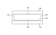
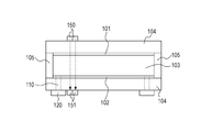
- FIGS. 1A and 1B are schematic views illustrating the configuration of the EC element 100.
- FIG. 1A and 1B are schematic views illustrating the configuration of the EC element 100.
- the EC element 100 includes a pair of substrates 104, a first electrode 101 and a second electrode 102 disposed between the pair of substrates 104, and the first electrode 101 and the second electrode 102.
- An EC layer 103 and a sealing material 105 are disposed.
- the EC layer 103 is preferably held separately from the outside by a sealing material 105.
- the EC element 100 is not limited to the configuration of this embodiment.
- the EC element 100 may not include the pair of substrates 104 and the sealing material 105, and at least the first electrode 101, the second electrode 102, the first electrode 101, and the second electrode. And the EC layer 103 disposed between them.
- the EC element 100 is a reflective EC element in which the first electrode 101 and the second electrode 102 face each other, incident light passes through the first electrode 101 or the second electrode 102 and passes through the EC element. 100 is incident.
- the EC compound contained in the EC element 100 is in a colored state, at least a part of the light is absorbed by the EC compound, is reflected by the reflector, the scatterer, etc. Emitted.
- the reflector, scatterer, and the like at this time are often arranged between the first electrode and the second electrode, but are arranged outside the electrode opposite to the electrode through which light is transmitted.
- a configuration can also be selected.
- the system through which light passes through the EC element 100 is not limited to the above-described configuration, and can be changed as appropriate according to the application.
- the pair of substrates 104 is provided with a conductive film used as the first electrode 101 or the second electrode 102.
- the pair of substrates 104 is preferably a transparent substrate.
- colorless glass, colored glass, glass such as tempered glass, a transparent polymer compound, a colorless or colored transparent resin, or the like is used.
- transparent means that the transmittance of light taken in by the EC element 100 is 50% or more and 100% or less, more preferably 70% or more and 100 or less, and further preferably 90% or more and 100% or less. Show.
- the light taken in by the EC element 100 is light in a wavelength region where the EC element 100 is to be used.
- the EC element 100 is used as an optical filter of an imaging device in the visible light region, it refers to light in the visible light region, and if used as an optical filter in an imaging device in the infrared region, the light in the infrared region is used.
- transparent resin used as the substrate 104 include polyethylene terephthalate, polyethylene naphthalate, polynorbornene, polyamide, polysulfone, polyethersulfone, polyetheretherketone, polyphenylene sulfide, polycarbonate, polyimide, and polymethyl methacrylate. Etc.
- first electrode 101 and the second electrode 102 is a transparent electrode.
- transparent indicates that the transmittance of light taken in by the EC element 100 is 50% or more and 100% or less. Since at least one of the first electrode 101 and the second electrode 102 is a transparent electrode, light is efficiently taken in from the outside of the EC element 100 and interacts with molecules of the EC compound, thereby optical characteristics of the EC compound. Can be reflected in the emitted light.
- the first electrode 101 and the second electrode 102 a layer formed by forming a transparent conductive oxide film on the substrate 104, or a conductive layer such as dispersed carbon nanotubes, a partial layer on the transparent substrate 104 is used.
- a transparent electrode or the like in which a metal wire is disposed can be used.
- transparent conductive oxides examples include tin-doped indium oxide (ITO), zinc oxide, gallium-doped zinc oxide (GZO), aluminum-doped zinc oxide (AZO), tin oxide, antimony-doped tin oxide (ATO), and fluorine-doped tin oxide.
- ITO indium oxide
- GZO gallium-doped zinc oxide
- AZO aluminum-doped zinc oxide
- tin oxide tin oxide
- antimony-doped tin oxide ATO
- fluorine-doped tin oxide FTO
- niobium-doped titanium oxide TNO
- FTO or ITO is preferable.
- each of the first electrode 101 and the second electrode 102 is preferably 10 nm or more and 10,000 nm or less.
- FTO or ITO formed in a thickness range of 10 nm to 10,000 nm is used as the first electrode 101 and the second electrode 102, both high permeability and chemical stability can be achieved.
- each electrode 101 and 102 may be an electrode layer comprised from one layer of transparent conductive oxide, or transparent It may be a laminated electrode layer in which conductive oxide sublayers are stacked.
- conductivity and transparency can be improved.
- the material of the metal wire is not particularly limited, but Ag, Au, Pt, Ti, etc. It is preferable to use an electrochemically stable metal material. Further, the arrangement pattern of the metal lines is preferably a grid.
- the transparent electrode having a metal wire may be a flat electrode, or may be curved if necessary.
- Each of the first electrode 101 and the second electrode 102 is preferably selected according to the application of the EC element 100.
- the first electrode 101 and the second electrode 102 are preferably transparent electrodes.
- the first electrode 101 and the second electrode 102 are more preferably configured using a transparent conductive oxide.
- the EC element 100 is used as a reflective EC element, one of the first electrode 101 and the second electrode 102 is a transparent electrode, and the other is a light-reflective material that reflects light taken in by the EC element 100. It is preferable to use an electrode.
- an opaque electrode or an electrode that absorbs light can be used as an electrode behind the reflective layer or the scattering layer.
- the degree of freedom of the optical characteristics of the electrode can be improved.
- each of the first electrode 101 and the second electrode 102 exists stably in the operating environment of the EC element 100, and promptly undergoes a redox reaction in response to an external voltage application. It is preferable to use a material that can advance the process.
- the distance (interelectrode distance) between the first electrode 101 and the second electrode 102 is preferably 1 ⁇ m or more and 500 ⁇ m or less. If the distance between the electrodes is large, the EC layer 103 can sufficiently contain an EC compound in an amount necessary for exerting the function required for the EC element 100. On the other hand, when the distance between the electrodes is short, the response speed can be increased.
- the EC element 100 of this embodiment may further include an electrode other than the first electrode 101 and the second electrode 102 as necessary.
- the sealing material 105 is preferably a material that is chemically stable, hardly permeates gas and liquid, and does not inhibit the redox reaction of the EC compound. Examples thereof include inorganic materials such as glass frit, organic materials such as epoxy and acrylic resins, metals, and the like. Note that the sealing material 105 may have a function as a spacer that defines and maintains the distance between the first electrode 101 and the second electrode 102.
- a spacer may be separately arranged to maintain the distance between the electrodes.
- inorganic materials such as silica beads and glass fibers, or organic materials such as polyimide, polytetrafluoroethylene, polydivinylbenzene, fluororubber, and epoxy resin can be used.
- the EC layer 103 contains an electrolyte, one or more types of EC compounds, and at least one of an oxidizable substance and a reduced substance.
- the EC layer 103 may include a layer made of an EC compound and a layer made of an electrolyte. Further, the EC layer 103 may be provided as a solution containing an EC compound and an electrolyte. In the EC element 100 according to this embodiment, the EC layer 103 may be a solution.
- the EC element 100 is a complementary EC element in which the EC layer 103 includes at least one kind of anodic redox substance and at least one kind of cathodic redox substance.
- the EC layer 103 is formed by the method described below, for example. First, the pair of substrates 104 having the first electrode 101 or the second electrode 102 and the sealing material 105 are arranged so that the first electrode 101 and the second electrode 102 face each other with a certain distance. A cell is manufactured by bonding. As shown in FIG. 1B, an opening 110 for injecting the constituent material of the EC layer 103 is formed in the cell. Next, after the constituent material of the EC layer 103 is injected from the opening 110 by a method such as a vacuum injection method, an atmospheric injection method, a meniscus method, the EC layer 103 is sealed with the sealing material 120 after the opening 110 is sealed. Can be configured.
- a method such as a vacuum injection method, an atmospheric injection method, a meniscus method
- the electrolyte contained in the EC layer 103 is the electrolyte itself or an electrolytic solution in which the electrolyte is dissolved in a solvent.
- the electrolyte for example, a solution obtained by dissolving a salt compound in a solvent, an ionic liquid, a gel electrolyte, a polymer electrolyte, or the like can be used.
- the solvent is selected according to the application in consideration of the solubility of solutes including EC compounds, oxidizable substances, and reduced substances, vapor pressure, viscosity, potential window, etc., but is a solvent having polarity. It is preferable.
- organic polar solvents such as dimethylacetamide, methylpyrrolidinone, and dioxolane.
- a polymer or a gelling agent may be contained in the above-described solvent to make the EC layer 103 a highly viscous or gelled one.
- a polymer include, but are not limited to, polyacrylonitrile, carboxymethylcellulose, polyvinyl chloride, polyethylene oxide, polypropylene oxide, polyurethane, polyacrylate, polymethacrylate, polyamide, polyacrylamide, polyester, and Nafion (registered trademark). And the like.
- the salt compound is not particularly limited as long as it is an ion dissociable salt and has a good solubility in a solvent, a high compatibility in a solid electrolyte, and a stable substance at the operating potential of an EC element. Any combination of positive ions and negative ions can be used.
- Examples of the cation include metal ions such as alkali metal ions and alkaline earth metal ions, and organic ions such as quaternary ammonium ions. Specific examples include Li, Na, K, Ca, Ba, tetramethylammonium, tetraethylammonium, and tetrabutylammonium.
- Examples of anions include anions of various fluorine compounds and halide ions. Specifically, ClO 4 ⁇ , SCN ⁇ , BF 4 ⁇ , AsF 6 ⁇ , CF 3 SO 3 ⁇ , CF 3 SO 2 NSO 2 CF 3 ⁇ , PF 6 ⁇ , I ⁇ , Br ⁇ , Cl ⁇ and the like. Is mentioned.
- an EC compound which is also a salt compound it is possible to serve as both an EC compound solution and an electrolyte solution.
- Examples of EC compounds that are also salt compounds include viologen derivatives.
- the EC compound used in the present embodiment is an organic compound including a low molecular organic compound and a high molecular organic compound.
- Examples of the polymer organic compound that can be used as the EC material include a polymer compound containing a pyridinium salt, and specific examples thereof include a viologen-based polymer compound.
- the EC compound of the present embodiment it is preferable to use a low molecular organic compound having a molecular weight of 2000 or less and a compound that changes from a decolored body to a colored body by an oxidation reaction or a reduction reaction at an electrode.
- the anodic EC compound and the cathodic EC compound are included as the EC compound, but the present invention is not limited thereto, and it is sufficient that at least one of them is included.
- the anodic EC compound or cathodic EC compound contained in the EC layer 103 may be one kind or plural kinds.
- anodic EC compound for example, amines having an aromatic ring (for example, phenazine derivatives, triallylamine derivatives), thiophene derivatives, pyrrole derivatives, thiazine derivatives, triallylmethane derivatives, bisphenylmethane derivatives, xanthene derivatives, fluorane derivatives And spiropyran derivatives and the like.
- amines having an aromatic ring for example, phenazine derivatives, triallylamine derivatives
- thiophene derivatives for example, phenazine derivatives, triallylamine derivatives
- pyrrole derivatives for example, phenazine derivatives, thiophene derivatives, pyrrole derivatives, thiazine derivatives, triallylmethane derivatives, bisphenylmethane derivatives, xanthene derivatives, fluorane derivatives And spiropyran derivatives and the like.
- a low molecular thiophene derivative for example, a monothiophene derivative, an oligothiophene derivative, a thienoacene derivative
- an amine having a low molecular aromatic ring for example, a phenazine derivative or a triallylamine derivative
- the above-mentioned anodic EC compound has an absorption peak in the ultraviolet region in the neutral state, does not absorb in the visible light region, and takes a decolored state with high transmittance in the visible light region. Moreover, the above-mentioned anodic EC compound becomes a radical cation by an oxidation reaction, and becomes a colored body by shifting absorption to the visible light region.
- the absorption wavelength of these molecules can be designed by enlarging or reducing the ⁇ -conjugate length and changing the substituent to change the ⁇ -conjugated system.
- cathodic EC compounds examples include pyridine compounds such as viologen and quinone compounds.
- the EC compound of this embodiment is dissolved in the electrolyte.
- the EC element 100 only needs to be able to transfer charges between electrodes when performing charge rebalancing. For this reason, the EC compound may not be configured to diffuse through the electrolyte.
- the EC compound may be fixed to each of the first electrode 101 and the second electrode 102.
- a method of immobilizing the EC compound As a specific method of immobilizing the EC compound, a method of bonding to the electrode material via a functional group contained in the EC compound, or a film state using the force such as electrostatic interaction, etc. And a method of physically adsorbing an EC compound on an electrode.
- a method of chemically bonding an EC compound to a porous electrode through a functional group of the molecule or a method of forming an EC compound on the electrode is preferable.
- the EC compound As a method of chemically bonding the EC compound to the porous electrode through the functional group of the molecule, through the functional group such as phosphate group and carboxylic acid group, on the oxide fine particle electrode such as titanium oxide, zinc oxide, tin oxide, There is a method of immobilizing a low molecular weight organic compound which is an EC compound.
- the method for forming the EC compound on the electrode include a method for polymerizing and forming a viologen polymer on the transparent electrode.
- the anodic EC compound becomes a colored body by a reversible first oxidation reaction, and becomes a decolored body by a reduction reaction that is the reverse reaction of the first oxidation reaction.
- the EC compound that has become a colored product by the first oxidation reaction may further deteriorate due to the occurrence of a second irreversible oxidation reaction.
- the cathodic EC compound becomes a colored body by a reversible first reduction reaction, and becomes a decolored body by an oxidation reaction which is the reverse reaction of the first reduction reaction.
- the anodic EC compound that has become a colored product by the first reduction reaction may further deteriorate due to the occurrence of a second irreversible reduction reaction.
- An oxidizable substance is a substance that undergoes an irreversible oxidation reaction electrochemically.
- the substance to be reduced is a substance in which an irreversible reduction reaction proceeds electrochemically.
- the EC element 100 performs charge rebalancing using an irreversible oxidation reaction of an oxidizable substance or an irreversible reduction reaction of a oxidizable substance, thereby reducing the color residue in the decolored state and the absorption spectrum in the colored state. Reduce change.
- the EC layer 103 includes at least one of an oxidizable substance in which an electrochemical oxidation reaction proceeds irreversibly and a reduced substance in which an electrochemical reduction reaction proceeds irreversibly.
- the substance to be oxidized is a substance that is irreversibly oxidized when a predetermined voltage is applied to the EC layer 103 from a state where the EC layer 103 is transparent (initial state).
- An irreversibly oxidized substance, that is, an oxidant of an oxidizable substance is not easily reduced.
- the substance to be reduced is a substance that is irreversibly reduced when a predetermined voltage is applied to the EC layer 103 from the initial state. Similar to the substance to be oxidized, the reduced form of the substance to be reduced is not easily oxidized.
- the irreversible oxidation reaction of the oxidizable substance is less likely to occur in potential than the reversible first oxidation reaction in which the EC compound becomes colored.
- the irreversible oxidation reaction of the oxidizable substance of the present embodiment is more likely to occur in potential than the irreversible second oxidation reaction that leads to deterioration of the EC compound.
- the oxidizable substance of this embodiment is not colored when irreversibly oxidized.
- the substance to be reduced according to the present embodiment is less likely to cause an irreversible reduction reaction than a reversible first reduction reaction in which the EC compound is colored.
- the irreversible reduction reaction of the substance to be reduced according to the present embodiment is more likely to occur in potential than the irreversible second reduction reaction that leads to deterioration of the EC compound.
- it is preferable that the to-be-reduced substance of this embodiment is not colored when it is irreversibly reduced.
- the EC layer 103 of the present embodiment includes at least one of an oxidizable substance that satisfies the following conditions (A) to (D) and a reduced substance that satisfies the conditions (E) to (H). .
- the substance to be oxidized is “not colored” means that the maximum absorbance when irreversibly oxidized is not more than 1/10 of the maximum absorbance in the maximum coloring state of the EC element 100, more preferably not more than 1/100, More preferably, it is defined as 1/1000 or less.
- the substance to be reduced is “not colored” means that the maximum absorbance when irreversibly reduced is 1/10 or less, more preferably 1/100 or less of the maximum absorbance in the maximum coloring state of the EC element 100. More preferably, it is defined as 1/1000 or less.
- the “maximum absorbance” is the greatest absorbance in the wavelength region targeted by the EC element 100.
- the substance to be oxidized satisfies the following condition (i).
- the conditions (F) and (G) are replaced with the oxidation-reduction potential, the substance to be reduced satisfies the following condition (ii).
- the potential VO1 irreversibly oxidized includes a potential VA1 at which the anodic EC compound contained in the EC layer 103 is reversibly oxidized, and a potential VA2 at which the anodic EC compound is irreversibly oxidized. Between.
- a potential VR1 irreversibly reduced is a potential VC1 at which the cathodic EC compound contained in the EC layer 103 is reversibly reduced; a potential VC2 at which the cathodic EC compound is irreversibly reduced; Between.
- Examples of oxidizable substances that satisfy the conditions (A) to (D) or reduced substances that satisfy the conditions (E) to (H) include primary amine compounds, secondary amine compounds, tertiary amine compounds, aromatic amine compounds, Examples thereof include nitrogen-containing compounds such as heterocyclic compounds containing a nitrogen atom. Examples of the heterocyclic compound containing a nitrogen atom include pyridine salt derivatives.
- a reversible oxidation reaction (hereinafter referred to as a reversible oxidation reaction different from the first oxidation reaction) at a potential between a potential at which a reversible first oxidation reaction occurs and a potential at which an irreversible second oxidation reaction occurs. , Referred to as “third oxidation reaction”). Since the third oxidation reaction is a reversible reaction, even if the potential VO1 is a potential at which the first oxidation reaction of the EC compound proceeds and the third oxidation reaction of the EC compound does not proceed, The potential may be such that the third oxidation reaction proceeds and the irreversible second oxidation reaction does not proceed.
- the cathodic EC compound has a reversible potential different from that of the first reduction reaction at a potential between the potential at which the reversible first reduction reaction occurs and the potential at which the irreversible second reduction reaction occurs.
- a reduction reaction (third reversible reaction) may occur. Since the third reduction reaction is a reversible reaction, even if the potential VR1 is a potential at which the first reduction reaction of the EC compound proceeds and the third reduction reaction of the EC compound does not proceed, The potential may be such that the third reduction reaction proceeds and the irreversible second reduction reaction does not proceed.
- the EC layer 103 contains an oxidizable material if the EC compound that becomes a colored residue due to charge imbalance is an anodic EC compound, and the EC layer 103 if the EC compound that becomes a colored residue due to charge imbalance is a cathodic EC compound. Preferably it contains a reducing substance. When both the anodic EC compound and the cathodic EC compound can be colored remnants, the EC layer 103 preferably contains an oxidizable substance and a reduced substance.
- the oxidizable substance and the reducible substance are contained in the EC layer 103 in a state where they are dissolved or dispersed in the electrolyte, or fixed on an immobilization carrier.
- the quantitative range in which charge rebalancing can be performed using an oxidizable substance or a reducible substance is proportional to the amount of the oxidizable substance or reducible substance present in the system. Therefore, it is preferable that the oxidizable substance and the reduced substance are contained in the EC layer 103 by dissolution or dispersion.
- the substance to be oxidized and the substance to be reduced be dissolved in the electrolyte, move freely in the electrolyte in the EC layer 103, and reach the first electrode 101 or the second electrode 102.
- the substance to be oxidized and the substance to be reduced are allowed to move freely in the electrolyte, there is no need for an immobilization carrier for immobilizing the substance to be oxidized and the substance to be reduced. Can contribute. Further, when the oxidizable substance and the reducible substance are immobilized, the amount of the oxidizable substance and the reducible substance that can be immobilized may be limited depending on the surface area of the immobilization support. In the case of dissolving an oxidizable substance and a reduced substance in the electrolyte, there is a limit on the solubility and the like, but the limit of the amount of the oxidized substance and the reduced substance contained in the EC layer 103 is smaller than the case of fixing. . Therefore, more oxidizable substances and reducible substances can be present in the system by the method of dissolving the oxidizable substances and reducible substances in the electrolyte.
- FIG. 5 is a schematic diagram illustrating an example of the configuration of the driving unit 510.
- the driving unit 510 is a unit that controls the transmittance of the EC element 100 by pulse width modulation, and includes a driving power source 501, a resistance switching unit 502, a control unit 503, and an acquisition unit 504.
- the driving unit 510 maintains the transmittance of the EC element 100 without changing the peak value of the pulse voltage waveform, and changes the EC voltage application period ratio (Duty ratio) in one cycle of the pulse voltage waveform.
- the transmittance of the element 100 is controlled.
- the potential changes. Thereby, the state of the oxidation-reduction reaction of each compound in the EC layer 103 can be changed.
- the drive power supply 501 applies a voltage necessary for causing an electrochemical reaction in the EC layer 103 to the EC element 100.
- the absorption spectrum may change due to a difference in redox potential or molar extinction coefficient of the EC compound.
- the voltage application start of the drive power source 501 or the application state is maintained by a signal from the control unit 503. In the present embodiment, the application state of a constant voltage is maintained during the period in which the light transmittance of the EC element 100 is controlled.
- the resistance switching unit 502 switches the resistor R1 and the resistor R2 larger than the resistor R1 in a closed circuit including the driving power source 501 and the EC element 100 and connects them in series.
- the resistance value of the resistor R1 is preferably at least smaller than the largest impedance of the element closed circuit, and is preferably 10 ⁇ or less.
- the resistance value of the resistor R2 is preferably larger than the largest impedance of the element closed circuit, and is preferably 1 M ⁇ or more.
- the resistor R2 may be air. In this case, strictly speaking, the closed circuit is an open circuit, but it can be considered as a closed circuit by regarding air as the resistance R2.
- Control Unit 503 sends a switching signal to the resistance switching unit 502 and controls switching of the resistors R1 and R2.
- a coloring reaction occurs in the EC element when the resistance is R1, and a coloring reaction does not occur in the EC element when the resistance is R2.
- the EC material undergoes self-decoloration. This self-decoloration phenomenon is caused by instability of radical species of EC material caused by coloring reaction, diffusion to a counter electrode having different potentials, collision of radical species of anode material and radical species of cathode material in a solution, etc. to cause.
- the absorbance is maintained where the coloring amount and the self-decoloring amount are balanced.
- the organic EC element is driven with the duty ratio fixed under a constant voltage of the drive power source 501, the change in absorbance is saturated through a transient state, and the saturated absorbance is maintained.
- the duty ratio may be fixed to a smaller duty ratio than the immediately preceding duty ratio.
- the duty ratio may be fixed to be larger than the immediately preceding duty ratio.
- one cycle is preferably 100 milliseconds or less, and more preferably 10 milliseconds or less.
- the means for driving the EC element 100 is not limited to the method of adjusting the transmittance according to the duty ratio, but the method of changing the peak value of the voltage, the method of applying the erase voltage during the period of the resistor R2, or the short circuit during the period of the resistor R1. It is possible to appropriately use the method of
- the acquisition unit 504 acquires charge balance information in the EC element 100. Based on the information acquired by the acquisition unit 504, the control unit 503 controls the voltage applied to the EC element 100 by the drive power source 501. As a method for acquiring the information on the charge balance in the acquisition unit 504, there are a detection unit for detecting the charge balance of the EC layer 103, an input unit for the user to input information, and the like. Details of the charge balance detection method in the acquisition unit 504 will be described later.
- each component of the drive unit 510 is arranged is not particularly limited.
- a part or all of the configuration of the driving unit 510 may be arranged on a window frame or the like.
- a constituent member of an apparatus using an EC element may be used in common.
- the control unit of the imaging apparatus may have the function of the control unit 503. With such a configuration, it is possible to contribute to downsizing of the apparatus. If the respective components of the EC device 500 are configured integrally, even when the EC elements are exchanged, an operation reflecting characteristics specific to each EC element can be realized.
- the oxidation (or reduction) reaction of the oxidized (or reduced) substance is It is preferably less likely to occur than one oxidation (or reduction) reaction.
- the anodic (or cathodic) EC compound is reduced (or oxidized) and decolored.
- the voltage applied to the first electrode 101 and the second electrode 102 is changed to irreversibly oxidize (or reduce) the substance to be oxidized (or to be reduced).
- a second oxidation (or reduction) reaction occurs in which a normal anodic (or cathodic) EC compound is irreversibly oxidized (or reduced).
- EC compounds that can be used for coloring the EC element 100 are reduced, and there is a possibility that poor coloration and decoloration failure due to the irreversibly oxidized (or reduced) EC compound becoming a colored body may occur. Therefore, in order to prevent the irreversible oxidation (or reduction) of the EC compound, the oxidation (or reduction) reaction of the oxidized (or reduced) substance is more likely to occur than the second oxidation (or reduced) reaction. Is preferred.
- the reaction includes a reaction in which an anodic (or cathodic) EC compound remaining in a colored state in the other electrode is reduced (or oxidized), and a cathodic property that is reduced (or oxidized) in the EC layer 103. Examples thereof include a reaction in which (or anodic) EC compound reacts with the remaining colored body to reduce (or oxidize) the remaining colored body.
- the substance to be oxidized (or reduced) When the substance to be oxidized (or reduced) is oxidized (or reduced) to become a colored body, the shape of the absorption spectrum of the EC element 100 in the colored state and the transparency in the decolored state are affected. Therefore, it is preferable to select a substance to be oxidized (or reduced) that does not color the oxidized form (or reduced form). That is, the substance to be oxidized (or reduced) satisfies the above condition (D) (or condition (H)).
- the EC element 100 irreversibly oxidizes a substance to be oxidized that satisfies the conditions (A) to (D) when an “anodic charge imbalance” occurs in which the anodic EC compound becomes a remaining colored body.
- an “anodic charge imbalance” occurs in which the anodic EC compound becomes a remaining colored body.
- electrons are supplied to perform charge rebalancing.
- a reducible substance that satisfies the conditions (E) to (H) receives electrons and is irreversible. The charge is rebalanced by reducing to.
- the potential at which each of the redox substance such as an EC compound, the oxidized substance, and the reduced substance is oxidized and reduced is not limited to a point and may vary. Therefore, even when an oxidizable (reduced) substance that satisfies the condition (i) (or (ii)) is used, the oxidizable (or reduced) substance is also reversible when the EC compound is reversibly oxidized (or reduced). It may be oxidized (or reduced). In addition, the EC compound may be irreversibly oxidized (or reduced) when the oxidized (or reduced) substance is oxidized (or reduced).
- the potential difference with VC1) is 100 mV or more.
- the potential difference between the potential VO1 (or VR1) and the potential VA1 (or VC1) is more preferably 200 mV or more.
- the potential difference between the potential VO1 (or VR1) and the potential VA2 (or VC2) at which the second oxidation (or reduction) reaction of the anodic (or cathodic) EC compound occurs is preferably 100 mV or more, more preferably Is 200 mV or more.
- a driving method of the EC device 500 will be described.
- the first voltage V ⁇ b> 11 is applied between the first electrode 101 and the second electrode 102.
- the first potential V21 when the first voltage V11 is applied is such that the first oxidation-reduction reaction in which the EC compound becomes a colored body proceeds, and the irreversible oxidation reaction of the oxidant or the reductant The potential at which the irreversible reduction reaction does not proceed.
- the acquisition unit 504 appropriately acquires charge balance information in the EC element 100.
- the control unit 503 changes the drive voltage from the drive power source 501 from the first voltage V11 that is the first potential V21 to the second voltage V12 that is the second potential V22 based on the information of the acquisition unit 504. .
- the control unit 503 controls the drive power source 501 to change the potential when it is determined from the detection result of the detection unit as the acquisition unit 504 that charge imbalance has occurred.
- the occurrence of charge imbalance may refer to the transmittance during decoloring or the transmittance during coloring.
- the transmittance at the time of decoloring preferably refers to the transmittance in a state where the element is driven at the maximum transmittance.
- the transmittance at the time of coloring it is preferable to refer to the transmittance in a state where the element is driven with the minimum transmittance.
- the driving power source 501 applies the second voltage V12 to the EC element 100 so that the irreversible oxidation or reduction reaction of the oxidizable substance and the reduced substance proceeds. Thereby, the oxidation-reduction reaction for the above-mentioned charge rebalance proceeds.
- the second potential V22 is a potential at which an irreversible oxidation or reduction reaction of the substance to be oxidized and the substance to be reduced occurs and an irreversible second oxidation-reduction reaction of the EC compound does not occur.
- the control unit 503 changes the voltage to the first voltage V11.
- the timing for performing charge rebalancing is not particularly limited, but it is preferable to acquire charge balance information from the EC element 100 in a decolored state and appropriately perform charge rebalance based on the information. This is because the colored EC compound that remains even after a sufficient time has elapsed after the EC element 100 is driven to be decolored is considered to be basically caused by charge imbalance.
- the potential difference between the potential applied at this time and the potential at the time of decoloring driving is within a range that does not adversely affect the components of the EC element 100 such as a deterioration reaction of the EC compound and the electrolyte contained in the EC layer 103. Will be set. Specifically, the potential difference is such that an irreversible reaction of the EC compound contained in the EC element 100 does not proceed while an oxidation reaction of the oxidizable substance or a reduction reaction of the reduced substance proceeds. It should be noted that increasing the absolute value of the applied voltage when performing charge rebalancing is advantageous in that the electrode reaction necessary for charge rebalancing is promoted.
- reducing the absolute value of the applied voltage when performing charge rebalancing is advantageous in that it can suppress adverse effects on the EC compound and increase in power consumption. It is preferable that the range of the voltage applied when performing charge rebalancing is appropriately set according to the characteristics of the device, the usage environment, and the like.
- the driving method for performing charge rebalancing is described in terms of voltage control for controlling the applied voltage.
- the driving method of the present invention is not limited to voltage control, and is a current control (charge amount control) control method as long as the first potential V21 and the second potential V22 of the EC element 100 are in a predetermined potential range. Can also be used.
- charge rebalancing can be performed by the following method.
- the EC element 100 is brought into a normal full coloring state, and a current value flowing between the first electrode 101 and the second electrode 102 at that time is measured. Thereafter, the current value between the first electrode 101 and the second electrode 102 is controlled so that a current exceeding the current value flows.
- the potential difference applied between the first electrode 101 and the second electrode 102 causes the first oxidation (or reduction) in which the anodic (or cathodic) EC compound is reversibly oxidized (or reduced).
- a potential difference is generated where the substance to be oxidized (or reduced) is oxidized (or reduced), and charge rebalancing proceeds.
- the degree of the current value exceeding the fully colored state at this time varies depending on the concentration ratio of the EC compound added to the EC element and the substance to be oxidized (or reduced). As an example, a range of 101% to 200% of the current value in the fully colored state can be given.
- the voltage or current applied in the voltage or current application step for charge rebalancing is larger than the voltage or current applied when coloring the electrochromic device. It can be said that the electrochromic device is given more energy than the normal driving in charge rebalance.
- the voltage application time for charge rebalancing depends on the value of the applied voltage. Basically, the voltage application time for charge rebalancing is longer than the time when the electric double layer is formed on the electrode surface and the Faraday current begins to flow, and the charge balance exceeds the normal point and has the opposite polarity. It is preferably shorter than the period until imbalance occurs. Note that the voltage application time varies depending on the value of the applied voltage. The voltage application time depends on the response speed of the EC element 100 and the like, but can be set to 1 ms or more and 10 seconds or less as an example. It is also preferable to select the next application time and the applied voltage based on the charge balance of the EC element 100 after the voltage is applied for a short time.
- the voltage application pattern to be applied for charge rebalancing is preferably applied continuously or with a pattern such as a pulse shape, and it is preferable to apply the voltage in a pulse shape.
- the information on the charge balance of the EC element 100 may be acquired, and the polarity and magnitude of the voltage to be applied may be determined based on the information.
- the means for acquiring the information on the charge balance will be described below.
- the acquisition unit 504 acquires charge balance information by, for example, means for detecting the charge balance of the EC layer 103 using light absorption of an EC compound, or using electrode potential measurement. There are means for detecting the charge balance of the layer 103.
- Detection means using light absorption As means for detecting charge balance using light absorption of an EC compound, each characteristic of an anodic EC compound and a cathodic EC compound contained in the EC layer 103 is used. There are measuring means for measuring the amount of light absorption at various absorption wavelengths.
- FIG. 1B shows an example of the configuration of the EC element 100 having a measuring means for measuring the amount of light absorption.
- the EC element 100 includes two light sources 150 and two detectors 151 that detect light emitted from each of the two light sources 150 and passing through the EC element 100.
- the amount of light absorption in the decolored state increases or the ratio of the amount of light absorption in the colored state changes, so that the charge balance can be detected from the amount of light absorption. .
- the amount of change in light absorption from the amount of light absorption in the decolored state in the initial state is obtained, and if the amount of change in light absorption exceeds a threshold value, it is determined that charge imbalance has occurred. .
- the amount of change in the light absorption amount the difference or ratio between the light absorption amount in the decolored state in the initial state and the light absorption amount appropriately measured can be used.
- the light source 150 to be used is preferably a light source that can emit light having an intensity necessary for detecting the balance of charges and does not affect the characteristics of the EC element 100 as an application.
- the plateau 150 emits light having characteristic absorption wavelengths of the anodic EC compound and the cathodic EC compound.
- an LED or the like can be used as the light source 150.
- the detection unit 151 may have any sensitivity necessary for detecting the balance of electric charges and does not adversely affect the characteristics of the EC element 100 as an application.
- a light receiving element such as a photodiode is used. Can be mentioned.
- the electrode potential of the first electrode 101 and / or the second electrode 102 is determined using a reference electrode or the like.
- An example is a measuring method.
- the case where the anodic EC compound is a residual color body will be described in detail. The following explanation also applies to the case where the color of the cathodic EC compound remains if the polarity is reversed. Therefore, the case where the cathodic EC compound becomes the remaining colored body is indicated by “or” in parentheses. There are things to do.
- the cathodic (or anodic) EC compound in the EC layer 103 is almost reduced (or oxidized) and becomes decolored. Therefore, it is considered that the potential of the first electrode 101 and / or the second electrode 102 in the decolored state is defined by the ratio of the oxidant and the reductant of the anodic (or cathodic) EC compound.
- the material used as the EC compound preferably exhibits redox characteristics with high reversibility. This is because using a material that does not exhibit high reversibility reduces the responsiveness and durability of the EC element and increases power consumption. Therefore, when there is a residual colored body, the potential of the first electrode 101 or / and the second electrode 102 is proportional to the natural logarithm of the activity ratio of the oxidant and the reductant according to the Nernst equation, The value deviated from the standard electrode potential of the anodic (or cathodic) EC compound is shown. The activity ratio between the oxidant and the reductant can be approximately replaced with the concentration ratio between the oxidant and the reductant. By utilizing this, the charge balance can be detected.
- the potential of the first electrode 101 and / or the second electrode 102 can be determined based on which of the redox potential of the anodic EC compound or the cathodic EC compound is close. For example, if the electrode potential is close to the redox potential of the cathodic EC compound, it can be determined that the charge balance is inclined in the direction in which the cathodic EC compound remains in color. That is, it can be determined that an anodic (or cathodic) charge imbalance has occurred.
- the charge balance is determined by measuring how much the potential of the first electrode 101 or the second electrode 102 is shifted in which direction from the oxidation-reduction potential of the EC compound immobilized on the electrode. be able to.
- the potential of the electrode on which the cathodic EC compound is immobilized is sufficiently positive compared to the oxidation-reduction potential, and most of the cathodic EC compound is present. Is considered to be an oxidant (decolorant).
- the potential of the electrode on which the anodic EC compound is immobilized is close to the redox potential of the anodic EC compound, and it is considered that the oxidant and the reductant of the anodic EC compound coexist.
- an input unit that inputs information that the user visually determines the presence or absence of charge imbalance from the coloring state of the EC element 100 may be used. For example, when the user determines that charge imbalance has occurred, if information indicating that charge imbalance has occurred is input to the input means, the control unit 503 changes the voltage of the drive power source 501 based on the information. To do. In that case, a dedicated button or the like disposed at a position where the user can operate may be used as the input means.
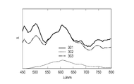
- FIG. 3B shows an absorption spectrum of the EC element 100 in a colored state or a decolored state.
- FIG. 3B is a diagram illustrating an absorption spectrum of the EC element 100 in a colored state or a decolored state.
- FIG. 3A shows an absorption spectrum of an EC element in which the EC layer does not contain an oxidizable substance and a reduced substance.
- FIGS. 3A and 3B is a result of calculating an absorption spectrum of a complementary EC element by calculation.
- the anodic EC compound was a compound having absorption peaks at 455 nm and 500 nm
- the cathodic EC compound was a compound having an absorption peak at 605 nm.
- the absorption spectrum of the EC element 100 in the colored state is the same as the absorption spectrum (the spectrum 301 in FIG. 3A) of the EC element in which the EC layer in the colored state does not include an oxidizable substance and a reduced substance. .
- the absorption spectrum in the colored state of each EC element is as shown by a spectrum 303 in FIG. 3A and a spectrum 312 in FIG. 3B.
- the cathodic charge imbalance occurs as in the spectra 303 and 312
- the absorption at 455 nm and 500 nm derived from the anodic EC compound is relatively lowered as compared with the spectrum 301 in the normal state.
- an absorption spectrum in a colored state of the EC element 100 is a spectrum. It becomes like 313.
- the spectrum 313 substantially coincides with the absorption spectrum 301 when the charge balance is normal, and the change in the shape of the absorption spectrum in the colored state is reduced by performing charge rebalancing using an oxidizable substance or a reduced substance. You can see that.
- a first oxidant (or oxidant) obtained by subjecting an anodic (or cathodic) EC compound to a first oxidation (or reduction) reaction ( Or the first reductant) is brought into direct contact with the corresponding oxidized (or reduced) substance.
- the first oxidant (or first reductant) is a colored body.
- a corresponding oxidizable (or reducible) substance is put into a solution containing an electrolyte in which a first oxidant (or reductant) of an anodic (or cathodic) EC compound is dissolved.
- a first oxidant (or reductant) of an anodic (or cathodic) EC compound is dissolved.
- the oxidation (or reduction) reaction of the oxidizable (or reducible) substance is performed on the anodic (or cathodic) EC compound. It can be confirmed that it is less likely to occur than the first oxidation (or reduction) reaction. That is, it can be confirmed that the substance to be oxidized (or reduced) satisfies the above-mentioned condition (B) (or (F)).
- the method described below is a method of measuring the electrode reaction potential of the EC compound, the oxidizable substance, and the reduced substance, and comparing the electrode reaction potential.
- the oxidation-reduction potential can be determined by electrochemical measurement. For example, it can be measured by performing cyclic voltammogram measurement (hereinafter referred to as “CV measurement”) of the EC compound, the oxidizable substance, and the reduced substance.
- CV measurement cyclic voltammogram measurement
- the potential at which the oxidation (or reduction) reaction of the oxidized (or reduced) substance occurs from the potential at which the current due to the second oxidation (or reduction) reaction of the anodic (or cathodic) EC compound occurs. If it is on the negative (or positive) side, the condition (C) (or (G)) is satisfied.
- a working electrode and a counter electrode are prepared.
- the working electrode an electrode made of the same material as the electrode of the EC element 100 is preferably used.
- the working electrode is an electrode having ITO.
- the counter electrode for example, a platinum electrode having a sufficient area is preferably used.
- a solvent or supporting electrolyte used when performing CV measurement it is preferable to use the solvent or supporting electrolyte contained in the EC layer 103. Further, it is preferable that the running speed of the voltammogram is appropriately set, for example, in the range of 20 mVs ⁇ 1 to 200 mVs ⁇ 1 .
- the EC element 100 of the present embodiment at least one of the oxidizable material satisfying the conditions (A) to (D) and the reducible material satisfying the conditions (E) to (H) is used as the EC layer.
- charge rebalancing can be performed. As a result, it is possible to reduce the remaining colored body and to reduce the color residue in the decolored state of the EC element and the change in the absorption spectrum in the colored state.
- the EC element 100 of the present embodiment when no color residue is generated in the decolored state, a voltage is applied so that the first redox reaction of the EC compound proceeds to correct the charge imbalance. At this time, the potential may be increased. Therefore, an increase in power consumption can be suppressed.
- the EC element including the redox buffer of Patent Document 1 can reduce the color residue in the decolored state.
- the method of Patent Document 1 cannot perform charge rebalance. Therefore, in the colored state, the ratio of the colored body of the anodic EC compound and the colored body of the cathodic EC compound may change, and the absorption spectrum may change.
- charge rebalancing can be performed, so that changes in the shape of the absorption spectrum during coloring can be reduced.
- the redox buffer is more easily oxidized and reduced than the EC compound contained in the EC element, power consumption for driving the EC element to be colored is increased, and the response speed may be lowered.
- the EC device 500 of the present embodiment it is only necessary to oxidize a substance to be oxidized or to reduce a substance to be reduced only when charge rebalancing is performed. Can be reduced.
- an excessive voltage is applied to the EC layer in addition to the method using an irreversible reaction of an oxidizable substance or a reduced substance as in this embodiment, and the EC layer It is also conceivable to irreversibly decompose the EC compound contained in.
- FIG. 4 shows the relationship between the coloring density of the EC layer in the colored state and the number of times of EC compound charge rebalancing.
- the color density (R) of the EC layer is the vertical axis
- the number of charge rebalances (N) is the horizontal axis
- the charge rebalance is performed by the method of this embodiment.
- the case where the charge rebalance is performed by irreversible decomposition of the EC compound is indicated by a triangle. Note that the amount of charge rebalance once is 0.1% of the entire EC compound.
- the irreversible decomposition of the EC compound when the irreversible decomposition of the EC compound is performed, the color density of the EC layer decreases as the number of implementations increases, whereas in the method of this embodiment, the color density is almost reduced. do not do.
- the EC element 700 of this embodiment will be described with reference to FIG.
- the EC element 700 is an EC element having a third electrode 730.
- 7A is a top view illustrating the configuration of the EC element 700
- FIG. 7B is a cross-sectional view illustrating the configuration of the EC element 700.
- the EC element 700 includes a first electrode 701, a second electrode 702, an EC layer 703, a substrate 704, a sealing material 705, and a third electrode 730.
- a first electrode 701 and a second electrode 702 are arranged to face each other between a pair of substrates 704, and an EC layer 703 is arranged between the first electrode 701 and the second electrode 702. ing.
- the sealant 705 is disposed between the pair of substrates 704, and a cell is formed by the pair of substrates 704 and the sealant 705.
- An opening 710 is provided in the cell, and the opening 710 is sealed with a sealing material 720. Since the first electrode 701, the second electrode 702, the EC layer 703, the substrate 704, and the sealant 705 are the same as the corresponding constituent members in the first embodiment, detailed description thereof is omitted.
- the third electrode 730 is an electrode that performs an irreversible oxidation reaction of the substance to be oxidized or an irreversible reduction reaction of the substance to be reduced for charge rebalancing.
- a configuration may be adopted in which a third electrode 730 is provided as necessary, and a reaction for charge rebalancing is performed by the third electrode 730.
- the oxidizable substance is irreversibly oxidized, or the reduced substance is irreversibly reduced. Therefore, the oxidized or reduced substance is adsorbed on the first electrode and the second electrode, and the oxidation-reduction reaction of the EC compound is inhibited, or the transparency of the EC layer is lowered. Can be reduced.
- the material used as the third electrode 730 is not particularly limited, and the same material as the first electrode 101 or the second electrode 102 of the first embodiment can be used.
- a material having a porous structure with a large effective area can be used as necessary. By increasing the effective area, it is possible to reduce the projected area of the third electrode 730, which can contribute to downsizing of the EC element 700.
- Materials having a porous structure that can be used as the third electrode 730 include conductive oxides such as tin-doped indium oxide (ITO), zinc oxide, gallium-doped zinc oxide (GZO), aluminum-doped zinc oxide (AZO), and oxidation.
- conductive oxides such as tin-doped indium oxide (ITO), zinc oxide, gallium-doped zinc oxide (GZO), aluminum-doped zinc oxide (AZO), and oxidation.
- Tin antimony-doped tin oxide (ATO), fluorine-doped tin oxide (FTO), niobium-doped titanium oxide (TNO), titanium oxide, a porous carbon material, a porous metal film, or a combination of these, etc.
- ATO antimony-doped tin oxide
- FTO fluorine-doped tin oxide
- TNO niobium-doped titanium oxide
- titanium oxide a porous carbon material, a
- the porous structure preferably has a nanometer-scale microstructure from the viewpoint of production.
- Nano structure bodies such as a nanoparticle film
- a particle film having a large specific surface area per volume and easy to produce is preferably used.
- the size of the particles used for forming this particle film the average particle diameter is preferably 300 nm or less, more preferably 50 nm or less.
- the conductive electrode that scatters light not only the above-described transparent conductive oxide, A porous conductor, a carbon material, or a metal such as platinum or titanium can be used.
- first electrode 701, the second electrode 702, and the third electrode 730 will be described.
- an arrangement method generally known as an electrode arrangement of the EC element 700 can be used.
- the first electrode 701 and the second electrode 702 formed on the substrate 704 are opposed to each other, and an interelectrode distance of about 1 ⁇ m to 500 ⁇ m is provided. There is a method.
- the material of the third electrode 730 is a material having a low visible light transmittance such as a metal or carbon having a porous structure, the light transmittance of the EC layer 703 is significantly reduced by the third electrode 730. There is a risk. Even when a material having high transmittance is used as the material of the third electrode 730, if there is a difference in refractive index between the third electrode 730 and the electrolyte, light transmittance in the EC layer 703 is caused by scattering or the like. May be reduced. Therefore, it is preferable that the third electrode 730 be disposed outside the optical path of light that passes through at least one of the first electrode 701 and the second electrode 702.
- out of the optical path means that when the EC element is used as a light absorbing element, it is out of the optical path of the target light.
- a case where an EC element is used as a transmission filter of an imaging apparatus will be described as an example. In that case, out of all the light transmitted through the EC element, out of the optical path for the light reaching the area used for imaging in the entire area of the light receiving element (for example, CCD sensor, CMOS sensor) of the imaging device It is preferable to arrange the third electrode 730 at the position. By disposing the third electrode 730 outside the optical path, the degree of freedom in selecting the constituent material of the third electrode 730 can be improved. Further, by performing the reaction for charge rebalancing at the third electrode 730, the influence of the irreversibly oxidized irreversible substance or the irreversibly reduced reducible substance on the permeability of the EC element 700. Can be reduced.
- the EC element of this embodiment is the same as that of the first embodiment except that the EC layer 103 of the first embodiment further includes a redox substance that satisfies the following conditions (a) to (c) or (d) to (f). This is the same as the embodiment.
- the EC layer 103 includes a plurality of redox substances that undergo a reversible redox reaction electrochemically.
- the plurality of redox substances include at least one EC compound and a redox substance that satisfies the following conditions (a) to (c) or (d) to (f).
- the EC layer 103 may further contain one or more types of other EC compounds.
- the EC layer 103 may contain a plurality of redox substances that satisfy the conditions (a) to (c) or (d) to (f).
- (B) The reversible oxidation reaction is less likely to occur than the reversible oxidation reaction in which the anodic EC compound contained in the EC layer is colored.
- (C) A reversible oxidation reaction is more likely to occur than an irreversible oxidation reaction of the anodic EC compound contained in the EC layer.
- (E) A reversible reduction reaction is less likely to occur than a reversible reduction reaction in which the cathodic EC compound contained in the EC layer is in a colored state.
- (F) A reversible reduction reaction is more likely to occur than an irreversible reduction reaction of the cathodic EC compound contained in the EC layer.
- the redox material that satisfies the conditions (b) and (c) satisfies the condition (iii). Further, the redox material satisfying the conditions (e) and (f) satisfies the
- a potential VO2 that is reversibly oxidized includes a potential VA1 that reversibly oxidizes the anodic EC compound contained in the EC layer 103, and a potential VA2 that irreversibly oxidizes the anodic EC compound; Between.
- a potential VR2 that is reversibly reduced includes a potential VC1 at which the cathodic EC compound contained in the EC layer 103 is reversibly reduced, and a potential VC2 at which the cathodic EC compound is irreversibly reduced; Between.
- the redox substance satisfying the conditions (a) to (c) or (d) to (f) is not colored when reversibly oxidized or reduced. Further, it is preferable that the redox substance satisfying the conditions (a) to (c) or (d) to (f) is not electrochemically redox at a potential at which the EC compound starts to be redox because it becomes colored. .
- the redox material satisfying the conditions (a) to (c) is more reactive than the oxidizable material. It is preferably high and easily oxidized. That is, the potential at which the redox material satisfying the conditions (a) to (c) is reversibly oxidized from the initial state is the potential at which the first oxidation reaction of the anodic EC compound occurs and the oxidizable material is irreversibly. It is preferably between the potential to be oxidized.
- the EC layer 103 includes a substance to be reduced and a redox substance that satisfies the conditions (d) to (f), the redox substance that satisfies the conditions (d) to (f) reacts more than the substance to be reduced. It is preferable that the property is high and is easily reduced. That is, the potential at which the redox substance satisfying the conditions (d) to (f) is reversibly reduced from the initial state is the potential at which the first reduction reaction of the cathodic EC compound occurs and the substance to be reduced is irreversibly. It is preferably between the potential to be reduced.
- the redox material that satisfies the conditions (a) to (c) of the present embodiment satisfies the condition (iii). Therefore, when a large current flows transiently in the EC element, the oxidation that satisfies the conditions (a) to (c) rather than the irreversible oxidation reaction (second oxidation reaction) of the EC compound that leads to deterioration of the EC compound. Priority is given to the oxidation of reducing substances. Further, the redox material satisfying the conditions (d) to (f) of the present embodiment satisfies the condition (iv).
- the reduction reaction of the reducing substance is prioritized. From the above, if the EC layer has a redox substance that satisfies the conditions (a) to (c) or (d) to (f), the progress of the irreversible second oxidation or reduction reaction is suppressed. In addition, the deterioration of the EC compound can be reduced. As a result, occurrence of charge imbalance in the EC element can be reduced.
- the color residue in the decolored state and the change in the absorption spectrum in the colored state can be reduced.
- the EC element and EC device according to each of the above-described embodiments can be used for an optical filter, a lens unit, an imaging device, a window material, and the like.
- the optical filter of the present embodiment includes the EC element according to each of the above-described embodiments and an active element connected to the EC element.
- the active element is an active element that drives the EC element and adjusts the amount of light passing through the EC element.
- Examples of the active element include a transistor and an MIM element.
- the transistor may include an oxide semiconductor such as InGaZnO in the active region.
- the lens unit according to the present embodiment includes a plurality of lenses and an optical filter having the EC element according to each of the embodiments described above.
- the optical filter may be provided either between the plurality of lenses or outside the lenses.
- the optical filter is preferably provided on the optical axis of the lens.
- the imaging apparatus includes the optical filter according to the present embodiment, a light receiving element that receives light that has passed through the optical filter, and an imaging optical system that guides light to the light receiving element.
- the imaging device include a camera, a video camera, and a camera-equipped mobile phone.
- the imaging device may have a configuration in which a main body having a light receiving element and a lens unit having a lens can be separated.
- the EC element of each embodiment described above can also be used for a window material.
- the window material of this embodiment has a pair of substrates, an EC element disposed between the pair of substrates, and an active element connected to the EC element. The amount of light transmitted through the pair of substrates can be adjusted by the EC element.
- this window material When this window material is combined with a window frame or the like, it becomes a window.
- the window material can be used, for example, for automobile windows, airplane windows, building material windows, and the like.
- Example 1 [Synthesis of Reducible Substance 1] As the reducible substance 1, a compound represented by the following structural formula (1) was synthesized. The reducible substance 1 was synthesized with reference to the synthesis method disclosed in 2007-171781. Specifically, 1,4-dibromobenzene, which is a raw material for the synthesis method of [Chemical Formula 8] of the same publication, is changed to 1,2-dibromo-3,4,5,6-tetrafluorobenzene and 3-bromopropylphosphone. Diethyl acid was replaced with methyl 4- (bromomethyl) benzoate. Moreover, the hydrolysis reaction step of phosphate ester by hydrochloric acid reflux was omitted.
- 1,4-dibromobenzene which is a raw material for the synthesis method of [Chemical Formula 8] of the same publication, is changed to 1,2-dibromo-3,4,5,6-tetrafluorobenzene and 3-bromopropylphosphone
- Oxidized substance 1 was synthesized by the following method. First, 150 mg of palladium acetate and 1.68 mL of 0.2 g / mL toluene solution of tritert-butyl phosphorus were added to the reaction vessel, and the mixture was stirred for 30 minutes. Thereafter, 3.91 g of 1,2-dibromobenzene, 5.0 g of N-methyl-p-anisidine, 4.79 g of sodium tert-butoxide and 5 g of toluene were added and reacted at 120 ° C. for 24 hours in a nitrogen atmosphere. It was.
- Oxidized substance 2 was oxidized by using 6.42 g of N-methyl-p-toluidine instead of using 5.0 g of N-methyl-p-anisidine in the synthesis of oxidized substance 1 in Example 2.
- the compound was synthesized by the same method as the method for synthesizing the substance 1.
- Example 4 [Production of EC element]
- the EC element 100 of the first embodiment is manufactured by the method described below.
- the substrate 104 is made of transparent conductive glass.
- a UV curable adhesive (TB3035B, manufactured by ThreeBond Co., Ltd.) mixed with 100 ⁇ m spacer beads is applied to the outer periphery of each of the two substrates 104 as the sealing material 105.
- the two substrates 104 are overlapped so that the ITO films face each other, and the adhesive is cured by irradiating UV light, and the two substrates 104 are bonded to form a cell.
- the created cell has an opening 110.
- An anodic EC compound, a cathodic EC compound, and an oxidizable substance 1 are dissolved in a solvent to obtain an electrolyte solution contained in the EC layer 103.
- DMDHP 5,10-dimethyl-5,10-dihydrophenazine
- HV heptyl viologen trifluoromethanesulfonate
- Each concentration of DMDHP and HV contained in the electrolyte solution is 50 mM, and the concentration of the oxidizable substance 1 is 5 mM.
- the acquisition unit 504 includes a measuring unit that measures the amount of light absorption.
- the detection means of the present embodiment includes a light source 150 and a detection unit 151 that detects light from the light source 150 that has passed through the EC layer 103.
- two light sources 150 are disposed in contact with the substrate 104 on a part of one upper surface of the pair of substrates 104 of the EC element 100.
- One of the two irradiation means is an LED that emits light having a wavelength of 460 nm, and the other is an LED that emits light having a wavelength of 595 nm.
- the wavelength of the light emitted from each of the two light sources 150 corresponds to the absorption wavelength of each colored body of the anodic EC compound and the cathodic EC compound contained in the EC layer 103.
- the detector 151 is arranged so that light from each of the two light sources 150 is incident on the lower surface of the substrate facing the substrate on which the two light sources 150 are arranged.
- a photodiode is used as the detection unit 151.
- PC tetrabutylammonium hexafluorophosphate propylene carbonate
- the half-wave potential of the first oxidation reaction of DMDHP is ⁇ 0.62V, and the potential of the irreversible oxidation reaction is 1.35V.
- the half-wave potential of the first reduction reaction of HV is -1.20V, and the potential of the irreversible reduction reaction is -2.60V.
- the potential at which the oxidizable substance 1 is irreversibly oxidized is -0.18V.
- the oxidation reaction of the oxidizable substance 1 is less likely to occur than the first oxidation reaction of the anodic EC compound and is more likely to occur than the irreversible oxidation reaction of the anodic EC material. That is, it can be confirmed that the oxidizable substance 1 satisfies the conditions (B) and (C), that is, the condition (i).
- the absorption spectrum was measured by the following method. A solution similar to the above-described measurement of the oxidation-reduction potential was prepared, and the absorption spectrum of the solution in the vicinity of the working electrode was measured in a state where the oxidation potential of the EC compound or the oxidizable substance 1 contained in each solution was applied.
- the electrode at the time of applying a voltage used platinum mesh as a working electrode, platinum as a counter electrode, and Ag / Ag + (PF6, PC) as a reference electrode.
- FIG. 6 is a diagram showing a measured absorption spectrum.
- the absorption spectrum of DMDHP is indicated by a solid line
- the absorption spectrum of the substance to be oxidized 1 is indicated by a dotted line.
- the wavelength region targeted by the EC element of this embodiment is in the range of 425 nm to 700 nm.
- the absorbance when the oxidizable substance 1 is irreversibly oxidized is smaller than the absorbance when the anodic EC compound is subjected to the first oxidation reaction, and is not substantially colored. It can be considered.
- the control unit 503 sets the applied voltage of the drive power source 501 to 1.5 V. Change to Then, a voltage of 1.5 V is applied with an application time of 10 ms. Thereafter, if the amount of change in absorbance at 460 nm is greater than 0.005, a voltage of 1.5 V is applied again for 10 ms, and the absorbance at 460 nm is measured. When the amount of change in absorbance at 460 nm is 0.005 or less, or when the amount of change in absorbance at 595 nm is 0.005 or more, voltage application is terminated.
- the change amount at 460 nm became 0.005 or less in about 2 minutes from the start of driving, and the voltage application was completed.
- the color residue due to the remaining colored body of the anodic EC compound was reduced to 1/20 or less before the charge rebalancing. Further, it is visually confirmed that the EC element 100 immediately after performing the charge rebalance by the above-described driving method has the color residue uniformly reduced in the EC layer 103 and is almost invisible.
- the EC element of this embodiment it is possible to reduce the remaining color in the decolored state and the change in the absorption spectrum in the colored state, which are caused by the occurrence of charge imbalance.
- the EC element 700 of the second embodiment is manufactured by the method described below.
- the substrate 704 is made of transparent conductive glass (TEC15, manufactured by Nippon Sheet Glass).
- TEC15 transparent conductive glass
- the FTO film at the position of the dotted line 783 is removed using a diamond tool. Accordingly, the FTO film is electrically independent of the FTO film disposed in the center of the substrate 704 to be the first electrode 701 or the second electrode 702 and the first electrode 701 or the second electrode 702. And the FTO film disposed in the region where the third electrode 730 is formed.
- nanoparticle film an antimony-doped tin oxide nanoparticle film (hereinafter referred to as the third electrode 730).
- nanoparticle film Sometimes referred to as “nanoparticle film”).
- the specific surface area of the formed nanoparticle film was 450 cm 2 / cm 2 .
- the sealing material 705 was bonded to the two substrates 704 on which the third electrode 730 was formed, using a UV curable adhesive (TB3035B, manufactured by Three Bond Co., Ltd.) mixed with 100 ⁇ m spacer beads. At that time, the two substrates 704 are overlapped so that the first electrode 701 and the second electrode 702 face each other, the third electrodes 730 face each other, and the electrode extraction part 780 is exposed.
- the sealant 705 has an opening 710 in a part thereof.
- the adhesive is cured by irradiating UV light.
- the electrolyte solution included in the EC layer 703 is prepared.
- the electrolyte solution of this example includes a cathodic EC compound, an anodic redox material, and a material to be reduced 1.
- the electrolyte solution is prepared by dissolving HV as a cathodic EC compound, ferrocene as an anodic oxidation-reduction substance, and the substance to be reduced 1 in a solvent. Each concentration of ferrocene and HV contained in the electrolyte solution was 50 mM, and the concentration of the substance to be reduced 1 was 5 mM.
- the EC element 700 is obtained by sealing the opening 710 with the sealing material 720 using the above-described UV curable adhesive.
- the acquisition unit 504 is provided with a measuring unit that measures light absorption and detects charge balance.
- the measurement means is the same as that of Example 4 except that the light is irradiated and detected at a wavelength of 595 nm.
- the irreversible reduction reaction of the substance 1 to be reduced is less likely to occur than the first reduction reaction of the cathodic EC compound and is more likely to occur than the irreversible reduction reaction of the cathodic EC material. . That is, it can be confirmed that the reducible substance 1 satisfies the conditions (F) and (G), that is, the condition (ii).
- FIG. 8 is a diagram showing a measured absorption spectrum.
- the absorption spectrum of HV is indicated by a solid line
- the absorption spectrum of the substance 1 to be reduced is indicated by a dotted line.
- the wavelength region targeted by the EC element of this embodiment is in the range of 425 nm to 700 nm.
- the absorbance when the substance to be reduced 1 is irreversibly oxidized is small compared to the absorbance when the cathodic EC compound undergoes the first reduction reaction, and is not substantially colored. It can be considered.
- the durability of the EC element 700 of this example when the charge rebalance using the substance to be reduced is not performed is evaluated.
- the method of evaluating durability is the same as that of Example 4 except that the voltage applied to the first electrode 701 and the second electrode 702 when the EC element is in a colored state is 1.0 V.
- the absorbance at 595 nm was measured, and when the amount of change in absorbance from the absorbance in the initial state was determined, the amount of change in absorbance was ⁇ 0.10. From this, it is confirmed that the colored body of the cathodic EC compound remains and a color residue (decoloration failure) occurs.
- the control unit 503 changes the applied voltage of the drive power source 501 to 1.4V. Then, a voltage of 1.4 V is applied with an application time of 10 ms. Thereafter, if the amount of change in absorbance at 595 nm is greater than 0.005, a voltage of 1.4 V is applied again for 10 ms, and the absorbance is measured by the measuring means. When the amount of change in absorbance at 595 nm is 0.005 or less, the voltage application is terminated.
- the amount of change in absorbance at 595 nm was 0.005 or less in about 5 minutes from the start of driving, and the voltage application was completed.
- the coloring failure due to the remaining colored body of the cathodic EC compound is reduced to 1/20 or less before charge rebalancing.
- it can be visually confirmed that the EC element 700 immediately after the electrification rebalance by the above-described driving method is almost invisible because the decoloring defects are uniformly reduced in the EC layer 703.
- an EC element that does not contain the substance 1 to be reduced in the EC layer remains decolored even if the same drive for reducing decolorization is performed.
- the EC element of this embodiment it is possible to reduce the remaining color in the decolored state and the change in the absorption spectrum in the colored state, which are caused by the occurrence of charge imbalance.
- Example 6 [Production of EC element]
- the EC element of this example has the same configuration as that of Example 4.
- the electrolyte solution contained in the EC layer 103 of this example includes an anodic EC compound, a cathodic EC compound, an oxidizable substance 2, and a reduced substance 1.
- DMDHP is used as the anodic EC compound
- HV is used as the cathodic EC compound.
- Each concentration of DMDHP and HV contained in the electrolyte solution is 50 mM, and each concentration of the oxidizable substance 2 and the reduced substance 1 is 5 mM.
- the oxidation reaction of the oxidizable substance 2 is less likely to occur than the first oxidation reaction of the anodic EC compound (the potential to be oxidized is positive), and the irreversible second oxidation of the anodic EC material. It can be confirmed that it occurs more easily than the reaction. That is, the oxidizable substance 2 satisfies the conditions (B) and (C), that is, the condition (i). Further, it can be confirmed that the reduction reaction of the substance to be reduced 1 is less likely to occur than the first reduction reaction of the cathodic EC compound and is more likely to occur than the irreversible second reduction reaction of the cathodic EC material. That is, the reducible substance 1 satisfies the conditions (F) and (G), that is, the condition (ii).
- the absorbance of the reductant of the substance 1 to be reduced is when the cathodic EC compound undergoes the first reduction reaction. Is smaller than the absorbance of.
- the absorbance of the oxidant of the substance to be oxidized 2 is the value when the anodic EC compound undergoes the first oxidation reaction. Small compared to absorbance. From the above, it can be considered that each of the substance to be oxidized 2 and the substance to be reduced 1 is not substantially colored even if it is irreversibly oxidized or reduced.
- the change amount at 460 nm became 0.005 or less in about 2 minutes from the start of driving, and the voltage application was completed.
- the color residue due to the remaining colored body of the anodic EC compound was reduced to 1/20 or less before the charge rebalancing. Further, it can be visually confirmed that the EC element immediately after the charge rebalancing is performed by the above-described driving method, the color residue is uniformly reduced in the EC layer and is almost invisible.
- the EC element of this embodiment it is possible to reduce the remaining color in the decolored state and the change in the absorption spectrum in the colored state, which are caused by the occurrence of charge imbalance.
- the acquisition unit 504 acquires the information on the charge balance using a measurement unit that measures the amount of light absorption and the potential.
- the acquisition unit 504 is not limited to such a configuration. It may not have.
- Example 7 The EC element is manufactured, the oxidation-reduction potential is measured, the absorption spectrum at the time of oxidation is measured, and the EC element is driven in the same manner as in Example 4.
- the control unit 503 changes the drive current to 1.1 times that of normal full coloring and applies 10 ms. After that, if the amount of change in absorbance at 460 nm is greater than 0.005 after decoloring, a current that is 1.1 times the normal full coloring is applied for 10 ms again in the same manner, and then decolored again at 460 nm. Measure absorbance. When the change in absorbance at 460 nm is 0.005 or less, or when the change in absorbance at 595 nm is 0.005 or more, the current control is terminated.
- the change amount at 460 nm is 0.005 or less, and the color residue due to the remaining colored body of the anodic EC compound is 1/20 or less before the charge rebalancing.
- the EC element 100 immediately after performing the charge rebalance by the above-described driving method has the color residue uniformly reduced in the EC layer 103 and is almost invisible.
- the EC apparatus of the present embodiment it is possible to reduce the remaining color in the decolored state and the change in the absorption spectrum in the colored state, which are caused by the occurrence of charge imbalance.
Landscapes
- Physics & Mathematics (AREA)
- Nonlinear Science (AREA)
- General Physics & Mathematics (AREA)
- Structural Engineering (AREA)
- Engineering & Computer Science (AREA)
- Optics & Photonics (AREA)
- Civil Engineering (AREA)
- Architecture (AREA)
- Chemical & Material Sciences (AREA)
- Chemical Kinetics & Catalysis (AREA)
- Electrochromic Elements, Electrophoresis, Or Variable Reflection Or Absorption Elements (AREA)
- Studio Devices (AREA)
- Optical Filters (AREA)
Abstract
本開示のエレクトロクロミック装置は、第一の電極101と、第二の電極102と、第一の電極と第二の電極との間に配置されているエレクトロクロミック層103と、を有するエレクトロクロミック素子100を有し、前記エレクトロクロミック層は、アノード性エレクトロクロミック化合物、及び、被酸化物質と、を有し、前記被酸化物質は、酸化による色変化を実質的に生じない、かつ前記被酸化物質の酸化体は還元されない、物質であり、前記被酸化物質の酸化反応は、前記アノード性エレクトロクロミック化合物の酸化反応よりも起こりにくく、前記制御部は、エレクトロクロミック素子の電荷のバランスに基づいて前記被酸化物質を酸化する制御を行う。
Description
本開示は、エレクトロクロミック装置、それを用いた光学フィルタ、レンズユニット、撮像装置、窓材及びその駆動方法に関する。
電気化学的な酸化還元反応により、物質の光学特性(吸収波長、吸光度)が変化するエレクトロクロミック特性(以降、「エレクトロクロミック」を「EC」と記載する場合がある)を有する化合物をEC化合物という。このEC化合物を利用したエレクトロクロミック装置(EC装置)は、表示装置、可変反射率ミラー、可変透過窓等に応用されている。
EC化合物の中でも、有機EC化合物は、消色状態での透明性と着色状態での大きな吸光度とを両立させることができ、また、吸収波長を分子設計によって変化させることが可能である。
有機EC化合物を用いたEC装置において、時間の経過に伴う光学特性の変化を抑制することが課題となる。具体的には、着色状態のEC装置を消色状態にしても、有機EC化合物の一部が消色せず着色したまま残存することにより、消色状態におけるEC装置の透過性が低下することが課題である。この原因として、EC層に含まれる有機EC化合物等の劣化等により電子の授受のバランスが崩れる「電荷インバランス」が挙げられる。
特許文献1には、EC化合物が電解質に溶解した相補型のEC装置において、アノード性EC化合物よりも酸化されやすい材料又はカソード性EC化合物よりも還元されやすい材料を有するEC装置が記載されている。なお、以降の説明では、これらの材料を「レドックスバッファー」と呼ぶ。
特許文献1の構成においては、着色体であるアノード性EC化合物の酸化体及びカソード性EC化合物の還元体よりも、レドックスバッファーの酸化体又は還元体が安定である。そのため、消色動作時に、電荷インバランスが発生した場合においても、EC化合物の着色体が残存するより、レドックスバッファーの酸化体又は還元体が残存する。
相補型のEC装置で電荷インバランスが発生すると、着色状態におけるアノード性EC化合物の着色体とカソード性EC化合物の着色体との比が変化するため、着色状態において、設計時に期待していた吸収スペクトルを再現することができない恐れがある。しかし、特許文献1のレドックスバッファーを用いる方法では、色残りを低減することはできるが、電極間における電荷インバランスが解消されるわけではない。そのため、着色状態におけるアノード性EC化合物の着色体とカソード性EC化合物の着色体との比を修正することはできない。
上述の課題に鑑み、本開示は、消色状態における色残りと着色状態における吸収スペクトルの変化とを低減できるエレクトロクロミック装置を提供することを目的とする。
本開示のエレクトロクロミック装置は、第一の電極と、第二の電極と、前記第一の電極と前記第二の電極との間に配置されているエレクトロクロミック層と、を有するエレクトロクロミック素子と、前記エレクトロクロミック素子の制御部と、を有するエレクトロクロミック装置であって、前記エレクトロクロミック層は、前記エレクトロクロミック層は、アノード性エレクトロクロミック化合物、及び、被酸化物質と、を有し、前記被酸化物質は、酸化による色変化を実質的に生じない、かつ前記被酸化物質の酸化体は還元されない、物質であり、前記被酸化物質の酸化反応は、前記アノード性エレクトロクロミック化合物の酸化反応よりも起こりにくく、前記制御部は、エレクトロクロミック素子の電荷のバランスに基づいて前記被酸化物質を酸化する制御を行うことを特徴とするエレクトロクロミック装置である。
また、本開示の別のエレクトクロミック装置は、第一の電極と、第二の電極と、前記第一の電極と前記第二の電極との間に配置されているエレクトロクロミック層と、を有するエレクトロクロミック素子と、前記エレクトロクロミック素子の制御部と、を有するエレクトロクロミック装置であって、前記エレクトロクロミック層は、前記エレクトロクロミック層は、カソード性エレクトロクロミック化合物、及び、被還元物質と、を有し、前記被還元物質は、還元による色変化を実質的に生じない、かつ前記被還元物質の還元体は酸化されない、物質であり、前記被還元物質の還元反応は、前記カソード性エレクトロクロミック化合物の可逆的な還元反応よりも起こりにくく、前記制御部は、エレクトロクロミック素子の電荷のバランスに基づいて前記被還元物質を還元する制御を行うことを特徴とするエレクトロクロミック装置である。
本開示によれば、消色状態における色残り及び着色状態における吸収スペクトルの変化が低減されたエレクトロクロミック装置を提供できる。
本開示においてエレクトロクロミック装置は、一対の電極と、一対の電極間に配置されているエレクトロクロミック層(以下、「EC層」と呼ぶ)と、を含むエレクトロクロミック素子(以下、「EC素子」と呼ぶ)を有する。EC層は、EC化合物と所定の条件を満たす被酸化物質及び被還元物質の少なくとも一方とを含む。
本明細書の「エレクトロクロミック化合物(以下、「EC化合物」と呼ぶ)」は、酸化還元物質の一種で、酸化還元物質のうち、酸化還元反応によって物質の吸収波長や吸光度等の光学特性が変化する化合物である。EC化合物のうち、EC素子の対象とする光波長領域において、電子を失う酸化反応によって光透過状態から光吸収状態に変化する材料を「アノード性エレクトロクロミック化合物」という。また、EC化合物のうち、EC素子の対象とする光波長領域において、電子を受け取る還元反応によって光透過状態から光吸収状態に変化する材料を「カソード性エレクトロクロミック化合物」という。
ここで、本明細書の「酸化還元物質」とは、所定の電位範囲において電気化学的な酸化還元反応が、可逆的に起こる化合物である。なお、酸化還元物質としては、無機化合物と有機化合物とのどちらを用いてもよいが、EC素子の使用環境との適合性から有機化合物の酸化還元物質を用いることが好ましい。
以降の各実施形態のEC素子のEC層は、EC化合物を少なくとも1つ含む酸化還元物質に加え、被酸化物質及び被還元物質の少なくとも一方を含む。被酸化物質は、所定の電位範囲において、酸化反応が不可逆的に起こる化合物である。被還元物質は、所定の電位範囲において、還元反応が不可逆的に起こる化合物である。被酸化物質及び被還元物質としては、無機化合物と有機化合物とのどちらを用いてもよいが、EC素子の使用環境との適合性から有機化合物を用いることが好ましい。
ここで、「不可逆的」とは、例えば被酸化物質であれば、被酸化物質が酸化反応した後の酸化体が還元されて元の被酸化物質に戻ることが、EC層に含まれるEC化合物と比較して容易でないことを意味する。被還元物質であれば、被還元物質が還元反応した後の還元体が酸化されて元の被還元物質に戻ることが、EC層に含まれるEC化合物と比較して容易でないことを意味する。
「容易でない」は、被酸化物質及び被還元物質それぞれの酸化還元反応の繰り返し可能数が、EC層に含まれるEC化合物の酸化還元反応の繰り返し可能数の1/2以下、より好ましくは1/10以下、さらに好ましくは1/100以下であることを意味する。通常のEC素子の初期状態においては、被酸化物質は還元状態にあり、不可逆的な酸化反応を受けうる状態でEC層に含まれている。同様に、被還元物質は酸化状態にあり、不可逆的な還元反応を受けうる状態でEC層に含まれている。
以降の実施形態のEC素子は、EC層が被酸化物質及び被還元物質の少なくとも一方を含むことにより電荷インバランスに起因する消色状態における色残り、及び着色状態における吸収スペクトルの変化を低減できる。被酸化物質及び被還元物質の具体例や機能についての詳細は、後述する。
ここで、図2A、2B、2Cを参照して電荷インバランスについて説明する。図2A、2B、2Cは、電荷のインバランスを説明するための概念図である。図2A、2B、2Cでは、アノード性の酸化還元物質とカソード性の酸化還元物質とを使用し、これら酸化還元物質のうちの少なくとも一つがEC化合物である相補型と呼ばれるEC素子の場合を例にとっている。なお、ここでは相補型のEC素子の場合について述べるが、アノード性EC化合物とカソード性EC化合物とのどちらか一方を有するEC素子であっても、電荷インバランスは発生することがある。
図2A、2B、2CのEC素子は、第一の電極201と第二の電極202とを有する。第一の電極201と第二の電極202との間には、アノード性EC化合物(A)とカソード性EC化合物(C)とを含むEC層が配置されている。以降の説明では、消色状態のアノード性EC化合物(A)をアノード性EC化合物の還元体、酸化された着色状態のアノード性EC化合物(A+)をアノード性EC化合物の酸化体と呼ぶ。また、消色状態のカソード性EC化合物(C)をカソード性EC化合物の酸化体、還元された着色状態のカソード性EC化合物(C-)をカソード性EC化合物の還元体と呼ぶ。
図2Aは、EC素子を着色状態にした場合の着色過程を示す図である。アノード電極である第一の電極201とカソード電極である第二の電極202との間に着色電圧を印加する(着色駆動する)と、第一の電極201では(1)式に示されるアノード性EC化合物(A)の酸化反応が進行する。また、第二の電極202では(2)式に示されるカソード性EC化合物(C)の還元反応が進行する。(1)式及び(2)式の反応が進行することにより、EC素子は、着色状態となる。
A→A++e- (1)
C+e-→C- (2)
A→A++e- (1)
C+e-→C- (2)
図2Bは、着色過程とは反対の過程である消色過程を示す図である。EC素子を消色状態にする場合は、第一の電極201及び第二の電極202に消色電圧を印加する(消色駆動する)。消色駆動の方法としては、例えば第一の電極201と第二の電極202とを短絡する。消色駆動すると、図2Bに示すように、(1)式及び(2)式のそれぞれの反応の逆反応が進行する。すなわち、第一の電極201ではアノード性EC化合物の酸化体(A+)の還元反応が進行して還元体Aとなり、第二の電極202ではカソード性EC化合物の還元体(C-)の酸化反応が進行して酸化体Cとなる。これらの反応により、着色状態のEC化合物を消色状態に戻すことができる。
図2A、2Bに示される反応が正常に繰り返されている場合は、EC素子の電荷のインバランスが発生することなくEC素子は正常に着消色を繰り返す。
しかし、EC素子を駆動していくと、着消色過程以外の工程が一部で行われ、電荷のバランスが崩れることがある。一例として、アノード性EC化合物の酸化体(A+)の劣化が発生した場合について、図2Cを参照して述べる。
(1)式の反応を経て着色したアノード性EC化合物の酸化体(A+)が劣化すると、劣化した酸化体は第一の電極201で還元されなくなる。そのため、消色過程において、カソード性EC化合物の還元体(C-)は、酸化反応の際に放出するはずの電子の受け手を失うことになる。その結果、カソード性EC化合物の還元体(C-)が酸化されず、着色状態のまま残存し、消色駆動しても残存した還元体(C-)による色残りが発生する。このように、第一の電極201と第二の電極202との間で電子の授受が正常に行われず電荷のバランスが崩れることを「電荷インバランス」と呼ぶ。
電荷インバランスが発生する原因としては、EC層に含まれる各化合物の酸化還元反応に関与する基質の不可逆的な電子移動反応(電極反応など)が挙げられる。具体的には、EC層に含まれるEC化合物又は環境不純物(酸素、水等)、シール剤等に由来する不純物との化学反応、もしくはラジカル種の化学反応等が挙げられる。
上述のような電荷インバランスが発生した場合に、第一の電極201と第二の電極202との間の電荷のバランスを調整することにより、電荷インバランスを低減又はなくすことを「電荷リバランス」と呼ぶ。
以降、本発明の実施形態について説明する。ただし、本発明は以下の実施形態に限定されるものではなく、その要旨の範囲内で変更可能である。
(第一の実施形態)
[EC装置の構成]
本実施形態のエレクトロクロミック(以降、「エレクトロクロミック」を「EC」と記載する場合がある)装置500の構成について説明する。図5は、EC装置500の構成を説明する模式図である。本実施形態のEC装置500は、EC素子100と駆動手段510とを有する。
[EC装置の構成]
本実施形態のエレクトロクロミック(以降、「エレクトロクロミック」を「EC」と記載する場合がある)装置500の構成について説明する。図5は、EC装置500の構成を説明する模式図である。本実施形態のEC装置500は、EC素子100と駆動手段510とを有する。
なお、EC装置の構成は、本実施形態の構成に限らず、少なくとも第一の電極と、第二の電極と、第一の電極と第二の電極との間に配置されているEC層と、を有するEC素子を有していればよい。
[EC素子の構成]
EC素子100の構成について、図1A、1Bを参照して説明する。図1A、1Bは、EC素子100の構成を説明する模式図である。
EC素子100の構成について、図1A、1Bを参照して説明する。図1A、1Bは、EC素子100の構成を説明する模式図である。
EC素子100は、一対の基板104と、一対の基板104の間に配置されている第一の電極101及び第二の電極102と、第一の電極101と第二の電極102との間に配置されているEC層103と、シール材105と、を有する。EC層103は、シール材105によって外部と隔離されて保持されていることが好ましい。なお、EC素子100は本実施形態の構成に限定されない。例えば、EC素子100は、一対の基板104及びシール材105を有していなくてもよく、少なくとも、第一の電極101と、第二の電極102と、第一の電極101と第二の電極102との間に配置されているEC層103と、を有していればよい。
ここで、EC素子100を光が通過する方式について、一例を説明する。第一の電極101と第二の電極102とが対向している透過型のEC素子の場合、入射光は第一の電極101又は第二の電極102を透過することでEC素子100に導入される。ここで、EC素子100に含まれるEC化合物が着色状態であれば、入射した光の少なくとも一部がEC化合物に吸収され、他方の電極を透過して出射される。
EC素子100が第一の電極101と第二の電極102とが対向している反射型のEC素子の場合、入射光は、第一の電極101又は第二の電極102を透過してEC素子100に入射する。ここで、EC素子100に含まれるEC化合物が着色状態であれば、その光の少なくとも一部がEC化合物に吸収され、反射体、散乱体等で折り返されて入射時に透過した電極を透過して出射される。このときの反射体、散乱体等は、第一の電極と第二の電極との間に配置されることが多いが、光が入射する際に透過する電極と反対の電極の外側に配置されている構成も選択され得る。EC素子100を光が通過する方式は、上述の構成に限定されず、その用途に応じて適宜変更することができる。
EC素子100の各構成部材について説明する。
(1)基板
一対の基板104は、第一の電極101又は第二の電極102として用いられる導電膜が配置されている。一対の基板104は、透明な基板を用いることが好ましく、例えば、無色ガラスあるいは有色ガラス、強化ガラス等のガラス、又は透明な高分子化合物、無色あるいは有色の透明性樹脂等が用いられる。なお、ここで言う「透明」とは、EC素子100が取り込む光の透過率が50%以上100%以下、より好ましくは70%以上100以下、更に好ましくは90%以上100%以下であることを示す。
一対の基板104は、第一の電極101又は第二の電極102として用いられる導電膜が配置されている。一対の基板104は、透明な基板を用いることが好ましく、例えば、無色ガラスあるいは有色ガラス、強化ガラス等のガラス、又は透明な高分子化合物、無色あるいは有色の透明性樹脂等が用いられる。なお、ここで言う「透明」とは、EC素子100が取り込む光の透過率が50%以上100%以下、より好ましくは70%以上100以下、更に好ましくは90%以上100%以下であることを示す。
なお、EC素子100が取り込む光とは、EC素子100の使用対象となる波長領域における光のことである。例えば、EC素子100を可視光領域の撮像装置の光学フィルタとして使用するのであれば可視光領域の光のことをいい、赤外線領域の撮像装置の光学フィルタとして使用するのであれば赤外線領域の光をいう。
基板104として用いられる透明性樹脂として、具体的には、ポリエチレンテレフタラート、ポリエチレンナフタレート、ポリノルボルネン、ポリアミド、ポリサルフォン、ポリエーテルサルフォン、ポリエーテルエーテルケトン、ポリフェニレンサルファイド、ポリカーボネート、ポリイミド、ポリメチルメタクリレート等が挙げられる。
(2)第一の電極及び第二の電極
第一の電極101及び第二の電極102は、少なくとも一方が透明電極であることが好ましい。ここで言う「透明」とは、EC素子100が取り込む光の透過率が50%以上100%以下であることを示す。第一の電極101及び第二の電極102は、少なくとも一方が透明電極であることにより、EC素子100の外部より効率的に光を取り込み、EC化合物の分子と相互作用させてEC化合物の光学特性を出射光に反映させることができる。
第一の電極101及び第二の電極102は、少なくとも一方が透明電極であることが好ましい。ここで言う「透明」とは、EC素子100が取り込む光の透過率が50%以上100%以下であることを示す。第一の電極101及び第二の電極102は、少なくとも一方が透明電極であることにより、EC素子100の外部より効率的に光を取り込み、EC化合物の分子と相互作用させてEC化合物の光学特性を出射光に反映させることができる。
第一の電極101及び第二の電極102としては、基板104上に透明導電性酸化物を成膜してなる層、又は分散されたカーボンナノチューブ等の導電層、透明な基板104上に部分的に金属線が配置された透明電極等を用いることができる。
透明導電性酸化物は、例えば、スズドープ酸化インジウム(ITO)、酸化亜鉛、ガリウムドープ酸化亜鉛(GZO)、アルミニウムドープ酸化亜鉛(AZO)、酸化スズ、アンチモンドープ酸化スズ(ATO)、フッ素ドープ酸化スズ(FTO)、ニオビウムドープ酸化チタン(TNO)等が挙げられる。これらの中でも、FTO又はITOが好ましい。
第一の電極101、第二の電極102のそれぞれの膜厚は、10nm以上10000nm以下であることが好ましい。特に、膜厚10nm以上10000nm以下の範囲で形成したFTO又はITOを第一の電極101及び第二の電極102として用いれば、高透過性と化学的安定性とを両立することが可能となる。
なお、第一の電極101、第二の電極102のそれぞれが透明導電性酸化物を含む場合、各電極101、102は、一層の透明導電性酸化物から構成される電極層でもよいし、透明導電性酸化物のサブレイヤーが積み重なってなる積層電極層であってもよい。第一の電極101及び第二の電極102のそれぞれを積層電極層とすれば、導電性及び透明性を向上することができる。
基板104上に部分的に金属線が配置された透明電極を第一の電極101又は第二の電極102として用いる場合、金属線の材料は特に限定されないが、Ag、Au、Pt、Ti等の電気化学的に安定な金属材料を用いることが好ましい。また、金属線の配置パターンとしては、グリッド状であることが好ましい。金属線を有する透明電極は、平面電極であってもよいし、必要に応じて湾曲したものを使用してもよい。
第一の電極101、第二の電極102のそれぞれは、EC素子100の用途に応じて好ましいものが選択される。例えば、EC素子100を透過型のEC素子として利用する場合は、第一の電極101及び第二の電極102が透明電極である事が好ましい。また、第一の電極101及び第二の電極102は、透明導電性酸化物を用いて構成されることがより好ましい。一方、EC素子100を反射型のEC素子として利用する場合は、第一の電極101及び第二の電極102の一方を透明電極とし、他方をEC素子100が取り込む光を反射する光反射性の電極とすることが好ましい。
また、第一の電極101と第二の電極102との間に、反射層又は散乱層を形成することにより、その後方の電極として不透明な電極や光を吸収する電極も用いることができるようになり、電極の光学特性の自由度を向上させることができる。
いずれの形態であっても、第一の電極101、第二の電極102のそれぞれは、EC素子100の動作環境において安定に存在し、且つ外部からの電圧の印加に応じて速やかに酸化還元反応を進行させることができる材料を用いて構成することが好ましい。
第一の電極101と第二の電極102との距離(電極間距離)は、1μm以上500μm以下であることが好ましい。電極間距離が大きければ、EC層103は、EC素子100に求める機能を発揮させるために必要な量のEC化合物を十分に含むことができる。一方、電極間距離が短いと、応答速度を速くすることができる。
なお、本実施形態のEC素子100は、必要に応じて第一の電極101及び第二の電極102以外の電極をさらに有していてもよい。
(3)シール材
シール材105は、化学的に安定で、気体及び液体を透過しにくく、EC化合物の酸化還元反応を阻害しない材料であることが好ましい。例えば、ガラスフリット等の無機材料、又はエポキシ系、アクリル系樹脂等の有機材料、金属等が挙げられる。なお、シール材105は、第一の電極101と第二の電極102との電極間距離を規定及び保持するスペーサーとしての機能を有していてもよい。
シール材105は、化学的に安定で、気体及び液体を透過しにくく、EC化合物の酸化還元反応を阻害しない材料であることが好ましい。例えば、ガラスフリット等の無機材料、又はエポキシ系、アクリル系樹脂等の有機材料、金属等が挙げられる。なお、シール材105は、第一の電極101と第二の電極102との電極間距離を規定及び保持するスペーサーとしての機能を有していてもよい。
シール材105がスペーサーとしての機能を有さない場合は、別途スペーサーを配置して電極間距離を保持させてもよい。係る場合に用いられるスペーサーの素材としては、シリカビーズ、ガラスファイバー等の無機材料、又は、ポリイミド、ポリテトラフルオロエチレン、ポリジビニルベンゼン、フッ素ゴム、エポキシ樹脂等の有機材料を用いることができる。
(4)EC層
EC層103は、電解質と、1種類又は複数種類のEC化合物と、被酸化物質及び被還元物質の少なくとも一方と、を含む。このEC層103は、EC化合物からなる層と、電解質からなる層と、を有していてもよい。また、EC化合物と電解質とを有する溶液としてEC層103を設けてもよい。本実施形態に係るEC素子100は、EC層103が溶液であってよい。
EC層103は、電解質と、1種類又は複数種類のEC化合物と、被酸化物質及び被還元物質の少なくとも一方と、を含む。このEC層103は、EC化合物からなる層と、電解質からなる層と、を有していてもよい。また、EC化合物と電解質とを有する溶液としてEC層103を設けてもよい。本実施形態に係るEC素子100は、EC層103が溶液であってよい。
EC素子100は、EC層103に少なくとも1種類以上のアノード性の酸化還元物質と少なくとも1種類以上のカソード性の酸化還元物質とを含む、相補型のEC素子である。
EC層103は、例えば、以下に説明する方法で形成される。まず、第一の電極101又は第二の電極102を有する一対の基板104と、シール材105と、を第一の電極101と第二の電極102とが一定の距離を持って対向するように接合することにより、セルを作製する。セルには、図1Bに示すように、セル内部にEC層103の構成材料を注入するための開口部110を形成しておく。次に、真空注入法、大気注入法、メニスカス法等の方法で、開口部110からEC層103の構成材料を注入した後、開口部110を封止材120で封止することによりEC層103を構成できる。
(4-1)電解質
EC層103に含まれる電解質は、電解質そのもの、又は、電解質を溶媒に溶解させた電解液である。電解質としては、例えば、塩化合物を溶媒に溶解させて得た溶液、又はイオン性液体、ゲル電解質、ポリマー電解質等を使用することができる。
EC層103に含まれる電解質は、電解質そのもの、又は、電解質を溶媒に溶解させた電解液である。電解質としては、例えば、塩化合物を溶媒に溶解させて得た溶液、又はイオン性液体、ゲル電解質、ポリマー電解質等を使用することができる。
溶媒は、EC化合物、被酸化物質、被還元物質をはじめとする溶質の溶解性、蒸気圧、粘性、電位窓等を考慮して、用途に応じて選択されるが、極性を有する溶媒であることが好ましい。具体的には、水、メタノール、エタノール、プロピレンカーボネート、エチレンカーボネート、ジメチルスルホキシド、ジメトキシエタン、γ-ブチロラクトン、γ-バレロラクトン、スルホラン、ジメチルホルムアミド、ジメトキシエタン、テトラヒドロフラン、アセトニトリル、プロピオンニトリル、ベンゾニトリル、ジメチルアセトアミド、メチルピロリジノン、及びジオキソラン等の有機極性溶媒が挙げられる。
さらに、上述の溶媒にポリマーやゲル化剤を含有させて、粘稠性が高いものやゲル状としたものをEC層103として用いてもよい。このようなポリマーとしては、特に限定されないが、例えば、ポリアクリロニトリル、カルボキシメチルセルロース、ポリ塩化ビニル、ポリエチレンオキサイド、ポリプロピレンオキサイド、ポリウレタン、ポリアクリレート、ポリメタクリレート、ポリアミド、ポリアクリルアミド、ポリエステル、及びナフィオン(登録商標)等を挙げることができる。
塩化合物としては、イオン解離性の塩であり、且つ溶媒に対して良好な溶解性、固体電解質においては高い相溶性を示し、EC素子の動作電位において安定な物質あれば特に限定されず、各種陽イオン、陰イオンから好適なものを組み合わせて使用できる。
陽イオンの例としては、アルカリ金属イオン、アルカリ土類金属イオン等の金属イオン、及び4級アンモニウムイオン等の有機イオン等が挙げられる。具体的には、Li、Na、K、Ca、Ba、テトラメチルアンモニウム、テトラエチルアンモニウム、及びテトラブチルアンモニウム等が挙げられる。陰イオンの例としては、各種フッ素化合物の陰イオン、及びハロゲン化物イオン等が挙げられる。具体的には、ClO4
-、SCN-、BF4
-、AsF6
-、CF3SO3
-、CF3SO2NSO2CF3
-、PF6
-、I-、Br-、及びCl-等が挙げられる。
また、塩化合物でもあるEC化合物を使用することにより、EC化合物の溶液と電解質溶液とを兼ねることも可能である。塩化合物でもあるEC化合物の例としては、ビオロゲン誘導体等を挙げることができる。
(4-2)EC化合物
本実施形態で用いられるEC化合物は、低分子有機化合物及び高分子有機化合物を含む有機化合物である。
本実施形態で用いられるEC化合物は、低分子有機化合物及び高分子有機化合物を含む有機化合物である。
EC材料として用いることができる高分子有機化合物としては、ピリジニウム塩を含む高分子化合物が挙げられ、その具体例としては、ビオロゲン系の高分子化合物が挙げられる。
本実施形態のEC化合物には、分子量が2000以下の低分子有機化合物で、且つ、電極における酸化反応又は還元反応により消色体から着色体に変化する化合物を用いることが好ましい。
本実施形態では、EC化合物としてアノード性EC化合物とカソード性EC化合物とを含むが、それに限らず少なくとも一方を有していればよい。また、EC層103に含まれるアノード性EC化合物又はカソード性EC化合物は、1種類でもよいし複数種類でもよい。
アノード性EC化合物としては、例えば、芳香環を有するアミン類(例えば、フェナジン誘導体、トリアリルアミン誘導体)、チオフェン誘導体、ピロール誘導体、チアジン誘導体、トリアリルメタン誘導体、ビスフェニルメタン誘導体、キサンテン誘導体、フルオラン誘導体、及びスピロピラン誘導体等が挙げられる。これらの中でも、低分子チオフェン誘導体(例えば、モノチオフェン誘導体、オリゴチオフェン誘導体、チエノアセン誘導体)、又は、低分子の芳香環を有するアミン類(例えばフェナジン誘導体、トリアリルアミン誘導体)を、用いることが好ましい。
上述のアノード性EC化合物は、中性状態では紫外領域に吸収ピークを有し、可視光領域には吸収を有さず、可視光領域の透過率が高い消色状態を取る。また、上述のアノード性EC化合物は、酸化反応によりラジカルカチオンとなり、可視光領域に吸収がシフトすることで着色体となる。これらの分子は、そのπ共役長を拡大縮小させること、また置換基を変更してπ共役系に変化を加えることで、その吸収波長を設計することができる。
カソード性EC化合物としては、ビオロゲン等のピリジン系化合物、及びキノン化合物等が挙げられる。
本実施形態のEC化合物は、電解質に溶解されている。しかし、EC素子100は、電荷リバランスを行う際に電極間で電荷の授受が可能であればよい。そのため、EC化合物が電解質を介して拡散する構成でなくてもよく、例えば、EC化合物を第一の電極101及び第二の電極102のそれぞれに固定化してもよい。
EC化合物を固定化させる具体的な方法としては、EC化合物に含まれる官能基を介して電極材料に結合させる方法、又は、EC化合物を静電相互作用等の力を利用して、膜状態等で保持させる方法、EC化合物を物理的に電極に吸着させる方法等がある。なかでも、EC素子100の速い応答を実現する観点から、EC化合物をその分子の官能基を通して多孔質電極に化学結合させる方法、又はEC化合物を電極上に形成させる方法が好ましい。EC化合物をその分子の官能基を通して多孔質電極に化学結合させる方法としては、リン酸基、カルボン酸基等の官能基を通して、酸化チタン、酸化亜鉛、酸化スズ等の酸化物微粒子電極上に、EC化合物である低分子有機化合物を固定化させる方法がある。EC化合物を電極上に形成させる方法としては、ビオロゲンポリマーを透明電極上に重合形成させる方法が挙げられる。
上述したように、アノード性EC化合物は、可逆的な第一の酸化反応で着色体となり、その第一の酸化反応の逆反応である還元反応で消色体となる。第一の酸化反応によって着色体となったEC化合物は、さらに不可逆的な第二の酸化反応が発生し劣化することがある。カソード性EC化合物も同様に、可逆的な第一の還元反応で着色体となり、その第一の還元反応の逆反応である酸化反応で消色体となる。第一の還元反応によって着色体となったアノード性EC化合物は、さらに不可逆的な第二の還元反応が発生して劣化することがある。
(4-3)被酸化物質/被還元物質
被酸化物質は、不可逆的な酸化反応が電気化学的に進行する物質である。被還元物質は、不可逆的な還元反応が電気化学的に進行する物質である。EC素子100は、被酸化物質の不可逆的な酸化反応、又は被還元物質の不可逆的な還元反応を利用して電荷リバランスを行うことにより、消色状態における色残り及び着色状態における吸収スペクトルの変化を低減する。
被酸化物質は、不可逆的な酸化反応が電気化学的に進行する物質である。被還元物質は、不可逆的な還元反応が電気化学的に進行する物質である。EC素子100は、被酸化物質の不可逆的な酸化反応、又は被還元物質の不可逆的な還元反応を利用して電荷リバランスを行うことにより、消色状態における色残り及び着色状態における吸収スペクトルの変化を低減する。
EC層103は、電気化学的な酸化反応が不可逆的に進行する被酸化物質、及び、電気化学的な還元反応が不可逆的に進行する被還元物質の少なくとも一方を含む。被酸化物質は、EC層103が透明である状態(初期状態)からEC層103に所定の電圧を印加すると不可逆的に酸化される物質である。不可逆に酸化された物質、すなわち、被酸化物質の酸化体は、容易には還元されない。
被還元物質は、初期状態からEC層103に所定の電圧を印加すると不可逆的に還元される物質である。被酸化物質と同様、被還元物質の還元体は、容易には酸化されない。
EC層103が被酸化物質を含む場合、被酸化物質は、その不可逆的な酸化反応が、EC化合物が着色状態となる可逆的な第一の酸化反応よりも電位的に起こりにくい。また、本実施形態の被酸化物質は、その不可逆的な酸化反応が、EC化合物の劣化につながる不可逆的な第二の酸化反応よりも電位的に起こりやすい。また、本実施形態の被酸化物質は、不可逆的に酸化された場合に、着色しないことが好ましい。
EC層103が被還元物質を含む場合、本実施形態の被還元物質は、その不可逆的な還元反応が、EC化合物が着色状態となる可逆的な第一の還元反応よりも電位的に起こりにくい。また、本実施形態の被還元物質は、その不可逆的な還元反応が、EC化合物の劣化につながる不可逆的な第二の還元反応よりも電位的に起こりやすい。また、本実施形態の被還元物質は、不可逆的に還元された場合に、着色しないことが好ましい。
具体的には、本実施形態のEC層103は、以下の条件(A)~(D)を満たす被酸化物質、及び、条件(E)~(H)を満たす被還元物質の少なくとも一方を含む。
(A)不可逆的に酸化される。
(B)不可逆的な酸化反応が、EC層103に含まれるアノード性EC化合物が着色状態となる可逆的な酸化反応よりも起こりにくい。
(C)不可逆的な酸化反応が、EC層103に含まれるアノード性EC化合物の不可逆的な酸化反応よりも起こりやすい。
(D)不可逆的に酸化された場合に、着色しない。
(E)不可逆的に還元される。
(F)不可逆的な還元反応が、EC層103に含まれるカソード性EC化合物が着色状態となる可逆的な還元反応よりも起こりにくい。
(G)不可逆的な還元反応が、EC層103に含まれるカソード性EC化合物の不可逆的な還元反応よりも起こりやすい。
(H)不可逆的に還元された場合に、着色しない。
(B)不可逆的な酸化反応が、EC層103に含まれるアノード性EC化合物が着色状態となる可逆的な酸化反応よりも起こりにくい。
(C)不可逆的な酸化反応が、EC層103に含まれるアノード性EC化合物の不可逆的な酸化反応よりも起こりやすい。
(D)不可逆的に酸化された場合に、着色しない。
(E)不可逆的に還元される。
(F)不可逆的な還元反応が、EC層103に含まれるカソード性EC化合物が着色状態となる可逆的な還元反応よりも起こりにくい。
(G)不可逆的な還元反応が、EC層103に含まれるカソード性EC化合物の不可逆的な還元反応よりも起こりやすい。
(H)不可逆的に還元された場合に、着色しない。
ここで、被酸化物質が「着色しない」とは、不可逆的に酸化された場合の最大吸光度が、EC素子100の最大着色状態における最大吸光度の1/10以下、より好ましくは1/100以下、さらに好ましくは1/1000以下であると定義する。同様に、被還元物質が「着色しない」とは、不可逆的に還元された場合の最大吸光度が、EC素子100の最大着色状態における最大吸光度の1/10以下、より好ましくは1/100以下、さらに好ましくは1/1000以下であると定義する。なお、「最大吸光度」は、EC素子100が対象とする波長領域において最も大きい吸光度のことである。
着色しないとは、実質的に色変化を生じないということもできる。
条件(B)及び(C)を酸化還元電位に置き換えて述べると、被酸化物質は以下の条件(i)を満たす。また、条件(F)及び(G)を酸化還元電位に置き換えて述べると、被還元物質は以下の条件(ii)を満たす。
(i)不可逆的に酸化される電位VO1は、EC層103に含まれるアノード性EC化合物が可逆的に酸化される電位VA1と、該アノード性EC化合物が不可逆的に酸化される電位VA2と、の間である。
(ii)不可逆的に還元される電位VR1が、EC層103に含まれるカソード性EC化合物が可逆的に還元される電位VC1と、該カソード性EC化合物が不可逆的に還元される電位VC2と、の間である。
条件(A)~(D)を満たす被酸化物質又は(E)~(H)を満たす被還元物質としては、例えば、一級アミン化合物、二級アミン化合物、三級アミン化合物、芳香族アミン化合物、窒素原子を含む複素環化合物等の含窒素化合物が挙げられる。窒素原子を含む複素環化合物としては、ピリジン塩誘導体等が挙げられる。
アノード性EC化合物では、可逆的な第一の酸化反応が起こる電位と、不可逆的な第二の酸化反応が起こる電位との間の電位で第一の酸化反応と異なる可逆的な酸化反応(以下、「第三の酸化反応」と呼ぶ)が起こることがある。第三の酸化反応は可逆的な反応であるため、電位VO1は、EC化合物の第一の酸化反応が進行し且つEC化合物の第三の酸化反応が進行しない電位であっても、第一及び第三の酸化反応が進行し且つ不可逆的な第二の酸化反応が進行しない電位であってもよい。
同様に、カソード性EC化合物では、可逆的な第一の還元反応が起こる電位と、不可逆的な第二の還元反応が起こる電位との間の電位で、第一の還元反応と異なる可逆的な還元反応(第三の可逆反応)が起こることがある。第三の還元反応は可逆的な反応であるため、電位VR1は、EC化合物の第一の還元反応が進行し且つEC化合物の第三還元反応が進行しない電位であっても、第一及び第三の還元反応が進行し且つ不可逆的な第二の還元反応が進行しない電位であってもよい。
EC層103は、電荷インバランスによって着色残存体となるEC化合物がアノード性EC化合物であれば被酸化物質を含み、電荷インバランスによって着色残存体となるEC化合物がカソード性EC化合物であれば被還元物質を含むことが好ましい。アノード性EC化合物及びカソード性EC化合物のどちらも着色残存体となり得る場合は、EC層103が被酸化物質及び被還元物質を含むことが好ましい。
被酸化物質、被還元物質は、電解質中に溶解又は分散される等の状態、又は、固定化担体に固定化された状態でEC層103に含まれる。被酸化物質又は被還元物質を用いて電荷リバランスを行うことができる量的な範囲は、系中に存在している被酸化物質又は被還元物質の量に比例する。そのため、被酸化物質、被還元物質が溶解又は分散などによってEC層103に含まれることが好ましい。被酸化物質、被還元物質を固定化担体に固定化する場合は、被酸化物質、被還元物質への固定化担体に結合可能な官能基等の導入が必要になり、被酸化物質、被還元物質として利用可能な化合物の分子構造が制限されるためである。また、被酸化物質、被還元物質が溶解又は分散などによって電解質中に含まれる場合は、被酸化物質、被還元物質の固定化のためのプロセスが不要となり、EC素子100の製造プロセスが簡便になる。
被酸化物質、被還元物質は、電解質中に溶解され、EC層103において電解質中を自由に移動可能で、第一の電極101又は第二の電極102に到達できる状態であることがより好ましい。
被酸化物質、被還元物質が電解質中を自由に移動可能な状態にすることにより、被酸化物質、被還元物質を固定化するための固定化担体を必要としないため、EC素子100の小型化に貢献できる。また、被酸化物質、被還元物質を固定化する場合、固定化担体の表面積等により、固定化できる被酸化物質、被還元物質の量が制限されることがある。電解質中に被酸化物質、被還元物質を溶解する場合は、溶解度等の限界はあるが、EC層103に含まれる被酸化物質、被還元物質の量の制限は固定化する場合と比べて小さい。そのため、電解質中に被酸化物質、被還元物質を溶解する方法により、より多くの被酸化物質、被還元物質を系中に存在させることができる。
[駆動手段の構成]
駆動手段510の構成について、図5を参照して説明する。図5は、駆動手段510の構成の一例を説明する模式図である。駆動手段510は、EC素子100の透過率をパルス幅変調により制御する手段で、駆動電源501、抵抗切替部502、制御部503及び取得部504を有する。駆動手段510は、パルス電圧波形の波高値を変化させずにEC素子100の透過率を維持し、パルス電圧波形の一周期に占める印加電圧の印加期間の割合(Duty比)を変えることでEC素子100の透過率を制御する。駆動手段510がEC素子100に印加する電圧が変わると、電位が変更する。これにより、EC層103における各化合物の酸化還元反応の状態を変更することができる。
駆動手段510の構成について、図5を参照して説明する。図5は、駆動手段510の構成の一例を説明する模式図である。駆動手段510は、EC素子100の透過率をパルス幅変調により制御する手段で、駆動電源501、抵抗切替部502、制御部503及び取得部504を有する。駆動手段510は、パルス電圧波形の波高値を変化させずにEC素子100の透過率を維持し、パルス電圧波形の一周期に占める印加電圧の印加期間の割合(Duty比)を変えることでEC素子100の透過率を制御する。駆動手段510がEC素子100に印加する電圧が変わると、電位が変更する。これにより、EC層103における各化合物の酸化還元反応の状態を変更することができる。
(1)駆動電源
駆動電源501は、EC素子100に、EC層103における電気化学反応を生じるのに必要な電圧を印加する。EC素子100のEC層103が複数種のEC化合物を含有する場合、EC化合物の酸化還元電位差やモル吸光係数の差に起因して吸収スペクトルが変化する場合がある。駆動電源501の電圧印加開始あるいは印加状態の保持は、制御部503の信号で行われる。本実施形態では、EC素子100の光透過率を制御する期間においては、一定電圧の印加状態が保持される。
駆動電源501は、EC素子100に、EC層103における電気化学反応を生じるのに必要な電圧を印加する。EC素子100のEC層103が複数種のEC化合物を含有する場合、EC化合物の酸化還元電位差やモル吸光係数の差に起因して吸収スペクトルが変化する場合がある。駆動電源501の電圧印加開始あるいは印加状態の保持は、制御部503の信号で行われる。本実施形態では、EC素子100の光透過率を制御する期間においては、一定電圧の印加状態が保持される。
(2)抵抗切替部
抵抗切替部502は、駆動電源501とEC素子100とを含む閉回路中に、抵抗R1及び抵抗R1よりも大きな抵抗R2を切り替えて直列に接続するものである。抵抗R1の抵抗値としては、少なくとも素子閉回路の最も大きなインピーダンスよりも小さいことが好ましく、好ましくは10Ω以下である。抵抗R2の抵抗値としては、素子閉回路の最も大きなインピーダンスよりも大きいことが好ましく、好ましくは1MΩ以上である。なお、抵抗R2は空気であってもよい。この場合、厳密には閉回路は開回路となるが、空気を抵抗R2と見なすことで閉回路と考えることができる。
抵抗切替部502は、駆動電源501とEC素子100とを含む閉回路中に、抵抗R1及び抵抗R1よりも大きな抵抗R2を切り替えて直列に接続するものである。抵抗R1の抵抗値としては、少なくとも素子閉回路の最も大きなインピーダンスよりも小さいことが好ましく、好ましくは10Ω以下である。抵抗R2の抵抗値としては、素子閉回路の最も大きなインピーダンスよりも大きいことが好ましく、好ましくは1MΩ以上である。なお、抵抗R2は空気であってもよい。この場合、厳密には閉回路は開回路となるが、空気を抵抗R2と見なすことで閉回路と考えることができる。
(3)制御部
制御部503は、抵抗切替部502に切替信号を送り、抵抗R1及び抵抗R2のスイッチングを制御する。抵抗R1のときにEC素子で着色反応が生じ、抵抗R2のときにEC素子で着色反応が生じない。抵抗R2の期間において、EC材料は自己消色を生じる。この自己消色現象は着色反応で生じたEC材料のラジカル種の不安定さや、異なる電位を持つ対向電極への拡散、アノード材料のラジカル種とカソード材料のラジカル種の溶液中での衝突などに起因する。
制御部503は、抵抗切替部502に切替信号を送り、抵抗R1及び抵抗R2のスイッチングを制御する。抵抗R1のときにEC素子で着色反応が生じ、抵抗R2のときにEC素子で着色反応が生じない。抵抗R2の期間において、EC材料は自己消色を生じる。この自己消色現象は着色反応で生じたEC材料のラジカル種の不安定さや、異なる電位を持つ対向電極への拡散、アノード材料のラジカル種とカソード材料のラジカル種の溶液中での衝突などに起因する。
この着色量と自己消色量が釣り合うところで、吸光度が保持される。駆動電源501の一定電圧下で、Duty比を固定して有機EC素子を駆動させると、吸光度の変化は過渡状態を経て飽和し、かつ、その飽和した吸光度が保持される。吸光度を小さくするには、直前のDuty比よりも小さなDuty比に固定すれば良く、また、吸光度を大きくするには、直前のDuty比よりも大きなDuty比に固定すればよい。この際、制御信号の1周期が遅い場合は、吸光度変化の増減が視認される場合があるため、1周期は100ミリ秒以下であることが好ましく、より好ましくは10ミリ秒以下である。
EC素子100の駆動手段としては、Duty比によって透過率を調整する方法に限らず、電圧の波高値を変化する方法、又は抵抗R2の期間に消去電圧を印加する方法、抵抗R1の期間に短絡する方法、等が適宜使用可能である。
(4)取得部
取得部504は、EC素子100における電荷のバランスの情報を取得する。この取得部504で取得した情報に基づいて、制御部503は、駆動電源501がEC素子100に印加する電圧を制御する。取得部504における電荷バランスの情報の取得方法としては、EC層103の電荷バランスを検知する検知手段、又は、使用者が情報を入力する入力手段等がある。取得部504における電荷バランスの検知方法についての詳細は、後述する。
取得部504は、EC素子100における電荷のバランスの情報を取得する。この取得部504で取得した情報に基づいて、制御部503は、駆動電源501がEC素子100に印加する電圧を制御する。取得部504における電荷バランスの情報の取得方法としては、EC層103の電荷バランスを検知する検知手段、又は、使用者が情報を入力する入力手段等がある。取得部504における電荷バランスの検知方法についての詳細は、後述する。
なお、駆動手段510の各構成部材を配置する位置は特に限定されない。例えば、EC素子100を窓材に使用する場合は、駆動手段510の構成の一部又は全部を窓枠等に配置してもよい。また、駆動手段510の各構成部材はEC素子を利用する装置の構成部材を共通に利用してもよい。例えば、EC素子100を撮像装置に利用する場合、撮像装置の制御手段が制御部503の機能を有していてもよい。このような構成にすることにより、装置の小型化に寄与することができる。EC装置500の各構成を一体に構成すれば、EC素子の交換等を行った場合でも、各EC素子に特有の特性を反映させた動作を実現できる。
[EC層における反応]
以下に、EC層103における酸化還元反応について説明する。ここでは、アノード性EC化合物と、被酸化物質の反応について説明する。ただし、以下の説明は、極性が逆であればカソード性EC化合物及び被還元物質にも共通する事項なので、以下の説明においては、括弧内に「又は」の記載とともにカソード性の場合についても併記することがある。
以下に、EC層103における酸化還元反応について説明する。ここでは、アノード性EC化合物と、被酸化物質の反応について説明する。ただし、以下の説明は、極性が逆であればカソード性EC化合物及び被還元物質にも共通する事項なので、以下の説明においては、括弧内に「又は」の記載とともにカソード性の場合についても併記することがある。
(1)着消色に関する反応
第一の電極101と第二の電極102との間にアノード性(又はカソード性)EC化合物が可逆的に酸化(又は還元)される第一の酸化(又は還元)反応が起こる電圧を印加すると、EC化合物が酸化(又は還元)されて着色体となる。このとき、電荷のインバランスが生じていない状態でEC層103に含まれる被酸化(又は被還元)物質が酸化(又は還元)されると、電荷バランスを変更する反応が生じるおそれがある。その結果、電荷インバランスを引き起こしたり、電荷リバランスに使用可能な被酸化(又は被還元)物質が減少したりすることがある。電荷リバランスをする意図のない時に被酸化(被還元)物質が不可逆的に酸化(又は還元)されることを防ぐために、被酸化(又は被還元)物質の酸化(又は還元)反応は、第一の酸化(又は還元)反応よりも起こりにくいことが好ましい。
第一の電極101と第二の電極102との間にアノード性(又はカソード性)EC化合物が可逆的に酸化(又は還元)される第一の酸化(又は還元)反応が起こる電圧を印加すると、EC化合物が酸化(又は還元)されて着色体となる。このとき、電荷のインバランスが生じていない状態でEC層103に含まれる被酸化(又は被還元)物質が酸化(又は還元)されると、電荷バランスを変更する反応が生じるおそれがある。その結果、電荷インバランスを引き起こしたり、電荷リバランスに使用可能な被酸化(又は被還元)物質が減少したりすることがある。電荷リバランスをする意図のない時に被酸化(被還元)物質が不可逆的に酸化(又は還元)されることを防ぐために、被酸化(又は被還元)物質の酸化(又は還元)反応は、第一の酸化(又は還元)反応よりも起こりにくいことが好ましい。
EC素子100を消色状態にすると、アノード性(又はカソード性)のEC化合物が還元(又は酸化)されて消色する。
(2)電荷リバランスに関する反応
電荷インバランスが発生すると、EC素子100を消色駆動してもアノード性(又はカソード性)のEC化合物の一部が酸化(又は還元)された状態、すなわち着色体のまま残存するため、色残りが発生する。本実施形態のEC素子100は、このような電荷インバランスが発生した場合に、被酸化(又は被還元)物質の不可逆的な酸化(又は還元)反応を用いて電荷リバランスを行う。なお、以下の説明では、単体のEC材料としてみたときに、第一の可逆反応で発生した通常の着色体と同種の着色体のまま残存するEC化合物を「残存着色体」と呼ぶ。
電荷インバランスが発生すると、EC素子100を消色駆動してもアノード性(又はカソード性)のEC化合物の一部が酸化(又は還元)された状態、すなわち着色体のまま残存するため、色残りが発生する。本実施形態のEC素子100は、このような電荷インバランスが発生した場合に、被酸化(又は被還元)物質の不可逆的な酸化(又は還元)反応を用いて電荷リバランスを行う。なお、以下の説明では、単体のEC材料としてみたときに、第一の可逆反応で発生した通常の着色体と同種の着色体のまま残存するEC化合物を「残存着色体」と呼ぶ。
具体的には、第一の電極101と第二の電極102とに印加する電圧を変更して、被酸化(又は被還元)物質を不可逆的に酸化(又は還元)する。このとき、正常なアノード性(又はカソード性)のEC化合物が不可逆的に酸化(又は還元)される第二の酸化(又は還元)反応が起こる。その結果、EC素子100の着色に使用可能なEC化合物が減少するため、着色不良、不可逆的に酸化(又は還元)したEC化合物が着色体となることによる消色不良が生じる恐れがある。そのため、EC化合物が不可逆的に酸化(又は還元)することを防ぐために、被酸化(又は被還元)物質の酸化(又は還元)反応は、第二の酸化(又は還元)反応よりも起こりやすいことが好ましい。
被酸化(又は被還元)物質の酸化(又は還元)反応が、第一の酸化(又は還元)反応より起こりにくく、第二の酸化(還元)反応より起こりやすくするためには、被酸化(又は被還元)物質が上述の条件(i)(又は条件(ii))を満たせばよい。
第一の電極101又は第二の電極102の一方で被酸化(又は被還元)物質が不可逆的に酸化(又は還元)されると、以下のいずれかの反応が起こり、残存着色体であるアノード性(又はカソード性)のEC化合物の消色体が再生される。その結果、消色状態におけるEC素子100の色残りを低減できる。当該反応とは、他方の電極において着色状態で残存しているアノード性(又はカソード性)のEC化合物が還元(又は酸化)される反応、EC層103内において還元(又は酸化)されたカソード性(又はアノード性)のEC化合物が残存着色体と反応して残存着色体を還元(又は酸化)する反応等が挙げられる。
被酸化(又は被還元)物質が酸化(又は還元)されて着色体になると、EC素子100の着色状態における吸収スペクトルの形状及び消色状態における透明性に影響を与えてしまう。そのため、被酸化(又は被還元)物質は、その酸化体(又は還元体)が着色しないものを選択することが好ましい。すなわち、被酸化(又は被還元)物質は、上述の条件(D)(又は条件(H))を満たす。
このように、EC素子100は、アノード性EC化合物が残存着色体となる「アノード性の電荷インバランス」が生じた場合、条件(A)~(D)を満たす被酸化物質を不可逆的に酸化することにより、電子を供給して電荷リバランスを行う。また、EC素子100は、カソード性EC化合物が残存着色体となる「カソード性の電荷インバランス」が生じた場合、条件(E)~(H)を満たす被還元物質が電子を受け取って不可逆的に還元することにより電荷リバランスを行う。
電気化学的な酸化還元反応においては、EC化合物等の酸化還元物質、被酸化物質、及び被還元物質のそれぞれが酸化還元される電位は点に限らず、幅を持つことがある。そのため、条件(i)(又は(ii))を満たす被酸化(被還元)物質を用いても、EC化合物が可逆的に酸化(又は還元)される際に被酸化(又は被還元)物質も酸化(又は還元)されることがある。また、被酸化(又は被還元)物質が酸化(又は還元)される際にEC化合物が不可逆的に酸化(又は還元)されたりすることもある。
このような現象を防ぐために、EC化合物の酸化還元電位と、被酸化物質又は被還元物質の酸化還元電位との差を設計することが望ましい。例えば、被酸化(又は被還元)物質が酸化(又は還元)される電位VO1(又はVR1)と、アノード性(又はカソード性)EC化合物の第一の酸化(又は還元)反応が起こる電位VA1(又はVC1)との電位差は、100mV以上である。電位VO1(又はVR1)と電位VA1(又はVC1)との電位差は、より好ましくは200mV以上である。また、電位VO1(又はVR1)と、アノード性(又はカソード性)のEC化合物の第二の酸化(又は還元)反応が起こる電位VA2(又はVC2)との電位差は、好ましくは100mV以上、より好ましくは200mV以上である。
[EC素子の駆動方法]
EC装置500の駆動方法について述べる。上述したようにEC素子100を着色状態にする場合には、第一の電極101及び第二の電極102の間に、第一の電圧V11を印加する。第一の電圧V11を印加した場合の第一の電位V21は、EC化合物が着色体となる第一の酸化還元反応が進行し、且つ、被酸化物質の不可逆的な酸化反応又は被還元物質の不可逆的な還元反応が進行しない電位である。
EC装置500の駆動方法について述べる。上述したようにEC素子100を着色状態にする場合には、第一の電極101及び第二の電極102の間に、第一の電圧V11を印加する。第一の電圧V11を印加した場合の第一の電位V21は、EC化合物が着色体となる第一の酸化還元反応が進行し、且つ、被酸化物質の不可逆的な酸化反応又は被還元物質の不可逆的な還元反応が進行しない電位である。
取得部504は、EC素子100における電荷バランスの情報を適宜取得する。制御部503は、取得部504の情報に基づいて、駆動電源501からの駆動電圧を第一の電位V21となる第一の電圧V11から第二の電位V22となる第二の電圧V12に変更する。具体的には、制御部503は、取得部504としての検知手段の検知結果から電荷インバランスが発生していると判断された場合に、駆動電源501を制御して電位を変更する。
電荷インバランスの発生は、消色時の透過率を参照しても、着色時の透過率を参照してもよい。消色時の透過率は、素子が最大の透過率で駆動しようとしている状態の透過率を参照するのが好ましい。着色時の透過率は、素子が最小の透過率で駆動しようとしている状態の透過率を参照するのが好ましい。
駆動電源501は、被酸化物質、被還元物質の不可逆的な酸化又は還元反応が進行するように第二の電圧V12をEC素子100に印加する。これにより、上述の電荷リバランスのための酸化還元反応が進行する。第二の電位V22は、被酸化物質、被還元物質の不可逆的な酸化又は還元反応が起こり、且つ、EC化合物の不可逆的な第二の酸化還元反応が起こらない電位である。電荷リバランスが行われたら、制御部503は、第1の電圧V11に変更する。
本実施形態において、電荷リバランスを行うタイミングは特に限定されないが、消色状態のEC素子100から電荷バランスの情報を取得し、その情報に基づいて適宜電荷リバランスを行うことが好ましい。EC素子100を消色駆動して十分な時間を経過した後でも残存する着色状態のEC化合物は、基本的に電荷インバランスによって生じるものと考えられるためである。
このため、消色駆動時に、被酸化還性元物質が反応する電位を所定の時間だけ印加することにより、EC化合物の残存着色体を電荷リバランスによって消色する方法が例として挙げられる。
このときに印加する電位と消色駆動時の電位との電位差は、EC層103に含まれるEC化合物及び電解質の劣化反応が起こる等、EC素子100の構成要素に使用上悪影響の出ない範囲で設定することになる。具体的には、被酸化物質の酸化反応又は被還元物質の還元反応が進行しつつ、EC素子100に含まれるEC化合物の不可逆的な反応が進行しない電位差である。なお、電荷リバランスを行う際の印加電圧の絶対値を大きくすると、電荷リバランスに必要な電極反応を促進する点で有利である。
一方、電荷リバランスを行う際の印加電圧の絶対値を小さくすると、EC化合物への悪影響及び消費電力の増大を抑制できる点で有利である。電荷リバランスを行う際に印加する電圧の範囲は、素子の特性、使用環境等に合わせて適宜設定することが好ましい。
また、本明細書においては、電荷リバランスを行う際の駆動方法については、印加する電圧を制御する電圧制御の観点で記載を行っている。しかし本発明の駆動方法は、電圧制御に限定されず、EC素子100の第一の電位V21、第二の電位V22が所定の電位範囲となる限りにおいて、電流制御(電荷量制御)の制御方法を用いることもできる。
電流制御を選択する場合は、例えば、以下の方法によって電荷リバランスを行うことができる。EC素子100を通常のフル着色状態とし、その時の、第一の電極101と第二の電極102との間流れる電流値を測定する。その後、その電流値を超える電流を流すよう、第一の電極101と第二の電極102との間の電流値を制御する。その結果、第一の電極101と第二の電極102との間にかかる電位差は、アノード性(又はカソード性)のEC化合物が可逆的に酸化(又は還元)される第一の酸化(又は還元)反応が起こる電圧を越えて、被酸化(又は被還元)物質が酸化(又は還元)される電位差となり、電荷のリバランスが進行する。このときのフル着色状態を超える電流値の程度は、EC素子中に加えられたEC化合物と被酸化(又は被還元)物質の濃度比等により異なる。例としては、フル着色状態の電流値の101%~200%の範囲を挙げることができる。
すなわち、電荷リバランスのための電圧または電流の印加ステップで印加される電圧または電流は、エレクトロクロミック素子を着色させる場合に印加される電圧または電流よりも大きい。エレクトロクロミック素子は、電荷リバランスにおいて、通常駆動よりも大きなエネルギーを与えられるということができる。
電荷リバランスのための電圧の印加時間は、印加電圧の値によって異なる。基本的には、電荷リバランスのための電圧の印加時間は、電極表面で電気二重層が形成されてファラデー電流が流れ始める時間より長く、且つ、電荷バランスが正常点を超えて反対極性の電荷インバランスが発生するまでの期間より短いことが好ましい。なお、電圧の印加時間は、印加する電圧の値によって異なる。また、電圧の印加時間は、EC素子100の応答速度等にも依存するが、例として、1ms以上10s以下とすることができる。短い時間電圧を印加した後のEC素子100の電荷バランスに基づいて、次の印加時間、印加電圧を選択することも好ましい。
電荷リバランスのために印加する電圧の印加パターンは、連続印加、又はパルス状等のあるパターンを持って印加することが好ましく、中でもパルス状に電圧を印加することが好ましい。
またEC素子100の電荷バランスの情報を取得し、その情報に基づいて印加する電圧の極性、大きさ等を決定してもよい。この電荷バランスの情報を取得する手段については、以下に説明する。
[電荷バランスの情報を取得する手段]
取得部504が電荷バランスの情報を取得する手段について説明する。取得部504がEC素子100の電荷のバランスの情報を取得する手段としては、例えば、EC化合物の光吸収を利用してEC層103の電荷バランスを検知する手段、又は、電極電位測定を利用EC層103の電荷バランスを検知する手段等がある。
取得部504が電荷バランスの情報を取得する手段について説明する。取得部504がEC素子100の電荷のバランスの情報を取得する手段としては、例えば、EC化合物の光吸収を利用してEC層103の電荷バランスを検知する手段、又は、電極電位測定を利用EC層103の電荷バランスを検知する手段等がある。
(1)光吸収を利用する検知手段
EC化合物の光吸収を利用して電荷バランスを検知する手段としては、EC層103に含まれているアノード性EC化合物及びカソード性EC化合物のそれぞれの特徴的な吸収波長における光の吸収量を測定する測定手段がある。図1Bには、光の吸収量を測定する測定手段を有するEC素子100の構成の一例を示した。
EC化合物の光吸収を利用して電荷バランスを検知する手段としては、EC層103に含まれているアノード性EC化合物及びカソード性EC化合物のそれぞれの特徴的な吸収波長における光の吸収量を測定する測定手段がある。図1Bには、光の吸収量を測定する測定手段を有するEC素子100の構成の一例を示した。
図1Bに示すように、EC素子100は、2つの光源150と、2つの光源150のそれぞれから射出されてEC素子100を通過した光を検出する2つの検出部151と、を有する。電荷インバランスが発生すると、消色状態における光の吸収量が大きくなったり、着色状態における光の吸収量の比が変化したりするため、光の吸収量から電荷のバランスを検知することができる。
具体的には、初期状態における消色状態での光吸収量からの光吸収量の変化量を求め、光吸収量の変化量が閾値を超えていたら電荷インバランスが発生していると判断する。光吸収量の変化量としては、初期状態における消色状態での光吸収量と適宜測定した光吸収量との差又は比等を用いることができる。
使用する光源150は、電荷のバランスを検知するために必要な強度の光を射出でき、EC素子100の用途としての特性に影響を及ぼさないものが望ましい。具体的には、高原150は、アノード性EC化合物及びカソード性EC化合物のそれぞれの特徴的な吸収波長の光を射出する。光源150としては、例えばLED等を用いることができる。検出部151は、電荷のバランスを検知するために必要な感度があり、EC素子100の用途としての特性に悪影響を及ぼさないものであればよく、具体的には、フォトダイオード等の受光素子が挙げられる。
(2)電極電位を利用する検知手段
電極電位測定を利用して電荷バランスを検知する方法としては、参照電極等を用いて、第一の電極101又は/及び第二の電極102の電極電位を測定する方法が一例として挙げられる。以下に、アノード性EC化合物が残存着色体となる場合を例にとって、より具体的に説明する。なお、以下の説明は、極性が逆であればカソード性EC化合物の着色が残る場合も当てはまるため、括弧内に「又は」と記載してカソード性EC化合物が残存着色体となる場合についても併記することがある。
電極電位測定を利用して電荷バランスを検知する方法としては、参照電極等を用いて、第一の電極101又は/及び第二の電極102の電極電位を測定する方法が一例として挙げられる。以下に、アノード性EC化合物が残存着色体となる場合を例にとって、より具体的に説明する。なお、以下の説明は、極性が逆であればカソード性EC化合物の着色が残る場合も当てはまるため、括弧内に「又は」と記載してカソード性EC化合物が残存着色体となる場合についても併記することがある。
アノード性(又はカソード性)EC化合物が残存着色体となっている場合、EC層103中のカソード性(又はアノード性)EC化合物はほぼ還元(又は酸化)されて消色状態となる。そのため、消色状態における第一の電極101又は/及び第二の電極102の電位は、アノード性(又はカソード性)のEC化合物の酸化体と還元体との比によって規定されると考えられる。
EC化合物として用いられる材料は、高い可逆性を持つ酸化還元特性を示すことが好ましい。高い可逆性を示さない材料を用いると、EC素子の応答性及び耐久性が低下したり、消費電力が増大したりするためである。したがって、残存着色体が存在すると、第一の電極101又は/及び第二の電極102の電位は、ネルンストの式に従い、その酸化体と還元体との活量比の自然対数に比例して、アノード性(又はカソード性)のEC化合物の標準電極電位からずれた値を示す。酸化体と還元体との活量比は、近似的に酸化体と還元体との濃度比に置き換えることができる。これを利用すれば、電荷バランスを検知することができる。
例として、アノード性EC材料及びカソード性EC化合物が電解質中に溶解し、かつ自由に動ける場合について述べる。その場合は、第一の電極101及び/又は第二の電極102の電位は、アノード性EC化合物又はカソード性EC化合物のいずれの酸化還元電位に近いかによって判断できる。例えば、電極電位が、カソード性EC化合物の酸化還元電位に近ければ、電荷のバランスは、カソード性EC化合物が色残りする方向に傾くと判断できる。すなわち、アノード性(又はカソード性)の電荷インバランスが発生していると判断できる。
また、アノード性EC化合物とカソード性EC化合物とが、第一の電極101と第二の電極102とのそれぞれに固定化されている場合について述べる。第一の電極101又は第二の電極102の電位が、該電極に固定化されているEC化合物の酸化還元電位からどの方向にどの程度シフトしているかを測定することにより、電荷バランスを判断することができる。
例えば、アノード性EC化合物の酸化体が残存着色体となる場合、カソード性EC化合物を固定化した電極の電位は、酸化還元電位に比して十分に正な電位となり、カソード性EC化合物のほとんどが酸化体(消色体)であると考えられる。アノード性EC化合物を固定化した電極の電位は、アノード性EC化合物の酸化還元電位に近く、アノード性EC化合物の酸化体と還元体とが共存していると考えられる。
(3)その他の方法
また、取得部504として、使用者がEC素子100の着色の様子等から目視で電荷インバランスの有無を判断した情報を入力する入力手段を用いてもよい。例えば、使用者が電荷インバランスの発生ありと判断した場合に、入力手段に電荷インバランスが生じているという情報を入力すれば、その情報に基づいて制御部503が駆動電源501の電圧を変更する。その場合は、入力手段としては、使用者が操作可能な位置に配置された専用のボタン等を用いればよい。
また、取得部504として、使用者がEC素子100の着色の様子等から目視で電荷インバランスの有無を判断した情報を入力する入力手段を用いてもよい。例えば、使用者が電荷インバランスの発生ありと判断した場合に、入力手段に電荷インバランスが生じているという情報を入力すれば、その情報に基づいて制御部503が駆動電源501の電圧を変更する。その場合は、入力手段としては、使用者が操作可能な位置に配置された専用のボタン等を用いればよい。
[吸収スペクトル]
着色状態又は消色状態のEC素子100の吸収スペクトルを図3Bに示す。図3Bは、EC素子100の着色状態又は消色状態の吸収スペクトルを示す図である。また、比較のために、EC層に被酸化物質、被還元物質を含まないEC素子の吸収スペクトルを図3Aに示す。図3A、3Bのそれぞれは、相補型のEC素子の吸収スペクトルを計算により求めた結果である。計算では、アノード性EC化合物を455nm及び500nmに吸収ピークを有する化合物とし、カソード性EC化合物を605nmに吸収ピークを有する化合物とした。
着色状態又は消色状態のEC素子100の吸収スペクトルを図3Bに示す。図3Bは、EC素子100の着色状態又は消色状態の吸収スペクトルを示す図である。また、比較のために、EC層に被酸化物質、被還元物質を含まないEC素子の吸収スペクトルを図3Aに示す。図3A、3Bのそれぞれは、相補型のEC素子の吸収スペクトルを計算により求めた結果である。計算では、アノード性EC化合物を455nm及び500nmに吸収ピークを有する化合物とし、カソード性EC化合物を605nmに吸収ピークを有する化合物とした。
電荷バランスが正常な場合、着色状態におけるEC素子100の吸収スペクトルは、着色状態におけるEC層に被酸化物質、被還元物質を含まないEC素子の吸収スペクトル(図3Aのスペクトル301)と同じになる。
電荷インバランスが発生し、カソード性EC化合物の着色体が残存した場合の各EC素子の消色状態における吸収スペクトルは、図3Aのスペクトル302及び図3Bのスペクトル311のようになる。電荷インバランスが発生すると、EC素子を消色駆動しても、カソード性EC化合物の着色体に由来する605nmの吸収ピークが観測される。
カソード性EC化合物の着色体が残存した場合の各EC素子の着色状態における吸収スペクトルは、図3Aのスペクトル303及び図3Bのスペクトル312のようになる。スペクトル303、312のように、カソード性の電荷インバランスが発生すると、正常な状態のスペクトル301とを比較して、アノード性EC化合物に由来する455nm及び500nmの吸収が相対的に低下する。
本実施形態のEC素子100において、被酸化物質の不可逆的な酸化反応又は被還元物質の不可逆的な還元反応を用いて電荷リバランスを行うと、EC素子100の着色状態における吸収スペクトルは、スペクトル313のようになる。スペクトル313は、電荷バランスが正常な場合の吸収スペクトル301と略一致しており、被酸化物質又は被還元物質を用いた電荷リバランスを行うことによって、着色状態における吸収スペクトルの形状の変化が低減されていることが分かる。
[EC化合物と被酸化物質/被還元物質との酸化還元電位の関係]
被酸化物質が条件(B)、(C)を満たすか否か、又は被還元物質が条件(F)、(G)を満たすか否かを判定するために、EC層103に含まれる化合物の酸化還元電位の関係を調べる方法について、以下に説明する。なお、EC化合物及び被酸化物質、被還元物質の酸化還元電位の関係を調べる方法は、後述の方法に限定されず、種種の方法を適用できる。
被酸化物質が条件(B)、(C)を満たすか否か、又は被還元物質が条件(F)、(G)を満たすか否かを判定するために、EC層103に含まれる化合物の酸化還元電位の関係を調べる方法について、以下に説明する。なお、EC化合物及び被酸化物質、被還元物質の酸化還元電位の関係を調べる方法は、後述の方法に限定されず、種種の方法を適用できる。
なお、以下の説明では、アノード性EC化合物と被酸化物質との酸化還元電位の関係を調べる場合を例に説明する。ただし、以下の説明は、極性が逆であればカソード性EC化合物及び被還元物質にも共通する事項なので、以下の説明においては、括弧内に「又は」の記載とともにカソード性の場合についても併記することがある。
(1)直接電子移動反応による方法
直接電子移動反応を用いる方法では、アノード性(又はカソード性)のEC化合物が第一の酸化(又は還元)反応をして得られた第一の酸化体(又は第一の還元体)を、対応する被酸化(又は被還元)物質と直接接触させる。なお、第一の酸化体(又は第一の還元体)は着色体である。
直接電子移動反応を用いる方法では、アノード性(又はカソード性)のEC化合物が第一の酸化(又は還元)反応をして得られた第一の酸化体(又は第一の還元体)を、対応する被酸化(又は被還元)物質と直接接触させる。なお、第一の酸化体(又は第一の還元体)は着色体である。
直接電子移動反応を用いる方法についてより具体的に説明する。アノード性(又はカソード性)のEC化合物の第一の酸化体(又は還元体)を溶解させた電解質を含む溶液の中に、対応する被酸化(又は被還元)物質を投入する。その結果、アノード性(又はカソード性)のEC化合物の着色状態が保持されれば、被酸化(又は被還元)物質の酸化(又は還元)反応が、アノード性(又はカソード性)のEC化合物の第一の酸化(又は還元)反応よりも起こりにくいことが確認できる。すなわち、被酸化(又は被還元)物質が上述の条件(B)(又は(F))を満たすことが確認できる。
(2)酸化還元電位を測定する方法
以下に説明する方法は、EC化合物及び被酸化物質、被還元物質の電極反応電位を測定し、その電極反応電位を比較する方法である。ここで酸化還元電位は、電気化学的な測定によって決定することができる。例えば、EC化合物及び被酸化物質、被還元物質のそれぞれのサイクリックボルタモグラム測定(以下、「CV測定」と言う)を行うことで測定できる。
以下に説明する方法は、EC化合物及び被酸化物質、被還元物質の電極反応電位を測定し、その電極反応電位を比較する方法である。ここで酸化還元電位は、電気化学的な測定によって決定することができる。例えば、EC化合物及び被酸化物質、被還元物質のそれぞれのサイクリックボルタモグラム測定(以下、「CV測定」と言う)を行うことで測定できる。
この測定の結果、アノード性(又はカソード性)のEC化合物の第一の酸化(又は還元)反応の半波電位より、被酸化(又は被還元)物質の酸化(又は還元)反応が起こる電位が正(又は負)側であれば、条件(B)(又は(F))を満たすと確認できる。
また、アノード性(又はカソード性)のEC化合物の第二の酸化(又は還元)反応に起因する電流が立ちあがる電位より、被酸化(又は被還元)物質の酸化(又は還元)反応が起こる電位が負(又は正)側であれば、条件(C)(又は(G))を満たす。
CV測定を行う際は、少なくとも作用電極及び対抗電極を用意する。作用電極としては、EC素子100の電極と同様の材料からなる電極を用いることが好ましい。例えば、EC素子100の電極101、102がITOであれば、作用電極はITOを有する電極が用いられる。対向電極としては、例えば、十分な面積を有する白金電極を用いることが好ましい。またCV測定を行う際に用いられる溶媒又は支持電解質としては、EC層103に含まれる溶媒又は支持電解質を用いることが好ましい。また、ボルタモグラムの走引速度は、例えば、20mVs-1以上200mVs-1以下の範囲で適宜設定するのが好ましい。
上述の方法で、被酸化物質が条件(i)を満たすか否か、又は被還元物質が条件(ii)を満たすか否かを確認できる。すなわち、被酸化物質が条件(B)、(C)を満たすか否か、又は被還元物質が、条件(F)、(G)を満たすか否かを確認できる。
以上説明したように、本実施形態のEC素子100によれば、条件(A)~(D)を満たす被酸化物質及び条件(E)~(H)を満たす被還元物質の少なくとも一方をEC層103に含むことにより、電荷リバランスを行うことができる。その結果、残存着色体を減少させて、EC素子の消色状態における色残り及び着色状態における吸収スペクトルの変化を低減することができる。
また、本実施形態のEC素子100では、消色状態における色残りが発生していない場合は、EC化合物の第一の酸化還元反応が進行する程度の電圧を印加し、電荷インバランスを補正する際に電位を大きくすればよい。そのため、消費電力の増大を抑制できる。
特許文献1のレドックスバッファーを含むEC素子は、消色状態における色残りを低減することができる。しかし、上述したように、特許文献1の方法では電荷リバランスを行うことができない。そのため、着色状態においてアノード性EC化合物の着色体とカソード性EC化合物の着色体との比が変わり、吸収スペクトルが変化するおそれがあった。
これに対し、本実施形態のEC素子100によれば、電荷リバランスを行うことができるため、着色時の吸収スペクトルの形状の変化を低減することができる。
また、レドックスバッファーは、EC素子に含まれるEC化合物よりも酸化還元されやすいため、EC素子を着色駆動するための消費電力が大きくなり、また応答速度が低下するおそれがあった。それに対し、本実施形態のEC装置500によれば、電荷リバランスを行う場合にのみ被酸化物質を酸化又は被還元物質を還元させればよいため、消費電力の増大及び応答速度の低下を従来よりも低減することができる。
相補型のEC素子の電荷リバランスを行う方法として、本実施形態のように被酸化物質又は被還元物質の不可逆的な反応を用いる方法以外に、EC層に過大な電圧を印加し、EC層に含まれるEC化合物を不可逆的に分解するという方法も考えられる。
しかし、このような方法を用いた場合、EC素子の着色に用いられるEC化合物が不可逆的に分解されるため、EC素子における着色濃度が低下するおそれがある。電荷インバランスによる色残りの程度は、そのため、EC化合物の分解による着色濃度の低下は、初期のうちは軽微な範囲にとどまる可能性がある。しかし、EC化合物の不可逆的に分解を繰り返すと、EC化合物の濃度が低くなり、着色濃度の低下による着色不良は無視できないものとなる恐れがある。
図4には、着色状態におけるEC層の着色濃度とEC化合物の電荷リバランスの実施回数との関係を示す。図4では、着色濃度の初期値を1とした場合のEC層の着色濃度(R)を縦軸、電荷リバランスの実施回数(N)を横軸とし、本実施形態の方法で電荷リバランスを行った場合を丸、EC化合物の不可逆的な分解によって電荷リバランスを行った場合を三角で示す。なお、一回の電荷リバランスの量はEC化合物全体の0.1%とする。図4から分かるように、EC化合物の不可逆的な分解を行った場合は、実施回数の増加に伴ってEC層の着色濃度が小さくなるのに対し、本実施形態の方法では着色濃度はほとんど低下しない。
また、EC化合物を不可逆的に分解して得られた分解物が吸収をもち、着色体となる場合には、電荷インバランスを解消することができても分解物による色残りが生じる恐れがある。
(第二の実施形態)
本実施形態のEC素子700について、図7を参照して説明する。EC素子700は、第三の電極730を有するEC素子である。図7AはEC素子700の構成を説明する上面図で、図7BはEC素子700の構成を説明する断面図である。
本実施形態のEC素子700について、図7を参照して説明する。EC素子700は、第三の電極730を有するEC素子である。図7AはEC素子700の構成を説明する上面図で、図7BはEC素子700の構成を説明する断面図である。
EC素子700は、第一の電極701、第二の電極702、EC層703、基板704、シール材705、及び第三の電極730を有する。一対の基板704の間に第一の電極701と第二の電極702とが対向するように配置されており、第一の電極701と第二の電極702との間にEC層703が配置されている。シール材705は、一対の基板704の間に配置されており、一対の基板704とシール材705とでセルが形成されている。セルには、開口部710が設けられており、開口部710は封止材720で封止されている。第一の電極701、第二の電極702、EC層703、基板704、及びシール材705は、第一の実施形態の対応する構成部材と同様であるため、詳細な説明を省略する。
第三の電極730は、電荷リバランスを行うための、被酸化物質の不可逆的な酸化反応、又は、被還元物質の不可逆的な還元反応を行う電極である。被酸化物質、被還元物質が不可逆的に反応することにより、第一の電極及び第二の電極を汚染してしまう恐れがある。そのため、必要に応じて第三の電極730を設けて、この第三の電極730で電荷リバランスのための反応を行う構成としてもよい。このような構成にすることにより、第三の電極730において、被酸化物質が不可逆的に酸化される、又は被還元物質が不可逆的に還元される。そのため、酸化された被酸化物質又は還元された被還元物質が第一の電極及び第二の電極に吸着して、EC化合物の酸化還元反応が阻害されたり、EC層の透明性が低下したりすることを低減できる。
第三の電極730として用いる材料は、特に限定されず、第一の実施形態の第一の電極101又は第二の電極102と同様の材料を用いることができる。また、第三の電極730は、必要に応じて実効面積の大きな多孔質構造を有する材料を用いることができる。実効面積を大きくすることにより、第三の電極730の投影面積を小さくすることが可能となり、EC素子700の小型化に貢献できる。
第三の電極730として使用できる多孔質構造を有する材料としては、導電性酸化物であるスズドープ酸化インジウム(ITO)、酸化亜鉛、ガリウムドープ酸化亜鉛(GZO)、アルミニウムドープ酸化亜鉛(AZO)、酸化スズ、アンチモンドープ酸化スズ(ATO)、フッ素ドープ酸化スズ(FTO)、ニオビウムドープ酸化チタン(TNO)、酸化チタン、多孔性炭素材料、及び多孔性金属のいずれか1つ又はこれらを組み合わせた膜等を使用することができる。
多孔質構造は、大きな実効面積を実現するために、作製上の観点よりナノメートルスケールの微細構造を有することが好ましい。この多孔質構造の形状及び製法に制限はなく、連通孔を有するナノ粒子膜、ナノロッド、ナノワイヤ、ナノチューブ等のナノ構造体等を用いることができる。その中でも、体積当たりの比表面積が大きく、作製が容易な粒子膜が好適に使用される。この粒子膜の形成に用いられる粒子のサイズは、平均粒径が300nm以下であることが好ましく、より好ましくは50nm以下である。
また、第三の電極730が、EC素子100に取り入れられる光の光路から外れた位置に配置される場合は、上述の透明導電性酸化物に限らず、光を散乱する導電性電極、不透明の多孔性導電体、炭素材料、又は白金、チタン等の金属等を使用することができる。
第一の電極701、第二の電極702及び第三の電極730の配置について、説明する。第一の電極701及び第二の電極702は、EC素子700の電極配置として一般的に知られている配置方式を用いることができる。代表的な例としては、本実施形態のように、基板704上にそれぞれ形成された第一の電極701と第二の電極702とが対向し、1μmから500μm程度の電極間距離を設けた配置方式がある。
第三の電極730は、その材料が多孔質構造を有する金属又は炭素等の可視光の透過率の低い材料であると、第三の電極730によってEC層703における光の透過率が著しく低減されるおそれがある。また、第三の電極730の材料として透過率の高い材料を用いた場合でも、第三の電極730と電解質との間に屈折率差があると、散乱等によりEC層703における光の透過率を低下させるおそれがある。そのため、第三の電極730は、第一の電極701又は第二の電極702の少なくとも一方を透過する光の光路外に配置することが好ましい。
なお、「光路外」とは、EC素子を光吸収素子として用いる場合に、対象とする光の光路から外れていることを意味する。EC素子を撮像装置の透過型フィルタとして用いる場合を例にとって述べる。その場合、EC素子を透過する全ての光のうち、撮像装置の受光素子(例えばCCDセンサー、CMOSセンサ-)の全領域の中で、撮像に用いられる領域に到達する光についての光路から外れた位置に第三の電極730を配置することが好ましい。第三の電極730を光路外に配置することにより、第三の電極730の構成材料の選択の自由度を向上することができる。また、電荷リバランスのための反応を第三の電極730で行うことにより、不可逆的に酸化された被酸化物質又は不可逆的に還元された被還元物質の、EC素子700の透過性への影響を小さくすることができる。
(第三の実施形態)
本実施形態のEC素子は、第一の実施形態のEC層103に、以下の条件(a)~(c)又は(d)~(f)を満たす酸化還元物質を更に含む以外は、第一の実施形態と同様である。
本実施形態のEC素子は、第一の実施形態のEC層103に、以下の条件(a)~(c)又は(d)~(f)を満たす酸化還元物質を更に含む以外は、第一の実施形態と同様である。
上述したように、被酸化物質は条件(A)~(D)を満たし、電気化学的な酸化反応が不可逆的に進行する物質である。被還元物質は条件(E)~(H)を満たし、電気化学的な還元反応が不可逆的に進行する物質である。それに加え、本実施形態では、EC層103に、可逆的な酸化還元反応が電気化学的に進行する複数の酸化還元物質を含む。複数の酸化還元物質は、少なくとも1つのEC化合物と、以下の条件(a)~(c)又は(d)~(f)を満たす酸化還元物質と、が含まれる。EC層103は、さらに別のEC化合物を1種類又は複数種類含んでいてもよい。また、EC層103は、条件(a)~(c)又は(d)~(f)を満たす酸化還元物質を複数含んでいてもよい。
(a)可逆的に酸化される。
(b)可逆的な酸化反応が、EC層に含まれるアノード性EC化合物が着色状態となる可逆的な酸化反応よりも起こりにくい。
(c)可逆的な酸化反応が、EC層に含まれるアノード性EC化合物の不可逆的な酸化反応よりも起こりやすい。
(d)可逆的に還元される。
(e)可逆的な還元反応が、EC層に含まれるカソード性EC化合物が着色状態となる可逆的な還元反応よりも起こりにくい。
(f)可逆的な還元反応が、EC層に含まれるカソード性EC化合物の不可逆的な還元反応よりも起こりやすい。
なお、条件(b)及び(c)を満たす酸化還元物質は、条件(iii)を満たす。また、条件(e)及び(f)を満たす酸化還元物質は、条件(iv)を満たす。
(b)可逆的な酸化反応が、EC層に含まれるアノード性EC化合物が着色状態となる可逆的な酸化反応よりも起こりにくい。
(c)可逆的な酸化反応が、EC層に含まれるアノード性EC化合物の不可逆的な酸化反応よりも起こりやすい。
(d)可逆的に還元される。
(e)可逆的な還元反応が、EC層に含まれるカソード性EC化合物が着色状態となる可逆的な還元反応よりも起こりにくい。
(f)可逆的な還元反応が、EC層に含まれるカソード性EC化合物の不可逆的な還元反応よりも起こりやすい。
なお、条件(b)及び(c)を満たす酸化還元物質は、条件(iii)を満たす。また、条件(e)及び(f)を満たす酸化還元物質は、条件(iv)を満たす。
(iii)可逆的に酸化される電位VO2が、EC層103に含まれるアノード性EC化合物が可逆的に酸化される電位VA1と、該アノード性EC化合物が不可逆的に酸化される電位VA2と、の間である。
(iv)可逆的に還元される電位VR2が、EC層103に含まれるカソード性EC化合物が可逆的に還元される電位VC1と、該カソード性EC化合物が不可逆的に還元される電位VC2と、の間である。
条件(a)~(c)又は(d)~(f)を満たす酸化還元物質は、可逆的に酸化又は還元された場合に、着色しないことが好ましい。さらに、条件(a)~(c)又は(d)~(f)を満たす酸化還元物質は、EC化合物が着色状態となるために酸化還元され始める電位において電気化学的に酸化還元されないことが好ましい。
EC層103が被酸化物質と、条件(a)~(c)を満たす酸化還元物質とを含む場合、条件(a)~(c)を満たす酸化還元物質の方が被酸化物質より反応性が高く、酸化されやすいことが好ましい。すなわち、条件(a)~(c)を満たす酸化還元物質が初期状態から可逆的に酸化される電位は、アノード性EC化合物の第一の酸化反応が起こる電位と、被酸化物質が不可逆的に酸化される電位と、の間であることが好ましい。
また、EC層103が被還元物質と、条件(d)~(f)を満たす酸化還元物質とを含む場合、条件(d)~(f)を満たす酸化還元物質の方が被還元物質より反応性が高く、還元されやすいことが好ましい。すなわち、条件(d)~(f)を満たす酸化還元物質が初期状態から可逆的に還元される電位は、カソード性EC化合物の第一の還元反応が起こる電位と、被還元物質が不可逆的に還元される電位と、の間であることが好ましい。
本実施形態の条件(a)~(c)を満たす酸化還元物質は、条件(iii)を満たす。そのため、EC素子に過渡的に大きな電流が流れた場合、EC化合物の劣化につながるEC化合物の不可逆的な酸化反応(第二の酸化反応)よりも、条件(a)~(c)を満たす酸化還元物質の酸化反応が優先される。また、本実施形態の条件(d)~(f)を満たす酸化還元物質は、条件(iv)を満たす。そのため、EC素子に過渡的に大きな電流が流れた場合、EC化合物の劣化につながるEC化合物の不可逆的な還元反応(第二の還元反応)よりも、条件(d)~(f)を満たす酸化還元物質の還元反応が優先される。以上のことから、EC層に条件(a)~(c)又は(d)~(f)を満たす酸化還元物質を有していれば、不可逆的な第二の酸化又は還元反応の進行を抑制し、EC化合物の劣化を低減することができる。その結果、EC素子における電荷インバランスの発生を低減することができる。
本実施形態のEC素子によれば、電荷インバランスが発生した場合でも、消色状態における色残りと、着色状態における吸収スペクトルの変化と、を低減することができる。
(第四の実施形態)
上述の各実施形態に係るEC素子及びEC装置は、光学フィルタ、レンズユニット、撮像装置、窓材等に用いることができる。
上述の各実施形態に係るEC素子及びEC装置は、光学フィルタ、レンズユニット、撮像装置、窓材等に用いることができる。
本実施形態の光学フィルタは、上述の各実施形態に係るEC素子と、該EC素子に接続されている能動素子と、を有する。能動素子は、EC素子を駆動し、EC素子を通過する光の光量を調整する能動素子である。能動素子は、例えば、トランジスタやMIM素子等が挙げられる。トランジスタは、活性領域にInGaZnOなどの酸化物半導体を有していてもよい。
本実施形態に係るレンズユニットは、複数のレンズと、上述の各実施形態に係るEC素子を有する光学フィルタとを有する。光学フィルタは、複数のレンズの間またはレンズの外側のいずれに設けられていてもよい。光学フィルタは、レンズの光軸上に設けられることが好ましい。
本実施形態に係る撮像装置は、本実施形態に係る光学フィルタと、この光学フィルタを通過した光を受光する受光素子と、受光素子に光を導く撮像光学系と、を有する。撮像装置は、カメラ、ビデオカメラ、カメラ付き携帯電話等が挙げられる。撮像装置は、受光素子を有する本体と、レンズを有するレンズユニットが分離できる形態でもよい。
上述の各実施形態のEC素子は、窓材に用いることもできる。本実施形態の窓材は、一対の基板と、一対の基板の間に配置されているEC素子と、EC素子に接続されている能動素子と、を有する。一対の基板を透過する光の光量をEC素子により調整することができる。この窓材を、窓枠などと組み合わせれば窓になる。窓材は例えば、自動車の窓、飛行機の窓、建材の窓等に用いることができる。
EC素子を有する光学フィルタ、レンズユニット、撮像装置及び窓材についての詳細は、特開2015-129111に記載されている。
以下、実施例について説明するが、本発明は以下の実施例に限定されるものではない。
(実施例1)
[被還元物質1の合成]
被還元性物質1として、以下の構造式(1)で表される化合物を合成した。被還元性物質1は、2007-171781号公報の合成法を参照して合成した。具体的には、同公報の[化8]の合成法の原料である1,4-ジブロモベンゼンを1,2-ジブロモ-3,4,5,6-テトラフルオロベンゼンに、3-ブロモプロピルホスホン酸ジエチルを4-(ブロモメチル)安息香酸メチルに置換した。また塩酸還流によるリン酸エステルの加水分解反応工程を省略した。1H-NMR (Acetonitrile) δ:9.65(4H,d),8.05(4H, d),7.80(4H,d),7.45(4H,d),5.77(4H,s),3.89(6H,s)。
[被還元物質1の合成]
被還元性物質1として、以下の構造式(1)で表される化合物を合成した。被還元性物質1は、2007-171781号公報の合成法を参照して合成した。具体的には、同公報の[化8]の合成法の原料である1,4-ジブロモベンゼンを1,2-ジブロモ-3,4,5,6-テトラフルオロベンゼンに、3-ブロモプロピルホスホン酸ジエチルを4-(ブロモメチル)安息香酸メチルに置換した。また塩酸還流によるリン酸エステルの加水分解反応工程を省略した。1H-NMR (Acetonitrile) δ:9.65(4H,d),8.05(4H, d),7.80(4H,d),7.45(4H,d),5.77(4H,s),3.89(6H,s)。

(実施例2)
[被酸化物質1の合成]
被酸化物質1として、以下の構造式(2)で表わされる化合物を合成した。
[被酸化物質1の合成]
被酸化物質1として、以下の構造式(2)で表わされる化合物を合成した。
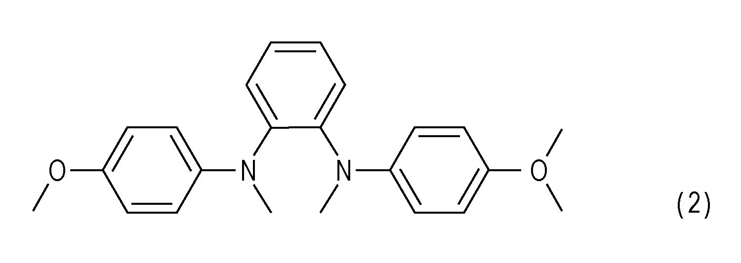
被酸化物質1は、以下の方法で合成した。まず、反応容器に、酢酸パラジウムを150mgと、トリtert-ブチルリンの0.2g/mLトルエン液を1.68mL加え、30分撹拌した。その後、1,2-ジブロモベンゼンを3.91g、N-メチル-p-アニシジンを5.0g、ナトリウムtert-ブトキサイドを4.79g、トルエンを5g加え、窒素雰囲下120℃で24時間反応させた。さらに、酢酸パラジウムを150mg、トリtert-ブチルリンのトルエン液を1.68mL加え、36時間反応した後、放冷した。得られた懸濁液を水、酢酸エチルに加えて洗浄し不要物を除去した後、水層を酢酸エチルで抽出、有機層をあわせて水、食塩水で洗浄を行い、乾燥、濃縮して粉末を得た。これをカラム精製、分取GPCで生成を行い、被酸化物質1を得た。
(実施例3)
[被酸化物質2の合成]
被酸化物質2として、以下の構造式(3)で表わされる化合物を合成した。
[被酸化物質2の合成]
被酸化物質2として、以下の構造式(3)で表わされる化合物を合成した。
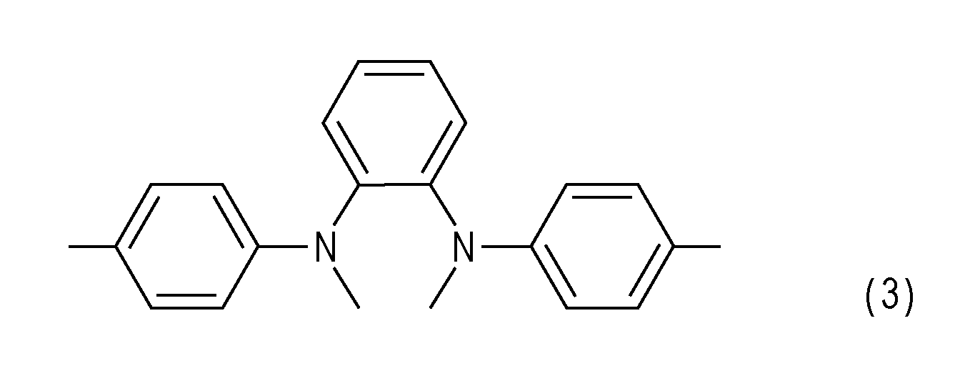
被酸化物質2は、実施例2における被酸化物質1の合成において、N-メチル-p-アニシジンを5.0g用いる代わりに、N-メチル-p-トルイジンを6.42g用いることにより、被酸化物質1の合成方法と同様の方法で合成した。
(実施例4)
[EC素子の作製]
第一の実施形態のEC素子100を、以下に説明する方法により作製する。
[EC素子の作製]
第一の実施形態のEC素子100を、以下に説明する方法により作製する。
第一の電極101、第二の電極102としてのインジウムドープ酸化スズ(ITO)膜が成膜されている基板104を二枚用意した。基板104は、透明導電性ガラスを用いる。次に、シール材105として、100μmのスペーサービーズを混合したUV硬化性の接着剤(TB3035B、スリーボンド社製)を、二枚の基板104それぞれの外周に塗布する。その後、ITO膜が対向するように二枚の基板104を重ね合わせて、UV光を照射することにより接着剤を硬化させ、二枚の基板104を接着してセルを作成する。作成したセルは、開口部110を有する。
アノード性EC化合物、カソード性EC化合物、及び被酸化物質1を溶媒に溶解させ、EC層103に含まれる電解質溶液とする。本実施例では、アノード性EC化合物として5,10-ジメチル-5,10-ジヒドロフェナジン(以下、「DMDHP」と呼ぶ)を用い、カソード性EC化合物としてヘプチルビオロゲントリフルオロメタンスルホン酸塩(以下「HV」と呼ぶ)を用いる。電解質溶液に含まれるDMDHP及びHVのそれぞれの濃度は50mM、被酸化物質1の濃度は5mMである。得られた電解質溶液を、開口部110から注入した後、上述のUV硬化性の接着剤を用いて封止材120で開口部110を封止することにより、EC素子100を得る。
本実施例では、取得部504として、光吸収量を測定する測定手段を有する。本実施例の検知手段は、光源150と、EC層103を通過した光源150からの光を検出する検出部151と、を有する。
具体的には、EC素子100の一対の基板104の一方の上面の一部に、基板104と接して2つの光源150を配置する。2つの照射手段は、一方が波長460nmの光を発光するLED、他方が波長595nmの光を発光するLEDである。2つの光源150のそれぞれが発光する光の波長は、EC層103に含まれるアノード性EC化合物及びカソード性EC化合物のそれぞれの着色体の吸収波長に対応する。そして、2つの光源150を配置した基板と対向する基板の下面に、2つの光源150のそれぞれからの光が入射するように検出部151を配置する。検出部151としては、フォトダイオードが用いられる。このように検知部151を設けることにより、EC化合物のそれぞれの着色体の吸収波長における吸光度を測定して、電荷バランスの情報として吸光度比を取得できる。
[酸化還元電位の測定]
本実施例で使用したEC化合物及び被酸化物質1について、酸化還元電位を測定して化合物の反応性を評価した。以下に、その具体的な方法及び結果を説明する。
本実施例で使用したEC化合物及び被酸化物質1について、酸化還元電位を測定して化合物の反応性を評価した。以下に、その具体的な方法及び結果を説明する。
0.1Mのテトラブチルアンモニウムヘキサフルオロフォスフェートの炭酸プロピレン(以下、「PC」と呼ぶ)溶液に、EC化合物としてのDMDHP、HV又は被酸化物質1をそれぞれ1mMで溶解させた溶液を調製した。次に、ITOを作用電極、白金を対抗電極、Ag/Ag+(PF6,PC)を参照電極として用いてCV測定を行った。
その結果、DMDHPの第一の酸化反応の半波電位は-0.62Vであり、不可逆的な酸化反応の電位は1.35Vである。また、HVの第一の還元反応の半波電位は-1.20Vであり、不可逆的な還元反応の電位は-2.60Vである。また、被酸化物質1が不可逆的に酸化される電位は、-0.18Vである。
このことから、被酸化物質1の酸化反応は、アノード性EC化合物の第一の酸化反応よりも起きにくく、アノード性EC材料の不可逆的な酸化反応よりも起こりやすいことが確認できた。すなわち、被酸化物質1は、条件(B)及び(C)、すなわち条件(i)を満たすことが確認できる。
[酸化時の吸収スペクトルの測定]
本実施例で使用したアノード性EC化合物であるDMDHPの第一の酸化体及び被酸化物質1の酸化体について、吸収スペクトルを測定した。
本実施例で使用したアノード性EC化合物であるDMDHPの第一の酸化体及び被酸化物質1の酸化体について、吸収スペクトルを測定した。
吸収スペクトルの測定は、以下の方法で行った。上述の酸化還元電位の測定と同様の溶液を調製し、各溶液に含まれるEC化合物又は被酸化物質1の酸化電位を印加した状態で、作用電極近傍の溶液の吸収スペクトルを測定した。なお、電圧を印加する際の電極は、作用電極として白金メッシュを、対抗電極として白金を、参照電極としてAg/Ag+(PF6,PC)を用いた。
図6は、測定した吸収スペクトルを示す図である。図6では、DMDHPの吸収スペクトルを実線で示し、被酸化物質1の吸収スペクトルを点線で示す。なお、本実施例のEC素子が対象とする波長領域は、425nm以上700nm以下の範囲とする。
本実施例において、被酸化物質1が不可逆的に酸化された場合の吸光度は、アノード性EC化合物が第一の酸化反応をされた場合の吸光度と比較して小さく、実質的に着色しないものとみなせる。
[EC素子の耐久駆動]
被酸化物質を用いた電荷リバランスを行わなかった場合のEC素子の耐久性の評価を行った。第一の電極101及び第二の電極102に0.8Vの電圧を印加して着色状態とし、着色状態のまま一週間経過させた後、第一の電極101と第二の電極102を短絡しEC素子100を消色駆動する。消色状態のEC素子100において、460nm及び595nmのそれぞれの吸光度を測定し、初期状態における吸光度からの吸光度の変化量を求めた。吸光度の変化量は、460nmで+0.10、595nmで±0.00であった。このことから、455nmに吸収ピークを持つアノード性EC化合物の着色体が残存して色残り(消色不良)が発生することが確認される。
被酸化物質を用いた電荷リバランスを行わなかった場合のEC素子の耐久性の評価を行った。第一の電極101及び第二の電極102に0.8Vの電圧を印加して着色状態とし、着色状態のまま一週間経過させた後、第一の電極101と第二の電極102を短絡しEC素子100を消色駆動する。消色状態のEC素子100において、460nm及び595nmのそれぞれの吸光度を測定し、初期状態における吸光度からの吸光度の変化量を求めた。吸光度の変化量は、460nmで+0.10、595nmで±0.00であった。このことから、455nmに吸収ピークを持つアノード性EC化合物の着色体が残存して色残り(消色不良)が発生することが確認される。
[消色不良の低減]
被酸化物質を用いて電荷リバランスを行うことにより色残りの低減を行う場合の、EC素子の駆動方法について説明する。本実施例では、取得部504としての測定手段の測定に基づいて、色残りが発生したら第一の電極101及び第二の電極102に印加する電圧を変更する。具体的には、以下のシーケンスを用いてEC装置500を駆動する。
被酸化物質を用いて電荷リバランスを行うことにより色残りの低減を行う場合の、EC素子の駆動方法について説明する。本実施例では、取得部504としての測定手段の測定に基づいて、色残りが発生したら第一の電極101及び第二の電極102に印加する電圧を変更する。具体的には、以下のシーケンスを用いてEC装置500を駆動する。
まず、測定手段の測定結果から、460nm又は595nmにおける吸光度の初期状態の吸光度からの変化量が、0.005より大きいと判断された場合、制御部503が駆動電源501の印加電圧を1.5Vに変更する。そして、1.5Vの電圧を印加時間10msで印加する。その後、460nmにおける吸光度の変化量が0.005より大きければ、再び1.5Vの電圧を10ms印加し、460nmにおける吸光度を測定する。460nmにおける吸光度の変化量が0.005以下、又は、595nmにおける吸光度の変化量が0.005以上となったら、電圧の印加を終了する。
その結果、本実施例のEC素子100は、駆動開始より約2分で460nmにおける変化量が0.005以下となり、電圧の印加を終了した。その結果、アノード性EC化合物の着色体が残存することによる色残りが、電荷リバランスを行う前の1/20以下に低減された。また、上述の駆動方法で電荷リバランスを行った直後のEC素子100は、EC層103において色残りが均一に低減され、ほとんど見えなくなることが目視により確認される。
一方、EC層に被酸化物質1を含まないEC素子で同様の操作を行っても、消色不良は残存する。
本実施例のEC素子によれば、電荷インバランスが発生することにより生じた、消色状態における色残りと、着色状態における吸収スペクトルの変化と、を低減できる。
(実施例5)
[EC素子の作製]
第二の実施形態のEC素子700を、以下に説明する方法により作製する。
[EC素子の作製]
第二の実施形態のEC素子700を、以下に説明する方法により作製する。
まず、フッ素ドープ酸化スズ(FTO)膜が成膜されている基板704を二枚用意する。基板704は、透明導電性ガラス(TEC15、日本板硝子製)を用いる。次に、ダイヤモンド工具を用いて、点線783の位置のFTO膜を除去する。これにより、FTO膜は、第一の電極701又は第二の電極702となる基板704の中央に配置されているFTO膜と、第一の電極701又は第二の電極702とは電気的に独立している第三の電極730の形成領域に配置されているFTO膜と、に分割される。
続いて、アンチモンドープ酸化スズナノ粒子(石原産業社製)12gと、濃硝酸2mLと、水200mLと、を混合し、80℃で8時間攪拌後、真空乾燥1日行うことで、酸化スズナノ粒子のケーキを得た。次に、このケーキ4gに、水20mL、ポリエチレングリコール1.2g及びヒドロキシプロピルセルロース0.4gを加えた後、15日間撹拌を行うことでスラリーを調製した。調整したスラリーを、第三の電極730の形成領域にあるFTO膜に塗布して500℃、30分の条件で焼成することにより、第三の電極730としてのアンチモンドープ酸化スズナノ粒子膜(以下、「ナノ粒子膜」ということがある。)を得た。このとき、形成したナノ粒子膜の比表面積は450cm2/cm2であった。
第三の電極730を形成した二枚の基板704に、100μmのスペーサービーズを混合したUV硬化性の接着剤(TB3035B、スリーボンド社製)を用いて、シール材705を接着した。その際、第一の電極701と第二の電極702とが対向し且つ第三の電極730同士が対向し、さらに電極取出部位780が露出するように、二枚の基板704を重ね合わせる。シール材705は、その一部に開口部710を有する。接着剤は、UV光を照射することで硬化する。
EC層703に含まれる電解質溶液を作製する。本実施例の電解質溶液は、カソード性EC化合物、アノード性の酸化還元物質及び被還元物質1を含む。電解質溶液は、カソード性EC化合物としてのHVと、アノード性の酸化還元物質としてのフェロセンと、被還元物質1と、を溶媒に溶解させて調製する。電解質溶液に含まれるフェロセン及びHVのそれぞれの濃度を50mM、被還元物質1の濃度を5mMとした。作製した電解質溶液を、開口部710から注入した後、上述のUV硬化性の接着剤を用いて封止材720で開口部710を封止することにより、EC素子700を得る。
本実施例では、取得部504として、光吸収を測定して電荷バランスを検知する測定手段を設ける。測定手段は、波長595nmの光を照射及び検出する構成とした以外は実施例4と同様である。
[酸化還元電位の測定]
本実施例で使用したEC化合物及び被還元物質1について、酸化還元電位を測定して各化合物の反応性を評価する。酸化還元電位を測定する方法は、実施例4と同様である。その結果、HVの第一の還元反応の半波電位は-1.20Vであり、不可逆的な還元反応の電位は-2.60Vである。また、被還元物質1が不可逆的に還元される電位は、-1.35Vである。
本実施例で使用したEC化合物及び被還元物質1について、酸化還元電位を測定して各化合物の反応性を評価する。酸化還元電位を測定する方法は、実施例4と同様である。その結果、HVの第一の還元反応の半波電位は-1.20Vであり、不可逆的な還元反応の電位は-2.60Vである。また、被還元物質1が不可逆的に還元される電位は、-1.35Vである。
この結果から、被還元物質1の不可逆的な還元反応は、カソード性EC化合物の第一の還元反応よりも起きにくく、カソード性EC材料の不可逆的な還元反応よりも起こりやすいことが確認できた。すなわち、被還元物質1は、条件(F)及び(G)、すなわち条件(ii)を満たすことが確認できる。
[還元時の吸収スペクトルの測定]
カソード性EC化合物であるHVの第一の還元体及び被還元物質1の還元体について、吸収スペクトルを測定する。吸収スペクトルの測定方法は、HV又は被還元物質1が溶解した溶液を用い、それぞれが還元される電位を印加した以外は、実施例4と同様の方法で行う。
カソード性EC化合物であるHVの第一の還元体及び被還元物質1の還元体について、吸収スペクトルを測定する。吸収スペクトルの測定方法は、HV又は被還元物質1が溶解した溶液を用い、それぞれが還元される電位を印加した以外は、実施例4と同様の方法で行う。
図8は、測定した吸収スペクトルを示す図である。図8では、HVの吸収スペクトルを実線で示し、被還元物質1の吸収スペクトルを点線で示す。なお、本実施例のEC素子が対象とする波長領域は、425nm以上700nm以下の範囲とする。
本実施例において、被還元物質1が不可逆的に酸化された場合の吸光度は、カソード性EC化合物が第一の還元反応をされた場合の吸光度と比較して小さく、実質的に着色しないものとみなせる。
[EC素子の耐久駆動]
被還元物質を用いた電荷リバランスを行わなかった場合の本実施例のEC素子700の耐久性の評価を行う。耐久性の評価の方法は、EC素子を着色状態とする際に第一の電極701及び第二の電極702に印加する電圧を1.0Vとした以外は、実施例4と同様である。消色状態のEC素子において、595nmの吸光度を測定し、初期状態における吸光度からの吸光度の変化量を求めたところ、吸光度の変化量は±0.10である。このことから、カソード性EC化合物の着色体が残存して色残り(消色不良)が発生していることが確認される。
被還元物質を用いた電荷リバランスを行わなかった場合の本実施例のEC素子700の耐久性の評価を行う。耐久性の評価の方法は、EC素子を着色状態とする際に第一の電極701及び第二の電極702に印加する電圧を1.0Vとした以外は、実施例4と同様である。消色状態のEC素子において、595nmの吸光度を測定し、初期状態における吸光度からの吸光度の変化量を求めたところ、吸光度の変化量は±0.10である。このことから、カソード性EC化合物の着色体が残存して色残り(消色不良)が発生していることが確認される。
[消色不良の低減]
被還元物質を用いて電荷リバランスを行うことにより色残りの低減を行う場合の、EC素子の駆動方法について説明する。本実施例では、検知手段の検知結果から色残りが発生していると判断された場合、色残りを低減するために、第一の電極701と第二の電極702と被還元物質1が還元される電圧を印加する。具体的には、以下のシーケンスを用いて駆動する。
被還元物質を用いて電荷リバランスを行うことにより色残りの低減を行う場合の、EC素子の駆動方法について説明する。本実施例では、検知手段の検知結果から色残りが発生していると判断された場合、色残りを低減するために、第一の電極701と第二の電極702と被還元物質1が還元される電圧を印加する。具体的には、以下のシーケンスを用いて駆動する。
まず、検知手段の検知結果から、595nmにおける吸光度の変化量が0.005より大きいと判断された場合、制御部503が駆動電源501の印加電圧を1.4Vに変更する。そして、1.4Vの電圧を印加時間10msで印加する。その後、595nmにおける吸光度の変化量が0.005より大きければ、再び1.4Vの電圧を10ms印加して、測定手段により吸光度を測定する。595nmにおける吸光度の変化量が0.005以下になった場合は、電圧の印加を終了する。
その結果、本実施例のEC素子によれば、駆動開始より約5分で595nmにおける吸光度の変化量が0.005以下となり、電圧の印加が終了した。カソード性EC化合物の着色体が残存することによる着色不良が、電荷リバランスを行う前の1/20以下に低減される。また、上述の駆動方法で電化リバランスを行った直後のEC素子700は、EC層703で消色不良が均一に低減されてほとんど見えなくなることが、目視により確認できる。
一方、EC層に被還元物質1を含まないEC素子は、同様の消色不良低減のための駆動を行っても、消色不良は残存する。
本実施例のEC素子によれば、電荷インバランスが発生することにより生じた、消色状態における色残りと、着色状態における吸収スペクトルの変化と、を低減できる。
(実施例6)
[EC素子の作製]
本実施例のEC素子は、実施例4と同様の構成である。ただし、本実施例のEC層103に含まれる電解質溶液は、アノード性EC化合物、カソード性EC化合物、被酸化物質2、及び被還元物質1を含む。本実施例では、アノード性EC化合物としてDMDHPを用い、カソード性EC化合物としてHVを用いる。電解質溶液に含まれるDMDHP及びHVのそれぞれの濃度は50mM、被酸化物質2及び被還元物質1のそれぞれの濃度は5mMとする。
[EC素子の作製]
本実施例のEC素子は、実施例4と同様の構成である。ただし、本実施例のEC層103に含まれる電解質溶液は、アノード性EC化合物、カソード性EC化合物、被酸化物質2、及び被還元物質1を含む。本実施例では、アノード性EC化合物としてDMDHPを用い、カソード性EC化合物としてHVを用いる。電解質溶液に含まれるDMDHP及びHVのそれぞれの濃度は50mM、被酸化物質2及び被還元物質1のそれぞれの濃度は5mMとする。
[酸化還元電位の測定]
本実施例で使用したEC化合物、被酸化物質及び被還元物質について、実施例4、5と同様の方法で酸化還元電位を測定して反応性を評価する。その結果、被酸化物質2が不可逆的に酸化される電位は-0.35V、被還元物質1が不可逆的に還元される電位は-1.35Vであった。なお、DMDHP及びHVの酸化還元電位は、上述の実施例と同じである。
本実施例で使用したEC化合物、被酸化物質及び被還元物質について、実施例4、5と同様の方法で酸化還元電位を測定して反応性を評価する。その結果、被酸化物質2が不可逆的に酸化される電位は-0.35V、被還元物質1が不可逆的に還元される電位は-1.35Vであった。なお、DMDHP及びHVの酸化還元電位は、上述の実施例と同じである。
このことから、被酸化物質2の酸化反応は、アノード性EC化合物の第一の酸化反応よりも起きにくく(酸化される電位が正であり)、アノード性EC材料の不可逆的な第二の酸化反応よりも起こりやすいことが確認できる。すなわち、被酸化物質2は、条件(B)及び(C)、すなわち条件(i)を満たす。また、被還元物質1の還元反応は、カソード性EC化合物の第一の還元反応よりも起きにくく、カソード性EC材料の不可逆的な第二の還元反応よりも起こりやすいことが確認できる。すなわち、被還元物質1は、条件(F)及び(G)、すなわち条件(ii)を満たす。
[酸化還元時の吸収スペクトルの測定]
被還元物質1の還元体及び被酸化物質2の酸化体のそれぞれについて、吸収スペクトルを測定する。吸収スペクトルの測定方法は、被還元物質1の還元体又は被酸化物質2を溶解した溶液を用いた以外は、実施例4、5と同様の方法で行う。
被還元物質1の還元体及び被酸化物質2の酸化体のそれぞれについて、吸収スペクトルを測定する。吸収スペクトルの測定方法は、被還元物質1の還元体又は被酸化物質2を溶解した溶液を用いた以外は、実施例4、5と同様の方法で行う。
その結果、本実施例のEC素子が対象とする波長領域である425nm以上700nm以下の範囲において、被還元物質1の還元体の吸光度は、カソード性EC化合物が第一の還元反応をされた場合の吸光度と比較して小さい。また、本実施例のEC素子が対象とする波長領域である425nm以上700nm以下の範囲において、被酸化物質2の酸化体の吸光度は、アノード性EC化合物が第一の酸化反応をされた場合の吸光度と比較して小さい。以上のことから、被酸化物質2及び被還元物質1のそれぞれは、不可逆的に酸化又は還元されても、実質的に着色しないものとみなせる。
[EC素子の耐久駆動]
実施例4、5と同様の方法で、被酸化物質及び被還元物質を用いた電荷リバランスを行わなかった場合の本実施例のEC素子の耐久性の評価を行う。その結果、着色状態で一週間経過した後のEC素子では、460nmにおける吸光度の変化量は+0.10、595nmにおける吸光度の変化量は±0.00であった。このことから、アノード性EC化合物の着色体が残存して色残り(消色不良)が発生していることが確認できる。
実施例4、5と同様の方法で、被酸化物質及び被還元物質を用いた電荷リバランスを行わなかった場合の本実施例のEC素子の耐久性の評価を行う。その結果、着色状態で一週間経過した後のEC素子では、460nmにおける吸光度の変化量は+0.10、595nmにおける吸光度の変化量は±0.00であった。このことから、アノード性EC化合物の着色体が残存して色残り(消色不良)が発生していることが確認できる。
[消色不良の低減]
本実施例では、実施例4と同様のシーケンスを用いて、被酸化物質及び被還元物質を用いて電荷リバランスを行うことにより消色不良の低減を行う。
本実施例では、実施例4と同様のシーケンスを用いて、被酸化物質及び被還元物質を用いて電荷リバランスを行うことにより消色不良の低減を行う。
その結果、駆動開始より約2分で460nmにおける変化量が0.005以下となり、電圧の印加を終了した。電圧の印加を終了した後のEC素子では、アノード性EC化合物の着色体が残存することによる色残りが、電荷リバランスを行う前の1/20以下に低減された。また、上述の駆動方法で電荷リバランスを行った直後のEC素子は、EC層において色残りが均一に低減され、ほとんど見えなくなることが目視により確認できる。
本実施例のEC素子によれば、電荷インバランスが発生することにより生じた、消色状態における色残りと、着色状態における吸収スペクトルの変化と、を低減できる。
以上、本発明の好ましい実施形態について説明したが、本発明はこれらの実施形態に限定されず、その要旨の範囲内で種々の変形及び変更が可能である。
例えば、上述の実施形態では、取得部504として吸光量や電位を測定する測定手段を用いて電荷バランスの情報と取得しているが、このような構成に限定するものではなく、取得部504を有していなくてもよい。
(実施例7)
実施例4と同様の方法でEC素子の作製、酸化還元電位の測定、酸化時の吸収スペクトルの測定、EC素子の耐久駆動を行う。
実施例4と同様の方法でEC素子の作製、酸化還元電位の測定、酸化時の吸収スペクトルの測定、EC素子の耐久駆動を行う。
[消色不良の低減]
被酸化物質を用いて電荷リバランスを行うことにより色残りの低減を行う場合の、EC素子の駆動方法について説明する。本実施例では、取得部504としての測定手段の測定に基づいて、色残りが発生したら第一の電極101及び第二の電極102に流れる電流を制御する。具体的には、以下のシーケンスを用いてEC装置500を駆動する。
被酸化物質を用いて電荷リバランスを行うことにより色残りの低減を行う場合の、EC素子の駆動方法について説明する。本実施例では、取得部504としての測定手段の測定に基づいて、色残りが発生したら第一の電極101及び第二の電極102に流れる電流を制御する。具体的には、以下のシーケンスを用いてEC装置500を駆動する。
まず、測定手段の測定結果から、460nm又は595nmにおける吸光度の初期状態の吸光度からの変化量が、0.005より大きいと判断された場合、まず、EC素子の駆動を通常のフル着色状態とする。その上で、制御部503が駆動電流を通常のフル着色時の1.1倍に変更して10ms印加する。その後、消色して460nmにおける吸光度の変化量が0.005より大きければ、再び同様の方法で、通常のフル着色時の1.1倍の電流を10ms印加し、再び消色して460nmにおける吸光度を測定する。460nmにおける吸光度の変化量が0.005以下、又は、595nmにおける吸光度の変化量が0.005以上となったら、電流制御を終了する。
その結果、本実施例のEC素子100は、460nmにおける変化量が0.005以下となり、アノード性EC化合物の着色体が残存することによる色残りが、電荷リバランスを行う前の1/20以下に低減された。また、上述の駆動方法で電荷リバランスを行った直後のEC素子100は、EC層103において色残りが均一に低減され、ほとんど見えなくなることが目視により確認される。
一方、EC層に被酸化物質1を含まないEC素子で同様の操作を行っても、消色不良は残存する。
本実施例のEC装置によれば、電荷インバランスが発生することにより生じた、消色状態における色残りと、着色状態における吸収スペクトルの変化と、を低減できる。
本発明は上記実施の形態に制限されるものではなく、本発明の精神及び範囲から離脱することなく、様々な変更及び変形が可能である。従って、本発明の範囲を公にするために以下の請求項を添付する。
本願は、2016年07月23日提出の日本国特許出願特願2016-144986を基礎として優先権を主張するものであり、その記載内容の全てをここに援用する。
Claims (20)
- 第一の電極と、第二の電極と、前記第一の電極と前記第二の電極との間に配置されているエレクトロクロミック層と、を有するエレクトロクロミック素子と、前記エレクトロクロミック素子の制御部と、を有するエレクトロクロミック装置であって、
前記エレクトロクロミック層は、アノード性エレクトロクロミック化合物、及び、被酸化物質と、を有し、
前記被酸化物質は、酸化による色変化を実質的に生じない、かつ前記被酸化物質の酸化体は還元されない、物質であり、
前記被酸化物質の酸化反応は、前記アノード性エレクトロクロミック化合物の可逆的な酸化反応よりも起こりにくく、かつ前記アノード性エレクトロクロミック化合物の不可逆的な酸化反応よりも起こりやすく、
前記制御部は、エレクトロクロミック素子の電荷のバランスに基づいて前記被酸化物質を酸化する制御を行うエレクトロクロミック装置。 - 前記エレクトロクロミック層は、カソード性エレクトロクロミック化合物、及び、被還元物質をさらに有し、
前記被還元物質は、還元による色変化を実質的に生じない、かつ前記被還元物質の還元体は酸化されない、物質であり、
前記被還元物質の還元反応は、前記カソード性エレクトロクロミック化合物の可逆的な還元反応よりも起こりにくく、かつ前記カソード性エレクトロクロミック化合物の不可逆な還元反応よりも起こりやすいクレーム1に記載のエレクトロクロミック装置。 - 前記エレクトロクロミック層は、可逆的に酸化される酸化還元物質を更に有し、
前記酸化還元物質の酸化反応は、前記アノード性エレクトロクロミック化合物の可逆的な酸化反応よりも起こりやすく、前記アノード性エレクトロクロミック化合物の不可逆的な酸化反応よりも起こりにくいクレーム1に記載のエレクトロクロミック装置。 - 第一の電極と、第二の電極と、前記第一の電極と前記第二の電極との間に配置されているエレクトロクロミック層と、を有するエレクトロクロミック素子と、前記エレクトロクロミック素子の制御部と、を有するエレクトロクロミック装置であって、
前記エレクトロクロミック層は、カソード性エレクトロクロミック化合物、及び、被還元物質と、を有し、
前記被還元物質は、還元による色変化を実質的に生じない、かつ前記被還元物質の還元体は酸化されない、物質であり、
前記被還元物質の還元反応は、前記カソード性エレクトロクロミック化合物の可逆的な還元反応よりも起こりにくく、かつ前記カソード性エレクトロクロミック化合物の不可逆的な還元反応よりも起こりやすく、
前記制御部は、エレクトロクロミック素子の電荷のバランスに基づいて前記被還元物質を還元する制御を行うエレクトロクロミック装置。 - 前記エレクトロクロミック層は、可逆的に還元される酸化還元物質を更に有し、
前記酸化還元物質の可逆的な還元反応は、前記カソード性エレクトロクロミック化合物の可逆的な還元反応よりも起こりやすく、前記カソード性エレクトロクロミック化合物の不可逆的な還元反応よりも起こりにくい請求項4に記載のエレクトロクロミック装置。 - 前記第一の電極及び前記第二の電極のそれぞれと異なる位置に配置されている第三の電極を有する請求項1に記載のエレクトロクロミック装置。
- 前記エレクトロクロミック素子の電荷バランスの情報を取得する取得部を有し、
前記制御部は、前記取得部の前記情報に基づいて前記エレクトロクロミック素子に印加する電圧を変更する請求項1に記載のエレクトロクロミック装置。 - 前記エレクトロクロミック素子の電荷バランスの情報を取得する取得部を有し、
前記制御部は、前記取得部の前記情報に基づいて前記エレクトロクロミック素子に印加する電圧を変更する請求項4に記載のエレクトロクロミック装置。 - 前記取得部は、前記エレクトロクロミック層の光吸収量を測定する測定手段である請求項7に記載のエレクトロクロミック装置。
- 前記取得部は、前記エレクトロクロミック層の光吸収量を測定する測定手段である請求項8に記載のエレクトロクロミック装置。
- 前記制御部は、前記電荷バランスの情報から電荷インバランスが発生していると判断した場合は、前記エレクトロクロミック素子に印加する電圧を変更することにより、第一の電位から第二の電位に変更する請求項7に記載のエレクトロクロミック装置。
- 前記第一の電位は、前記アノード性エレクトロクロミック化合物が可逆的に酸化され且つ前記被酸化物質が不可逆的に酸化されない電位、又は前記カソード性エレクトロクロミック化合物が可逆的に還元され且つ前記被還元物質が不可逆的に還元されない電位である請求項11に記載のエレクトロクロミック装置。
- 前記第二の電位は、前記被酸化物質の不可逆的な酸化反応が起こり、かつ前記アノード性エレクトロクロミック化合物の不可逆的な酸化反応が起こらない電位、又は、前記被還元物質の不可逆的な還元反応が起こり、かつ前記カソード性エレクトロクロミック化合物の不可逆的な還元反応が起こらない電位である請求項11に記載のエレクトロクロミック装置。
- 請求項1に記載のエレクトロクロミック装置と、
前記エレクトロクロミック素子に接続されており、前記エレクトロクロミック素子を駆動する能動素子と、を有する光学フィルタ。 - 請求項4に記載のエレクトロクロミック装置と、
前記エレクトロクロミック素子に接続されており、前記エレクトロクロミック素子を駆動する能動素子と、を有する光学フィルタ。 - 請求項14に記載の光学フィルタと、
複数のレンズを有する撮像光学系と、を有するレンズユニット。 - 複数のレンズを有する撮像光学系と、
請求項14に記載の光学フィルタと、
前記光学フィルタを透過した光を受光する受光素子と、を有する撮像装置。 - 一対の基板と、
前記一対の基板の間に配置されている請求項1に記載のエレクトロクロミック装置と、
前記エレクトロクロミック装置に接続され、前記エレクトロクロミック装置により前記一対の基板を透過する光の光量を調整する能動素子と、を有する窓材。 - 一対の電極と、前記一対の電極の間に配置されているエレクトロクロミック層とを有するエレクトロクロミック素子の駆動方法であって、
前記一対の電極間の電荷のバランスを検知する検知ステップと、
前記検知ステップにおける検知結果に基づいて前記エレクトロクロミック素子に電圧または電流を印加する印加ステップと、を有することを特徴とする駆動方法。 - 前記印加ステップにおける前記電圧または前記電流は、エレクトロクロミック素子を着色させる場合に印加される電圧または電流よりも大きい請求項19に記載の駆動方法。
Priority Applications (1)
| Application Number | Priority Date | Filing Date | Title |
|---|---|---|---|
| US16/253,912 US11180950B2 (en) | 2016-07-23 | 2019-01-22 | Electrochromic device, optical filter, lens unit, imaging apparatus, window member, and driving method |
Applications Claiming Priority (2)
| Application Number | Priority Date | Filing Date | Title |
|---|---|---|---|
| JP2016-144986 | 2016-07-23 | ||
| JP2016144986 | 2016-07-23 |
Related Child Applications (1)
| Application Number | Title | Priority Date | Filing Date |
|---|---|---|---|
| US16/253,912 Continuation US11180950B2 (en) | 2016-07-23 | 2019-01-22 | Electrochromic device, optical filter, lens unit, imaging apparatus, window member, and driving method |
Publications (1)
| Publication Number | Publication Date |
|---|---|
| WO2018021168A1 true WO2018021168A1 (ja) | 2018-02-01 |
Family
ID=61016511
Family Applications (1)
| Application Number | Title | Priority Date | Filing Date |
|---|---|---|---|
| PCT/JP2017/026393 Ceased WO2018021168A1 (ja) | 2016-07-23 | 2017-07-21 | エレクトロクロミック装置、光学フィルタ、レンズユニット、撮像装置、窓材、及び駆動方法 |
Country Status (3)
| Country | Link |
|---|---|
| US (1) | US11180950B2 (ja) |
| JP (1) | JP6991738B2 (ja) |
| WO (1) | WO2018021168A1 (ja) |
Cited By (2)
| Publication number | Priority date | Publication date | Assignee | Title |
|---|---|---|---|---|
| JP2020154072A (ja) * | 2019-03-19 | 2020-09-24 | 株式会社リコー | エレクトロクロミック装置、並びに、それを有するデバイス、窓、プロジェクションスクリーン、加飾材及び服飾材 |
| CN117288825A (zh) * | 2023-11-22 | 2023-12-26 | 山西阳光三极科技股份有限公司 | 煤矿设备安全管控方法及系统 |
Families Citing this family (7)
| Publication number | Priority date | Publication date | Assignee | Title |
|---|---|---|---|---|
| JP7486578B2 (ja) * | 2019-10-18 | 2024-05-17 | ビトロ フラット グラス エルエルシー | エレクトロクロミックデバイス、並びにその製造方法および操作方法 |
| US11709407B2 (en) | 2020-02-14 | 2023-07-25 | Gentex Corporation | Immobilized buffers in electroactive devices |
| US11966139B2 (en) | 2020-07-31 | 2024-04-23 | Ricoh Company, Ltd. | Electrochromic element, and method for driving the same |
| JP7687074B2 (ja) * | 2020-07-31 | 2025-06-03 | 株式会社リコー | エレクトロクロミック素子、及びその駆動方法 |
| JP7770847B2 (ja) * | 2020-11-26 | 2025-11-17 | キヤノン株式会社 | 撮像機器 |
| CN114995001B (zh) * | 2021-03-01 | 2023-10-13 | 中国科学院上海硅酸盐研究所 | 一种电致发射率可变器件 |
| CN118647926A (zh) * | 2022-02-18 | 2024-09-13 | 金泰克斯公司 | 多层低电流电光组合件 |
Citations (6)
| Publication number | Priority date | Publication date | Assignee | Title |
|---|---|---|---|---|
| JPH02287515A (ja) * | 1989-04-28 | 1990-11-27 | Toyota Central Res & Dev Lab Inc | エレクトロクロミック素子用電解質 |
| JPH0472272U (ja) * | 1990-10-31 | 1992-06-25 | ||
| JP2007286570A (ja) * | 2006-02-09 | 2007-11-01 | Casio Comput Co Ltd | エレクトロクロミック表示装置及び表示駆動装置 |
| JP2015166338A (ja) * | 2014-02-12 | 2015-09-24 | キヤノン株式会社 | 有機化合物及びこれを用いたエレクトロクロミック素子 |
| JP2016095503A (ja) * | 2014-11-06 | 2016-05-26 | キヤノン株式会社 | 有機エレクトロクロミック素子、光学フィルタ、レンズユニット、撮像装置 |
| JP2017146590A (ja) * | 2016-02-17 | 2017-08-24 | キヤノン株式会社 | エレクトロクロミック素子、およびその駆動方法、光学フィルタ、レンズユニット及び撮像装置 |
Family Cites Families (5)
| Publication number | Priority date | Publication date | Assignee | Title |
|---|---|---|---|---|
| JPH0359545A (ja) * | 1989-07-28 | 1991-03-14 | Nissan Motor Co Ltd | エレクトロクロミック素子 |
| US6188505B1 (en) | 1999-08-19 | 2001-02-13 | Gentex Corporation | Color-stabilized electrochromic devices |
| JP4816069B2 (ja) | 2005-12-26 | 2011-11-16 | ソニー株式会社 | エレクトロクロミック装置 |
| US8928966B1 (en) | 2012-08-08 | 2015-01-06 | Gentex Corporation | Electrochromic polyelectrolyte gel medium having improved creep resistance and associated electrochromic device |
| JP6429575B2 (ja) | 2013-12-03 | 2018-11-28 | キヤノン株式会社 | 新規有機化合物およびそれを有するエレクトロクロミック素子 |
-
2017
- 2017-05-12 JP JP2017095950A patent/JP6991738B2/ja active Active
- 2017-07-21 WO PCT/JP2017/026393 patent/WO2018021168A1/ja not_active Ceased
-
2019
- 2019-01-22 US US16/253,912 patent/US11180950B2/en active Active
Patent Citations (6)
| Publication number | Priority date | Publication date | Assignee | Title |
|---|---|---|---|---|
| JPH02287515A (ja) * | 1989-04-28 | 1990-11-27 | Toyota Central Res & Dev Lab Inc | エレクトロクロミック素子用電解質 |
| JPH0472272U (ja) * | 1990-10-31 | 1992-06-25 | ||
| JP2007286570A (ja) * | 2006-02-09 | 2007-11-01 | Casio Comput Co Ltd | エレクトロクロミック表示装置及び表示駆動装置 |
| JP2015166338A (ja) * | 2014-02-12 | 2015-09-24 | キヤノン株式会社 | 有機化合物及びこれを用いたエレクトロクロミック素子 |
| JP2016095503A (ja) * | 2014-11-06 | 2016-05-26 | キヤノン株式会社 | 有機エレクトロクロミック素子、光学フィルタ、レンズユニット、撮像装置 |
| JP2017146590A (ja) * | 2016-02-17 | 2017-08-24 | キヤノン株式会社 | エレクトロクロミック素子、およびその駆動方法、光学フィルタ、レンズユニット及び撮像装置 |
Cited By (3)
| Publication number | Priority date | Publication date | Assignee | Title |
|---|---|---|---|---|
| JP2020154072A (ja) * | 2019-03-19 | 2020-09-24 | 株式会社リコー | エレクトロクロミック装置、並びに、それを有するデバイス、窓、プロジェクションスクリーン、加飾材及び服飾材 |
| CN117288825A (zh) * | 2023-11-22 | 2023-12-26 | 山西阳光三极科技股份有限公司 | 煤矿设备安全管控方法及系统 |
| CN117288825B (zh) * | 2023-11-22 | 2024-02-06 | 山西阳光三极科技股份有限公司 | 煤矿设备安全管控方法及系统 |
Also Published As
| Publication number | Publication date |
|---|---|
| US20190171077A1 (en) | 2019-06-06 |
| US11180950B2 (en) | 2021-11-23 |
| JP2018022131A (ja) | 2018-02-08 |
| JP6991738B2 (ja) | 2022-01-13 |
Similar Documents
| Publication | Publication Date | Title |
|---|---|---|
| JP6991738B2 (ja) | エレクトロクロミック装置、光学フィルタ、レンズユニット、撮像装置、窓材、及び駆動方法 | |
| JP6812135B2 (ja) | エレクトロクロミック素子 | |
| US9869919B2 (en) | Electrochromic element, optical filter, lens unit, image pickup apparatus, and window member | |
| US10303033B2 (en) | Electrochromic element, optical filter, lens unit, and image pick-up apparatus | |
| US9766527B2 (en) | Electrochromic element, optical filter, lens unit, image pickup apparatus, and window member | |
| US10353263B2 (en) | Electrochromic element, method of driving the same, optical filter, lens unit, image pick-up apparatus, and window | |
| JP6758814B2 (ja) | 有機エレクトロクロミック素子、光学フィルタ、レンズユニット、撮像装置 | |
| US20060203322A1 (en) | Gel polymers containing ionic liquids | |
| KR101109253B1 (ko) | 플렉서블 전기변색 소자 및 그 제조방법 | |
| JP6957155B2 (ja) | エレクトロクロミック素子、およびその駆動方法、光学フィルタ、レンズユニット及び撮像装置 | |
| JP2014159385A (ja) | エレクトロクロミック化合物、エレクトロクロミック組成物、表示素子 | |
| JP6896400B2 (ja) | エレクトロクロミック装置、それを用いた光学フィルタ、レンズユニット、撮像装置、窓材及びエレクトロクロミック素子の駆動方法 | |
| JP6808363B2 (ja) | エレクトロクロミック素子及びその駆動方法、並びに光学フィルタ、レンズユニット、撮像装置及び窓材 | |
| JP6213080B2 (ja) | エレクトロクロミック材料、エレクトロクロミック組成物及びエレクトロクロミック表示素子 | |
| CN111183392B (zh) | 电致变色元件、滤光器、透镜单元、图像拾取装置和窗构件 | |
| JP2010175877A (ja) | 表示素子、それを用いた光学シャッター及び表示素子装置 | |
| JP7289692B2 (ja) | エレクトロクロミック素子及びこれを用いた撮像装置、透過率可変窓 | |
| JP6752632B2 (ja) | エレクトロクロミック素子、光学フィルタ、レンズユニット、撮像装置及び窓材 | |
| US12078904B2 (en) | Electrochromic device, optical filter, lens unit, image pickup apparatus, window member, and electrochromic mirror | |
| JP6758916B2 (ja) | エレクトロクロミック素子及びその駆動方法、並びに光学フィルタ、レンズユニット、撮像装置及び窓材 | |
| JP7786815B2 (ja) | エレクトロクロミック素子、及びそれを有する光学フィルタ、レンズユニット、撮像装置、窓材、エレクトロクロミックミラー | |
| JP5939034B2 (ja) | エレクトロクロミック化合物、エレクトロクロミック組成物、及び表示素子 | |
| JP5962208B2 (ja) | エレクトロクロミック化合物、エレクトロクロミック組成物、及び表示素子 | |
| JP2011017873A (ja) | エレクトロクロミック表示装置及びその駆動方法 | |
| JP6387673B2 (ja) | エレクトロクロミック化合物、エレクトロクロミック組成物及び表示素子及び調光素子 |
Legal Events
| Date | Code | Title | Description |
|---|---|---|---|
| 121 | Ep: the epo has been informed by wipo that ep was designated in this application |
Ref document number: 17834176 Country of ref document: EP Kind code of ref document: A1 |
|
| NENP | Non-entry into the national phase |
Ref country code: DE |
|
| 122 | Ep: pct application non-entry in european phase |
Ref document number: 17834176 Country of ref document: EP Kind code of ref document: A1 |